hyve: hybrid vertex-edge memory hierarchy for energy-efficient … · 2019-01-18 · the detailed...
TRANSCRIPT

0018-9340 (c) 2018 IEEE. Personal use is permitted, but republication/redistribution requires IEEE permission. See http://www.ieee.org/publications_standards/publications/rights/index.html for more information.
This article has been accepted for publication in a future issue of this journal, but has not been fully edited. Content may change prior to final publication. Citation information: DOI 10.1109/TC.2019.2893384, IEEETransactions on Computers
IEEE TRANSACTIONS ON COMPUTER, SPECIAL SECTION ON EMERGING NON-VOLATILE MEMORY TECHNOLOGIES 1
HyVE: Hybrid Vertex-Edge Memory Hierarchyfor Energy-Efficient Graph Processing
Guohao Dai,Tianhao Huang,Yu Wang, Senior Member, IEEE,Huazhong Yang, Senior Member, IEEE, and John Wawrzynek, Member, IEEE
Abstract—High energy consumption of conventional memory modules (e.g., DRAMs) hinders the further improvement of large-scalegraph processing’s energy efficiency. The emerging resistive random-access memory (ReRAM) has shown great potential in providingan energy-efficient memory module. However, the performance of ReRAMs suffers from data access patterns with poor locality andlarge amounts of written data, which are common in graph processing. In this paper, we propose HyVE, a Hybrid Vertex-Edge memoryhierarchy for energy-efficient graph processing. In HyVE, we avoid random access and data written to ReRAM modules. HyVE canreduce memory energy consumption by 86.17% compared with conventional memory systems. We have also proposed data sharingand bank-level power-gating schemes, which improve the energy efficiency by 1.60x and 1.53x. By analyzing the graph processingmodel on ReRAMs, we show that ReRAMs are good for read-intensive operations in graph processing (e.g., reading edges), whileReRAM crossbars are not suitable for processing edges because of heavy writing overheads. Our evaluations show that the optimizeddesign achieves two orders of magnitude and 5.90x energy efficiency improvement compared with the CPU-based and conventionalmemory hierarchy based designs, respectively. Moreover, HyVE achieves 2.83x energy reduction compared with the previousReRAM-based graph processing architecture.
Index Terms—resistive random-access memory (ReRAM), large-scale graph processing, energy efficiency, power-gating.
F
1 INTRODUCTION
G RAPHS have been widely used to represent relation-ships among real-world entities in various domains,
such as social networks and webpage hyperlinks. Ever-growing demands for large-scale graph data processing indata centers and mobile devices pose challenges to bothspeed and energy efficiency. Compared with graph pro-cessing frameworks developed on clusters [1–6] or a singlePC [7–12], accelerators [13–21] concentrate more on theenergy efficiency. Most graph processing applications arememory-bound. Therefore, with well-designed schedulingof data access, graph processing accelerators show enor-mous potential in energy efficiency without performancecompromises (e.g., Graphicionado [14] achieves 50x energyefficiency compared with CPU implementations).
However, the energy efficiency of accelerators is nega-tively influenced by modern high-performance but energy-hungry memory modules. Power breakdown results [22]show that over 60% of energy is consumed by memory forPageRank. In Graphicionado [14], the energy consumptionof memory is even higher (90%). Memory energy usage,which has been a problem in CPU-based platforms, poses
• Guohao Dai1, Yu Wang2, and Huazhong Yang are with the Dept. of E.E.,Beijing National Research Center for Information Science and Technology(BNRist), Beijing Innovation Center for Future Chip (ICFC), TsinghuaUniversity, Beijing, China, 100084.E-mail: [email protected], [email protected].
• Tianhao Huang was with the Dept. of E.E., Tsinghua University. Heis now with the Computer Science & Artificial Intelligence Laboratory,Massachusetts Institute of Technology, 32 Vassar Street, Cambridge,MA,United States, 02139.
• Prof. John Wawrzynek is with the Dept. of E.E.&C.S., University ofCalifornia, Berkeley, CA, United States, 94720.
Manuscript received by March 4th, 2018; revised by September 12th andDecember 26th, 2018; accepted by December 30th, 2018.
a more serious bottleneck in graph processing accelerators.High energy usage of main memory modules (e.g.,
DRAMs) is closely associated with the type and organi-zation of memory cells. The recent advancement in mem-ory technology offers possible solutions to some of thesechallenges. One of the most promising solutions is resistiverandom-access memory (ReRAM) [23, 24]. The ReRAM is anonvolatile memory (NVM) with much lower static energy,similar read delay but much higher write delay comparedwith DRAMs. Using ReRAMs alone is not sufficient foran energy-saving graph processing system without perfor-mance degradation due to the data access patterns of poorlocality and an enormous amount of write traffic. Thus,proper memory hierarchy design and data scheduling arekey to exploiting advantages of ReRAMs in graph process-ing accelerators.
In this paper, we propose a Hybrid Vertex-Edge memoryhierarchy, HyVE, for efficient graph processing. In HyVE,different types of graph data are stored in either ReRAMor conventional memories according to access patterns. Amemory controller is responsible for handling various re-quests from high-level accelerator logic. Techniques suchas vertices replacement scheduling and bank-level power-gating are introduced to HyVE to further improve theenergy efficiency. The contributions of this paper include:
• Hybrid memory hierarchy for graph data storage.We propose a hybrid memory hierarchy, HyVE, com-posed of both emerging ReRAMs and conventionalmemories (e.g., DRAMs and SRAMs) to achievehigher energy efficiency in graph processing. Verticesand edges in the graph are stored into different mem-ories according to their distinct data access patterns.

0018-9340 (c) 2018 IEEE. Personal use is permitted, but republication/redistribution requires IEEE permission. See http://www.ieee.org/publications_standards/publications/rights/index.html for more information.
This article has been accepted for publication in a future issue of this journal, but has not been fully edited. Content may change prior to final publication. Citation information: DOI 10.1109/TC.2019.2893384, IEEETransactions on Computers
IEEE TRANSACTIONS ON COMPUTER, SPECIAL SECTION ON EMERGING NON-VOLATILE MEMORY TECHNOLOGIES 2
1→0 0→7
2→3 2→43→4 3→7
4→1 4→5
6→2 6→07→1
B0, 0
B1, 0
B2, 0
B3, 0
B0, 1
B1, 1
B2, 1
B3, 1
B0, 2
B1, 2
B2, 2
B3, 2
B0, 3
B1, 3
B2, 3
B3, 3
0, 1
2, 3
4, 5
6, 7
I0
I1
I2
I3
0
1
4
3
2
5
6
7 0, 1
I0
2, 3
I1
4, 5
I2
6, 7
I3
sou
rce
inte
rva
ls
destination intervals
blo
cks
Fig. 1. Example graph (left) and interval-block partitioning (right).
Accesses to these data are well-scheduled to fullytake advantages of different types of memories.
• Data sharing among processing units. According toour HyVE design, vertices are transferred betweenthe on-chip memory of accelerators and off-chipmemory. We propose a data sharing scheme betweenon-chip and off-chip memories. In this way, weminimize data transferred and improve the energyefficiency of HyVE by 1.60x.
• Efficient power-gating scheme. Based on HyVE,we propose an aggressive power-gating scheme forgraph processing on ReRAMs to reduce backgroundenergy. It is made feasible by the nonvolatility ofReRAMs and nature of the edge-centric graph pro-cessing model. Such a design leads to 1.53x energyefficiency improvement.
• Working flow support for dynamic graphs. Graphsevolve in a real-world problem, and we propose awhole working flow of HyVE to support dynamicchanges in graphs. With the low overhead and in-ductive preprocessing scheme, HyVE can supportdynamic changes in graphs at the throughput of42.43 million edges per second per thread.
• Modeling of graph processing on ReRAMs. Weconduct a comprehensive analysis of graph process-ing on ReRAMs. By modeling both computation andmemory in graph processing, we compare the energyefficiency of HyVE with other ReRAM-based graphprocessing architecture. We show that ReRAMs aregood for read-intensive operations (e.g., readingedges), while suffering from heavy overheads ofconfiguring the adjacent matrix for processing edgesin graph processing. Experimental results also haveshown that HyVE can achieve 2.83x energy reductioncompared with the previous ReRAM-based graphprocessing architecture [19].
We have conducted extensive experiments to evaluatethe performance of HyVE and other graph processing ar-chitectures. Critical trade-off decisions are made in termsof ReRAM cell bit length and SRAM capacity. Our designfinally achieves at least 5.90x better energy efficiency com-pared with conventional memory systems on average. Theremainder of this paper is organized as follows:
Section 2 introduces the basis of graph processing mod-els and the ReRAM technology. The detailed architecture de-sign of HyVE is introduced in Section 3. We propose severalapproaches to improve the energy efficiency in Section 4.
Algorithm 1 Pseudo-code of the edge-centric model afterthe interval-block partitioningInput: G = (V,E), initializationOutput: Updated V
1: for each vi ∈ V do2: Initialize(vi, initialization)3: end for4: while not finished do5: for each Bx.y do6: for each ei.j ∈ Bx.y do7: value(vi) = Update(vi, vj)8: end for9: end for
10: end while11: return V
We also describe the dynamic graphs processing supportin Section 5. Then, we model the design of both HyVEand previous ReRAM-based graph processing architecturesin Section 6. Extensive experimental results are shown inSection 7, and Section 8 concludes the paper.
2 BACKGROUND AND MOTIVATION
2.1 Graph Processing ModelsGraph algorithms can be divided into graph computationand graph mining [25]. Graph computation algorithms,which calculate the value of each vertex in a graph, rangefrom Breadth-First Search (BFS) to PageRank. These algo-rithms can be described with the general Gather-Apply-Scatter (GAS) model. In GAS, different computations areperformed in the apply phase, depending on the imple-mented graph algorithms. In a shared-memory machine, wehave two simplified methods to implement GAS:
• Vertex-centric: Iterating over active vertices. All out-going neighbors’ properties are updated using thelocal property.
• Edge-centric: Iterating over edges. For each edge, thedestination is updated using the source’s property.
The edge-centric model was first proposed in X-Stream [9], emphasizing that the edge-centric algorithm hasbetter spatial locality. The edge-centric algorithm achievessequential access over edges at the cost of random ac-cesses over the vertices whose size is orders of magnitudesmaller than edges. Later, graph processing frameworkseither adopted the X-Stream-like algorithm or just sorted theedges to improve data locality. As a result, memory accesspatterns of graph processing consist of sequential reads overedges and random reads/writes over vertices. Such featuresline up well with the graph processing accelerator designbecause they involve lighter synchronization and communi-cation overheads, and many graph accelerators [18, 19, 26]have adopted this model.
Proper data partitioning also plays an important rolein the performance of graph processing. By adopting aninterval-block partitioning method, previous systems [11,12] only need to update one part of the graph at a time.Vertices are partitioned into P intervals according to in-dices, and edges are partitioned into P 2 blocks according
0018-9340 (c) 2018 IEEE. Personal use is permitted, but republication/redistribution requires IEEE permission. See http://www.ieee.org/publications_standards/publications/rights/index.html for more information.
This article has been accepted for publication in a future issue of this journal, but has not been fully edited. Content may change prior to final publication. Citation information: DOI 10.1109/TC.2019.2893384, IEEETransactions on Computers
IEEE TRANSACTIONS ON COMPUTER, SPECIAL SECTION ON EMERGING NON-VOLATILE MEMORY TECHNOLOGIES 3
wordline
bitline
gi,jDAC
DAC
DAC
ADC ADC ADCOxygen
Vacancies
TunnelingGap
V(t)
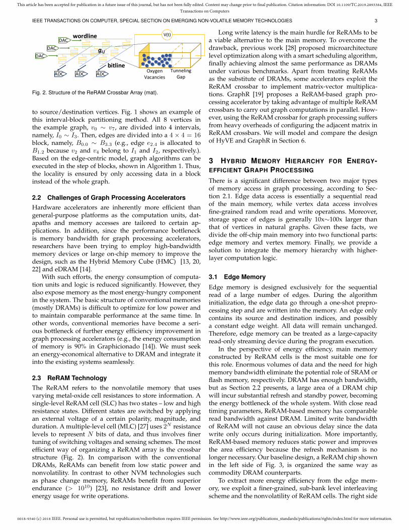
Fig. 2. Structure of the ReRAM Crossbar Array (mat).
to source/destination vertices. Fig. 1 shows an example ofthis interval-block partitioning method. All 8 vertices inthe example graph, v0 ∼ v7, are divided into 4 intervals,namely, I0 ∼ I3. Then, edges are divided into a 4 × 4 = 16block, namely, B0.0 ∼ B3.3 (e.g., edge e2.4 is allocated toB1.2 because v2 and v4 belong to I1 and I2, respectively.).Based on the edge-centric model, graph algorithms can beexecuted in the step of blocks, shown in Algorithm 1. Thus,the locality is ensured by only accessing data in a blockinstead of the whole graph.
2.2 Challenges of Graph Processing AcceleratorsHardware accelerators are inherently more efficient thangeneral-purpose platforms as the computation units, dat-apaths and memory accesses are tailored to certain ap-plications. In addition, since the performance bottleneckis memory bandwidth for graph processing accelerators,researchers have been trying to employ high-bandwidthmemory devices or large on-chip memory to improve thedesign, such as the Hybrid Memory Cube (HMC) [13, 20,22] and eDRAM [14].
With such efforts, the energy consumption of computa-tion units and logic is reduced significantly. However, theyalso expose memory as the most energy-hungry componentin the system. The basic structure of conventional memories(mostly DRAMs) is difficult to optimize for low power andto maintain comparable performance at the same time. Inother words, conventional memories have become a seri-ous bottleneck of further energy efficiency improvement ingraph processing accelerators (e.g., the energy consumptionof memory is 90% in Graphicionado [14]). We must seekan energy-economical alternative to DRAM and integrate itinto the existing systems seamlessly.
2.3 ReRAM TechnologyThe ReRAM refers to the nonvolatile memory that usesvarying metal-oxide cell resistances to store information. Asingle-level ReRAM cell (SLC) has two states – low and highresistance states. Different states are switched by applyingan external voltage of a certain polarity, magnitude, andduration. A multiple-level cell (MLC) [27] uses 2N resistancelevels to represent N bits of data, and thus involves finertuning of switching voltages and sensing schemes. The mostefficient way of organizing a ReRAM array is the crossbarstructure (Fig. 2). In comparison with the conventionalDRAMs, ReRAMs can benefit from low static power andnonvolatility. In contrast to other NVM technologies suchas phase change memory, ReRAMs benefit from superiorendurance (> 1010) [23], no resistance drift and lowerenergy usage for write operations.
Long write latency is the main hurdle for ReRAMs to bea viable alternative to the main memory. To overcome thedrawback, previous work [28] proposed microarchitecturelevel optimization along with a smart scheduling algorithm,finally achieving almost the same performance as DRAMsunder various benchmarks. Apart from treating ReRAMsas the substitute of DRAMs, some accelerators exploit theReRAM crossbar to implement matrix-vector multiplica-tions. GraphR [19] proposes a ReRAM-based graph pro-cessing accelerator by taking advantage of multiple ReRAMcrossbars to carry out graph computations in parallel. How-ever, using the ReRAM crossbar for graph processing suffersfrom heavy overheads of configuring the adjacent matrix inReRAM crossbars. We will model and compare the designof HyVE and GraphR in Section 6.
3 HYBRID MEMORY HIERARCHY FOR ENERGY-EFFICIENT GRAPH PROCESSING
There is a significant difference between two major typesof memory access in graph processing, according to Sec-tion 2.1. Edge data access is essentially a sequential readof the main memory, while vertex data access involvesfine-grained random read and write operations. Moreover,storage space of edges is generally 10x∼100x larger thanthat of vertices in natural graphs. Given these facts, wedivide the off-chip main memory into two functional parts:edge memory and vertex memory. Finally, we provide asolution to integrate the memory hierarchy with higher-layer computation logic.
3.1 Edge Memory
Edge memory is designed exclusively for the sequentialread of a large number of edges. During the algorithminitialization, the edge data go through a one-shot prepro-cessing step and are written into the memory. An edge onlycontains its source and destination indices, and possiblya constant edge weight. All data will remain unchanged.Therefore, edge memory can be treated as a large-capacityread-only streaming device during the program execution.
In the perspective of energy efficiency, main memoryconstructed by ReRAM cells is the most suitable one forthis role. Enormous volumes of data and the need for highmemory bandwidth eliminate the potential role of SRAM orflash memory, respectively. DRAM has enough bandwidth,but as Section 2.2 presents, a large area of a DRAM chipwill incur substantial refresh and standby power, becomingthe energy bottleneck of the whole system. With close readtiming parameters, ReRAM-based memory has comparableread bandwidth against DRAM. Limited write bandwidthof ReRAM will not cause an obvious delay since the datawrite only occurs during initialization. More importantly,ReRAM-based memory reduces static power and improvesthe area efficiency because the refresh mechanism is nolonger necessary. Our baseline design, a ReRAM chip shownin the left side of Fig. 3, is organized the same way ascommodity DRAM counterparts.
To extract more energy efficiency from the edge mem-ory, we exploit a finer-grained, sub-bank level interleavingscheme and the nonvolatility of ReRAM cells. The right side

0018-9340 (c) 2018 IEEE. Personal use is permitted, but republication/redistribution requires IEEE permission. See http://www.ieee.org/publications_standards/publications/rights/index.html for more information.
This article has been accepted for publication in a future issue of this journal, but has not been fully edited. Content may change prior to final publication. Citation information: DOI 10.1109/TC.2019.2893384, IEEETransactions on Computers
IEEE TRANSACTIONS ON COMPUTER, SPECIAL SECTION ON EMERGING NON-VOLATILE MEMORY TECHNOLOGIES 4
mat
sel
ecto
r
loca
l wo
rdlin
e d
eco
rder
local bitline mux
mat
loca
l wo
rdlin
e d
eco
rde
r
local bitline mux
mat
glo
bal
wo
rdlin
e d
eco
der
ma
t se
lect
or
loca
l wo
rdlin
e d
eco
rder
local bitline mux
mat
loca
l wo
rdlin
e d
ecor
der
local bitline mux
mat
mat
sel
ect
or
loca
l wo
rdlin
e
dec
ord
er
local bitline mux
mat
loca
l wo
rdlin
e
dec
ord
er
local bitline mux
mat
global bitline muxBlock0
BlockN-1
Block1
I/O gatingDM mask logic
bankM×N mats
bankM×N matsbankM×N mats
addressregister
multiplexer & other I/O logic
DQ
blo
ck
sele
cto
r
column decoderaddr
Fig. 3. The on-chip organization of a ReRAM memory: a chip consists of several banks, each bank consists of several mats (ReRAM crossbar).
of Fig. 3 illustrates the detailed structure of a ReRAM bank.A bank is made up of rows and columns of mats. Simi-lar to bank interleaving, subbank-level interleaving utilizesindependent mats to improve sequential bandwidth andincrease the row hit rate. One downside of interleaving isa larger amount of background energy that is caused bymultiple active units (mats or banks). Therefore, for the edgememory, we adopt subbank interleaving and avoid bankinterleaving, which allows more banks to be put into power-saving states. To maintain the memory bandwidth, thewidth of the output port for each bank increases by N times(N is the number of originally interleaved banks), whichmay increase the energy/area. However, our experimentsindicate that the overhead introduced by the extra wiresis actually negligible (< 1%), so it will not be discussedin detail. On the other hand, due to the nonvolatility ofReRAM and the sequential read pattern, leakage power canbe completely removed, which is explained in Section 4.1.
3.2 Vertex Memory
Unlike edge memory, vertex memory has to address fre-quent random read/write traffic. Direct random accessesto DRAMs/ReRAMs, however, are far less efficient thansequential accesses. To cope with this problem, a fast small-capacity on-chip SRAM with data scheduling is employed.Computation units can issue consecutive read/write re-quests to SRAM without waiting for extra clock cycles.
On-chip SRAM alone is not sufficient for global vertexrandom access since normally sized SRAM cannot accom-modate the whole vertex data of most large natural graphs.According to previous research of graph partitioning andscheduling [11], global randomness can be alleviated usinginterval-block-based partitioning. The partitioning is basedon indices: Interval Ii contains the i-th disjoint vertex set,and block Bij contains the edges whose source belongs toIi and destination belongs to Ij . In summary, we adopttwo types of vertex memory in HyVE, on-chip and off-chipvertex memory. Off-chip vertex memory is used to store acomplete copy of vertex data while on-chip vertex memoryonly loads a partition of vertices for processing.
Before the edge memory streams one partition of edgesout, the corresponding intervals should have been sched-uled on-chip. Each accelerator can directly access the on-chip vertex memory, which consists of a source vertexsection and a destination vertex section. When the currentpartition has been traversed, on-chip vertex memory willwrite the modified vertex data back to off-chip vertex mem-ory and update to the next interval(s). All operations onoff-chip memory are sequential. HyVE adopts DRAM as theoff-chip vertex memory because of its high write bandwidthcompared with other candidates. Vertex memory has muchsmaller capacity than edge memory, so the static power isnot the main optimization target here.
Processing UnitProcessing Unit
HyVE Controller
Off-chip Vertex
Memory
Edge Memory
bus
On-chip Vertex
Memory (source)
Processing Unit
On-chip Vertex
Memory (destination)
Host
dynamic
graph
requests
online offline
Fig. 4. Hybrid memory architecture in HyVE (right) and the support for dynamic graphs (left). The online part is to support dynamic graphs wheregraphs evolve during runtime.

0018-9340 (c) 2018 IEEE. Personal use is permitted, but republication/redistribution requires IEEE permission. See http://www.ieee.org/publications_standards/publications/rights/index.html for more information.
This article has been accepted for publication in a future issue of this journal, but has not been fully edited. Content may change prior to final publication. Citation information: DOI 10.1109/TC.2019.2893384, IEEETransactions on Computers
IEEE TRANSACTIONS ON COMPUTER, SPECIAL SECTION ON EMERGING NON-VOLATILE MEMORY TECHNOLOGIES 5
3.3 Hybrid Vertex-Edge Memory Hierarchy
Providing an interface to integrate the hybrid memory mod-ules with existing accelerators is a feasible way to improvethe energy efficiency of many graph processing accelerators.The main abstraction layer is a hybrid memory controllerresponsible for address mapping, edge buffering and vertexdata scheduling. ReRAM-based edge memory and DRAM-based off-chip vertex memory, located in the lowest layer,are connected to the controller via a dual-channel bus.SRAM-based vertex memory is recommended to be placedon-chip to minimize the delay. When fetching edges fromedge memory, the memory controller keeps checking thecurrent partition and newly arriving edges in case vertexdata scheduling is triggered. During scheduling, on-chipvertex memory access requests are stalled. Upwards, thehybrid memory controller is the interface to accept memoryrequests from the computation logic. The data allocationbased on interval-block partitioning is shown in Fig. 5.
3.4 Memory Management and Data Organization
Based on the hybrid memory hierarchy we have introduced,we allocate both vertex and edge data inside each memory.For vertex data, they are divided into intervals. Each intervalstarts with an integer representing the index of this interval,followed by another integer representing the number ofvertices inside this interval. Then, an array is constructed,in which each element in the array is the value of a vertex,indexed by the vertex id. Several intervals are sequentiallystored in the on-chip and off-chip vertex memory. An anal-ogous scheme follows edge data, which are divided intoblocks. Each block starts with two integers representing theindex of this block (source interval index and destinationinterval index), followed by another integer representingthe number of edges inside this interval. Then, an array isconstructed, in which each element in the array is consistedof two vertex ids (source vertex id and destination vertex id,representing an edge). Several blocks are sequentially storedin the edge memory.
4 OPTIMIZATION AND WORKING FLOW OF HYVE
Based on the HyVE architecture proposed in Section 3,we introduce two optimization designs to further improvethe energy efficiency of HyVE. Then, we also show thescheduling scheme in HyVE in this section.
1 0 0 7
2 3 2 43 4 3 7
4 1 4 5
6 2 6 07 1
B0,0
B1,0
B2,0
B3,0
B0,1
B1,1
B2,1
B3,1
B0,2
B1,2
B2,2
B3,2
B0,3
B1,3
B2,3
B3,3
0,1
2,3
4,5
6,7
I0
I1
I2
I3
I0
I1
Src Memory
Dst Memory
addr addr
0
1
4
3
2
5
6
7
On-chipVertex Memory
Off-chipVertex Memory
Edge MemoryExample graph
mapping
Fig. 5. Data allocation in HyVE.
addressregister
blo
ck
sele
cto
r
addrbank enable logic
bankM×N mats
bankM×N matsbankM×N mats
Block
Ban
k p
ow
er-
gati
ng
con
tro
ller
Power gate footer
Power gate header
bank enable
ground
VDD
virtual VDD
virtual ground
Fig. 6. Bank level power-gating in HyVE: structures in yellow are extraunits dedicated to power-gating (compared with Fig. 3).
4.1 Efficient Bank-level Power-gating Scheme for Non-volatile Edge Memory
Power-gating is a widely used technology to put idle logiccircuits into powered-off states to reduce the leakage power.However, power-gating has the following limitations:
• Extra storage may be needed to save circuit statesand recover data.
• Transitions between power-gated and active statesmay lead to an extra time overhead. Frequent transi-tions will incur a performance penalty.
• Relevant control logic and the power gates must beintroduced. Many large power gates may incur achip area penalty.
Then, we consider two types of memories in HyVE,vertex memory and edge memory. The unpredictable andrandomized access pattern to the vertex memory makesit impossible to adopt such power-gating schemes. Rather,sequential reads from the edge memory mean that only asmall region of the edge memory is kept busy regularly. Tofurther improve the energy efficiency of HyVE, we applypower-gating to the edge memory.
To implement power-gating properly, the three limita-tions should be considered. Nonvolatility of ReRAMs pre-cludes the first limitation. The other two limitations arerelevant to memory access patterns and the granularity ofthe power-gating scheme. The sequential access pattern ofedges in HyVE makes the transition between two statespredictable and infrequent. Moreover, since HyVE does notapply bank interleaving, it can make efficient use of thebank-level power-gating (BPG) scheme. As in Fig. 6, weadopt the BPG controller to implement the BPG scheme inthe edge memory. BPG controllers will power down mostof the banks except those that have been accessed recently.Active banks that are not issued commands in a fixed periodof time are also powered down by BPG controllers. In termsof sequential access, usually only one bank per chip isactive. We could thus place one single power gate (headeror footer) in charge of the whole bank. This design incurslittle overhead on power gates, or low area penalty.
4.2 Data Sharing in HyVE
Vertex data are loaded to the on-chip vertex memory of eachprocessing unit during processing, and then the updatedvalue is written back to the off-chip vertex memory. Thus,

0018-9340 (c) 2018 IEEE. Personal use is permitted, but republication/redistribution requires IEEE permission. See http://www.ieee.org/publications_standards/publications/rights/index.html for more information.
This article has been accepted for publication in a future issue of this journal, but has not been fully edited. Content may change prior to final publication. Citation information: DOI 10.1109/TC.2019.2893384, IEEETransactions on Computers
IEEE TRANSACTIONS ON COMPUTER, SPECIAL SECTION ON EMERGING NON-VOLATILE MEMORY TECHNOLOGIES 6
Step 1 Step 2 Step 3 Step 4
source
Pro
cess
ing
Un
it 0
I0
I0
Pro
cess
ing
Un
it 1
I1
I1
Pro
cess
ing
Un
it 2
I2
I2
Pro
cess
ing
Un
it 3
I3
I3
Pro
cess
ing
Un
it 0
I0
I0
Pro
cess
ing
Un
it 1
I1
I1
Pro
cess
ing
Un
it 2
I2
I2
Pro
cess
ing
Un
it 3
I3
I3
Pro
cess
ing
Un
it 0
I0
I0P
roce
ssin
g U
nit
1
I1
I1
Pro
cess
ing
Un
it 2
I2
I2
Pro
cess
ing
Un
it 3
I3
I3
Pro
cess
ing
Un
it 0
I0
I0
Pro
cess
ing
Un
it 1
I1
I1
Pro
cess
ing
Un
it 2
I2
I2
Pro
cess
ing
Un
it 3
I3
I3
destination
sou
rce
destination
super blockblock
Graph
RouterRouter Router Router
Fig. 7. Data sharing among processing units and scheduling schemein HyVE, blocks in different colors are processed by the correspondingprocessing unit.
reducing the data traffic between on-chip and off-chip ver-tex memory can improve the efficiency of HyVE.
In HyVE, each processing unit updates its own destina-tion interval using its own source interval. After updating,each processing unit needs to replace the source intervaldata in the on-chip vertex memory. Instead of loading anew source interval from the off-chip vertex memory, aprocessing unit can directly access the source interval dataof another processing unit. Then, the processing unit cankeep updating its destination interval using another block.In this way, the data transferred among on-chip and off-chipvertex memory is reduced.
Considering there are N processing units in HyVE, Ndestination intervals are updated using N source intervalsconcurrently. There are N2 blocks required to be processedwith these intervals. If data are not shared among accelera-tors, we need to load source intervals N2 times in total be-cause the source interval is replaced every time a new blockis processed. By adopting this data sharing method, we onlyneed to load N source intervals at the beginning, and thenwe can process all these N2 blocks without communicatingwith the off-chip vertex memory. Thus, HyVE processes agraph in the step of N2 blocks, namely, a super block.
Fig. 7 shows an example of the data sharing method inHyVE, where N = 4. All 4 × 4 = 16 blocks in a superblock are processed in 4 steps. In each step, 4 blocks are pro-cessed concurrently. Each processing unit updates differentdestination intervals using different source intervals. Afterfinishing a step, all 4 processing units reroute connectionsfrom the source vertex memory. In this way, each processingunit can access another source interval without loading datafrom the off-chip vertex memory.
Because the vertex data in the source interval will notbe modified during processing, there will be no data de-pendent hazard. Thus, HyVE uses a pipelined N to Nrouter to transfer source vertices to each processing unit.The access latency of the remote interval is approximately10 ns. (e.g., Intel Core i7-3770, 4 cores, 2 MB L3 cache/core,8.8 ns access latency, under 22 nm process [29]). AccordingCACTI 6.5 [30], the operating clock cycle of on-chip vertexmemory is approximately 1.5 ns (1.071 ns for 2 MB SRAM,1.808 ns for 4 MB SRAM), and the access latency of theremote interval is approximately 5 to 10 SRAM operatingclock cycles. Because of the pipeline, the throughput is notaffected because each processing unit is physically attached
Algorithm 2 Scheduling and working flow of HyVE
Input: G is divided into ( PN )2 super blocks, namely,
SB0.0 ∼ SB PN −1. PN −1, P = number of intervals, N =
number of processing units in HyVEOutput: Updated V
1: while not finished do2: for y = 0 to P
N − 1 do3: for x = 0 to P
N − 1 do4: Loading: load corresponding N source intervals,
namely Is,0 ∼ Is,N−1, to on-chip vertex memory5: if (x == 0) then6: Loading: N destination intervals, namely
Id,0 ∼ Id,N−1, to on-chip vertex memory7: end if8: Assigning: assign destination interval Id,i to the
i-th processing unit9: for step = 0 to N − 1 do
10: Rerouting: re-route connections to assignsource intervals to processing units, accordingto the round-robin scheduling
11: Processing: process N blocks in parallel basedon Algorithm 1
12: Synchronizing: synchronize N processingunits
13: end for14: if (x == P
N − 1) then15: Updating: write back Id,0 ∼ Id,N−1 to the off-
chip vertex memory16: end if17: end for18: end for19: end while20: return V
with only one source vertex memory through the router atone time.
4.3 Overall Working Flow of HyVE
Section 4.2 introduces how HyVE processes N intervalsusing N processing units. There are N2 blocks correspond-ingly, called super blocks as mentioned in Section 4.2. Weshow the overall working flow of HyVE and the schedulingscheme of different super blocks in this section.
The scheduling scheme in a super block is round robin,thus each processing unit can execute graph updating in-dividually. Moreover, by scanning super blocks in a graph,HyVE can execute graph algorithms introduced in Algo-rithm 1. HyVE scans super blocks vertically, shown onthe right of Fig. 7. After processing a super block, HyVEonly needs to load data to on-chip source vertex mem-ory, without writing data in the on-chip destination vertexmemory back to the off-chip vertex memory. We summarizethe scheduling scheme in Algorithm 2. All N processingunits are synchronized after each step. Line 2 to Line 18 inAlgorithm 2 show that the overall working flow consists ofthe following phases:
• Loading: loading vertices (intervals) from off-chipvertex memory to on-chip vertex memory.

0018-9340 (c) 2018 IEEE. Personal use is permitted, but republication/redistribution requires IEEE permission. See http://www.ieee.org/publications_standards/publications/rights/index.html for more information.
This article has been accepted for publication in a future issue of this journal, but has not been fully edited. Content may change prior to final publication. Citation information: DOI 10.1109/TC.2019.2893384, IEEETransactions on Computers
IEEE TRANSACTIONS ON COMPUTER, SPECIAL SECTION ON EMERGING NON-VOLATILE MEMORY TECHNOLOGIES 7
• Assigning: assigning destination intervals to pro-cessing units.
• Rerouting: connecting processing units to corre-sponding vertex memory.
• Processing: processing edges, updating destinationvertices.
• Synchronizing: synchronization for different pro-cessing units.
• Updating: writing updated destination vertices backto the off-chip vertex memory.
We adopt the hash-based partitioning method proposedin ForeGraph [18] and GraphH [31] to ensure the balance ofworkloads among processing units.
5 WORKING FLOW SUPPORT FOR DYNAMICGRAPHS
Graphs evolve in real-world problems. For example, thePageRank algorithm [32] is executed on graphs from theinternet, which may dynamically change by adding a newconnection or deleting a website. Most graph processingsystems/architectures, including HyVE, need to prepro-cess data (e.g., interval-block partitioning) before executinggraph algorithms.
To process evolving graphs, one simple solution is toperform preprocessing every time the graph changes. Sucha solution leads to heavy overheads because the executiontime of the preprocessing phase may be orders of magni-tudes larger than that of the processing phase [33].
Due to heavy overheads of performing preprocessingevery time the graph changes, another solution to pro-cess evolving graphs is to perform incremental preprocess-ing. Incremental preprocessing generates preprocessed databased on previous results. For example, if a new edge needsto be inserted into the graph, we only need to add thisedge to the corresponding block in HyVE. Such incrementalpreprocessing requires address managements for graph datain the memory. The left side of Fig. 4 shows the architecturesupport for dynamic graphs in HyVE. A host CPU is re-sponsible for managing graph data in the vertex memoryand the edge memory by handling dynamic graph requests.Such management is performed in the online mode, whileHyVE only executes in the offline mode if graphs do notevolve during runtime. We detail four situations in evolvinggraphs and the working flow support for these situations inHyVE as follows:
• Adding edges. As mentioned above, conceptually,we only need to add the edge to the correspondingblock. In HyVE, we directly add this edge to the endof the memory space of the block. We reserve extramemory space for each block in advance (e.g., 30%of a block size) to ensure there is enough space foradding new edges. When the reserved memory spaceis out, HyVE allocates extra memory space, which islinked from the end of the original block.
• Deleting edges. When an edge is deleted from thegraph, HyVE replaces the edge with the last edge inthe corresponding block. Then, the original addressof the last edge is freed.
• Adding vertices. We also reserve extra memoryspace for each interval in advance to ensure thereis enough space for adding new vertices. When thereserved memory space is out, HyVE performs anew preprocessing phase instead of linking the extramemory space. The reason is the data access patternof vertices is not sequential in graph algorithms.Because there is extra space for new vertices, HyVEdoes not need to perform preprocessing every time anew vertex is added.
• Deleting vertices. The value of deleted vertices isset to invalid (e.g., -1 for the PageRank algorithm) inHyVE.
We can see that the time complexity of adding/deletingan edge/vertex in HyVE is O(1) by reserving extra memoryspace in HyVE. We will further show the comparison of sup-porting dynamic graphs in HyVE and GraphR in Section 6.5and Section 7.4.
6 MODELING OF GRAPH PROCESSING ONRERAMS
In this section, we formalize the graph processing modelto provide further instructions on the design of graph pro-cessing architectures. We also compare HyVE with GraphRunder the model in this section. In this section, we analyzemodels from three aspects: execution time/delay, energyconsumption, and energy-delay product (EDP).
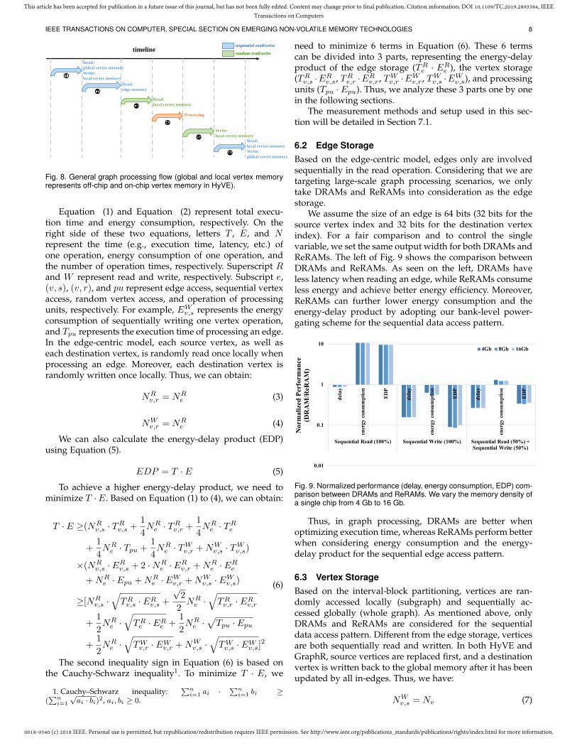
6.1 General ModelTwo main factors are involved in graph processing, execu-tion time and energy consumption, and these two factorslead to analysis of energy efficiency. We depict the graphprocessing flow in Fig. 8. As we can see, the whole graphprocessing flow can be divided into Step 1© to 6©. InStep 1©, vertex data are transferred from global memoryto local memory, which processing units can use for graphprocessing. In Step 2© to 5©, the graph algorithm is executedby reading an edge, reading the source/destination vertexvalue, updating, and writing the destination vertex value.Moreover, Step 2© to 5© can be executed simultaneously bypipelining. In Step 6©, vertex data are transferred from localmemory to global memory. Based on Fig. 8, we formalizethe execution time and energy consumption as follows:
T =NRv,s · TR
v,s
+NRe ·max(TR
v,r, TRe , Tpu, T
Wv,r)
+NWv,s · TW
v,s
≥NRv,s · TR
v,s
+1
4NR
e · TRv,r +
1
4NR
e · TRe +
1
4NR
e · Tpu +1
4NR
e · TWv,r
+NWv,s · TW
v,s(1)
E =NRv,s · ER
v,s
+2 ·NRv,r · ER
v,r +NRe · ER
e +NRe · Epu +NW
v,r · EWv,r
+NWv,s · EW
v,s(2)
0018-9340 (c) 2018 IEEE. Personal use is permitted, but republication/redistribution requires IEEE permission. See http://www.ieee.org/publications_standards/publications/rights/index.html for more information.
This article has been accepted for publication in a future issue of this journal, but has not been fully edited. Content may change prior to final publication. Citation information: DOI 10.1109/TC.2019.2893384, IEEETransactions on Computers
IEEE TRANSACTIONS ON COMPUTER, SPECIAL SECTION ON EMERGING NON-VOLATILE MEMORY TECHNOLOGIES 8
timeline
②
①
③
④
⑤
⑥
Read:
global vertex memory
Write:
local vertex memory
Read:
local vertex memory
Read:
edge memory
Write:
local vertex memory
Read:
local vertex memory
Write:
global vertex memory
Processing
sequential read/writesequential read/write
random read/writerandom read/write
Fig. 8. General graph processing flow (global and local vertex memoryrepresents off-chip and on-chip vertex memory in HyVE).
Equation (1) and Equation (2) represent total execu-tion time and energy consumption, respectively. On theright side of these two equations, letters T , E, and Nrepresent the time (e.g., execution time, latency, etc.) ofone operation, energy consumption of one operation, andthe number of operation times, respectively. Superscript Rand W represent read and write, respectively. Subscript e,(v, s), (v, r), and pu represent edge access, sequential vertexaccess, random vertex access, and operation of processingunits, respectively. For example, EW
v,s represents the energyconsumption of sequentially writing one vertex operation,and Tpu represents the execution time of processing an edge.In the edge-centric model, each source vertex, as well aseach destination vertex, is randomly read once locally whenprocessing an edge. Moreover, each destination vertex israndomly written once locally. Thus, we can obtain:
NRv,r = NR
e (3)
NWv,r = NR
e (4)
We can also calculate the energy-delay product (EDP)using Equation (5).
EDP = T · E (5)
To achieve a higher energy-delay product, we need tominimize T ·E. Based on Equation (1) to (4), we can obtain:
T · E ≥(NRv,s · TR
v,s +1
4NR
e · TRv,r +
1
4NR
e · TRe
+1
4NR
e · Tpu +1
4NR
e · TWv,r +NW
v,s · TWv,s)
×(NRv,s · ER
v,s + 2 ·NRe · ER
v,r +NRe · ER
e
+NRe · Epu +NR
e · EWv,r +NW
v,s · EWv,s)
≥[NRv,s ·
√TRv,s · ER
v,s +
√2
2NR
e ·√TRv,r · ER
v,r
+1
2NR
e ·√TRe · ER
e +1
2NR
e ·√Tpu · Epu
+1
2NR
e ·√TWv,r · EW
v,r +NWv,s ·
√TWv,s · EW
v,s]2
(6)
The second inequality sign in Equation (6) is based onthe Cauchy-Schwarz inequality1. To minimize T · E, we
1. Cauchy–Schwarz inequality:∑n
i=1 ai ·∑n
i=1 bi ≥(∑n
i=1
√ai · bi)2, ai, bi ≥ 0.
need to minimize 6 terms in Equation (6). These 6 termscan be divided into 3 parts, representing the energy-delayproduct of the edge storage (TR
e · ERe ), the vertex storage
(TRv,s ·ER
v,s, TRv,r ·ER
v,r , TWv,r ·EW
v,r, TWv,s ·EW
v,s), and processingunits (Tpu ·Epu). Thus, we analyze these 3 parts one by onein the following sections.
The measurement methods and setup used in this sec-tion will be detailed in Section 7.1.
6.2 Edge StorageBased on the edge-centric model, edges only are involvedsequentially in the read operation. Considering that we aretargeting large-scale graph processing scenarios, we onlytake DRAMs and ReRAMs into consideration as the edgestorage.
We assume the size of an edge is 64 bits (32 bits for thesource vertex index and 32 bits for the destination vertexindex). For a fair comparison and to control the singlevariable, we set the same output width for both DRAMs andReRAMs. The left of Fig. 9 shows the comparison betweenDRAMs and ReRAMs. As seen on the left, DRAMs haveless latency when reading an edge, while ReRAMs consumeless energy and achieve better energy efficiency. Moreover,ReRAMs can further lower energy consumption and theenergy-delay product by adopting our bank-level power-gating scheme for the sequential data access pattern.
0.01
0.1
1
10de
lay
ener
gy c
onsu
mpt
ion
EDP
dela
y
ener
gy c
onsu
mpt
ion
EDP
dela
y
ener
gy c
onsu
mpt
ion
EDP
Sequential Read (100%) Sequential Write (100%) Sequential Read (50%) +Sequential Write (50%)
Nor
mal
ized
Per
form
ance
(DR
AM
/ReR
AM
)
4Gb 8Gb 16Gb
Fig. 9. Normalized performance (delay, energy consumption, EDP) com-parison between DRAMs and ReRAMs. We vary the memory density ofa single chip from 4 Gb to 16 Gb.
Thus, in graph processing, DRAMs are better whenoptimizing execution time, whereas ReRAMs perform betterwhen considering energy consumption and the energy-delay product for the sequential edge access pattern.
6.3 Vertex StorageBased on the interval-block partitioning, vertices are ran-domly accessed locally (subgraph) and sequentially ac-cessed globally (whole graph). As mentioned above, onlyDRAMs and ReRAMs are considered for the sequentialdata access pattern. Different from the edge storage, verticesare both sequentially read and written. In both HyVE andGraphR, source vertices are replaced first, and a destinationvertex is written back to the global memory after it has beenupdated by all in-edges. Thus, we have:
NWv,s = Nv (7)

0018-9340 (c) 2018 IEEE. Personal use is permitted, but republication/redistribution requires IEEE permission. See http://www.ieee.org/publications_standards/publications/rights/index.html for more information.
This article has been accepted for publication in a future issue of this journal, but has not been fully edited. Content may change prior to final publication. Citation information: DOI 10.1109/TC.2019.2893384, IEEETransactions on Computers
IEEE TRANSACTIONS ON COMPUTER, SPECIAL SECTION ON EMERGING NON-VOLATILE MEMORY TECHNOLOGIES 9
Here, Nv is the number of vertices in a graph. However,the number of sequential reading times, NR
v,s, depends onthe partitioning and scheduling methods. In HyVE, thereare P
N super blocks (P is the number of intervals and Nis the number of processing units), and all correspondingvertices are loaded when processing a super block. Thus,we have:
NRv,s =
P
N·Nv (8)
In GraphR, graphs are processed in the step of 8 × 8blocks. When processing a block, 8 source vertices and 8destination vertices are loaded, and the total number ofvertices loaded depends on the number of nonempty blocks,Nnon−empty−blocks. Thus, in GraphR, we have:
NRv,s = 16 ·Nnon−empty−blocks (9)
As seen from Fig. 9, DRAMs achieve lower latencythan ReRAMs. However, the energy consumption and EDPdepends on the ratio between the number of reading andwriting times. Here, we show the EDP comparison betweenDRAMs and ReRAMs of HyVE and GraphR in Fig. 10.
0.1
1
10
YT WK AS LJ TW YT WK AS LJ TW
GraphR HyVE
Nor
mal
ized
ED
P(D
RA
M/R
eRA
M)
4Gb 8Gb 16Gb
Fig. 10. Normalized EDP comparison between DRAMs and ReRAMs onHyVE and GraphR. We vary the memory density of a single chip from 4Gb to 16 Gb.
Obviously, DRAMs achieve lower EDP in HyVE, whileReRAMs achieve better energy efficiency in GraphR. Thereason is that HyVE divides graphs into fewer partitions.Thus, the ratio between the number of reading and writingtimes in HyVE is less than that of GraphR. Thus, bothHyVE and GraphR adopt the memory with higher energyefficiency under their partitioning and scheduling methods.However, when we compare the total number of read-ing/writing vertices globally between HyVE and GraphR inFig. 11, we find that HyVE involves fewer vertices read thanGraphR. GraphR divides graphs into small partitions, andregister files are used for local random vertex access. Thus,in order to compare the performance of vertex memory, weneed to take both local and global memory into considera-tion.
The right of Fig. 11 shows the total delay, the energyconsumption, and an EDP comparison between GraphRand HyVE. Although GraphR adopts register files for localvertex access, which are faster (11.976 ps, 1.227 pJ for 32bit read; 10.563 ps, 1.209 pJ for writing) and consume lessenergy than SRAMs (2 MB; 960.03 ps, 23.84 pJ for 32 bit
0.001
0.01
0.1
1
10
100
1000
read
wri
te
dela
y
ener
gy c
onsu
mpt
ion
EDP
dela
y
ener
gy c
onsu
mpt
ion
EDP
Count DRAM ReRAM
Nor
mal
ized
Per
form
ance
(DR
AM
/ReR
AM
)
YT WK AS LJ TW
Fig. 11. Normalized performance comparison between HyVE andGraphR on vertex storage (GraphR/HyVE). We set DRAM/ReRAM den-sity of a single chip to 4 Gb, and SRAM size to 2 MB.
read; 557.089 ps, 24.74 pJ for 32 bit writing), HyVE stilloutperforms GraphR on delay, energy consumption, andEDP. The reason is that using register files requires dividinggraphs into small partitions, leading to more data transferbetween local and global vertex memory.
Thus, in graph processing, SRAMs are better for localrandom vertex access from the perspective of the wholevertex storage. When graphs are divided into a large num-ber of partitions, using DRAMs as global vertex memoryleads to higher energy efficiency and EDP, while ReRAMsare better when where are fewer partitions (e.g., HyVE afterdata sharing).
Moreover, dividing vertices into smaller partitions maylead to heavy preprocessing overheads, as shown in Sec-tion 6.5.
6.4 Processing Units
Two types of processing units, conventional CMOS circuits(adopted by HyVE) and ReRAM crossbars (adopted byGraphR) are compared in this section. In GraphR, an 8 × 8ReRAM crossbar is adopted to propagate the value of 8source vertices to 8 destination vertices. Assuming there areNavg edges in an 8 × 8 block, and the energy consumptionof a matrix vector multiplication operation on such ReRAMcrossbar is Ecb, the equivalent energy consumption of pro-cessing an edge should be:
Ecbpu =
Ecb
Navg(10)
We count Navg on five graphs (detailed in Section 7.1),and the result is shown in Table 1. Clearly, although graphshave been divided into 8 × 8 blocks (at most 64 edges ina block), there are only 1.23 to 2.38 edges in a block onaverage. Thus, the parallelism inside a crossbar is only 1.23to 2.38 on the datasets. On the other hand, small 8×8 blocksstill sparsely spread all over the graph.
Moreover, the precision of ReRAM cells is limited, andGraphR uses 4 crossbars with 4-bit cells to perform 16-bitoperations. Furthermore, to perform operations that are notbased on matrix vector multiplication, GraphR selects rowsin turn. Thus, the matrix vector multiplication operation isperformed 8 times in this situation. Consequently, the equiv-alent energy consumption of processing all edges should be:

0018-9340 (c) 2018 IEEE. Personal use is permitted, but republication/redistribution requires IEEE permission. See http://www.ieee.org/publications_standards/publications/rights/index.html for more information.
This article has been accepted for publication in a future issue of this journal, but has not been fully edited. Content may change prior to final publication. Citation information: DOI 10.1109/TC.2019.2893384, IEEETransactions on Computers
IEEE TRANSACTIONS ON COMPUTER, SPECIAL SECTION ON EMERGING NON-VOLATILE MEMORY TECHNOLOGIES 10
TABLE 1Average number of edges in non-empty 8× 8 blocks, graphs are from
Table 2.
Datasets Avg. edges in non-empty blocks (Navg)YT 1.44WK 1.23AS 2.38LJ 1.49
TW 1.73
Ecbpu,mv = 4 · Ecb
Navg(11)
Ecbpu,nmv = 8 · Ecb
Navg+ Eop (12)
Ecbpu,mv and Ecb
pu,nmv represent the equivalent energyconsumption of 16-bit matrix vector multiplication basedalgorithms (e.g., PageRank (PR)), and non matrix vectormultiplication based algorithms (e.g., Breadth-First Search).Eop in Equation (12) represents the energy consumptionof an operation in non matrix vector multiplication basedalgorithms (e.g., comparison in Breadth-First Search (BFS)).GraphR puts 8 operators at the output ports of each ReRAMcrossbar to perform these operations.
For conventional CMOS circuits-based processing units,the energy consumption of processing an edge is:
Ecmospu = Eop (13)
By comparing Ecmospu with Ecb
pu,nmv we can find thatusing CMOS circuits consumes less energy on BFS-like algo-rithms. The reason is that the operation is still performedby CMOS circuits at output ports of ReRAM crossbars inGraphR.
On the other hand, to perform a matrix vector multipli-cation operation on the ReRAM crossbar, we need to writeeach edge into the crossbar first, then a read operation isperformed in order to obtain the result. Thus, we can get:
Ecb = Navg · Erram,w + Erram,r (14)
and:
Ecbpu,mv = 4 · Erram,w + 4 · Erram,r
Navg(15)
Here, Erram,r and Erram,w represent the energy con-sumption of one read and write operation on the ReRAMcrossbar, respectively. We refer to GraphR [19] to obtainErram,w (3.91 nJ) and [34] to obtain Ecmos
pu (32-bit floatmultiplier, 3.7 pJ). We find thatErram,w > Ecmos
pu , leading toEcb
pu,mv > Ecmospu . Thus, using CMOS circuits also consumes
less energy on PR-like algorithms. The reason it that inorder to perform a matrix vector multiplication operationon the ReRAM crossbar, we need to write each edge tothe ReRAM crossbar first, and the energy consumptionof writing an edge to the ReRAM crossbar is larger thanperforming an operation on CMOS circuits.
The latency of processing units of GraphR when process-ing an edge is also shown as follows:
T cbpu,mv = Trram,w +
Trram,r
Navg(16)
We also refer to GraphR [19] and [35], and find thatthe latency of a CMOS 32-bit multiplier (18.783 ns) is lessthan the latency of writing an edge to the crossbar (Trram,w,50.88 ns). Moreover, the latency of a CMOS multiplier can befurther reduced by introducing pipelining. Thus, CMOS cir-cuits achieve less energy consumption and less latency thanReRAM crossbars, leading to lower EDP when processingan edge.
6.5 Preprocessing OverheadBoth HyVE and GraphR divide graphs into intervals andblocks, and they differ in the number of partitions. We testthe preprocessing time of dividing graphs into a differentnumbers of partitions on a physical machine (configurationwill be detailed in Section 7.1). The result is shown in Fig. 12,and the graphs used here are from Table 2.
00.250.50.751
1.25
Nor
mal
ized
spee
dup
# blocks
YT WK AS LJ TW
Fig. 12. Normalized preprocessing speed when the number of blocksvaries. Graphs are from Table 2
Obviously, the execution time of preprocessing is at thesame level when the number of blocks is small (e.g., ≤32×32). However, the execution time increases dramaticallywhen the number of blocks becomes larger (e.g., ≥ 64×64).Heavy overheads are introduced when addressing a largenumber of blocks in the memory.
Thus, in graph processing, dividing graphs into moreblocks leads to extra overheads, especially for a large num-ber of blocks.
6.6 Modeling Conclusion and Instructions for GraphProcessing on ReRAMsBased on the analysis above, we conclude instructions fordesigns of graph processing architectures on ReRAMs asfollows:
• Edge storage: For a global sequential edge readpattern and large data storage in graph processing,DRAMs achieve less latency, while ReRAMs performbetter on energy efficiency.
• Vertex Storage: For a local random vertex accesspattern, SRAMs perform better from the perspec-tive of whole vertex storage (execution time, energyconsumption, and energy efficiency). The choice be-tween DRAMs and ReRAMs for global vertex mem-ory depends on the number of partitions in a graph,

0018-9340 (c) 2018 IEEE. Personal use is permitted, but republication/redistribution requires IEEE permission. See http://www.ieee.org/publications_standards/publications/rights/index.html for more information.
This article has been accepted for publication in a future issue of this journal, but has not been fully edited. Content may change prior to final publication. Citation information: DOI 10.1109/TC.2019.2893384, IEEETransactions on Computers
IEEE TRANSACTIONS ON COMPUTER, SPECIAL SECTION ON EMERGING NON-VOLATILE MEMORY TECHNOLOGIES 11
and ReRAMs are better when there are not manypartitions.
• Using 8× 8 ReRAM crossbars may not achieve highparallelism inside the crossbar on real-world graphs.CMOS circuits perform better than the ReRAM cross-bar, from the perspective of processing an edge.
• Dividing graphs into more subgraphs leads to extraoverheads when there are more than thousands (>32× 32) of blocks.
Based on these conclusions for the memory hierarchyand the data access pattern in graph processing, we designHyVE. HyVE adopts better choices on every hierarchy thanGraphR (ReRAMs for edge storage, SRAMs+DRAMs forvertex storage when there are only a few partitions whenadopting data sharing in HyVE, and CMOS circuits foredge processing). Thus, HyVE can achieve higher energyefficiency than that of GraphR. Moreover, the preprocessingoverhead of HyVE is lighter than that of GraphR becauseHyVE divides graphs into fewer partitions.
Note that the analytic model in this section tries todecouple different memory/computing parts in our design(e.g., SRAM/DRAM for vertex memory, ReRAM for edgememory, CMOS for processing units, etc.), which explainsour choice of different memory devices for different partsin HyVE. However, no coupled parts exist, and the overallperformance will be shown in our experimental results inSection 7.
7 EVALUATIONS
7.1 Experiment SetupFive typical graph datasets shown in Table 2 are used for ourevaluation. PageRank (PR), Breadth-first Search (BFS), andConnected Components (CC) are the evaluated algorithms.The number of iterations for PR is set to 10 in our simulation,while for other two algorithms, the number of iterationsdepends on the graph data. Thus, we simulate them toconvergence. In one iteration, we traverse edges under theHyVE architecture. The source vertex value will be propa-gated to the destination vertex for updating. Because HyVEis general-purposed for different graph computation algo-rithms2, we do not apply a specific design for certain graphalgorithms (e.g., queue-based and read-based methods forBFS [36]).
TABLE 2Graph datasets used in evaluation
Datasets #Vertices #Edgescom-youtube (YT) 1.16 million 2.99 million
wiki-talk (WK) 2.39 million 5.02 millionas-skitter (AS) 1.69 million 11.1 million
live-journal (LJ) 4.85 million 69.0 milliontwitter-2010 (TW) 41.7 million 1,470 million
For the performance evaluation, we designed a customcycle-accurate simulator based on the single-board ver-sion of ForeGraph [18] (including accelerator logics andthe control group). We adopt 8 processing units in our
2. HyVE is not designed to support graph mining algorithms. [25]
HyVE design. The energy and timing models of SRAMand ReRAM were generated using NVSim [37] under the22 nm process. For the ReRAM cell, we set Read Voltageand Set Voltage to 0.4 V and 0.7 V, respectively. The ReadMode is current, with 0.16 µW Read Power. The Set Mode isvoltage, with 10 ns Set Pulse and 0.6 pJ Set Energy. The OnResistance at Read Voltage is 100 kΩ, and the Off Resistanceat Read Voltage is 10 MΩ. For the SRAM cell, the AccessCMOS Width is set to 1.31 F, with 146 F2 Cell Area. Otherparameters of ReRAM and SRAM are set to default, andwe will change memory models in our following experi-ments (e.g., total memory size, whether energy-optimized orlatency-optimized, leading to different memory parameterssuch as latency). The parameters of DRAM were generatedusing Micron System Power Calculators [38], with a defaultDDR4 SDRAM Configuration (e.g., Speed Grade is -093).The size of on-chip vertex memory is decided according tothe experimental results in Section 7.2.3, and the size of off-chip vertex memory and edge memory is linear with respectto the size of the dataset.
Since NVSim allows many optimization targets and con-figurations, different combinations are attempted to acquirethe most energy-efficient one (Table 3). We also use theIntel Processor Counter Monitor (PCM) [39] to measurethe performance on a hexa-core Intel i7 CPU running at3.3 GHz to demonstrate graph processing on conventionalCPU-based architecture. We run two software programson the CPU, and the first one is similar to NXgraph [12]except that all data is residented in the main memory in ourexperiments, while the onother is one is state-of-the-art inmemory graph processing systems, Galois [40].
7.2 Design Decisions
7.2.1 ReRAM Cell bits
A ReRAM cell can have more than two states in MLCchips. Since NVSim cannot model the behavior of an MLCReRAM chip, we made necessary modifications to NVSimaccording to the parallel sensing scheme [41] to calculate thepower and delay in MLC chips. With these parameters, oursimulator generates the results in Figure 13. Although MLCchips can increase the density and the internal bandwidth ofthe memory, extra sense amplifiers in MLC chips introducea nonnegligible amount of energy usage. Therefore, SLCoutperforms MLC in HyVE. Thus, SLC ReRAM is adoptedin later evaluations.
0200400600800
10001200
YT WK AS LJ TW
Ene
rgy
Eff
icie
ncy
(MT
EPS
/W)
1bit 2bits 3bits
Fig. 13. Energy efficiency (MTEPS/W) using different ReRAM cells.

0018-9340 (c) 2018 IEEE. Personal use is permitted, but republication/redistribution requires IEEE permission. See http://www.ieee.org/publications_standards/publications/rights/index.html for more information.
This article has been accepted for publication in a future issue of this journal, but has not been fully edited. Content may change prior to final publication. Citation information: DOI 10.1109/TC.2019.2893384, IEEETransactions on Computers
IEEE TRANSACTIONS ON COMPUTER, SPECIAL SECTION ON EMERGING NON-VOLATILE MEMORY TECHNOLOGIES 12
7.2.2 ReRAM Output BitsNVSim [37] provides diverse optimization models for agiven ReRAM design. To optimize the energy efficiency ofthe whole system, we compare two optimization directions,energy-optimize (minimize the energy consumption perread operation) and latency-optimize (minimize the work-ing period) in Table 3. We compare the energy efficiencyby joule per bit, which means the lowest power used toread one bit from ReRAM. The energy-optimized modelwith 512 bits output achieves the optimal energy efficiency3.Therefore, we choose this model in the following designs.
TABLE 3Power consumption under different bank configurations
energy(pJ)
period(ps)
power/bit(mW/bit)
energy-optimized
64bits 20.13 1221 0.26128bits 33.87 1983 0.13256bits 57.31 1983 0.11512bits 102.07 1983 0.10
latency-optimized
64bits 381.47 653 9.13128bits 378.57 590 5.01256bits 382.37 590 2.53512bits 660.23 527 2.45
7.2.3 SRAM CapacityTo evaluate the influence of variant SRAM sizes, we extractthe parameters from SRAM of capacity 4 MB, 8 MB, 16MB, and 32 MB and then simulate the energy efficiencyof HyVE. The result is shown in Table 4. Although thelarger capacity of SRAM reduces the data traffic betweenmemories, increasing the leakage power, read/write energyand delay have to be taken into consideration. In addition,the most efficient SRAM configuration is related to thesize of input graphs. For small datasets with small block
3. NVSim [37] can only provide simulation results for output bitssmaller than 512 bits.
numbers, such as YT, WK and AS, a 2 MB SRAM is sufficientto achieve high energy efficiency. For larger datasets, a 2 MBSRAM loses its advantage due to frequent data scheduling.However, when adopting data sharing scheme, a 2 MBSRAM achieves better energy efficiency in most cases. Inconclusion, for graph datasets with 1 M to 50 M vertices, a 4MB on-chip SRAM turns out to be the sweet spot for no datasharing configurations, while a 2 MB on-chip SRAM turnsout to be the sweet spot for data sharing configurations.
7.3 HyVE Performance
7.3.1 Data Sharing
HyVE reduces data transfer between on-chip and off-chipmemory by adopting the data sharing scheme among pro-cessing units. We use HyVE without using the data sharingscheme as the baseline. The experimental results in Fig. 14show that by adopting the data sharing scheme, HyVE canimprove the energy efficiency by 1.15x, 1.47x, and 2.19x(1.60x on average) on BFS, CC, and PR, respectively. The bitwidth of a vertex in the PR algorithm is wider than the othertwo algorithms, and the data sharing scheme reduces moredata transferring among local and global vertex memory,leading to the most benefits from adopting the data sharingscheme.
7.3.2 Bank Level Power-gating
HyVE adopts the aggressive bank-level power-gatingscheme by powering down most of the ReRAM banks. Wevalidated the improvement of energy efficiency introducedby such a scheme. The experimental results in Fig. 15 showthat the aggressive power-gating approach in HyVE yieldson average at 1.53x better results than acc+HyVE, whichdemonstrates the effectiveness of our power-gating design.The proportion is 2.00x if we compare HyVE with the powergating scheme of the acc+SRAM+DRAM configuration.
TABLE 4Energy efficiency varying SRAM sizes (MTEPS/W)
w/o power-gating, w/o sharing w/o power-gating, w/ sharing w/ power-gating, w/o sharing w/ power-gating, w/ sharing
2MB 4MB 8MB 16MB 2MB 4MB 8MB 16MB 2MB 4MB 8MB 16MB 2MB 4MB 8MB 16MB
BFS
YT 870 842 670 462 1001 851 677 505 1022 979 753 500 1207 991 762 551
AS 982 865 686 496 1044 869 689 515 1160 999 767 537 1248 1004 771 560
WK 754 833 663 448 959 844 672 500 875 971 747 485 1163 985 759 547
LJ 977 870 692 510 1048 874 693 519 1150 1002 772 552 1250 1007 774 563
TW 820 866 691 500 1006 873 693 518 947 997 770 541 1203 1006 774 562
CC
YT 641 807 644 414 901 823 658 488 738 948 731 448 1105 970 749 536
AS 793 850 675 472 981 857 681 508 920 985 757 512 1184 995 765 553
WK 454 754 632 393 793 790 649 480 511 893 720 425 985 945 742 529
LJ 772 853 681 479 983 863 687 512 889 986 762 517 1182 999 769 556
TW 480 826 674 445 845 851 686 507 535 955 754 478 1028 990 768 550
PR
YT 338 694 599 342 686 745 624 458 377 834 691 370 867 909 724 509
AS 486 795 654 431 827 821 665 494 547 932 739 467 1018 968 754 542
WK 170 610 534 233 472 687 585 410 185 742 622 249 609 860 693 460
LJ 435 803 657 412 804 834 673 495 483 935 739 443 986 977 760 541
TW 182 698 618 309 518 778 658 467 196 820 697 327 652 932 748 510

0018-9340 (c) 2018 IEEE. Personal use is permitted, but republication/redistribution requires IEEE permission. See http://www.ieee.org/publications_standards/publications/rights/index.html for more information.
This article has been accepted for publication in a future issue of this journal, but has not been fully edited. Content may change prior to final publication. Citation information: DOI 10.1109/TC.2019.2893384, IEEETransactions on Computers
IEEE TRANSACTIONS ON COMPUTER, SPECIAL SECTION ON EMERGING NON-VOLATILE MEMORY TECHNOLOGIES 13
1.0
1.5
2.0
2.5
3.0
BFS CC PR
Impr
ovem
ent
YT WK AS LJ TW
Fig. 14. Energy efficiency improvement by adopting data sharing inHyVE, compared with the configuration without using data sharingscheme (vertex data will be written back to the global vertex memoryfirst).
1.0
1.2
1.4
1.6
1.8
BFS CC PR
Impr
ovem
ent
YT WK AS LJ TW
Fig. 15. Energy efficiency improvement by adopting power-gating inHyVE.
7.3.3 Energy Efficiency of HyVE
We compare the energy efficiency results among differ-ent memory hierarchies, including acc+DRAM, acc+DRAM-opt, acc+ReRAM, acc+SRAM+DRAM, and acc+HyVE. Thedata scheduling in these four configurations is the same.The performance measured on the physical machine is con-sidered as the naive baseline. Here, we use two CPU-basedconfigurations as the baseline, CPU+DRAM (NXgraph inmemory) and CPU+DRAM-opt (Galois). The acc+DRAMconfiguration is the true baseline that demonstrates howmuch energy efficiency HyVE can improve by adopting thehybrid memory design. We run 8 threads on the physicalmachine, and use SET AFFINITY API to bind each threadto a certain physical core for NXgraph. For different graphdatasets, different partition numbers are used to fit into theSRAM. We also adopt two optimization methods above tothe acc+HyVE-opt configuration.
Fig. 16 shows the comparison results. Acc+HyVEachieves 1.51x, 3.10x, and 4.03x energy efficiency improve-ment on average over acc+SRAM+DRAM, acc+ReRAM,and acc+DRAM configurations, respectively. In ad-dition, acc+HyVE achieves 2 orders of magnitude(114.42x on average over CPU+DRAM, 83.31x on av-erage over CPU+DRAM-opt) improvement over theCPU-based baseline. Moreover, by adopting optimiza-tion methods, acc+HyVE-opt achieves 2.00x, 4.54x, 5.90x,and 145.71x energy efficiency improvement on averageover acc+SRAM+DRAM, acc+ReRAM, acc+DRAM, andCPU+DRAM configurations, respectively. Compared withthe baseline design using the accelerator, the optimized
1
10
100
1000
YT WK AS LJ TW
Energy efficiency running PR (MTEPS/W)
1
10
100
1000
10000
YT WK LJ TW
Energy efficiency running CC (MTEPS/W)
AS
CPU+DRAM-opt acc+SRAM+DRAM
1
10
100
1000
10000
YT WK AS LJ TW
Energy efficiency running BFS (MTEPS/W)
CPU+DRAM CPU+DRAM-opt acc+DRAM acc+ReRAM
acc+SRAM+DRAM acc+HyVE acc+HyVE-opt
Fig. 16. Energy efficiency (MTEPS/W) comparison between HyVE andother configurations.
HyVE can improve the energy efficiency by 5.90x, whilesimply using ReRAM to replace DRAM can only lead to1.31x energy efficiency improvement.
7.3.4 Energy Consumption BreakdownAs mentioned in Section 1, on-chip and off-chip mem-ory consumes more than 60% of the overall energy con-sumption in systems without HyVE. We illustrate theenergy consumption breakdown under three configura-tions, acc+SRAM+DRAM (SD), acc+HyVE (HyVE), andacc+HyVE+power-gating (opt) in Fig. 17. By adoptingReRAM in HyVE, the energy consumption of the wholememory system reduces by 57.57% and 86.17% under twoHyVE configurations compared with the SD configuration.The memory subsystem accounts for 75.68% and 52.91% ofthe total energy consumption in HyVE and opt, while thepercentage of SD is 88.62%. The obvious drop in the edgememory energy consumption is the main reason for theoverall energy savings. Thus, HyVE can significantly reducethe energy consumption in graph processing systems.
7.3.5 Absolute System PerformanceWe compare the execution time of acc+SRAM+DRAM (SD)and acc+HyVE to determine how HyVE can possibly in-fluence the absolute system performance. Fig. 18 shows

0018-9340 (c) 2018 IEEE. Personal use is permitted, but republication/redistribution requires IEEE permission. See http://www.ieee.org/publications_standards/publications/rights/index.html for more information.
This article has been accepted for publication in a future issue of this journal, but has not been fully edited. Content may change prior to final publication. Citation information: DOI 10.1109/TC.2019.2893384, IEEETransactions on Computers
IEEE TRANSACTIONS ON COMPUTER, SPECIAL SECTION ON EMERGING NON-VOLATILE MEMORY TECHNOLOGIES 14
0%
20%
40%
60%
80%
100%
YT
WK
AS
LJ
TW YT
WK
AS
LJ
TW YT
WK
AS
LJ
TW YT
WK
AS
LJ
TW YT
WK
AS
LJ
TW YT
WK
AS
LJ
TW YT
WK
AS
LJ
TW YT
WK
AS
LJ
TW YT
WK
AS
LJ
TW
SD HyVE opt SD HyVE opt SD HyVE opt
BFS CC PR
Other logic units Edge Memory Vertex Memory
Fig. 17. Energy consumption breakdown.
the normalized measurement data. It can be observed thatthere exists a slight increase of execution time if HyVE isadopted. The geometry mean of performance degradationfor the three tested algorithms are merely 1.9%, 2.5% and15.1%, respectively. It should be noted that the performanceresults are closely associated with design decisions of theselected ReRAM. Thus, with our choice of key parametersin the ReRAM modules, HyVE is able to yield profitable en-ergy efficiency results and incur no significant performancepenalty.
0.0
0.2
0.4
0.6
0.8
1.0
BFS CC PR
Abs
olut
e Pe
rfor
man
ce YT WK AS LJ TW
Fig. 18. Execution time comparison between SD and HyVE (SD/HyVE).
7.4 Comparison with GraphR
7.4.1 Preprocessing Overheads
As mentioned in Section 6.5, dividing graphs into more par-titions leads to extra preprocessing overheads. We comparethe execution time of preprocessing in HyVE and GraphR,and the result is shown in Fig. 19.
Clearly, by dividing graphs into fewer partitions, HyVEachieves 6.73x speedup during preprocessing comparedwith GraphR on average (the preprocessing time of GraphRis 6.73x longer than HyVE).
7.4.2 Dynamic Graph Support
As mentioned in Section 5, HyVE can support dynamicallyadding/deleting edges/vertices in graphs. We simulate thethroughput for dynamic graphs in Fig. 20. We also applythe same strategy for GraphR to support dynamic graphs.Tens of thousands of requests are issued in the simulation,and the proportion of adding edges, deleting edges, adding
0
2
4
6
8
10
YT WK AS LJ TW
Prep
roce
ssin
g tim
e (G
raph
R/H
yVE
)
Fig. 19. Preprocessing time comparison (GraphR/HyVE).
vertices, deleting vertices is 45%, 45%, 5%, 5%, respec-tively. The throughput is measured using millions of edgeschanged per second (adding/deleting vertices also resultsin changing edges).
0
10
20
30
40
50
YT WK AS LJ TW
Thr
ough
put
(mill
ion
edge
s)
HyVE GraphR
Fig. 20. Throughput of dynamically adding/deleting edges/vertices, sin-gle thread.
Obviously, HyVE can support up to 46.98 millions ofedges changed per second by adopting the method pro-posed in Section 5, which is 8.04x larger than that of GraphR.
7.4.3 Overall Performance
We compare the performance of GraphR and HyVE. We sim-ulate ReRAMs in GraphR according to the parameter pro-vided in its paper (The read/write latency and read/writeenergy cost used are 29.31 ns/50.88 ns and 1.08 pJ/3.91nJ respectively.). The results are shown in Fig. 21. We alsoadd two algorithms used in GraphR, Single Source ShortestPath (SSSP) and Sparse Matrix Multiplication (SpMV), inthis experiment.
Clearly, HyVE can is on average 5.12x faster thanGraphR, with 2.83x energy reduction on average, leadingto 17.63x lower EDP. The main reason is that in GraphR, anedge needs to be written to the ReRAM crossbar first beforeprocessing, and the energy consumption and latency of suchan operation is much larger than that on CMOS circuits.ReRAMs are good for performing computation locally at thememory, while the sparsity of graphs makes it impossibleto store graphs in the adjacent matrix format. Convertinggraphs from the edge list format to the adjacent matrix for-mat leads to heavy overheads, and it is inefficient to performonly one operation on each block after the conversion inGraphR.

0018-9340 (c) 2018 IEEE. Personal use is permitted, but republication/redistribution requires IEEE permission. See http://www.ieee.org/publications_standards/publications/rights/index.html for more information.
This article has been accepted for publication in a future issue of this journal, but has not been fully edited. Content may change prior to final publication. Citation information: DOI 10.1109/TC.2019.2893384, IEEETransactions on Computers
IEEE TRANSACTIONS ON COMPUTER, SPECIAL SECTION ON EMERGING NON-VOLATILE MEMORY TECHNOLOGIES 15
0.1
1
10
100
BFS CC PR
SSSP
SpM
V
BFS CC PR
SSSP
SpM
V
BFS CC PR
SSSP
SpM
V
delay energycomsumption
EDP
Nor
mal
ized
Per
form
ance
(G
raph
R/H
yve)
YT WK AS LJ TW
Fig. 21. Performance comparison between GraphR and HyVE.
8 CONCLUSION
In this paper, we present HyVE, a novel hybrid mem-ory hierarchy that consists of edge and vertex memory.HyVE takes advantage of ReRAM technology, and morearchitectural optimizations are also added to improve thegraph processing performance and energy efficiency. Theorganization of HyVE and a possible method to integrateHyVE with existing systems are discussed thoroughly. Wealso model the graph processing on ReRAMs from bothmemory and computation perspectives. ReRAMs are goodfor storing edges in graph processing for its low read en-ergy. However, using ReRAM crossbars in graph processingleads to heavy overheads because the latency and energyconsumption of writing an edge to the ReRAM crossbar ishigher than that of CMOS circuits. Thus, ReRAM crossbarsare not suitable for computation in graph processing if edgesare not stored in ReRAMs in the format of adjacent lists.Extensive experiments on various datasets show that HyVEcontributes more than 5.90x energy efficiency improvementscompared with common DRAM-based accelerators, and 2orders of magnitude improvement compared with the CPU-DRAM architecture. Moreover, HyVE can achieve 2.83xhigher energy efficiency than that of the previous ReRAM-based graph processing architecture. These results indicatethat HyVE is a promising solution for designing the memoryhierarchy of more efficient graph processing accelerators.
ACKNOWLEDGMENTS
This work was supported by National Key Research and-Development Program of China (No. 2017YFA0207600), Na-tional Natural Science Foundation of China (No.61373026,61832007, 61622403, 61621091). Guohao Dai is supported byChina Scholarship Council for his visiting at University ofCalifornia, Berkeley.
REFERENCES[1] Grzegorz Malewicz et al. Pregel: a system for large-scale
graph processing. In SIGMOD, pages 135–146. ACM, 2010.[2] Yucheng Low et al. Distributed GraphLab: a framework
for machine learning and data mining in the cloud. Pro-ceedings of the VLDB Endowment, 5(8):716–727, 2012.
[3] Joseph E Gonzalez et al. Powergraph: distributed graph-parallel computation on natural graphs. In OSDI, pages17–30. USENIX, 2012.
[4] Semih Salihoglu et al. GPS: a graph processing system. InSSDBM, page 22. ACM, 2013.
[5] Joseph E Gonzalez et al. GraphX: Graph processing in adistributed dataflow framework. In OSDI, pages 599–613.USENIX, 2014.
[6] Xiaowei Zhu et al. Gemini: A computation-centric dis-tributed graph processing system. In OSDI, pages 301–316.USENIX, 2016.
[7] Aapo Kyrola et al. GraphChi: Large-scale graph computa-tion on just a pc. In OSDI, pages 31–46. USENIX, 2012.
[8] Julian Shun et al. Ligra: a lightweight graph processingframework for shared memory. In ACM Sigplan Notices,volume 48, pages 135–146. ACM, 2013.
[9] Amitabha Roy et al. X-stream: Edge-centric graph process-ing using streaming partitions. In SOSP, pages 472–488.ACM, 2013.
[10] Wook-Shin Han et al. TurboGraph: a fast parallel graphengine handling billion-scale graphs in a single pc. InSIGKDD, pages 77–85. ACM, 2013.
[11] Xiaowei Zhu et al. GridGraph: Large-scale graph pro-cessing on a single machine using 2-level hierarchicalpartitioning. In ATC, pages 375–386. USENIX, 2015.
[12] Yuze Chi et al. NXgraph: an efficient graph processingsystem on a single machine. In ICDE, pages 409–420. IEEE,2016.
[13] Junwhan Ahn et al. A scalable processing-in-memoryaccelerator for parallel graph processing. In ISCA, pages105–117. IEEE, 2015.
[14] Tae Jun Ham et al. Graphicionado: A high-performanceand energy-efficient accelerator for graph analytics. InMICRO, pages 1–13. IEEE, 2016.
[15] Muhammet Mustafa Ozdal et al. Energy efficient archi-tecture for graph analytics accelerators. In ISCA, pages166–177. IEEE, 2016.
[16] Guohao Dai et al. FPGP: Graph processing framework onfpga a case study of breadth-first search. In FPGA, pages105–110. ACM, 2016.
[17] Tayo Oguntebi et al. Graphops: A dataflow library forgraph analytics acceleration. In FPGA, pages 111–117.ACM, 2016.
[18] Guohao Dai et al. ForeGraph: Exploring large-scale graphprocessing on multi-fpga architecture. In FPGA, pages217–226. ACM, 2017.
[19] Linghao Song et al. GraphR: Accelerating graph process-ing using ReRAM. In HPCA. IEEE, 2018.
[20] Mingxing Zhang et al. GraphP: Reducing communicationof pim-based graph processing with efficient data parti-tion. In HPCA. IEEE, 2018.
[21] Lei Han et al. A novel reram-based processing-in-memoryarchitecture for graph traversal. ACM TOS, 14(1):9, 2018.
[22] Mingyu Gao et al. Practical near-data processing for in-memory analytics frameworks. In PACT, pages 113–124.IEEE, 2015.
[23] J Joshua Yang et al. Memristive devices for computing.Nature nanotechnology, 8(1):13–24, 2013.
[24] Meng-Fan Chang et al. 19.4 embedded 1mb reram in 28nmCMOS with 0.27-to-1v read using swing-sample-and-couple sense amplifier and self-boost-write-terminationscheme. In ISSCC, pages 332–333. IEEE, 2014.
[25] Kai Wang et al. RStream: marrying relational algebra withstreaming for efficient graph mining on a single machine.In OSDI, pages 763–782. USENIX, 2018.
[26] Shijie Zhou et al. High-throughput and energy-efficientgraph processing on FPGA. In FCCM, pages 103–110.IEEE, 2016.
[27] Shyh-Shyuan Sheu et al. A 4Mb embedded slc resistive-ram macro with 7.2 ns read-write random-access timeand 160ns mlc-access capability. In ISSCC, pages 200–202.IEEE, 2011.
[28] Cong Xu et al. Overcoming the challenges of crossbar

0018-9340 (c) 2018 IEEE. Personal use is permitted, but republication/redistribution requires IEEE permission. See http://www.ieee.org/publications_standards/publications/rights/index.html for more information.
This article has been accepted for publication in a future issue of this journal, but has not been fully edited. Content may change prior to final publication. Citation information: DOI 10.1109/TC.2019.2893384, IEEETransactions on Computers
IEEE TRANSACTIONS ON COMPUTER, SPECIAL SECTION ON EMERGING NON-VOLATILE MEMORY TECHNOLOGIES 16
resistive memory architectures. In HPCA, pages 476–488.IEEE, 2015.
[29] Intel ivy bridge. https://www.7-cpu.com/cpu/IvyBridge.html.
[30] HP Labs. Cacti. http://www.hpl.hp.com/research/cacti/.[31] Guohao Dai et al. GraphH: A processing-in-memory
architecture for large-scale graph processing. IEEE TCAD,early access, 2018.
[32] Lawrence Page et al. The pagerank citation ranking:Bringing order to the web. Technical report, StanfordInfoLab, 1999.
[33] Jasmina Malicevic et al. Everything you always wanted toknow about multicore graph processing but were afraid toask. In ATC, pages 631–643. USENIX, 2017.
[34] Song Han et al. Learning both weights and connections forefficient neural network. In NIPS, pages 1135–1143, 2015.
[35] 32-bit floating-point multiplier. http://www.zipcores.com/datasheets/ieee mult.pdf.
[36] Sungpack Hong et al. Efficient parallel graph explorationon multi-core cpu and gpu. In PACT, pages 78–88. IEEE,2011.
[37] Xiangyu Dong et al. NVSim: A circuit-level performance,energy, and area model for emerging nonvolatile memory.IEEE TCAD, 31(7), 2012.
[38] Micron system power calculators. https://www.micron.com/support/tools-and-utilities/power-calc.
[39] Intel pcm. https://software.intel.com/en-us/articles/intel-performance-counter-monitor/.
[40] Donald Nguyen et al. A lightweight infrastructure forgraph analytics. In SOSP, pages 456–471. ACM, 2013.
[41] Cong Xu et al. Understanding the trade-offs in multi-levelcell ReRAM memory design. In DAC, pages 1–6. IEEE,2013.
Guohao Dai received his B.S. degree in 2014from Tsinghua University, Beijing. He is currentlypursuing the Ph.D. degree with the Departmentof Electronic Engineering, Tsinghua University,Beijing. His current research interests includeacceleration of large-scale graph processing onhardware and emerging devices, and virtualiza-tion techniques in the cloud. He has receivedBest Paper Award in ASPDAC 2019.
Tianhao Huang is currently a first-year PhDstudent in the MIT Computer Science and Arti-ficial Intelligence Lab. He joined the ComputerStructure Group in 2018. His research interestslie in the microprocessor and application-specifichardware accelerator design.
Yu Wang (S’05-M’07-SM’14) received his B.S.degree in 2002 and Ph.D. degree (with honor)in 2007 from Tsinghua University, Beijing. He iscurrently a tenured Professor with the Depart-ment of Electronic Engineering, Tsinghua Uni-versity. His research interests include brain in-spired computing, application specific hardwarecomputing, parallel circuit analysis, and pow-er/reliability aware system design methodology.
Dr.Wang has authored and coauthored over200 papers in refereed journals and confer-
ences. He has received Best Paper Award in ASPDAC 2019, FPGA2017, NVMSA 2017, ISVLSI 2012, and Best Poster Award in HEART2012 with 9 Best Paper Nominations (DATE18, DAC17, ASPDAC16,ASPDAC14, ASPDAC12, 2 in ASPDAC10, ISLPED09, CODES09). Heis a recipient of DAC under 40 innovator award (2018), IBM X10 FacultyAward (2010). He served as TPC chair for ICFPT 2019&2011, ISVLSI2018, Finance Chair of ISLPED 2012-2016, Track Chair for DATE 2017-2019 and GLSVLSI 2018, and served as program committee memberfor leading conferences in these areas, including top EDA conferencessuch as DAC, DATE, ICCAD, ASP-DAC, and top FPGA conferencessuch as FPGA and FPT.
Currently he serves as Co-Editor-in-Chief for ACM SIGDA E-Newsletter, Associate Editor for IEEE Transactions on CAD, IEEE Trans-actions on Circuits and Systems for Video Technology, Journal of Cir-cuits, Systems, and Computers, and Special Issue Editor for Microelec-tronics Journal. He also serves as guest editor for Integration, the VLSIJournal and IEEE Transactions on Multi-Scale Computing Systems. Hehas given 60+ invited talks in industry/academia. He is now with ACMDistinguished Speaker Program. He is an ACM/IEEE Senior Member.
Huazhong Yang (M’97-SM’00) was bornin Ziyang, Sichuan Province, P.R.China, onAug.18, 1967. He received B.S. degree inmicroelectronics in 1989, M.S. and Ph.D.degree in electronic engineering in 1993 and1998, respectively, all from Tsinghua University,Beijing.
In 1993, he joined the Department ofElectronic Engineering, Tsinghua University,Beijing, where he has been a Full Professorsince 1998. Dr. Yang was awarded the
Distinguished Young Researcher by NSFC in 2000 and Cheung KongScholar by Ministry of Education of China in 2012. He has beenin charge of several projects, including projects sponsored by thenational science and technology major project, 863 program, NSFC,9th five-year national program and several international researchprojects. Dr. Yang has authored and co-authored over 400 technicalpapers, 7 books, and over 100 granted Chinese patents. His currentresearch interests include wireless sensor networks, data converters,energy-harvesting circuits, nonvolatile processors, and brain inspiredcomputing. Dr. Yang has also served as the chair of Northern ChinaACM SIGDA Chapter.
John Wawrzynek (M’85) received the B.S. de-gree in electrical engineering from the State Uni-versity of New York at Buffalo, Buffalo, the M.S.,Ph.D. degrees in computer science from the Cal-ifornia Institute of Technology, Pasadena, andthe M.S. degree in electrical engineering fromthe University of Illinois at Urbana-Champaign,Urbana.
He is currently a Professor of Electrical Engi-neering and Computer Sciences with the Univer-sity of California, Berkeley. He is a Faculty Scien-
tist with the Lawrence Berkeley National Laboratory, Berkeley, CA, andis a Co-Director with the Berkeley Wireless Research Center, Berkeley.He was a Co-Founder of Andes Networks, Inc., Mountain View, CA,and of BEECube, Inc., Fremont, CA, two companies specializing in ac-celerators and reconfigurable computing systems. His current researchinterests include reconfigurable computing and computer architecture.