impedance spectroscopy for manufacturing control … · impedance spectroscopy for manufacturing...
TRANSCRIPT

Impedance Spectroscopy for Manufacturing Control of
Material Physical Properties
Xiaobei Li
A thesis submitted in partial fulfillment of the requirements for the degree of
Master of Science in Electrical Engineering
University of Washington 2003
Program Authorized to Offer Degree: Department of Electrical Engineering

University of Washington
Graduate School
This is to certify that I have examined this copy of a master’s thesis by
Xiaobei Li
and have found that it is complete and satisfactory in all respects,
and that any and all revisions required by the final
examining committee have been made.
Committee Members:
_________________________________________
Alexander Mamishev
_________________________________________
Lloyd Burgness
_________________________________________
Karl Böhringer
Date: _________________

In presenting this thesis in partial fulfillment of the requirements for a Master’s degree at
the University of Washington, I agree that the Library shall make its copies freely
available for inspection. I further agree that extensive copying of this thesis is allowable
only for scholarly purposes, consistent with "fair use" as prescribed in the U.S. Copyright
Law. Any other reproduction for any purposes or by any means shall not be allowed
without my written permission.
Signature_______________________________
Date___________________________________

University of Washington
Abstract
Measuring Physical Properties of Organic Materials Using Dielectric Spectroscopy
by Xiaobei Li
Chairperson of the Supervisory Committee
Assistant Professor Alexander Mamishev
Department of Electrical Engineering
Real-time non-invasive sensing techniques are needed for online process control
in manufacturing industries. Impedance spectroscopy is a powerful sensing tool that can
be used for real-time non-invasive process parameter control. Applications currently
under investigation in this thesis involve moisture content sensing in food and
pharmaceutical products, and hardness and coating thickness evaluation for
pharmaceutical samples. A self-containing data acquisition and sensor control system is
designed for these applications. The system is able to perform real-time capacitance and
conductance measurements, and process the data to obtain parameters of interest. The
system can be calibrated according to the requirement of each application and can be
integrated into the feedback loop of the corresponding process control system. System
calibration involves establishing a one-to-one mapping between the parameters of interest
and the measured material impedance. The effect of other parameters needs to be
eliminated or accounted for. Experimental data demonstrates good sensitivity to
parameter variation. After compensation for disturbance factors, such as moisture
diffusion, a nearly linear dependency is observed between cookie dough moisture content
and the measured sample impedance. The investigation in pharmaceutical applications is
still at a preliminary stage. Experimental results indicate the feasibility for a broad

application of this technique in the pharmaceutical industry. A large amount of
experiments need to be conducted for a comprehensive calibration process.

i
Table of Contents
List of Figures .................................................................................................................... iv
List of Tables .................................................................................................................... vii
Chapter 1. Introduction................................................................................................. 1
1.1. Background..................................................................................................... 1
1.2. Motivation....................................................................................................... 1
1.3. State of the art ................................................................................................. 2 1.3.1 Techniques for measuring material properties........................................................................2 1.3.2 Dielectrometry sensing............................................................................................................2
1.4. Outline of this thesis ....................................................................................... 3
Chapter 2. Basics of dielectrometry sensing ................................................................ 5
2.1. Introduction to the theory of dielectrics.......................................................... 5
2.2. Principle of dielectric spectroscopy sensing ................................................... 6 2.2.1 Sensing possibilities.................................................................................................................6 2.2.2 Impedance spectroscopy and dielectric spectroscopy .............................................................7 2.2.3 Calibration based sensing .......................................................................................................8 2.2.4 Differential sensing .................................................................................................................8 2.2.5 Imaging – electrical impedance tomography (EIT).................................................................8
2.3. From parallel plate sensors to fringing field sensors .................................... 11
2.4. Penetration depth .......................................................................................... 12
2.5. Disturbance factors ....................................................................................... 13 2.5.1 Surface contact quality ..........................................................................................................13 2.5.2 Stray capacitances.................................................................................................................14 2.5.3 Deviation from ideal finite element analysis model...............................................................15 2.5.4 Interfacial double layer effect................................................................................................16
Chapter 3. Interdigital Fringing Field Dielectrometry................................................ 18
3.1. Overview of the measurement system .......................................................... 18
3.2. Fringing electric field sensor design ............................................................. 20 3.2.1 Figures of merit .....................................................................................................................20 3.2.2 Major design concerns ..........................................................................................................23 3.2.3 Example of multi-channel fringing field sensor designs........................................................27

ii
3.3. Sensor interface circuit ................................................................................. 35
Chapter 4. Moisture dynamics in cookies .................................................................. 38
4.1. Definition of the problem.............................................................................. 38
4.2. Methodology................................................................................................. 39
4.3. Experimental setup........................................................................................ 39 4.3.1 The Concentric Sensor Head.................................................................................................39 4.3.2 A Voltage Divider Circuit......................................................................................................41
4.4. Experimental procedure ................................................................................ 42
4.5. Experimental result and data analysis........................................................... 42 4.5.1 Compensation for Moisture Diffusion ...................................................................................43 4.5.2 Linear Regression..................................................................................................................44 4.5.3 Compensation for Non-Uniform Air Gap ..............................................................................45 4.5.4 Moisture Content Distribution...............................................................................................45 4.5.5 Evaluation of the Calibration Model.....................................................................................46
4.6. The effect of temperature variation............................................................... 47 4.6.1 The double layer effect ..........................................................................................................49 4.6.2 Lumped circuit simulation .....................................................................................................49
4.7. Simulating the manufacturing process – the rotating table........................... 52
4.8. The chemometric challenge – temperature and moisture control chamber .. 52
4.9. Conclusions................................................................................................... 53
Chapter 5. Measuring Physical Properties of Pharmaceutical Samples ..................... 54
5.1. Problem statement......................................................................................... 54
5.2. Motivation..................................................................................................... 54
5.3. Measuring tablet hardness and coating thickness ......................................... 55 5.3.1 Information on sample physical properties ...........................................................................55 5.3.2 Experimental setup ................................................................................................................56 5.3.3 Experimental results ..............................................................................................................57
5.4. Measuring tablet coating thickness............................................................... 58 5.4.1 The experimental setup..........................................................................................................58 5.4.2 The experimental results – parallel plate ..............................................................................59 5.4.3 The experimental results – fringing field...............................................................................62

iii
5.5. Acquiring drug signature using a FEF sensor............................................... 65
5.6. Choice of sensors – FEF vs. parallel plate.................................................... 67
5.7. Measuring API concentration for powder samples....................................... 69
5.8. Conclusion and future work.......................................................................... 71
Chapter 6. Conclusions and future work .................................................................... 73
6.1. Conclusions................................................................................................... 73
6.2. Directions of future work.............................................................................. 73 6.2.1 Information decoupling for multivariable experiments .........................................................73 6.2.2 More sophisticated parameter estimation algorithms ...........................................................73 6.2.3 Statistical evaluation of experimental results........................................................................74
End notes........................................................................................................................... 75
References......................................................................................................................... 80
Appendix........................................................................................................................... 85
1. DiSPEC hardware installation guide ............................................................ 85
2. DiSPEC software guide ................................................................................ 91

iv
List of Figures
Figure Number Page
2.1. Flow diagram of the dielectrometry system................................................................. 7
2.2. Transition from parallel plate geometry to in-plane fringing field geometry............ 11
2.3. A guard ring parallel plate capacitor.......................................................................... 11
2.4. Interdigital fringing electric field sensor with spatial wavelength λ.......................... 12
2.5. Cross-section view of a fringing electric field sensor................................................ 13
2.6. Maxwell simulation layout of a sample positioned above an interdigital sensor. ..... 15
2.7. Illustration of the double layer effect......................................................................... 16
3.1. Diagram of the measurement system......................................................................... 18
3.2. Labview device control and data acquisition interface.............................................. 19
3.3. Three-channel sensor interface circuit. ...................................................................... 20
3.4. Sensor interface circuit schematics. .......................................................................... 20
3.5. Maxwell simulation result of an interdigital fringing field sensor. ........................... 22
3.6. Transparent sensor ..................................................................................................... 25
3.7. Maxwell simulation results of a concentric-ring fringing field setup........................ 27
3.8. Three-wavelength fringing electric field sensor. ....................................................... 28
3.9. Three-wavelength fringing electric field sensor. ....................................................... 29
3.10. Top down view of a concentric fringing field sensor head...................................... 30
3.11. Top down view of a shielded concentric fringing field sensor head. ...................... 30
3.12. Maxwell simulation layout of a sample above the concentric FEF sensor.............. 31
3.13. Normalized capacitance measurement from the inner sensing channel .................. 32
3.14. Normalized capacitance measurement from the outer sensing channel .................. 32
3.15. The effect of the addition of shielding electrodes.................................................... 33
3.16. Maxwell simulation results of the two concentric fringing field sensor.................. 34
3.17. Normalized capacitance data from the simulation results of Maxwell.................... 34
3.18. A couple of novel designs........................................................................................ 35
3.19. Floating voltage with ground. .................................................................................. 36
3.20. Floating voltage with guard. .................................................................................... 36

v
4.1. Top and bottom view of the concentric sensor head.................................................. 39
4.2. Side view of the sensor in a voltage divider setup..................................................... 40
4.3. Detailed circuit model considering double layer effect. ............................................ 41
4.4. Sensor geometry and experimental setup. ................................................................. 42
4.5. Capacitances measured at different moisture content levels. .................................... 43
4.6. Phase measurements at different moisture content levels.......................................... 43
4.7. Capacitance measurements against the mass of added water at 10 kHz.................... 44
4.8. Moisture content distribution across the radius of the sample .................................. 46
4.9. Moisture loss dynamics of the cookie dough sample. ............................................... 48
4.10. Capacitance measurements of cookie dough sample............................................... 48
4.11. Phase measurements of cookie dough sample against sample surface temperature.49
4.12. Lumped circuit model for the double layer effect. .................................................. 50
4.13. Frequency dependency of the lumped circuit model. .............................................. 51
4.14. Frequency dependency of the lumped circuit model. .............................................. 51
4.15. The rotating table setup............................................................................................ 52
4.16. Moisture and temperature control chamber. ............................................................ 53
5.1. Photo of the pharmaceutical samples used in the experiments.................................. 55
5.2. Tablet sample weight and thickness against sample pressure. .................................. 56
5.3. Capacitance measurements of 180 mg tablet samples against sample hardness. ...... 58
5.4. Phase measurements of 180 mg tablet samples against sample hardness. ................ 58
5.5. Fringing electric field sensor setup for measuring tablet coating thickness. ............. 59
5.6. Absolute capacitance measurements from a parallel plate sensor. ............................ 60
5.7. Capacitance variation measurement from the parallel plate setup............................. 60
5.8. Phase variation measurement from the parallel plate setup....................................... 61
5.9. Capacitance variation against sample weight using a parallel plate sensor............... 61
5.10. Absolute capacitance measurements from the FEF setup........................................ 63
5.11. Capacitance variation from a FEF sensor with spatial wavelengh of 500 µm......... 63
5.12. Phase variation from a FEF sensor with spatial wavelengh of 500 µm................... 64
5.13. Capacitance variation against sample weight. ......................................................... 64
5.14. Fringing electric field sensor setup for acquiring drug signature. ........................... 65
5.15. Capacitance measurements from a FEF sensor. ...................................................... 66
vi
5.16. Phase measurements from a FEF sensor with spatial wavelength of 500 µm. ........ 66
5.17. Normalized capacitance from the parallel plate setup. ............................................ 68
5.18. Normalized capacitance from the frining field setup............................................... 69
5.19. Capacitance measurements of powder samples of various drying time. ................. 70
5.20. Phase measurements of powder samples of various drying time. ........................... 71
5.21. Capacitance measurements of powder samples against sample drying time........... 71

vii
List of Tables
Table Number Page
4.1 Comparison between actual moisure and added moisture.......................................... 47
5.1. Tablet sample physical properties: hardness, weight, thickness................................ 56

viii
Acknowledgments
The previous one and half years of research experience at SEAL has been very
pleasant, thanks to my advisor, Prof. Alexander Mamishev, who is very understanding
and fun to work with. The thesis would not have been possible without his consistent
guidance and support.
I am also very grateful towards my lab mates, Michael for proofreading the thesis,
Kishore for providing some of the experimental data, Alexei for the many interesting
discussions and ideas we shared, Sam for the contribution in sensor design, Henry and Yu
cheung for help with software development, and Kelly and Chika for running the
Maxwell simulations.
I would also like to acknowledge the financial support from Kraft foods for the
moisture sensing project. I am especially grateful to Dr. Carol Zrybko and Dr. Robert
Magaletta, for their help and advice on the project.

1
Chapter 1. Introduction
1.1. Background Dielectrometry is widely used for determination of material physical properties due to its
non-invasiveness and wide spectrum of sensing possibilities. Applications include
agricultural products [1], soil [2], paper [3], transformer board [4], biological sensing
[5,6] and hydrophilic polymers [7].
Capacitive sensors are often used for dielectric spectroscopy. They have the
advantage of high measurement accuracy and non-invasiveness. The simplest examples
of capacitive sensors are a guard-ring parallel-plate capacitor and a coaxial cylindrical
capacitor. More complicated examples include fringing electric field sensors, which can
assume various geometries [8,9]. The penetration depth of fringing electric field sensors
is proportional to the distance between coplanar electrodes. By applying different voltage
patterns to the sensor, variable penetration depths can be achieved, thus providing FEF
sensors access to different layers of the material. This characteristic, combined with their
one-sided access capability, makes FEF sensors more flexible in use than their parallel-
plate counterparts.
1.2. Motivation Lack of control in industrial processes limits the productivity of the manufacturers. Real-
time, non-invasive sensing systems are needed for feedback control of the parameters of
interest, such as moisture content, texture, hardness, and viscosity. This need has driven
many advances in the field of dielectrometry. This thesis discusses an impedance
spectroscopy technique, where functional dependencies between material properties of
interest and electrical impedance measurements are determined empirically and used to
calibrate the sensing system. The major challenge of this technique is to achieve
selectivity for the sensing system. Material properties other than those of interest are
usually considered to be disturbance factors, the effects of which have to be accounted
for in the parameter estimation algorithm. Other challenges include optimization of
sensor geometry for the particular application and inverse problem solving.

2
1.3. State of the art
1.3.1 Techniques for measuring material properties
1.3.1.1 NMR and MRI There has been extensive application of NMR and MRI techniques in bio-sensing and
medical imaging. Compared with other imaging techniques such as X-ray, NMR and
MRI have the advantage of non-invasiveness. Applications of NMR and MRI to food
product sensing have also been developed [10,11], especially in the field of food imaging
[12-16]. Although these techniques offer high measurement accuracy, so far they are not
fit for real time control industrial applications due to their high cost.
1.3.1.2 Ultrasound sensing Another popular technique in the field of bio-sensing and medical imaging is ultrasound.
Extensive study has been done in this direction. Other applications of ultrasound
technology include monitoring the curing process of resin [17].
1.3.2 Dielectrometry sensing Most industrial applications do not have high accuracy requirements, while production
cost needs to be kept as low as possible. Compared with the sensing technologies
mentioned above, dielectrometry sensing does not require special, high-caliber
measurement devices. This offers dielectrometry sensing techniques great flexibility to be
integrated into the manufacturing control processes.
1.3.2.1 Microwave and RF sensing Microwave and RF spectroscopy techniques are available for non-invasive sensing of
materials properties. They have been used for sensing the property of agricultural
products [1] as well as food products [18]. Near infrared spectroscopy is widely
employed for a number of qualitative studies as well as quantitative analysis of material
properties. The spectral region investigated by NIR covers the wavelength range from
700 nm to about 2500 nm. Applications of NIR spectroscopy include moisture content
determination for impregnated paper [19].

3
1.3.2.2 Dielectrometry sensing of food products Despite the advantage of low cost, applications of dielectrometry sensing to food
products are relatively scarce than those of NMR and MRI. Applications already under
investigation include evaluation of dielectric property of the biscuit dough [20] and
imaging of the cooking process of bread samples [16].
1.3.2.3 Dielectrometry sensing of pharmaceutical products Although the technique of dielectrometry sensing has existed for a long time, its
application to the pharmaceutical industry is very recent. Applications already under
investigation include bioahesive gels [21], measurement of solids, detection of inter-batch
variation, measurement of emulsions and lipsome suspensions, the characterization of
proteins and biomolecules [22], the evaluation of thermal aging effect in pharmaceutical
systems [23].
1.3.2.4 Microdielectrometry Microdielectrometry was first proposed by Senturia [24]. Since then great advances have
taken place in the field MEMS, the prospect of a low-cost, power-efficient, and
disposable mini-sensor is no longer just a distant dream. However, the field of
microdielectrometry sensing has been relatively stagnant. There are some recent efforts
of applying microdielectrometry to bio-sensing. Dielectrometry sensors at MEMS scale
allow us to study the physical properties of individual cells. Another potential application
is in the study of sensitive skin, where each dielectrometry sensor cell simulates a neuron
of the human body [25].
1.4. Outline of this thesis Chapter 1 provides the state of art for dielectrometry sensing and its applications. Chapter
2 gives an overview on the basics of the dielectrometry theory. A brief description and
comparison between impedance spectroscopy, dielectric spectroscopy, and electric
impedance tomography is provided. Fundamentals of fringing electric field sensing are
also provided. Chapter 3 talks about the various aspects of experimental setup design,
which include sensor design, interface circuit design, and the circuit calibration
4
algorithm. A special focus is placed on multi-channel fringing electric field sensor
design, yet some of the issues addressed in this chapter apply to all types of sensor
geometries. Chapter 4 focuses on parameter estimation algorithms. The forward and the
inverse problem are defined in this chapter. Algorithms for disturbance factor
compensation are also discussed. Chapter 5 and 6 deal with the experimental results and
data analysis from the cookie dough and pharmaceutical applications respectively.

5
Chapter 2. Basics of dielectrometry sensing
2.1. Introduction to the theory of dielectrics
Materials are usually divided into the categories of conductors, insulators, and dielectrics.
Dielectric materials cover the whole spectrum of anything between conductors and
insulators. Dielectrics consist of polar molecules, or non-polar molecules, or very often
both. Due to the asymmetric configuration of polar molecules, material consisting of
these molecules has built-in dipole moments. Under an external electric field, the
polarized dipoles reorient in the electric field and neutralize some of the charges on the
electrodes. The most often used measure of material dielectric properties is the complex
dielectric permittivity. It is a measure of the ability of the dielectric material to reorient
and neutralize charges on the electrodes. This usually depends on how polarized the
material is and the inertial force it has to overcome to reorient. Sometimes, relative
complex dielectric permittivity is used to describe material dielectric properties. It is
defined as the ratio between the dielectric permittivity of the material and that of free
space. The dielectric permittivity of free space is 128.85 10 /F m−× .
The dielectric permittivity of most dielectric materials is frequency-dependent. In the
presence of an alternating electric field, the dipole moments inside the material oscillates
with the direction of the electric field. The higher the frequency the harder it is for the
dipole moments to catch up with the change of field direction. This results in a decreasing
ability of the material to neutralize charges on the electrodes at high frequencies. In
general, the total complex dielectric permittivity ε*(ω) is written as:
*( ) '( ) ''( )iε ω ε ω ε ω= −
(2.1)
where 'ε and ''ε are, respectively, the real permittivity and the dielectric loss factor of
the material.
Jonscher of the Chelsea Dielectric Group has been studying the problem of a
universal relaxation law [26]. But till now, no one has proved the existence of a general
model to describe the dielectric relaxation process. One of the most widely used models
for fitting dielectric relaxation data is the Havriliak-Negami (HN) function, as shown in

6
(2.2), where 0ε is the dielectric permittivity at dc and ε∞ is its asymptotic value at
infinite high frequency. The term 0ε ε∞− is the total dielectric relaxation strength and 0τ
is the relaxation time of the material. For 1β = , the Cole-Cole model emerges; whereas
for 1α = the Davison-Cole model emerges.
( )
0
0
*( )1 i
βα
ε εε ω εωτ
∞∞
−= +
+ (2.2)
''σ ωε=
(2.3)
2.2. Principle of dielectric spectroscopy sensing
2.2.1 Sensing possibilities
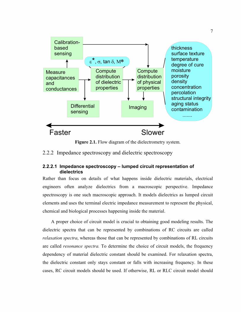
Dielectrometry is one of the most versatile sensing techniques. Figure 2.1 shows the flow
diagram of a dielectrometry system. Material dielectric permittivity is dependent on
various material physical properties such as geometry, texture, temperature, degree of
cure, moisture content and aging status. Changes in these physical properties will be
reflected as changes in such dielectric property variables as *ε ,σ , and tanδ , where σ is
defined in (2.3) and tanδ is defined as the ratio between the real and imaginary part of
the complex impedance. These parameters variations, in turn, lead to changes in the
impedance measurements from the sensor. The fact that dielectric measurements are
sensitive to changes of a wide range of material physical properties makes dielectrometry
sensing technique a potential candidate for a broad spectrum of sensing applications.
7
Measurecapacitancesand conductances
Calibration-basedsensing
Differentialsensing
Computedistributionof dielectricproperties
Computedistributionof physicalproperties
Imaging
Faster Slower
ε σ, δ, Μ*, tan ∗
thicknesssurface texturetemperaturedegree of curemoistureporositydensityconcentrationpercolationstructural integrityaging statuscontamination .......
Figure 2.1. Flow diagram of the dielectrometry system.
2.2.2 Impedance spectroscopy and dielectric spectroscopy
2.2.2.1 Impedance spectroscopy – lumped circuit representation of dielectrics
Rather than focus on details of what happens inside dielectric materials, electrical
engineers often analyze dielectrics from a macroscopic perspective. Impedance
spectroscopy is one such macroscopic approach. It models dielectrics as lumped circuit
elements and uses the terminal electric impedance measurement to represent the physical,
chemical and biological processes happening inside the material.
A proper choice of circuit model is crucial to obtaining good modeling results. The
dielectric spectra that can be represented by combinations of RC circuits are called
relaxation spectra, whereas those that can be represented by combinations of RL circuits
are called resonance spectra. To determine the choice of circuit models, the frequency
dependency of material dielectric constant should be examined. For relaxation spectra,
the dielectric constant only stays constant or falls with increasing frequency. In these
cases, RC circuit models should be used. If otherwise, RL or RLC circuit model should
8
be used [27].
In addition to lumped circuit models, distributed circuit models are sometimes used
to model dielectric materials as a distributed dielectric medium in bounded or unbounded
space [28,29].
2.2.2.2 Dielectric spectroscopy Dielectric spectroscopy relates material dielectric properties with corresponding physical
properties and investigates the fundamental theoretical link between them. For industrial
applications, where in-depth theoretical knowledge of material nature is unnecessary,
impedance spectroscopy is sufficient. Dielectric spectroscopy is often used for research
efforts investigating material dielectric properties.
2.2.3 Calibration based sensing
Calibration based sensing works by establishing a quantitative relationship between
material physical property of interest and the resulting impedance measurements. This
functional dependence is usually empirically determined. Very often a linear dependency
is assumed. The algorithms for such calibration-based approaches are usually quite
straightforward, yet these approaches are not sufficient to gain insight about the physical
nature of the material and the calibration parameters are always subject to changes when
a different setup is adopted.
2.2.4 Differential sensing
Differential sensing works by scanning over the test specimen and analyzing the
measurement variation at different locations. This sensing technique provides fast
relative information about the material under test. It is suitable for industrial monitoring
applications, where speed is important and high measurement accuracy is not required.
2.2.5 Imaging – electrical impedance tomography (EIT)
For inhomogeneous materials, interest exits to look at the distribution of the dielectric
and physical properties of the material. EIT is one of the most widely used technologies
9
for such applications. Applications of EIT include bio-sensing, medical imaging,
geophysics sensing, and industrial process control.
Compared with other tomography and imaging techniques, EIT is relatively
inexpensive, which makes it a popular choice for industrial applications. However, unlike
X-ray or laser imaging, EIT is the “soft field” technique in which the field lines that
penetrate through the material do not stay in a straight path. This makes the parameter
estimation algorithms for EIT much more challenging than those for other techniques.
Compared with differential sensing and calibration based sensing, EIT and other
such imaging techniques are usually slower, due to the high computation complexity
involved in the parameter estimation algorithms.
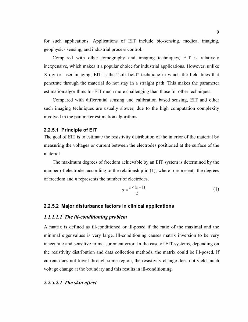
2.2.5.1 Principle of EIT The goal of EIT is to estimate the resistivity distribution of the interior of the material by
measuring the voltages or current between the electrodes positioned at the surface of the
material.
The maximum degrees of freedom achievable by an EIT system is determined by the
number of electrodes according to the relationship in (1), where α represents the degrees
of freedom and n represents the number of electrodes.
( 1)2
n nα × −= (1)
2.2.5.2 Major disturbance factors in clinical applications
1.1.1.1.1 The ill-conditioning problem
A matrix is defined as ill-conditioned or ill-posed if the ratio of the maximal and the
minimal eigenvalues is very large. Ill-conditioning causes matrix inversion to be very
inaccurate and sensitive to measurement error. In the case of EIT systems, depending on
the resistivity distribution and data collection methods, the matrix could be ill-posed. If
current does not travel through some region, the resistivity change does not yield much
voltage change at the boundary and this results in ill-conditioning.
2.2.5.2.1 The skin effect
10
The skin effect is a major disturbance factor for clinical applications of EIT. The skin is
composed of layers of dead cells. At low frequency, the impedance of unabraded skin can
be as high as 1 MΩ/cm2. Its impedance decreases if the dead skin on the surface is
scraped off. The existence of this huge shunt impedance makes it very difficult to
measure the internal distribution of resitivity accurately. Phantoms are usually used to
calibrate and evaluate imaging systems like EIT. However, it is very difficult to find a
physical analog to model human skin in the phantom, namely a thin layer of material with
high impedance. Polyimide comes closest to the requirement, but is still not good enough.
One solution to this problem is to move from the two-electrode setup to the four-
electrode setup, where current is injected through one pair of electrodes and voltage
measured from another pair of electrodes, thus reducing the effect of skin impedance.
The four-electrode setup is obviously more complicated than the two-electrode one. For
applications where only differential sensing is of interest and absolute measurement
accuracy is not required, such as those applications in geophysics, the two-electrode setup
is often used.
Another solution is to inject current from multiple pairs of electrodes. This is called
multi-reference approach. The skin effect is less pronounced in this case due to the
relatively large supply current.
2.2.5.2.2 Electrode position
One major source of uncertainty for EIT systems is the electrode position. Information on
the exact position of the electrodes is necessary for the estimation of interior resitivity
distribution. This is difficult to achieve due to the irregularity of the human body.
Electrodes can be embedded in a rigid mold before being applied to patients, yet this is
not feasible for clinical applications because of the discomfort induced for patients.
Information on the exact location of electrodes is not necessary in such dynamic imaging
applications where only changes in tissue resitivity are of interest. In differential imaging
applications like this, all collected data is referenced against an initial data set, which
already take the electrode positions into account.

11
2.3. From parallel plate sensors to fringing field sensors A fringing electric field sensor can be formed by unfolding the electrodes of a parallel
plate sensor as shown in Figure 2.2. Figure 2.2 (a) shows an ideal parallel plate sensor
where the fringing field effect at the edge is ignored. The three-electrode guarded parallel
plate setup, as shown in Figure 2.3, is often used to avoid fringing field effects.
Figure 2.2. Transition from (a) parallel plate geometry to (c) in-plane fringing field geometry by unfolding the electrodes.
Figure 2.3. A guard ring parallel plate capacitor. The guard-ring is adopted to remove fringing field effect
0 r ACd
ε ε=
(2.4)
0 AGd
ε σ=
(2.5)
For guard-ring parallel plate sensors, there exist straight forward analytical solutions,
as shown in (2.4) and (2.5), where A is the area of the parallel plate electrode, d is the
distance between the two plates, ε0 is the dielectric permittivity of free space, εr is the
relative dielectric permittivity of the material, and σ is the conductivity of the material.
Such a general analytical solution is lacking for fringing field sensors. Unlike what is
drawn in Figure 2.2 (c), the field lines of fringing field sensor are not evenly distributed,
as is the case for parallel plate sensors. Field energy tends to focus around sharp edges
12
and places closer to the electrodes. Therefore sensor measurement sensitivity to material
properties of the specimen is different at different positions. This greatly increases the
challenge of the inverse problem of solving for distribution of material properties from
the electrical measurements of FEF sensors.
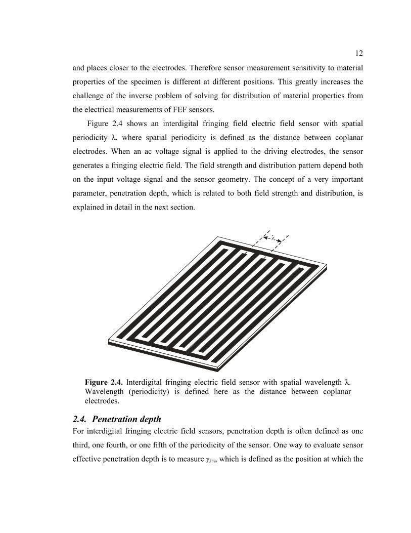
Figure 2.4 shows an interdigital fringing field electric field sensor with spatial
periodicity λ, where spatial periodicity is defined as the distance between coplanar
electrodes. When an ac voltage signal is applied to the driving electrodes, the sensor
generates a fringing electric field. The field strength and distribution pattern depend both
on the input voltage signal and the sensor geometry. The concept of a very important
parameter, penetration depth, which is related to both field strength and distribution, is
explained in detail in the next section.
Figure 2.4. Interdigital fringing electric field sensor with spatial wavelength λ. Wavelength (periodicity) is defined here as the distance between coplanar electrodes.
2.4. Penetration depth For interdigital fringing electric field sensors, penetration depth is often defined as one
third, one fourth, or one fifth of the periodicity of the sensor. One way to evaluate sensor
effective penetration depth is to measure γ3%, which is defined as the position at which the
13
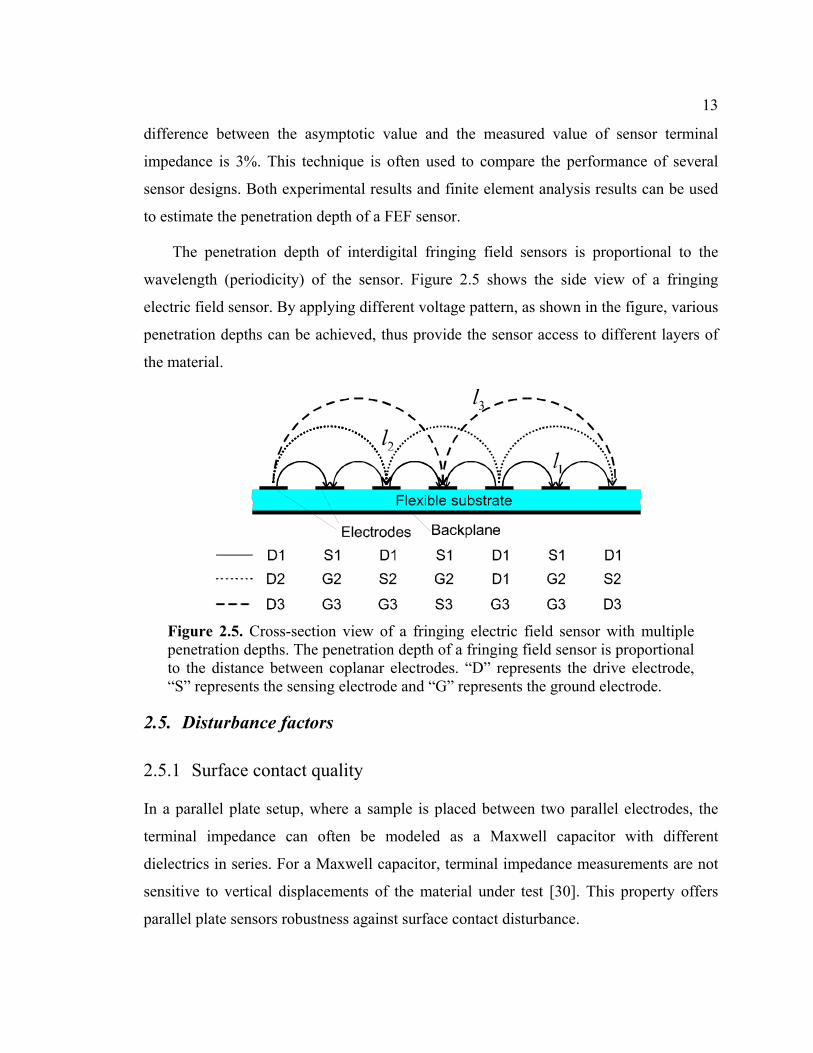
difference between the asymptotic value and the measured value of sensor terminal
impedance is 3%. This technique is often used to compare the performance of several
sensor designs. Both experimental results and finite element analysis results can be used
to estimate the penetration depth of a FEF sensor.
The penetration depth of interdigital fringing field sensors is proportional to the
wavelength (periodicity) of the sensor. Figure 2.5 shows the side view of a fringing
electric field sensor. By applying different voltage pattern, as shown in the figure, various
penetration depths can be achieved, thus provide the sensor access to different layers of
the material.
Figure 2.5. Cross-section view of a fringing electric field sensor with multiple penetration depths. The penetration depth of a fringing field sensor is proportional to the distance between coplanar electrodes. “D” represents the drive electrode, “S” represents the sensing electrode and “G” represents the ground electrode.
2.5. Disturbance factors
2.5.1 Surface contact quality
In a parallel plate setup, where a sample is placed between two parallel electrodes, the
terminal impedance can often be modeled as a Maxwell capacitor with different
dielectrics in series. For a Maxwell capacitor, terminal impedance measurements are not
sensitive to vertical displacements of the material under test [30]. This property offers
parallel plate sensors robustness against surface contact disturbance.

14
The scenario is quite different for FEF sensors. Since most of the field energy for
FEF sensors concentrates around electrodes, especially at the edges, the electrical
measurements from FEF sensors are very sensitive to uncertainties caused by surface
contact quality. This fact has to be considered when designing an experimental setup
involving FEF sensors. When the material under investigation is of liquid form, this issue
is not a problem. For solid samples, there are several ways to reduce this effect.
1. Since FEF sensors are capable of non-contact measurement, the sample can
be placed away from the sensor surface to a certain distance. Using air as an
intermediate dielectric, the effect of the surface irregularities of the electrode
and material surface will be attenuated. However, this method also reduces
the signal strength of the measurements.
2. Use flexible substrate and apply pressure from the top to ensure maximum
contact. Experimental results show that this method does reduce surface
disturbance to some extent, but not completely.
Due to the inherent strong non-linearity, it is difficult to find parameter estimation
algorithm that can compensate for the effect very well.
2.5.2 Stray capacitances
For the capacitive sensors used in this study, the magnitude of the electrical impedance
measurements is roughly proportional to the surface area of sensor electrodes. The
surface sensing area of fringing field sensors is usually less than that of their parallel
plate counter-parts. This results in a much weaker signal strength, which makes FEF
sensor measurements much more susceptible to noise.
Stray capacitance is a major source of disturbance. The capacitances between the
sensing electrodes and their respective back planes affect measurement accuracy if not
eliminated or compensated for.
Another source of stray capacitance is the sensor leads and the coaxial wires used to
connect the sensor with the interface circuit. These capacitances can be minimized by

15
proper shielding and reducing the length of the leads and the coaxial wires.
Operational amplifiers are usually used in the sensor interface circuit. The input
capacitance of op-amps is usually around 4 or 5 pF. The FEF sensor experimental
capacitance measurements involved in this study are usually at the scale of 0.01 to 0.1 pF.
This shows that, if not properly compensated for, the input impedance of the op-amps can
cause inaccuracy in the resulting measurements. Compensation is carried out here in this
thesis during circuit calibration. The exact procedures will be introduced in later chapters.
2.5.3 Deviation from ideal finite element analysis model
Finite element analysis simulations are often used to evaluate the performance of a sensor
and to the test the validity of experimental results. In the study of this thesis, the Ansoft
FEA software Maxell is used. Figure 2.6 shows the Maxwell simulation layout of the
interdigital sensor shown in Figure 2.4. For the simulation, several assumptions are made:
1. All fingers are of infinite length along the y direction.
2. The finger patterns are periodic along the x axis.
Deviations from this ideal model may lead to discrepancies between experimental and
Maxwell simulation results.
Figure 2.6. Maxwell simulation layout of a cookie sample positioned above an interdigital sensor. The wavelength of the sensor is 16 mm. It is assumed that the

16
fingers have infinite length and that the finger pattern is periodic along the horizontal axis.
2.5.4 Interfacial double layer effect
Figure 2.7 shows the circuit model for a test sample with double layer, where Cs and Rs
are the effective capacitance and resistance of the material under test while Cdl is the
double layer capacitance.
sZ
sCdlCdlC
sR
Figure 2.7. Illustration of the double layer effect. The double layer is formed at the metal-electrolyte boundaries [31]. Ions carrying
opposite charges are diffused into the other side of the boundary until equilibrium is
reached. The depth at which the diffusion process stops is called the Debye length. Debye
length is usually very small. This thin layer of opposite charges forms a great capacitance
Cdl.
The interfacial effect is more pronounced in case of liquid dielectrics, due to the
much higher tendency for diffusion. For example, a much stronger double layer effect is
observed for cookie dough samples than with ready-made cookies. The moisture and oil
in the cookie dough precipitate the diffusion process. One effective way of minimizing
the layer effect is to place a layer of polyimide film between the metal electrodes and the
sample under investigation. The polyamide film here serves as a liquid barrier. The water
absorption rate for polyamide is 3% of its dry weight. However, due to the high dielectric

17
permittivity of water, the dielectric property of the polyimide films changes a lot even
with minimal amount of moisture intake [7,32,33].
The DuPont Kapton is chosen as the barrier in this study. There are three common
varieties of Kapton films, Kapton HN, Kapton VN and Kapton FN, and they come in
different thicknesses ranging from 25 µm to 125 µm. Among all three, Kapton FN is most
hydrophobic, being coated on either or both sides with Teflon as an additional moisture
barrier.
The double layer capacitance causes inaccuracies in the estimates of the material
impedance Cs and Rs. Since the double layer capacitance is Cdl is usually much larger
than the effective material capacitance Cs, it dominates at low frequency. If the
operational frequency range is high enough, the interfacial effect can be ignored. The
measurements involved in this study are conducted at the frequency range of 50 Hz to
100 kHz, which is not high enough for the effect to be ignored.
It is easy to detect the double layer effect but difficult to estimate the exact value of
the Debye layer capacitance. One way to test the existence of the layer effect is by using
the Cole-Cole plot. The Cole-Cole plot of a capacitor and resistor in parallel is a semi-
circle. Deviation from a perfect semi-circle indicates the existence of the double layer.
The Debye length of the double layer can be estimated from the magnitude of the
deviation, yet to accurately quantify this effect is a non-trivial task. Therefore, the general
approach is to reduce, if not avoid, the double layer effect.

18
Chapter 3. Interdigital Fringing Field Dielectrometry
3.1. Overview of the measurement system Figure 3.1 shows the diagram of the measurement system used in the study of this thesis.
The central part of the system is the sensor array. The sensors designs have to be
optimized toward the particular application. An AC voltage signal comes from the signal
generator to the driving electrodes. The output signal from the sensing electrodes is
measured by the sensor interface circuit board. The electrical measurements then are sent
to the computer through an embedded data acquisition board. Labview software controls
the function generator through a GPIB board and also performs on-line data acquisition
and signal processing. The system works at the frequency range between 0.1 Hz to 30
kHz.
The work of the author focuses on the area of sensor design, sensor interface circuit
design, and Labview software development.
GPIB BOARD
COMPUTER
DAQ BOARD
SIGNAL GENERATOR
SENSORARRAY
SENSOR INTERFACE
POWER SUPPLY
Figure 3.1. Diagram of the measurement system.
Figure 3.2 shows the front panel of the Labview software user interface. The software allows real-time monitoring of impedance data in both the frequency and the time domain. For the particular application of cookie moisture sensing, the software can perform real-time moisture profile imaging of cookie dough samples.

19
Figure 3.2. Labview device control and data acquisition interface
Figure 3.3 shows the three channel interface circuit. The circuit is based on a voltage
divider scheme where the ratio of the magnitude of the output voltage signal and the
input voltage signal, and the phase delay between the input and the output are evaluated.
Unit gain buffers are used in the circuit to isolate the measured signal from the later
stages of the circuit. The circuit schematic is shown in Figure 3.4.

20
Figure 3.3. Three-channel sensor interface circuit.
Figure 3.4. Sensor interface circuit schematics.
3.2. Fringing electric field sensor design Parallel plate sensor designs are usually straightforward. The chapter focuses on the more
challenging task of designing FEF sensors, especially multi-channel FEF sensors.
However, some of the issues addressed here are common to all sensor designs.
3.2.1 Figures of merit
Sensor design is an optimization process, where several figures of merit have to be
considered simultaneously and necessary trade-offs are made. The major design goals are
explained in detail in this section.

21
3.2.1.1 Penetration depth The penetration depth of fringing field sensors is roughly proportional to the periodicity
of the sensor. The farther the electrodes are positioned away from each other, the higher
the penetration depth, which means the electrical field lines penetrate deeper into the test
specimen. For thick specimens, it is desirable to use sensors with large periodicity so that
sufficient penetration depth is accommodated.
3.2.1.2 Signal strength The design parameters that mostly determine the signal strength of a sensor are the total
sensor surface area and the relative metallization ratio. The greater these two parameters,
the stronger the signal strength. Metallization ratio is defined as the ratio of surface area
of the active electrodes (guard electrodes not included) against the total sensing area.
Most of the designs developed in this study use a 50% metallization ratio. Another
parameter that affects the signal strength is the magnitude of the input driving signal.
However, increasing the input also raises the noise floor. Thus, raising the input voltage
usually has little effect on the SNR, the major parameter of interest. A more efficient way
to improve SNR is to magnify the signal using instrumental amplifiers. The earlier the
amplification, but better the overall SNR performance.
3.2.1.3 Sensitivity Sensitivity is defined as the slope of the measurement curve, namely the ratio between
the measurement variation and the variation of the measured physical property. Due to
the uneven field distribution of FEF sensors, its measurement sensitivity varies at
different locations. As indicated by Figure 3.5, sensitivity decreases exponentially with
increasing distance between the specimen and the sensor. Thus, to maximize sensitivity,
it is desirable to position the specimen as close to the sensor as possible. This is
especially important when considering that signal strength of FEF sensors is usually
weak.
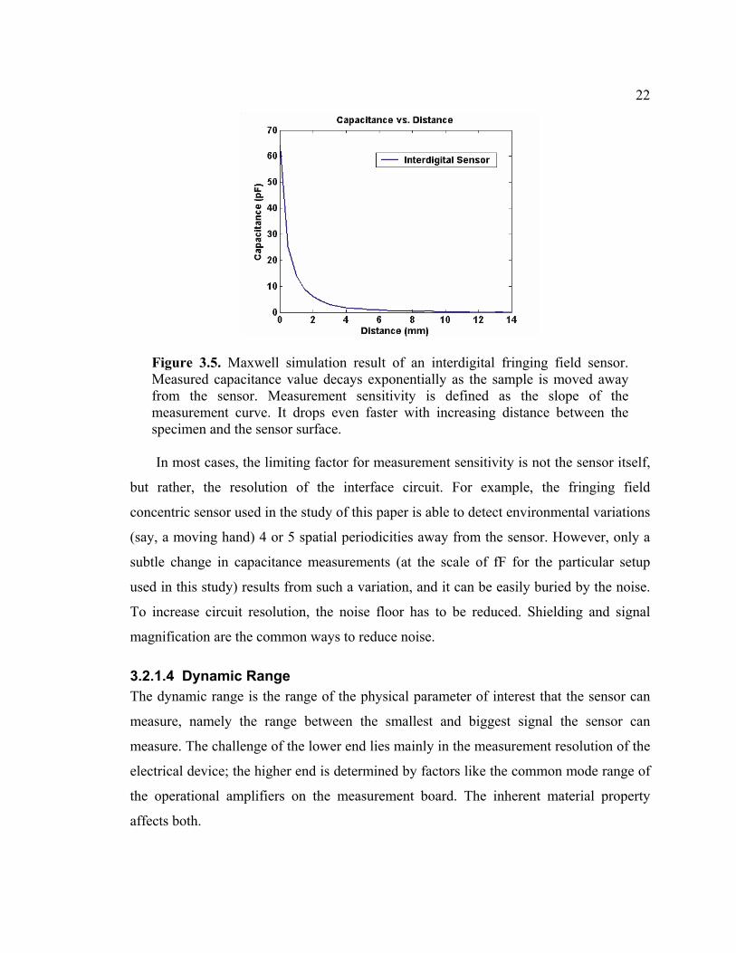
22
Figure 3.5. Maxwell simulation result of an interdigital fringing field sensor. Measured capacitance value decays exponentially as the sample is moved away from the sensor. Measurement sensitivity is defined as the slope of the measurement curve. It drops even faster with increasing distance between the specimen and the sensor surface. In most cases, the limiting factor for measurement sensitivity is not the sensor itself,
but rather, the resolution of the interface circuit. For example, the fringing field
concentric sensor used in the study of this paper is able to detect environmental variations
(say, a moving hand) 4 or 5 spatial periodicities away from the sensor. However, only a
subtle change in capacitance measurements (at the scale of fF for the particular setup
used in this study) results from such a variation, and it can be easily buried by the noise.
To increase circuit resolution, the noise floor has to be reduced. Shielding and signal
magnification are the common ways to reduce noise.
3.2.1.4 Dynamic Range The dynamic range is the range of the physical parameter of interest that the sensor can
measure, namely the range between the smallest and biggest signal the sensor can
measure. The challenge of the lower end lies mainly in the measurement resolution of the
electrical device; the higher end is determined by factors like the common mode range of
the operational amplifiers on the measurement board. The inherent material property
affects both.

23
3.2.1.5 Number of channels Sometimes, instead of using sensor arrays, it is desirable to fit multiple channels on the
same sensor. The more channels the sensor has, the more information available about the
material.
3.2.1.6 Noise tolerance Guard planes are usually introduced to improve sensor noise performance. This includes
both the guard ring on the top plane of the sensor surface and the guard plane at the back
of the sensor substrate. Proper positioning of these guard electrodes is essential for
optimal results. In addition, it is desirable to have all the driving electrodes on both sides
of all sensing electrodes. However, this might be difficult to accommodate in some cases
due to size limitation.
3.2.2 Major design concerns
3.2.2.1 Choice of sensor substrate
The choice of sensor substrate should be optimized toward the particular application.
Major points to consider are:
1. Should the substrate flexible or rigid?
2. What are the desired electrical, mechanical, and chemical properties for the sensor
substrate of this particular application? For example, does it matter whether the
material is hydrophilic or hydrophobic? This is of particular importance due to the
double layer effect that often occurs in dielectrometry measurements.
Proper choices should be made based on the answer to these questions. For certain
application, no substrate is necessary. The electrode can be applied directly to the test
specimen.
3.2.2.2 Choice of electrode material
3.2.2.2.1 Surface contact quality
For applications with solid dielectrics, surface contact quality is one of the major sources
of measurement uncertainties. Any air gap between the electrodes and the test specimen
24
acts as a capacitance in series with the RC component of the specimen and results in a
decreased measurement in both the material capacitance and conductance. For accurate
measurements, the test specimen should be measured by thin metallic electrodes before
put between rigid electrodes. Such products as silver paints and low-melting metals that
can be applied with a spray-gun are commercially available. They conform readily to the
surface of rough specimens and can greatly improve surface contact quality. The
disadvantages of these electrodes are that they are usually difficult to pattern and remove
[34].
In clinical applications of electrical impedance tomography, saline gels are utilized
to improve electrode and skin contact. The most widely used is NaCl gel. The
concentration of NaCl has to be carefully controlled to avoid irritating the skin. Aside
from improved contact quality, the electrolyte also helps to reduce the contact impedance
by hydrating the skin [35].
3.2.2.2.2 Novel electrode materials
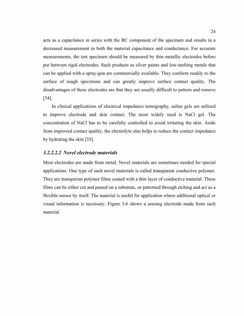
Most electrodes are made from metal. Novel materials are sometimes needed for special
applications. One type of such novel materials is called transparent conductive polymer.
They are transparent polymer films coated with a thin layer of conductive material. These
films can be either cut and pasted on a substrate, or patterned through etching and act as a
flexible sensor by itself. The material is useful for application where additional optical or
visual information is necessary. Figure 3.6 shows a sensing electrode made from such
material.

25
Figure 3.6. Transparent sensor fabricated by sputtering Indium Tin Oxide onto a thin polyester sheet.
3.2.2.3 Size limitation If the sensor is embedded on a flexible substrate, the sensor can be wrapped around the
test specimen to guarantee that all parts of the material are sensed. For sensor with rigid
substrate, however, the size of the fringing field sensor is usually limited by the size of
the material under investigation. Usually, the sensor should be of the same size or smaller
than the material so that all the surface area of the sensor is covered by the material. For
small and thick specimens, it is usually hard to design a sensor that has sufficient
penetration depth due to the electrode surface area limit posed by the size of the material.
3.2.2.4 Trade off between penetration depth, signal strength and the number of channels
Due to the sensor electrode surface area limitation mentioned above, there is a trade-off
between the penetration depth of the sensor and the number of channels that can be fit on
the sensor. To fit more channels on the sensor, the sensor electrodes have to be squeezed
closer together, the penetration depth, in turn, is affected. Equally harmed is the signal
strength of the sensor due to the reduced electrode surface area for each channel.
3.2.2.5 Cross talk between channels The closer the channels are positioned together, the stronger the cross talk between the
channels. It is desirable to position the channels a far apart as possible. In this way, cross

26
talk reduction is obtained by sacrificing sensor surface area and this comes with the price
of loss in signal strength and penetration depth. One solution to this problem is by
grounding the sensing electrodes of the channels not being used. However, this method
increases the complexity of the interface circuit, and only works when simultaneous
measurements are not required.
3.2.2.6 The positioning and the geometry of the back plane The back plane and the top sensor electrodes are separated by the substrate. Most sensor
substrates are very thin compared with the periodicity of the sensor. Due to the close
proximity of the sensor back plane to the top electrodes, the distribution of the sensor
field patterns is very sensitive to the positioning and the geometry of the back plane. The
field lines and field energy tend to be drawn away from the material being sensed by the
back plane, therefore, affecting the penetration depth and signal strength. Proper
positioning of the sensor back plane is thus essential to optimize sensor performance.
This is achieved mostly from design experience and with the help of Maxwell
simulations. Aside from these factors, attention should also be taken about the voltage
potential of the back planes. Whether they are grounded or set to the same voltage as the
top sensing electrodes also makes a difference in the resulting field energy distribution.
3.2.2.7 The thickness of the substrate As mentioned above, the thickness of FEF sensor substrate determines the distance
between the back planes to the top electrodes, which in turn affects the distribution of
field energy. To further illustrate this idea, Maxwell simulations are carried out, where a
concentric-ring fringing field sensor setup is simulated and the thickness of the substrate
varied from 97% to 25% of its original value. A test sample is moved away from the
sensor surface in this setup. The simulation results are shown in Figure 3.7. Capacitance
measurements are shown to decrease with decreasing substrate thickness. The thinner the
sensor substrate, the closer the back plane to the top electrodes and the more energy is
drawn away for the test specimen.

27
0 2 4 6 8 100
0.2
0.4
0.6
0.8
1
1.2
1.4
1.6
Distance (mm)
Cap
acita
nce
(pF)
97%50%25%
Figure 3.7. Maxwell simulation results of a concentric-ring fringing field setup. The substrate thickness is varied from 97% to 25% of its original value.
3.2.2.8 Conclusion The major obstacle in fringing field sensor design is the size limitation posed by the
geometry of the test specimen. The design goal is to fit as many channels as possible on
the sensor while still accommodating sufficient penetration depth and signal strength.
Novel sensor design and excitation patterns are being investigated to achieve this goal.
Other factors such as substrate thickness and back plane geometry should also be
considered.
3.2.3 Example of multi-channel fringing field sensor designs
3.2.3.1 Interdigital FEF sensors Figure 3.8 and Figure 3.9 show two different designs of multi-channel sensors. The one
shown in Figure 3.8 has three channels, each providing a different penetration depth.
Thus, the sensor has access to different layers of the test specimen and can provide
information on the specimen at these different layers. This is, however, only true for
homogeneous materials. In the case of an inhomogeneous specimen, it is difficult to
conduct comparative analysis on the measurements from the three different channels.
This is because the spatial information along the depth of the material and the horizontal

28
surface of the material are coupled together and extracting the depth information is a non-
trivial task.
Figure 3.8. Three-wavelength fringing electric field sensor.
Figure 3.9 shows an improved design. It still offers three measurement channels. In
addition, all three channels measure the specimen at the same horizontal location. In this
way, information on the distribution of material property at different layers can be
obtained by comparing the measurements from different channels.

29
Figure 3.9. Three-wavelength fringing electric field sensor.
3.2.3.2 Concentric FEF sensors
It is often necessary to optimize sensor geometry towards the geometry of the test
specimen. Figure 3.10 shows a concentric sensor head designed for measuring moisture
content in cookie dough samples, which usually assume a near-symmetric rounds shape.
The sensor can act as a two-channel FEF sensor, by using the center electrode as the
driving electrode and the other two electrodes as the sensing electrodes. The two sensing
channels of this sensor have roughly the same penetration depth due to the similarity in
wavelength/periodicity. The sensor measures the material at two different radial
locations. Vertical information about the test specimen at different layers can be obtained
by varying the distance between the sensor surface and the specimen.
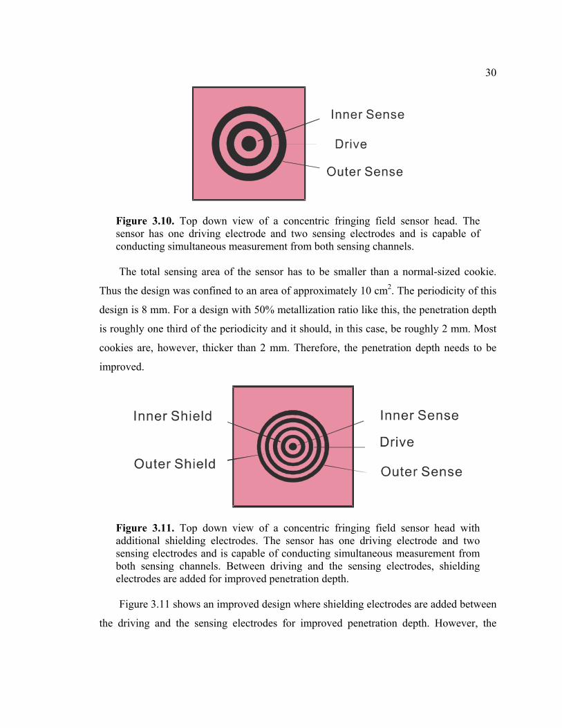
30
Figure 3.10. Top down view of a concentric fringing field sensor head. The sensor has one driving electrode and two sensing electrodes and is capable of conducting simultaneous measurement from both sensing channels. The total sensing area of the sensor has to be smaller than a normal-sized cookie.
Thus the design was confined to an area of approximately 10 cm2. The periodicity of this
design is 8 mm. For a design with 50% metallization ratio like this, the penetration depth
is roughly one third of the periodicity and it should, in this case, be roughly 2 mm. Most
cookies are, however, thicker than 2 mm. Therefore, the penetration depth needs to be
improved.
Figure 3.11. Top down view of a concentric fringing field sensor head with additional shielding electrodes. The sensor has one driving electrode and two sensing electrodes and is capable of conducting simultaneous measurement from both sensing channels. Between driving and the sensing electrodes, shielding electrodes are added for improved penetration depth. Figure 3.11 shows an improved design where shielding electrodes are added between
the driving and the sensing electrodes for improved penetration depth. However, the

31
surface area of the active electrodes is sacrificed and the overall signal strength is
reduced.
3.2.3.3 Evaluation of sensor penetration depth Maxwell simulation allows us to evaluate the performance of a particular design before
the sensor is fabricated. Penetration depth is one of the major parameters of interest.
Figure 3.12 shows the layout of the Maxwell simulation for the concentric fringing field
sensor without shielding electrodes. In this simulation, the cookie sample is assumed to
have a real dielectric permittivity of 5.0. Penetration depth γ3% is defined here as the
distance at which measured capacitance drops to 3% of its asymptotic value (at infinite
distance).
Figure 3.12. Maxwell simulation layout of a cookie sample positioned above the concentric fringing field sensor. The simulation is carried out using the RZ radial coordinates. The capacitance data is normalized to a range between 0 and 100%. Penetration
depth can be estimated from the distance corresponding to the intersection point between
the normalized measurement curve and the 3% line. Figure 3.13 and Figure 3.14 show
respectively the normalized capacitance data from the inner and outer channel of the first
concentric sensor design.
It is worthy to note that is that instead of dropping monotonically with increasing
distance, the capacitance measurement from the inner channel actually goes up a bit at

32
the distance from 6 to 10 mm. To explain this phenomenon, the field line distribution
dynamics has to be considered. When the specimen is within certain distance to the
sensor surface, the relative high dielectric permittivity of the specimen draws the electric
field energy towards itself, thus alters the field line distribution. This change in field
distribution is the major reason for the rise in the capacitance measurement.
Figure 3.13. Normalized capacitance measurement from the inner sensing channel of the first concentric sensor design. The measured capacitance doesn’t change monotonically with distance.
Figure 3.14. Normalized capacitance measurement from the outer sensing channel of the first concentric sensor design. A monotonic dependence exists between capacitance measurement and the distance.
3.2.3.4 Comparative performance analysis of the two concentric designs The motivation behind adding the shielding electrodes in the second concentric fringing
sensor design is to improve sensor penetration depth, as illustrated in Figure 3.15.

33
Figure 3.15. The addition of shielding electrodes in the fringing electric sensor increases penetration depth.
Maxwell simulations are conducted to evaluate the effectiveness of this approach. Figure
3.16 and Figure 3.17 show respectively the absolute and normalized capacitance
measurement from the inner and outer channels on both sensors. Sensor 1 refers to the
design without shielding electrodes and sensor 2 refers to the one with shielding
electrodes. For both designs, the outer channel offer better signal strength and penetration
depth. The difference in signal strength is caused by the relative larger sensing area of the
outer channel. When comparing the performance between the two sensor designs, the
second design provides greater penetration depth at the price of decreased signal strength.
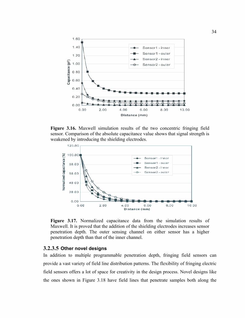
34
Figure 3.16. Maxwell simulation results of the two concentric fringing field sensor. Comparison of the absolute capacitance value shows that signal strength is weakened by introducing the shielding electrodes.
Figure 3.17. Normalized capacitance data from the simulation results of Maxwell. It is proved that the addition of the shielding electrodes increases sensor penetration depth. The outer sensing channel on either sensor has a higher penetration depth than that of the inner channel.
3.2.3.5 Other novel designs In addition to multiple programmable penetration depth, fringing field sensors can
provide a vast variety of field line distribution patterns. The flexibility of fringing electric
field sensors offers a lot of space for creativity in the design process. Novel designs like
the ones shown in Figure 3.18 have field lines that penetrate samples both along the
35
radial axis and tangential to the radial axis. The field patterns can be optimized toward a
particular application through proper arrangement of the electrodes. However, these two
designs are not as space efficient as the concentric design. Thus they are not used in the
current application.
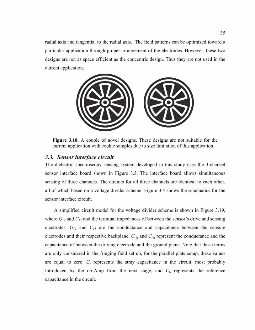
Figure 3.18. A couple of novel designs. These designs are not suitable for the current application with cookie samples due to size limitation of this application.
3.3. Sensor interface circuit The dielectric spectroscopy sensing system developed in this study uses the 3-chaneel
sensor interface board shown in Figure 3.3. The interface board allows simultaneous
sensing of three channels. The circuits for all three channels are identical to each other,
all of which based on a voltage divider scheme. Figure 3.4 shows the schematics for the
sensor interface circuit.
A simplified circuit model for the voltage divider scheme is shown in Figure 3.19,
where G12 and C12 and the terminal impedances of between the sensor’s drive and sensing
electrodes. G11 and C11 are the conductance and capacitance between the sensing
electrodes and their respective backplane. Gdg and Cdg represent the conductance and the
capacitance of between the driving electrode and the ground plane. Note that these terms
are only considered in the fringing field set up, for the parallel plate setup, these values
are equal to zero. Cs represents the stray capacitance in the circuit, most probably
introduced by the op-Amp from the next stage, and CL represents the reference
capacitance in the circuit.

36
Since Gdg and Cdg are connected directly to the voltage input, they have no effect on
the output voltage measurement. Therefore, they can be ignored in the circuit analysis.
G11 and C11, however, affect the output voltage Vs and they are unknown and difficult to
estimate.
To eliminate the effects of G11 and C11, the circuit was modified to the one shown in
Figure 3.20. In this connection scheme, the back plane for each electrode is set to the
same voltage potential as their respective sensing electrode through a unity gain buffer
operational amplifier, which removes the effects of G11 and C11.
Figure 3.19. Floating voltage with ground.
Figure 3.20. Floating voltage with guard.

37
38
Chapter 4. Moisture dynamics in cookies
4.1. Definition of the problem Lack of process control has been thwarting food manufacturer’s efforts to reduce
production cost. Moisture content is one of the major control parameters of concern.
Accurate control of moisture content is critical to achieving the right taste and texture for
food products. By incorporating a moisture sensor in the feedback loop of the
manufacturing process, the moisture content can be accurately controlled in real time.
The integration of advanced sensing technologies in the cookie manufacturing process
allows automatic production of complex cookies that has been possible so far only in
bakeries. In this investigation, moisture content is determined from the impedance
measurements of the material of interest. Moisture concentration is defined here as
follows:
1%
1 2100%MM
M M= ×
+ (4.1)
where M1 is the mass of the moisture contained in the unit volume, and M2 is the mass of
the dry portion of the material in the same unit volume.
Material impedance is a function of many variables, as shown in (4.2), where M% is
the moisture concentration in the material, T is the ambient temperature, D is the sample
density, and ω is the input signal frequency.
%( , , , )s ZZ f M T D ω= (4.2)
System calibration involves solving the inverse problem of determining the
following function:
% ( , , , )M sM f Z T D ω= (4.3)
or
% ( )M sM f Z= (4.4)
where the functional dependence between moisture concentration and the impedance is to
be determined. The effects from variables other than moisture content are either
eliminated or accounted for.
39
4.2. Methodology The material contents of food products are usually complex and varying, which renders
direct determination of sample dielectric permittivity difficult and impractical. Under
these circumstances, an indirect parameter estimation approach based on quantitative
mapping between electrical measurements and the physical variable of interest can be
used. The major challenge for such an approach lies in minimizing the effect of variables
other than moisture concentration, such as ambient temperature and sample density,
which are considered here as disturbance factors. The effects of these factors should
either be eliminated or accounted for in the calibration algorithm [36].
4.3. Experimental setup
4.3.1 The Concentric Sensor Head
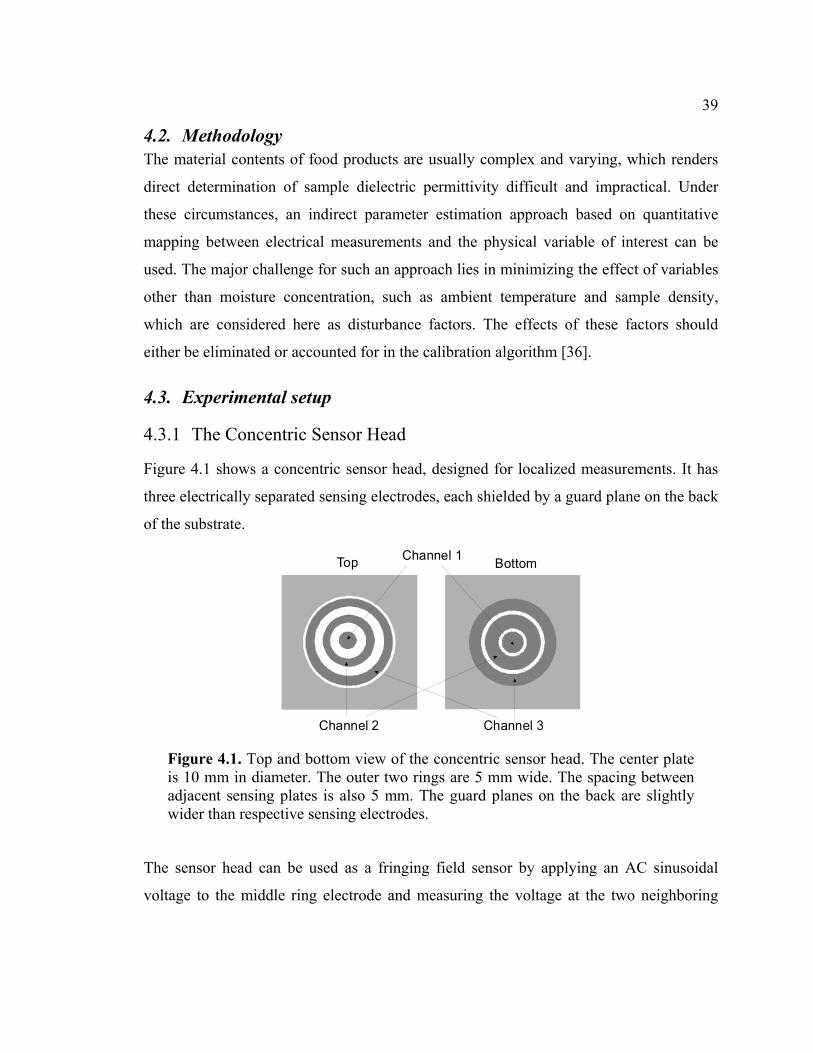
Figure 4.1 shows a concentric sensor head, designed for localized measurements. It has
three electrically separated sensing electrodes, each shielded by a guard plane on the back
of the substrate.
Channel 1 BottomTop
Channel 3Channel 2
Figure 4.1. Top and bottom view of the concentric sensor head. The center plate is 10 mm in diameter. The outer two rings are 5 mm wide. The spacing between adjacent sensing plates is also 5 mm. The guard planes on the back are slightly wider than respective sensing electrodes.
The sensor head can be used as a fringing field sensor by applying an AC sinusoidal
voltage to the middle ring electrode and measuring the voltage at the two neighboring
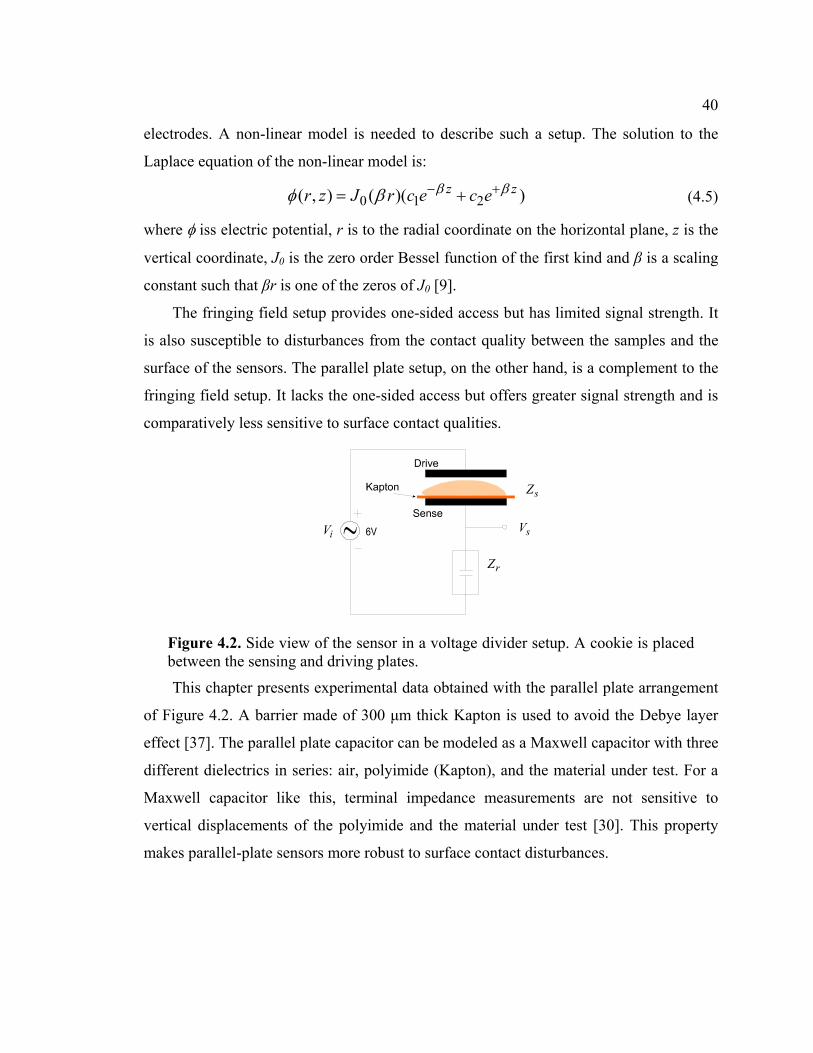
40
electrodes. A non-linear model is needed to describe such a setup. The solution to the
Laplace equation of the non-linear model is:
0 1 2( , ) ( )( )z zr z J r c e c eβ βφ β − += + (4.5)
where φ iss electric potential, r is to the radial coordinate on the horizontal plane, z is the
vertical coordinate, J0 is the zero order Bessel function of the first kind and β is a scaling
constant such that βr is one of the zeros of J0 [9].
The fringing field setup provides one-sided access but has limited signal strength. It
is also susceptible to disturbances from the contact quality between the samples and the
surface of the sensors. The parallel plate setup, on the other hand, is a complement to the
fringing field setup. It lacks the one-sided access but offers greater signal strength and is
comparatively less sensitive to surface contact qualities.
Figure 4.2. Side view of the sensor in a voltage divider setup. A cookie is placed between the sensing and driving plates.
This chapter presents experimental data obtained with the parallel plate arrangement
of Figure 4.2. A barrier made of 300 µm thick Kapton is used to avoid the Debye layer
effect [37]. The parallel plate capacitor can be modeled as a Maxwell capacitor with three
different dielectrics in series: air, polyimide (Kapton), and the material under test. For a
Maxwell capacitor like this, terminal impedance measurements are not sensitive to
vertical displacements of the polyimide and the material under test [30]. This property
makes parallel-plate sensors more robust to surface contact disturbances.

41
4.3.2 A Voltage Divider Circuit
Figure 4.2 shows a voltage divider circuit, where Vi is the input voltage signal, Vs is the
sensing voltage signal, Zr is the reference impedance, and Zs is the sensing impedance.
The effective impedance of the parallel-plate capacitor is calculated from the voltage
divider relationship 4.6. To maximize circuit sensitivity, Zr is chosen to be close to Zs. In
this investigation, Zr = 8 pF.
s r
i r s
V ZV Z Z
=+
(4.6)
Various connection schemes are available for this voltage divider setup [38]. When
there is an electric potential difference between the sensing electrodes and their
respective guard electrodes, stray capacitances are introduced into the circuit. To prevent
these stray capacitances from affecting measurement accuracy, the guard planes are set to
the same voltage as their respective sensing electrodes by using a unity-gain voltage
buffer.
Figure 4.3. Detailed circuit model considering double layer effect.
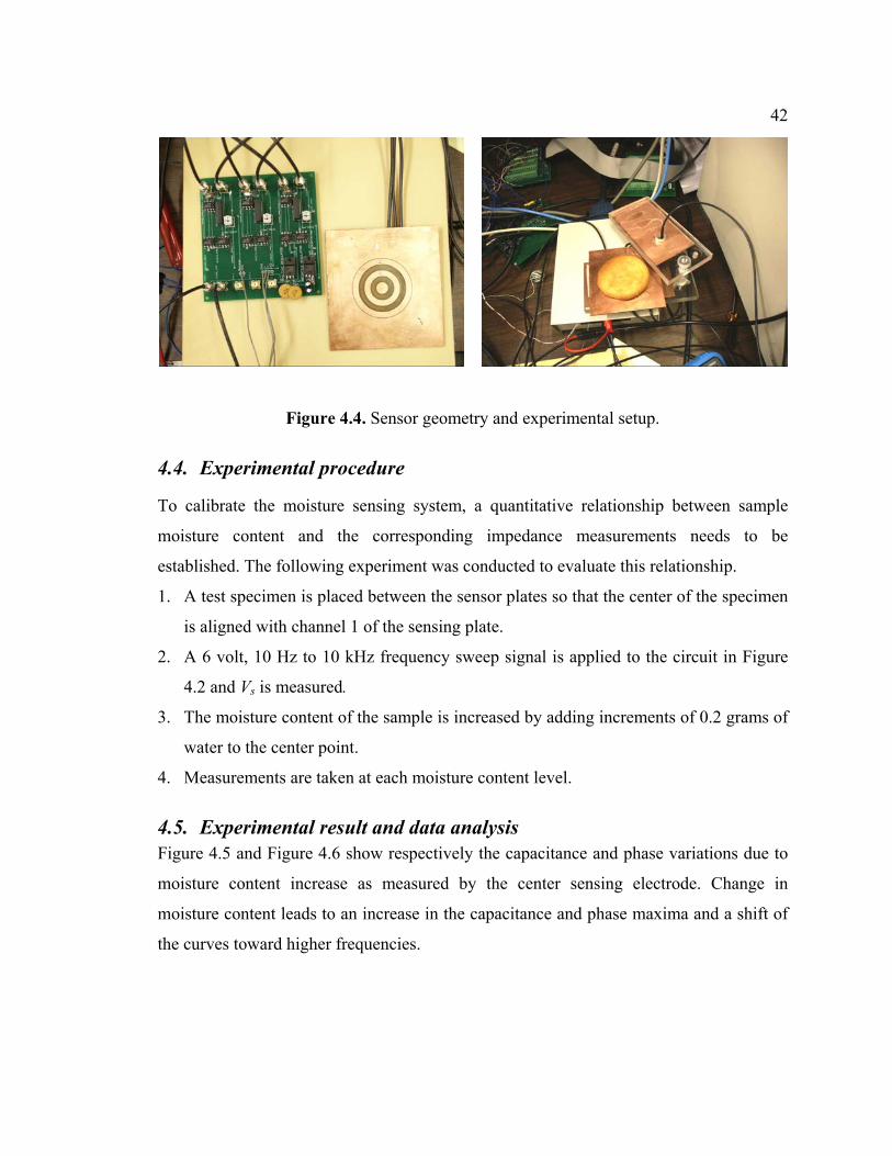
42
Figure 4.4. Sensor geometry and experimental setup.
4.4. Experimental procedure
To calibrate the moisture sensing system, a quantitative relationship between sample
moisture content and the corresponding impedance measurements needs to be
established. The following experiment was conducted to evaluate this relationship.
1. A test specimen is placed between the sensor plates so that the center of the specimen
is aligned with channel 1 of the sensing plate.
2. A 6 volt, 10 Hz to 10 kHz frequency sweep signal is applied to the circuit in Figure
4.2 and Vs is measured.
3. The moisture content of the sample is increased by adding increments of 0.2 grams of
water to the center point.
4. Measurements are taken at each moisture content level.
4.5. Experimental result and data analysis Figure 4.5 and Figure 4.6 show respectively the capacitance and phase variations due to
moisture content increase as measured by the center sensing electrode. Change in
moisture content leads to an increase in the capacitance and phase maxima and a shift of
the curves toward higher frequencies.
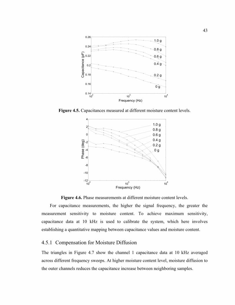
43
102
103
1040.14
0.16
0.18
0.2
0.22
0.24
0.26
Cap
acita
nce
(pF)
Frequency (Hz)
0 g
1.0 g
0.8 g
0.6 g
0.4 g
0.2 g
Figure 4.5. Capacitances measured at different moisture content levels.
102
103
104-12
-10
-8
-6
-4
-2
0
2
4
Frequency (Hz)
Pha
se (d
eg)
0 g
1.0 g0.8 g0.6 g0.4 g0.2 g
Figure 4.6. Phase measurements at different moisture content levels.
For capacitance measurements, the higher the signal frequency, the greater the
measurement sensitivity to moisture content. To achieve maximum sensitivity,
capacitance data at 10 kHz is used to calibrate the system, which here involves
establishing a quantitative mapping between capacitance values and moisture content.
4.5.1 Compensation for Moisture Diffusion
The triangles in Figure 4.7 show the channel 1 capacitance data at 10 kHz averaged
across different frequency sweeps. At higher moisture content level, moisture diffusion to
the outer channels reduces the capacitance increase between neighboring samples.

44
The higher the moisture content gradient between the center channel and the outer
rings, the more intensive the moisture diffusion process. This is reflected in the
increasing discrepancy between the uncompensated and compensated capacitance data as
water is being added to the center of the sample.
0.2 0.4 0.6 0.8 1 1.20
0.02
0.04
0.06
0.08
0.1
0.12
0.14
0.16
0.18
0.2
Moisture (g)
Cap
acita
nce
(pF)
Before compensation
After compensation
*16.4390 0.0028M C∆ = × ∆ +
Figure 4.7. Capacitance measurements against the mass of added water at 10 kHz for channel 1. Saturation occurs at high water level.
To compensate for the effect of diffusion, the capacitance increase from channels 2
and 3 is measured and mapped to effective increase in channel 1. This increase, added to
the original capacitance change from channel 1, gives the new channel 1 capacitance data
after compensation, as shown in (4.7), where ∆C is the capacitance increase for each
channel, Cor is the capacitance measurement of the original sample for each channel, and
∆C1* is the channel 1 capacitance increase after compensation.
* 1 11 1 2 3
2 3
or or
or or
C CC C C CC C
∆ = ∆ + ∆ + ∆ (4.7)
As indicated by the solid line in Figure 4.7, a much better linear approximation is
achieved after compensation.
4.5.2 Linear Regression
Assuming a linear functional dependence, the following calibration equation is
determined for channel 1 by performing linear regression on the compensated data:

45
31 16.44 2.8 10M C −∆ = × ∆ + × (4.8)
In this configuration, all sensor pixels are parallel-plate capacitors with different area.
Ideally, the functional dependence for channels 2 and 3 can be obtained by scaling (4.8)
with the respective area ratio. However, the existence of a non-uniform air gap has to be
taken into account.
4.5.3 Compensation for Non-Uniform Air Gap
The air gap between the material and the top plate of the sensor is non-uniform due to an
uneven shape of the cookie samples. To compensate for this, uniform water distribution
in the original sample is assumed and the ratios of capacitance measurements from
channels 2 and channel 3 with respect to channel 1 are measured. This difference in
capacitance measurements from the three channels is caused partly by the difference in
sensing plate area and partly by the non-uniformity in air gap thickness. Taking the ratios
obtained above and using them as scaling factors, the functional dependence of
capacitance measurements on water content from channels 2 and 3 can be obtained from
(4.8).
4
2 21.43 6.22 10M C −∆ = × ∆ + × (4.9)
4
3 30.91 3.95 10M C −∆ = × ∆ + × (4.10)
4.5.4 Moisture Content Distribution
Based on the calibration equations (4.8), (4.9), and (4.10), the absolute mass of moisture
contained in the portion of the sample above each ring is calculated from the capacitance
measurements. The mass of the dry portion of the sample above each ring is determined
from the ratio of the respective sensing electrode area to the area of the whole sample.
Given the absolute mass of moisture and the dry portion of the sample, moisture content
levels for all three channels can be calculated according to (4.1), enabling real-time
imaging of moisture content distribution.
Figure 4.8 shows the moisture content distribution profile of a sample at various
moisture content levels, which is obtained from fitting the moisture content data from the
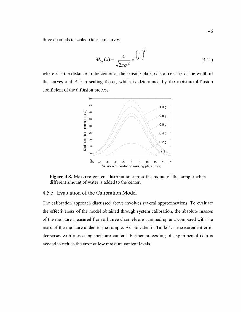
46
three channels to scaled Gaussian curves.
2
% 2( )
2
xAM x e σ
πσ
− = (4.11)
where x is the distance to the center of the sensing plate, σ is a measure of the width of
the curves and A is a scaling factor, which is determined by the moisture diffusion
coefficient of the diffusion process.
Figure 4.8. Moisture content distribution across the radius of the sample when different amount of water is added to the center.
4.5.5 Evaluation of the Calibration Model
The calibration approach discussed above involves several approximations. To evaluate
the effectiveness of the model obtained through system calibration, the absolute masses
of the moisture measured from all three channels are summed up and compared with the
mass of the moisture added to the sample. As indicated in Table 4.1, measurement error
decreases with increasing moisture content. Further processing of experimental data is
needed to reduce the error at low moisture content levels.
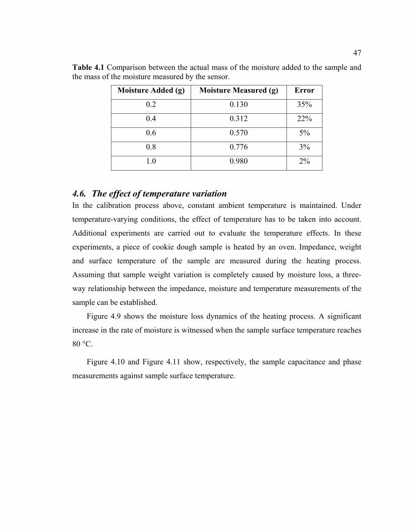
47
Table 4.1 Comparison between the actual mass of the moisture added to the sample and the mass of the moisture measured by the sensor.
Moisture Added (g) Moisture Measured (g) Error
0.2 0.130 35%
0.4 0.312 22%
0.6 0.570 5%
0.8 0.776 3%
1.0 0.980 2%
4.6. The effect of temperature variation In the calibration process above, constant ambient temperature is maintained. Under
temperature-varying conditions, the effect of temperature has to be taken into account.
Additional experiments are carried out to evaluate the temperature effects. In these
experiments, a piece of cookie dough sample is heated by an oven. Impedance, weight
and surface temperature of the sample are measured during the heating process.
Assuming that sample weight variation is completely caused by moisture loss, a three-
way relationship between the impedance, moisture and temperature measurements of the
sample can be established.
Figure 4.9 shows the moisture loss dynamics of the heating process. A significant
increase in the rate of moisture is witnessed when the sample surface temperature reaches
80 °C.
Figure 4.10 and Figure 4.11 show, respectively, the sample capacitance and phase
measurements against sample surface temperature.
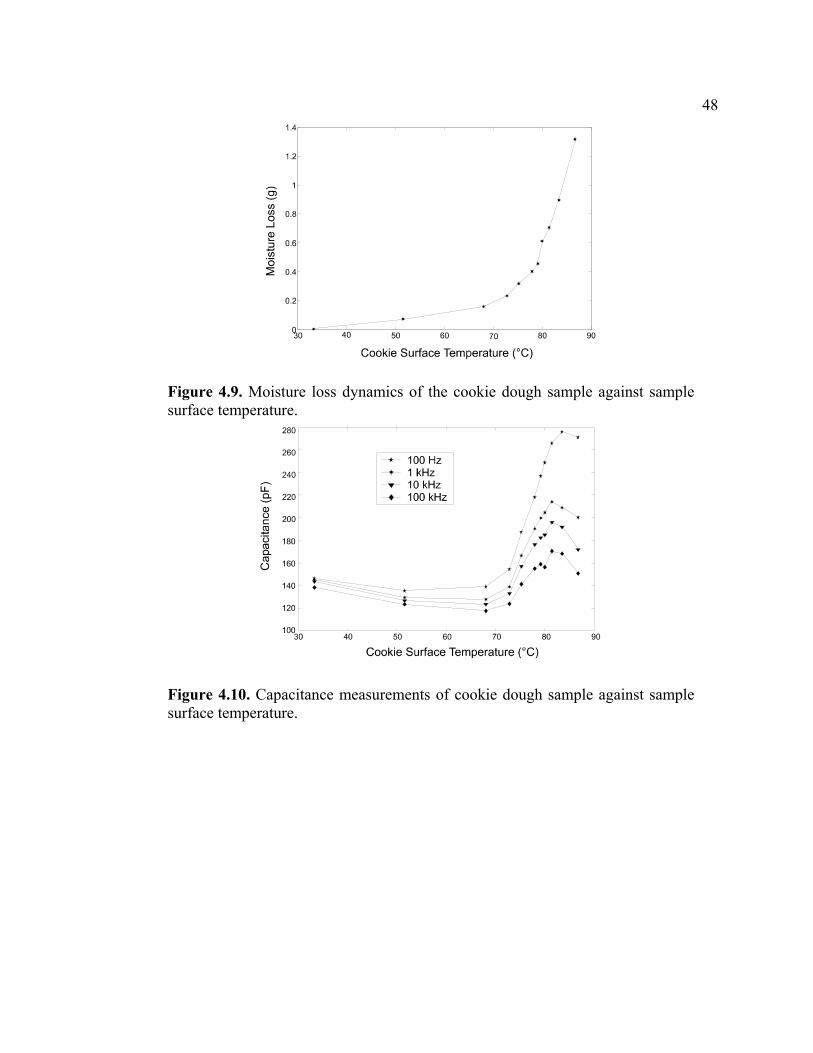
48
Figure 4.9. Moisture loss dynamics of the cookie dough sample against sample surface temperature.
Figure 4.10. Capacitance measurements of cookie dough sample against sample surface temperature.

49
Figure 4.11. Phase measurements of cookie dough sample against sample surface temperature.
4.6.1 The double layer effect
Double layer is formed at the interface between metal and electrolytes. At the metal-
dielectrics boundary, the ions carrying opposite charges diffused into the other side of the
boundary. This thin layer of charges forms a very big capacitance in series with the
capacitance and conductance of the dielectric material under consideration.
The cookie dough has much higher moisture content than the cookies used in the
previous constant temperature experiments. Therefore, the double layer effect which is
almost negligible in the previous case is now much more pronounced. The adoption of a
layer of polyimide between the material and sensor electrode surface still can not
completely eliminate the effect.
4.6.2 Lumped circuit simulation
To confirm the existence of the double layer effect, simulation of a lumped circuit model
as shown in Figure 4.12 was carried out, where C1 and R1 represent the capacitance and
resistance of the test sample and C2 represents the capacitance due to double layer effect.
The exact value of C2 is difficult to estimate. The existence of the unknown capacitance
makes it much more challenging to measure sample impedance accurately. Therefore,
double layer effect is undesirable. Kapton was used in the previous constant temperature
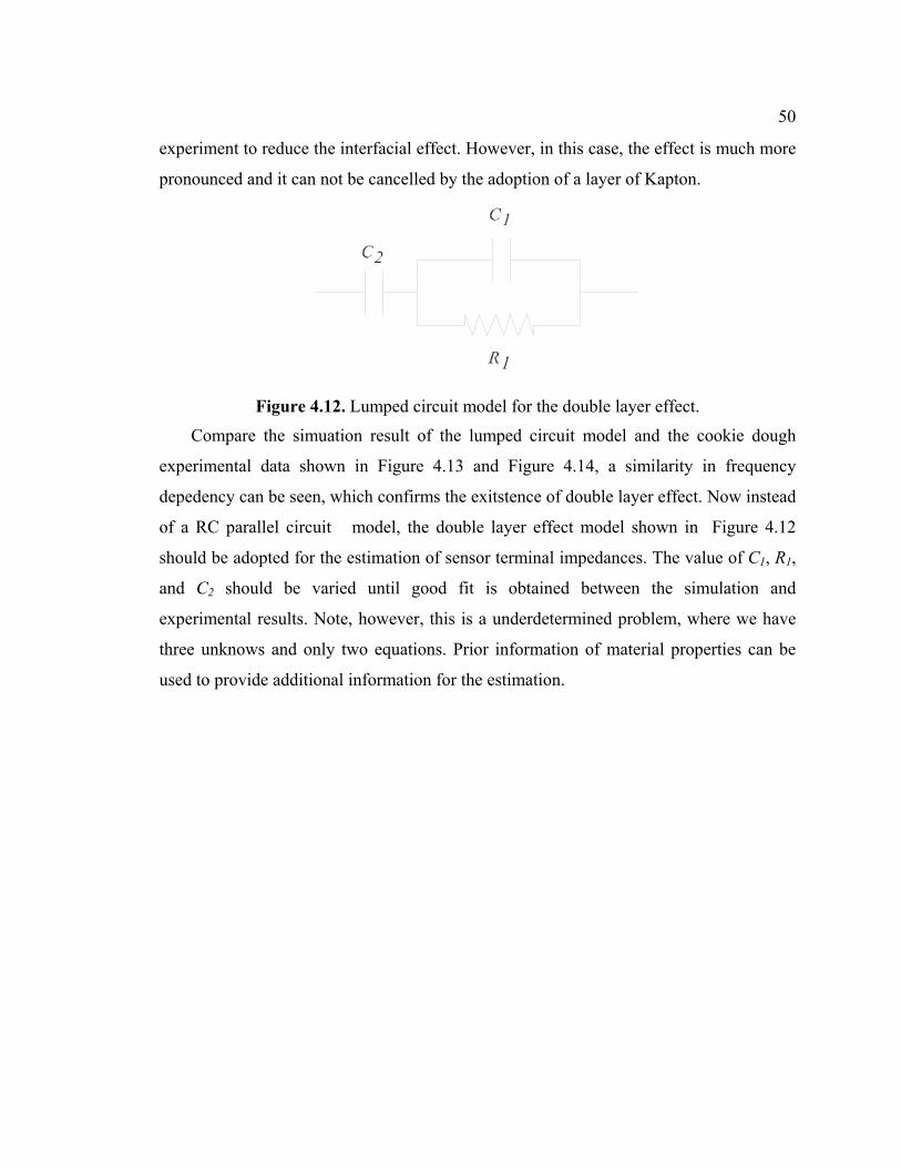
50
experiment to reduce the interfacial effect. However, in this case, the effect is much more
pronounced and it can not be cancelled by the adoption of a layer of Kapton.
Figure 4.12. Lumped circuit model for the double layer effect.
Compare the simuation result of the lumped circuit model and the cookie dough
experimental data shown in Figure 4.13 and Figure 4.14, a similarity in frequency
depedency can be seen, which confirms the exitstence of double layer effect. Now instead
of a RC parallel circuit model, the double layer effect model shown in Figure 4.12
should be adopted for the estimation of sensor terminal impedances. The value of C1, R1,
and C2 should be varied until good fit is obtained between the simulation and
experimental results. Note, however, this is a underdetermined problem, where we have
three unknows and only two equations. Prior information of material properties can be
used to provide additional information for the estimation.

51
102 103 104 105100
150
200
250
300
Frequency (Hz)
Cap
acta
nce
(pF)
102 103 104 1050
0.5
1
1.5 x 10⁻⁵
Frequency (Hz)
Con
duct
ance
(S)
102 103 104 1050
0.2
0.4
0.6
0.8
1 x 10⁻⁴
Frequency (Hz)
Cur
rent
(Am
p)
102 103 104 105-90
-80
-70
-60
-50
-40
Frequency (Hz)
Pha
se (d
eg)
33 deg78 deg87 deg
Figure 4.13. Frequency dependency of the lumped circuit model.
102 1040
1
2
3
4
5
Frequency (Hz)
Cap
acita
nce
(pF)
102 10410-12
10-10
10-8
10-6
Frequency (Hz)
Con
duct
ance
(S)
102 10410-9
10-8
10-7
10-6
Frequency (Hz)
Cur
rent
(Am
p)
102 104-80
-60
-40
-20
0
Frequency (Hz)
Phas
e (d
eg)
Figure 4.14. Frequency dependency of the lumped circuit model.

52
4.7. Simulating the manufacturing process – the rotating table To simulate the cookie manufacturing process, the rotating table setup, as shown in
Figure 4.15, is designed. Samples can be positioned on the plate with computer
controllable rotational motion. A fringing field sensor is attached to a platform, whose
vertical motion is controllable. Efforts are under way to design a automatic scanner,
where the sesnor can move according to a programmed trace and collect data at different
positions.
Figure 4.15. The rotating table setup.
4.8. The chemometric challenge – temperature and moisture control chamber
Ambient temperature is the major disturbance factor for this moisture sensing application.
Information on the moisture content is coupled with effect of temperature effect and it is
usually difficult to estimate accurately the change in moisture content in the presence of
temperature variations.
Figure 4.16 shows a moisture and temperature control chamber where the ambient
moisture concention and temperature can be independently controlled. This chamber is
ideal for running single variable experiments.

53
Figure 4.16. Moisture and temperature control chamber.
4.9. Conclusions Due to the strong correlation between material moisture concentration and its dielectric
properties, dielectrometry measurements were used for sensing cookie moisture content.
The optimized concentric sensor head enables measurement at different locations of the
sample. Impedance data shows a nearly linear dependence on moisture content. The
sensor is calibrated based on a linear model and real-time moisture content imaging is
achieved.
In this investigation, moisture content is determined from the impedance
measurements of the material of interest, without calculating the distribution of the
complex dielectric permittivity ε*. Impedance spectroscopy is shown to be adequate for a
controlled experiment. Future work is likely to involve implementation of inverse
problem solution methods to determine the spatial distribution of ε*. Efforts are
underway to integrate fringing sensors into the current setup, which involves new sensor
design and modeling. The quantitative effect of temperature variation is being
investigated so that it could be incorporated into the current calibration algorithm.

54
Chapter 5. Measuring Physical Properties of Pharmaceutical Samples
5.1. Problem statement If process control is important for the food industry, it is much more so for the
pharmaceutical industry. The Food and Drug Administration (FDA) has very stringent
regulations for pharmaceutical products in such aspects as active ingredient
concentration, tablet hardness, and coating thickness. To keep their reputations intact,
pharmaceutical manufacturers always consider quality control as their top priority.
The major obstacle for quality control of pharmaceutical products is the absence of
an accurate, efficient, and non-invasive sensing technique. The physical properties of
pharmaceutical samples are often measured by destructive tests, if they are measurable at
all. In cases where the manufacturers are not sure their products meet FDA standards,
they would rather sacrifice those products, than risking jeopardizing their reputation.
5.2. Motivation It is important to control when, where, and how much of pharmaceutical ingredients
dissolve in the body of a patient. Tablet hardness, coating thickness, and coating
roughness are among the physical parameters that determine these factors. For example,
tablet hardness and surface roughness are directly related to how fast the coating
dissolves in the body. Accurate sensing and control of these physical parameters are
crucial to obtaining the desired process of drug uptake.
This chapter investigates the feasibility of applying the non-invasive dielectrometry
sensing technique to quality control of such physical properties as tablet hardness,
coating thickness, and API content of powder samples. Tests of drug signatures are also
carried out to differentiate between unpolished, polished, and placebo tablet samples. The
results show good measurement sensitivity to parameters of interest. More extensive
experiments have to be conducted to quantify the dependencies between these physical
properties and the electrical measurements and compensate for disturbance factors.
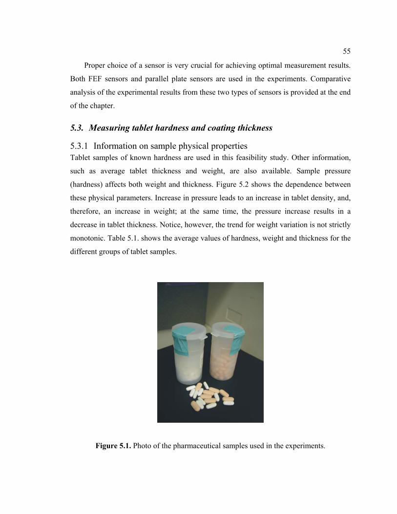
55
Proper choice of a sensor is very crucial for achieving optimal measurement results.
Both FEF sensors and parallel plate sensors are used in the experiments. Comparative
analysis of the experimental results from these two types of sensors is provided at the end
of the chapter.
5.3. Measuring tablet hardness and coating thickness
5.3.1 Information on sample physical properties Tablet samples of known hardness are used in this feasibility study. Other information,
such as average tablet thickness and weight, are also available. Sample pressure
(hardness) affects both weight and thickness. Figure 5.2 shows the dependence between
these physical parameters. Increase in pressure leads to an increase in tablet density, and,
therefore, an increase in weight; at the same time, the pressure increase results in a
decrease in tablet thickness. Notice, however, the trend for weight variation is not strictly
monotonic. Table 5.1. shows the average values of hardness, weight and thickness for the
different groups of tablet samples.
Figure 5.1. Photo of the pharmaceutical samples used in the experiments.

56
Figure 5.2. Tablet sample weight and thickness against sample pressure.
Table 5.1. Tablet sample physical properties: hardness, weight, thickness.
Sample Hardness Weight Thickness
Sample #1 25.6 (kp) 0.592 (mg) 5.56 (mm)
Sample #2 31.5 (kp) 0.607 (mg) 5.53 (mm)
Sample #3 34.3 (kp) 0.610 (mg) 5.49 (mm)
Sample #4 41.8 (kp) 0.609 (mg) 5.27 (mm)
Sample #5 45.1 (kp) 0.615 (mg) 5.26 (mm)
5.3.2 Experimental setup The experimental results presented here are from a parallel plate setup. Tablet samples of
the same hardness are arranged side by side with the same orientation between the two
electrodes of the sensor. The sensor is driven by a 1 V AC voltage signal from a Fluke
RCL meter. The meter measures the loop AC current and sensor terminal impedance. The
AC signal sweeps from 50 Hz to 100 Hz.

57
5.3.3 Experimental results Equations (2.4) and (2.5), show, respectively, the capacitance and conductance for a
parallel plate setup, where A is the area of the parallel plate electrode, d is the distance
between the two plates, ε0 is the dielectric permittivity of free space, εr is the relative
dielectric permittivity of the material and σ is the conductivity of the material.
As mentioned previously, the major variables that affect electrical measurements are
sample density and sample thickness. Density affects material dielectric permittivity εr
and conductivity σ while thickness affects d. Therefore, capacitance measurements are
sensitive to changes in both sample density and thickness. Phase measurements, on the
other hand, are determined by the relative ratio between real and imaginary part of the
impedance. Change in sample geometry affects capacitance and conductance
measurement in the same fashion and leaves their relative ratio constant. Therefore, phase
measurements are only dependent here on density variations.
Figure 5.3 and Figure 5.4 show respectively the capacitance and phase measurement
of the tablet samples against hardness at various frequencies. Conductance and current
measurements are omitted because no additional information is offered.
According to Figure 5.2, increase in hardness results in a rise in sample density and a
drop in sample thickness, which affects the capacitance measurements adversely. The
resulting measurement shown in Figure 5.3 is a trade-off between these two effects,
which explains why the trend is not monotonic. Phase measurement displays a monotonic
dependence on hardness and bears information only about samples density. Using the
combined information from capacitance and phase measurements, samples density and
thickness can be uniquely determined. The experiments carried out so far proved the
feasibility of the technique. More extensive experiments are needed to fully calibrate the
measurement system.

58
Figure 5.3. Capacitance measurements of 180 mg tablet samples against sample hardness.
Figure 5.4. Phase measurements of 180 mg tablet samples against sample hardness.
5.4. Measuring tablet coating thickness
5.4.1 The experimental setup Experiments are carried out using both a parallel plate sensor and fringing field sensor.
Figure 5.5 shows the FEF setup. For the parallel plate sensor setup, 10 samples are
arranged side by side with the same orientation between the two electrodes of the sensor.
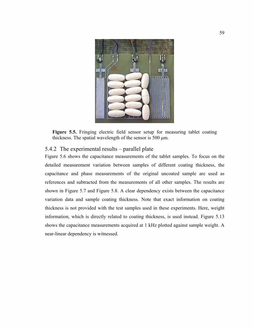
59
Figure 5.5. Fringing electric field sensor setup for measuring tablet coating thickness. The spatial wavelength of the sensor is 500 µm.
5.4.2 The experimental results – parallel plate Figure 5.6 shows the capacitance measurements of the tablet samples. To focus on the
detailed measurement variation between samples of different coating thickness, the
capacitance and phase measurements of the original uncoated sample are used as
references and subtracted from the measurements of all other samples. The results are
shown in Figure 5.7 and Figure 5.8. A clear dependency exists between the capacitance
variation data and sample coating thickness. Note that exact information on coating
thickness is not provided with the test samples used in these experiments. Here, weight
information, which is directly related to coating thickness, is used instead. Figure 5.13
shows the capacitance measurements acquired at 1 kHz plotted against sample weight. A
near-linear dependency is witnessed.

60
Figure 5.6. Absolute capacitance measurements of tablet samples with different coating thickess using a parallel plate sensor.
Figure 5.7. Capacitance variation between samples with different coating thickenss using a parallel plate sensor. The absolute capacitance measurements of the original uncoated sample are used as references.

61
102 103 104 105-0.5
0
0.5
1
1.5
2
2.5
3
3.5
Frequency (Hz)
Pha
se v
aria
tion
(deg
)
27 mg30 mg33 mg36 mgfinal
Figure 5.8. Phase variation for tablet samples with different coating thickness using a parallel plate sensor. The absolute phase measurements of the original uncoated sample are used as references.
Figure 5.9. Capacitance variation against sample weight using a parallel plate sensor.

62
5.4.3 The experimental results – fringing field Figure 5.10 shows the capacitance measurements of the samples from the fringing field
setup. A much greater difference is witnessed in this case between the measurements of
the original tablets and those of the coated ones than in the case of the parallel plate
setup. This is easily explained by the higher sensitivity of FEF sensors to the layer of
samples in direct contact with the electrodes. Again, using the measurements from the
original tablets as references, the capacitance and phase variations of the coated tablets
are calculated. The results are shown in Figure 5.11 and Figure 5.12. Figure 5.13 shows
the capacitance variation data at 1 kHz plotted against sample weight. Compared with the
parallel plate result shown in Figure 5.9, the dependency between capacitance and sample
weight is non-linear in the fringing field setup. This is, however, within expectation
considering the non-uniform field distribution of a FEF sensor. As coating thickness
increases, the electrical measurement sensitivity to thickness variation decreases. To
attain an optimal sensitivity curve, a wavelength of the FEF sensor has to be carefully
chosen. The sensor used here provided 3 different channels with various wavelengths.
The spatial wavelength of the channel used in the experiments is 500 µm, which
corresponds to a penetration depth of around 160 µm.

63
102 103 104 1057.2
7.4
7.6
7.8
8
8.2
8.4
8.6
8.8
9
Frequency (Hz)
Cap
acita
nce
(pF)
Original27 mg30 mg33 mg36 mgfinal
Figure 5.10. Absolute capacitance measurements for tablet samples with different coating thickness using a fringing electric field sensor with spatial wavelengh of 500 µm.
102 103 104 1050.2
0.3
0.4
0.5
0.6
0.7
0.8
0.9
1
1.1
1.2
Frequency (Hz)
Cap
acita
nce
varia
tion
(pF) 27 mg
30 mg33 mg36 mgfinal
Figure 5.11. Capacitance variation for tablet samples with different coating thickness using a fringing electric field sensor with spatial wavelengh of 500 µm. The absolute capacitance measurements of the original uncoated sample are used as references.

64
102 103 104 1050
0.5
1
1.5
2
2.5
3
3.5
Frequency (Hz)
Pha
se v
aria
tion
(deg
) 27 mg30 mg33 mg36 mgfinal
Figure 5.12. Phase variation for tablet samples with different coating thickness using a fringing electric field sensor with spatial wavelengh of 500 µm. The absolute phase measurements of the original uncoated sample are used as references.
26 28 30 32 34 36 38 40 42
0.44
0.46
0.48
0.5
0.52
Weight (mg)
Cap
acita
nce
var
iatio
n (p
F)
Figure 5.13. Capacitance variation against sample weight for the fringing electric field setup. The absolute capacitance measurements of the original uncoated sample are used as references.

65
5.5. Acquiring drug signature using a FEF sensor There exist the need for a non-invasive sensing technique that can differentiate different
types of drugs. One of the solutions is to look at the spectroscopy meassurements of the
drug samples in frequeny domain. Information on both the absolute value and the trend of
the frequency dependencies of the electrical measurements can be used to different types
of drugs from each other.
This section investigates the feasibility of acquiring drug signatures using the
fringing field dielectrometry sensing technique. Figure 5.14 shows the experimental
setup, where eight tablet samples are positioned on a FEF sensor with spatial wavelength
of 500 µm. The goal of the experiment is to differentiate between three groups of tablet
samples: the original, the polished, and the placebos.
Figure 5.14. Fringing electric field sensor setup for acquiring drug signature. The spatial wavelength of the sensor is 500 µm.
Figure 5.15 and Figure 5.16 show respectively the capacitance and phase
measurements of the three types of tablets. A great difference is witnessed between the
measurements of the original tablets and those of the other two types of tablets, which
makes the original tablets easily distinguishable. The measurement results for the
placebos are close to those of the polished samples, the difference in capacitance
measurements being in the range of 0.01 pF. High measurement resolution is necessary
to differentiate these two groups of samples.

66
102 103 104 1056.5
6.6
6.7
6.8
6.9
7
7.1
7.2
7.3
Frequency (Hz)
Cap
acita
nce
(pF)
OriginalPolishedPlacebo
Figure 5.15. Capacitance measurements of three different types of tablet samples using a fringing electric field sensor with spatial wavelength of 500 µm.
102 103 104 105-90.5
-90
-89.5
-89
-88.5
-88
-87.5
Frequency (Hz)
Phas
e (d
eg)
OriginalPolishedPlacebo
Figure 5.16. Phase measurements of three different types of tablet samples using a fringing electric field sensor with spatial wavelength of 500 µm.

67
5.6. Choice of sensors – FEF vs. parallel plate One of the major differences between FEF and parallel plate sensors is their different
levels of sensitivity to surface contact disturbances. Parallel plate sensors are generally
much more robust to surface contact disturbances than FEF sensors, and they should be
used when the effect of the parameters of interest is very subtle and the surface contact
uncertainties need to be reduced.
To compare the measurement performance of the FEF and parallel plate setup, the
capacitance measurements from section 5.4 are normalized. Normalization is carried out
by dividing all tablet measurements with the sensor capacitance measurements in air. The
resulting measurements are shown in Figure 5.17 and Figure 5.18. The parallel plate
setup provides greater overall measurement sensitivity to coating thickness variations.
The parallel plate setup also has better linearity, as illustrated by Figure 5.7 and Figure
5.9. Therefore for this application, the parallel plate setup is preferable to the fringing
field setup.

68
102 103 104 1052.1
2.15
2.2
2.25
2.3
2.35
2.4
2.45
2.5
2.55
2.6
Frequency (Hz)
Nor
mal
ized
cap
acita
nce
Original27 mg30 mg33 mg36 mgFinal
Figure 5.17. Normalized capacitance of tablet samples with different coating thickness using the parallel plate setup. Normalization is carried out by dividing measurements for the tablets by sensor measurements in air.

69
102 103 104 1051.15
1.2
1.25
1.3
1.35
1.4
Frequency (Hz)
Nor
mal
ized
cap
acita
nce
Original27 mg30 mg33 mg36 mgFinal
Figure 5.18. Normalized capacitance of tablet samples with different coating thickness using the fringing field setup. Normalization is carried out by dividing tablet measurements by sensor measurements in air.
Sometimes, however, the high sensitivity of FEF sensors to surface contact quality
can also be used to our advantage. For example, in section 5.5, experiments are
conducted to distinguish between unpolished and polished drug samples. Due to FEF
sensors higher sensitivity to surface contact qualities, a much more pronounced
difference is witnessed in the measurements from FEF sensors.
5.7. Measuring API concentration for powder samples This section investigates the feasibility of non-invasive monitoring of the drying process
for pharmaceutical powder samples. The electrical impedance of powder samples that
have been subject to different period of drying time are measured using the impedance
spectroscopy sensing system.
Figure 5.19 and Figure 5.20 show the capacitance and phase measurement of the
various powder samples. It can be inferred from the big difference between the
measurements of ‘0 hour’ samples and ‘2 hours’ samples that most API is removed in the
first two hours of the process. Figure 5.21 shows the capacitance measurements of the
powder samples plotted against drying time at two different frequencies. The
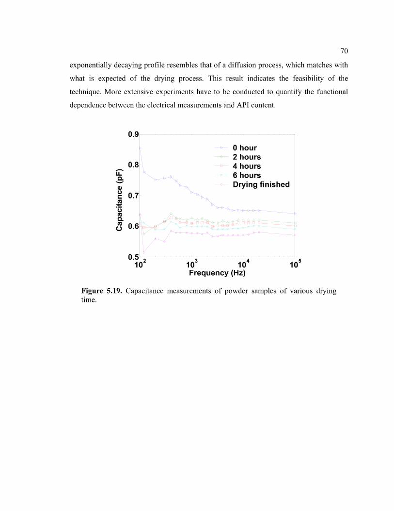
70
exponentially decaying profile resembles that of a diffusion process, which matches with
what is expected of the drying process. This result indicates the feasibility of the
technique. More extensive experiments have to be conducted to quantify the functional
dependence between the electrical measurements and API content.
Figure 5.19. Capacitance measurements of powder samples of various drying time.

71
Figure 5.20. Phase measurements of powder samples of various drying time.
Figure 5.21. Capacitance measurements of powder samples against sample drying time.
5.8. Conclusion and future work The investigation in the application of dielectrometry sensing to pharmaceutical products
included here in the thesis is still at a preliminary stage. Measurements show good
sensitivity to the parameters of interest. Sensor designs should be optimized toward the
72
particular applications to ensure the best performance. This involves such issues as
whether to use parallel plate or fringing field setup, and what geometry to use for the
electrodes.
The results presented here are obtained from carefully arranged experimental setups,
which are hard to come by if real time sensing on the production line is desired. More
practical experimental setup needs to be designed to simulate the manufacturing process,
and the effects of disturbance factors need to be investigated.
Extensive experiments need to be conducted to evaluate the repeatability of the
results. Based on these results, statistical analysis can be carried out to accurately
quantify the functional dependencies between the electrical measurements and the
parameters of interest. The functional dependencies, in turn, can be used to calibrate the
measurement system.

73
Chapter 6. Conclusions and future work
6.1. Conclusions This thesis deals with the topic of measuring material physical properties using
impedance spectroscopy. The scope of this work involves sensor design, circuit design,
software development, experiments, and data analysis. Two applications (1) moisture
sensing for cookie dough and (2) physical property sensing for pharmaceutical products
are included in the thesis. For the cookie dough application, measurement results proved
the feasibility of integration into the cookie manufacturing control process. A prototype
system is now being tested at the manufacturing site of Kraft foods. The investigation in
the pharmaceutical application is at a preliminary stage. Good measurement sensitivity
against parameters of interest is achieved. Further study needs to be carried out to study
the effect of disturbance factors, such as surface contact quality.
6.2. Directions of future work
6.2.1 Information decoupling for multivariable experiments In the case of many applications, for example, the heating process of cookie dough, more
than one material physical parameter is varying. It is necessary to measure the physical
properties other than the ones of interest and compensate for their effects. The current
experimental setup allows for simultaneous sensing of sensor arrays formed by different
types of sensor. Temperature, mass, as well as electrical impedance data can be collected
at the same time. Complex multi-variable experiments need to be carried out to help
decouple the information about different physical variables.
6.2.2 More sophisticated parameter estimation algorithms A linear dependence was assumed for the applications involved in this study. While this
model might be sufficient for the accuracy requirement of these particular applications, a
more sophisticated algorithm needs to be investigated for the generalized case of
dielectromoetry sensing applications. The major challenge lies in finding an efficient and
effective solution to the inverse problem.

74
6.2.3 Statistical evaluation of experimental results More extensive experiments need to be conducted to collect a database for the
measurement system. Statistical analysis should be carried out to test the repeatability of
the experimental results and to fully and accurately calibrate the measurement system for
each particular application.

75
End notes [1] S. O. Nelson, S. Trabelsi, and A. W. Kraszewski, "RF Sensing of Grain and Seed
Moisture Content," IEEE Sensors Journal, vol. 1, no. 2, pp. 119-126, Aug. 2001.
[2] P. M. Johnson, D. V. Thiel, and D. A. James, "Contributions to the Measured
Capacitance by the Dielectric Properties of Water in Insulated Electrode Soil
Moisture Sensors," Sensors Proceedings of IEEE, vol. 1, 2002, pp. 495-498.
[3] S. Simula, S. Ikalailen, K. Niskanen, T. Varpula, H. Seppa, and A. Paukku,
"Measurement of the Dielectric Properties of Paper," Imaging Science and
Technology, vol. 43, no. 5, pp. 472-477, 1999.
[4] A. V. Mamishev, Y. Du, B. C. Lesieutre, and M. Zahn, "Measurement of Moisture
Spatial Profiles in Transformer Pressboard," IEEE Conference on Electrical
Insulation and Dielectric Phenomena, 1998, pp. 323-326.
[5] K. Asami, T. Yonezawa, H. Wakamatsu, and N. Koyanagi, "Dielectric
Spectroscopy of Biological Cells," Bioelectrochemistry and Bioenergetics, vol. 40,
no. 2, pp. 141-145, Aug. 1996.
[6] H. Beving and G. Eriksson, "Dielectric-Spectroscopy of Human Blood," European
Journal of Surgery, pp. 87-89, 1994.
[7] D. D. Denton, J. B. Camou, and S. D. Senturia, "Effects of Moisture Uptake on the
Dielectric Permittivity of Polyimide Films," Proceedings of the 1985 International
Symposium on Moisture and Humidity, 1985, pp. 505-513.
[8] A. V. Mamishev, Y. Du, B. C. Lesieutre, and M. Zahn, "Development and
Applications of Fringing Electric Field Sensors and Parameter Estimation
Algorithms," Journal of Electrostatics, vol. 46, pp. 109-123, 1999.
76
[9] I. C. Shay and M. Zahn, "Cylindrincal Geometry Electroquasistatic Dielectrometry
Sensors," IEEE Conference on Electrical Insulation and Dielectric Phenomena,
2002, pp. 126-129.
[10] W. L. Kerr, R. J. Kauten, M. Ozilgen, M. J. McCarthy, and D. S. Reid, "NMR
Imaging, Calorimetric, and Mathematical Modeling Studies of Food Freezing,"
Journal of Food Process Engineering, vol. 19, no. 4, pp. 363-384, Nov. 1996.
[11] B. P. Hills, J. Godward, and K. M. Wright, "Fast Radial NMR Microimaging
Studies of Pasta Drying," Journal of Food Engineering, vol. 33, no. 3-4, pp. 321-
335, Aug. 1997.
[12] C. Simoneau, M. J. McCarthy, and J. B. German, "Magnetic-Resonance-Imaging
and Spectroscopy for Food Systems," Food Research International, vol. 26, no. 5,
pp. 387-398, 1993.
[13] M. Kalab, P. Allanwojtas, and S. S. Miller, "Microscopy and Other Imaging
Techniques in Food Structure-Analysis," Trends in Food Science & Technology,
vol. 6, no. 6, pp. 177-186, June 1995.
[14] M. J. McCarthy and K. L. McCarthy, "Applications of Magnetic Resonance
Imaging to Food Research," Magnetic Resonance Imaging, vol. 14, no. 7-8, pp.
799-802, 1996.
[15] S. J. Schmidt, X. Z. Sun, and J. B. Litchfield, "Applications of Magnetic Resonance
Imaging in Food Science," Critical Reviews in Food Science and Nutrition, vol. 36,
no. 4, pp. 357-385, 1996.
[16] M. Riva and S. Liviero, "Image Analysis Approach to Characterise the Bread
Cooking Kinetic," Industrie Alimentari, vol. 39, no. 395, pp. 953-960, Sept. 2000.
[17] D. D. Shepard and K. R. Smith, "Ultrasonic Cure Monitoring of Advanced
Composites," Sensor Review, vol. 19, no. 3, pp. 187-191, 1999.
77
[18] L. C. Haynes and J. P. Locke, "Microwave Permittivities Of Cracker Dough, Starch
and Gluten," Journal of Microwave Power and Electromagnetic Energy, vol. 30,
no. 2, pp. 124-131, 1995.
[19] R. Neimanis, H. Lennholm, and R. Eriksson, "Determination Of Moisture Content
in Impregnated Paper Using Near Infrared Spectroscopy," Electrical Insulation And
Dielectric Phenomena, 1999, pp. 162-165.
[20] Y. R. Kim, M. T. Morgan, M. R. Okos, and R. L. Stroshine, "Measurement And
Prediction Of Dielectric Properties of Biscuit Dough At 27MHz," Journal of
Microwave Power and Electromagnetic Energy, vol. 33, no. 3, pp. 184-194, 1998.
[21] M. Craig and S. Tamburic, "Dielectric Analysis of Bioadhesive Gel Systems,"
European Journal of pharmaceutics and biopharmaceutics, vol. 44, no. 1, pp. 61-
70, 1997.
[22] M. Craig, "Dielectric Spectroscopy As a Novel Analytical Technique Within the
Pharmaceutical Sciences," STP-Pharma-Pratiques, vol. 5, no. 6, pp. 421-42, 1995.
[23] G. W. Bak, K. H. Bodek, B. Hilczer, and T. Pawlowski, "Thermal Aging
Phenomena in Chitosan-Related Pharmaceutical Systems," IEEE Transactions on
Dielectrics and Electrical Insulation, vol. 8, no. 3, pp. 555-558, 2001.
[24] N. F. Sheppard, D. R. Day, H. L. Lee, and S. D. Senturia, "Microdielectrometry,"
Sensors and Actuators, vol. 2, no. 3, pp. 263-274, July 1982.
[25] V. J. Lumelsky, M. S. Shur, and S. Wagner, "Sensitive Skin," IEEE Sensors
Journal, vol. 1, pp. 41-51, Mar. 2001.
[26] A. K. Jonscher, Universal Relaxation Law, Chelsea Dielectrics Press London, 1996.
[27] A. R. von Hippel, Dielectrics and Waves, John Wiley & Sons, 1954.
78
[28] A. K. Jonscher, Dielectric Relaxation in Solids, Chelsea Dielectrics Press London,
1983.
[29] w. R. Westphal, "Permittivity, Distributed Circuits," in von Hippel, A. (ed.)
Dielectric materials and applications Cambridge: The M.I.T. press, 1961, pp. 63-
122.
[30] A. V. Mamishev, A. R. Takahashi, Y. Du, B. C. Lesieutre, and M. Zahn,
"Parameter Estimation in Dielectrometry Measurements," Journal of Electrostatics,
vol. 56, pp. 465-492, 2002.
[31] H. Schlichtling, "Boundary-Layer Theory," 1974,
[32] F. Bellucci, I. Khamis, S. D. Senturia, and R. M. Latanision, "Moisture Effects on
the Electrical Conductivity of Kapton Polyimide," Journal of the Electrochemical
Society, vol. 137, no. 6, pp. 1778-1784, 1990.
[33] J. Melcher, Y. Daben, and G. Arlt, "Dielectric Effects of Moisture in Polyimide,"
IEEE Transactions on Electrical Insulation, vol. 24, no. 1, pp. 31-38, Feb. 1989.
[34] A. von Hippel, Dielectric Materials and Applications, Artech House, 1995.
[35] J. G. Webster, "Electrodes," in Webster, J. G. (ed.) Electrical Impedance
Tomography Bristol and New York: Adam Hilger, 1990, pp. 21-28.
[36] B. S. Mohamed, R. Z. Morawski, A. W. Kraszewski, A. Brawicz, and S. O. Nelson,
"Calibration of a Microwave System for Measuring Grain Moisture Content," IEEE
Transactions on Instrumentation and Measurements, vol. 48, no. 3, pp. 778-783,
June 1999.
[37] A. K. Vijh, "Electrochemical Nature of Metal-Insulator Interfaces," IEEE
International Symposium on Electrical Insulation, 1996, pp. 870-873.

79
[38] A. V. Mamishev, B. C. Lesieutre, and M. Zahn, "Optimization of Multi-
Wavelength Interdigital Dielectrometry Instrumentation and Algorithms," IEEE
Transactions on Dielectrics and Electrical Insulation, pp. 408-420, 1998.

80
References [1] S. O. Nelson, S. Trabelsi, and A. W. Kraszewski, "RF Sensing of Grain and Seed
Moisture Content," IEEE Sensors Journal, vol. 1, no. 2, pp. 119-126, Aug. 2001.
[2] P. M. Johnson, D. V. Thiel, and D. A. James, "Contributions to the Measured
Capacitance by the Dielectric Properties of Water in Insulated Electrode Soil
Moisture Sensors," Sensors Proceedings of IEEE, vol. 1, 2002, pp. 495-498.
[3] S. Simula, S. Ikalailen, K. Niskanen, T. Varpula, H. Seppa, and A. Paukku,
"Measurement of the Dielectric Properties of Paper," Imaging Science and
Technology, vol. 43, no. 5, pp. 472-477, 1999.
[4] A. V. Mamishev, Y. Du, B. C. Lesieutre, and M. Zahn, "Measurement of Moisture
Spatial Profiles in Transformer Pressboard," IEEE Conference on Electrical
Insulation and Dielectric Phenomena, 1998, pp. 323-326.
[5] K. Asami, T. Yonezawa, H. Wakamatsu, and N. Koyanagi, "Dielectric
Spectroscopy of Biological Cells," Bioelectrochemistry and Bioenergetics, vol. 40,
no. 2, pp. 141-145, Aug. 1996.
[6] H. Beving and G. Eriksson, "Dielectric-Spectroscopy of Human Blood," European
Journal of Surgery, pp. 87-89, 1994.
[7] D. D. Denton, J. B. Camou, and S. D. Senturia, "Effects of Moisture Uptake on the
Dielectric Permittivity of Polyimide Films," Proceedings of the 1985 International
Symposium on Moisture and Humidity, 1985, pp. 505-513.
[8] A. V. Mamishev, Y. Du, B. C. Lesieutre, and M. Zahn, "Development and
Applications of Fringing Electric Field Sensors and Parameter Estimation
Algorithms," Journal of Electrostatics, vol. 46, pp. 109-123, 1999.

81
[9] I. C. Shay and M. Zahn, "Cylindrincal Geometry Electroquasistatic Dielectrometry
Sensors," IEEE Conference on Electrical Insulation and Dielectric Phenomena,
2002, pp. 126-129.
[10] W. L. Kerr, R. J. Kauten, M. Ozilgen, M. J. McCarthy, and D. S. Reid, "NMR
Imaging, Calorimetric, and Mathematical Modeling Studies of Food Freezing,"
Journal of Food Process Engineering, vol. 19, no. 4, pp. 363-384, Nov. 1996.
[11] B. P. Hills, J. Godward, and K. M. Wright, "Fast Radial NMR Microimaging
Studies of Pasta Drying," Journal of Food Engineering, vol. 33, no. 3-4, pp. 321-
335, Aug. 1997.
[12] C. Simoneau, M. J. McCarthy, and J. B. German, "Magnetic-Resonance-Imaging
and Spectroscopy for Food Systems," Food Research International, vol. 26, no. 5,
pp. 387-398, 1993.
[13] M. Kalab, P. Allanwojtas, and S. S. Miller, "Microscopy and Other Imaging
Techniques in Food Structure-Analysis," Trends in Food Science & Technology,
vol. 6, no. 6, pp. 177-186, June 1995.
[14] M. J. McCarthy and K. L. McCarthy, "Applications of Magnetic Resonance
Imaging to Food Research," Magnetic Resonance Imaging, vol. 14, no. 7-8, pp.
799-802, 1996.
[15] S. J. Schmidt, X. Z. Sun, and J. B. Litchfield, "Applications of Magnetic Resonance
Imaging in Food Science," Critical Reviews in Food Science and Nutrition, vol. 36,
no. 4, pp. 357-385, 1996.
[16] M. Riva and S. Liviero, "Image Analysis Approach to Characterise the Bread
Cooking Kinetic," Industrie Alimentari, vol. 39, no. 395, pp. 953-960, Sept. 2000.
[17] D. D. Shepard and K. R. Smith, "Ultrasonic Cure Monitoring of Advanced
Composites," Sensor Review, vol. 19, no. 3, pp. 187-191, 1999.

82
[18] L. C. Haynes and J. P. Locke, "Microwave Permittivities Of Cracker Dough, Starch
and Gluten," Journal of Microwave Power and Electromagnetic Energy, vol. 30,
no. 2, pp. 124-131, 1995.
[19] R. Neimanis, H. Lennholm, and R. Eriksson, "Determination Of Moisture Content
in Impregnated Paper Using Near Infrared Spectroscopy," Electrical Insulation And
Dielectric Phenomena, 1999, pp. 162-165.
[20] Y. R. Kim, M. T. Morgan, M. R. Okos, and R. L. Stroshine, "Measurement And
Prediction Of Dielectric Properties of Biscuit Dough At 27MHz," Journal of
Microwave Power and Electromagnetic Energy, vol. 33, no. 3, pp. 184-194, 1998.
[21] M. Craig and S. Tamburic, "Dielectric Analysis of Bioadhesive Gel Systems,"
European Journal of pharmaceutics and biopharmaceutics, vol. 44, no. 1, pp. 61-
70, 1997.
[22] M. Craig, "Dielectric Spectroscopy As a Novel Analytical Technique Within the
Pharmaceutical Sciences," STP-Pharma-Pratiques, vol. 5, no. 6, pp. 421-42, 1995.
[23] G. W. Bak, K. H. Bodek, B. Hilczer, and T. Pawlowski, "Thermal Aging
Phenomena in Chitosan-Related Pharmaceutical Systems," IEEE Transactions on
Dielectrics and Electrical Insulation, vol. 8, no. 3, pp. 555-558, 2001.
[24] N. F. Sheppard, D. R. Day, H. L. Lee, and S. D. Senturia, "Microdielectrometry,"
Sensors and Actuators, vol. 2, no. 3, pp. 263-274, July 1982.
[25] V. J. Lumelsky, M. S. Shur, and S. Wagner, "Sensitive Skin," IEEE Sensors
Journal, vol. 1, pp. 41-51, Mar. 2001.
[26] A. K. Jonscher, Universal Relaxation Law, Chelsea Dielectrics Press London, 1996.
[27] A. R. von Hippel, Dielectrics and Waves, John Wiley & Sons, 1954.

83
[28] A. K. Jonscher, Dielectric Relaxation in Solids, Chelsea Dielectrics Press London,
1983.
[29] w. R. Westphal, "Permittivity, Distributed Circuits," in von Hippel, A. (ed.)
Dielectric materials and applications Cambridge: The M.I.T. press, 1961, pp. 63-
122.
[30] A. V. Mamishev, A. R. Takahashi, Y. Du, B. C. Lesieutre, and M. Zahn,
"Parameter Estimation in Dielectrometry Measurements," Journal of Electrostatics,
vol. 56, pp. 465-492, 2002.
[31] H. Schlichtling, "Boundary-Layer Theory," 1974,
[32] F. Bellucci, I. Khamis, S. D. Senturia, and R. M. Latanision, "Moisture Effects on
the Electrical Conductivity of Kapton Polyimide," Journal of the Electrochemical
Society, vol. 137, no. 6, pp. 1778-1784, 1990.
[33] J. Melcher, Y. Daben, and G. Arlt, "Dielectric Effects of Moisture in Polyimide,"
IEEE Transactions on Electrical Insulation, vol. 24, no. 1, pp. 31-38, Feb. 1989.
[34] A. von Hippel, Dielectric Materials and Applications, Artech House, 1995.
[35] J. G. Webster, "Electrodes," in Webster, J. G. (ed.) Electrical Impedance
Tomography Bristol and New York: Adam Hilger, 1990, pp. 21-28.
[36] B. S. Mohamed, R. Z. Morawski, A. W. Kraszewski, A. Brawicz, and S. O. Nelson,
"Calibration of a Microwave System for Measuring Grain Moisture Content," IEEE
Transactions on Instrumentation and Measurements, vol. 48, no. 3, pp. 778-783,
June 1999.
[37] A. K. Vijh, "Electrochemical Nature of Metal-Insulator Interfaces," IEEE
International Symposium on Electrical Insulation, 1996, pp. 870-873.

84
[38] A. V. Mamishev, B. C. Lesieutre, and M. Zahn, "Optimization of Multi-
Wavelength Interdigital Dielectrometry Instrumentation and Algorithms," IEEE
Transactions on Dielectrics and Electrical Insulation, pp. 408-420, 1998.
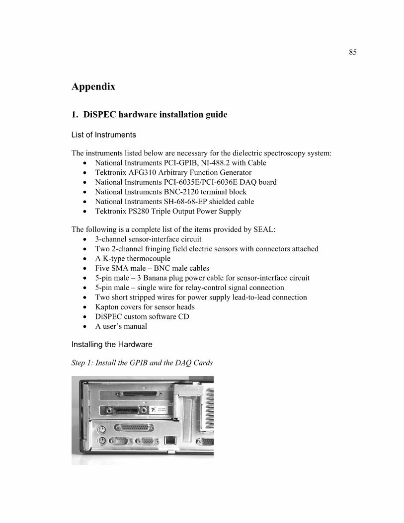
85
Appendix
1. DiSPEC hardware installation guide List of Instruments
The instruments listed below are necessary for the dielectric spectroscopy system:
• National Instruments PCI-GPIB, NI-488.2 with Cable • Tektronix AFG310 Arbitrary Function Generator • National Instruments PCI-6035E/PCI-6036E DAQ board • National Instruments BNC-2120 terminal block • National Instruments SH-68-68-EP shielded cable • Tektronix PS280 Triple Output Power Supply
The following is a complete list of the items provided by SEAL:
• 3-channel sensor-interface circuit • Two 2-channel fringing field electric sensors with connectors attached • A K-type thermocouple • Five SMA male – BNC male cables • 5-pin male – 3 Banana plug power cable for sensor-interface circuit • 5-pin male – single wire for relay-control signal connection • Two short stripped wires for power supply lead-to-lead connection • Kapton covers for sensor heads • DiSPEC custom software CD • A user’s manual
Installing the Hardware Step 1: Install the GPIB and the DAQ Cards

86
Plug the NI GPIB and the NI-DAQ boards into the experimental computer and install
all recommended drivers.
Step 2: Connect BNC-2120 to the DAQ Board
Connect BNC-2120 breakout box to the DAQ card in the computer using the shielded
SH-68-68-EP cable.
Step 3: Connect Thermocouple to BNC-2120
Plug thermocouple into the thermocouple socket of the BNC-2120 breakout box.
Check that the row switches for ACH0 and ACH1 are set to the right, the “Temp.Ref.” and “Thermocouple” positions.

87
Step 4: Connect the Sensor Box to BNC-2120 Attach the BNC-ends of four BNC-SMA cables to BNC-2120’s channels ACH2-
ACH5. The switches under all ACH connectors should be in GS position.
Switch ACH3 selector (above the thermocouple connector) to BNC position.
Using the BNC-SMA cables to connect the ADC0 to ADC3 terminals on the sensor interface box to the ACH2 to ACH5 of BNC-2120.

88
Place the sensor interface box and the sensor as far away as possible from the
computer, the monitor and other electronic devices to minimize noise interference.
Step 5: Connect the Relay Control Lead to BNC-2120 Connect the relay-control wire from the “Cntrl.” socket of sensor interface box to
DIO0 of BNC-2120 using a 5-pin to single wire connector.

89
To connect the wire to BNC-2120 DIO0 port, untighten a screw (on the right), let the wire end into the hole and re-tighten the screw.
Step 6: Set up the Power Supply
To properly set the polarity of the power supply, two short wires should be
connecting the outputs as shown in the picture below:
Set the power supply to independent mode by adjusting the two buttons in the middle
of the front panel. Set the display-mode switches to Voltage position. The current dial should be set to the twelve-o’clock position (halfway). Use voltage dials to set both outputs to 10 volts. DO NOT CHANGE THE VOLTAGE SETTINGS WHILE THE SENSOR INTERFACE IS CONNECTED TO THE POWER SUPPLY! Once the voltage is set, connect the interface box to the power supply using 5-pin to 3 banana plug cable.
The plug labeled GND can be connected to either of the two ground sockets available on the power supply. Connect the “+” plug to the “+” terminal of the right 0-20V supply and “-“ plug to the “-“ terminal of the left 0-20V supply.
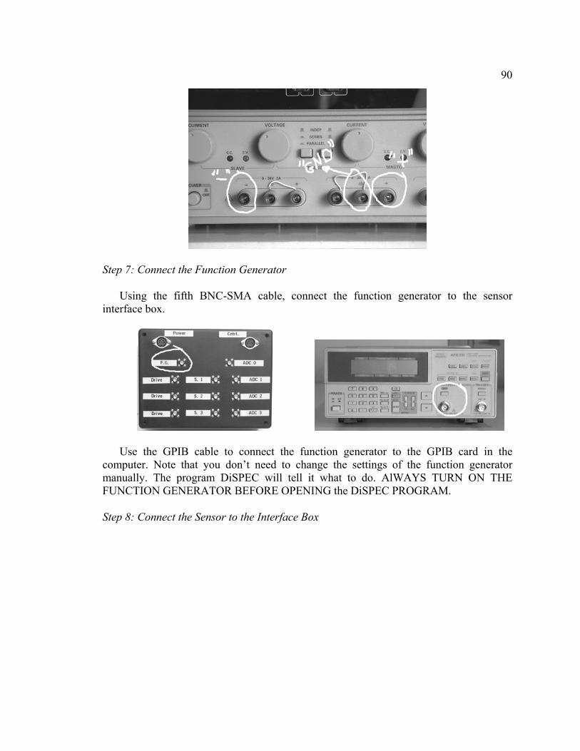
90
Step 7: Connect the Function Generator Using the fifth BNC-SMA cable, connect the function generator to the sensor
interface box.
Use the GPIB cable to connect the function generator to the GPIB card in the computer. Note that you don’t need to change the settings of the function generator manually. The program DiSPEC will tell it what to do. AlWAYS TURN ON THE FUNCTION GENERATOR BEFORE OPENING the DiSPEC PROGRAM.
Step 8: Connect the Sensor to the Interface Box

91
The sensor is connected to the interface as follows: The cable labeled as “drive” of
the sensor is connected to any of the Drive terminals of the board. The ones labeled as “inner sense” and “outer sense” are connected to the S. 1 and S. 2 terminals on the sensor interface box respectively. 2. DiSPEC software guide Installing the Software This LABVIEW application is for viewing data in real time as well as recording data to a file. Start by opening the DiSPEC folder on the CD. Go to folder “Installer” and double click on the “setup” icon. Follow the setup guide step by step and the software will be installed on your computer. After installation, the program will show up in your computer’s start up menu as DiSPEC. Using the Software After all the hardware is installed, go to the start up menu of your computer and open the program DiSPEC. The following steps need to be followed to run the software.
1. Connect all the instruments according to the instructions in the hardware guide. 2. Open the NI software “Measure & Automation Explorer” (MAX). (The software
should be provided the DAQ board). Find out the device number for the function generator and the DAQ board. Specific instructions are available below under Device Number of the Function Generator and the DAQ Board.
3. Go to the system settings tab in the front panel and enter the device numbers found from step 1. The same values need to be manually entered each time the program is opened if they are found to be different from the default values.
4. Find out the time delay for each channel of the circuit board. For detailed instructions, go to Time Delay.

92
5. Enter the time delay values obtained from step 3 in the system settings tab. Note that if found to be different from the default values, these time delay constants have to be reentered each time the program is opened.
6. Go to the Controls tab, and configure the entries in the tab. For detailed instructions, go to Controls.
7. Turn on the function generator and the power supply. 8. Press the “Run” and the “Acquire” button. If an arrow appears on the top left
corner of the front panel, click on the arrow and the program will start running. If the arrow doesn’t appear, the code should already be running after the “Run” and the “Acquire” button is pressed down.
9. Go to the different tabs on the front panel to look at the data and the graphs. 10. To monitor change in sample capacitance more visually, go to the Real-time
Imaging tab. 11. To stop the program, press the “Acquire” button again.
Configure the System In the front panel, go to the “System Settings” tab, a window like the following will show up.

93
Back
Upon starting LABVIEW, the 'System settings' has all its entry values set to their defaults for the 2 channel fringing field sensor. The values should be the same as those shown in Error! Reference source not found.. These default values should be used unless specified otherwise below. Description of the entries can be obtained by right-clicking on an entry and selecting “Descriptions and Tips” on the menu.
Device Number of the Function Generator and the DAQ Board The device numbers of the function generator and the DAQ board are dependent on the particular setup, therefore values different from those specified as default may need to be used. To get the device numbers, open the NI software “Measurement & Automation Explorer” that is provided with the DAQ board. Double click on “Devices and Interfaces”, the DAQ board and the NI GPIB card will show up. The number listed for the DAQ board is the device number for the DAQ and the number listed for the GPIB card is the device number for the function generator.
Back
Channel Numbers on the DAQ board
94
This entry specifies the channel numbers on the DAQ board that the input and the three output signals of the circuit are connected to. The default values are “2,3,4,5”. Channels 0 and 1 on the DAQ board are saved for the thermocouple. The first channel number is the input to the DAQ board, and the following numbers are output channels, displayed in front channel as channels 1, 2, and 3 respectively. All numbers must be separated by commas. (Channel 3 is most often used in the parallel plate setup rather than the fringing field system)
Reference Capacitance The “Reference Capacitance” entries specify the reference capacitance used for each channel of the sensor circuit board. Note that these values are not the same as the values of the reference capacitors on the board. The effect of the stray capacitances (e.g. that introduced by the Op-Amp has to be accounted for.) The default values are obtained through careful calibration of the system. These values should be used unless some circuit elements are changed. Recalibration of the system is necessary if changes are made to the circuit.
Time Delay Multiplexing of the DAQ board introduces a time delay between the data stream from its different channels. The time delay causes significant phase distortion, therefore its effect has to be eliminated. Unfortunately, the time delay values are device dependent. A different computer and DAQ board will cause a change in these values, which means that these values have to be fine-tuned for each particular setup. The following procedure can be used to find the time delay constants:
1. Connect the input and all the outputs of the circuit board to the function generator. Note that since all channels are connected to the same source, ideally there should be no phase delay between the channels.
2. Run the program at the highest frequency (30 kHz). Ideally, the gain should be 1 and the phase should be zero for all channels. Adjust the time delay for each channel of the sensor in the “systems and setting” tab until the phase delays for all channels are 0.
3. The new time delay constants must be typed in manually each time the program is started.
Back
The Settings for the Thermocouple

95
Channel 0 and 1 of the DAQ board should always be used for the thermocouple as is specified in the default setting. The sampling rate for the thermocouple could be increased if an improvement in the speed of the program is desired. Otherwise, use the default value. Averaging is used here to remove noise. The number of samples for temperature averaging can be changed for different application. Controls The controls tab should look like the following window.
Back
Mass

96
Real-time monitoring of sample mass is not necessary at this point. This function is included for possible future applications. By pressing the “mass” button down, the program will acquire data from a scale that is connected to the computer through a serial port.
Temperature A K type thermocouple is connected to the computer. By pressing the “Temperature” button down, the system starts acquiring data from the thermocouple and saving the temperature data to the output file if “Saving to file” is also enabled.
Sweep When the “Sweep” button is not pressed, the system runs at a single frequency specified by the “Start Frequency” entry. The system performs frequency sweeps when the “Sweep” button is enabled. The range of the frequency sweep is defined by the start and the stop frequency. The minimum and maximum frequencies allowed by the current version of the program are 1 Hz and 30 kHz respectively. Measurements at frequencies lower than 1 Hz are comparably noisy, thus we limit the frequency to above 1 Hz. The frequency range can be easily extended for future applications.
Save to File If you wish to record the data to a file, the “Save to File” button should be pressed down. You can enter the file name and the saving directory in the “File Name” entry. If the entry is left blank, a file saving window will automatically pop up when the program starts running. The file can be saved as an Excel spreadsheet or a ‘.txt’ file.
Back
Real-time Imaging The following is a picture of the real-time imaging tab.

97
The tab provides a profile of the sample by displaying the capacitance of all channels of the sensor. Note that in a 2-channel fringing field setup, the information shown for channel 3 should be ignored. Channel 3 is included here mainly for the consideration that a 3-channel sensor might be used in the future. The capacitance values displayed in the vertical bars are all scaled to be within 0 to 1. The “Maximum Capacitance” knobs on the right refer to the actual capacitance value in “pF” when the bar displays a value of “1”. The knobs could be adjusted for the best visual effect.
Back