inductance modeling and extraction in emc applications
TRANSCRIPT

Scholars' Mine Scholars' Mine
Masters Theses Student Theses and Dissertations
2009
Inductance modeling and extraction in EMC applications Inductance modeling and extraction in EMC applications
Clint Matthew Patton
Follow this and additional works at: https://scholarsmine.mst.edu/masters_theses
Part of the Electrical and Computer Engineering Commons
Department: Department:
Recommended Citation Recommended Citation Patton, Clint Matthew, "Inductance modeling and extraction in EMC applications" (2009). Masters Theses. 5422. https://scholarsmine.mst.edu/masters_theses/5422
This thesis is brought to you by Scholars' Mine, a service of the Missouri S&T Library and Learning Resources. This work is protected by U. S. Copyright Law. Unauthorized use including reproduction for redistribution requires the permission of the copyright holder. For more information, please contact [email protected].

INDUCTANCE MODELING AND EXTRACTION
IN EMC APPLICATIONS
by
CLINT MATTHEW PATTON
A THESIS
Presented to the Faculty of the Graduate School of the
MISSOURI UNIVERSITY OF SCIENCE AND TECHNOLOGY
In Partial Fulfillment of the Requirements for the Degree
MASTER OF SCIENCE IN ELECTRICAL ENGINEERING
2009
Approved by
James Drewniak, Advisor
David Pommerenke
Mehdi Ferdowsi


iii
ABSTRACT
Inductance has become a challenging problem for EMC engineers in many
applications. Regardless of the application at hand, the first step remains the same; return
to the physics and trace the current paths.
IGBTs have become an important part in the design of power electronics because
of their ability to switch fast and with stand high currents. Modules used for three phase
motor drives often create problems when neglected parasitic components show
themselves and interfere with the performance of the desired operation of a system.
Many manufactures of these modules do not give out equivalent circuit modules and
therefore leave a black box for this part of the designers schematic used in simulations.
When these systems include motors, other problems can arise which may require their
own consideration.
Pre-emphasis is a method used to reduce the attenuation of a signal as it travels
from one end of a transmission line to another by boosting frequency components of a
signal. In order for this method to work, it is important to know how the impedance
changes across the board. Working with the capacitances is relatively easy, while
revealing the inductance and pin pointing it on the geometry often creates a challenge.
Strong magnetic fields are desired for high energy delivering systems where full-
wave modeling plays a crucial role in the design of superior systems. The inductance
associated with the geometry must be distributed properly for the development of a
system that maximizes the fields. This is accomplished by following the current paths
and focusing on the physics involved.

iv
ACKNOWLEDGMENTS
I would like to express my up most gratitude to my advisor, Dr. James Drewniak,
for the time he spent developing my skills in EMC applications. From the day I stepped
into his office looking for an undergraduate research project, he influenced my decisions
and research helping me gain confidence in my knowledge. I am also in debt to Dr.
David Pommerenke for the measurement and electronics training I received from him.
Although he was very busy, he was always willing to help me with my project. Dr. Jun
Fan and Dr. Daryl Beetner were always willing to sacrifice their time to help answer my
questions and for that I am grateful.
I am thankful for the students in the lab that helped me with projects. Hemant
helped me learn Quartus and Allegro when it would have taken me weeks to do so
otherwise. Matteo started teaching me how to use CST Microwave Studio when I was
still an undergraduate student. I want to thank the senior design students, Igor, Jason, and
Matt, who I mentored and trained as well as the senior design team and Dr. Edward
Wheeler from Rose-Hulman. They spent much time working on the Rockwell
Automation project which is a major section of my thesis.
I appreciate the funding I received from the Missouri University of Science and
Technology EMC Laboratory as a Graduate Research Assistant as well as the funding
from the Electrical Engineering Department while serving as a Teacher's Aide.
I must also thank my parents, Rick and Theresa, and my brother, Kevin, for
always supporting me while I worked on my degree. I am appreciative of my other
relatives and friends who helped me out while living in Rolla. I am in debt to my wife,
Amber, who has tolerated my devotion to the lab, classes, and research and has supported
me even though much of my time has been given to things other than her.

v
TABLE OF CONTENTS
Page
ABSTRACT ....................................................................................................................... iii
ACKNOWLEDGMENTS ................................................................................................. iv
LIST OF ILLUSTRATIONS ............................................................................................ vii
LIST OF TABLES ............................................................................................................. xi
SECTION
1. INTRODUCTION .......................................................................................................1
2. PARASITIC COMPONENTS OF IGBT MODULES ................................................3
2.1. INDUCTANCE .....................................................................................................4
2.1.1. Inductance Measurements. .............................................................................5
2.1.2. Inductance Simulations. .................................................................................6
2.2. CAPACITANCE .................................................................................................14
2.2.1. Capacitance Measurements. .........................................................................14
2.2.2. Capacitance Simulations. .............................................................................18
3. FBGA PARASITIC INDUCTANCES ......................................................................21
3.1. IMPEDANCES SEEN AT PORTS ONE AND THREE ....................................23
3.1.1. Measurements. .............................................................................................23
3.1.2. Simulations. .................................................................................................23
3.1.3. Analytical Calculations. ...............................................................................30
3.2. IMPEDANCES SEEN AT PORT TWO ............................................................37
3.2.1. Simulations. .................................................................................................37
3.2.2. Analytical Calculations. ...............................................................................37
4. LOCATING PARASITIC CIRCUIT ELEMENTS IN MOTOR DRIVES ..............39
4.1. CURRENT PROBE EFFECTS ON MEASUREMENTS ..................................39
4.1.1. Copper Strap. ...............................................................................................39
4.1.2. Current Probe Transfer Impedance. .............................................................41
4.2. MEASURED IMPEDANCE OF MOTOR DRIVE TO CABLES .....................44
4.2.1. Measurements Performed from Inside IGBT. .............................................45
4.2.2. Input Impedance Looking into the IGBT Module. ......................................48
4.2.3. IGBT Module to Cable Transfer Impedance. ..............................................48
4.2.4. Transfer Impedance Outside the IGBT Module. .........................................49
5. ENERGY DELIVERING SYSTEMS .......................................................................54

vi
5.1. PROTOTYPE ......................................................................................................55
5.1.1. Simulations. .................................................................................................55
5.1.2. Manufacturing the Printed Circuit Board. ...................................................62
5.2. NEW ONE LAYER DESIGN ............................................................................63
5.2.1. Changes Made to PCB to Eliminate Electrostatic Discharge. .....................63
5.2.2. CST Simulations Made for New Design. ....................................................65
5.2.3. Current Calculations Performed in Matlab. .................................................68
5.2.4. Manufacturing New PCB Coil Design. .......................................................72
APPENDIX ........................................................................................................................74
BIBLIOGRAPHY ............................................................................................................130
VITA ................................................................................................................................131

vii
LIST OF ILLUSTRATIONS
Page
Figure 2.1. IGBT Geometry ............................................................................................... 3
Figure 2.2. IGBT Labeled Area Fills ................................................................................. 4
Figure 2.3. Current Paths for All Three Phases ................................................................. 5
Figure 2.4. Current Path of Phase 1 ................................................................................... 6
Figure 2.5. Measurement Setup for Phase One.................................................................. 6
Figure 2.6. Simulation Model for Phase One .................................................................... 7
Figure 2.7. Phase One Impedance Comparison ................................................................. 8
Figure 2.8. Labeled Sections of Simulation Model ........................................................... 9
Figure 2.9. Phase One ADS M2 Model ............................................................................. 9
Figure 2.10. Phase One ADS M2 Model Results .............................................................. 9
Figure 2.11. Q3D Model Used to Calculate the Inductance of the Probe ....................... 10
Figure 2.12. Q3D Model Used to Calculate the Inductance of Two Bond Wires ........... 11
Figure 2.13. Q3D Model Used to Calculate the Inductance of Four Bond Wires ........... 11
Figure 2.14. Q3D Model for Self Inductance Calculation of Area Fill A ........................12
Figure 2.15. ADS Model Using Q3D Calculated Values .................................................13
Figure 2.16. Comparison of ADS Results and Measured Values .....................................13
Figure 2.17. Substrate Capacitance Measurement Setup for Center Conductor
Connection ....................................................................................................14
Figure 2.18. Substrate Capacitance Measurement Setup for Outer Conductor
Connection ....................................................................................................15
Figure 2.19. Substrate Capacitance Measurement Results ...............................................15
Figure 2.20. Substrate Dimensions ...................................................................................16
Figure 2.21. The Bond Wires were Removed from the IGBT Module to Measure
the Capacitance of the Major Area Fills .......................................................16
Figure 2.22. Measurement Setup for Area Fill B Capacitance .........................................17
Figure 2.23. Measurement Results for Area Fill B Impedance ........................................17
Figure 2.24. CST Model for Area Fill B ...........................................................................19
Figure 2.25. CST Simulation Results for the Input Impedance at Port One .....................19
Figure 2.26. Q3D Capacitance Simulation Model ............................................................20
Figure 3.1. Geometry of FBGA Test Board .................................................................... 22
Figure 3.2. Dimensions and Placement for Measurements and Simulations ................... 22

viii
Figure 3.3. Altera Stratix II PCB Stack-Up ..................................................................... 24
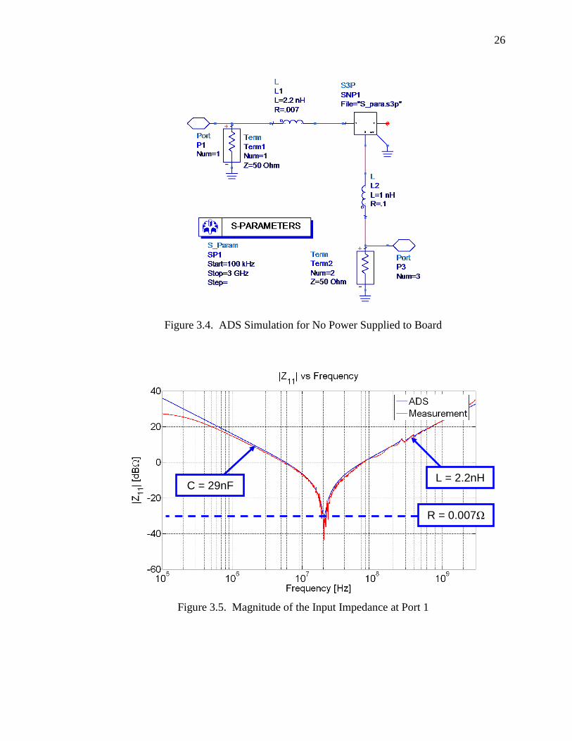
Figure 3.4. ADS Simulation for No Power Supplied to Board ........................................ 26
Figure 3.5. Magnitude of the Input Impedance at Port 1 ................................................. 26
Figure 3.6. Magnitude of the Transfer Impedance Between Ports 1 and 3 ..................... 27
Figure 3.7. Magnitude of the Input Impedance at Port 3 ................................................. 27
Figure 3.8. ADS Model .................................................................................................... 28
Figure 3.9. Magnitude of Z13 ADS and EzPP Simulation Results vs. Measurements ..... 29
Figure 3.10. Initial Schematic Used for Analytical Calculations .....................................30
Figure 3.11. Simplified Circuit for Z13 Calculations ........................................................31
Figure 3.12. Z13 Magnitude Comparison ..........................................................................32
Figure 3.13. Schematic Including Higher Mode Inductance Used in Analytical
Calculations...................................................................................................33
Figure 3.14. Z13 Magnitude Comparison with Higher Mode Inductance Added into
the Model ......................................................................................................33
Figure 3.15. Schematic Including Higher Mode Inductance and Parallel Resistance ......34
Figure 3.16. Z13 Magnitude Comparison with Higher Mode Inductance and Parallel
Resistance Added into the Model .................................................................34
Figure 3.17. Input Impedance for Port 1 ...........................................................................36
Figure 3.18. Input Impedance Seen at Port 3 ....................................................................36
Figure 3.19. ADS Simulation Results for Port Two Impedances .....................................37
Figure 4.1. Copper Strap .................................................................................................. 40
Figure 4.2. Copper Strap Wrapped in Electrical Tape ..................................................... 40
Figure 4.3. Input Impedance of Current Strap ................................................................. 41
Figure 4.4. Equivalent Circuit Model for Transfer Impedance Measurement Setup ....... 41
Figure 4.5. Current Probe Transfer Impedance Measurement Setup............................... 42
Figure 4.6. Transfer Impedance of the Three Current Probes Tested .............................. 43
Figure 4.7. Manufacture's Transfer Impedance Plot for the F-61 .................................... 43
Figure 4.8. Manufacture's Transfer Impedance Plot for the F-62 .................................... 44
Figure 4.9. Manufacture's Transfer Impedance Plot for the F-65 .................................... 44
Figure 4.10. IGBT Schematic .......................................................................................... 45
Figure 4.11. IGBT Pin and Component Locations .......................................................... 45
Figure 4.12. Probe Connection Across IGBT Shown on the Schematic ......................... 46
Figure 4.13. Probe Connection to IGBT Module ............................................................ 47
Figure 4.14. Setup for Transfer Impedance from IGBT to Cables Leading to the Motor 47
Figure 4.15. Input Impedance Seen from Inside the IGBT.............................................. 48

ix
Figure 4.16. Transfer Impedance from IGBT to Cables ...................................................49
Figure 4.17. Copper Triangle Used to Connect the Center Conductor to the Three
Phases and Reduce Inductance .....................................................................50
Figure 4.18. Copper Tape Was Used for Connection of Outer Conductor of the
Probe to the Heat Sink ..................................................................................51
Figure 4.19. Measurement Setup for the Impedance Measured Outside the IGBT
Module ..........................................................................................................51
Figure 4.20. Transfer Impedance Magnitude Taken Outside of the IGBT Module .........52
Figure 4.21. Transfer Impedance Phase Taken Outside of the IGBT Module ................ 53
Figure 5.1. CST Model Used for Single Layer of Serpentine Coil...................................55
Figure 5.2. CST Model Used for Two Layers of Serpentine Coils ..................................56
Figure 5.3. CST Model Using Two Coil Layers and Larger Vias ....................................57
Figure 5.4. Two Layer Model‟s Magnetic Fields Seen with a Cut Plane Placed in
Model ..............................................................................................................58
Figure 5.5. Two Layer Model‟s Magnetic Fields Seen at an Inch Away from the
Coils ................................................................................................................59
Figure 5.6. One Layer Model‟s Magnetic Fields Seen from an Inch Away from the
Coils ................................................................................................................59
Figure 5.7. PSPICE Model................................................................................................60
Figure 5.8. PSPICE Results for Two Coils Comparing the Values of C1 and L1
Over Time .......................................................................................................61
Figure 5.9. Comparison for One and Two Layers of Coils ..............................................61
Figure 5.10. Back Side of Manufactured PCB .................................................................62
Figure 5.11. Front Side of Manufactured PCB .................................................................63
Figure 5.12. Change in Model without the Turn of 90 degrees ........................................64
Figure 5.13. Solution to the Electrostatic Discharge Problem from the Power
Connection to the Return Trace ....................................................................64
Figure 5.14. Return Trace Changes ..................................................................................65
Figure 5.15. CST Model Used for Simulation of New Design .........................................66
Figure 5.16. Modified Coils Field Distribution at an Inch Away from Coils with
240 mil Separation Between Coils and Return Plane ...................................66
Figure 5.17. H-field Distribution at an Inch Away from Coils with a Separation of
¾ of an Inch Between Layers .......................................................................67
Figure 5.18. H-field Distribution at an Inch Away from Coils with a Separation of
an Inch Between Layers ................................................................................68
Figure 5.19. Equivalent Circuit .........................................................................................68
Figure 5.20. Current Through Coils vs. Time ...................................................................70

x
Figure 5.21. Current Through Coils vs. Frequency ..........................................................70
Figure 5.22. New PCB Design ..........................................................................................73
Figure 5.23. New Setup ....................................................................................................73

xi
LIST OF TABLES
Page
Table 2.1. Self and Mutual Inductance Results for Phase One ........................................ 11
Table 2.2. Simulation and Measurement Results............................................................. 18
Table 2.3. Q3D Calculated Capacitances in pF ............................................................... 20
Table 3.1. TMz Modes ..................................................................................................... 25

1
1. INTRODUCTION
Today's world is driven by the fastest and smallest electronics. Therefore, the
market is in the hands of the designers who can not only meet these requirements, but
surpass the rest of their competitors at the lowest cost. Many limits face engineers when
designing such a system, such as current, power, and heat dissipation. This thesis digs
into the challenges seen when dealing with high currents and power. It is broke up into
four different sections along with an appendix. However, it focuses in on three major
areas; motor drives, FBGA package parasitics, and high energy delivering coil
development.
Motor drives designed with IGBTs may operate with a switching speed up to
around 30 kHz and support large currents of 200 to 1000 A. Switching speeds at low
frequencies while driving large amounts of current makes these systems not only involve
the drive but the motor and cable as well. A senior design project evolved and three
students attending Missouri Science and Technology worked with four senior design
students at Rose-Hulman Institute of Technology. The project was broke into two teams
where two students from each school worked on characterizing the IGBTs inside the
motor drive, while one student from Missouri Science and Technology and two students
from Rose-Hulman worked with the motor and cables. As a mentor to the students, I
helped them with measurements, simulations, and calculations. The students were
required to include all of their findings in a report for Rockwell Automation. This report
has been added to this thesis as an appendix. Section 2 shows much of the IGBT
modeling and measurements, while the appendix shows some extra parts dealing with the
IGBT and all of the motor and cable documentation. Section 4 deals with a larger motor
drive from the same company having similar problems and was analyzed using the same
setup for the motor and cables. When analyzing devices with large currents, the first step
is to trace all the current paths. The current being transferred from the drive to the cables
becomes the concern. In the process of analyzing these currents, current probes were
used. Characterizing current probes and the effect they have on measurements proved to
be a large part of this project and is also shown in detail in Section 4.

2
Although negligible in previous generations of products, these parasitic elements
become an issue when increasing the speed of operation and decreasing the size. A PCB
with crowded traces on each layer requires designers who optimize the performance of
the device to call upon special tricks and techniques. Operating at frequencies which
impose substantial dispersion on a signal may be corrected by applying pre-emphasis on
the signal. This method involves boosting those frequency components that are
attenuated by the transmission line. Understanding the impedance the signal encounters
as it travels across the board is an important part of this method. Section 3 discusses the
measurements, simulations, and analytical calculations involved when finding these
impedances.
The ability to transfer large amounts of energy between systems has been around
for many years. Although most of these devices are large and bulky, the design analyzed
and constructed in this thesis is all about size, weight, and performance. Section 5
discusses how to achieve large amounts of magnetic fields transferred to other devices
while keeping the coils light weight and small. Dealing with these high currents and
voltages generate other problems which are not as much of a concern when dealing with
low voltage circuits, such as Electrostatic Discharge (ESD). However, the physics
remains the same and is the driving point of this subject just as it is with the other
subjects discussed in this thesis.

3
2. PARASITIC COMPONENTS OF IGBT MODULES
Insulated Gate Bipolar-junction Transistors (IGBT) are used much of the time in
power electronic circuits for motor controls, because they can with stand large currents.
Changing the frequency these IGBTs switch and the amplitude of the input signal allows
the circuit to control the motor. The module's inductance and capacitance was examined
to see what effect it played in the overall impedance of the motor drive, since it was
reported by users that the drive radiated emissions around 30 MHz. The IGBT module
studied was used in a three phase motor drive and is shown in Figure 2.1. To eliminate
confusion and keep organization, the larger copper area fill of the IGBT were assigned a
letter.
Figure 2.1. IGBT Geometry

4
Figure 2.2. IGBT Labeled Area Fills
2.1. INDUCTANCE
Inductance shows up all over the IGBT module expressing itself as self and
mutual inductance. For a complete circuit model of the IGBT module, both of these must
be examined. Self inductance is defined in equation 1 as the ratio of the magnetic flux
linkage to the current flowing through the geometry. The magnetic flux linkage for one
loop is expressed in equation 2
L =Φ
I (1)
Φ = B ∙ ds
S (2)
Current paths are the sole key to finding the parasitic inductances buried in this
module. Therefore, each possible path had to be traced and shown in Figure 2.3. The
actual value for the total inductance of each path is obtainable only by measurements, but
would prove to be difficult when trying to split up all of the self and mutual inductances
of the module. Therefore, simulations were also performed. Each path was modeled in a
full-wave simulation tool, and the simulation results were compared to measured results.
Once these results matched, the model was able to be broke apart to find self and mutual
inductances of the bond wires and area fills. The calculated inductance values gained
from simulating parts of the model were used to create an equivalent circuit model.

5
Figure 2.3. Current Paths for All Three Phases
2.1.1. Inductance Measurements. The first path analyzed was phase one whose
current path is shown in Figure 2.4. The measurement was performed using a semi-rigid
coaxial probe. The outer shield of the coax was soldered to the heat sink, and the center
conductor was soldered to the location where the DC rail connected to area fill A from
pin 22. This was the input of the intended current path of phase one. Bond wires that
were not part of this phase leg were removed. Where the intentional current path of
phase one would exit to the motor through bond wires from area fill I to pin six, a strap of
copper tape was used to short area fill I to the heat sink as shown in Figure 2.5. The
measurement was taken with a Vector Network Analyzer (VNA) to obtain scattering
parameters. The impedance for this path was found by using equation 3.
Z11 = Z0 1+S11
1−S11 (3)

6
Figure 2.4. Current Path of Phase 1
Figure 2.5. Measurement Setup for Phase One
2.1.2. Inductance Simulations. Simulations were performed to validate the
measurements. These simulations were completed using the two full-wave modeling
tools CST Microwave Studio and Ansoft's Q3D. While Microwave Studio calculates the
field distributions and the impedance associated with the module, Q3D calculates the
inductance, resistance, and capacitance matrices needed to generate a SPICE model. The
Microwave Studio and Q3D model created is shown in Figure 2.6.

7
Figure 2.6. Simulation Model for Phase One
The model contained both the short on area fill I and the probe wire on area fill A.
The short was placed on area fill I, because this is where the current left the IGBT. To
setup the simulation in Q3D, a source was added to the bottom of the probe wire and the
sink was place below it. The placement of the port was based on the way the
measurements were performed. The calibration plane of the VNA was at the point where
the outer shield of the probe was stripped and the center conductor was left exposed.
For the CST Microwave Studio model, a discrete port was placed between the
center of the probe wire and the heat sink. Microwave Studio calculated the input
impedance of the loop which was compared to the measurements. This comparison is
shown in Figure 2.7. From the input impedance, the total inductance of phase one can be
found. The slope of the input impedance magnitude at low frequencies in Figure 2.8 is
20 dB per decade and the phase is negative 90 degrees. These are classic characteristics
of an inductor. Therefore, we can find the total inductance of phase one using equation 4.
Zin = jωL (4)

8
Figure 2.7. Phase One Impedance Comparison
The measurement for the total inductance was performed relatively smooth, but
measurements for each individual inductance in the phase would prove to be
complicated. However, taking advantage of numerical modeling would create a window
of opportunity when facing this obstacle. The phase leg was split into many sections.
Each area fill, group of bond wires, and probe wire was simulated separately. Figure 2.8
shows the labeling for the different sections simulated. The inductance values were
pulled from these simulations and place into the ADS model shown in Figure 2.9. The
simulation results from the equivalent circuit model are shown in Figure 2.10.

9
Figure 2.8. Labeled Sections of Simulation Model
Figure 2.9. Phase One ADS M2 Model
Figure 2.10. Phase One ADS M2 Model Results
L probe C afA ,L afA
L b1
C afG L afG
L b2
C afA ,L afA
L probe C afA ,L afA
L b1
C afG L afG
L b2
C afI ,L afI

10
As the plots show, the CST and ADS simulation results are starting to match up
relatively close. However, the ADS model is still missing the mutual inductances which
are difficult to find using Microwave Studio. As shown before, Microwave Studio can be
used to find the self inductances of a structure, yet when it comes to finding mutual
inductances other simulation programs should be used.
To find the mutual inductance, Ansoft's tool Q3D was used. Q3D was used find
the unknown mutual inductances as well as check some of the previous Microwave
Studio results. To calculate the mutual inductances, the current path was broken apart.
For the probe, the geometry is shown in Figure 2.11. The source was assigned to the
circular face at the start of the probe wire, while the other end of the probe wire
connected to a block which acted as a short to the heat sink. The sink consisted of a
circular sheet positioned on the heat sink directly below the source.
Figure 2.11. Q3D Model Used to Calculate the Inductance of the Probe
A similar simulation was created for the two bond wires connecting area fill A
and area fill G. A source was placed at the start of each bond wire and a short was placed
at the end of the bond wires. A sink was placed below the bond wires by placing a
rectangular sheet on top of the heat sink. Figure 2.12 shows this model. For the four
bond wires between area fill G and area fill I, a simulation like the previous simulations
was created. Figure 2.13 shows this model. These simulations calculated the self and
mutual inductance associated with the bond wires, and the values are recorded in Table
2.1.

11
Figure 2.12. Q3D Model Used to Calculate the Inductance of Two Bond Wires
Figure 2.13. Q3D Model Used to Calculate the Inductance of Four Bond Wires
Table 2.1. Self and Mutual Inductance Results for Phase One
Bond
Wire Probe 1 2 3 4 5 6
Probe 2.4681 - - - - - -
1 - 4.6245 1.9832 - - - -
2 - 1.8932 4.6559 - - - -
3 - - - 2.9482 0.99674 0.25004 0.13747
4 - - - 0.99674 2.9094 0.4542 0.2552
5 - - - 0.25004 0.4542 2.9131 1.0001
6 - - - 0.13747 0.2552 1.0001 2.9496
12
The next step was to find the self inductance of each area fill. These inductances
were found the same way. The source was placed on top of the area fill where the probe
wire connected. The short was on the other end where the bond wires left the area fill.
The sink was placed below the source on top of the heat sink as portrayed in Figure 2.14.
Figure 2.14. Q3D Model for Self Inductance Calculation of Area Fill A
The other area fills were calculated using the same procedure. The method for
building these simulations included putting the source where the current enters the area
fill, a short where the current leaves the area fill, and the sink where the current path
returns to the source.
After these values were found, they were all entered it the ADS model shown in
Figure 2.15. The results of the new ADS model compared to the measured data are
shown in Figure 2.16.

13
Figure 2.15. ADS Model Using Q3D Calculated Values
Figure 2.16. Comparison of ADS Results and Measured Values

14
2.2. CAPACITANCE
2.2.1. Capacitance Measurements. The three capacitances for the IGBT
modules are the junction capacitance, plate to plate capacitance, and the plate to reference
capacitance. The junction capacitance was neglected, because its size is relatively
smaller than that of the plate to reference and plate to plate capacitance. Therefore, the
two examined were the plate to plate and plate to reference. Measurements would also
have to be performed on the substrate to find the dielectric constant. This is a
fundamental element in obtaining accurate simulations which could be compared to the
measurements. After finding the dielectric constant, it would be entered into the full-
wave simulation tool.
In order to find the dielectric constant, the components and copper area fills were
removed from a piece of the substrate on the module using a Dremel tool. The substrate
was then removed from the modules heat sink by heating the heat sink on a hot plate and
lifting the substrate off. After the substrate was cleaned off and removed from the
module, copper was sputtered on it. A utility knife was used to scratch the copper off of
the edges, so the edges did not contain a short from the top plane to the bottom plane.
This measurement was performed by using a semi-ridged coaxial probe where the center
conductor was connected to one side, and the outer conductor was connected to the other
side by soldering a copper strap from the outer conductor to the copper plane as shown in
Figure 2.17 and Figure 2.18. The measurements are portrayed in Figure 2.19.
Figure 2.17. Substrate Capacitance Measurement Setup for Center Conductor
Connection

15
Figure 2.18. Substrate Capacitance Measurement Setup for Outer Conductor Connection
Figure 2.19. Substrate Capacitance Measurement Results
By knowing the capacitance, the value for the relative permittivity can be found.
The area of the copper sputtered substrate was calculated to be 672.5 µm2 by using the
dimensions shown in Figure 2.20. The thickness of the substrate was measured to be
0.392 mm. The capacitance measured with the Impedance Analyzer was 162.7 pF.
Therefore, the relative Permittivity was calculated using equation 5 to be 10.7. Where A
is the area of the plane, d is the distance between the two planes, ε0 is the permittivity,
and εr is the relative permittivity or dielectric constant.
C = 162.7 pF

16
Figure 2.20. Substrate Dimensions
εA
d=
ε0εr A
d (5)
The calculated value of εr is close yet was not easily found, since the thickness of
the substrate was hard to measure. Because the dielectric constant depends greatly on the
thickness, the simulation values may contain error.
Measuring the plate to reference capacitance required removing all the bond wires
connected to the area fill, so all that was left was the area fill of copper above the heat
sink as shown in Figure 2.21.
Figure 2.21. The Bond Wires were Removed from the IGBT Module to Measure the
Capacitance of the Major Area Fills

17
The measurement setup consisted of the outer shield of a coaxial probe soldered
to the heat sink and the center conductor soldered to the copper area fill. The setup is
shown below in Figure 2.22, and the impedance measured using the Impedance Analyzer
is shown in Figure 2.23.
Figure 2.22. Measurement Setup for Area Fill B Capacitance
Figure 2.23. Measurement Results for Area Fill B Impedance
C = 37.3 pF

18
Measurements were performed on area fills A, B, G, and I. These measurements
were also performed using a LCR meter for comparison. For the LCR measurements,
one terminal was clipped to the heat sink, while the other terminal was used to touch each
area fill directly. The measured capacitance values for the area fills found by the
Impedance Analyzer and LCR meter are shown in Table 2.2.
2.2.2. Capacitance Simulations. Capacitance simulations were performed using
both CST and Q3D. CST models were created neglecting the plate to plate and only
considered the plate to reference capacitance for each area fill. Figure 2.24 shows the
CST model for area fill B and Figure 2.25 shows the results of the simulation. The
effects of these adjacent area fills were examined using Q3D. Simulations were
generated for each area fill in phase one. These values are shown in Table 2.2.
Table 2.2. Simulation and Measurement Results
CST Impedance
Analyzer
LCR
Meter
Area A 35.4 pF 33.4 pF -
Area B 40.0 pF 37.3 pF 38 pF
Area G 58.7 pF 52.8 pF 53 pF
Area I 45.4 pF 39.6 pF 41 pF
19
Figure 2.24. CST Model for Area Fill B
Figure 2.25. CST Simulation Results for the Input Impedance at Port One
The values calculated by CST were used in the ADS model shown in Figure 2.9
and the impedance plot of the ADS and CST simulations are compared in Figure 2.10.
Ansoft‟s Q3D was used to compare with the capacitance simulations generated by CST.
When using Q3D to solely find the capacitance and nothing else, there are no sources or
Calculated C: 40.0 pF

20
sinks incorporated in the simulation. Each area fill along with the heat sink was put into
their individual net, and the simulation was then setup to find only capacitance. The
model is shown in Figure 2.26 and included area fill A, G, and I. Unlike CST, Q3D finds
the self and mutual capacitance values and places those values into a matrix. The
calculated capacitances are shown in Table 2.3.
Figure 2.26. Q3D Capacitance Simulation Model
Table 2.3. Q3D Calculated Capacitances in pF
Area Fill A Area Fill G Area Fill I Heat
sink
Area Fill A - 0.00578 0.00147 31.88
Area Fill G 0.005799 - 0.007563 54.031
Area Fill I 0.00147 0.007563 - 39.581
Heat Sink 31.88 54.031 39.581 -

21
3. FBGA PARASITIC INDUCTANCES
The Altera Stratix II FineLine Ball-Grid Array (FBGA), along with their program
Quartus, can be used together to predict the impedance across the board and add pre-
emphasis to the signal leaving the FBGA package. This increases the signal‟s integrity to
the point where it can be read accurately anywhere across the board. Measurements and
simulations were made to see the influence the chip had on the impedances seen across
the board. The measurements setup for the test board which was analyzed is shown in
Figure 3.1, and the dimensions of the board are shown in Figure 3.2. Port 1 was a
standard SMA jack, port 2 was an imaginary port placed at the center of the FBGA, and
port 3 consisted of a semi-rigid coaxial probe. The outer conductor of the probe was
soldered to a surface mount capacitor GND pad, and the center conductor was soldered to
the VCCL pad. To find the different impedances seen from port 2 to other areas on the
board, ports 1 and 3 were analyzed, since port 2 was inside the FBGA making
measurements difficult. Calculations were performed showing that the transfer
impedance between port one and three includes all the components that are in the transfer
impedances of port two as well as the input impedance. Therefore, having the correct
equivalent circuit model for Z13, one can find the impedances seen at port two using the
same model.

22
Figure 3.1. Geometry of FBGA Test Board
Figure 3.2. Dimensions and Placement for Measurements and Simulations
Port 3 Coaxial Probe
Port 1 SMA Jack
Port 2 FBGA
Power Cables

23
3.1. IMPEDANCES SEEN AT PORTS ONE AND THREE
3.1.1. Measurements. Scattering parameter measurements were taken at port 1
and 3 using a Vector Network Analyzer and were later converted to Z-parameters.
Measurements were made on the board shown in Figure 3.1 which had no capacitors.
The VNA was calibrated at port 1 to the tip of the probe where the center conductor was
no longer shielded by the outer conductor. Port 3 was calibrated up to the point where
the center conductor extrudes out of the SMA jack. Measurements were carried out with
the FBGA powered on and off to see how the impedance changed. With no power
hooked to the FBGA, the total capacitance of 29 nF was due to the capacitance of the
board alone. When the FBGA was powered on, the total capacitance increased to 460 nF
and was due to the capacitance of the board and FBGA. Therefore, the capacitance of the
FBGA when the board is powered on is 431 nF.
3.1.2. Simulations. To match the measurement results, two types of simulations
were performed. One simulation dealt with circuit components, and the other dealt with
the parallel plane behavior. ADS was originally used to simulate the circuit components,
but then the equations were derived and placed into Matlab. The program Ez-Power
Plane (EzPP) was used to simulate the parallel power and return planes effect seen on the
board. EzPP requires dimensions which are found in the stack-up of the board shown in
Figure 3.3. This figure illustrates the separation of the planes, the placement of the
circuit components used for the package, and the pieces added by Ez-Power Plane.

24
Figure 3.3. Altera Stratix II PCB Stack-Up
The program Ez-Power Plane (EzPP), created by the University of Missouri-Rolla
Electromagnetic Compatibility Laboratory, was used to find the portion of the curve
accountable for the wave propagations between the power and ground layers. This
program looks at the low frequency parallel plate capacitance which is the capacitance
added by the power and ground planes. It also takes into account the higher mode
inductance and the resonance frequencies associated with the port locations and
dimensions which are portrayed in Figure 3.2. Three ports were used in the EzPP
simulation. The two ports used in the measurements were placed inside the EzPP
simulation as well as a port placed at the center of the chip. The x-y port locations can be
seen in Figure 3.2. The port size used for these simulations was a square 0.6 mm by 0.6
mm port. This value was the radius of the of the balls of the FBGA and was pulled from
the Altera datasheet of the Stratix II. The dielectric thickness was set to four mils and the
dielectric constant was set to 4.3. The loss tangent was set to 0.02. The metal thickness
was 0.7 mils with a conductivity of copper.
In this case, the distributed portion is dominated by the geometry of the board.
The first resonance for a board which is 10 inches by 10.5 inches is the TMz10 mode at
276 MHz. This frequency along with the other modes can be found by equation 6 and a
few of these modes were calculated and are shown in Table 3.1
25
fc m, n =1
2π μϵ
mπ
a
2
+ nπ
b
2
a > 𝑏, 𝑚 > 0 , 𝑛 > 0 (6)
Table 3.1. TMz Modes
TMz Modes
b=10 in a=10.5 in n = 0 n = 1 n = 2 n = 3 n = 4
m = 0 - 2.89E+08 5.78E+08 8.67E+08 1.16E+09
m = 1 2.76E+08 4.00E+08 6.41E+08 9.10E+08 1.19E+09
m = 2 5.52E+08 6.23E+08 7.99E+08 1.03E+09 1.28E+09
m = 3 8.28E+08 8.77E+08 1.01E+09 1.20E+09 1.42E+09
m = 4 1.10E+09 1.14E+09 1.25E+09 1.40E+09 1.60E+09
Everything below the TMz10 mode may be modeled using passive circuit
components. The ADS model for the board when there is no power supplied is shown in
Figure 3.4. The block labeled SNP1 stores the touchstone file created by EzPP, which
implements the influence the planes have on the circuit. There are no connections
attached to port 2 in this simulation, since no power was supplied to the FBGA. The two
capacitances were found from the measurements to be 431 nF for the FBGA and 29 nF
for the printed circuit board. The inductances and resistances were found from the
measurements looking at the input impedances of ports one and three. Figures 3.5 and
3.7 show the input impedances of ports 1 and 3, and Figure 3.6 shows the transfer
impedance between the two ports. These measurement and simulation comparisons were
primarily to check that the model is correct before analyzing the FBGA effects on the
board impedance.
26
Figure 3.4. ADS Simulation for No Power Supplied to Board
Figure 3.5. Magnitude of the Input Impedance at Port 1
C = 29nF L = 2.2nH
R = 0.007Ω

27
Figure 3.6. Magnitude of the Transfer Impedance Between Ports 1 and 3
Figure 3.7. Magnitude of the Input Impedance at Port 3
C = 29nF
28
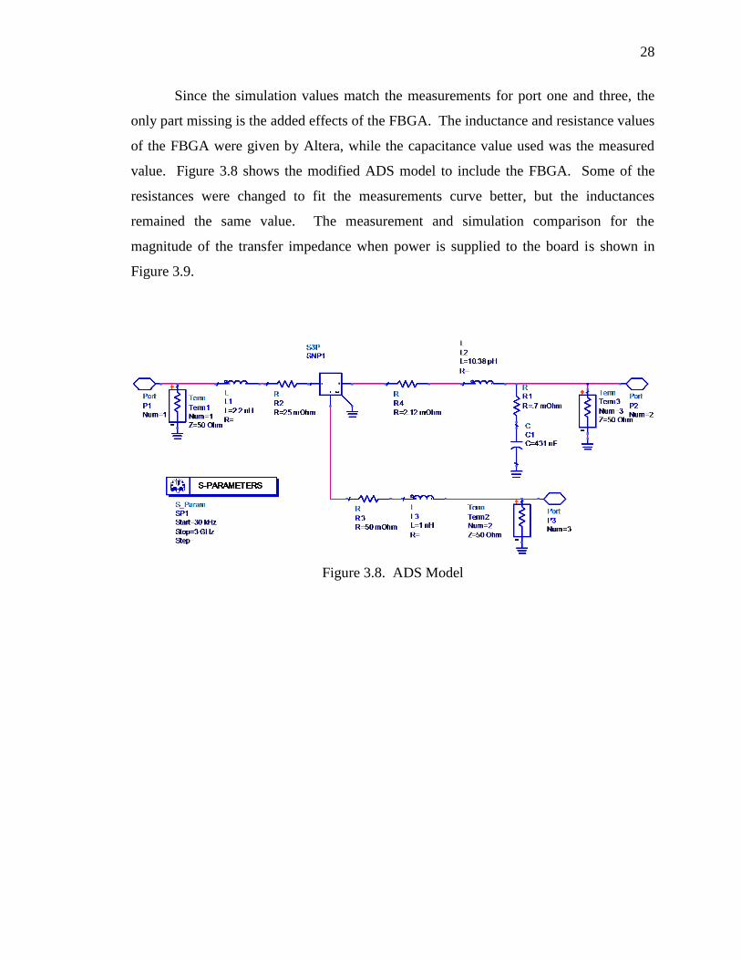
Since the simulation values match the measurements for port one and three, the
only part missing is the added effects of the FBGA. The inductance and resistance values
of the FBGA were given by Altera, while the capacitance value used was the measured
value. Figure 3.8 shows the modified ADS model to include the FBGA. Some of the
resistances were changed to fit the measurements curve better, but the inductances
remained the same value. The measurement and simulation comparison for the
magnitude of the transfer impedance when power is supplied to the board is shown in
Figure 3.9.
Figure 3.8. ADS Model
29
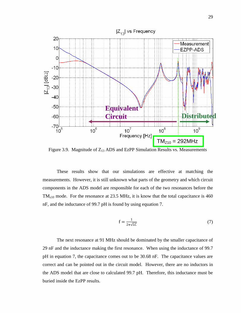
Figure 3.9. Magnitude of Z13 ADS and EzPP Simulation Results vs. Measurements
These results show that our simulations are effective at matching the
measurements. However, it is still unknown what parts of the geometry and which circuit
components in the ADS model are responsible for each of the two resonances before the
TMz10 mode. For the resonance at 23.5 MHz, it is know that the total capacitance is 460
nF, and the inductance of 99.7 pH is found by using equation 7.
f =1
2π LC (7)
The next resonance at 91 MHz should be dominated by the smaller capacitance of
29 nF and the inductance making the first resonance. When using the inductance of 99.7
pH in equation 7, the capacitance comes out to be 30.68 nF. The capacitance values are
correct and can be pointed out in the circuit model. However, there are no inductors in
the ADS model that are close to calculated 99.7 pH. Therefore, this inductance must be
buried inside the EzPP results.
Equivalent
Circuit Distributed
TMZ10 = 292MHz

30
3.1.3. Analytical Calculations. Calculations were made by hand and then
entered into Matlab to compare the analytical calculations with the measurements and
simulations. The initial schematic shown in Figure 3.10 is similar to the ADS model in
Figure 3.8 except the s-parameter box that include the touchstone file generated by EzPP
was replaced with a capacitor Cplanes which represented the capacitance of the planes. R
is the added resistance of the planes between ports. Lport and Rport are the measured
inductance and resistance of port one. Similarly, Lprobe and Rprobe are the measured
inductance and resistance of port three. Ltotal includes all the inductances add to the
circuit by the internal inductance of the package and package connection seen in Figure
3.3. This value was given by Altera to be their measured inductance. Rpkg and Cpkg was
the resistance and capacitance introduced to the circuit by the chip. Rpkg was given by
Altera as their measured inductance, and Cpkg was the measured capacitance of the
package which is shown in Figures 3.5, 3.6, and 3.7.
Figure 3.10. Initial Schematic Used for Analytical Calculations
Cplanes
Cpkg
Cpkg = 431 nF

31
The transfer impedance was derived using the definition of the transfer impedance
from port one to three which is given by equation 8. It says the transfer impedance from
port one to port three is defined as the voltage seen at port one divided by the current seen
at port three while the current at all other ports are set to zero. When using equation 8 to
find Z13, the circuit shown in Figure 3.10 simplifies to the circuit shown in Figure 3.11.
The calculations are shown in equations 9 and 10.
Z13 = V1
I3 I1=0
I2=0
(8)
Figure 3.11. Simplified Circuit for Z13 Calculations
Z13 =
1
sCplane sLtotal +R+Rpkg +
1
sCpkg
1
s Cplane+sLtotal +R+Rpkg +
1
sCpkg
(9)
Z13 =Ltotal Cpkg s2+ R+Rpkg Cpkg s+1
s Ltotal Cp lane Cpkg s2+ R+Rpkg Cplane Cpkg s+ Cplane +Cpkg (10)
Note that there are no influences by either the probe at port three or the SMA jack
at port one. Therefore, the impedance of the planes and the FBGA are known once Z13 is
obtained. Equation 10 was entered into Matlab, and the results were compared with the
1V
3I

32
measurements and simulations. As it can be seen below in Figure 3.12, the capacitance
alone does not come close to creating an accurate simplified model of the EzPP block in
the ADS model. While the measurement and ADS model match fairly well, the
analytical calculations of the circuit appear to be missing an inductance. The inductance
needed to hit the first resonance at 23.5 MHz was found earlier to be 99.7 pH. Therefore,
some changes were made to the initial model, so the analytically calculated results match
the ADS model better.
Figure 3.12. Z13 Magnitude Comparison
Making the curves match better was accomplished by adding the inductor Lplanes
with a value of 91 pH to the model, as shown in Figure 3.13. This is the inductance
calculated by EzPP that is associated with the port size and location. The effect of this
inductance is critical, since it shifts the curve onto the measurements and ADS curves as
shown in Figure 3.14.

33
Figure 3.13. Schematic Including Higher Mode Inductance Used in Analytical
Calculations
Figure 3.14. Z13 Magnitude Comparison with Higher Mode Inductance Added into the
Model
Cpkg
Cpkg = 431 nF

34
This model is still not quite right. A resistance is needed to make the second
resonance match. The second resonance is a pole at 91 MHz and is formed by the
capacitor Cplanes, the sum of the inductance of Lplanes and Ltotal, and the added resistance
RG resonating in parallel. Adding the resistance RG in parallel with the capacitance in
Figure 3.15 made the curve matched much better as shown in Figure 3.16.
Figure 3.15. Schematic Including Higher Mode Inductance and Parallel Resistance
Figure 3.16. Z13 Magnitude Comparison with Higher Mode Inductance and Parallel
Resistance Added into the Model
Cpkg
Cpkg = 431 nF

35
The three curves match up to the second resonance which covers the lumped
element part of the circuit. The third resonance is the TMz10 mode and draws the line
between the equivalent circuit part of the impedance plot and the distributed part as
shown earlier in Figure 3.9.
After the transfer impedance plot was sound, the input impedance at port one and
three needed to be checked. The input impedances at the ports were derived starting with
their definitions. Equation 11 shows the definition for the input impedance at port one,
and equation 12 shows the equation for port three.
Z11 = V1
I1 I2=0
I3=0
(11)
Z33 = V3
I3 I1=0
I2=0
(12)
Deriving the input impedance at port one and three involved little effort, since the
impedance for everything else other than resistance and inductance of the port or probe
was incorporated into the transfer impedance equation. For this reason, the transfer
impedance is found in the input impedance equations for port one and three. The derived
equation for Z11 can be seen in equation 13 and Z33 can be seen in equation 14.
Z11 =50 Lport s+Rport +Z13
50+Lport s+Rport +Z13 (13)
Z33 =50 Lprobe s+Rprobe +Z13
50+Lprobe s+Rprobe +Z13 (14)
Figures 3.17 and 3.18 show the comparison between the plots of the analytical
equations entered into Matlab and the simulation and measurement results. It should be
noted that the port inductance seen in EzPP plays a huge role in the resonance around 91
MHz. This resonance would not be seen at all if the inductance Lplanes was removed from
the circuit.

36
Figure 3.17. Input Impedance for Port 1
Figure 3.18. Input Impedance Seen at Port 3
91 MHz
91 MHz

37
3.2. IMPEDANCES SEEN AT PORT TWO
Since the measurements were too difficult to make, only simulations and
analytical calculations were performed for port two.
3.2.1. Simulations. Using the same ADS model shown in Figure 3.8, the transfer
impedances Z12 and Z32 along with the input impedance Z22 were simulated and the
results are illustrated in Figure 3.19. All three of the curves show an inductance at first.
The first resonance caused by the equivalent circuit model is a pole seen at 91MHz. This
is the same pole that was seen before in Z13. A second resonance is seen in the Z32 which
is a zero around 190 MHz. The rest of these resonances are dominated by the effects seen
by the geometry of the board.
Figure 3.19. ADS Simulation Results for Port Two Impedances
3.2.2. Analytical Calculations. The same analytical calculations were performed
for port two that were completed previously for ports one and three using the schematic
shown in Figure 3.15.

38
The transfer impedance of port one to port two as well as the impedance from port
three to port two was examined. The transfer impedance equations for Z12 and Z32 are
given in equations 15 and 16.
Z12 = V1
I2 I1=0
I3=0
=Rpkg Cpkg s+1
s Ltotal Cplane Cpkg s2+ R+Rpkg Cplane Cpkg s+ Cplane +Cpkg (15)
Z32 = V3
I2 I1=0
I3=0
= R+Rpkg Cpkg s+1
s Ltotal Cplane Cpkg s2+ R+Rpkg Cplane Cpkg s+ Cplane +Cpkg (16)
The input impedance equation was also derived and is given by equation 17. It
should be noted that the impedances seen at port two all have the same denominator.
This means they all have the same poles although the only one really seen is at 91 MHz
as shown in Figure 3.19. The difference between the impedance curves is seen in the
numerator or the zeros.
Z22 = V2
I2 I1=0
I3=0
= Ltotal Cplane s2+RCplane s+1 Rpkg Cpkg s+1
s Ltotal Cplane Cpkg s2+ R+Rpkg Cplane Cpkg s+ Cplane +Cpkg (17)

39
4. LOCATING PARASITIC CIRCUIT ELEMENTS IN MOTOR DRIVES
The motor drive examined was a variable-frequency drive. These drives vary
frequencies of the AC power supply used to power the motor to regulate the rotational
speed of AC motors. In the system studied, the length of the cable connecting the drive
to the motor was constant, as well as the size of the motor. The drive itself was already
designed although ideas for improvement were encouraged. The frequencies of the
system said to have problems were from 30 MHz to 40 MHz though a wider range was
examined.
4.1. CURRENT PROBE EFFECTS ON MEASUREMENTS
A current probe was used in the setup to find the transfer impedance, so the
effects it had on the measurements' accuracy was of high importance. The Fisher F-61,
F-62, and F-65 were a group of three current probes which were compared and examined.
4.1.1. Copper Strap. A copper strap was used in characterizing of the probes
and the through calibration for calibrating out the effects of the current probe when
finding the transfer impedance of the system. When creating this strap, it was important
to get the loop area as small as possible, yet keep it large enough to fit on the clamp on
the current probes. Another factor that was considered was the strap width. The
narrower the strap was made, the higher the inductance would be due to current
crunching. In this case, the width was made 6 cm, since that was the width of the SMA
jack that was used. The creation of this strap included soldering one end of a strip of
copper to the reference of a SMA jack, and the other end to the center conductor of the
same jack as shown in Figure 4.1. The end soldered to the center conductor was cut to
more of a point where it connected to the jack. This was to help with the connection
mechanically, but to also help eliminate the chance of current crunching which would add
inductance. The copper strap was wrapped in electrical tape after all the connections
were made. This was done to reduce any chances of the strap shorting on the current
probe. Figure 4.2 illustrates this step.

40
Figure 4.1. Copper Strap
Figure 4.2. Copper Strap Wrapped in Electrical Tape
Input impedance measurements were performed on the strap to see how good it
performed at higher frequencies. Figure 4.3 illustrates that the input impedance
magnitude consists of a 20 dB per decade slope and the phase is a relatively firm 90
degrees up to around 300 MHz. At this point, the strap has a real term which begins to
influence the curve, causing the input impedance of the strap to no longer be purely
imaginary. This shows that the calibration becomes a factor of error above 300 MHz.

41
Figure 4.3. Input Impedance of Current Strap
4.1.2. Current Probe Transfer Impedance. The transfer impedance of each
current probe was found using the copper strap created. Since the VNA measures the
voltages at both the current probe and the copper strap, the measurement can be models
as that illustrated in Figure 4.4. The measurement setup for each current probe was the
same and can be seen in Figure 4.5.
Figure 4.4. Equivalent Circuit Model for Transfer Impedance Measurement Setup
106
107
108
109
-20
0
20
40
60
Zin
Magnitude of Current Strap vs Frequency
Frequency[Hz]
Zin
[dB
]Vector Network Analyzer
Impedance Analyzer
106
107
108
109
70
80
90
100
Zin
Phase of Current Strap vs Frequency
Frequency[Hz]
Phase[D
egre
es]
Vector Network Analyzer
Impedance Analyzer
𝑣1+
𝑣2− 𝑣1
−
𝑣2+
Z=50Ω 50Ω
Copper
Strap Z=50Ω
VNA
Port 1
Current
Probe
VNA
Port 2

42
Looking at this model, the transfer impedance was derived by starting with the
fundamental equation. Equation 18 defines the transfer impedance from port one to port
two.
ZT = V1
I2
I1=0=
S21
1−S11Zo (18)
Figure 4.5. Current Probe Transfer Impedance Measurement Setup
After the measurements were taken, the transfer impedance was found using
equation 18. The results of the different probe transfer impedances are shown in Figure
4.6 and can be compared with the manufactures data shown below the measured data in
Figures 4.7, 4.8, and 4.9. However, since the copper strap was used in these
measurements the errors seen before in Figure 4.3 are seen again here once the curve gets
above 300 MHz. Up to this point, the curves for the probes match quite well.
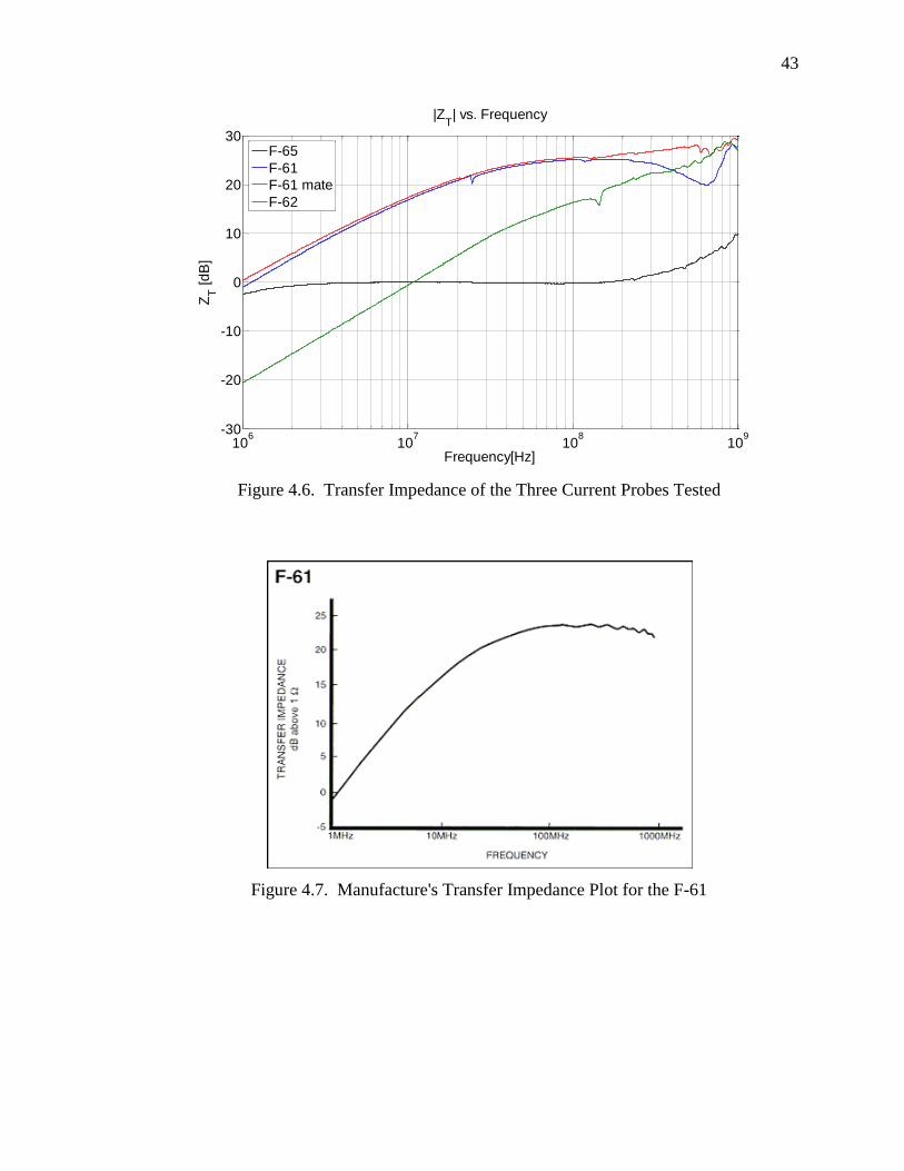
43
Figure 4.6. Transfer Impedance of the Three Current Probes Tested
Figure 4.7. Manufacture's Transfer Impedance Plot for the F-61
106
107
108
109
-30
-20
-10
0
10
20
30
Frequency[Hz]
ZT [d
B]
|ZT| vs. Frequency
F-65
F-61
F-61 mate
F-62

44
Figure 4.8. Manufacture's Transfer Impedance Plot for the F-62
Figure 4.9. Manufacture's Transfer Impedance Plot for the F-65
4.2. MEASURED IMPEDANCE OF MOTOR DRIVE TO CABLES
Measurements began by looking at the source of the switching which was the
IGBT module. One set of measurements was performed by placing a probe inside the
IGBT module, while another set was performed outside of the module. This would show
the effect the module had on the transfer impedance.

45
4.2.1. Measurements Performed from Inside IGBT. The setup for the
measurements started by figuring out where to solder the semi-rigid coaxial probe. The
schematic of the IGBT is shown in Figure 4.10. Figure 4.11 shows the pin and
component locations.
Figure 4.10. IGBT Schematic
Figure 4.11. IGBT Pin and Component Locations
To make this measurement, a semi-rigid coaxial probe was placed across the
collector and emitter of the IGBT with its gate connected to pin 1. The outer conductor

46
was soldered to the collector which was the positive rail. The inner conductor was
connected to the emitter which heads out to the motor. Figures 4.12 and 4.13 illustrate
the connection of the probe. The IGBT is thought of as a source for this measurement,
since it allows the current flow through freely when it switches. Therefore, this
measurement displays what the current sees when the IGBT lets current pass. The
connection of the semi-rigid coaxial probe made up port one. The other port of the VNA
was connected to a current probe clamped around a bus of three wires running from the
drive to the three phase motor. The wires were tied together and spaced 10 inches above
a sheet of aluminum using blue insulating foam to maintain a consistent separation. The
current probe was separated from the cable mounting plate of the drive by five
centimeters. Copper tape was used to create a good path for the current to return from the
aluminum sheet to the heat sink where the reference of the IGBT module was mounted.
The setup is portrayed in Figure 4.14.
Figure 4.12. Probe Connection Across IGBT Shown on the Schematic

47
Figure 4.13. Probe Connection to IGBT Module
Figure 4.14. Setup for Transfer Impedance from IGBT to Cables Leading to the Motor

48
4.2.2. Input Impedance Looking into the IGBT Module. The input impedance
looking into the IGBT module was measured with the impedance analyzer using the low
impedance test head. The setup resembled that shown in Figure 4.14, except the current
probe was not attached. The impedance analyzer was connected to the semi-rigid coaxial
probe. The calibration was performed at the low impedance test head, and a port
extension was used to move the calibration plane up to the tip of the semi-rigid coaxial
probe inside the IGBT. The data taken is shown below in Figure 4.15. Although the
problems were said to be around 30 to 40 MHz, the resonance of the system is centered
around 12 MHz.
Figure 4.15. Input Impedance Seen from Inside the IGBT
4.2.3. IGBT Module to Cable Transfer Impedance. The transfer impedance
between the cable and the IGBT was measured using the Fisher F-61 and F-65 current
probes and a Vector Network Analyzer. The setup for this measurement is illustrated in
Figure 4.14. To remove the effects of the current probe, the through calibration
connection was setup the exactly the same as the measurements setup shown in Figure
4.5. Since the copper strap was used in the calibration, the band of frequencies which the

49
data could be trusted without the error from the copper strap being present included
everything below 300 MHz. The plot of the measured transfer impedance is Figure 4.16.
Below 300 MHz, the curves for the F-61 and its mate were nearly identical. However,
when the curves passed the 300 MHz frequency, they start to vary more as seen
previously when characterizing and testing the current probes. It can be seen from this
plot that the transfer impedance is small around the 30 to 40 MHz range as expected.
Figure 4.16. Transfer Impedance from IGBT to Cables
4.2.4. Transfer Impedance Outside the IGBT Module. Measurements from
were made outside of the IGBT module to see what effects the IGBT module had on the
transfer impedance. By tracing the current paths that leave the module and head to the
motor, the ideal placement of the probe can be found at or just past pins 21 to 29. A
triangular piece of copper was cut and soldered to the connection of the resistors just
outside of the module. At this location, one of the legs of the triangle connected to all
three phases on the board where the current left the IGBT and headed to the motor. The
center conductor of a semi-rigid coaxial probe was soldered to the point of the triangle on
the opposite side of the connection to the board as illustrated by Figure 4.17. The shape

50
of a triangle was used, because it more or less funnels the current into the desired
location. Working at keeping the current from being forced from a wide path to a narrow
path or vice versa minimizes any added inductance.
After the probe and triangle were connected, the board was attached back to the
heat sink and the rest of the structure. The outer conductor of semi-rigid coaxial probe
was connected to the reference of the system by attaching it to the heat sink using copper
tape as shown in Figure 4.18. The full setup was completed and is shown in Figure 4.19.
Figure 4.17. Copper Triangle Used to Connect the Center Conductor to the Three Phases
and Reduce Inductance

51
Figure 4.18. Copper Tape Was Used for Connection of Outer Conductor of the Probe to
the Heat Sink
Figure 4.19. Measurement Setup for the Impedance Measured Outside the IGBT Module

52
The transfer impedance was measured using a Vector Network Analyzer, and the
measurements are shown below in Figures 4.20 and 4.21. Figure 4.20 shows the
magnitude of the transfer impedance where one zero can be seen close to 28 MHz and
another close to 43 MHz. The impedance is allowed to go much higher outside of the
IGBT module, since the capacitance added by the module is not playing a part in the
measurements.
Figure 4.20. Transfer Impedance Magnitude Taken Outside of the IGBT Module
28 MHz 43 MHz
53
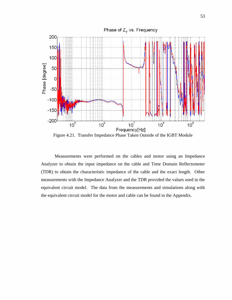
Figure 4.21. Transfer Impedance Phase Taken Outside of the IGBT Module
Measurements were performed on the cables and motor using an Impedance
Analyzer to obtain the input impedance on the cable and Time Domain Reflectometer
(TDR) to obtain the characteristic impedance of the cable and the exact length. Other
measurements with the Impedance Analyzer and the TDR provided the values used in the
equivalent circuit model. The data from the measurements and simulations along with
the equivalent circuit model for the motor and cable can be found in the Appendix.

54
5. ENERGY DELIVERING SYSTEMS
The old saying of how a chain is only as strong as its weakest link also applies to
electronic devices. When disrupting a device, the focus is finding where the weak point
is in the circuit. All components used in circuits have voltage and current ratings, which
is what this energy delivering system attempts to exceed. For most of the cases, the
component which is being pushed past the limit is the microcontroller. Rather it be
destroying the microcontroller or causing it to go into latch-up, the energy delivering
system uses coils to focus strong magnetic fields in specific locations on the device to
guarantee these limits are surpassed inducing large voltages and currents inside the
device. Achieving a maximum emf induced into a victim circuit requires maximizing the
B field of radiated by the culprit. Equation 19 explicates that if the magnetic flux density,
B, is increased the emf will also be increased. The location of the maximum magnetic H
field can also be found by using full-wave simulation tools. Since B is directly
proportional to H as shown in equation 20, the maximum B locations will also be known.
The B field applied to the victim is dependent on time and space. Therefore, the applied
fields generated by the coils can be represented like that shown in equation 21.
emf = E
C∙ dl = −
d
dt B
S∙ ds (19)
B = μH (20)
Ba = ia t fa r (21)
Finding the current applied, ia(t), requires SPICE simulations. The field applied as a
function of space, fa(r), is found from the full-wave simulations.

55
5.1. PROTOTYPE
5.1.1. Simulations. Full-wave simulations were performed using the program
CST Microwave Studio. The original serpentine coil was simulated with zero thickness
to decrease the simulation time. The inductance associated with the thickness of the coil
was considered negligible, since the main interested was finding the inductance
associated with the loop formed by the coil array and the return. The model simulated
can be seen in Figure 5.1.
Figure 5.1. CST Model Used for Single Layer of Serpentine Coil
The bottom layer of the model was a reflector plane. The idea for this plane was
to reflect the fields away from the device as well as shield the device. The plane was set
one inch below the next layer which was the return plane. The return plane was in the
shape of an X in order to keep the geometry symmetric. The length of each crisscross
component was 65 millimeters from the center of the PCB to the end of the component.
The 15 millimeters circular plane located 20 mils above the crisscross return plane was
the power plane. 20 mils above the power layer was the serpentine coils with a trace

56
width of five millimeters. Vias with a diameter of 2 millimeters were used to connect the
coil to the return and the power layers. After a time domain simulation was completed,
the inductance was pulled from the input impedance curve of the coils 45.81 nH.
With some manipulation of Maxwell‟s Equations, it can be shown that the B field
increases with the increase of current through the coils. Another layer of serpentine coils
was placed above the first set of coils, because of the physics behind a solenoid and
knowing that a PCB can have many layers. The vias that were used in the previous
model were extended up to the second coil. This configuration made all eight coils in
parallel. A part of the new model is shown in Figure 5.2.
Figure 5.2. CST Model Used for Two Layers of Serpentine Coils
Doubling the layers decreased the inductance only a little to 44.42 nH from the
45.81 nH. Therefore, this extra layer makes this model more desirable, since it allows an
increase in the current which increases the magnetic fields. Decreasing the inductance
further was accomplished by increasing the diameter of the vias and making it the same
size as the width of the coil traces. The smaller vias made the inductance of the two layer
model come to 44.42 nH, while the larger vias lowered it to 43.67 nH. The two layer
model now looked like that portrayed in Figure 5.3.

57
Figure 5.3. CST Model Using Two Coil Layers and Larger Vias
Field plots were extracted from CST to get a good feel for how the magnetic
fields looked when the serpentine coil was excited. The magnetic fields seen when a cut
plane is placed vertically through two of the coil‟s centers is shown in Figure 5.4. While
one coil pushed the fields through, the other coil pulls the fields. This is what makes the
serpentine array work better than that of a single loop. The serpentine coil keeps the
inductance low, and the array makes the coils work together to create a stronger field
distribution. It can also be seen from Figure 5.4 that the reflector plane binds the fields to
the area between the coil and the reflector plane. The closer the reflector plane is moved
to the coils, the more restricted the fields become. If the reflector was to be placed on the
back of a 62 mil PCB, it would pinch and lower the strength of the fields.
58
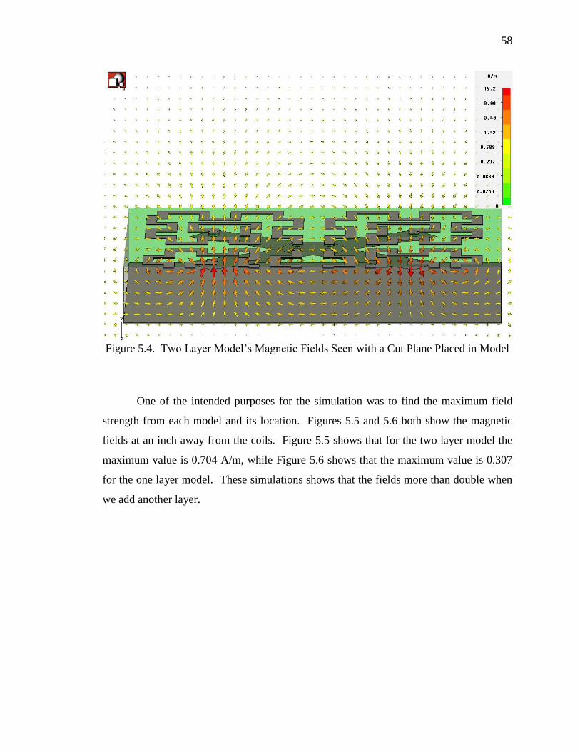
Figure 5.4. Two Layer Model‟s Magnetic Fields Seen with a Cut Plane Placed in Model
One of the intended purposes for the simulation was to find the maximum field
strength from each model and its location. Figures 5.5 and 5.6 both show the magnetic
fields at an inch away from the coils. Figure 5.5 shows that for the two layer model the
maximum value is 0.704 A/m, while Figure 5.6 shows that the maximum value is 0.307
for the one layer model. These simulations shows that the fields more than double when
we add another layer.

59
Figure 5.5. Two Layer Model‟s Magnetic Fields Seen at an Inch Away from the Coils
Figure 5.6. One Layer Model‟s Magnetic Fields Seen from an Inch Away from the Coils

60
After the inductance from the coils had been calculated by CST, they were
inserted into a PSPICE model to find the current through the coil. The design called for
two 34 nF capacitors in parallel which charge up to 40 kV and then discharged across the
coils. The use of one and two 34 nF capacitors was examined for this model. The
inductance of the transmission line was also varied from 10 nH to 100 nH, since the
length of the cable was unsure. In the model shown below in Figure 5.7, the capacitor
bank is C1. The resistance and inductance of the cable is R1 and L1, respectively. L2
was the inductance associated with the coils being pulsed. A switch, U1, has also been
added to make sure PSPICE simulates a capacitor discharging when time is equal zero.
Figure 5.7. PSPICE Model
The current verses time through the two layers of serpentine coils is shown in
Figure 5.8 for the two coils. No matter what size of inductance is introduced by the coil
(43 nH, 44 nH, 50 nH), the current had the same set of curves but with different values.
For both one and two layers of coils, the maximum current was nearly 14.2 kA. For this
simulation, the one circuit element that will make the biggest change in the current is the
resistance in the line, R1. Comparisons were also made between the one layer case and
the two layer case. The difference between these was nearly negligible as shown below
by Figure 5.9. For this figure, the inductances from the larger diameter via simulations
were used.
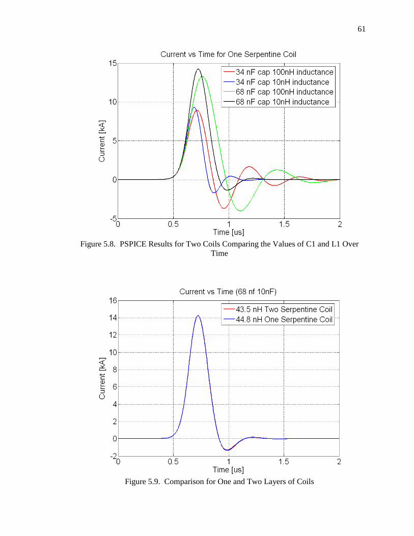
61
Figure 5.8. PSPICE Results for Two Coils Comparing the Values of C1 and L1 Over
Time
Figure 5.9. Comparison for One and Two Layers of Coils

62
5.1.2. Manufacturing the Printed Circuit Board. A PCB was manufactured
after the model had be simulated and performed well. However, the model was changed
when manufacturing the boards. The manufactured board was 62 mils thick and
contained only two layers. The coils were on the top layer and the return was on the
bottom layer. The power layer was more or less moved to the same layer as the coils. It
consisted of a pad with a radius of an inch which covered the start of the coils. A 1/2
inch hole, large enough for the bolt used to attach the power to the coil, was cut out of the
center. Because the power connection was placed in the center, the return had to be
modified. The return became a 300 mil 'U' shaped trace on the bottom of the board. The
return layer contained a hole to bolt the on strap which connects the cable to the coils. A
reflector plane was not part of the board. It could be added later by spacing it with foam
and using copper tape for the plane. The manufactured board is illustrated in Figure 5.10
and 5.11. The bottom layer is Figure 5.10, and the top layer is Figure 5.11.
Figure 5.10. Back Side of Manufactured PCB
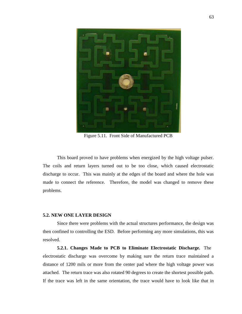
63
Figure 5.11. Front Side of Manufactured PCB
This board proved to have problems when energized by the high voltage pulser.
The coils and return layers turned out to be too close, which caused electrostatic
discharge to occur. This was mainly at the edges of the board and where the hole was
made to connect the reference. Therefore, the model was changed to remove these
problems.
5.2. NEW ONE LAYER DESIGN
Since there were problems with the actual structures performance, the design was
then confined to controlling the ESD. Before performing any more simulations, this was
resolved.
5.2.1. Changes Made to PCB to Eliminate Electrostatic Discharge. The
electrostatic discharge was overcome by making sure the return trace maintained a
distance of 1200 mils or more from the center pad where the high voltage power was
attached. The return trace was also rotated 90 degrees to create the shortest possible path.
If the trace was left in the same orientation, the trace would have to look like that in

64
Figure 5.12. After the changes were made, the return trace looked like that illustrated in
Figure 5.13.
Figure 5.12. Change in Model without the Turn of 90 degrees
Figure 5.13. Solution to the Electrostatic Discharge Problem from the Power Connection
to the Return Trace
40 kV
Connection
Reference
Trace
1200 mils
1200 mils

65
To solve the problem where connection of the return was bolted to the PCB, the
hole was eliminated completely, and a copper strap was soldered to the return trace. The
discharge at the sides of the board was eliminated by separating the two planes. To do
this effectively, two boards were made. One board contained the coils, and the other
contained the reference trace. By making two separate boards, it gave the flexibility of
changing the separation between the coils, as well as allowing for another layer of coils to
easily be added later. Figure 5.14 portrays the difference between the previous PCB
return trace and the modified one.
Before After
Figure 5.14. Return Trace Changes
5.2.2. CST Simulations Made for New Design. Now that the return trace
had been redesigned, the full design was also examined. The hope was to keep the planes
as close together as possible to maintain the desired low inductance. The EDS was to be
controlled by using two sheets of FR4 for the separation which was each 60 mils thick.
The geometry for the simulations looked like that in Figure 5.15. The left picture was the
top and the right picture shows the bottom. The field distribution is portrayed in Figure
5.16.

66
Figure 5.15. CST Model Used for Simulation of New Design
Figure 5.16. Modified Coils Field Distribution at an Inch Away from Coils with 240 mil
Separation Between Coils and Return Plane
The inductance calculated by CST was 101.88 nH and would only get larger as
the coils and return trace moved further away. However, the fields became distorted and
lost some of its strength as seen in Figure 5.16. The return trace became a factor, since it

67
was no longer symmetric like the model in Figure 5.1 and 5.3. This caused the currents
to return to the reference connection from the pulser at different times. Since the system
operated at low frequencies, it was thought that this would not occur. However, these
assumptions proved to be wrong when simulating a 2 MHz pulse in CST. To make the
field distribution appear as it should, the current path was forced to be made longer, since
the frequency of the input was fixed. Simulations by CST show that when this distance is
increased to at least 750 mils or more, the structure becomes electrically long and the
field distributions are again uniform. Field distributions for ¾ of an inch and one inch are
given by Figure 5.17 and 5.18. The only down fall to making the separation larger is the
increase in inductance. For a separation of ¾ of an inch, the inductance is 116.41 nH,
and the inductance is 119.48 nH for a separation of one inch. This increase makes very
little difference in the current going through the coil.
Figure 5.17. H-field Distribution at an Inch Away from Coils with a Separation of ¾ of
an Inch Between Layers

68
Figure 5.18. H-field Distribution at an Inch Away from Coils with a Separation of an
Inch Between Layers
5.2.3. Current Calculations Performed in Matlab. The current calculations
used 34 nF for the capacitance, since the objective was to calculate the current going
through the coils using the setup at the UMR EMC Laboratory. An estimated resistance
of one ohm was used to complete the model. PSPICE was used at first to find the
currents, but the simulations required a long time in order to get the lower frequency
spectrum. Therefore, the analytical equation was derived from the schematic shown in
Figure 5.19.
Figure 5.19. Equivalent Circuit

69
R1 was set to one ohm, and R2 was set to zero. L2 was changed to match the
inductance value calculated by CST for each separation distance. L1 was calculated by
hand using the equation 22.
𝐿𝑐𝑎𝑏𝑙𝑒 = 5.08𝑙𝑛 𝑟𝑠
𝑟𝑤 𝑛𝐻
𝑖𝑛 (22)
The radius of the shield, rs, and the radius of the wire, rw, was measured to be 0.61
inches and 0.315 inches, respectively. The total length of the cable was measured to be
57 inches. Therefore, the total calculated inductance for the cable was 191.37 nH. Since
this was close to half of the inductance value of the coils, the voltage drop across the coils
was nearly 1/3 of the total voltage. As a result, the power delivered to the coils was
approximately 1/3 the total power provided by the capacitors. To ensure more power was
delivered to the coils the cable was shortened to 25.875 inches. This lowered the cable
inductance to 86.87 nH which was the value used in the current calculations. Figure 5.20
shows the different currents going through the coils with respect to time, and Figure 5.21
shows the different currents with respect to frequency. It can be seen that the current
magnitude changes very little with a separation of 240 mils, 750 mils, and an inch. The
maximum values are placed in the legend of each plot. The resonance frequency for this
geometry will vary a little based on the inductance, but it will be close to 2 MHz. For the
one inch separation which was used, the resonance frequency is at 1.82 MHz.

70
Figure 5.20. Current Through Coils vs. Time
Figure 5.21. Current Through Coils vs. Frequency
The current was calculated by deriving the differential equations of the circuit and
solving for equation 23.
i = A1es1t + A2es2t t ≥ 0 (23)

71
Basic circuit analysis was used to find s1 and s2. R1 and R2 were added together to create
the variable R. L1 and L2 were also added to create L. The variables s1 and s2 are given by
equations 24 and 25.
s1 =1
2 −
R
L+
R
L
2
−4
CL (24)
s2 =1
2 −
R
L−
R
L
2
−4
CL (25)
Variables A1 and A2 were derived and are shown in equations 26 and 27.
A1 =V in
L s1−s2 (26)
A2 =V in
L s2−s1 = −
V in
L s1−s2 (27)
Variables A1 and A2 were simplified by finding the solution to s1-s2 shown by equation
28.
s1 − s2 =1
2
R
L
2
−4
CL (28)
Substituting equation 28 it into equation 26 and 27 defined a new variable, A, given by
equation 29.
A =V in
R2−4L
C
(29)
When the new variables were substituted into equation 23, the solution gave the
equation for the current and shown below in equation 30.

72
i = Ae− R
2L t e
1
2 R2−
4L
C t
− e−
1
2 R2−
4L
C t
(30)
Equation 30 was entered into Matlab and used to find the currents flowing
through the coils. The equations were also derived to find which components were the
biggest factors in maximizing the current. All the exponentials in equation 30 are bound
between one and zero. The dominating factor of the current magnitude is A which is
defined in equation 29. Vin is one dominating factor which is directly proportional with
the current, but is bound by the spark gap switch and the capacitor ratings. A is its largest
when L and R get smaller and C gets larger. R is the resistance in the geometry and is not
easily changed. Since C is more or less fixed, L is the only variable that can be changed.
5.2.4. Manufacturing New PCB Coil Design. From the simulations in the
previous section, it proved to be important that the structure maintained a separation of at
least 750 mils between the two PCBs. This separation was to help the fields stay uniform
and eliminate the possible chance of ESD. The separation of an inch was used, since a
separation of 750 mils shown the fields starting to change. The spacing was maintained
by using four pieces of blue insulation foam which was a quarter of an inch thick for each
piece. The coil PCB was placed on top of the foam stack, and the return was placed on
bottom of the stack. Clamps were used to reduce the air between the four pieces of foam
by squeezing the two PCBs and foam together while wires were placed through all the
vias and soldered. The wires connected the two layers electrically as well as
mechanically.
As stated before, the ground strap was soldered on to the return trace, so a little bit
of the film on top of the return trace was scratched away to expose the copper for
soldering. The strap was wider at the connection to the return trace and tapered as it got
closer to the cable connection. When the cables were connected, some copper wool was
used to make a better connection. Figure 5.22 illustrates the finished geometry, and
Figure 5.23 shows the new setup.

73
Figure 5.22. New PCB Design
Figure 5.23. New Setup

74
APPENDIX
This appendix is composed of a detailed report given to Rockwell Automation by
a three person senior design team from the University of Missouri-Rolla and a four
person senior design team from Rose Hulman Institute of Technology. As a graduate
student mentor to these students, I instructed them on the proper method of taking
measurements and recording data, taught them the proper usage of simulations tools, and
how to compare and make since of the simulations and measurements. This Appendix
shows the success of this project and gives background to areas in this thesis.

75
Missouri University of Science & Technology
&
Rose-Hulman Institute of Technology
Departments of Electrical and Computer Engineering
EMC Modeling of Rockwell Automation AC Drive
May 6, 2008
Submitted by
Daniel Baker
Andrew Gawlik
Gareth Shields
Chris Valenta
Dr. Ed Wheeler
Matt Halligan
Igor Izyumin
Clint Patton
Jason Phillips
Dr. Jim Drewniak

76
Abstract
Senior design teams from Rose-Hulman Institute of Technology and Missouri University
of Science and Technology have investigated and modeled the electromagnetic
compatibility (EMC) of an AC motor control system. Circuit geometries have associated
parasitic elements that can provide common-mode current paths and thus significantly
contribute to radiated emissions. Using computer simulation and laboratory
measurements, circuit models can be augmented so that non-intended parasitic paths are
included in the system models.
The insulated gate bi-polar transistor (IGBT) drive module is responsible for the majority
of emissions due to large, fast-switching currents. This rich spectral content is coupled
into the cables and motor where it is effectively radiated. Modeling the IGBT package
required extracting parasitic capacitances and inductances from the geometry in the
package. The package schematic was then updated with the parasitics to determine
common-mode current coupling paths.
The motor was modeled by a high frequency circuit using an impedance analyzer and
network analyzer to take common- and differential-mode measurements.
The cable length and frequencies of operation dictated it be modeled as a loaded
transmission line. The characteristic impedance was measured with time domain
reflectometry so a transmission line model could be developed. The effect of ferrites on
cable impedance and emissions was also investigated by taking measurements with and
without ferrites.

77
Missouri University of Science and Technology Teams
IGBT: Igor Izyumin and Jason Phillips
Igor and Jason worked together on modeling, measurements, and simulation of the IGBT
module. This work involved 3D modeling in CST and Solidworks, as well as CST, Q3D,
and ADS simulations. They also worked on measuring the IGBT module capacitances
and inductances. This work required preparing the module, performing calibration and
fixture compensation, and recording, processing, and interpreting the measured data. In
addition, they co-authored weekly progress report presentations for meetings with Dr.
Drewniak, RHIT, and Rockwell Automation.
Motor and Cables: Matt Halligan
Matt worked on modeling, measurements, and simulation of the motor and cables. This
work involved modeling in PSpice, as well as Matlab, and PSpice simulations. He
measured the common-mode and differential-mode impedance of the induction motor,
characteristic impedance and time delay parameters for the shielded and unshielded
cable. Additional measurements performed were input impedance measurements of the
motor and cables, and common-mode current measurements. This work required
creating extensive custom lab setups with the motor and cables, performing calibration of
instruments, and recording, processing, and interpreting the measured data. In addition,
he authored weekly progress report presentations for meetings with Dr. Drewniak, RHIT,
and Rockwell Automation.
After a complete academic year of research, the IGBT and Motor and Cables teams have
performed well, meeting most of the requirements set out in the proposal for this project.
For an undergraduate research team, the quality of the research has far exceeded that of
an average undergraduate team. The research presented in this report is on the graduate
level. Therefore, by going above and beyond the expectations for a senior design team, it
is believed that Igor, Jason, and Matt should get an „A‟ for their efforts in senior design.

78
Table of Contents
Abstract ..............................................................................................................................76
Table of Contents ...............................................................................................................80
Introduction ........................................................................................................................81
Participants .....................................................................................................................81
Problem Statement .........................................................................................................81
Objectives ..........................................................................................................................83
Overview ............................................................................................................................83
Summary of Achieves ........................................................................................................86
IGBT Module Modeling ................................................................................................86
Motor and Cables ...........................................................................................................98
Deliverables..............................................................................................................128
Recommendations ............................................................................................................128
Conclusion .......................................................................................................................128
Appendix A: References ..................................................................................................130

79
Introduction
Participants
The Electromagnetic Compatibility Laboratory at Missouri University of Science and
Technology (Missouri S&T) is one of the world‟s leading groups in EMC and SI research
and application. The EMC Laboratory and its industrial partners in the associated EMC
consortium work in solving fundamental EMC design issues and then sharing these
solutions among all participating partners [A7].
Rose-Hulman Institute of Technology is a premier institution of undergraduate
engineering, science, and mathematics education [A6]. Their faculty has collaborated
with the Missouri S&T EMC Laboratory for several years and is currently working on a
joint NSF CCLI Phase II project with the Missouri S&T EMC Laboratory.
Rockwell Automation is a leading manufacturing of motor drives that control the speed,
torque, timing, and acceleration of motors in industrial applications ranging from
conveyors to roller coasters across a wide range of power configurations [A1]. Rockwell
Automation‟s engineers are currently developing the next generation AC motor controls
which are code named RHINO with a planned release date in the spring of 2008.
Problem Statement
Current motor drives (see Figure 1) such as the RHINO and legacy PowerFlex products
have experienced electromagnetic interference (EMI) issues which need to be addressed.
These issues have required making adjustments to circuit board layouts, tweaking circuit
parameters and re-designing certain critical components, and adding filters (capacitors,
chokes, etc.) in order to meet FCC or CISPR conducted and radiated emission
requirements [A2] [A3]. Motor drives have significant potential as emission sources,
since IGBTs switch large currents relatively quickly. This leads to the presence of strong
time-varying electromagnetic fields [A4]. The design of the motor control systems must
limit these emissions while at the same time allowing robust operation. The geometry

80
associated with the design and operation of the drives is expected to play a pivotal role in
their EMC performance.
Figure 1- System Layout
To address some areas of concern regarding EMC in their present motor drives, Rockwell
Automation engineers have added ferrite cores, adjusted ground paths, and modified
metal enclosures. While these techniques often effectively reduce emissions to allow
compliance, they add considerable cost and product delays. One of the goals in this
project is to allow Rockwell Automation engineers to more effectively include EMC
early in their designs.
Modeling the coupling paths in a device before production can provide insight into the
electromagnetic behavior of the device. It is important that engineers appreciate how
geometries affect the electromagnetic behavior of the device as they develop schematics
and consider layout options. The circuit geometry will have associated parasitic elements
(inductances and capacitances) that can provide common-mode current paths and thus
contribute to significant radiated emissions [A5]. Using computer simulation and
laboratory measurements, circuit models can be augmented so that non-intended paths
which result from the presence of these parasitic elements are included in the system
models. When engineers have access to the complete circuit, including the parasitic

81
elements, they can identify the major emission sources and work to reduce their effect
early in the design process.
Objectives
The goals of this project were set as follows:
1. Create an equivalent circuit model of the intentional and parasitic current paths in
the PowerFlex70 including:
a. the IGBT module
b. the motor and connecting cables
2. Demonstrate and document the processes involved in modeling, computer
simulation, and laboratory measurement necessary for parasitic parameter
extraction.
Overview
Geometry and layout are of paramount importance when identifying EMI sources and
coupling mechanisms. The physical geometry of the system, to a large extent, determines
how readily EM energy is radiated. Fig. 2 shows the EMI path of the system. The goal is
to economically minimize common-mode currents on the connecting cables.
The dominant sources of EMI for the motor control module are switching currents
created by the switching action of the IGBTs. The energy from these currents can be
radiated from the motor connecting cables due to the presence of common-mode current
paths created by parasitics. Coupling paths consist of common-mode current paths from
the heat sink and enclosure to the IGBT module and the printed circuit board.
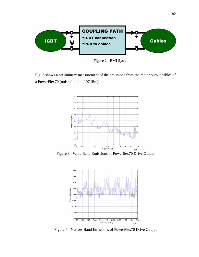
82
Fig. 3 shows a preliminary measurement of the emissions from the motor output cables of
a PowerFlex70 (noise floor at -107dBm).
Figure 3 - Wide Band Emissions of Powerflex70 Drive Output
Figure 4 - Narrow Band Emissions of PowerFlex70 Drive Output
0 0.5 1 1.5 2 2.5 3 3.5 4 4.5 5
x 107
-70
-65
-60
-55
-50
-45
-40
-35
-30
Frequency (Hz)
Magnitude (
dB
m)
2.25 2.26 2.27 2.28 2.29 2.3 2.31 2.32 2.33 2.34 2.35
x 107
-130
-120
-110
-100
-90
-80
-70
-60
-50
Frequency (Hz)
Magnitude (
dB
m)
COUPLING PATH
•IGBT connection
•PCB to cables
Cables IGBT
V
Figure 2 - EMI System

83
From previous experience, the IGBT will be the presumed source of EMI energy due to
the large, fast-switching currents and proximity to a large metallic heat sink. One focus
will be on modeling the IGBT; another will be on the motor and connecting cables.
Although Rockwell Automation recommends that shielded cable be utilized to ensure
compliance, customers may use existing unshielded cable. Therefore, both types of cable
will be investigated. Mitigation techniques related to the effectiveness of suppression
ferrites and shielding will be explored.
Model development will follow the paradigm illustrated in Fig. 5. The coupling path,
cable, and motor will be modeled with geometry in mind. A one-to-one correspondence
between the equivalent circuit and the geometry will be maintained. Complete circuit
models will be developed including parasitic devices present due to system layout and
topology. These models will then be validated via a combination of numerical simulation
(CST EM Studio, CST Microwave Studio, and Ansoft Q3D) and laboratory
measurements with using vector network analyzers, impedance analyzers, time domain
reflectometers, and spectrum analyzers.

84
Figure 5 - Equivalent Circuit Modeling Paradigm
Once completed, the equivalent circuit model will allow the rapid identification of critical
common-mode current paths, and will allow EMC problems to be identified early in the
design phase. It will also allow meaningful assessment and selection of mitigation
measures such as geometry modification, ferrites and shielding.
Summary of Achievements
The teams at Rose-Hulman Institute of Technology and Missouri University of Science
and Technology split into two sub-teams in order to accomplish the assigned tasks. One
team focused on modeling the IGBT while the other worked on the motor and cables
modeling.
IGBT Module Modeling
In modeling the IGBT package (Fig. 6), the goal was to determine the parasitic
capacitances and inductances of the IGBT module and append these parasitic elements to
the circuit schematic.

85
Figure 6 - IGBT Package
The geometry of the package presents two dominant parasitic capacitances: copper area
fills to area fills and area fills to heat sink. The major copper area fills are shown in Fig.
7.
Figure 7 - Labeled Area Fills
First, we modeled these capacitances using CST Microwave Studio, a numerical
electromagnetic field solver package. The dielectric constant of the alumina substrate was
measured by sputtering a sample of the material with copper and measuring the
capacitance, plate area, and thickness of the sample. The dielectric constant and measured
substrate thickness were used in the simulations.

86
Models of each area fill were then constructed in CST Microwave Studio and their
capacitances were obtained from the -20 dB/decade impedance curve. The largest area
fill to area fill capacitance was determined to be less than 10% of the smallest area fill to
heat sink capacitance. Therefore, it was concluded that the area fill to heat sink
capacitances would dominate the capacitive coupling paths. This was confirmed in later
simulations using Ansoft Q3D Extractor, as the mutual capacitances were on the order of
a few femtofarads. The area fill to heat sink capacitance values were superimposed on the
original circuit schematic as shown in Fig. 8. The simulated values for these capacitances
are shown in Table 1.
Figure 8 - Updated IGBT Package Schematic
Table 2 – Area Fill to Heat Sink Simulated Capacitances
Region Capacitance (pF) Region Capacitance (pF)
A 34.5 G 57.3
B 38.8 H 25.6
C 19.1 I 45.1
D 15.4 J 17.3
E 16.0 K 15.1
F 35.9 L 19.3
To validate these simulations, we took laboratory measurements of the three largest area
fill to heat sink capacitances (B, G, and I) using an impedance analyzer. Images of this
setup can be found in Figs. 9 and 10. At Missouri S&T a HP4921A impedance analyzer
was used with a low-impedance test head. RHIT used a HP4294A impedance analyzer
with an auto-balancing test fixture. Fixture compensation was used in both setups (open

87
and short for Missouri S&T; open, short, and load for RHIT). The results are shown in
Table 2 below.
Table 3 – Area Fill to Heat Sink Capacitances
Region Measured (pF) Simulated (pF) % Difference
B 37.7 38.8 2.9
G 53.3 57.3 7.2
I 39.4 45.1 13.7
Figure 9 - IGBT Capacitance Measurement Setup
Figure 10 - IGBT Area Fill B Capacitance Measurement

88
Two of these capacitances agreed to within 8%. The largest region – I – was within 14%.
Region I has a long, narrow appendage which allows outside fields to interact with it, so
the margin of error is larger. However, we were still satisfied with the agreement of our
measurements and simulations, as it is within an acceptable margin of error. Knowing
that the simulations matched the measurements gave confidence in their accuracy.
The next step in modeling the IGBT package was to determine the existing common-
mode parasitic inductances. To find these scattered, more complicated parasitics, it was
needed to first determine the self-inductances of each of the three phase legs (Phase Leg
1 is shown as an example in Figures 11 and 12). Each phase leg corresponds to one of the
three phases from the positive DC rail to the output to the motor. The outputs are pins 4,
5, and 6 corresponding to phases 3, 2, and 1, respectively.
Figure 11 - Schematic of Phase Leg 1
Figure 12 - Image of Phase Leg 1: RHIT Setup

89
Figure 13 - Image of Phase Leg 2: Missouri S&T Setup
Before the partial inductances could be extracted, it was necessary to measure the entire
phase leg. First, the entire phase leg impedance was obtained in order to know the total
inductance and its corresponding impedance curve. A probe was placed on the positive
DC rail input and the output (at the location of the bond wires leading to the
corresponding output pin) was shorted to the heat sink. Three-dimensional models of
each phase leg, consisting of area fills and the bond wires connecting them, were
constructed in CST Microwave Studio. In a similar manner to the capacitance
simulations, each inductance value was extracted from the +20 dB/decade impedance
curve (see Table 3).
Once again, the simulations were validated against measurements, taken with the same
impedance analyzers as before. Two distinct methods were used to measure the total
impedance of the phase leg. The RHIT team used the original bond wires of the IGBT
module, while removing all connected bond wires not associated with the phase being
measured. They bypassed the transistor by soldering its bond wires to the area fill (See
Figure 12). The Missouri S&T team removed all bond wires and reattached copper bond
wires in the place of the originals. Then, the transistor in the phase leg was removed and
shorted (see Figure 13). The RHIT approach had the advantage of using the original setup
with accurate bond wire dimensions. The Missouri S&T approach had the advantage of
having cleaner solder joints, accurate location of bond wires, and the certainty that any
unexpected current paths (from additional bond wires) were removed. However, the

90
Missouri S&T team had difficulty reproducing the geometry of phase 2 due to the
jumping pairs of bond wires from transistor to diode found on area fill G. It was observed
that the results were greatly dependent on the bond wire geometry. It was also observed
that variations in the solder connection from the probe produced a non-negligible effect
on the results. Both methods produced the same total inductance, and all three phase legs
agreed to within 6% of the simulated value (see Table 3). These results were sufficient to
give confidence that the simulated inductances accurately reflect the actual inductances.
Table 4 – Phase Leg Inductances
Phase Leg Measured (nH) Simulated (nH) % Difference
1 13.3 13.1 1.3
2 12.1 12.8 5.6
3 9.1 8.7 4.5
In order to develop an equivalent circuit model, it was necessary to find the contribution
of each area fill and bond wire to the total common-mode inductance. Each area fill and
bond wire was modeled as its own small loop, and shorted to the heat sink. The sum of
the partial inductances in each phase leg should be equal to the total self-inductance of
that phase leg. After working with several circuit topologies for our measurement of
Phase 1 and using several different methods of simulation (CST 2006b with discrete
ports, CST 2008 with discrete face ports, and Ansoft Q3D), the most accurate model was
developed (See Figure 14). Ansoft Q3D Extractor was used to extract partial inductance
values and simulated the topology shown in Figure 14 using Agilent Advanced Design
System (ADS) software. It was found that the result matched well with the measured
impedance curve, as shown in Figure 15. The extracted data is included in Table 4.
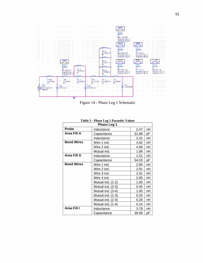
91
Figure 14 - Phase Leg 1 Schematic
Table 5 - Phase Leg 1 Parasitic Values
Phase Leg 1
Probe Inductance 2.47 nH
Area Fill A Capacitance 31.88 pF
Inductance 2.41 nH
Bond Wires Wire 1 ind. 4.62 nH
Wire 2 ind. 4.66 nH
Mutual ind. 1.89 nH
Area Fill G Inductance 1.51 nH
Capacitance 54.03 pF
Bond Wires Wire 1 ind. 2.95 nH
Wire 2 ind. 2.91 nH
Wire 3 ind. 2.91 nH
Wire 4 ind. 2.95 nH
Mutual ind. (1-2) 1.00 nH
Mutual ind. (2-3) 0.45 nH
Mutual ind. (3-4) 1.00 nH
Mutual ind. (1-3) 0.25 nH
Mutual ind. (2-4) 0.26 nH
Mutual ind. (1-4) 0.14 nH
Area Fill I Inductance 3.78 nH
Capacitance 39.58 pF

92
Figure 15 - Phase 1 Impedance: Modeled vs. Measured Impedance
After Phase 1 was successfully modeled, Phases 2 and 3 were modeled using the same
method. In order to reduce the complexity of the final model, the individual bond wires
and their corresponding mutual inductances were modeled as a single inductor. The
models and results are shown in Figures 16-19. The data is included in Tables 5 and 6.
Figure 16 - Phase 2 Model
106
107
108
109
-40
-20
0
20
40
60
80
Frequency (Hz)
Impedance (
dB
)
Impedance of IGBT Phase Leg 1
Measured Impedance
Model w/ Q3D Values
106
107
108
109
-100
-50
0
50
100
Frequency (Hz)
Phase(d
egre
es)

93
Table 6 - Phase Leg 2 Parasitic Values
Phase Leg 2
Probe Inductance 2.47 nH
Area Fill A Capacitance 33.00 pF
Inductance 2.35 nH
Bond Wires Inductance 3.35 nH
Area Fill G Inductance 4.71 nH
Capacitance 55.20 pF
Bond Wires Inductance 4.71 nH
Area Fill H Inductance 2.50 nH
Capacitance 22.30 pF
Figure 17 - Phase 2 Modeled vs. Measured Impedance
106
107
108
109
-40
-20
0
20
40
60
80
Frequency (Hz)
Impedance (
dB
)
Impedance of IGBT Phase Leg 2
Measured Impedance
Model w/ Q3D Values
106
107
108
109
-100
-50
0
50
100
Frequency (Hz)
Phase(d
egre
es)

94
Figure 18 - Phase 3 Model
Table 7 - Phase Leg 3 Parasitic Values
Phase Leg 3
Probe Inductance 2.47 nH
Area Fill A Capacitance 33.40 pF
Inductance 1.11 nH
Bond Wires Inductance 3.54 nH
Area Fill F Inductance 4.40 nH
Capacitance 32.30 pF
Figure 19 - Phase 3 Modeled vs. Measured Impedance
106
107
108
109
-40
-20
0
20
40
60
80
Frequency (Hz)
Impedance (
dB
)
Impedance of IGBT Phase Leg 3
Measured Impedance
Model 2 w/ Q3D Values
106
107
108
109
-100
-50
0
50
100
Frequency (Hz)
Phase(d
egre
es)

95
With the rush to obtain a final equivalent circuit model for initial testing, the simulations
and models were not refined to obtain a closer match because efforts were diverted to
extracting the parasitic values for the intentional current paths. Part of the mismatch in
Phase 2 may be because the jumping bond wires across the transistor and diode on area
fill G were extremely hard to reproduce in the Missouri S&T measurement setup
(compare Figures 12 and 13)
The intentional current paths included at least 8 different loops for each phase leg. Four
(two complete loops per schematic, shown in red) of these loops are shown in Figure 20.
Figure 20 - Several Phase 1 Intentional Current Paths
The third set of current paths (shown in green in Figure 20) includes the current path
through the flyback diodes. The last two current paths are not shown but represent the
case when all the upper transistors are on or when all the lower transistors are on.
on
on on
on
on on

96
A model of the entire IGBT was put together. First, Solidworks was used to model the
area fill geometry. An image of the IGBT was overlaid on the model and the area fill
geometry was traced and extruded. This file was imported into CST, the bond wires were
created, and the final model (see Figure 21) was imported into Q3D for simulation. As
Q3D allows the user to exclude objects from the simulation, the entire model will be the
base for future simulations.
Figure 21 - Entire IGBT Model
As this modeling is beyond the scope of our work, the results are not currently included.
When the simulations are completed for both the negative DC rail common-mode partial
inductances and the intentional current path partial inductances, these will be placed in
the final PSpice model for testing.
Motor and Cables The main goal of the motor and cables team was to formulate and test methods for
suppressing electromagnetic interference that emerges from an AC motor drive at the
motor and cables. To achieve this goal, we began constructing various test setups as a
means to develop a model for the motor and cables. From this model, we can simulate
suppression methods, and verify their effectiveness.
One of the first important parameters to characterize the motor and cables was to find the
input impedance. A drawing of the test setup that was used to find this for the unshielded
cables is shown in Fig. 22, where pictures of the actual test setup are included in Figures

97
23 - 25. The test setup had an aluminum plane that formed the base of the setup and also
served as a return plane for the common mode current. In addition to the aluminum return
plane, there was an aluminum block beneath the motor to keep the motor securely
mounted. The motor was wired for high voltage and the wires rested on insulation foam
to separate them from the grounding plane by 10cm as specified by the CISPR standards.
In addition, the insulation foam was used to keep the return plane level. At the opposite
end of the return plane, approximately 8.5 feet away from the motor, was an „L‟ shaped
aluminum plate fastened to the return plane with copper tape. An N-type bulkhead
connector was mounted to the plate, and all three phase wires were soldered to the inner
conductor of the connector; copper tape was used to reinforce and ensure a good
connection to the return plane. The opposite end of the N-type bulkhead connector
allowed a connection for one port measurements.
Figure 22 - Motor and Cable Test Setup
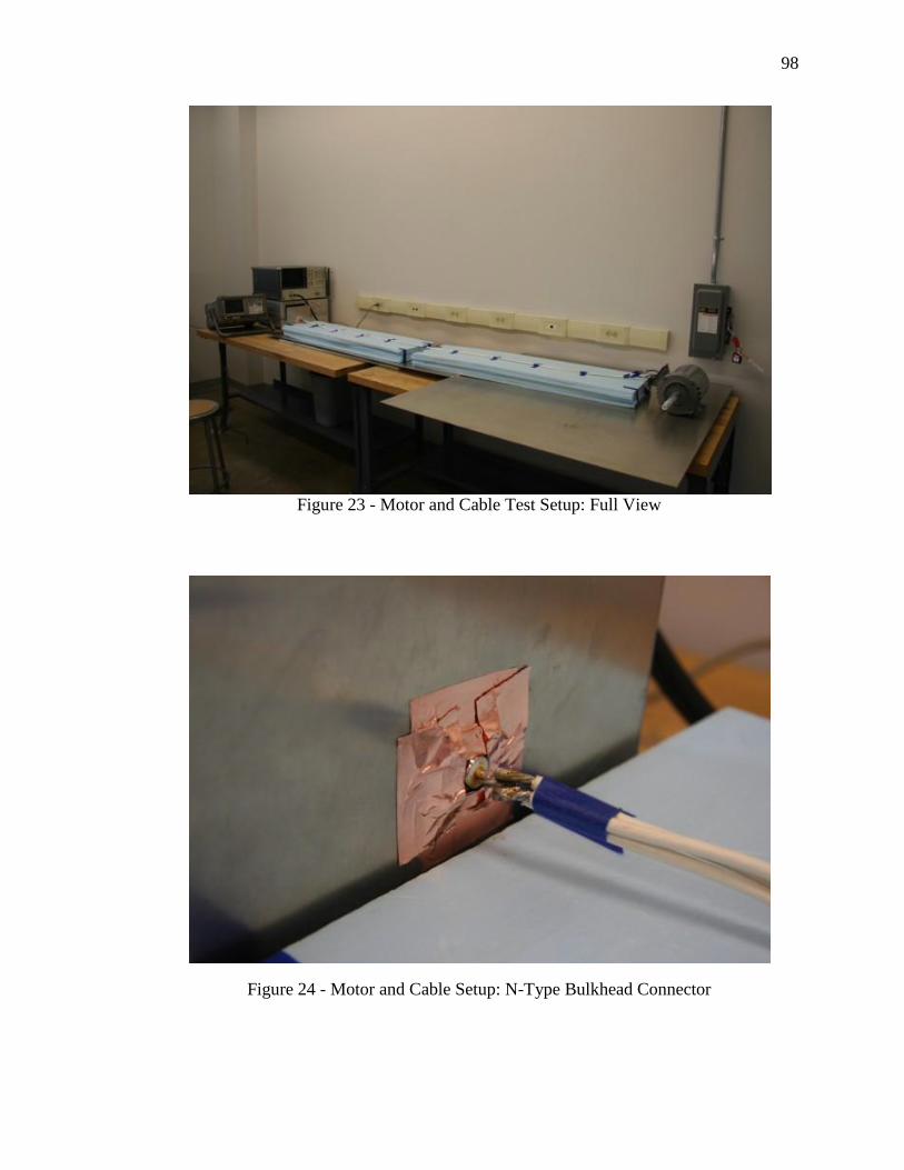
98
Figure 23 - Motor and Cable Test Setup: Full View
Figure 24 - Motor and Cable Setup: N-Type Bulkhead Connector
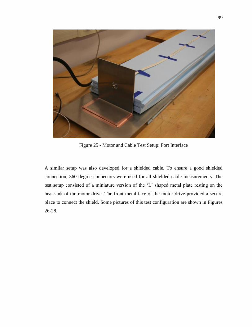
99
Figure 25 - Motor and Cable Test Setup: Port Interface
A similar setup was also developed for a shielded cable. To ensure a good shielded
connection, 360 degree connectors were used for all shielded cable measurements. The
test setup consisted of a miniature version of the „L‟ shaped metal plate resting on the
heat sink of the motor drive. The front metal face of the motor drive provided a secure
place to connect the shield. Some pictures of this test configuration are shown in Figures
26-28.

100
Figure 26 - Shielded Motor and Cable Test Setup: Full View
Figure 27 - Shielded Motor and Cable Test Setup: One Port Interface

101
Figure 28 - Shielded Motor and Cable Test Setup: Motor Wiring
The input impedance of the motor and cables was found with an Agilent 8753ES network
analyzer at Missouri S&T and an HP4294A impedance analyzer at RHIT. Figure 29
shows the shielded and unshielded input impedance as a function of frequency. As can be
seen by the data, at low frequencies the motor and cables are capacitive, whereas in the
higher frequencies the motor and cables switch between being inductive and capacitive. It
is in the higher frequencies that the characteristics of the cables dominate. One
observation from the input impedance data in Figure 29 is that the capacitance of the
shielded cable is much higher than the unshielded cable. At 300 kHz, the capacitance of
the shielded cable is 10.61nF compared to .71nF for the unshielded cable. The increased
capacitance in the shielded motor and cable setup makes sense since a possible return
path (the shield) is much closer to the three phase wires than the single return plane in the
unshielded setup.
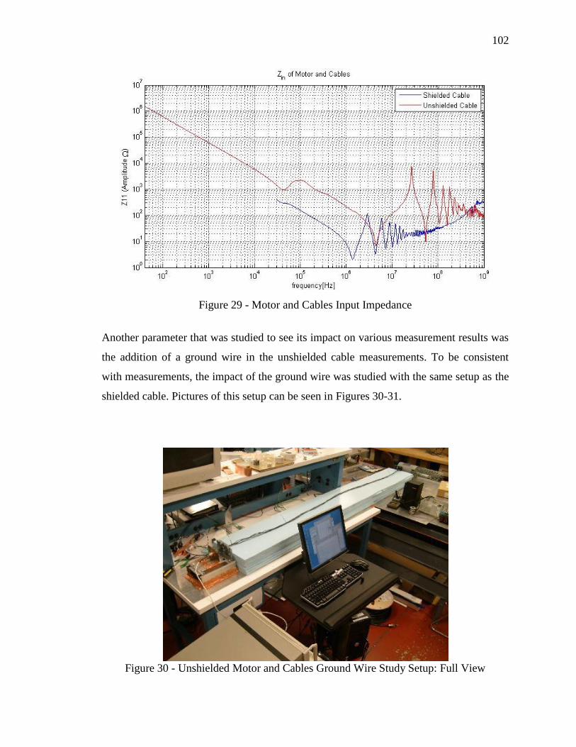
102
Figure 29 - Motor and Cables Input Impedance
Another parameter that was studied to see its impact on various measurement results was
the addition of a ground wire in the unshielded cable measurements. To be consistent
with measurements, the impact of the ground wire was studied with the same setup as the
shielded cable. Pictures of this setup can be seen in Figures 30-31.
Figure 30 - Unshielded Motor and Cables Ground Wire Study Setup: Full View

103
Figure 31 - Unshielded Motor and Cables Ground Wire Study Setup: One Port Interface
To see the effect of changing setups for the unshielded cable measurements, a
comparison of the results without the ground wire can be seen in Figure 32. It was found
that changing setups had a negligible impact on the results.
Figure 32 - Unshielded Motor and Cables Laboratory Setup Change Study

104
The results of the ground wire input impedance study can also be found in Figure 33. The
most noticeable impacts that adding a ground wire appeared to have is moving the first
resonant frequency higher by a few megahertz and creating more resonance above 40
MHz.
Figure 33 - Unshielded Motor and Cables Ground Wire Study
With the input impedance of the motor and cables identified, the emissions from the
motor drive were next studied. The motor drive was connected to 480V and to the motor
and cables. We used a Rohde&Schwarz 1066.3010.30 spectrum analyzer in conjunction
with an F-62 current probe to capture the emissions through a common mode current
measurement. Pictures of the test setup are included in Figures 34-36.

105
Figure 34 - Emissions Test Setup: Motor Drive, Spectrum Analyzer, Amplifier, and
Current Probe
Figure 35 - Emissions Test Setup: Motor and Cables

106
Figure 36 - Emissions Test Setup: Close-up
Emissions measurements were taken with various ferrites attached to the cables as shown
in the Fig. 37.
Figure 37 - Ferrite Placement

107
A critical aspect to making the common mode current measurement was placing an
amplifier between the current probe and the spectrum analyzer. The role of the amplifier
was to serve as a means of protection for the spectrum analyzer. In the case of an
accidental short at the motor drive, the amplifier would act as a fuse, destroying the
amplifier instead of the spectrum analyzer. The amplifier started to saturate around -
20dBm. A plot of the amplifier gain and phase versus frequency are shown below in
Figures 38-39.
Figure 38 - Amplifier Gain vs. Frequency
Figure 39 - Amplifier Phase vs. Frequency

108
We noticed that there were a significant amount of emissions when the motor was not
running and power was applied to the motor drive. With this in mind the power readings
from the spectrum analyzer when the motor was running are compared to the trace when
power was applied to the motor drive, but with the motor not running. The common
mode current measurements have the units of dBm since the current probe impedance is
not factored out of the data. In addition to this, effects from the amplifier are not factored
out of the data. The common mode current measurements are shown in Figures 40-45.
Figure 40 - Unshielded Common Mode Current Measurements: Noise Level
Identification

109
Figure 41 - Unshielded Common Mode Current Measurements (No Ground Wire)
Figure 42 - Unshielded Common Mode Current Measurements (With Ground Wire)

110
Figure 43 - Unshielded Common Mode Current Measurements (No Ground Wire):
Impedance/Emissions Comparison
Figure 44 - Unshielded Common Mode Current Measurements (With Ground Wire):
Impedance/Emissions Comparison

111
Figure 45 - Shielded Common Mode Current Measurements: Impedance/Emissions
Comparison
In the common mode current measurements, the main ferrite that was tested was the
Ferrishield CS33B2000. Although other ferrites were tested with the unshielded cable,
the CS33B2000 was one of the few that could fit around both sets of cables. To better
understand how ferrites helped reduce the common mode current, the input impedance of
the motor and cables were studied with various ferrites attached. With the setup shown in
Fig. 23, the input impedance was determined with the network analyzer at Missouri S&T
and an impedance analyzer at RHIT. The effects of the ferrites placed at different points
on the cables are shown in Figures 46-49. We mainly cared about ferrites placed in close
proximity to the plate. The results obtained in Figures 48-49 were mainly done out of
curiosity. The data in Figures 46-47 shows that the ferrites increased the impedance in
specific frequency bands. Fig. 50 is a specification sheet from Ferrishield showing the
impedance characteristics of the CS33B2000 ferrite.

112
Figure 46 - Effects of Ferrites 1 inch from Plate
Figure 47 - Effects of Ferrites 1 inch from Plate
10 20 30 40 50 60 70 80 90 10020
30
40
50
60
70
80
Impedance & Phase of Line
Ferrites Placed 1 inch from Plate
Loga
rithm
ic I
mpe
danc
e (
dB)
10 20 30 40 50 60 70 80 90 100
-90
-45
0
45
90
Pha
se (
o )
Frequency (MHz)
No Ferrite
CS1937
SS2032
28A2029
SS2036

113
Figure 48 - Effects of Ferrites 50 inches from Plate
10 20 30 40 50 60 70 80 90 10020
30
40
50
60
70
80
Impedance & Phase of Line
Ferrites Placed 50 inches from Plate
Logarith
mic
Im
pedance (
dB)
10 20 30 40 50 60 70 80 90 100
-90
-45
0
45
90
Phase (
o)
Frequency (MHz)
No Ferrite
CS1937
SS2032
28A2029
SS2036

114
Figure 49 - Effects of Ferrites 95 inches from Plate
Figure 50 - CS33 Series Ferrishield Ferrite Impedance Characteristics
As can be seen by the input impedance plots, ferrites can help reduce common mode
current because they increase the impedance over a frequency range. For this reason, it is
10 20 30 40 50 60 70 80 90 10020
30
40
50
60
70
80
Impedance & Phase of Line
Ferrites Placed 95 inches from Plate
Logarith
mic
Im
pedance (
dB)
10 20 30 40 50 60 70 80 90 100
-90
-45
0
45
90
Phase (
o)
Frequency (MHz)
No Ferrite
CS1937
SS2032
28A2029
SS2036

115
important to look at the data sheets similar to Fig. 50 before using ferrites. Ferrites are the
most effective when they add impedance to frequencies where the input impedance of the
motor and cables are low. Wherever the ferrites increase the impedance of the line, they
will reduce the emissions as well as Figures 41-45 show. These figures illustrate only a
small decrease in common mode current, and this can be explained by the fact that the
ferrite used does not add much impedance. Referring to Fig. 50, at its peak value the
CS33B2000 ferrite only adds 200Ω which is small compared to the peak impedances
which are above 1kΩ.
To better evaluate possible EMI mitigation strategies, a model for the motor and cables
was developed. To model the motor, the IEEE paper, “Efficient HF Modeling and Model
Parameterization of Induction Machines for Time and Frequency Domain Simulations”
was referenced. This paper outlines a method for the creation of a high frequency model
for an induction motor. A complete model for the induction motor was generated from
the data from two types of impedance measurements: common-mode and differential-
mode. Pictures showing the setup for both the common-mode and differential-mode
measurements are shown in Figures 51-55.
Figure 51 - Common Mode Setup: Full View A

116
Figure 52 - Common Mode Setup: Full View B
Figure 53 - Common Mode Setup: Common Mode Connection

117
Figure 54 - Differential Mode Setup: Full View
Figure 55 - Differential Mode Setup: Differential Mode Connection

118
The impedance measurements for each setup are shown in Figures 56-57.
Figure 56 - Common Mode Measurement: Impedance and Phase
102
103
104
105
106
107
108
100
101
102
103
104
105
106
107
Measurement
Common Mode
Impe
danc
e (
)
1X
2X
3 X
102
103
104
105
106
107
108
-90
-45
0
45
90
Pha
se (
o )
Frequency (Hz)
-85.9X-89.7
X
-34.7X

119
Figure 57 - Differential Mode Measurement: Impedance and Phase
As instructed by the paper, data points from both sets of measurements are used to
calculate component values for the motor model. Using the formulas given in the paper,
motor model as shown in Fig. 58, was created.
102
103
104
105
106
107
108
101
102
103
104
105
Measurement
Differential Mode
Impedance (
)
AX
BX
C X
102
103
104
105
106
107
108
-90
-45
0
45
90
Phase (
o)
Frequency (Hz)
82.2X
-4.5X
0.2X
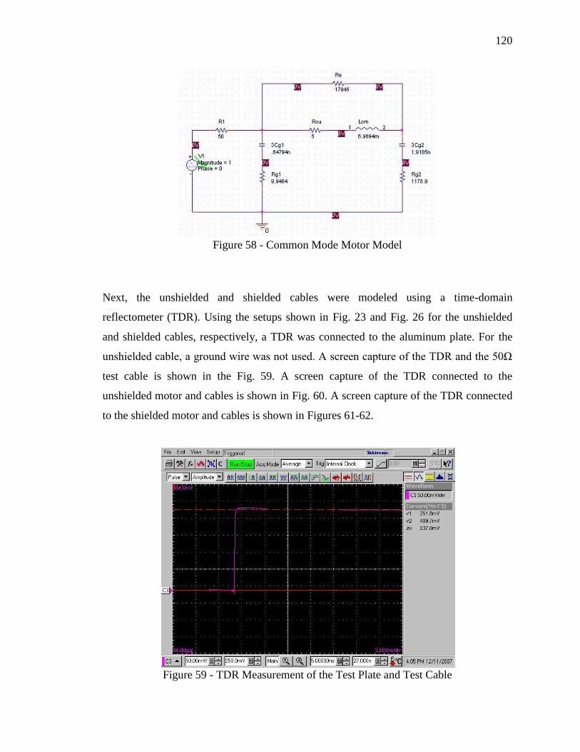
120
Figure 58 - Common Mode Motor Model
Next, the unshielded and shielded cables were modeled using a time-domain
reflectometer (TDR). Using the setups shown in Fig. 23 and Fig. 26 for the unshielded
and shielded cables, respectively, a TDR was connected to the aluminum plate. For the
unshielded cable, a ground wire was not used. A screen capture of the TDR and the 50Ω
test cable is shown in the Fig. 59. A screen capture of the TDR connected to the
unshielded motor and cables is shown in Fig. 60. A screen capture of the TDR connected
to the shielded motor and cables is shown in Figures 61-62.
Figure 59 - TDR Measurement of the Test Plate and Test Cable

121
Figure 60 - TDR Measurement of the Motor and Cables
Figure 61 - Shielded Cable TDR Measurement

122
Figure 62 - Shielded Cable TDR Measurement
Using these screen captures the RHIT team approximated the characteristic impedance of
the unshielded line to be 234Ω. With some theory, assuming that all three phase wires
acted as one conductor over a return plane, the characteristic impedance was calculated as
263Ω. This results in a percent error of about 12% which is acceptable for the given
assumptions in the calculation. In the same experiment as Missouri S&T, the
characteristic impedance shown by the TDR was approximately 250Ω. Using the same
theory, the theoretical value for the characteristic impedance was found to be 274Ω,
approximately resulting in a 10% error. The difference in measurement results can be
attributed to variations in the test setup, instrumentation, and the instrument calibration.
A summary of the test results found by Missouri S&T are given below in Table 7.
Table 7 – Summary of TDR Results
Cable Type Z0 (Ω) TD (ns) Cable Length (ft)
Shielded 19.5 153.793 99.5
Unshielded 250 8.841 8.35
The TDR was also used in calculating the relative permittivity of the surrounding non-
homogenous media which mostly consists of air and the insulation foam. The screen

123
capture in Fig. 63 shows a closer view of the reflected waves on the motor and cable
setup during the test. The dip in the voltage at the far right of the scope represents a
ferrous bar placed on the line. The two vertical red lines represent the N-type bulkhead
mount and the ferrous bar. With the markers the amount of time for a wave to travel (time
delay) on the line from the plate to the bar is known. By knowing the length of the line
we can calculate the velocity of propagation and then the relative permittivity. For this
method of calculation, the relative permittivity was found to be about 1.03 and supports
initial suspicions that it would be close to 1 because most of the surrounding media is air
as well as the insulation foam material used to support the cables is comprised mostly of
air.
Figure 63 - TDR Measurements for Permittivity Calculation
Although the TDR can be used to calculate the relative permittivity of the surrounding
environment, it is not necessarily the most accurate. Because there can be some
ambiguity as to the starting and ending points of the cables on the TDR, the time delay
can be thrown off by fractions of a nanosecond causing significant errors in the relative
permittivity calculation. Another way to calculate this parameter is by performing a

124
resonance analysis of the input impedance of the motor and cables from Fig. 33. In
transmission line theory, it is known that one of the resonant points represents the
frequency in which the transmission line is one quarter wavelength long. Assuming the
wave velocity was approximately equal to the speed of light in air and calculating the
quarter wavelength for a few resonant frequencies, it was found that the second resonant
point located at 26.3 MHz was most nearly the frequency that made the cables a quarter
wavelength long. Assuming the environment acted as a loss-less dielectric and from
knowing the fact that the wavelength of a wave in a loss-less dielectric is equal to the free
space wavelength over the square root of the relative permeability and permittivity, the
relative permittivity was calculated. The result of this calculation showed the relative
permittivity as 1.25.
Given the transmission line model parameters in Table 7 and the motor model in Fig. 58,
both sets of information were combined to form a motor and cable model. The unshielded
common mode motor and cable model is shown in Fig. 64. The shielded motor and cable
model is similar to the unshielded model, except the time delay and characteristic
impedance of the transmission line are different.
Figure 64 - PSpice Model of Motor and Cable

125
Using the common mode motor and cable model the measured impedance was compared
to the simulated impedance for both the unshielded and shielded models. The results are
in Figures 65-66.
Figure 65 - Comparison of Unshielded Motor and Cables Input Impedance
Figure 66 - Comparison of Shielded Motor and Cables Input Impedance

126
Deliverables
A PSPICE model of the EMI coupling paths in the PowerFlex70 together with
o Computer simulations
o Laboratory measurements
A technical report including
o Documentation and demonstration of EMC model creation
o Documentation and demonstration of developing computer simulations
o Documentation and demonstration of laboratory measurements
o Potential EMI mitigation techniques
Recommendations
IGBT Module
In the next few weeks, the teams will work to finalize the parasitic model and hand this
portion of the project over to the client. At this point we will discuss with the client future
improvements upon both the design of similar IGBT modules, as well as EMC modeling
practices and mitigation techniques.
The results of this investigation will significantly aid the client in preventing EMC
problems in the future. A starting example is that identical phase legs should have very
similar geometry. Because each of the phase legs is to perform the same duty, the
impedance should be the same, which directly correlates to its geometry. Next, noisy
currents need to have their return paths very close as to cancel out the magnetic field.
Motor and Cables
After modeling the setup and analyzing the collected data we have formulated several
ideas for mitigating emissions. In the case of unshielded cable, a simple remedy is to
attach a ferrite to the cable closest to the motor drive. The ferrites should have the highest
spectral impedance near the proper frequency. Multiple ferrites can be paired in series if
necessary for multiple frequencies. If it is possible, the best option is to use a shielded
cable since it significantly reduces emissions. Shielding is known to mitigate electric

127
fields by displacing charge on the conductor induced by the field. A simple method for
reducing differential mode conductive emissions is to twist the wires together. This
works under the assumption that the returning signal is out of phase with the departing
signal and they cancel each other.
For groups looking to further investigate this project, we believe the current model is
sufficient for simulation purposes and does not warrant further refinement. However,
there is much unexplored research on mitigation techniques. We recommend that future
groups investigate research and develop efficient, cost effective solutions.
Conclusion
EMC modeling is essential for government compliance and robust design. Engineers can
utilize models and augmented schematics to design device layout and geometry in order
to minimize EMI. As an example, we have modeled an AC motor drive. An EMC model
including parasitic capacitances and inductances for an IGBT package has been
developed and validated with simulation and laboratory measurements. In addition a high
frequency model for the motor and a transmission line model for the cables has also been
developed and verified. If used correctly, these models of a Rockwell Automation AC
motor drive and the processes used to generate them will give Rockwell Automation
engineers the necessary tools to solve future EMI problems in their products.

128
Appendix A: References
[1] Allen-Bradley, "Drives," [Online document], 2007 Aug 1, [cited 2007 Aug 1],
Available HTTP: http://www.ab.com/drives/
Rockwell Automation’s Allen-Bradley product line of motor drives is described here in
detail. Applications, specifications, as well as product support and literature is included
on this website.
[2] FCC Part 15, Radio Frequency Devices.
This dictates the FCC regulations on electronic devices and emission levels. It breaks
devices into categories, discusses types of emissions, as well as where the device will
operate. It goes into great detail on the size, power level, and measurement techniques of
various electronic devices.
[3] IEC CISPR, Electromagnetic Compatibility: Including Radio Interference.
The International Engineering Consortium requirements for the radiation emissions for
electronic devices to be used internationally are included in the body of this report. In
addition, immunity and other aspects to EMC are included in this document.
[4] Mohan, Undeland, and Robbins, Power Electronics: Converters, Applications and
Design, New York Wiley, 1989.
This article details the basics of IGBTs and how they are applicable to power systems as
a semiconductor package. In addition, it discusses the functioning of the device assuming
a previous knowledge of MOSFETs and BJTs.
[5] Paul, Clayton R., Introduction to Electromagnetic Compatibility, 2d ed. New Jersey:
John Wiley & Sons, 2006, pp. 50-58, 377-557.
Dr. Clayton Paul is an expert in electromagnetic interference and compatibility. He is the
2005 IEEE Electromagnetics Award winner. This book provides a supreme reference for
EMC situations and problems, and provides background information for a complete
understanding of the fundamentals.
[6] "Rose-Hulman Institute of Technology," [Online document], 2007 Aug 1, [cited 2007
Aug 2], Available HTTP: http://www.rose-hulman.edu/
Rose-Hulman Institute of Technology is a private, engineering school in Terre Haute, IN.
Their website includes information on its students, programs, faculty, etc.
[7] "The University of Missouri-Rolla Electromagnetic Compatibility Consortium,"
[Online document], 2007 Aug 1, [cited 2007 Aug 1], Available HTTP:
http://www.emclab.umr.edu/
The University of Missouri-Rolla’s Electrical and Computer Engineering Departments
electromagnetic compatibility group has their work, purpose, and contacts listed on this
page.
[8] Wheeler, Ed. “Instructional Materials on Electromagnetic Compatibility, Signal
Integrity, and High Speed Design,” NSF Grant 0618494, 9/2006-8/2010.

129
This NSF Proposal discusses how Drs. Wheeler and Drewniak, et. al. are attempting to
improve the understanding of electromagnetism at an undergraduate, graduate, and
industrial level.

130
BIBLIOGRAPHY
[1] D. M. Pozar, Microwave Engineering, Ch. 2, 4, John Wiley & Sons Inc,. – 3rd
edition.
[2] Paul, Clayton R., Introduction to Electromagnetic Compatibility, 2d ed. New
Jersey: John Wiley & Sons, 2006, pp. 50-58, 377-557.
[3] "The University of Missouri-Rolla Electromagnetic Compatibility Consortium,"
[Online document], 2007 Aug 1, [cited 2007 Aug 1], Available HTTP:
http://www.emclab.umr.edu/
[4] http://www.sce.carleton.ca/faculty/chinneck/thesis.html. Organizing Your Thesis,
June 2004 (date mentioned here is the date on which the website was last visited).

131
VITA
Clint Matthew Patton was born in Sedalia, MO on February 14, 1984. He
completed his general education at State Fair Community College in Sedalia, MO, from
August 2002 to May 2004. In August 2004, he transferred to the University of Missouri
in Rolla, MO where he completed his Bachelor of Science Degree in Electrical
Engineering in May 2007. He started working with the University of Missouri-Rolla
Electromagnetic Compatibility Laboratory in August 2006 performing undergraduate
research dealing with constructing antennas for measuring the shielding effectiveness of a
system. May 2007 he joined the EMC Laboratory at Missouri University of Science and
Technology in Rolla, MO, and started his Master of Science Degree in Electrical
Engineering with an emphasis in Electromagnetic Compatibility. August 2009 he
attained his Master of Science Degree and took a position with BAE Systems in Nashua,
New Hampshire, as an EMC Engineer. The research completed gave him an
understanding of how to model and extract parasitic elements that influence a circuit. He
achieved a deep understanding of full-wave modeling tools and learned how they worked
along with their limitations. For the later part his time with the EMC Laboratory, he
explored factors which play a role in the performance of devices that impose strong
magnetic fields into other systems.

132