influence of gamma irradiation on silicon nitride mis capacitors and radiation hardness dr. ercan...
TRANSCRIPT
INFLUENCE OF GAMMA IRRADIATION ON SILICON NITRIDE MIS CAPACITORS AND RADIATION
HARDNESS
Dr. Ercan YILMAZAbant Izzet Baysal University
Bolu-Turkey
Contents
• Basic Properties of Dielectrics
• Radiation Hardness
• Silicon Nitride Thin Films
• Radiation Interactions with Silicon Nitride Thin Films
• Results
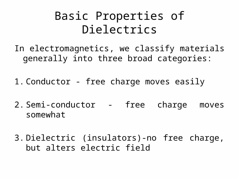
Basic Properties of Dielectrics
In electromagnetics, we classify materials generally into three broad categories:
1. Conductor - free charge moves easily
2. Semi-conductor - free charge moves somewhat
3. Dielectric (insulators)-no free charge, but alters electric field
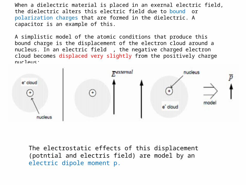
When a dielectric material is placed in an exernal electric field, the dielectric alters this electric field due to bound or polarization charges that are formed in the dielectric. A capacitor is an example of this. A simplistic model of the atomic conditions that produce this bound charge is the displacement of the electron cloud around a nucleus. In an electric field , the negative charged electron cloud becomes displaced very slightly from the positively charge nucleus:
The electrostatic effects of this displacement (potntial and electris field) are model by an electric dipole moment p.
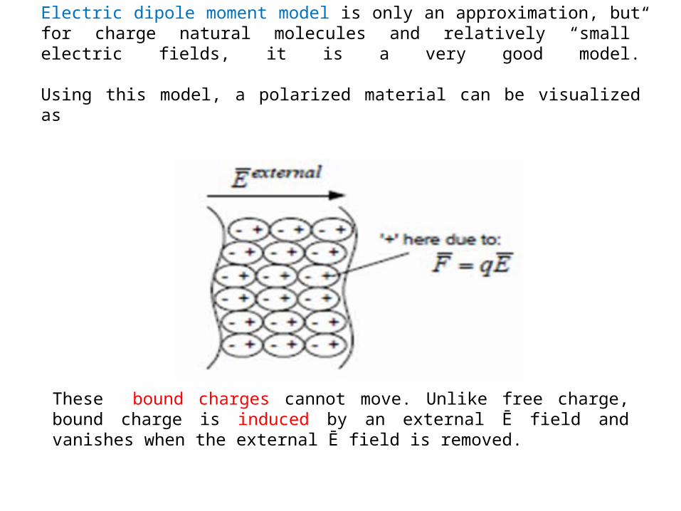
Electric dipole moment model is only an approximation, but for charge natural molecules and relatively “small” electric fields, it is a very good model.
Using this model, a polarized material can be visualized as
These bound charges cannot move. Unlike free charge, bound charge is induced by an external Ē field and vanishes when the external Ē field is removed.
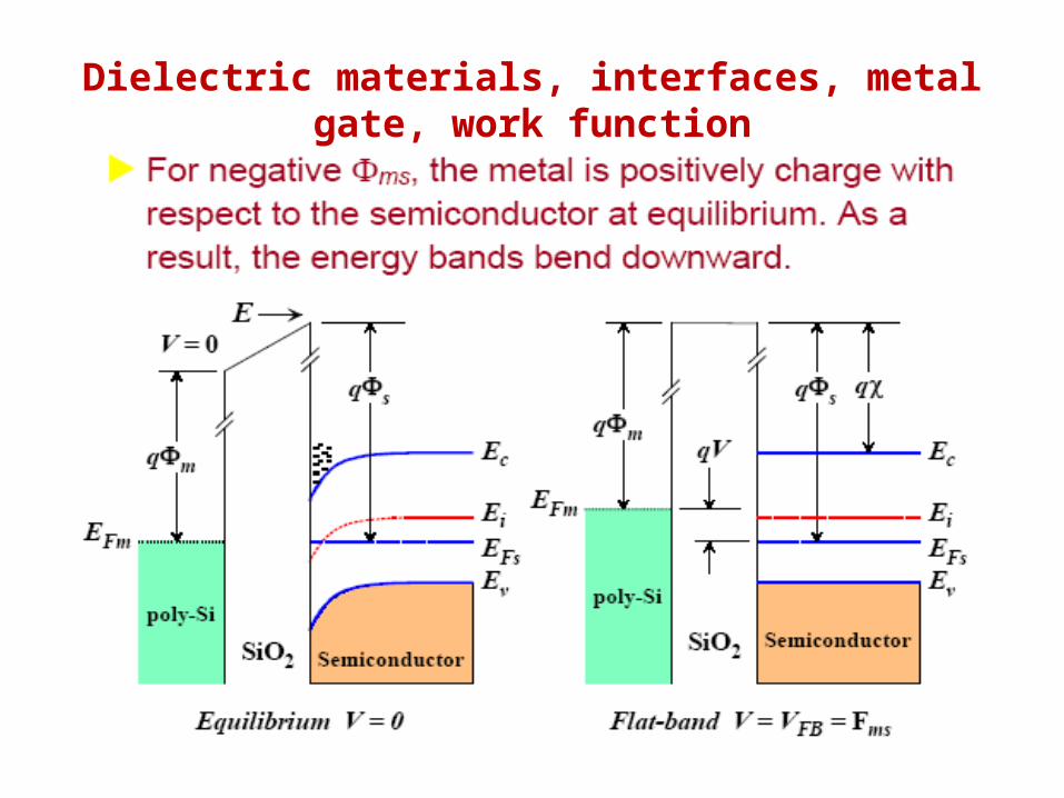
Dielectric materials, interfaces, metal gate, work function
Radiation Hardness/HardeningRadiation hardening is a method of designing and testing electronic components and systems to make them resistant to damage or malfunctions caused by ionizing radiation (particle radiation and high-energy electromagnetic radiation).
CCDs were generally expected to exhibit radiation tolerance comparable with other CMOS circuits.
Some experiments with Co-60 irradiation shows loss of charge transfer performance at doses of 10krads [Lumb and Holland 1988b].
These studies also shows that the charge transfer degradation is a more severe problem than conventional integrated circuit damage mechanisms.
Detailed experiments with proton irradiation show that displacement damage creates measurable loss of charge transfer efficiency at doses as low as 10's rads, and hence radiation hardening will require optimized shielding and CCD architectures to minimize loss of data.
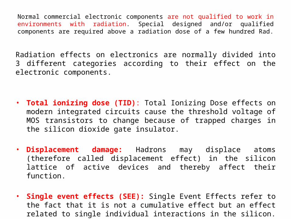
Normal commercial electronic components are not qualified to work in environments with radiation. Special designed and/or qualified components are required above a radiation dose of a few hundred Rad.
Radiation effects on electronics are normally divided into 3 different categories according to their effect on the electronic components.
• Total ionizing dose (TID): Total Ionizing Dose effects on modern integrated circuits cause the threshold voltage of MOS transistors to change because of trapped charges in the silicon dioxide gate insulator.
• Displacement damage: Hadrons may displace atoms (therefore called displacement effect) in the silicon lattice of active devices and thereby affect their function.
• Single event effects (SEE): Single Event Effects refer to the fact that it is not a cumulative effect but an effect related to single individual interactions in the silicon. Highly ionizing particles can directly deposit enough charge locally in the silicon to disturb the function of electronic circuits.
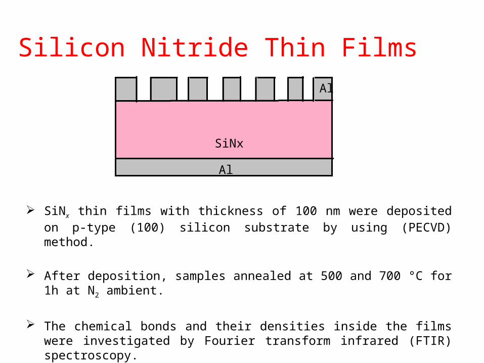
Silicon Nitride Thin Films
SiNx thin films with thickness of 100 nm were deposited on p-type (100) silicon substrate by using (PECVD) method.
After deposition, samples annealed at 500 and 700 °C for 1h at N2 ambient.
The chemical bonds and their densities inside the films were investigated by Fourier transform infrared (FTIR) spectroscopy.
Al
SiNx
Al
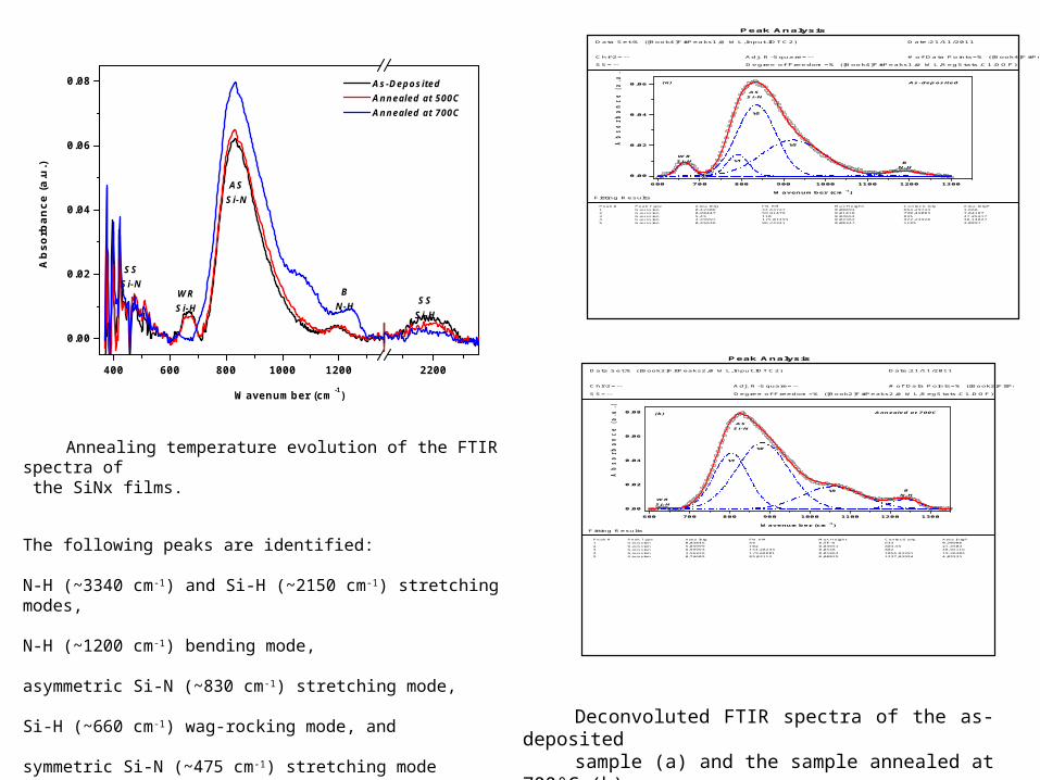
Annealing temperature evolution of the FTIR spectra of the SiNx films.
The following peaks are identified:
N-H (~3340 cm-1) and Si-H (~2150 cm-1) stretching modes,
N-H (~1200 cm-1) bending mode,
asymmetric Si-N (~830 cm-1) stretching mode,
Si-H (~660 cm-1) wag-rocking mode, and
symmetric Si-N (~475 cm-1) stretching mode
600 700 800 900 1000 1100 1200 1300
0.00
0.02
0.04
0.06
3
2
1 BN-H
ASSi-N
WRSi-H
Absorbance (a.u.)
Wavenumber (cm-1)
Peak Analysis
As-deposited(a)
Adj. R-Square=-- # of Data Points=% ([Book4]FitPeaks1,@WL,RegStats.C1.N)
Degree of Freedom=% ([Book4]FitPeaks1,@WL,RegStats.C1.DOF)SS=--
Chi 2=--
Date:21/11/2011Data Set:% ([Book4]FitPeaks1,@WL,Input.IDTC2)
Fitting Results
Max Height0,008930,014180,046540,023620,00347
Area IntgP3,6687,8418747,2521738,148273,0897
FWHM44,5372759,91479110175,0149396,74341
Center Grvty664,29743790,49003835922,239281185
Area Intg0,423060,904475,454,399970,35636
Peak TypeGaussianGaussianGaussianGaussianGaussian
Peak #12345
600 700 800 900 1000 1100 1200 1300
0.00
0.02
0.04
0.06
0.08
Absorbance (a.u.)
Wavenumber (cm-1)
Peak Analysis
BN-H
3
1
2
ASSi-N
WRSi-H
Annealed at 700C(b)
Adj. R-Square=-- # of Data Points=% ([Book2]FitPeaks2,@WL,RegStats.C1.N)
Degree of Freedom=% ([Book2]FitPeaks2,@WL,RegStats.C1.DOF)SS=--
Chi 2=--
Date:21/11/2011Data Set:% ([Book2]FitPeaks2,@WL,Input.IDTC2)
Fitting Results
Max Height8,5E-40,046510,05480,018630,00825
Area IntgP0,2090827,450448,9211619,364044,05533
FWHM44102154,28233179,6880185,02112
Center Grvty633803,558821056,843911237,03954
Area Intg0,038465,049998,999933,562360,74605
Peak TypeGaussianGaussianGaussianGaussianGaussian
Peak #12345
Deconvoluted FTIR spectra of the as-depositedsample (a) and the sample annealed at 700°C (b).
400 600 800 1000 1200 2200
0.00
0.02
0.04
0.06
0.08
A
bso
rban
ce (a.
u.)
Wavenumber (cm-1)
SSSi-N
WRSi-H
ASSi-N
As-Deposited Annealed at 500C Annealed at 700C
BN-H SS
Si-H
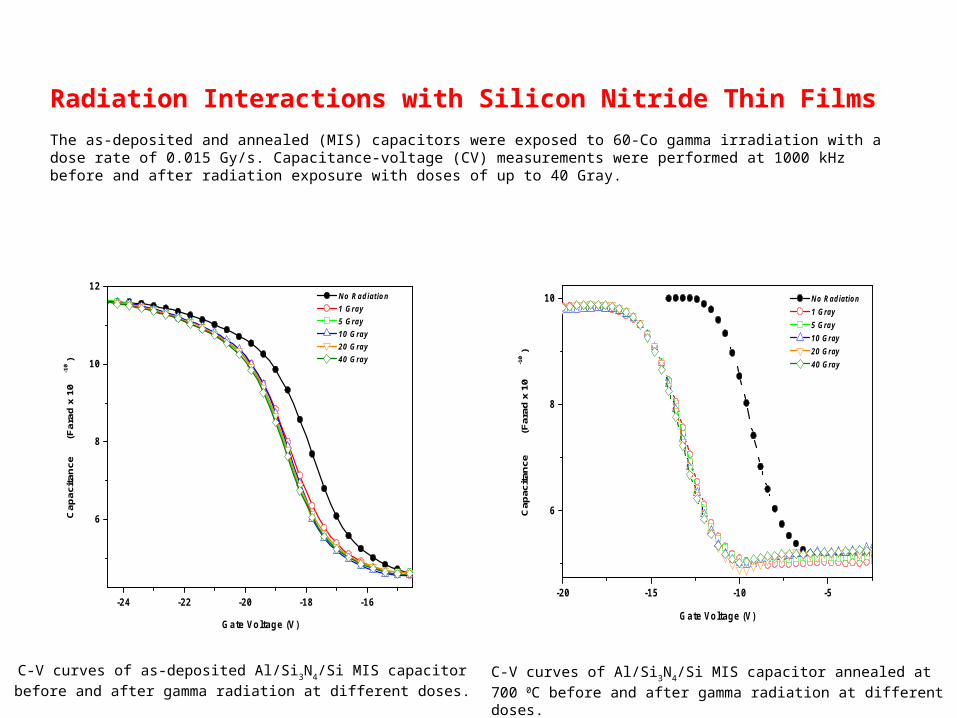
Radiation Interactions with Silicon Nitride Thin Films
The as-deposited and annealed (MIS) capacitors were exposed to 60-Co gamma irradiation with a dose rate of 0.015 Gy/s. Capacitance-voltage (CV) measurements were performed at 1000 kHz before and after radiation exposure with doses of up to 40 Gray.
-24 -22 -20 -18 -16
6
8
10
12
Cap
acita
nce
(Far
ad x
10
-10)
Gate Voltage (V)
No Radiation 1 Gray 5 Gray 10 Gray 20 Gray 40 Gray
-20 -15 -10 -5
6
8
10
Cap
acita
nce
(Far
ad x
10
-10)
Gate Voltage (V)
No Radiation 1 Gray 5 Gray 10 Gray 20 Gray 40 Gray
C-V curves of as-deposited Al/Si3N4/Si MIS capacitor before and after
gamma radiation at different doses.C-V curves of Al/Si3N4/Si MIS capacitor annealed at 700 0C before and
after gamma radiation at different doses.
Conclusions Before exposure to gamma irradiation, as-deposited sample shows relatively
large Vfb shift towards negative voltages indicating a reduction in positive charge buildup due to annealing process.
On the other hand, after gamma irradiation at different doses, all samples show a Vfb shift toward more negative values being more pronounced in the sample annealed at higher annealing temperature of 700 °C.
We attribute this to the structural characteristics of the films, in which the as-deposited sample, having an amorphous network and containing H atoms is metastable, compared with annealed samples making it less affected by irradiation.
The more streaking and common feature is observation of radiation hardening after first irradiation in as-deposited and annealed samples which can be used in space and nuclear applications as a radiation hardened device.
“If we knew what we were doing it wouldn't be research.”
Albert Einstein
THANK YOU