ingegneria elettronica, telecomunicazioni e 7(&12/2
TRANSCRIPT

AAllmmaa MMaatteerr SSttuuddiioorruumm –– UUnniivveerrssiittàà ddii BBoollooggnnaa
DOTTORATO DI RICERCA IN
INGEGNERIA ELETTRONICA, TELECOMUNICAZIONI E
TECNOLOGIE DELL’INFORMAZIONE
Ciclo XXX
Settore Concorsuale di afferenza: 09/F1
Settore Scientifico disciplinare: ING-INF/02
DESIGN AND MODELLING OF WIRELESS POWER TRANSFER
AND ENERGY HARVESTING SYSTEMS
Presentata da: Marco Fantuzzi
Coordinatore Dottorato Supervisore
Prof. Ing. Alessandro Vanelli-Coralli Prof.ssa Ing. Alessandra Costanzo
Co-supervisore
Prof. Ing. Diego Masotti
Esame finale anno 2018


Abstract
This thesis reports the main outcomes of the research activity conducted
within the Ph.D. program in Electronics, Telecommunications and In-
formation Technologies Engineering at the University of Bologna, Italy.
Close collaboration with the COST action IC1301, WIPE - Wireless
Power Transmission for Sustainable Electronics was carried on through-
out the whole duration of the Ph.D. studies. Two distinct visiting re-
search periods were completed at KU Leuven, Belgium and LCIS Labs -
Grenoble INP, France.
The escalation of the Internet-of-Everything topicality has motivated
an increased interest in both academia and industry research for efficient
solutions enabling self-sustained smart operations. From the mainte-
nance point of view, indeed, battery-less strategies represent the most
valuable way for distributed zero-power standalone electronics. With
this purpose, different scavenging techniques are being adopted, gath-
ering energy from different sources such as mechanical, solar, thermal
and electromagnetic waves. Due to the wide spread of wireless commu-
nication systems, the latter technology has recently benefited a renewed
interest. This Ph.D. research activity has been focused on the inves-
tigation of new efficient solutions for radiofrequency energy harvesting
and wireless power transmission techniques, aiming at improving the
state of the art, by also taking into account the imperative necessity of
i

Abstract
eco-friendly materials for the development of green electronics. The com-
bination of radiofrequency energy harvesting and ultra-wideband tech-
niques is also proposed as possible candidate for future RFID systems.
These functionalities are integrated in a novel, compact and low-profile
tag, whose details are provided thoroughly from both electromagnetic
and nonlinear circuit viewpoints. Results validation is provided through
experimental characterization. Compatibility with the environment is
assured by implementation with recyclable material. This concept is
then extended with the investigation of more elaborated energy scav-
enging architectures, including rectenna arrays. Finally, a near-field
wireless power transmission system is presented on low-cost materials,
therefore suitable for possible mass-market deployment.
ii

Contents
Abstract i
Contents iii
List of Figures vi
List of Tables xvi
Abbreviations xvii
Introduction xx
1 Eco-Compatible Next Generation RFID Tag 1
1.0.1 Objectives and Potential Applications . . . . . . . 3
1.1 System Architecture . . . . . . . . . . . . . . . . . . . . . 7
1.2 Integrated UWB-UHF Antenna . . . . . . . . . . . . . . . 8
1.2.1 Antenna Design . . . . . . . . . . . . . . . . . . . . 10
1.2.2 Antenna Experimental Characterization . . . . . . 16
1.3 Diplexer Network . . . . . . . . . . . . . . . . . . . . . . . 23
1.4 Taconic Implementation . . . . . . . . . . . . . . . . . . . 26
1.4.1 Antenna-Diplexer Connection . . . . . . . . . . . . 29
1.4.2 Diplexer Layout and Performance . . . . . . . . . 30
1.5 Paper Implementation . . . . . . . . . . . . . . . . . . . . 34
1.5.1 Tag UHF Performance . . . . . . . . . . . . . . . . 39
iii

Contents
1.5.2 Tag UWB Performance . . . . . . . . . . . . . . . 41
1.6 Remarks and Future Developments . . . . . . . . . . . . . 50
2 Diode Model Optimization for Simultaneous Data and
Power Transfer 52
2.1 Experimental Setup and Model Optimization . . . . . . . 55
2.2 Model Validation . . . . . . . . . . . . . . . . . . . . . . . 58
2.2.1 Frequency Validation . . . . . . . . . . . . . . . . . 59
2.2.2 Fundamental Frequency and Baseband Validation 60
2.3 Remarks and Future Developments . . . . . . . . . . . . . 63
3 Rectenna Array for Long Distance Autonomous IoT Tag
Localization 65
3.1 System Architecture . . . . . . . . . . . . . . . . . . . . . 68
3.1.1 Performance Evaluation of the Available Solution . 70
3.2 Single Rectenna Design . . . . . . . . . . . . . . . . . . . 73
3.3 Four Dipoles Rectenna Array . . . . . . . . . . . . . . . . 79
3.4 Two Monopoles Rectenna Array . . . . . . . . . . . . . . 89
3.5 Remarks and Future Developments . . . . . . . . . . . . . 94
4 Low-Cost UHF Near-Field Contactless Solution for RFID
Applications 95
4.1 WPT for RFID Applications . . . . . . . . . . . . . . . . 96
4.1.1 DGS Resonators . . . . . . . . . . . . . . . . . . . 98
4.1.2 Low-Cost Materials . . . . . . . . . . . . . . . . . 100
4.2 WPT Implementation . . . . . . . . . . . . . . . . . . . . 101
4.2.1 DGS Parametric Study . . . . . . . . . . . . . . . 103
4.2.2 Experimental Validation on Different Materials . . 106
4.3 RFID Reader Antenna . . . . . . . . . . . . . . . . . . . . 110
4.3.1 Antenna Implementation . . . . . . . . . . . . . . 110
iv

Contents
4.4 Remarks and Future Developments . . . . . . . . . . . . . 114
Conclusions 115
Acknowledgements 118
List of Achievements 119
Bibliography 124
v

List of Figures
1 Building blocks of a far-field WPT or EH system. . . . . xxiv
1.1 Representation of the GRETA system. . . . . . . . . . . 4
1.2 Example of GRETA potential application for logistics and
industrial production chain. . . . . . . . . . . . . . . . . 6
1.3 Example of GRETA potential application for smart hos-
pital. . . . . . . . . . . . . . . . . . . . . . . . . . . . . . 7
1.4 Schematic representation of the GRETA tag architecture,
where the highlighted area corresponds to the described
design activity. . . . . . . . . . . . . . . . . . . . . . . . . 8
1.5 Modeled dc output power for two comparable rectennas,
operating at 900 and 2450 MHz. . . . . . . . . . . . . . . 9
1.6 Integrated UWB-UHF one-port antenna architecture. . . 13
1.7 (a) Final topology of the proposed antenna. (b) Reac-
tance and maximum realized gain as a function of the
length of the dipole. . . . . . . . . . . . . . . . . . . . . . 14
1.8 Full-wave simulation results in terms of surface current
magnitude in the UHF and UWB bands. . . . . . . . . . 15
1.9 Antenna performance in terms of reflection coefficient,
without dipole (gray line) and with dipole (black line).
. . . . . . . . . . . . . . . . . . . . . . . . . . . . . . . . . 16
vi

List of Figures
1.10 Antenna performance in terms of realized gain in the yz-
plane at the central UWB band frequency of 4 GHz, with-
out dipole (gray line) and with dipole (black line). . . . . 17
1.11 Antenna simulated axial ratio at the central UWB band
frequency of 4 GHz, with and without dipole, in the yz-
and xz-plane. . . . . . . . . . . . . . . . . . . . . . . . . . 17
1.12 Photo of the FR-4-based prototype: (a) front view and (b)
perspective view with the coaxial cable used in radiation
pattern measurements. . . . . . . . . . . . . . . . . . . . 18
1.13 Measured and modeled antenna input impedance: (a) real
part; (b) imaginary part in the UHF band; (c) real part;
and (d) imaginary part in the UWB band. . . . . . . . . 19
1.14 Measured and modeled reflection coefficient in the UHF
band (normalized to 12 W). 0.5-l, 1.5-l, and 2.5-l reso-
nances can also be recognized. . . . . . . . . . . . . . . . 20
1.15 Measured and modeled reflection coefficient in the UWB
band (normalized to 120 W). . . . . . . . . . . . . . . . . 20
1.16 Measured and modeled normalized field radiation pat-
terns of the co- and cross-polarized component at 868
MHz, in the (a) E-plane (yz) and (b) H-plane (xz) of the
dipole. . . . . . . . . . . . . . . . . . . . . . . . . . . . . 21
1.17 Measured and modeled normalized field radiation pat-
terns at 3, 4, and 5 GHz, in the yz-plane (left column),
and in the xz-plane (right column). . . . . . . . . . . . . 22
1.18 Simulated (solid line) and measured (markers) realized
gain of the FR4-prototype in the (a) UHF band and (b)
UWB band. . . . . . . . . . . . . . . . . . . . . . . . . . 23
vii

List of Figures
1.19 Schematic of the diplexer circuit topology. Port 2 is an ar-
tificial termination introduced for evaluation of the diplexer
performance. . . . . . . . . . . . . . . . . . . . . . . . . . 24
1.20 Simulated scattering parameters of the three-port net-
work of Fig. 1.19 in the (a) UHF band and (b) UWB
band. . . . . . . . . . . . . . . . . . . . . . . . . . . . . . 25
1.21 Diplexer UHF (a) matching and (b) filtering performance
distortion during the UWB modulation (SC - Short Cir-
cuit, OC - Open Circuit). . . . . . . . . . . . . . . . . . . 27
1.22 Filter insertion loss in the UWB band for different inci-
dent UHF power levels. . . . . . . . . . . . . . . . . . . . 27
1.23 Photo of the Taconic-based prototype with the corre-
sponding dimensions. The highlighted part in the center
part of the antenna represents the diplexer area on the
backside of the tag. . . . . . . . . . . . . . . . . . . . . . 28
1.24 Representation of the antenna-diplexer connection. A re-
moval in the diplexer ground plane allows one of the two
balanced lines to reach the diplexer top layer. . . . . . . 31
1.25 Diplexer (a) layout representation and (b) photo of the re-
alized prototype. With reference to Fig. 1.19, the ground
plane aperture corresponds to port 1, which connects to
the antenna, test port corresponds to port 2 and UWB
modulator/test port corresponds to port 3. . . . . . . . . 31
1.26 Comparison between the measured and simulated reflec-
tion and transmission coefficient at ports 1 and 3 of the
Taconic diplexer. Both ports are normalized on 50 W. . . 32
viii

List of Figures
1.27 RF-to-dc conversion efficiency for low levels of RF incom-
ing available power. Inconsistent measured results are a
consequence of the inaccurate manufacturer model of the
Schottky diodes. . . . . . . . . . . . . . . . . . . . . . . . 34
1.28 Pictures of the complete tag realized on Taconic sub-
strate. . . . . . . . . . . . . . . . . . . . . . . . . . . . . 35
1.29 Tag architecture: (a) side multilayer view and (b) zoomed
perspective 3-D view, where the multiple layers are made
transparent for ease of visualization. . . . . . . . . . . . . 36
1.30 Comparison between modeled gain patterns of the stan-
dalone antenna and the antenna with the back side diplexer
at the UWB central frequency (4 GHz). . . . . . . . . . . 36
1.31 (a) Integrated UWB-UHF antenna layout. (b) Prototype
on paper substrate. . . . . . . . . . . . . . . . . . . . . . 37
1.32 Simulated and measured integrated UWB-UHF antenna
reflection coefficient with respect to 50 W (vector network
analyzer reference impedance). . . . . . . . . . . . . . . . 38
1.33 Comparison between measured and simulated antenna in-
put impedance in the UHF band, (a) real part and (b)
imaginary part. . . . . . . . . . . . . . . . . . . . . . . . 38
1.34 (a) Miniaturized diplexer layout, with area 13.2x 13.2mm2
and thickness 370µm. (b) Picture of the prototype on pa-
per substrate. . . . . . . . . . . . . . . . . . . . . . . . . 39
1.35 RF-to-dc conversion efficiency and rectified voltage on the
optimum load for typically available RF input power lev-
els. . . . . . . . . . . . . . . . . . . . . . . . . . . . . . . 41
ix

List of Figures
1.36 Comparison between measured and modeled diplexer an-
tenna port return loss and antenna-to-UWB port inser-
tion loss. Both UWB port and antenna port are referred
to 50 W terminations. . . . . . . . . . . . . . . . . . . . . 42
1.37 (a) Antenna in receiving mode. (b) Corresponding equiv-
alent circuit representation in frequency domain for the
HB analysis. . . . . . . . . . . . . . . . . . . . . . . . . . 44
1.38 Antenna distortion effects on the received pulse. (a) UWB
pulse incident on the antenna. (b) Received pulse by the
standalone antenna, for fixed polarization (ψ = 0°) and
varying incident elevation θ angle. (c) Received pulse by
the standalone antenna, for fixed AOA and two different
polarizations of the incident field. (d) Received pulse by
the standalone antenna and the complete tag with the
diplexer. . . . . . . . . . . . . . . . . . . . . . . . . . . . 45
1.39 UWB communication measurements in a real office sce-
nario. . . . . . . . . . . . . . . . . . . . . . . . . . . . . . 47
1.40 Representation of a passive backscattering communica-
tion, showing all the distinct signal components: clutter,
tag structural mode and tag antenna mode (the only one
dependent on the information). . . . . . . . . . . . . . . 48
1.41 Received measured backscattered signal amplitudes: (a)
at the oscilloscope with no processing and (b) after post-
processing, for a fixed reader-tag distance of 70 cm. . . . 49
x

List of Figures
2.1 Schematic representation of (a) a conventional, separated,
harvesting and information receiver architecture, where
two distinct nonlinear conversion units are employed and
(b) integrated harvesting and information architecture,
featuring a single nonlinear rectifying/mixing section fol-
lowed by a low-pass filter. . . . . . . . . . . . . . . . . . 53
2.2 LSNA vector-calibrated measurement setup adopted for
the single diode measurements. In the center part of the
picture it is possible to see the PCB on Rogers substrate. 56
2.3 Magnitude of the transmitted voltage waves at the third-
order (a) low and (b) high IM products around the fun-
damental frequency and respective phase (c-d). . . . . . 58
2.4 Magnitude of the transmitted voltage waves at the (a)
first and (b) second IM products in the baseband and
respective phase (c-d). . . . . . . . . . . . . . . . . . . . 59
2.5 (a) Picture of the full-wave rectifier and (b) and compari-
son between measured and modeled OC dc voltage at the
rectifier output, for a fixed input RF power of -10 dBm. . 60
2.6 (a) Picture of the single-diode rectifier, realized on 0.76
mm-thick Rogers RO3003 substrate and (b) NVNA mea-
surement setup. . . . . . . . . . . . . . . . . . . . . . . . 61
2.7 (a) dc output voltage of the single-diode rectifier for dif-
ferent values of RF input power and (b) output voltage
wave magnitude at the first IM product in the baseband. 62
3.1 Schematic representation of the system architecture. . . . 68
3.2 Detailed representation of the digital electronic blocks. . 69
xi

List of Figures
3.3 Schematic representation of a multi-stage rectifier topol-
ogy for voltage multiplication, connected to the UHF an-
tenna through a proper matching network. . . . . . . . . 72
3.4 Circuit schematic of the monopole rectenna. The RF
available power is modeled as an ac voltage source with
the antenna impedance as internal resistance. Vrect and
VWUR are fed at the input of the respective electronic
block described in Fig. 3.2. . . . . . . . . . . . . . . . . . 74
3.5 Picture of the monopole rectenna prototype. The zoomed
view shows the layout of the rectifier and wake-up cir-
cuitry. . . . . . . . . . . . . . . . . . . . . . . . . . . . . 76
3.6 Comparison between measured and modeled (a) OC volt-
ages at the output of the rectifier and wake-up sections
and (b) RF-to-dc conversion efficiency and dc voltage on
the optimum load of the rectifier, for different values of
RF input power. . . . . . . . . . . . . . . . . . . . . . . . 76
3.7 Comparison between measured and modeled dc voltage
at the rectifier and WUR outputs for different values of
(a) the rectifier load and (b) the WUR load. . . . . . . . 78
3.8 Modeled dipoles (a) reflection coefficient and (b) mutual
coupling. Ports numbers are in accordance with the num-
bering of Fig. 3.9. . . . . . . . . . . . . . . . . . . . . . . 81
3.9 Layout of the quasi-isotropic four-element harvester, co-
planar with a UWB spiral antenna for the optimum dipole
distance d = λ/4.3. Dimensions 100x100x1.5 mm3, de-
signed on Rogers RO4350B substrate (εr = 3.48, tan(δ) =
0.0037 at 10 GHz). . . . . . . . . . . . . . . . . . . . . . 82
xii

List of Figures
3.10 Gain patterns of dipole 1 in ϕ = 90°-plane (yz-plane) (see
Fig. 3.9), for different inter-dipole distances d = λ/x. . . 82
3.11 3D gain pattern of dipole 1 for the optimum dipole dis-
tance d = λ/4.3. Identical gain patterns pertain to the
other three dipoles, with a 90 degrees rotation along ϕ. . 83
3.12 Near-field behavior in terms of (a) self-admittances and
standalone dipole admittance, (b) trans-admittances. . . 85
3.13 Topology of the multi-rectenna series dc connection. Each
stage number corresponds to the respective dipole of Fig.
3.9. Matching networks of stages 2 to 4 are identical,
while the first stage is optimized for the provisioning of
the additional WUR output. . . . . . . . . . . . . . . . . 86
3.14 Representation of the final layout and picture of the four-
rectenna array prototype. Red lines on the left image
represent metalizations on the bottom side of the PCB. . 86
3.15 Circuit schematic of the two-monopole rectenna array
with decoupling network. . . . . . . . . . . . . . . . . . . 90
3.16 Picture of the realized two-monopole prototype. The
bottom-left part of the tag, containing a green solder
mask, is designed for integration of the electronic com-
ponents. . . . . . . . . . . . . . . . . . . . . . . . . . . . 91
3.17 Comparison between the measured and modeled insertion
and return loss at the two test ports, in correspondence
of the interface between the decoupling network and the
two rectifying sections. . . . . . . . . . . . . . . . . . . . 93
xiii

List of Figures
3.18 Comparison between measured (a) dc power and (b) dc
voltage for the single monopole and the two-monopole
array rectennas for different distances from a CP UHF
source, transmitting 2 W ERP. PMU requirements are
highlighted in red. The optimum load for the two-monopole
array is equal to 15 kW. . . . . . . . . . . . . . . . . . . . 94
4.1 Schematic representation of a contactless connection be-
tween the RFID reader processing unit and the reader
antennas. . . . . . . . . . . . . . . . . . . . . . . . . . . . 98
4.2 (a) H-shaped DGS, where the capacitive and inductive
areas of the defection are highlighted and (b) equivalent
circuit representation. . . . . . . . . . . . . . . . . . . . . 99
4.3 Multilayer substrate representation. Two PET layers with
printed conductive aluminum are employed as top and
bottom metalization, linoleum is used as main dielectric
substrate. . . . . . . . . . . . . . . . . . . . . . . . . . . . 100
4.4 Schematic representation of the designed DGS: (a) top
view, where the line width is set for a 50Ω characteristic
impedance and (b) bottom view, showing the interdigital
capacitor. The bottom dotted black line marks the DGS
section, at the far end of the multilayer microstrip line. . 102
4.5 Perspective view of the two microstrip lines ending/be-
ginning with the DGS section. One layer of linoleum is
placed as spacer between the two DGSs. . . . . . . . . . 103
4.6 Tuning of the resonant frequency obtained by varying the
significant parameters of the DGS. The black curve rep-
resents the reference starting point, obtained for LL =
28mm, WL = 8mm and WC = 8mm. . . . . . . . . . . . 104
xiv

List of Figures
4.7 Effect of the varying distance between the two DGSs in
terms of number of linoleum layers, K, placed as spacer
between the two. One layer of linoleum has a thickness of
2.55 mm, in accordance with Fig. 4.3. DGS dimensions
are in this case LL = 27mm, WL = 8mm, WC = 8mm
and Lstub = 18 mm. (a) Reflection coefficient and (b)
transmission coefficient. . . . . . . . . . . . . . . . . . . . 105
4.8 Pictures of the measurement setup on different material.
(a) Non-metallic support. (b) Metallic support. . . . . . . 107
4.9 Comparison between simulated and measured reflection
and transmission coefficients for the first prototype, over
non-metallic material. . . . . . . . . . . . . . . . . . . . . 108
4.10 Comparison between simulated and measured reflection
and transmission coefficients for the second prototype,
over non-metallic material. . . . . . . . . . . . . . . . . . 109
4.11 Comparison between simulated and measured reflection
and transmission coefficients for the third prototype, over
metallic material. . . . . . . . . . . . . . . . . . . . . . . . 109
4.12 Schematic representation of a possible application for RFID
antenna contactless feeding. . . . . . . . . . . . . . . . . . 111
4.13 Comparison between the measured and simulated con-
tactless fed patch antenna return loss. In the zoomed
graph it is possible to observe the frequency shift due to
air-gaps. . . . . . . . . . . . . . . . . . . . . . . . . . . . 112
4.14 Picture of the realized contactless fed patch antenna pro-
totype, tested in the anechoic chamber. . . . . . . . . . . 113
4.15 Measured and simulated gain patterns of the contactless
fed microstrip patch antenna, in both H- and E-planes. . . 113
xv

List of Tables
1.1 List of SMD components of the diplexer Taconic imple-
mentation. . . . . . . . . . . . . . . . . . . . . . . . . . . 32
1.2 List of SMD components of the diplexer paper implement-
ation. . . . . . . . . . . . . . . . . . . . . . . . . . . . . . 40
1.3 Received power by the UWB reader in different link con-
ditions. . . . . . . . . . . . . . . . . . . . . . . . . . . . . 50
1.4 Received power by the UWB reader for different distances.
. . . . . . . . . . . . . . . . . . . . . . . . . . . . . . . . . 50
2.1 Schottky Diode Model Parameters. . . . . . . . . . . . . 57
3.1 dc outputs of the multi-stage rectifier topology. . . . . . 72
3.2 List of SMD components of the monopole rectenna. . . . 75
3.3 List of SMD components of the four-dipole rectenna array. 87
3.4 OC rectified voltage comparison of the presented har-
vesters. . . . . . . . . . . . . . . . . . . . . . . . . . . . . 88
3.5 List of SMD components of the two-monopole rectenna
array. . . . . . . . . . . . . . . . . . . . . . . . . . . . . . 91
4.1 List of realized prototypes. . . . . . . . . . . . . . . . . . . 106
xvi

Abbreviations
AGV Automated Guided Vehicle
AOA Angle-Of-Arrival
AWG Arbitrary Wave Generator
BB BaseBand
CPT Capacitive Power Transfer
CW Continuous Wave
DGS Defected Ground Structure
DUT Device Under Test
EH Energy Harvesting
EIRP Effective Isotropic Radiated Power
EM Electro-Magnetic
ERP Effective Radiated Power
EV Electric Vehicle
HB Harmonic Balance
HF High Frequency
IC Integrated Circuit
IM InterModulation
IOE Internet Of Everything
IOT Internet Of Things
IPT Inductive Power Transfer
LF Low Frequency
xvii

Abbreviations
LHCP Left Hand Circular Polarization
LOS Line Of Sight
LSNA Large Signal Network Analyzer
MCU MicroController Unit
MPPT Maximum Power Point Tracking
MPT Microwave Power Transfer
NLOS Non Line Of Sight
NVNA Nonlinear Vector Network Analyzer
PAPR Peak-to-Average Power Ratio
PCB Printed Circuit Board
PET polyethylene terephthalate
PMU Power Management Unit
POW Power Optimized Waveform
RF Radio Frequency
RFID Radio Frequency IDentification
RHCP Right Hand Circular Polarization
RSS Received Signal Strength
RTLS Real Time Locating System
SMD Surface-Mount Device
SNR Signal-to-Noise-Ratio
SPS Solar Power Satellite
SWIPT Simultaneous Wireless Information and Power Transfer
TDOA Time Difference Of Arrival
TOA Time Of Arrival
UHF Ultra High Frequency
UWB Ultra-WideBand
VNA Vector Network Analyzer
WPT Wireless Power Transfer
xviii

Abbreviations
WSN Wireless Sensor Network
WUR Wake-Up Radio
xix

Introduction
The act of conveying power by means of radio waves without a physical
connection between source and user was conceived more than a century
ago [1, 2]. The first pioneer conducting practical experiments was Nikola
Tesla. In the late 19th century, Tesla performed its earliest tests in Col-
orado Springs, USA, involving wireless power transmission via electric
fields, feeding a coil with 300 kW at the low frequency of 150 kHz [3].
The main ambition of Tesla was that of setting up oscillations of electri-
cal energy with vast terrestrial coverage for wireless power broadcasting,
to be then collected at remote user locations [4]. With this purpose, in
1901 he began the construction of the Wardenclyffe Tower, a huge in-
stallation in Long Islands, New York, USA, which, though, was never
completed due to the lack of financial resources.
Contemporary to Tesla’s experiments, Guglielmo Marconi was achiev-
ing similar discoveries, even though his main motivation in the trans-
mission of radio waves was that of delivering information wirelessly [5].
Nevertheless, in the following decades very few attempts of power trans-
mission without wires were registered, the main one being apparently the
demonstration undertaken by Harrell Noble in 1931, where power was
transmitted wirelessly between two 100 MHz half-wavelength dipoles at
xx

Introduction
few meters of distance, with 15 kW used in transmission. The main rea-
son justifying the scarce interest in this field was plausibly the awareness
that for the retrieval of meaningful efficiency in the wireless transmission
link, the electromagnetic (EM) energy had to be concentrated into nar-
row beams, which for a practical implementation entailed a shift towards
shorter wavelengths.
Microwave technology became sufficiently mature only after World
War II, when the technology provided by vacuum tubes allowed the
transmission of high power waves at microwave frequencies. In 1963,
the first experiment of microwave power transmission was performed by
William Brown, who successfully delivered 100 W of dc power with an
overall dc-to-dc efficiency of about 13%. The following year, he demon-
strated the wireless powering of a model helicopter, by transmitting 5
kW of power at 2.45 GHz, with a 3-meters diameter parabolic antenna.
In his later experiments, dated 1975, Brown was also able to demon-
strate the wireless reception of 30 kW dc power at about 1.6 km from
the transmitter [1].
In the late 20th century strong interest has also been focused on long-
distance power transmission from space to Earth [6, 7, 8, 9]. The main
motivations were those of finding new ways of better exploiting solar
energy. Solar energy harvesting is indeed much more efficient in space
compared to terrestrial level and it is also independent from weather
conditions and day/night cycles, therefore an array of solar panel placed
in space, also known as solar power satellite (SPS), could beam the en-
ergy back to earth using microwave radiation. A similar approach was
also investigated for powering propel spacecrafts [10]. For such appli-
cation, the spacecraft would be composed of the receiving harvesting
elements instead of containing the conventional propulsion chemicals,
xxi

Introduction
this way reducing its weight and the consequent power needed to propel
the craft.
From the dawn of energy transmission without wires with Tesla, to
modern age, research in wireless power delivery attained disruptive de-
velopments. This technology is considered essential for the industry in
several areas of expertise, including consumer electronics, automotive,
and industrial control process [11]. Indeed, thanks to the most recent
successful breakthroughs, increased interest has emerged also in the in-
dustry, as testified by the foundation of different worldwide consortia
[12, 13].
Wireless power transmission (WPT) can be defined as the process
by which electrical energy is delivered from a power source to a load,
without the connection of electrical conductors. When talking about
WPT, three different categories can be identified: (i) near-field coupling
of inductive or capacitive type in resonant or non-resonant mode, (ii)
far-field directive power beaming, and (iii) far-field non-directive power
transfer.
The first approach is of non-radiative type and it is used strongly
when the device is close to the power source [14, 15, 16, 17, 18, 19, 20].
Well-known and commercially successful application are primarily for
short-range charging of devices, avoiding the need of power cables, such
as induction powered toothbrush, or more recent mobile phones being
charged by inductive coils [21, 22, 23]. Similar applications are also gain-
ing a lot of attention, such as the recharge of electric vehicles without
connecting to an outlet [24, 25, 26], or the wireless transmission of power
to charge the battery of pacemakers, without the need for further surgery
to replace them [27, 28]. In this case the power mechanism is similar to
what happens in a voltage transformer, where a magnetic field traverses
xxii

Introduction
a coil and generates an electromotive force on the secondary inductor,
which, if correctly aligned, can power up a device. This method firstly
achieved a range of a few millimeters to a meter, and its low efficiency for
higher distance imposed certain constraints in terms of possible applica-
tions. Nevertheless, this technology evolved to few meters of distance in
case of deployment of resonant links, as first demonstrated by a group
at the Massachusetts Institute of Technology (MIT): they provided 60
W to a lamp placed 2 m from the transmitter with an efficiency of about
40% [29].
The other two forms of wireless power transmission make use of
electromagnetic wave propagation. In this scenario two possibilities are
envisioned: the first one, referred to as far-field WPT, or microwave
power transmission (MPT), is a technique employing directive power
beams, where radiofrequency (RF) power is intentionally sent to a re-
ceiver which collects it before performing a conversion into dc power
[30, 31, 32, 33, 34]. The latter, conversely, called electromagnetic en-
ergy harvesting (EH) exploits the EM energy already present in the
environment, coming from existing EM waves radiated from sources not
intended for the specific harvesting device [35, 36, 37, 38, 39].
The Ph.D. activity reported in this thesis is mainly focused on far-
field WPT and EH-related topics. More specifically, on the receiving
part of the WPT system, namely the device responsible for the collec-
tion of the RF incident energy and for its successive conversion into dc
output. Such device is called rectenna: a compound for rectifying an-
tenna. The concept of rectenna has been first proposed by Brown [1]
and identifies the combination of an antenna with a rectifier (RF-to-dc
converter), which makes it possible an efficient conversion of RF energy
into dc energy.
xxiii
Introduction
fDC-DC
f
P P P P P
f
RF2
Rfn
TX AV RECT
RF source propagation
channelreceiving
antenna
RECTENNA
PMU(RECTENNA LOAD)
matching
network
rectifier
converter storage
capacitor
energy
user
HARV BAT
RF1
PTX PRX Pdc PHARV
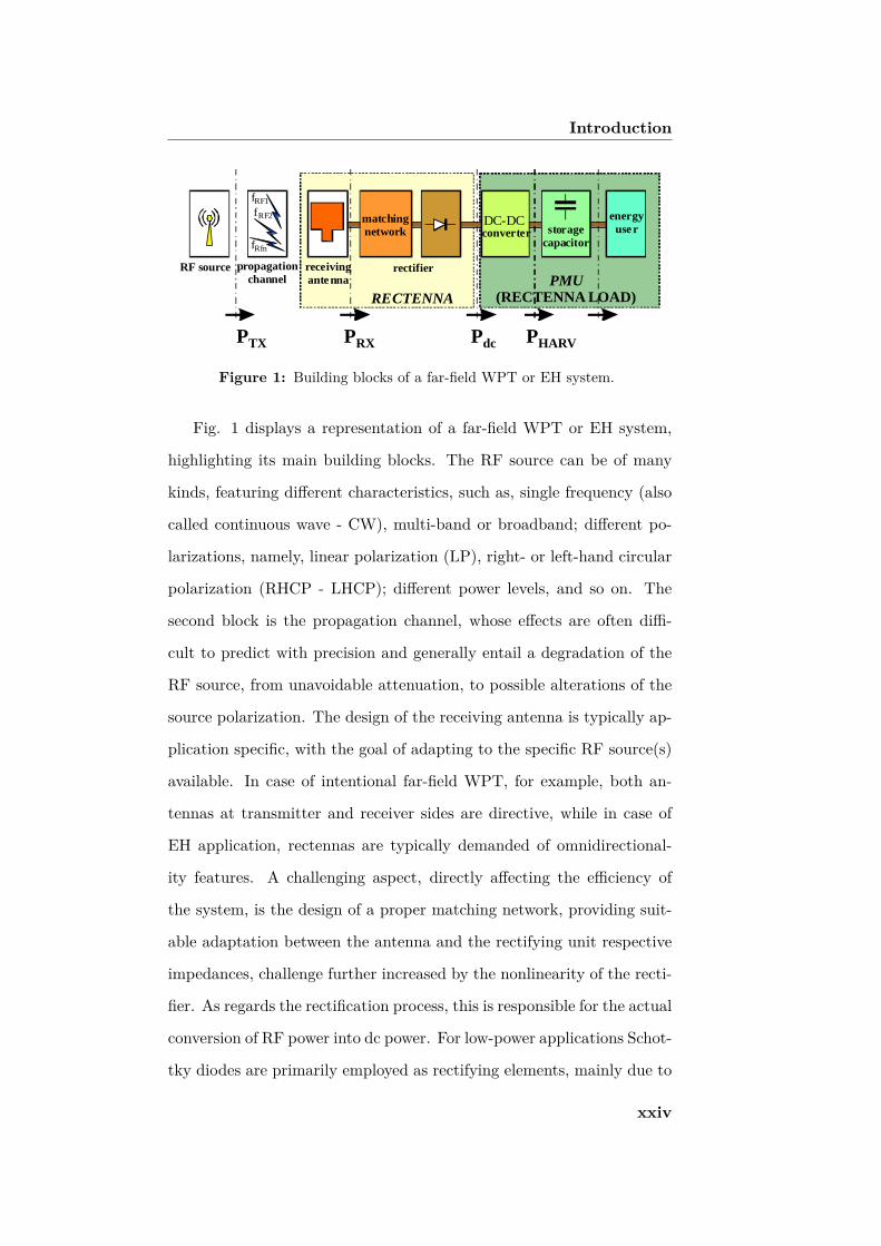
Figure 1: Building blocks of a far-field WPT or EH system.
Fig. 1 displays a representation of a far-field WPT or EH system,
highlighting its main building blocks. The RF source can be of many
kinds, featuring different characteristics, such as, single frequency (also
called continuous wave - CW), multi-band or broadband; different po-
larizations, namely, linear polarization (LP), right- or left-hand circular
polarization (RHCP - LHCP); different power levels, and so on. The
second block is the propagation channel, whose effects are often diffi-
cult to predict with precision and generally entail a degradation of the
RF source, from unavoidable attenuation, to possible alterations of the
source polarization. The design of the receiving antenna is typically ap-
plication specific, with the goal of adapting to the specific RF source(s)
available. In case of intentional far-field WPT, for example, both an-
tennas at transmitter and receiver sides are directive, while in case of
EH application, rectennas are typically demanded of omnidirectional-
ity features. A challenging aspect, directly affecting the efficiency of
the system, is the design of a proper matching network, providing suit-
able adaptation between the antenna and the rectifying unit respective
impedances, challenge further increased by the nonlinearity of the recti-
fier. As regards the rectification process, this is responsible for the actual
conversion of RF power into dc power. For low-power applications Schot-
tky diodes are primarily employed as rectifying elements, mainly due to
xxiv

Introduction
their low threshold, and they can be arranged in different topologies,
such as half-wave, full-wave, voltage multiplication, and so on. Before
being delivered to the final user, the dc output of the rectenna is typically
processed by a power management unit (PMU), which can therefore be
considered as the reference load during the rectenna design. The PMU
is mainly composed by a dc-dc converter and a storage capacitor, which
preserves the harvested energy for its final consumption.
When talking about efficiency it is of critical importance specifying
which are the precise quantities that are being compared. The RF-to-dc
conversion efficiency is defined as:
ηRF−dc =Pdc
PRX(1)
that is, the ratio between the dc power at the output of the rectenna
versus the RF power received by the antenna and made therefore avail-
able at the input of the matching network (refer to Fig. 1). On the
other hand, dc-to-dc efficiency, defined as:
ηdc−dc =PHARV
Pdc(2)
always referring to Fig. 1, identifies merely the conversion efficiency
of the dc-dc converter contained in the PMU. In other cases dc-to-dc
efficiency can also be an evaluation of the whole system efficiency, start-
ing from the dc energy at the transmitter side, before its conversion into
RF, the transfer to the receiver and its subsequent re-conversion into dc
for the receiver load. Typically, this last definition is mainly embraced
in near-field WPT application.
Regardless the specific technique implemented, the objective of WPT
is to remove or eliminate all the power cables connected to electronics,
xxv

Introduction
but also to eliminate or at least reduce the needs of charging batteries
in electric devices. In particular, far-field WPT systems are expected
to be the solution to deploy battery-less distributed electronics that are
difficult and/or are in such a large quantities that battery replacement is
too costly or even unfeasible. In this case the use of wireless power trans-
mission techniques can be exploited to develop and foster the internet of
everything evolution. Indeed, among the countless possible applications
of EH and WPT, the Internet of Things (IoT) is most assuredly one
of them, especially for low power WPT. The Internet of Things refers
to uniquely identifiable objects (things) and their virtual representa-
tions in an Internet-like structure. It is expected to bring about massive
improvements in user experience and system efficiency. It will have a
transformational impact on all industries and re-shape business models
and industry configurations. An estimated 30 billion connected devices
will be deployed by 2020 [40] and the total IoT revenue is expected to
grow to $1.2 trillion in 2022. As a result, IoT services are expected
to be a key driver for growth in the telecommunication industry. In
an IoT-perspective, the precise geographic location of a thing will be a
strategic requisite [41]. Indeed, some things in the IoT will be sensors,
and sensor location is usually important [42]. Therefore, the combina-
tion of radiofrequency identification (RFID), real time locating systems
(RTLS) and sensor technologies will enable the Internet to observe, iden-
tify and understand the world without the limitations of human-entered
data [43]. Besides localization, sensing and all the possible implemented
features, a paramount prerequisite will be energy supply. Indeed, every
single device, or connected object, needs a certain amount of power to
operate. It is well known that the usage of batteries entails inherent dis-
advantages in many situations, such as unsuitability or impracticability
xxvi

Introduction
of their replacement, impact on environmental pollution and so on. It
is in these cases, especially for low-power mW applications [44, 45], that
EH and WPT find room for development.
Throughout the whole duration of my Ph.D. activity I have been
mainly dedicated to the design of new solutions for rectennas, envi-
sioned for EH and low-power WPT applications. The following Ph.D.
thesis is organized as follows: Chapter 1 describes the design of an eco-
compatible tag for simultaneous EH and communication, realized on
paper substrate, Chapter 2 introduces a new concept for simultaneous
wireless power and information transfer, for which an accurate model of
a Schottky diode has been derived, Chapter 3 describes novel solutions
for increasing the activation distance of an energy autonomous tag, and
finally Chapter 4 illustrates the design of a low-cost near-field WPT
system, envisioned for RFID applications.
xxvii

Chapter 1
Eco-Compatible Next
Generation RFID Tag
The evolution of the contemporary society and the developments of in-
formation technologies have driven the pervasive diffusion of wireless
systems in the environment. More specifically, new systems employing
a large number of spatially distributed low-cost nodes (tags) are be-
ing adopted in applications among heterogeneous fields such as logistics
(e.g., tracking of goods in supply and distribution chains), security (e.g.,
localization and tracking of authorized people and goods in areas under
surveillance), environmental monitoring, and health-care (e.g., moni-
toring of patients, medical or paramedical personnel, medicines, and
health-care equipment). In all these scenarios, tags are required to be
identifiable, localizable and capable of sensing physical quantities with
high accuracy: functionalities traditionally offered by separated wireless
technologies, such as RFID, wireless sensor network (WSN), and RTLS.
Indeed, the ultra high frequency (UHF) RFID second generation (Gen.
2) [46] proved its validity in numerous application fields but still does
not offer capabilities of localization with high resolution, nor low power
1

sensing functionalities [47]. RTLS systems present some examples in the
commercial world, but uniquely based on active devices (with battery)
and with no integrated sensors [48]. Finally, the WSN technology, as
RTLS, does not provide either zero-power characteristics by means of
backscatter transmission techniques or implementation of components
and circuits on eco-compatible materials [49]. Obviously, the possibility
to integrate all the aforementioned capabilities in a unique system, with
innovative and low-cost solutions, would tremendously extend the range
of applications. Moreover, the employed electronics should possess a
feature so far considered only marginally and usually ex post, but key
in the future: full compatibility with the environment.
Given these premises, the Italian national project GRETA (GREen
TAgs and sensors with ultra-wideband identification and localization ca-
pabilities) [50], was born to focus on the research of innovative solutions
and technologies aimed at the realization of a distributed system for
identification, localization, tracking and monitoring in indoor and out-
door scenarios, based on environmentally friendly materials. The main
goal is that of realizing tags which are:
• localizable with sub-meter precision even in indoor scenarios or in
presence of obstacles;
• small-sized (with an area in the order of a few square centimeters)
and lightweight;
• eco-compatible (i.e., made with recyclable materials);
• energy-autonomous (no batteries);
• low-cost to permit the employment of several tags in the applica-
tion scenario;
2

• capable of sensing physical quantities from the environment.
Specifically, to meet the requirements of low energy consumption and
high-localization precision ultra-wideband (UWB) techniques are ex-
ploited to efficiently transmit identification and positioning informa-
tion in backscattering from the tags towards the reader [51, 52]. These
schemes have been recently proposed and are growing of interest for the
unique capabilities of ensuring passive communication (i.e., without the
need of equipping the tag with an active transmitter) and high-resolution
ranging [53, 54, 55]. For this reason, UWB is adopted for the communica-
tion of data generated by the autonomous non-powered sensors. Besides
passive backscattering modulation, energy autonomy is reached by im-
plementation of energy harvesting techniques, together with ultra-low
power signal processing. Finally, eco-compatible recyclable materials
(e.g., paper, polyethylene terephthalate, etc.) are investigated for the
substrate of electronic circuits, to assure the “green electronics” feature.
1.0.1 Objectives and Potential Applications
In order to guarantee the correct functionalities of the distributed low
power intelligence (zero power smart tags), the GRETA system is de-
signed to rely on an infrastructure composed of cooperative radio nodes
(readers) able to perform real-time identification and tracking with sub-
meter resolution of tagged objects/persons. Moreover, besides the mere
scavenging of ambient RF power, the use of dedicated emitters, denoted
as “energy showers”, is also foreseen in the system scenario. The GRETA
system architecture is depicted in Fig. 1.1.
The study of these tags/sensors networks, combined with the em-
ployment of recyclable materials and energy harvesting systems, paves
the way to numerous applications, mainly oriented to the Internet of
3

Energy shower
Energy sources
Physical phenomena
reader
reader
reader
backscattered UWB signal
Interrogation UWB signal
Energy harvesting
Sensing
tag
tagtag
Figure 1.1: Representation of the GRETA system.
Things concept, some of which are also pointed out in the Horizon 2020
objectives. Among them:
• e-Health: energetically autonomous and not invasive sensors for
biomedical parameters (e.g., smart band-aids) or drugs monitoring
and in general for efficient hospital activities management;
• ICT for food: on-paper tags with embedded sensors for continuous
monitoring of the product along the production and commercial
distribution chain (e.g., cold chain).
• Factories of the future: goods tracking and monitoring along the
industrial process for an advanced logistic management (supply
chain management).
Further applications concern domotics (e.g., for temperature, moisture,
and presence sensors) and cultural heritage conservation (capillary, con-
tinuous, and non-invasive monitoring of the environmental conditions
near artworks in museums and galleries). Two possible application sce-
narios are further detailed hereafter.
Factories of the Future
The introduction of an advanced RFID network able to identify, moni-
tor, and track objects based on eco-compatible technology has the poten-
4

tial to revolutionize the way of producing, transporting and consuming
various goods, and its use is interesting in innumerable applications in
several areas of our daily life. Probably the deepest impact will be in
the logistics and related areas, which will benefit an increase in pro-
ductivity, costs and time saving. The achievable high level of precision
and the extremely low cost of UWB ecological tags (compared with ac-
tual active RTLS) can be exploited with great benefits for logistic. The
possibility to apply low cost tags to boxes, pallets, and other objects
inside factories, deposits, warehouses, and stores can introduce many
advantages. It will also enable to know the spatial and the temporal
coordinates of the different components of the manufacturing process.
This will increase the potential for efficient logistics and manufacturing.
With the “just-in-time” philosophy one will minimize the time compo-
nents and final products stay in stock. Furthermore, the same tags can
prevent robbery because they are also alarm activating. The presence of
tag with embedded sensors paves the way to continuous monitoring of
perishable goods which require a continuative check of the environmen-
tal parameters (e.g., temperature/moisture). Special automated guided
vehicles (AGVs), equipped with smart tags and able to move from the
manufacturing line to the warehouse, could pick up the right boxes/con-
tainers and move them to the right place in the manufacturing line. The
AGVs themselves could be guided, without the need of any fixed guid-
ance, using the real-time localization capability so that they would have
a high operative flexibility with respect to different working scenes. As-
suming that personnel is identifiable and localizable through the same
smart tags, active protection against the moving AGVs can be enabled.
Fig. 1.2 shows a possible scenario.
5

Figure 1.2: Example of GRETA potential application for logistics and indus-trial production chain.
e-Health: Smart Hospital
In this context the proposed eco-compatible technology lends itself to
various applications, able to enhance efficiency management and pa-
tients safety in hospitals. As an example, with reference to Fig. 1.3,
one could think of single-use “smart band-aid” with an integrated tem-
perature sensor (thermometer) in continuous contact with the skin of
the patient. In such a way, when interrogated, the temperature sensor
is already at the equilibrium temperature, so the measurement time is
only due to the wireless data communication (few ms), and the current
drawbacks of mercury or infrared thermometers, such as systematic er-
rors, long measurements duration, use of highly polluting substances,
and difficulties in applying to kids patients, will be eliminated. The lo-
calization characteristics of the proposed system would finally allow the
continuous tracking of drugs and equipment also maintaining a contin-
uous checking on environmental conditions. For example, the tracking
and monitoring of blood product fluid bags of human nature from pro-
duction phase (blood donor) to consumer phase (transfusion in a patient)
in order to reduce the risk in the clinical transfusion field. In this contest
the main parameter to guarantee the good quality of blood products is
the temperature.
6

1.1. System Architecture
inventorytracking
smart rooms
peopletracking
SMART
HOSPITAL
Energy showers
Tag + harvester
mobile assetstracking
inventorytracking
smart rooms
peopletracking
SMART
HOSPITAL
Energy showers
Tag + harvester
mobile assetstracking
inventorytracking
smart rooms
peopletracking
SMART
HOSPITAL
Energy showers
Tag + harvester
mobile assetstracking
inventorytracking
smart rooms
peopletracking
SMART
HOSPITAL
Energy showers
Tag + harvester
mobile assetstracking
Figure 1.3: Example of GRETA potential application for smart hospital.
1.1 System Architecture
The activity and outcomes contained in this thesis fall within the GRETA
project. Specifically, the presented part describes the design of the green
tag antenna: an innovative ad hoc antenna suitable for joint UWB-UHF
simultaneous backscatter communication and energy harvesting, featur-
ing a flat, low profile and compact size architecture. The design of the
RF electronics, integrated in the tag, is also detailed in the thesis. Cor-
rect functionalities and dual-band operation simultaneity are guaran-
teed by a diplexer network. This network provides matching conditions
for both operating bandwidths, as well as decoupling between them.
To comply with the small required dimensions, the diplexer network is
miniaturized. Connection between the antenna and the diplexer is also
described in details. Fig. 1.4 shows the GRETA system architecture,
where the part subject of this activity is highlighted.
Design details of the various part of the tag are described in the
following Sections, together with the corresponding performance. An
extensive illustration of the various prototypes realization is given, for
intermediates steps on FR-4 and Taconic substrates. Finally, in view of
7

1.2. Integrated UWB-UHF Antenna
Presented tag
energy
harvestingstorage
control
logic
UHF/UWB antenna
sensor
backscatter modulator
energy
UHF
demodulator
UHF
UWB
Diplexer- matching- filtering
Figure 1.4: Schematic representation of the GRETA tag architecture, wherethe highlighted area corresponds to the described design activity.
the eco-compatibility requirement, the whole tag is designed and realized
on paper substrate. Paper is indeed an excellent candidate to reduce
environmental impact of electronic circuits: it is widely available at a
very low cost and most of all its highly biodegradability, with respect to
other ceramic substrates, allows it to turn into organic matter in landfills
in only a few months [56].
1.2 Integrated UWB-UHF Antenna
UWB techniques, in the European lower UWB band from 3.1 to 4.8
GHz , are chosen for the communication and localization functionalities
thanks to their interference robustness characteristics, even in indoor
scenarios. Moreover, an additional benefit in adopting UWB commu-
nication is the ultra-low power consumption, which makes it possible
to deploy battery-less RFID sensors by exploiting RF energy harvest-
ing. For energy harvesting purposes, though, UWB technology is not
adoptable due to the allowed extremely low-spectral power density [57],
which does not make it a good candidate for efficient usage of nonlinear
devices, responsible for the RF-to-dc rectification.
8

1.2. Integrated UWB-UHF Antenna
0
100
200
300
400
500
600
700
800
900
1 2 3 4 5
Rec
tifi
ed p
ow
er (m
W)
distance (m)
900 MHz
2450 MHz
Figure 1.5: Modeled dc output power for two comparable rectennas, operatingat 900 and 2450 MHz.
A possible solution, to keep the same radiating element for both com-
munication and energy harvesting, could be the exploitation of the 2.45
GHz ISM band, which is close to the lower limit of the UWB band. How-
ever, this would limit the maximum reachable link distances, as clearly
shown in Fig. 1.5. This plot compares the rectified power delivered
to the optimum load of two rectennas operating at 900 and 2450 MHz,
versus the free-space distance from a fixed RF source. In both cases,
an effective radiated power (ERP) of 500 mW is employed, incident in
the maximum link direction. Both the antennas are connected to the
same full-wave rectifier through a suitable matching network [58]. The
great advantage in collecting RF energy from the ambient by exploiting
the UHF band is clear: roughly one order of magnitude less in terms of
rectified power is achieved at 2.45 GHz. Thus, the best solution appears
to be the combination of two radiating elements: one designed for en-
ergy harvesting purposes in the UHF band and the other one to sustain
UWB communication. Moreover, this choice has the great advantage of
guaranteeing possible compatibility with previous RFID generations, as
strongly recommended by market needs.
Combined UWB-UHF solutions have been recently investigated [59,
9

1.2. Integrated UWB-UHF Antenna
60, 61, 62], but most of them consist of optimized placement of separate
antennas with two different ports: one for UWB communication and
the other for UHF communication/harvesting. The presented activity
describes the first single-port antenna solution for hybrid UWB-UHF
operation. This results in a superior size reduction with respect to pre-
vious solutions, at the same time guaranteeing a high quality of the
radiation characteristics. Prior to the design of an eco-compatible tag
with recyclable materials, a first prototype of the proposed topology is
realized on a standard FR-4 substrate to validate design results.
1.2.1 Antenna Design
As in all wideband applications, an almost uniform antenna behavior
in the whole frequency band, from the near-field (antenna impedance)
and far-field points of view, is an important design requirement, though
not always satisfied by the available solutions. Moreover, circular po-
larization is desirable in RFID applications to reduce tag installation
constraints. A large number of wideband antennas are available from
literature. The simplest choice is to resort to step-wise [63] or tapered
[62, 64, 65] planar monopole topologies, with partial ground plane for
image theorem application, or similarly inspired solutions, such as the
Vivaldi antenna [65]. Many drawbacks pertain to these antennas: the
dispersive behavior in terms of both far- and near-field, the linear po-
larization of the radiated field, and the unbalanced nature of the port
(less suitable to chip connection). The antipodal Vivaldi antenna [66]
solves the problem of the unbalanced port, only. For the present de-
sign, we exploit the self-complementary architecture [67] which theo-
retically provides an almost constant port impedance behavior in the
whole band (ideal Z ≈ 188.5 Ω, practical Z ≈ 120 Ω, due to finite met-
10

1.2. Integrated UWB-UHF Antenna
alization thickness and feed line [67]) and identical radiation properties,
as a fixed-shape “active zone” moves along the structure, by varying
the operating frequency. Within this family of antennas, some topolog-
ical choices permit to satisfy the circular polarization constraint, too:
as the cases of standard Archimedean [67] and logarithmic spiral [65]
topologies, both providing a balanced port, or a tapered version of the
Archimedean spiral with unbalanced port [68]. The selected topology
for the present design is the Archimedean spiral, providing the minimum
size. This choice has been taken by comparison of EM simulations of
an Archimedean and a logarithmic spiral antenna printed on a 1.5 mm
thick FR-4 substrate (εr = 4.3, tan(δ) = 0.025 at 10 GHz), offering a
similar behavior.
Optimization of the Archimedean Spiral Antenna
A first coverage of the UWB band, from 3.1 up to 4.8 GHz, is obtained
by a 3.2-cm-diameter spiral, with lines width (equal to lines gap for the
autocomplementarity principle) of 1 mm. The “active zone” of this an-
tenna is the circular portion of the spiral having a circumference equal to
the working wavelength, λ: in this section, an in-phase condition for the
currents flowing in the two stripes is reached, thus providing a behavior
equivalent to a full-wavelength loop antenna [67]. It is well known that
superior performance is achieved by thin-arms spiral antenna: the ex-
ploitation of vertical metallic strips (i.e., strips lain on the thin thickness
side) allows to have much tighter turns: this way the number of strip
turns can be considerably increased and thus a purer spiral behavior can
be achieved [69]. A further goal, however, is to accomplish an additional
UHF band coverage by means of a unique, compact, planar structure.
As a first attempt in this direction, the above-described Archimedean
11

1.2. Integrated UWB-UHF Antenna
spiral can be used by simply increasing its dimension; however, this so-
lution requires a spiral diameter of almost 13 cm to reach good radiation
properties at the desired frequency, thus obtaining a total area incompat-
ible with almost all RFID applications. This result clearly points out
the necessity to investigate ad hoc solutions to obtain the demanded
goal within suitable overall dimensions. Antenna miniaturization has
always been of great interest in both commercial and military applica-
tions, therefore several techniques and guidelines have been proposed
in literature [70, 71]. A possible solution would be that of using high
dielectric constants [72] or even magneto-dielectric [73] materials, but
the final aim of realizing an eco-friendly device forces to discard these
possibilities. Hence, a different miniaturization solution is investigated,
the so-called “gap-loading” technique [74]: the inclusion of a capacitive
load (a 1-mm-circular stripe, placed 1-mm-far from the spiral) increases
the electrical length of the structure, thus reducing its overall dimension.
However, the almost 23% reduction factor reached is not yet enough for
the desired purpose.
Novel UWB-UHF Antennas Hybrid Topology
A new solution for co-localizing a UWB and a UHF antenna sharing
the same substrate and the same port can be obtained by extending the
spiral length to form a meandered dipole. In Fig. 1.6, the principle of the
presented idea is shown. The new topology justifies, from another point-
of-view, the choice of the Archimedean spiral, instead of the logarithmic
one: the fusion of the spiral with the dipole can be straightforwardly
obtained without any tapering in between the two structures. It is worth
noting that all the spiral paths contribute to the dipole antenna, thus
allowing an overall dipole length suitable for UHF band applications. It
12

1.2. Integrated UWB-UHF Antenna
UWB spiral
UHF dipole
x
y
x
y
z P=(x,y,z)q
f
Figure 1.6: Integrated UWB-UHF one-port antenna architecture.
must be stressed that the UHF dipole still offers linear polarization, as
standard straight dipoles: in fact, the far-field polarization is determined
by the vertical arms departing from the spiral, while the rest of the
branches mainly contribute as reactive loads. Linear polarization of the
UHF antenna is required by the wireless powering mechanism foreseen in
the National Project for which this antenna has been developed [50]: this
is based on a set of intentional, linearly polarized UHF sources cleverly
deployed in the ambient to provide the RF power on demand (“energy
showers”), compliant with the maximum EIRP emission in the European
UHF 868 MHz RFID band [75]. Conversely, circular polarization for the
UWB antenna is chosen for communication/ranging purposes, as usually
required in most RFID applications.
To preserve the autocomplementarity of the spiral and to minimize
lines coupling in the long path providing the dipole operation, wider lines
with respect to previous experiments are chosen: lines and gaps width
is set to 1.5 mm. This value has been chosen as a good compromise to
guarantee the best spiral and dipole coexistence. Indeed this width leads
to a total UHF dipole length of a 1.5-l UHF dipole, while preserving a
compact layout. Conversely, reduced width size better ensures the spi-
ral currents in-phase condition [69] (with the number of turns increased
accordingly, to preserve the outer circumference dimension). However,
13

1.2. Integrated UWB-UHF Antenna
-20
-15
-10
-5
0
-150-125-100-75-50-25
0255075
100125150
700 750 800 850 900 950 1000
Max r
eali
zed
gain
(d
Bi)
Im(Z
11)
(W
)
Frequency (MHz)
L = 0 mm
L = 5 mm
L = 10 mm
L = 15 mm
L = 20 mm
(a) (b)
L
L
Figure 1.7: (a) Final topology of the proposed antenna. (b) Reactance andmaximum realized gain as a function of the length of the dipole.
this choice directly lengthens the UWB spiral arms and forces the use of
a 2.5-l UHF dipole, as the whole spiral path contributes to the dipole
antenna. By EM simulation [76], it is proved that this configuration
worsens dipole performance, as most of its length comes from the spiral
path. As a consequence, its polarization is turned from perfectly linear
to elliptical. Moreover, longer and thinner paths involve higher losses,
which would be a critical aspect in view of an ultra-low power, eco-
compatible realization on recyclable substrate. Finally, a standard 0.5-l
dipole cannot be adopted as well, as it would require an excessive re-
duction of the number of turns at the expense of the spiral performance,
especially in the lower UWB frequency range.
The final topology of the antenna is reported in Fig. 1.7(a). The
folded dipole layout guarantees a resonant behavior at 868 MHz (imag-
inary part of the dipole impedance equal to zero). However, if the an-
tenna is used with a standard UHF-RFID chip (for compatibility pur-
poses with previous generations), an easy conjugate matching can be
obtained by varying the final part of the dipole length (L) of Fig. 1.7(a).
This is clearly shown in Fig. 1.7(b), where the imaginary part of the
dipole input impedance is plotted versus frequency, with L as a parame-
ter. It can be observed that a 20-mm length variation provides a 100 W
14

1.2. Integrated UWB-UHF Antenna
@ 868 MHz @ 3 GHz
@ 4 GHz @ 5 GHz
Figure 1.8: Full-wave simulation results in terms of surface current magnitudein the UHF and UWB bands.
reactance span. From Fig. 1.7(b), it is also clear that, for any selected
length value, the reactance slope with respect to frequency does not vary
significantly. This allows us to conclude that the operating UHF-RFID
bandwidth (conjugate matching conditions) can be guaranteed for many
different dipole lengths. In Fig. 1.7(b), the corresponding realized gain,
in resonant conditions, is also plotted: its almost flat behavior confirms
that, by varying the branch L of the total dipole length, the radiation
properties in the UHF band are not significantly degraded. Thus, these
tuning properties can be potentially exploited for compatibility with
standard RFID chips.
The first demonstration of the effectiveness of the presented idea is
reported in Fig. 1.8, where the surface current magnitude, computed by
full-wave simulation in correspondence to the operating frequencies, is
assessed. Besides the shift of the active zone within the UWB band, the
1.5-l behavior in the UHF band can be noticed, too: indeed two zero
current values for each branch are evident. A further confirmation of the
optimal coexistence of the two antennas is then provided by the highly
15

1.2. Integrated UWB-UHF Antenna
-50
-45
-40
-35
-30
-25
-20
-15
-10
-5
0
3000 3500 4000 4500 5000
|r| (d
B)
Frequency (MHz)
Integrated UWB-UHF antenna
Spiral
Figure 1.9: Antenna performance in terms of reflection coefficient, withoutdipole (gray line) and with dipole (black line).
similar spiral performance with and without the dipole. In Fig. 1.9, the
reflection coefficient (normalized to 120 W) is shown: a maximal value of
−10 dB is guaranteed for the two configurations in the frequency band of
interest. In Fig. 1.10, the plots of the radiation patterns in the yz-plane
(see Fig. 1.6) at the UWB center-frequency are compared, showing an
excellent agreement. The same is true for the antenna circular polar-
ization properties: in Fig. 1.11, the axial ratio (AR) in the xz- and
yz-planes of the UWB antennas is compared: a maximum difference of
1.5 dB is predicted in both planes. Similar results have been obtained
all over the 3− 5 GHz band, thus ensuring the proper UWB communi-
cation in the presence of the UHF dipole. Previous results also justify
the insensitivity of the UWB antenna near- and far-field properties to
dipole length variation, as verified by EM simulation.
1.2.2 Antenna Experimental Characterization
For a first, extended characterization of the new UWB–UHF integrated
antenna, the first prototype is realized on FR-4 substrate. The photo of
the prototype with the associated dimensions is shown in Fig. 1.12(a).
16

1.2. Integrated UWB-UHF Antenna
-10
-5
0
5
Integrated UWB-UHF antenna Spiral
Rea
lize
d G
ain
(d
Bi)
0
90
180
270
q
Figure 1.10: Antenna performance in terms of realized gain in the yz-planeat the central UWB band frequency of 4 GHz, without dipole (gray line) andwith dipole (black line).
0
5
10
15
20
25
30
-90 -60 -30 0 30 60 90
AR
(d
B)
q ( )
Integrated UWB-UHF antenna yz plane
Spiral yz plane
Integrated UWB-UHF antenna xz plane
Spiral xz plane
Figure 1.11: Antenna simulated axial ratio at the central UWB band fre-quency of 4 GHz, with and without dipole, in the yz- and xz-plane.
17

1.2. Integrated UWB-UHF Antenna
31 mm
43 mm
1.5 mm
31 mm
43 mm
1.5 mm
(a) (b)
(a) (b)
Figure 1.12: Photo of the FR-4-based prototype: (a) front view and (b)perspective view with the coaxial cable used in radiation pattern measurements.
As regards antenna port measurements, the interface between the unbal-
anced measurement equipment and the balanced nature of the antenna
port has to be considered. A possible approach can be resorting to
the measurement procedure proposed in [77], where a Y-shaped three-
ports coaxial junction is used. After applying the cable de-embedding
procedure, an excellent correspondence between measured and modeled
antenna impedance is obtained, shown in Fig. 1.13, spanning both the
UHF and UWB bands. From inspection of the figure, the exact reso-
nance at 868 MHz, and the almost constant behavior in the UWB band
can be easily evinced; the third zero-crossing of the reactance in the lower
band clearly confirms that the total length of the dipole provides a 1.5-l
behavior. It can be observed that in the UHF band, the integrated an-
tenna shows an impedance real part of about 12 W, which is acceptable
for efficient matching to an RF-to-dc rectifier. These results also show
that the real part of the impedance is of only few W in correspondence
of the first zero-crossing of the reactance, which further confirms that
a common half-wavelength topology would not be convenient due to its
extremely low resistance values.
18

1.2. Integrated UWB-UHF Antenna
60
80
100
120
140
160
180
200
3000 3500 4000 4500 5000
Re(
Z)
(W)
Frequency (MHz)
0
200
400
600
800
1000
250 750 1250 1750
Re(
Z)
(W)
Frequency (MHz)
-20
0
20
40
60
80
100
3000 3500 4000 4500 5000
Im(Z
) (W
)
Frequency (MHz)
-1000
-750
-500
-250
0
250
500
750
1000
250 750 1250 1750
Im(Z
) (W
)
Frequency (MHz)
(a) (b)
(c)
(d)
modelled
measured
Figure 1.13: Measured and modeled antenna input impedance: (a) real part;(b) imaginary part in the UHF band; (c) real part; and (d) imaginary part inthe UWB band.
Very good agreement can also be observed by comparison of the
modeled and measured reflection coefficients in both the UHF and UWB
bands, by resorting to the proper normalization, as shown in Figs. 1.14
and 1.15, respectively.
Antenna far-field measurements are carried out in a real-office sce-
nario, and not in an anechoic chamber, to test the antenna performance
in practical applications. As we look for normalized behavior of the ra-
diation properties, direct connection of the conductors of a 50-W coaxial
cable [78, 79] to the antenna differential port is adopted in this case.
In Fig. 1.16, the predicted and measured radiation patterns of the co-
polarized and cross-polarized components in the E and H-plane (yz- and
xz-plane, respectively) of the UWB–UHF antenna at 868 MHz are re-
ported. As can be evinced, they prove to be almost identical to those
obtained by a standard straight standalone dipole. The unique differ-
19

1.2. Integrated UWB-UHF Antenna
-20
-15
-10
-5
0
200 400 600 800 1000 1200 1400 1600
|r| (d
B)
Frequency (MHz)
modelled measured
-20
-15
-10
-5
0
800 850 900 950
889 MHz854 MHz
Figure 1.14: Measured and modeled reflection coefficient in the UHF band(normalized to 12 W). 0.5-l, 1.5-l, and 2.5-l resonances can also be recognized.
-50
-40
-30
-20
-10
0
3000 3500 4000 4500 5000
|r| (d
B)
Frequency (MHz)
modelled measured
Figure 1.15: Measured and modeled reflection coefficient in the UWB band(normalized to 120 W).
20

1.2. Integrated UWB-UHF Antenna
-30
-25
-20
-15
-10
-5
0
No
rma
lize
d E
(d
B)
0
90
180
270
q
No
rma
lize
d E
(d
B)
0
90
180
270
q
No
rma
lize
d E
(d
B)
0
90
180
270
q
No
rma
lize
d E
(d
B)
0
90
180
270
q
No
rma
lize
d E
(d
B)
0
90
180
270
q
No
rma
lize
d E
(d
B)
0
90
180
270
q
No
rma
lize
d E
(d
B)
0
90
180
270
q
No
rma
lize
d E
(d
B)
0
90
180
270
q
No
rma
lize
d E
(d
B)
0
90
180
270
q
No
rma
lize
d E
(d
B)
0
90
180
270
q
No
rma
lize
d E
(d
B)
0
90
180
270
q
No
rma
lize
d E
(d
B)
0
90
180
270
q
No
rma
lize
d E
(d
B)
0
90
180
270
q
No
rma
lize
d E
(d
B)
0
90
180
270
q
No
rma
lize
d E
(d
B)
0
90
180
270
q
No
rma
lize
d E
(d
B)
0
90
180
270
q
No
rma
lize
d E
(d
B)
0
90
180
270
q
No
rma
lize
d E
(d
B)
0
90
180
270
q
No
rma
lize
d E
(d
B)
0
90
180
270
q
No
rma
lize
d E
(d
B)
0
90
180
270
q 0
90
180
270
q 0
90
180
270
q 0
90
180
270
q 0
90
180
270
q
N
0
90
180
270
q 0
90
180
270
q 0
90
180
270
q 0
90
180
270
q 0
90
180
270
q 0
90270
q 0
90270
q 0
90
180
270
q
-30
-25
-20
-15
-10
-5
0
No
rma
lize
d E
(d
B)
0
90
180
270
q
No
rma
lize
d E
(d
B)
0
90
180
270
q
No
rma
lize
d E
(d
B)
0
90
180
270
q
No
rma
lize
d E
(d
B)
0
90
180
270
q
No
rma
lize
d E
(d
B)
0
90
180
270
q
No
rma
lize
d E
(d
B)
0
90
180
270
q
No
rma
lize
d E
(d
B)
0
90
180
270
q
No
rma
lize
d E
(d
B)
0
90
180
270
q
No
rma
lize
d E
(d
B)
0
90
180
270
q
No
rma
lize
d E
(d
B)
0
90
180
270
q
No
rma
lize
d E
(d
B)
0
90
180
270
q
No
rma
lize
d E
(d
B)
0
90
180
270
q
No
rma
lize
d E
(d
B)
0
90
180
270
q
No
rma
lize
d E
(d
B)
0
90
180
270
q
No
rma
lize
d E
(d
B)
0
90
180
270
q
No
rma
lize
d E
(d
B)
0
90
180
270
q
No
rma
lize
d E
(d
B)
0
90
180
270
q
No
rma
lize
d E
(d
B)
0
90
180
270
q
No
rma
lize
d E
(d
B)
0
90
180
270
q
No
rma
lize
d E
(d
B)
0
90
180
270
q
No
rma
lize
d E
(d
B)
0
90
180
270
q
No
rma
lize
d E
(d
B)
0
90
180
270
q
No
rma
lize
d E
(d
B)
0
90
180
270
q
No
rma
lize
d E
(d
B)
0
90
180
270
q
No
rma
lize
d E
(d
B)
0
90
180
270
q
No
rma
lize
d E
(d
B)
0
90
180
270
q
No
rma
lize
d E
(d
B)
0
90
180
270
q
No
rma
lize
d E
(d
B)
0
90
180
270
q
No
rma
lize
d E
(d
B)
0
90
180
270
q
No
rma
lize
d E
(d
B)
0
90
180
270
q
No
rma
lize
d E
(d
B)
0
90
180
270
q
No
rma
lize
d E
(d
B)
0
90
180
270
q
No
rma
lize
d E
(d
B)
0
90
180
270
q
No
rma
lize
d E
(d
B)
0
90
180
270
q
No
rma
lize
d E
(d
B)
0
90
180
270
q
No
rma
lize
d E
(d
B)
0
90
180
270
q
No
rma
lize
d E
(d
B)
0
90
180
270
q
No
rma
lize
d E
(d
B)
0
90
180
270
q
No
rma
lize
d E
(d
B)
0
90
180
270
q
No
rma
lize
d E
(d
B)
0
90
180
270
q
No
rma
lize
d E
(d
B)
0
90
180
270
q
No
rma
lize
d E
(d
B)
0
90
180
270
q
No
rma
lize
d E
(d
B)
0
90
180
270
q
No
rma
lize
d E
(d
B)
0
90
180
270
q
No
rma
lize
d E
(d
B)
0
90
180
270
q
No
rma
lize
d E
(d
B)
0
90
180
270
q
No
rma
lize
d E
(d
B)
0
90
180
270
q
No
rma
lize
d E
(d
B)
0
90
180
270
q
No
rma
lize
d E
(d
B)
0
90
180
270
q
No
rma
lize
d E
(d
B)
0
90
180
270
q
No
rma
lize
d E
(d
B)
0
90
180
270
q
No
rma
lize
d E
(d
B)
0
90
180
270
q
No
rma
lize
d E
(d
B)
0
90
180
270
q
No
rma
lize
d E
(d
B)
0
90
180
270
q
No
rma
lize
d E
(d
B)
0
90
180
270
q
No
rma
lize
d E
(d
B)
0
90
180
270
q
No
rma
lize
d E
(d
B)
0
90
180
270
q
No
rma
lize
d E
(d
B)
0
90
180
270
q
No
rma
lize
d E
(d
B)
0
90
180
270
q
No
rma
lize
d E
(d
B)
0
90
180
270
q
No
rma
lize
d E
(d
B)
0
90
180
270
q
No
rma
lize
d E
(d
B)
0
90
180
270
q
No
rma
lize
d E
(d
B)
0
90
180
270
q
No
rma
lize
d E
(d
B)
0
90
180
270
q
No
rma
lize
d E
(d
B)
0
90
180
270
q
No
rma
lize
d E
(d
B)
0
90
180
270
q
No
rma
lize
d E
(d
B)
0
90
180
270
q
No
rma
lize
d E
(d
B)
0
90
180
270
q
No
rma
lize
d E
(d
B)
0
90
180
270
q
No
rma
lize
d E
(d
B)
0
90
180
270
q
No
rma
lize
d E
(d
B)
0
90
180
270
q
No
rma
lize
d E
(d
B)
0
90
180
270
q
No
rma
lize
d E
(d
B)
0
90
180
270
q
No
rma
lize
d E
(d
B)
0
90
180
270
q
No
rma
lize
d E
(d
B)
0
90
180
270
q
No
rma
lize
d E
(d
B)
0
90
180
270
q
No
rma
lize
d E
(d
B)
0
90
180
270
q
No
rma
lize
d E
(d
B)
0
90
180
270
q
No
rma
lize
d E
(d
B)
0
90
180
270
q
No
rma
lize
d E
(d
B)
0
90
180
270
q
No
rma
lize
d E
(d
B)
0
90
180
270
q
No
rma
lize
d E
(d
B)
0
90
180
270
q
No
rma
lize
d E
(d
B)
0
90
180
270
q
No
rma
lize
d E
(d
B)
0
90
180
270
q
No
rma
lize
d E
(d
B)
0
90
180
270
q
No
rma
lize
d E
(d
B)
0
90
180
270
q
No
rma
lize
d E
(d
B)
0
90
180
270
q
No
rma
lize
d E
(d
B)
0
90
180
270
q
No
rma
lize
d E
(d
B)
0
90
180
270
q
No
rma
lize
d E
(d
B)
0
90
180
270
q
No
rma
lize
d E
(d
B)
0
90
180
270
q
No
rma
lize
d E
(d
B)
0
90
180
270
q
No
rma
lize
d E
(d
B)
0
90
180
270
q
No
rma
lize
d E
(d
B)
0
90
180
270
q
No
rma
lize
d E
(d
B)
0
90
180
270
q
No
rma
lize
d E
(d
B)
0
90
180
270
q
No
rma
lize
d E
(d
B)
0
90
180
270
q
No
rma
lize
d E
(d
B)
0
90
180
270
q
No
rma
lize
d E
(d
B)
0
90
180
270
q
No
rma
lize
d E
(d
B)
0
90
180
270
q
No
rma
lize
d E
(d
B)
0
90
180
270
q
No
rma
lize
d E
(d
B)
0
90
180
270
q
No
rma
lize
d E
(d
B)
0
90
180
270
q
No
rma
lize
d E
(d
B)
0
90
180
270
q
No
rma
lize
d E
(d
B)
0
90
180
270
q
No
rma
lize
d E
(d
B)
0
90
180
270
q
No
rma
lize
d E
(d
B)
0
90
180
270
q
No
rma
lize
d E
(d
B)
0
90
180
270
q
No
rma
lize
d E
(d
B)
0
90
180
270
q
No
rma
lize
d E
(d
B)
0
90
180
270
q
No
rma
lize
d E
(d
B)
0
90
180
270
q
No
rma
lize
d E
(d
B)
0
90
180
270
q
No
rma
lize
d E
(d
B)
0
90
180
270
q
No
rma
lize
d E
(d
B)
0
90
180
270
q
No
rma
lize
d E
(d
B)
0
90
180
270
q
No
rma
lize
d E
(d
B)
0
90
180
270
q
No
rma
lize
d E
(d
B)
0
90
180
270
q
No
rma
lize
d E
(d
B)
0
90
180
270
q
No
rma
lize
d E
(d
B)
0
90
180
270
q
No
rma
lize
d E
(d
B)
0
90
180
270
q
No
rma
lize
d E
(d
B)
0
90
180
270
q
No
rma
lize
d E
(d
B)
0
90
180
270
q
No
rma
lize
d E
(d
B)
0
90
180
270
q
No
rma
lize
d E
(d
B)
0
90
180
270
q
No
rma
lize
d E
(d
B)
0
90
180
270
q
No
rma
lize
d E
(d
B)
0
90
180
270
q
No
rma
lize
d E
(d
B)
0
90
180
270
q
No
rma
lize
d E
(d
B)
0
90
180
270
q
(dB
)
modelled Co-pol
measured Co-pol
modelled X-pol
measured X-pol
Figure 1.16: Measured and modeled normalized field radiation patterns ofthe co- and cross-polarized component at 868 MHz, in the (a) E-plane (yz) and(b) H-plane (xz) of the dipole.
ence with respect to a straight dipole is the absence of secondary lobes,
despite the geometrical 1.5-l length, as most of its total length is ar-
ranged in a spiral-like configuration. As regards, the polarization of the
dipole far-field, it results linearly polarized in the y-direction (main axis
of the dipole) for a wide elevation range. The slight asymmetry of the
radiation patterns of Fig. 1.16 is due to the coaxial cable termination
shown in Fig. 1.12(b), which is taken into account in the simulation,
too.
Similar conclusions can be drawn in the UWB band: Fig. 1.17 re-
ports the simulated and measured radiation patterns at the UWB-band
frequencies 3, 4, and 5 GHz, for both the co- and the cross-polarized
components. Due to the ungrounded antenna structure, in the z > 0
half-space, the co-polarized component is the right-handed circularly
polarized (RHCP) one, while in the z < 0 half-space (light gray area
in the figure), the co-polarized component is the left-handed circularly
polarized (LHCP) one. The coaxial cable junction in the back of the an-
tenna is the main reason of a non-negligible cross-polarized component,
as verified by simulation, too, and consequently of an AR worsening
with respect to the isolated antenna results of Fig. 1.11. The simu-
lated realized gain in the maximal radiation direction of the antenna is
21
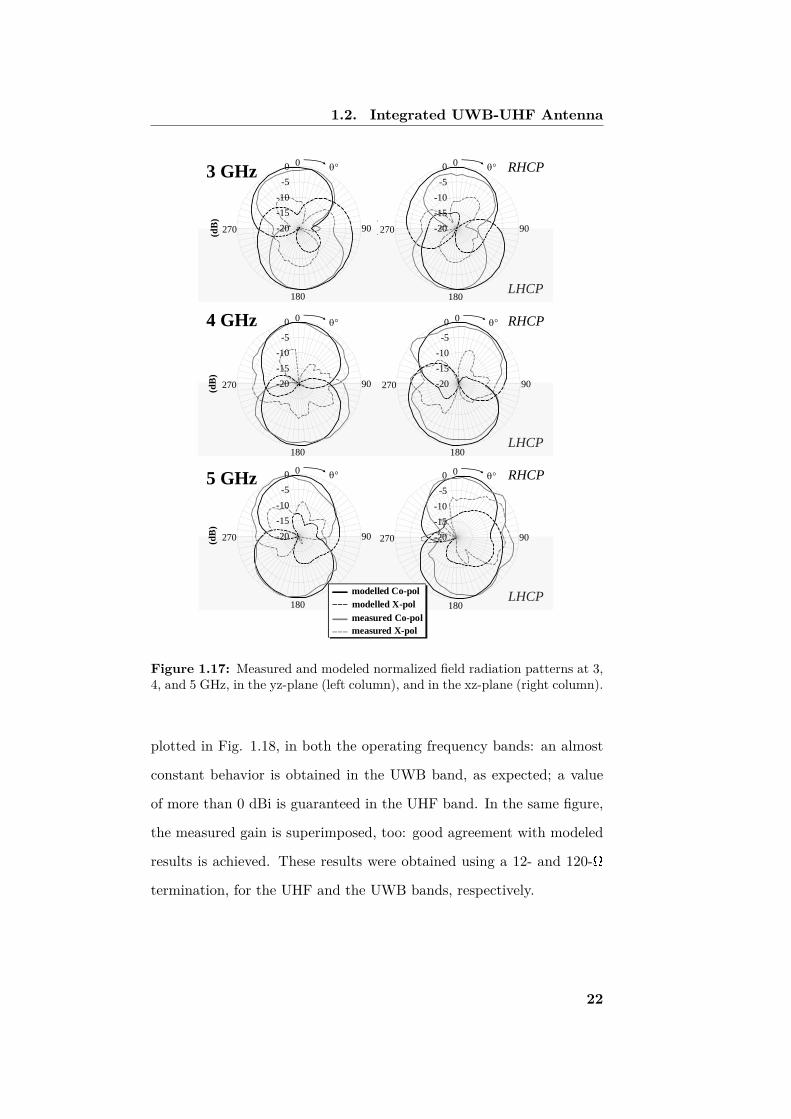
1.2. Integrated UWB-UHF Antenna
RHCP
LHCP
3 GHz
4 GHz
5 GHz
-20
-15
-10
-5
0
(dB
)
0
90
180
270
q
RHCP
LHCP
RHCP
LHCP
-20
-15
-10
-5
0
(dB
)
0
90
180
270
q
-20
-15
-10
-5
0
(dB
)
0
90
180
270
q
-20
-15
-10
-5
0
(dB
)
0
90
180
270
q
-20
-15
-10
-5
0
(dB
)
0
90
180
270
q
modelled Co-pol
measured Co-pol
modelled X-pol
measured X-pol
-20
-15
-10
-5
0
(dB
)
0
90
180
270
q
Figure 1.17: Measured and modeled normalized field radiation patterns at 3,4, and 5 GHz, in the yz-plane (left column), and in the xz-plane (right column).
plotted in Fig. 1.18, in both the operating frequency bands: an almost
constant behavior is obtained in the UWB band, as expected; a value
of more than 0 dBi is guaranteed in the UHF band. In the same figure,
the measured gain is superimposed, too: good agreement with modeled
results is achieved. These results were obtained using a 12- and 120-W
termination, for the UHF and the UWB bands, respectively.
22

1.3. Diplexer Network
-14
-12
-10
-8
-6
-4
-2
0
2
750 1000 1250 1500
Rea
lize
d G
ain
(d
Bi)
Frequency (MHz)
0
1
2
3
4
5
3000 4000 5000
Rea
lize
d G
ain
(d
Bi)
Frequency (MHz)
(a) (b)
Figure 1.18: Simulated (solid line) and measured (markers) realized gain ofthe FR4-prototype in the (a) UHF band and (b) UWB band.
1.3 Diplexer Network
The co-localization of the two radiating elements leads to a single-port
antenna architecture. This situation can be remarkably advantageous
for the direct connection of a single chip, located in the center part of
the antenna, which embeds the whole tag circuitry. For a hybrid pro-
totype realization, though, a proper three-way matching network needs
to be accurately designed. This network, or diplexer, is a three-port
microstrip/lumped element antenna-feeding network able to simultane-
ously provide high decoupling between the UHF and the UWB paths as
well as their respective matching conditions. In particular, the diplexer
is designed to connect the antenna (port 1) to a rectifier for the UHF
path (port 2), and a UWB modulator for the UWB path (port 3). This
simultaneously guarantees decoupling and matching conditions for both
the UHF and the UWB paths, by means of a lumped elements filter in
the UHF band, and a microstrip filter in the UWB band. The challeng-
ing aspect is to reach these goals with reduced dimensions in order not
to affect the antenna performance. In view of a unique UWB-UHF chip
realization, the diplexer network can be used as a proof-of-concept to be
integrated in a unique chip. Different aspects need to be simultaneously
23

1.3. Diplexer Network
Port 2
Figure 1.19: Schematic of the diplexer circuit topology. Port 2 is an artificialtermination introduced for evaluation of the diplexer performance.
accounted for in this feeding network design, namely:
1. preserving the radiating performance of the ungrounded antenna;
2. realizing a suitable transition from the antenna balanced port to
the unbalanced microstrip network;
3. separating and matching the UHF and UWB paths with minimum
insertion losses.
Fig. 1.19 illustrates the diplexer topology. In the UHF band, the
diplexer is responsible for filtering the signal as well as providing match-
ing condition towards the following rectifier, which converts the RF in-
coming signal into dc output power. This filter is realized with lumped
SMD components. For the rectifying section a full-wave voltage-doubler
topology, exploiting Schottky diodes SMS7630-079LF from Skyworks
[80], has been adopted. As regards the UWB band, the communica-
tion capabilities are provided by the exploitation of passive backscat-
tering; therefore the UWB port of the diplexer will be connected to a
backscatter modulator, which will be responsible for the modulation of
the incoming signal by switching its impedance between the two mis-
24

1.3. Diplexer Network
-40
-35
-30
-25
-20
-25
-20
-15
-10
-5
0
800 830 860 890 920 950
(dB
)
Frequency (MHz)
S11 S21 S23
-45
-40
-35
-30
-25
-20
-25
-20
-15
-10
-5
0
2400 2800 3200 3600 4000 4400 4800
(dB
)
Frequency (MHz)
S11 S31 S23
(a) (b)
Figure 1.20: Simulated scattering parameters of the three-port network ofFig. 1.19 in the (a) UHF band and (b) UWB band.
matched conditions of open and short circuit terminations. For design
purposes, the UWB path of the diplexer has been matched to a 50 W
termination; nevertheless a similar design procedure can be successfully
followed for any other loading conditions. The UWB path is realized
with a distributed element filter, composed by a microstrip line featur-
ing two short-circuited stubs.
Nonlinear/electromagnetic co-simulation [81] is then adopted to op-
timize the network for the stringent design goals described earlier. In
order to test the feasibility of the diplexer performance in view of an
eco-compatible substrate realization, the network is designed on a 0.69
mm thick paper substrate (εr = 2.85, tan(δ) = 0.053 at 4 GHz). The
simulated three-port circuit behavior is reported in Fig. 1.20, in terms
of scattering-parameter amplitudes: in this case, a complex impedance
of 20− j250Ω is used as the UHF port impedance (port 2 of Fig. 1.19).
This constant value has to be understood as the mean-value of the vari-
able nonlinear rectifier input impedance at the expected low input power
levels (from −20 to 0 dBm). For the present purpose, the UWB port
(port 3 of Fig. 1.19) has been kept referenced to 50Ω. The S21 and S31
plots show promising values of the transmission coefficients between the
25

1.4. Taconic Implementation
antenna port and the UHF and UWB ports, respectively: they are equal
or greater than −2 dB in both cases and all over the bands of interests,
in spite of the high paper losses.
The effectiveness of the designed network is also confirmed by the
high decoupling between the UHF and the UWB ports all over the bands
[see S23 in Figs. 1.20(a) and (b)]. Indeed, in order to successfully pro-
vide the demanded functionalities during all tag’s operating conditions,
the highest decoupling behavior between the UHF and the UWB fre-
quency bands is mandatory. For this reason a further inspection of the
diplexer performance under different operating circumstances has been
conducted. During the UWB backscattering communication, the UWB
modulator switches its impedance from an open circuit to a short cir-
cuit condition: these extremely different loads values could affect UHF
behavior too, if not properly decoupled. Fig. 1.21 shows UHF filtering
and matching performance for all the UWB different operating condi-
tions; this result clearly shows how the high decoupling provided between
the two operating bands guarantees a correct UHF operation. On the
other side, rectifying operation in the UHF band could affect the UWB
communication, especially because of the nonlinearity introduced by the
rectifying section. For this purpose the insertion loss introduced by the
UWB microstrip path is evaluated for different levels of the incoming
RF signal incident in the UHF band, as depicted in Fig. 1.22. Once
again, high decoupling proves to be guaranteed, allowing completely
transparent operations between the two operating bands.
1.4 Taconic Implementation
Thanks to the promising results obtained with the first evaluations of
both the UWB-UHF antenna and the diplexer network, a complete tag
26

1.4. Taconic Implementation
-25
-20
-15
-10
-5
0
800 830 860 890 920 950(d
B)
Frequency (MHz)
S21 (50 Ω) S21 (SC) S21 (OC)
-12
-10
-8
-6
-4
-2
0
800 830 860 890 920 950
(dB
)
Frequency (MHz)
S11 (50 Ω) S11 (SC) S11 (OC)
-40
-35
-30
-25
-20
-25
-20
-15
-10
-5
0
800 830 860 890 920 950
(dB
)Frequency (MHz)
S11 S21 S23
-40
-35
-30
-25
-20
-25
-20
-15
-10
-5
0
800 830 860 890 920 950(d
B)
Frequency (MHz)
S11 S21 S23
0
-2
-4
-6
-8
-10
-12 -40
-35
-30
-25
-20
-25
-20
-15
-10
-5
0
800 830 860 890 920 950
(dB
)
Frequency (MHz)
S11 S21 S23
(a) (b)
Figure 1.21: Diplexer UHF (a) matching and (b) filtering performance dis-tortion during the UWB modulation (SC - Short Circuit, OC - Open Circuit).
-8
-7
-6
-5
-4
-3
-2
-1
0
2400 2800 3200 3600 4000 4400 4800
(dB
)
Frequency (MHz)
Pin = -10 dBm
Pin = 0 dBm
Pin = 10 dBm
-45
-40
-35
-30
-25
-20
-25
-20
-15
-10
-5
0
2400 2800 3200 3600 4000 4400 4800
(dB
)
Frequency (MHz)
S11 S31 S23
-8
-7
-6
-5
-4
-3
-2
-1
0
-12
-10
-8
-6
-4
-2
0
800 830 860 890 920 950
(dB
)
Frequency (MHz)
S11 (50 Ω) S11 (SC) S11 (OC)
Figure 1.22: Filter insertion loss in the UWB band for different incident UHFpower levels.
27

1.4. Taconic Implementation
31 mm
43 mm
1.5 mm
10 mm
Figure 1.23: Photo of the Taconic-based prototype with the correspondingdimensions. The highlighted part in the center part of the antenna representsthe diplexer area on the backside of the tag.
has been designed and realized on Taconic substrate.
First, the integrated UWB-UHF antenna presented in Section 1.2 is
designed over a 0.635-mm-thick Taconic RF60A substrate (εr = 6.15,
tan(δ) = 0.0028 at 10 GHz). A picture of the prototype, realized with
an in-house milling machine, is provided in Fig. 1.23, along with the
corresponding dimensions. Electromagnetic simulation results exhibit
very good radiating characteristics, similar to those obtained with the
FR-4 realization. In the UWB band the antenna impedance has an
almost constant value of 120 W throughout the whole band, while radia-
tion efficiency and realized gain are approximately equal to 95% and 3.5
dBi, respectively. In the UHF band the 1.5-l meandered dipole shows a
purely real impedance of approximately 5 W at 868 MHz. The radiation
efficiency is in this case of 82%, with a realized gain of 0 dBi.
As previously discussed, the significant dispersive behavior of the
presented antenna needs a proper matching network in order to work
correctly. The diplexer network, whose topology has been introduced
in Fig. 1.19, is responsible for both matching and filtering of the UHF
and UWB bands, as well as decoupling between the two. Since the
28

1.4. Taconic Implementation
adopted UWB-UHF antenna has no ground plane, its radiation pattern
is bi-directional, being equally distributed in both the z > 0 and the
z < 0 half-spaces, for the two operating bands. This means that the
presence of nearby circuitry metalization can highly deteriorate antenna
performance. Hence, for a practical implementation of the tag, several
diplexer topologies have been investigated, focusing on preserving the
radiating properties of the antenna while at the same time ensuring a
low-profile structure. This means that, as anticipated, the diplexer has
to be implemented with reduced dimensions.
Given these constraints, a 1−cm2 microstrip/lumped elements diplexer
has been designed on a 0.635 mm-thick Taconic RF-60A substrate, which
runs parallel to the antenna substrate. The area of the diplexer network
and its placement on the backside of the integrated UWB-UHF antenna
can be observed in Fig. 1.23. Increasing circuit dimensions would lead to
a degradation of the ungrounded antenna performance, especially for the
higher frequencies of the UWB band: for this reason a miniaturization
of the diplexer circuit is mandatory.
1.4.1 Antenna-Diplexer Connection
As anticipated, a future single chip realization, providing all the func-
tionalities of the described diplexer, and directly connected to the bal-
anced single port presented antenna, would lead to a very compact de-
vice. As a first hybrid implementation, though, the described diplexer
has to be exploited, and because of the ungrounded nature of the an-
tenna, its placement and connection need accurate consideration. In-
deed, the presence of a metallic plane on the backside of the spiral an-
tenna would strongly influence its radiation characteristics. This degra-
dation would arise for increased diplexer dimensions, especially at the
29

1.4. Taconic Implementation
higher frequencies, involving the inner part of the spiral. The implemen-
tation of a 1−cm2 circuit, at a distance of 5 mm from the antenna, proves
to be a good compromise, influencing antenna behavior only marginally,
in terms of both radiation patterns and polarization, all over the fre-
quency bands of interest.
The single port antenna presents balanced feeding lines, therefore the
connection with the unbalanced microstrip/lumped elements diplexer
will have to take this transition into account. For this purpose a 5
mm-long balanced line departing from the center of the spiral arms is
built over the same 0.635 mm-thick Taconic RF-60A substrate and is
placed orthogonally to the antenna and diplexer substrate, connecting
the radiating element and the matching/feeding network in a balun-free
transition [82, 83]. This connection is shown in Fig. 1.24 where the
antenna structure has been made transparent for clarification purpose;
the diplexer ground plane removal is also visible, allowing one conductor
of the balanced line to reach the “hot” microstrip line on the top layer
of the diplexer. Two holes have been realized in order to wedge in the
balanced line substrate, one on the diplexer substrate and the other one
on the antenna substrate; extra Taconic sidewalls have also been added
for support purpose.
1.4.2 Diplexer Layout and Performance
The layout of the implemented diplexer is shown in Fig. 1.25. It is
mainly composed of three sections: the microstrip UWB matching and
filtering circuit, the lumped elements UHF matching and filtering circuit
(L1 and C1), and the rectifying section. In order to realize the requested
topology on a 1−cm2 area, the 32.3 mm-long microstrip line composing
the UWB path has been meandered. As regards the UHF path and
30
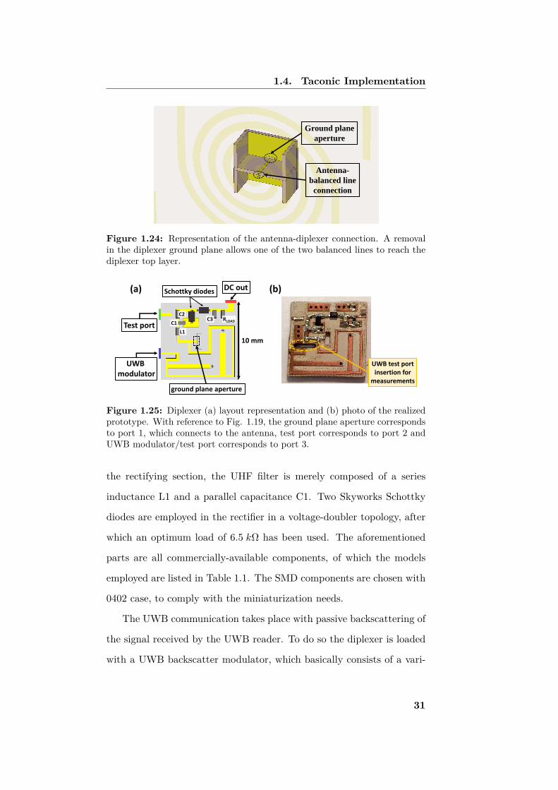
1.4. Taconic Implementation
Antenna-
balanced line
connection
Ground plane
aperture
Figure 1.24: Representation of the antenna-diplexer connection. A removalin the diplexer ground plane allows one of the two balanced lines to reach thediplexer top layer.
Schottky diodes
10 mm
DC out
Test port
UWB modulator
L1
C1
C2C3 RLOAD
(a) (b)
UWB test portinsertion for
measurementsground plane aperture
Figure 1.25: Diplexer (a) layout representation and (b) photo of the realizedprototype. With reference to Fig. 1.19, the ground plane aperture correspondsto port 1, which connects to the antenna, test port corresponds to port 2 andUWB modulator/test port corresponds to port 3.
the rectifying section, the UHF filter is merely composed of a series
inductance L1 and a parallel capacitance C1. Two Skyworks Schottky
diodes are employed in the rectifier in a voltage-doubler topology, after
which an optimum load of 6.5 kΩ has been used. The aforementioned
parts are all commercially-available components, of which the models
employed are listed in Table 1.1. The SMD components are chosen with
0402 case, to comply with the miniaturization needs.
The UWB communication takes place with passive backscattering of
the signal received by the UWB reader. To do so the diplexer is loaded
with a UWB backscatter modulator, which basically consists of a vari-
31

1.4. Taconic Implementation
Table 1.1: List of SMD components of the diplexer Taconic implementation.
Part name Manufacturer Product code Value
L1 Coilcraft 0402HP-15NXGLU 15 nH
C1 Murata GRM0225C1C1R5CD05D 1.5 pF
C2-C3 ATC 600L100FT200T 10 pF
D1-D2 Skyworks SMS7630-079LF
RLOAD Vishay CRCW04026K49FKED 6.5 kW
-45
-40
-35
-30
-25
-20
-15
-10
-5
0
0 1000 2000 3000 4000 5000 6000
(dB
)
Frequency (MHz)
S11 meas S11 sim S31 meas S31 sim
Figure 1.26: Comparison between the measured and simulated reflection andtransmission coefficient at ports 1 and 3 of the Taconic diplexer. Both portsare normalized on 50 W.
able impedance switching its value from OC to SC conditions. In order
to assess the diplexer performance in the UWB band, the scattering pa-
rameters at ports 1 and 3 are measured with a vector network analyzer
(VNA). The comparison between modeled and measured results is given
in Fig. 1.26. Despite an increased loss of 2-3 dB and a slight shrinkage in
the operating bandwidth, acceptable agreement is obtained. It is worth
noting that the simulated results are reported with a 50 W normalization
at both ports, to match with the measured one.
One of the requested tag functionalities is the simultaneous recovery
32
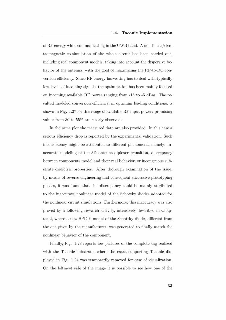
1.4. Taconic Implementation
of RF energy while communicating in the UWB band. A non-linear/elec-
tromagnetic co-simulation of the whole circuit has been carried out,
including real component models, taking into account the dispersive be-
havior of the antenna, with the goal of maximizing the RF-to-DC con-
version efficiency. Since RF energy harvesting has to deal with typically
low-levels of incoming signals, the optimization has been mainly focused
on incoming available RF power ranging from -15 to -5 dBm. The re-
sulted modeled conversion efficiency, in optimum loading conditions, is
shown in Fig. 1.27 for this range of available RF input power: promising
values from 30 to 55% are clearly observed.
In the same plot the measured data are also provided. In this case a
serious efficiency drop is reported by the experimental validation. Such
inconsistency might be attributed to different phenomena, namely: in-
accurate modeling of the 3D antenna-diplexer transition, discrepancy
between components model and their real behavior, or incongruous sub-
strate dielectric properties. After thorough examination of the issue,
by means of reverse engineering and consequent successive prototyping
phases, it was found that this discrepancy could be mainly attributed
to the inaccurate nonlinear model of the Schottky diodes adopted for
the nonlinear circuit simulations. Furthermore, this inaccuracy was also
proved by a following research activity, intensively described in Chap-
ter 2, where a new SPICE model of the Schottky diode, different from
the one given by the manufacturer, was generated to finally match the
nonlinear behavior of the component.
Finally, Fig. 1.28 reports few pictures of the complete tag realized
with the Taconic substrate, where the extra supporting Taconic dis-
played in Fig. 1.24 was temporarily removed for ease of visualization.
On the leftmost side of the image it is possible to see how one of the
33

1.5. Paper Implementation
0
10
20
30
40
50
60
-20 -15 -10 -5 0
Co
nv
ersi
on
eff
icie
ncy
(%
)
Available RF input power (dB)
modelled measured
Figure 1.27: RF-to-dc conversion efficiency for low levels of RF incomingavailable power. Inconsistent measured results are a consequence of the inac-curate manufacturer model of the Schottky diodes.
two balanced lines is modified at one end for connection to the diplexer
ground plane, in a balun-free transition. Whereas the rightmost part
shows the further 3D transition for insertion of the UWB port used dur-
ing the measurements, which has then to be replaced with the UWB
backscatter modulator.
1.5 Paper Implementation
In this Section the final implementation of the eco-compatible integrated
UWB-UHF tag is described. To fulfill the “green electronics” require-
ment the whole tag is designed and fabricated on paper. The tag fab-
rication, realized by the University of Perugia, partner of the GRETA
project, is based on conventional copper layer to be glued onto paper
sheets, which provides a possible alternative to the well-demonstrated
inkjet printing technology [84, 56, 85, 86, 87, 88]. Moreover, the proposed
low-profile paper layout guarantees eco-compatibility for more than 93%
of the total tag volume.
Since low-profile characteristics play a significant role as key enabler
34

1.5. Paper Implementation
43 mm 10 mm
5 mm
Figure 1.28: Pictures of the complete tag realized on Taconic substrate.
for a large number of applications, with respect to the architecture pre-
sented in Section 1.4, a new, more compact and mechanically stable
solution has been designed, allowing a total thickness of less than 1 mm.
To do so, the multilayer structure, shown in Fig. 1.29(a), is adopted,
with the goal of settling the low-profile and robustness requirements
with the lowest influence on antenna performance. Two paper sheets,
370 mm-thick, are used as the substrate for the antenna metalization
on the top and for the diplexer circuitry on the bottom, whose ground
plane is provided by inserting a 13.2x 13.2 mm2 flexible copper sheet,
0.3 mm-thick, between the two paper layers.
Antenna-diplexer connection is realized by means of two via-through
connecting one antenna arm to the diplexer ground plane, and the other
one to its input microstrip line. This way an effective balun-free transi-
tion between the unbalanced diplexer topology and the balanced antenna
port is realized. Fig. 1.29(b) shows a 3-D zoom of this connection, where
a squared slot of 2.2x 2.2 mm2 in the ground plane allows one arm of
the antenna to be connected to the microstrip. This solution does have
35
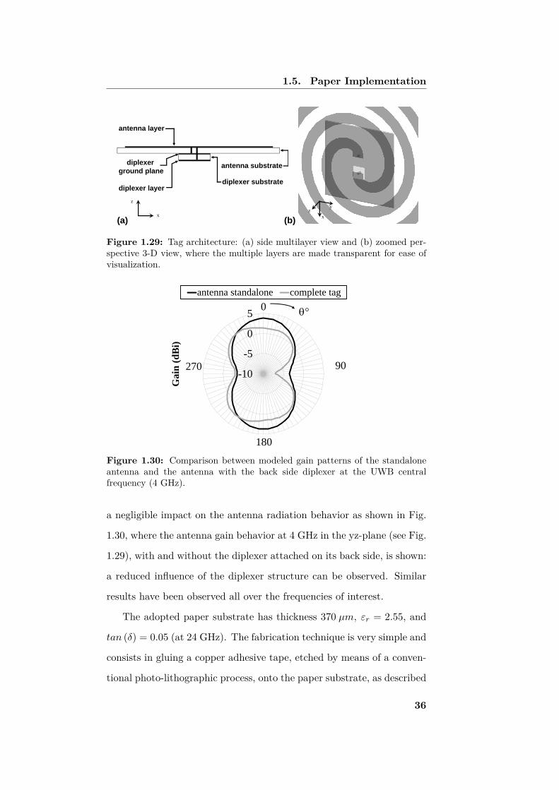
1.5. Paper Implementation
(a) (b)
diplexer
ground plane
antenna layer
antenna substrate
diplexer substratediplexer layer
x
zy
x
z
Figure 1.29: Tag architecture: (a) side multilayer view and (b) zoomed per-spective 3-D view, where the multiple layers are made transparent for ease ofvisualization.
-10
-5
0
5
antenna standalone complete tag
Gain
(d
Bi)
0
90
180
270
q
Figure 1.30: Comparison between modeled gain patterns of the standaloneantenna and the antenna with the back side diplexer at the UWB centralfrequency (4 GHz).
a negligible impact on the antenna radiation behavior as shown in Fig.
1.30, where the antenna gain behavior at 4 GHz in the yz-plane (see Fig.
1.29), with and without the diplexer attached on its back side, is shown:
a reduced influence of the diplexer structure can be observed. Similar
results have been observed all over the frequencies of interest.
The adopted paper substrate has thickness 370 µm, εr = 2.55, and
tan (δ) = 0.05 (at 24 GHz). The fabrication technique is very simple and
consists in gluing a copper adhesive tape, etched by means of a conven-
tional photo-lithographic process, onto the paper substrate, as described
36

1.5. Paper Implementation
49 mm
(a) (b)
x
y
z
1.9 mm
57 mm
Figure 1.31: (a) Integrated UWB-UHF antenna layout. (b) Prototype onpaper substrate.
in [89]. This procedure is employed for all the tag metalization layers.
Via-through junctions, which connect the antenna to the diplexer, have
been realized by means of copper wires with a diameter of 0.4 mm.
Fig. 1.31 reports the layout of the integrated UWB-UHF antenna. It
is worth noting that the frequency-dependent antenna-diplexer matching
is obtained with no need to refer to 50-W terminations, thus reducing
the needed circuitry between them and the associated losses [90, 91].
In Fig. 1.32 the measured and modeled antenna reflection coefficients
are reported, normalized to the 50-W termination of the instrument at
any operating frequency: a very good agreement is observed all over
the frequency band. With such unified normalization impedance for
any frequency, these plots do not directly provide the antenna operating
bandwidth, which would require a different normalization impedance
for each frequency point. As a representative result, Fig. 1.33, reports
the antenna input impedance in the UHF band, where the 868-MHz
resonance is clearly displayed.
The challenging requirements of the diplexer network are still appli-
cable. Indeed, it is simultaneously requested to be: i) miniaturized, to
ensure the low-profile of the entire tag; ii) inserted in such a way that
37
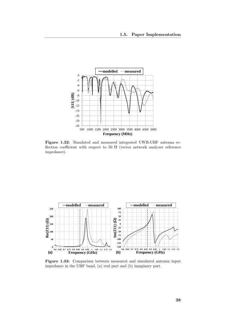
1.5. Paper Implementation
-20
-18
-16
-14
-12
-10
-8
-6
-4
-2
0
500 1000 1500 2000 2500 3000 3500 4000 4500 5000
|S11| (d
B)
Frequency (MHz)
modelled measured
Figure 1.32: Simulated and measured integrated UWB-UHF antenna re-flection coefficient with respect to 50 W (vector network analyzer referenceimpedance).
0
50
100
150
200
250
0.6 0.65 0.7 0.75 0.8 0.85 0.9 0.95 1 1.05 1.1 1.15 1.2
Re(
Z11
) (Ω
)
Frequency (GHz)
modelled measured
-150
-125
-100
-75
-50
-25
0
25
50
75
100
0.6 0.65 0.7 0.75 0.8 0.85 0.9 0.95 1 1.05 1.1 1.15 1.2
Im(Z
11
) (Ω
)
Frequency (GHz)
modelled measured
(a) (b)
Figure 1.33: Comparison between measured and simulated antenna inputimpedance in the UHF band, (a) real part and (b) imaginary part.
38

1.5. Paper Implementation
Schottky diodes
DC out
UWB port(to modulator)L1
C1
C2
C3RLOAD
13.2 mm
antenna port
(a) (b)
Figure 1.34: (a) Miniaturized diplexer layout, with area 13.2x 13.2mm2 andthickness 370 µm. (b) Picture of the prototype on paper substrate.
it does not perturb the antenna radiation characteristics; iii) able to
provide two paths: the UWB one, to be loaded by the backscattering
modulator, for localization and addressing; the UHF one to be loaded
by the rectifier for RF harvesting, with minima insertion losses in both
cases.
Once again, with reference to Fig. 1.19, the UWB branch consists of
a meandered two-stage microstrip filter, while the UHF one is based on
lumped element small SMD components (0402-case) and is connected
to a full-wave rectifier employing Schottky diodes. SMDs soldering has
been realized with the aid of conductive paste, at temperatures below
300° C, in order not to damage the paper substrate. The new layout of
the diplexer network on paper substrate is reported in Fig. 1.34. The
values and models of the UHF components are listed in Table 1.2.
1.5.1 Tag UHF Performance
Tag UHF harvesting capabilities are tested by connecting the diplexer
UHF output port to the rectifier. The RF-to-dc conversion efficiency is
the figure of merit to characterize the tag EH capabilities. The effective
RF received power is first measured using the antenna standalone, on a
50-W load, for a fixed distance and orientation of the transmitting UHF
39

1.5. Paper Implementation
Table 1.2: List of SMD components of the diplexer paper implementation.
Part name Manufacturer Product code Value
L1 Coilcraft 0402HP-18NXGLU 18 nH
C1 Murata GJM1555C1H1R0WB01D 1 pF
C2-C3 ATC 600L100FT200T 10 pF
D1-D2 Skyworks SMS7630-079LF
RLOAD Vishay CRCW04028K06FKED 8 kW
antenna. By taking into account the mismatch loss factor between the
instrument 50-W termination and the actual antenna impedance in the
UHF band, the available RF power at the diplexer input can be evalu-
ated. The measurement has been carried outside an anechoic chamber,
in different indoor scenarios, in order to realistically evaluate the RF
energy incidence at the tag locations. In a second step the reference
antenna is replaced with the entire tag for the same conditions of the
transmitting antenna and the dc rectifier output voltage is measured
on the optimized load (8 kΩ for the present design); the dc power is
computed accordingly.
The excellent comparison between the predicted EM-based nonlinear
results and the measured ones, in terms of RF-to-dc conversion efficiency,
are superimposed in Fig. 1.35, for a wide range of input RF power, from
-30 to 0 dBm. The corresponding rectified voltages on the optimum load
are also superimposed on the same plot. This test campaign, has been
repeated for all the possible loading conditions of the diplexer UWB
port (i.e., open-circuit, short-circuit or 50 W) to confirm the optimized
decoupling between the UHF and the UWB operations of the tag. For
an available input power as low as -10 dBm, the UWB-UHF tag is able
to provide a dc power of 44.8 mW and a dc voltage of 600 mV. Such
40

1.5. Paper Implementation
0
300
600
900
1200
1500
1800
2100
0
10
20
30
40
50
60
70
-30 -25 -20 -15 -10 -5 0
DC
Volt
age
(mV
)
Co
nv
ersi
on
eff
icie
ncy
(%
)
Available RF input power (dBm)
modelled measured
Figure 1.35: RF-to-dc conversion efficiency and rectified voltage on the opti-mum load for typically available RF input power levels.
quantities are well suitable to activate the ICs of the UWB path, for
localizing and addressing the paper tag [92].
For the present case the outcomes of the activity described in Chap-
ter 2 were exploited. Thanks to the new accurate SPICE model of the
Schottky diodes, capable of matching the nonlinear behavior of the com-
ponent, an excellent agreement was obtained.
1.5.2 Tag UWB Performance
Communication in the UWB band is carried out by passive backscat-
tering. For this reason, the diplexer UWB port will be connected to
a backscatter modulator. The modulation of the incident interrogation
signal can be implemented by a controlled switching of the UWB load
between the two conditions of open and short circuit terminations. For
the design of the diplexer, a reference 50 W load has been chosen. In this
way, when the tag is inactive, no reflections will occur from the tag if the
UWB port is terminated on a 50 W load (an equivalent design procedure
can be successfully followed for any other reference impedance).
The tag performance in the UWB band are first assessed in terms
41

1.5. Paper Implementation
0
5
10
15
20
25
30
35
40
0.5 1 1.5 2 2.5 3 3.5 4 4.5 5
(dB
)
Frequency (GHz)
modelled RL measured RL modelled IL measured IL
Figure 1.36: Comparison between measured and modeled diplexer antennaport return loss and antenna-to-UWB port insertion loss. Both UWB port andantenna port are referred to 50 W terminations.
of filtering and matching capabilities of the diplexer network. The scat-
tering parameters at ports 1 and 3 are measured with a vector network
analyzer (VNA). The measured and simulated insertion and return loss
are compared in Fig. 1.36, where the antenna port is replaced by the 50
W termination of the instrument.
Despite diplexer optimized miniaturization, because of the absence of
a ground plane, the antenna is influenced by the presence of the diplexer
metalization, as also reported by Fig. 1.30. Even though this influence
appears to be minor, it is worth evaluating to which extent it might affect
the communication capabilities of the tag. To do so, an accurate evalu-
ation of the system performance is carried out by means of circuit/EM
co-simulation. This procedure allows to predict in a straightforward way
the received UWB pulse spectrum and the associated contributions to its
amplitude and phase distortion for different tag configuration and differ-
ent TX-RX respective orientations. From the system point of view, this
information is fundamental, especially when time difference of arrival
(TDOA) techniques are adopted for localization purposes [93].
42

1.5. Paper Implementation
For the present case a linearly polarized UWB plane wave is cho-
sen as incident signal of the tag. According to the Harmonic Balance
(HB) principles the system excitation must be given in the frequency do-
main. The adopted UWB pulse waveform has duration and amplitude
dynamic designed to fit the European requirements [57], not exceed-
ing −41.3 dBm/MHz of transmitted EIRP in the 3.1-4.8 GHz band:
a fourth derivative of a Gaussian pulse with duration τd = 300 ps and
period TUWB = 6 ns is chosen. By the HB-based technique, such pulse
is accurately described by a fundamental frequency fUWB = 1/TUWB =
166MHz with NH = 64 harmonics: this way a wider frequency range
is retained in the HB analysis in order to accurately evaluate the effects
of nonlinear signal processing. The antenna is considered in receiving
mode. By resorting to EM theory [94, 95] a rigorous evaluation of the
pulse distortion at the antenna port can be carried out. The incident
linearly polarized UWB plane wave can be written as:
Ei (r;ωk) = Ei (r;ωk)(cosψθ + sinψφ
). (1.1)
In these conditions the equivalent Norton current generators are ob-
tained by combining 1.1 with the electric field the antenna would radiate
at a distance r and direction (θ, φ), in transmitting mode. In particular
the straightforward application of the reciprocity theorem to the trans-
mitted UWB pulse harmonics (Ei (r;ωk)) and the harmonics of the field
transmitted by the spiral antenna when powered by a voltage source
of known amplitude U and internal resistance R0 (EA (r;ωk)) allows
to evaluate the 64 equivalent Norton current generators needed for the
analysis, according to the following formula [96]:
43
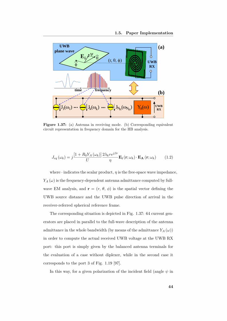
1.5. Paper Implementation
Ei
UWB
RX
(r, , )
UWB
plane wave
-1.50E+00
-1.00E+00
-5.00E-01
0.00E+00
5.00E-01
1.00E+00
1.50E+00
-1.50E-09 -1.30E-09 -1.10E-09 -9.00E-10 -7.00E-10 -5.00E-10 -3.00E-10 -1.00E-10
time-100
-90
-80
-70
-60
-50
-40
-30
-20
-10
0
0 1666666667 3333333333 5000000000 6666666667 8333333333 10000000000
frequency
J ( ) NH NHJ ( )k kJ ( )1 1
UWBRXAY ( )
(a)
(b)
Figure 1.37: (a) Antenna in receiving mode. (b) Corresponding equivalentcircuit representation in frequency domain for the HB analysis.
Jeq (ωk) = j[1 +R0YA (ωk)]
U
2λkrejβr
ηEi (r;ωk) ·EA (r;ωk) (1.2)
where · indicates the scalar product, η is the free-space wave impedance,
YA (ω) is the frequency-dependent antenna admittance computed by full-
wave EM analysis, and r = (r, θ, φ) is the spatial vector defining the
UWB source distance and the UWB pulse direction of arrival in the
receiver-referred spherical reference frame.
The corresponding situation is depicted in Fig. 1.37: 64 current gen-
erators are placed in parallel to the full-wave description of the antenna
admittance in the whole bandwidth (by means of the admittance YA (ω))
in order to compute the actual received UWB voltage at the UWB RX
port: this port is simply given by the balanced antenna terminals for
the evaluation of a case without diplexer, while in the second case it
corresponds to the port 3 of Fig. 1.19 [97].
In this way, for a given polarization of the incident field (angle ψ in
44

1.5. Paper Implementation
-0.6
-0.4
-0.2
0.0
0.2
0.4
2.5 3.0 3.5 4.0 4.5
E F
ield
(V
/m)
time (ns)
-3.0
-2.0
-1.0
0.0
1.0
2.0
3.0
2.5 3.0 3.5 4.0 4.5
UW
B R
X (
mV
)
time (ns)
θ = 0 θ = 10 θ = 20 θ = 30 θ = 40
-3.0
-2.0
-1.0
0.0
1.0
2.0
3.0
2.5 3.0 3.5 4.0 4.5
UW
B R
X (
mV
)
time (ns)
ψ = 0 ψ = 90
-3.0
-2.0
-1.0
0.0
1.0
2.0
3.0
2.5 3.0 3.5 4.0 4.5
UW
B R
X (
mV
)
time (ns)
w/o diplexer with diplexer
(b)
(a)
(c)
(d)
-3.0
-2.0
-1.0
0.0
1.0
2.0
3.0
3.00 3.05 3.10 3.15 3.20 3.25 3.30 3.35 3.40
UW
B R
X (
mV
)
time (ns)
θ = 0 θ = 10 θ = 20 θ = 30 θ = 40
Figure 1.38: Antenna distortion effects on the received pulse. (a) UWB pulseincident on the antenna. (b) Received pulse by the standalone antenna, for fixedpolarization (ψ = 0°) and varying incident elevation θ angle. (c) Received pulseby the standalone antenna, for fixed AOA and two different polarizations of theincident field. (d) Received pulse by the standalone antenna and the completetag with the diplexer.
45

1.5. Paper Implementation
Fig. 1.37), the procedure allows to predict the relationship between a
received pulse shape and its angle-of-arrival (AOA) and vice-versa. Fur-
thermore, the effect on distortion due to the antenna or to the antenna-
diplexer assembly are available as well, after the circuit-level analysis.
Comparison among transmitted (ideal) and received (real) pulses are
reported in Fig. 1.38. It is possible to notice that, besides amplitude
distortion, a certain phase delay is observed in all the cases. From Fig.
1.38(b) it is possible to see that different AOAs cause short delays, the
maximum one being 30 ps, reported for j = 10°. In this case the main
contribution for such distortion is due to the shape of the antenna ra-
diation pattern along that direction. Fig. 1.38(c) shows that a much
longer delay is obtained if the polarization of the incident UWB field is
rotated by 90°, and reaches 70 ps. Such contribution can be attributed
to slightly imperfect circular polarization provided by the antenna. Fi-
nally, Fig. 1.38(d) shows that the energy levels (defined as the difference
between the two received pulses areas over the pulse duration) at the
UWB RX port are comparable, which confirms that the presence of the
diplexer in the backside of the antenna does not weaken the UWB sys-
tem activity. From this figure it can also be noted that the presence
and absence of the diplexer introduces a 180° phase shift in the received
pulse. This last result is not detrimental, since such phenomenon is
commonly solved in practical UWB communication by means of a first
reference pulse of known polarity for each transmitted bit. Nevertheless
this behavior confirms the need for such a co-design technique to take
into account all these significant contributions in the evaluation of the
system performance. Moreover, it should be noted that in case of a
complete backscatter communication, all these delays are doubled.
The tag communication capabilities are finally experimentally vali-
46

1.5. Paper Implementation
Figure 1.39: UWB communication measurements in a real office scenario.
dated in a real environment, by setting up a scaled test-bed for the UWB
reader-tag system. The measurement setup is shown in Fig. 1.39. It
consists of an in-house quasi-monostatic linearly polarized UWB reader,
fed by an Arbitrary Wave Generator (AWG), with a pulse in this case
generated with a Root Raised Cosine centered at the UWB middle fre-
quency of 4 GHz, a pulse-width factor of 1 ns and roll-off factor 0.6
[98]. The AWG sequence of pulses is first amplified by a TX amplifier
and then delivered to the UWB reader antenna (a Vivaldi commercial
antenna was adopted). With a pulse repetition period set to 50 ns, 200
successive pulses are transmitted and subsequently received by the UWB
reader, which is the maximum acquisition window of the available oscil-
loscope at the receiver side. Such pulses redundancy allows increasing
the backscattered energy at the reader side and, therefore, the corre-
sponding Signal-to-Noise Ratio (SNR). Nevertheless, due to the limited
acquisition window of the oscilloscope, the transmitted power was in-
creased with the TX amplifier above the spectral mask limit, with a
47

1.5. Paper Implementation
(depends on the tag load)
y
zz
y
x
rf
t
Jtr
Z L
READER
1
backscatter signal (clutter)
TAG
CLUTTER
a (f)
b (f)
1
tag reference systemreader reference system
f
J
structural mode scattering
antenna mode scattering
x
backscatter signal (clutter)
SCATTERER
antenna mode scattering
(depends on ZL)
structural mode scattering
Figure 1.40: Representation of a passive backscattering communication,showing all the distinct signal components: clutter, tag structural mode andtag antenna mode (the only one dependent on the information).
power spectral density of about 25 dB over the −41.3 dBm/MHz limit.
The received backscattered signal at the reader side is captured by the
UWB RX antenna (identical to the one used for transmission) and am-
plified before being sampled by the oscilloscope and post-processed with
a MATLAB algorithm.
The crucial operation during the post-processing phase is that of
being able to isolate the modulation of the pulses by the UWB tag (tag
antenna mode) from the received signal, especially in a strong multipath
cluttered environment, typical of most application scenarios. Indeed, the
complete received signal contains the clutter contribution and both the
tag antenna and structural modes, as schematically shown in Fig. 1.40.
The received signal amplitude measured at the oscilloscope with the
adopted setup is reported in Fig. 1.41(a) over a pulse repetition pe-
riod window. In this signal the dominant component is represented by
the strong clutter of the multipath environment, therefore the backscat-
tered signal is not directly detectable. After the de-spreading and post-
processing phase the clutter component can be removed. Fig. 1.41(b)
shows the post-processed resulting signal, now composed of antenna
48

1.5. Paper Implementation
-80
-60
-40
-20
0
20
40
60
80
0 5 10 15 20 25 30 35 40 45 50
Am
plitu
ed
(m
V)
Time (ns)
-3
-2
-1
0
1
2
3
0 5 10 15 20 25 30 35 40 45 50
Am
plitu
ed
(V
)
Time (ns)
(a) (b)
Figure 1.41: Received measured backscattered signal amplitudes: (a) at theoscilloscope with no processing and (b) after post-processing, for a fixed reader-tag distance of 70 cm.
mode component and noise only. Since 200 successive pulses, compos-
ing a symbol, are accumulated and summed up to increase the SNR of
the received signal, the time domain amplitude shown in Fig. 1.41(b)
has also been divided by the number of accumulated pulses, therefore
providing in the vertical axis the amplitude of a single backscattered
pulse (including amplifiers gain at receiver side). It is worth observing
that the time shift of the delayed received pulse is directly related to the
reader-tag distance of the signal propagation in air.
During the tests, the modulation was performed at the tag side with
a commercial UWB switch driven by an external control board, also
visible in Fig. 1.39. The measurements conducted allowed to reveal the
tag antenna mode under all the different test conditions. The results,
in terms of received power at the reader side, are provided in Table
1.3, where the mean value and standard deviation of 10 consecutive
measurements is reported. At a fixed reader-tag distance of 70 cm, the
backscatter communication was tested in four different conditions: in the
first two the circular polarization capabilities are verified by measuring
the received power with two tag positions rotated by 90°; the same
two measurements are then repeated in the presence of an UHF RFID
49

1.6. Remarks and Future Developments
Table 1.3: Received power by the UWB reader in different link conditions.
Measure Mean Value Standard Deviation
Polarization 1 w/o UHF -45.7 dBm 0.6 dB
Polarization 2 w/o UHF -45.4 dBm 0.8 dB
Polarization 1 with UHF -47.3 dBm 0.6 dB
Polarization 2 with UHF -46.5 dBm 0.9 dB
Table 1.4: Received power by the UWB reader for different distances.
Reader-Tag Distance Mean Value Standard Deviation
50 cm -41.3 dBm 0.8 dB
70 cm -45.4 dBm 0.8 dB
90 cm -50.8 dBm 0.7 dB
110 cm -52.8 dBm 1.9 dB
130 cm -57.0 dBm 2.9 dB
reader transmitting a maximum ERP of +33 dBm [75], placed at 1.5
m distance from the tag. The successful backscatter communications
prove that the simulated pulse waveform changes of Fig. 1.38(c) do not
affect the link performance and that, thanks to the decoupling provided
by the diplexer network, the nonlinearities of the UHF section do not
interfere with the UWB communication capabilities. Finally, Table 1.4
reports the UWB link performance for different reader-tag distances for
a fixed tag orientation.
1.6 Remarks and Future Developments
The presented system proposes a novel, single-port, compact, low-profile
tag, capable of hybrid UWB-UHF operations, with the goal of providing
sensing, communication and high accuracy localization/tracking func-
50

1.6. Remarks and Future Developments
tionalities. A UHF link is exploited as WPT channel, to energize the
tag, while UWB technology is adopted for communication and precise lo-
calization. The two functions are able to operate simultaneously thanks
to the excellent performance provided by the diplexer network, both in
terms of respective matching and strong decoupling between the two
operating bands. The designed diplexer miniaturization exerts only mi-
nor influence on antenna performance and leads to the optimization of
both RF-to-dc conversion efficiency as well as the gain of the overall
system. The final tag thickness is lower than 1 mm. Nonlinear circuit
optimization have been performed and combined with EM simulations.
All provided results, including the intermediate realization, are experi-
mentally verified and validated.
The described diplexer network can be considered a proof-of-concept
hybrid realization guaranteeing simultaneous UWB-UHF tag operations.
This network could be straightforwardly adopted for the realization of
a UWB-UHF chip, with equivalent functionalities, to be placed in the
inner part of the integrated UWB-UHF antenna. Such realization would
lead to an even more compact, robust and appealing tag, directly adopt-
able for future next-generation UWB-based RFID systems.
51

Chapter 2
Diode Model Optimization
for Simultaneous Data and
Power Transfer
In a scenario in which energy efficiency management is more than ever
fundamental, the concept of radiofrequency energy harvesting acquires
a leading role to prolong the operation of energy-constrained wireless
networks. On the other hand, one of the requirements of future 5G
networks is the deployment of systems capable of simultaneous wireless
information and power transfer (SWIPT) [99, 100]. Current receiver de-
signs, though, impose technical constraints on the hardware realization
of such systems, as circuits for harvesting energy from radio signals are
not yet able to decode the carried information directly [101, 102, 103].
This means that the received signal has to be separated into two differ-
ent paths (as schematically shown in Fig. 2.1(a)): one dedicated to the
decoding of the information, the other one responsible for the conver-
sion of the RF energy into dc power. However, the active mixers used
in conventional information receivers for retrieving the baseband (BB)
52

LPF
rectifying
section
battery
ADC decoder
DC energy
BB data
Energy Receiver
Information Receiver
(a) (b)
Figure 2.1: Schematic representation of (a) a conventional, separated, har-vesting and information receiver architecture, where two distinct nonlinear con-version units are employed and (b) integrated harvesting and information ar-chitecture, featuring a single nonlinear rectifying/mixing section followed by alow-pass filter.
information are substantially power-consuming. Obviously, the circuit
power consumed by information decoding becomes a significant design
issue for simultaneous information and power transfer, since it entails
a reduction of the net harvested energy that can be exploited by the
device.
These aspects boost the investigation of a new solution able to per-
form data and power communication in a unique, efficient way, as schemat-
ically represented in Fig. 2.1(b), where a sole nonlinear passive device
performs the RF-to-BB conversion. The straightforward decoding of a
modulated signal integrated in the rectifying section can indeed result
in a less power-consuming receiver, by avoiding the use of active devices
[101].
To enable the design of such a new architecture, the behavior of the
rectifying/mixing element (i.e. the diode) and its distortion introduced
on the modulated signal has to be accurately modeled [104, 105]. Unfor-
tunately, in most cases information available to the designer are simply
related to those given by the device manufacturer, which can turn out
to be not sufficiently accurate. The feasibility of such an integrated
harvesting and information architecture, though, can only be assessed
recurring to a highly accurate device model. If, as often happens, this
53

is not straightforwardly provided by the device manufacturer, a more
correct and solid model should be derived.
With the goal of reaching a more reliable device model, mandatory
step paving the way to investigations of the SWIPT concept, a mea-
surement setup enabling the synchronous acquisition of low and high
frequency signals has been adopted for the study of an RF two-tone input
signal and its corresponding baseband output [106], therefore oriented
to the emulation of a simplified multi-tone/modulated signal process-
ing. The diode employed for this representative example is the Skyworks
Schottky SMS7630-079LF [80], a widely adopted diode for RF energy
harvesting and wireless power transfer systems [107, 108, 109, 110].
As excitation signal, a two-tone RF input has been employed around
the fundamental central frequency of 800 MHz, envisioned for an appli-
cation in the UHF RFID band, but the proposed setup can be oppor-
tunely applied to other frequency bands or modulated RF signals. This
setup allows for a rigorous test of the diode model with respect to the
baseband intermodulation (IM) products when a two- (or multi-) tone
RF signal is applied. Based on these measurements, the manufacturer
model was further optimized, in order to reach a highly accurate de-
scription of the diode behavior, mandatory for enabling SWIPT imple-
mentations. A simple configuration involving a single series diode has
been first considered, thus allowing a very precise diode behavior exam-
ination by eliminating possible influences from other circuit additional
elements. Finally, similar measurements have been also repeated in two
different setups for validation purposes, first for a full-wave rectifier and
then for a single-diode rectifier.
54

2.1. Experimental Setup and Model Optimization
2.1 Experimental Setup and Model Optimiza-
tion
A detailed description of the adopted measurement setup can be found
in [111]. It is based on an eight-channel large-signal-network-analyzer
(LSNA), enabling vector-calibrated nonlinear measurements at both low
and high frequencies. Indeed, an LSNA is capable of acquiring a whole
spectral content in a single one-shot measurement, including the funda-
mental component, baseband and harmonics, as well as possible mod-
ulation around them [112]. This feature guarantees a synchronized ac-
quisition of both low- and high-frequencies, therefore allowing a direct
evaluation of the device baseband response to the RF excitation, in
terms of both magnitude and phase.
A picture of the measurement setup is reported in Fig. 2.2. In
order to be able to isolate the diode behavior from any other influence
of different circuit components, the simplest possible configuration has
been chosen for the circuit topology, i.e. a single series diode connected
in the center of a 50 W microstrip transmission line. The printed circuit
board (PCB) was realized by means of a conventional 0.76 mm-thick
Rogers RO3003 substrate (εr = 3, tan (δ) = 0.0013 at 10 GHz).
The Skyworks Schottky SMS7630-079LF diode has been measured
in the above-described setup by applying a two-tone RF excitation. This
rather simple RF signal has been chosen as preliminary investigation,
but it can eventually be extended to a more extensive case, for the
reproduction of a general modulated signal. The fundamental frequency
has been fixed to 800 MHz, while the frequency spacing between the
two tones with respect to the fundamental and the average power of
the signal (equally divided between the two tones), have been swept
from 100 kHz to 1 MHz, with a step of 100 kHz, and from -20 to 0
55

2.1. Experimental Setup and Model Optimization
Figure 2.2: LSNA vector-calibrated measurement setup adopted for the singlediode measurements. In the center part of the picture it is possible to see thePCB on Rogers substrate.
dBm, with a step of 1 dBm, respectively. The highest input power
has been chosen in order not to damage the diode. The incident and
reflected voltage waves [113, 114] at the intermodulation products for
the two ports of the DUT were measured for all the swept values, at the
fundamental frequency, harmonics, and in the baseband. Since the main
goal was that of proving the feasibility to read the baseband information
carried by the RF modulated signal, the intermodulation products in
the baseband were considered and compared to simulated results. The
simulations were carried out with Keysight ADS software [115].
The first simulations performed using the diode model provided by
the manufacturer did not give enough good agreement between measured
and simulated IM products. For this reason an optimization of the
model has been conducted, in which the most significant parameters of
the diode’s Spice model [116] have been tuned, while for the parasitics
of the diode package (represented as a parallel capacitance and a series
inductance), already optimized values published in literature have been
adopted [117]. The optimized parameters are given in Table 2.1, in which
56

2.1. Experimental Setup and Model Optimization
Table 2.1: Schottky Diode Model Parameters.
Parameter ManufacturerValue
OptimizedValue
Saturation current (IS) 5 µA 4.77 µA
Series resistance (RS) 20 Ω 19.76 Ω
Emission coefficient (N) 1.05 1.15
Transit time (TT ) 10 ps 11 ps
Junction capacitance (CJ0) 0.14 pF 0.154 pF
Junction potential (VJ) 0.34 V 0.306 V
Grading coefficient (M) 0.4 0.44
Reverse breakdown voltage (BV ) 2 V 3.8 V
Package parasitic capacitance 0.1 pF 0.16 pF
Package parasitic inductance 1 nH 0.7 nH
the manufacturer model parameters are also reported for comparison.
The transmitted wave of the first IM products around the funda-
mental tones, i.e. third-order products [106], are provided in Fig. 2.3,
in which the measured data are compared with the simulated results
obtained after the optimization. The results are reported only for the
first frequency spacing, i.e. 100 kHz. Very good agreement is obtained,
proving the effectiveness of the optimized model at RF frequencies. In
order to prove the feasibility to read the modulated data, though, it
is of paramount importance the evaluation of the IM products also in
the baseband. To such extent, the first two intermodulation products
of the transmitted wave in the BB are reported in Fig. 2.4. The re-
sults are provided again only for the first frequency spacing, i.e. 100
kHz, therefore the first two IM products in the baseband occur at 200
kHz (second-order) and 400 kHz (fourth-order), respectively. In these
57
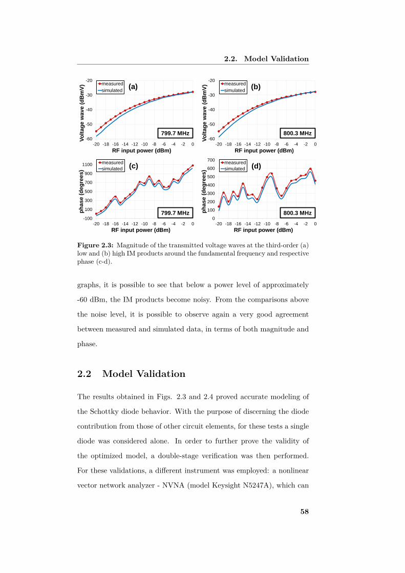
2.2. Model Validation
-60
-50
-40
-30
-20
-20 -18 -16 -14 -12 -10 -8 -6 -4 -2 0
Vo
ltag
e w
ave (
dB
mV
)
RF input power (dBm)
measured
simulated
-60
-50
-40
-30
-20
-20 -18 -16 -14 -12 -10 -8 -6 -4 -2 0
Vo
ltag
e w
ave (
dB
mV
)
RF input power (dBm)
measured
simulated
0
100
200
300
400
500
600
700
-20 -18 -16 -14 -12 -10 -8 -6 -4 -2 0
ph
as
e (
de
gre
es
)
RF input power (dBm)
measured
simulated
-100
100
300
500
700
900
1100
-20 -18 -16 -14 -12 -10 -8 -6 -4 -2 0
ph
as
e (
de
gre
es
)
RF input power (dBm)
measured
simulated
799.7 MHz 800.3 MHz
800.3 MHz799.7 MHz
(a) (b)
(c) (d)
Figure 2.3: Magnitude of the transmitted voltage waves at the third-order (a)low and (b) high IM products around the fundamental frequency and respectivephase (c-d).
graphs, it is possible to see that below a power level of approximately
-60 dBm, the IM products become noisy. From the comparisons above
the noise level, it is possible to observe again a very good agreement
between measured and simulated data, in terms of both magnitude and
phase.
2.2 Model Validation
The results obtained in Figs. 2.3 and 2.4 proved accurate modeling of
the Schottky diode behavior. With the purpose of discerning the diode
contribution from those of other circuit elements, for these tests a single
diode was considered alone. In order to further prove the validity of
the optimized model, a double-stage verification was then performed.
For these validations, a different instrument was employed: a nonlinear
vector network analyzer - NVNA (model Keysight N5247A), which can
58

2.2. Model Validation
-500
-300
-100
100
300
500
700
-20 -18 -16 -14 -12 -10 -8 -6 -4 -2 0
ph
ase
(d
eg
ree
s)
RF input power (dBm)
measured
simulated
-50
0
50
100
150
200
250
300
350
-20 -18 -16 -14 -12 -10 -8 -6 -4 -2 0
ph
ase
(d
eg
ree
s)
RF input power (dBm)
measured
simulated
-80
-70
-60
-50
-40
-30
-20 -18 -16 -14 -12 -10 -8 -6 -4 -2 0
Vo
ltag
e w
ave
(d
Bm
V)
RF input power (dBm)
measured
simulated
-60
-50
-40
-30
-20
-10
-20 -18 -16 -14 -12 -10 -8 -6 -4 -2 0
Vo
ltag
e w
ave (
dB
mV
)
RF input power (dBm)
measured
simulated
200 kHz 400 kHz
400 kHz200 kHz
(a) (b)
(c) (d)
Figure 2.4: Magnitude of the transmitted voltage waves at the (a) first and(b) second IM products in the baseband and respective phase (c-d).
be considered a mixer-based LSNA [112]. Indeed, the NVNA, also called
performance network analyzer (PNA), instead of performing a one-shot
measurement, sweeps a single local oscillator, down-converting the RF
harmonics one by one. It is possible to say that measurements with
NVNA are therefore slower, but since in this case the acquisition of the
signal is narrowband, the dynamic range of the signal is much larger
than the one of the LSNA, allowing the acquisition of signals at much
lower power levels.
2.2.1 Frequency Validation
The first verification is aimed at assessing the frequency validity of the
model, for this reason a full-wave rectifier matched at 930 MHz has been
realized, in this case employing a 0.635-mm-thick Taconic RF60A sub-
strate (εr = 6.15, tan(δ) = 0.0028 at 10 GHz). For these measurements
the NVNA source is only exploited as single-tone RF input for the rec-
59

2.2. Model Validation
Matching
network
Rectifier0
0.2
0.4
0.6
0.8
1
1.2
1.4
1.6
1.8
800 850 900 950 1000
Ou
tpu
t d
c v
olt
ag
e (
V)
Frequency (MHz)
optimized model
manufacturer model
measured
(a) (b)
Rfin = -10 dBm
Figure 2.5: (a) Picture of the full-wave rectifier and (b) and comparisonbetween measured and modeled OC dc voltage at the rectifier output, for afixed input RF power of -10 dBm.
tifier, able to provide a constant power level over frequency. The open
circuit (OC) dc voltage at the output of the rectifier is then registered
for different power levels from -20 to 0 dBm, by sweeping the RF input
frequency. Fig. 2.5(a) shows a picture of the full-wave rectifier, where
a two-stage microstrip filter is employed for matching purposes. In Fig.
2.5(b), the measurements are compared to simulations for a fixed RF
input power, where the substantial difference between the manufacturer
and the optimized model of table 2.1 is visible. A very good agreement
is observed between measured data and simulated ones employing the
optimized model. Similar behavior has been obtained for all the other
RF power levels.
2.2.2 Fundamental Frequency and Baseband Validation
In order to further verify the above-reported results, a second validation
was performed, this time investigating also the baseband response, for
another different configuration, in which the Schottky diode is used in
a single-diode rectifier with matching network at 800 MHz. In order to
assess the baseband behavior, a two-tone measurement excitation was
generated with the NVNA. In this case the frequency spacing between
the two tones was chosen equal to 10 MHz, which is the lowest frequency
60

2.2. Model Validation
(a) (b)Matching
networkRectifier
Figure 2.6: (a) Picture of the single-diode rectifier, realized on 0.76 mm-thickRogers RO3003 substrate and (b) NVNA measurement setup.
the adopted NVNA can measure at. For the verification of the BB
response, the rectifier output RC low-pass filter has been designed to
be less selective than the first intermodulation product, thus allowing
its measurement at the output of the rectifier. At the same time, the
output resistance was designed to offer the optimum loading condition
to the rectifier. In this case the two tones were excited at 800 and 810
MHz respectively, and the average power of the signal (equally divided
between the two tones) was swept over 4 values: [-16.4, -11.5, -6.6, -1.7]
dBm. A digital multimeter is connected to the “dc bias” of the NVNA
output port, in order to measure also the dc voltage at the output of the
rectifier. Fig. 2.6 shows a picture of the prototype and the measurement
setup.
During the model optimization from LSNA measurements the un-
matched condition of the previous setup was permitting only a low
amount of power to be injected inside the diode. For this reason the
model optimization led to the modification of all the optimized param-
eters reported in Table 2.1, except for the reverse breakdown voltage
(BV ). The manufacturer BV value was hence initially left unchanged,
since the model was only optimized for lower power levels, typical of
energy harvesting and wireless communication scenarios [38, 39, 118].
61
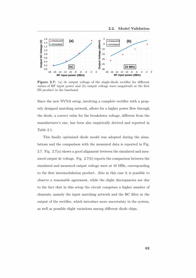
2.2. Model Validation
-30
-25
-20
-15
-10
-5
0
-18 -16 -14 -12 -10 -8 -6 -4 -2 0
Ou
tpu
t V
olt
ag
e (
dB
mV
)
RF input power (dBm)
measured
simulated
0.0
0.2
0.4
0.6
0.8
1.0
1.2
1.4
1.6
-18 -16 -14 -12 -10 -8 -6 -4 -2 0
Ou
tpu
t D
C V
olt
ag
e (
V)
RF input power (dBm)
measured
simulated
DC 10 MHz
(a) (b)
Figure 2.7: (a) dc output voltage of the single-diode rectifier for differentvalues of RF input power and (b) output voltage wave magnitude at the firstIM product in the baseband.
Since the new NVNA setup, involving a complete rectifier with a prop-
erly designed matching network, allows for a higher power flow through
the diode, a correct value for the breakdown voltage, different from the
manufacturer’s one, has been also empirically derived and reported in
Table 2.1.
This finally optimized diode model was adopted during the simu-
lations and the comparison with the measured data is reported in Fig.
2.7. Fig. 2.7(a) shows a good alignment between the simulated and mea-
sured output dc voltage. Fig. 2.7(b) reports the comparison between the
simulated and measured output voltage wave at 10 MHz, corresponding
to the first intermodulation product. Also in this case it is possible to
observe a reasonable agreement, while the slight discrepancies are due
to the fact that in this setup the circuit comprises a higher number of
elements, namely the input matching network and the RC filter at the
output of the rectifier, which introduce more uncertainty in the system,
as well as possible slight variations among different diode chips.
62

2.3. Remarks and Future Developments
2.3 Remarks and Future Developments
The demand for efficient energy management calls for new solutions
able to possibly integrate information decoding and power harvesting
in a unique operation. The reported results highlight how the available
manufacturer device model is typically not accurate enough to allow
such integrated designs. By means of a proper measurement setup, the
model of a widely adopted Schottky diode was optimized by analyzing
the baseband response to an RF two-tone excitation signal, therefore
proving the feasibility of such an integrated system for a simplified RF
multi-tone input. The same inspection was then also applied to different
rectifier configurations, as validation.
The promising results provided foster the future investigation for a
direct recovery of the information carried by a modulated signal at the
baseband output of a rectifier. Nevertheless practical implementation
of integrated data and power transfer is still facing several challenges
that call for further research efforts, encompassing different aspects of a
SWIPT system.
The research of an optimal modulated signal is of primarily impor-
tance. Indeed, the best trade-off should be chosen between the opti-
mization of the power conversion efficiency and the data transfer ca-
pability. Multi-tone signals have already proved the possibility to in-
crease the system performance in different applications. In [119, 120]
the concept of power optimized waveform (POW) has been used for im-
proving the reading range in RFIDs, while in [121] it is exploited to
enhance wake-up radios (WURs) sensitivity. Moreover, different solu-
tions have been presented to increase the RF-to-dc conversion efficiency
of a rectifier [122, 123, 124, 125, 126, 127]. In most cases high peak-to-
average power ratio (PAPR) waveform are adopted to increase rectenna
63

2.3. Remarks and Future Developments
efficiency. In particular, [126] reports closed-form equations theoreti-
cally supporting the use of PAPR waveforms, [125] provides a thorough
comparison among different approaches for the increase of rectifiers ef-
ficiency, while [127] estimates the impact of different solutions on the
choice of the rectifier optimum load. A further step is the evaluation of
the impact of different modulation schemes on the rectification capabili-
ties [128, 129, 130, 131], though a joint analysis of the operation of both
power and information transfer, as recently reported in [132], appears to
be the most reliable approach to appraise the total system performance.
64

Chapter 3
Rectenna Array for Long
Distance Autonomous IoT
Tag Localization
Next generation RFID systems are expected to provide not only secure
identification, but also advanced functionalities, one of the most urgent
being high-precision tags localization [133]. Indeed, the capability to
localize objects distributed in the environment in real-time with great
accuracy (few centimeters) would pave the way to innovative context-
aware applications with huge market potential.
Current RFID systems are usually based on the narrowband Gen. 2
standard [46], which was initially devised only for identification pur-
poses. Nevertheless, rough localization information can be obtained
exploiting different attributes of the received signal, such as: received
signal strength (RSS), signal time of arrival (TOA), time difference of ar-
rival (TDOA), or angle of arrival (AOA) [134, 135, 136, 137, 138]. These
methods can reach decimeter level accuracy in line of sight (LOS) condi-
tions, but strongly suffer from deep fading, typical of indoor multipath
65

propagation. To date, the best positioning accuracy, in the order of 3-15
cm, is offered by solutions adopting the impulse radio ultra-wideband
(UWB) technology. Indeed, when transmitting pulses with duration in
the order of a few nanoseconds, time-measurements (e.g., TOA/TDOA)
are sufficient for gathering all the necessary information from the re-
ceived signals and they are able to guarantee high localization accuracy,
thanks to the capability of easily discriminating multi-path components
[48]. Unfortunately, all available standards (e.g., IEEE 802.15.4a or
802.15.4f [139, 140]) and commercial solutions are uniquely based on
active tags (i.e. equipped with batteries and power-hungry active trans-
mitters), and hence not capable of self-sustained passive operations. In
order to guarantee high-accuracy localization along with energy auton-
omy of tags, a successful solution could be represented by the combina-
tion of UWB technology with passive backscatter modulation principles
[52], achieved by means of a proper time variation of the tag antenna
load [47].
The viability of this solution is strictly dependent on the possibility
to properly energize the passive tags with battery-less techniques. In-
deed, tag operations, such as recovery and interpretation of the received
signal and antenna load modulation, require auxiliary energy availabil-
ity. For this purpose, the combination of UWB techniques and far-field
WPT strategies at UHF frequencies is proposed, similarly to what al-
ready anticipated in Chapter 1. Nonetheless, battery-less tags make the
design of such systems very challenging, calling for extremely low power
consumption electronics and efficient energy recovery solutions.
With these premises, an indoor scenario is envisaged, where reference
nodes, referred to as UWB readers, are distributed in the environment
in fixed locations. The reference nodes are also acting as wireless UHF
66

power providers, wirelessly energizing the tags with the maximum al-
lowed RF transmitted power in the European RFID band, i.e. 2 W
ERP [75]. The system shall operate in a typical indoor harsh environ-
ment where multi-path and non line of sight (NLOS) conditions might
be frequent. Moreover, tags might be as far as 10 meters from the
reference nodes, or more. In order to satisfy the strict power budgets
dictated by the application scenario, it is essential that the intrinsic
consumption of tags be aggressively low (a few mW) and to employ elec-
tronics working at minimum operating voltages, which are in general
in the 1.8 - 3 V range. From the electronics point of view, it might
result convenient being able to satisfy the low-power requirements with-
out recurring to the development of new dedicated ICs, though at the
expense of slightly higher power consumption. Sub-mA energy harvest-
ing circuits with power conversion and management functionalities im-
plemented with discrete components have been recently designed and
successfully tested with good performance and efficiency [141], although
for piezoelectric sources. These components require at least few mW of
input dc power to work properly. For the present power management
unit (PMU) the recent, commercially available TI BQ25570 has been
adopted, well suited for ultra-low power applications [142, 143]. The
dc/dc converter is specifically designed to efficiently acquire and man-
age the mW of power generated from a variety of dc sources. In this
case the rectified voltage of the UHF rectenna is provided at its input.
This component is then responsible of increasing the dc voltage input
to higher values, usable as supply voltage of the active components of
the tag, as well as to store sufficient energy locally, to sustain a single
localization operation. During the localization phase, energy consuming
operations are executed by the tag: a microcontroller unit (MCU) is
67

3.1. System Architecture
RF energy
harvesting
UHF wakeup
radio
UWB switchSpreading
code
UHF antenna
UWB antenna
power
synch
backscatter
modulator
Figure 3.1: Schematic representation of the system architecture.
activated and a UWB switch modulates the received UWB signal for
the backscattering. Indeed, the MCU represent the most power-hungry
part of the system and strategies to keep it in an idle state for most of
the time, except during the active phases, play a crucial role [144]. To
this extent, usage of a low-power and low-latency wake-up radio (WUR)
is adopted, with the purpose of waking up the active components only
when required [145, 146].
3.1 System Architecture
The proposed system architecture is reported in Fig. 3.1 and more in
detail in Fig. 3.2, where the single electronics components are repre-
sented.
The tag is composed of a UWB antenna whose reflectivity is modu-
lated using a wideband switch loaded on short and open circuits. The
energy is provided by an energy-harvesting block working in the UHF
band, connected to a UHF antenna. As clearly seen, the dc source com-
68

3.1. System Architecture
dc/dcvoltage
monitor
data
slicerMCU switch
UWB
clock
generator
POWER MANAGEMENT
VDD
VDD
VDD
VDD
UHF
rectenna
ADDRESSING AND
BACKSCATTER SIGNAL GENERATION
VDD
RESETdc
SOURCE
C storage
power ON
switch
power ON
clock
MPPT
synch
UWB
antenna
Figure 3.2: Detailed representation of the digital electronic blocks.
ing from the rectenna has to be split into two parts: one responsible for
the provisioning of power to the tag and the other one for the WUR im-
plementation. Besides tag wake-up, the WUR is responsible also for pro-
viding the proper timing for the switch operations. As detailed in Fig.
3.2, the dc/dc boost/buck-converter regulates the voltage level to the
circuitry needs. It operates with a joint voltage monitor, which provides
the power to the circuit when it is within a given range of valid supply
voltages (between 2.3 and 2.5 V). The PMU implements also maximum
power point tracking (MPPT) in order to maximize the power extracted
from the energy harvester source. The value of the storage capacitor has
to be optimized for the best trade-off between reduced start-up times
(lower values, e.g., nF) and reduced switching of the dc/dc converter
and thus of the consumed power (higher values, e.g., µF). However, the
value of the capacitor has to be chosen large enough to sustain a single
activation of the tag and, because of the consistent overall consumption
in the active phase, this inevitably leads to long wake-up times. This
consideration further motivates the adoption of a low-latency WUR in
parallel to the main harvesting section. In the addressing segment, the
69

3.1. System Architecture
data slicer is responsible for providing a stream of digital data to the
MCU, which has to wake-up when the tag address is recognized. The
control logic then provides to the backscatter modulator the spreading
code and the proper timing for switching the RF path between open
and short circuits. The address and synchronization signals are sent by
the UHF power provider nodes, with an ON-OFF keying modulation of
the CW UHF carrier. In between each interrogation cycle, a continuous
UHF CW signal is emitted by these nodes, to let all tags collect the
sufficient energy needed to operate in case of a received interrogation.
The most stringent requirement is imposed by the PMU start-up
from a completely discharged state (cold start). In this situation the
TI BQ25570 needs an input dc voltage of 330 mV, together with a dc
input power of 15 mW. Once started, it is able to continue the charging
operation with input voltages as low as 100 mV and it consumes only 7.5
mW. These values are adopted as reference for the design of the rectifying
unit and define the maximum operative distance of the system.
3.1.1 Performance Evaluation of the Available Solution
It is worth noting that two different requirements are dictated by the
PMU, depending on whether it is in a completely discharged state or it is
already accumulating energy. When designing harvesting systems, often
the second situation is considered, therefore claiming the PMU con-
sumption in a normal operation state. This assumption, though, should
be appraised carefully. Indeed, in practical scenarios it is typically not
possible to know a priori whether the interested tag has already been ex-
posed to a favorable power delivery condition, and has therefore already
overcome the “cold start” phase, or not, and is therefore completely
inactive. For this reason, the PMU specification considered hereunder
70

3.1. System Architecture
will be all referring to the situation in which a “cold start” activation is
foreseen, which defines the most stringent requirement.
As a first evaluation, the performance of the already available so-
lution, presented in Chapter 1, are assessed. A compact, one-port,
integrated UWB-UHF tag was described, which thanks to a properly
optimized diplexer network is able to provide simultaneous UWB op-
eration and UHF energy conversion. For an evaluation of the rectenna
performance in the present scenario a UHF transmitter is considered,
emitting the maximum ERP of 2 W in the UHF band and located at
10-meter distance in free-space propagation. In the best-case RF link
conditions, i.e. with the TX antenna linearly polarized and in perfect
polarization matching with the RX dipole, given the 0 dBi gain of the
receiving antenna, the RF received power at the harvester input is -16
dBm (∼ 25.1 µW ). As described in Section 1.5.1, with this input power
level the measured dc voltage is approximately 240 mV and the RF-to-dc
conversion efficiency is equal to 29%, which results in a total available
dc power of 7.3 mW. Moreover, it is worth noting that if polarization
worsens, the available RF power is reduced and the dc output decreases
accordingly. Hence, it is clear that with a conventional rectenna design,
as the one adopted for the integrated UWB-UHF tag of Chapter 1, the
PMU requirements cannot be satisfied for the envisaged long distance
operations.
In order to obtain a higher dc voltage at the rectenna output, a
possible solution could be that of changing the rectifier topology and
implement voltage multiplication. Indeed, by increasing the number of
rectifying stages, as schematically represented in Fig. 3.3, it is possible to
obtain an according gain in terms of dc voltage. The results comparing
different multi-stage topologies are reported in Table 3.1, where one
71

3.1. System Architecture
MN
UHF
antenna RLOAD
stage #1
stage #2
stage #3
stage #N
Figure 3.3: Schematic representation of a multi-stage rectifier topology forvoltage multiplication, connected to the UHF antenna through a proper match-ing network.
Table 3.1: dc outputs of the multi-stage rectifier topology.
# stages Vdc (mV) RF-to-dc eff. Pdc (µW)
1 240 29 % 7.3
2 354 25.5 % 6.4
4 392 21 % 5.3
6 398 16 % 4.0
8 305 12 % 3.0
stage corresponds to a full-wave rectifier, identical to the one described
in Section 1.5.
The advantage obtained in terms of rectified voltage by increasing the
number of stages is evident: by merely doubling the number of stages the
330 mV voltage requirement is guaranteed. Nevertheless several draw-
backs pertain to this solution. Indeed, every additional diode employed
in the rectifier introduces also additional voltage drops, which contribute
to overall increased losses. Moreover, as the number of stages raises, the
optimum load of the rectifier assumes higher values. This twofold effect
72

3.2. Single Rectenna Design
translates in a reduction of the conversion efficiency and therefore of the
dc output power. In addition, it is also possible to observe that beyond
a certain number of stages, the increased diode losses suppress also the
advantages in terms of voltage multiplication.
3.2 Single Rectenna Design
The obtained results show that adopting a multi-stage rectifier is not a
viable solution for the present case. This outcome motivates the investi-
gation of new harvesting strategies, to increase the activation distance of
the tag. An alternative solution would be that of implementing a multi-
rectenna harvester: in this way both voltage and power multiplication
are foreseen.
In order to better address the design of a UHF rectenna array, the
integrated, one-port UWB-UHF architecture of Chapter 1 is temporar-
ily abandoned. As a first step a classical single rectenna, composed of a
UHF monopole, is first designed, to be used for performance comparison
with the correspondingly-derived array architecture. Besides the com-
parison between the single rectenna and the rectenna array, this new
single rectenna design is also employed for the analysis of a novel WUR
implementation.
As anticipated, in parallel to the rectenna design a wake-up radio is
also adopted for the present tag. The purpose of the WUR is to bound
the employment of the power-consuming components of the tag to the
sole active phase. These components can therefore be kept in an idle, lis-
tening state and be waken-up by the low-latency WUR when the specific
tag is addressed. The input for the WUR implementation has to be de-
rived from the UHF received signal. Recent designs dedicate a separate
antenna to the WUR receiver [147, 148]; this solutions, though, would
73

3.2. Single Rectenna Design
VUHF
ZANT L1
C1 C2 CUP
CDOWN
dcblock
dcblock
D1
D2
D3
D4
Vrect
CWUR
Crect
VWUR
matching net. rectifier
wake-up
cap. divider
Figure 3.4: Circuit schematic of the monopole rectenna. The RF availablepower is modeled as an ac voltage source with the antenna impedance as inter-nal resistance. Vrect and VWUR are fed at the input of the respective electronicblock described in Fig. 3.2.
require much larger tag areas, contrasting with the usual tag miniatur-
ization requirements. For this reason, the possibility to integrate the
rectification and WUR functionalities within a single antenna are much
more appealing. To this extent the most obvious solution would be that
of providing an input for the WUR by splitting the dc voltage at the out-
put of the rectifier with a conventional resistive divider. This solution,
though, is by definition lossy, as it involves lossy components. Given the
extremely low values of power available at the high distances foreseen for
the present system, loosing even only few mW of power is not acceptable.
For this reason a novel solution is proposed, where the voltage is split
at RF level, by means of a capacitive divider. In this way, only reactive
components are involved, resulting in almost no losses, except for the
parasitic ones due to the non-ideal capacitors. The capacitive divider
topology is provided in Fig. 3.4, where the rectenna circuit schematic is
shown.
Table 3.2 lists the SMD components used for the circuit, while Fig.
3.5 shows the realized rectenna prototype on a 0.5-mm-thick Rogers
74

3.2. Single Rectenna Design
Table 3.2: List of SMD components of the monopole rectenna.
Part name Manufacturer Product code Value
L1 Coilcraft 0603HP-18NXGLU 18 nH
C1 Murata GJM1555C1H120FB01 12 pF
C2 Murata GJM1555C1HR50WB01 0.5 pF
CUP Murata GJM1555C1HR70WB01 0.7 pF
CDOWN Murata GJM1555C1H1R0WB01 1 pF
dcblock ATC 600L100FT200T 10 pF
D1-D2-D3-D4 Skyworks SMS7630-079LF
Crect Murata GJM1555C1H100FB01 10 pF
CWUR Murata GJM1555C1H100FB01 10 pF
RO4350B substrate (εr = 3.48, tan(δ) = 0.0037 at 10 GHz).
Finally, the performance of the monopole rectenna are provided in
Fig. 3.6. Fig. 3.6(a) reports the values of the OC voltages at the
rectifier and wake-up outputs, for different values of available RF power
at the input of the rectenna. It is possible to see that, with the proposed
capacitive divider implementation, VWUR is a derivation of the main dc
output, corresponding to about 20-25% of Vrect. In Fig. 3.6(b) the
rectified dc voltage on the optimum load (equal to 10kΩ for the present
case), as well as the RF-to-dc conversion efficiency of the rectifier are
reported, for different RF power levels at the rectenna input. Very good
agreement between measured and simulated results is obtained in all
cases, except at the higher power levels, where the breakdown voltage
of the Schottky diode is not providing accurate model prediction, as
described in Chapter 2.
The monopole antenna exhibits a realized gain of 1.8 dBi and a
radiation efficiency of 95%. Thanks to the slightly increased radiation
75

3.2. Single Rectenna Design
105 mm
35 mm
test line
dc outputs
rectifier
+ WUR
L1
C1 C2
CUP
CDOWNdcblock
dcblockD1
D2
D4
D3
Crect
CWUR
Figure 3.5: Picture of the monopole rectenna prototype. The zoomed viewshows the layout of the rectifier and wake-up circuitry.
0
300
600
900
1200
1500
1800
2100
2400
0
10
20
30
40
50
60
-25 -20 -15 -10 -5 0
dc
Volt
age
(mV
)
Con
ver
sion
eff
icie
ncy
(%
)
Available RF input power (dB)
modeled measured
0
400
800
1200
1600
2000
2400
2800
3200
3600
-25 -20 -15 -10 -5 0
OC
Rec
tifi
ed V
olt
age
(mV
)
Available RF input power (dBm)
rect_SIM
rect_MEAS
WUR_SIM
WUR_MEAS
(a) (b)
Figure 3.6: Comparison between measured and modeled (a) OC voltages atthe output of the rectifier and wake-up sections and (b) RF-to-dc conversionefficiency and dc voltage on the optimum load of the rectifier, for differentvalues of RF input power.
76

3.2. Single Rectenna Design
performance with respect to the one provided by the antenna of Chapter
1, when transmitting 2 W ERP at 10-meter distance, the RF received
power at the harvester input is -14.3 dBm (∼ 37.2 µW ). With this
input power level the measured dc voltage is approximately 360 mV
and the RF-to-dc conversion efficiency is equal to 35%, which results in
a total available dc power of 13 mW. The obtained dc voltage is able
to satisfy the PMU requirements, although the dc power is still below
the requested value. Nevertheless, it is worth noting that also in this
case the RF received power is assessed in the best RF link conditions,
i.e. assuming perfect polarization matching between the transmitter and
the receiving antenna. The possibility to rotate the tag can be provided
by adopting a circularly polarized antenna at the transmitter side; this
however causes a 3 dB power drop, resulting in dc voltage and power
outputs of 220 mV and 5 mW, respectively. The obtained performance,
therefore, cannot be considered satisfactory.
Besides the obtained rectifier dc outputs, the designed rectenna proved
the validity of the capacitive divider solution, which is able to provide
a WUR implementation with no need for a dedicated antenna. In or-
der to assess the effectiveness of this solution, though, it is important
to evaluate how the two signals might affect each other. Indeed, since
the WUR is obtained from a direct derivation of the RF voltage which
feeds the rectifier, a variation of the loading conditions of one signal
could translate in a consequent alteration of the second one. Though
the WUR alteration due to different rectifier conditions is an obvious
consequence of the adopted capacitive divider implementation, the op-
posite case would result particularly detrimental, since the WUR should
perform its operations in a seamless fashion, without affecting the main
functionalities of the harvester.
77
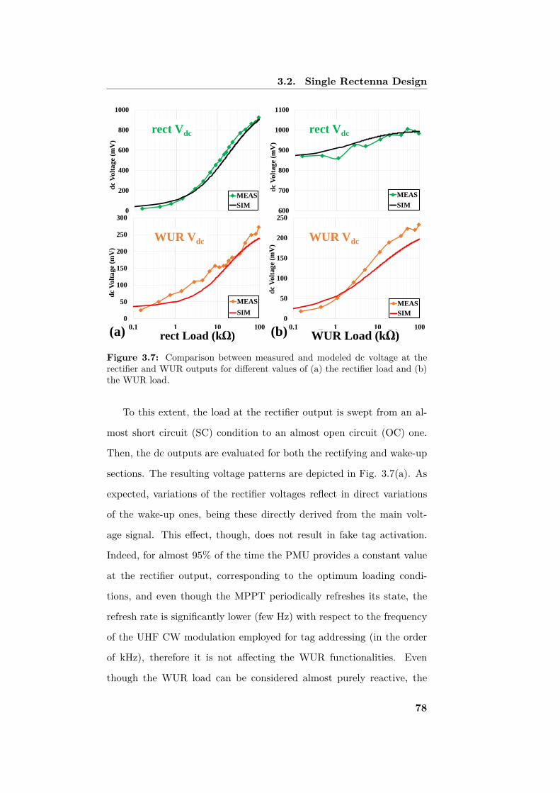
3.2. Single Rectenna Design
0
200
400
600
800
1000
0.1 1 10 100
dc
Volt
ag
e (m
V)
Rect_Load (kΩ)
MEAS
SIM600
700
800
900
1000
1100
0.1 1 10 100
dc
Volt
ag
e (m
V)
WuR_Load (kΩ)
MEAS
SIM
0
50
100
150
200
250
300
0.1 1 10 100
dc
Volt
ag
e (m
V)
rect Load (kΩ)
MEAS
SIM0
50
100
150
200
250
300
0.1 1 10 100
dc
Volt
ag
e (m
V)
rect Load (kΩ)
MEAS
SIM
0
50
100
150
200
250
0.1 1 10 100
dc
Volt
ag
e (m
V)
WUR Load (kΩ)
MEAS
SIM0
50
100
150
200
250
0.1 1 10 100
dc
Volt
ag
e (m
V)
WUR Load (kΩ)
MEAS
SIM
rect Vdc rect Vdc
WUR Vdc WUR Vdc
(a) (b)
Figure 3.7: Comparison between measured and modeled dc voltage at therectifier and WUR outputs for different values of (a) the rectifier load and (b)the WUR load.
To this extent, the load at the rectifier output is swept from an al-
most short circuit (SC) condition to an almost open circuit (OC) one.
Then, the dc outputs are evaluated for both the rectifying and wake-up
sections. The resulting voltage patterns are depicted in Fig. 3.7(a). As
expected, variations of the rectifier voltages reflect in direct variations
of the wake-up ones, being these directly derived from the main volt-
age signal. This effect, though, does not result in fake tag activation.
Indeed, for almost 95% of the time the PMU provides a constant value
at the rectifier output, corresponding to the optimum loading condi-
tions, and even though the MPPT periodically refreshes its state, the
refresh rate is significantly lower (few Hz) with respect to the frequency
of the UHF CW modulation employed for tag addressing (in the order
of kHz), therefore it is not affecting the WUR functionalities. Even
though the WUR load can be considered almost purely reactive, the
78

3.3. Four Dipoles Rectenna Array
dual evaluation is done by sweeping its value and comparing how this
translates respectively to the rectifier and the wake-up outputs. The
corresponding results are given in Fig. 3.7(b). Obviously, the voltage at
the wake-up output is changed accordingly, but it is possible to observe
that this variation exerts only a minor influence on the rectifier signal.
These evaluations are reported for a fixed available power level of -13
dBm, but equivalent conclusions are obtained all over the expected in-
cident power range. Therefore, these results prove the effectiveness of
the proposed seamless implementation of the wake-up radio.
3.3 Four Dipoles Rectenna Array
The results obtained by the reported rectenna designs are not able to
satisfy the system requirements, especially in terms of rectified power
delivered to the PMU. For this reason, the investigation of new harvest-
ing strategies is carried out, in particular focusing on the possibility to
implement a multi-rectenna harvester, for which power multiplication is
foreseen.
When it comes to rectennas connection in the design of a multi-
harvester array, two possibilities are typically envisioned: series- or
parallel-connection among the rectenna elements [149, 32, 150, 151, 152,
34, 153, 154]. In both cases an increment of the overall dc power is
expected at the array output; in case of series-connection the overall
dc voltage is also multiplied, while if a parallel-connection is adopted
the resulting dc current is augmented. The 360 mV obtained with the
monopole rectenna prototype satisfy the 330 mV requirement of the
PMU with a very short margin and only in case of perfect polariza-
tion matching with a linearly polarized transmitter. For this reason the
series-connection has been adopted in the rectenna array design, with
79

3.3. Four Dipoles Rectenna Array
the goal of satisfying the 15 mW power requisite and at the same time
guaranteeing a consistent margin in terms of dc voltage.
Regarding the choice of the array elements, a thoughtful analysis
has to be undertaken. Indeed, in most harvesting scenarios direction of
arrival and polarization of the incident RF signal is usually unknown or
time-varying. The most effective solution for unknown polarization re-
ception is the use of a couple of dual linearly-polarized antennas [95, 155]
or circularly polarized ones [156], while the unknown direction of ar-
rival forces the use of non-directional antennas, the most common being
dipole-like antennas, which have omnidirectional behavior. A dipole-like
antenna, such as the one described in Section 3.2, represents the most
adopted omnidirectional choice, but it obviously presents radiation nulls
along the dipole axis direction. A second drawback ensues from its lin-
ear polarization (LP), which can result in zero RF power at the rectenna
input in case of cross-polarized incident signals. This obstacle is often
overcome by adopting circular polarization (CP) at the transmitter side,
nevertheless in most cases a direct control on the radiofrequency source
is not possible.
For the present rectenna array a dual-linear polarization has been
adopted and further extended in order to better fulfill dc requirements:
two couples of dual linearly-polarized UHF planar dipoles are integrated
on the same substrate, together with an Archimedean spiral for UWB
communication, this way leading to a compact exploitation of the tag
area. The dual linear polarization allows to receive the same amount of
RF power irrespective of the incident polarization, i.e. CP , both left-
and right-handed, and LP, for any given polarization rotation: this rep-
resents an unreachable performance for a CP receiving antenna. More-
over, thanks to the integration of two couples of dual linearly-polarized
80

3.3. Four Dipoles Rectenna Array
-25
-20
-15
-10
-5
0
700 750 800 850 900 950 1000
Sii
(dB
)
Frequency (MHz)
|S11| |S22| |S33| |S44|
-25
-20
-15
-10
-5
0
700 750 800 850 900 950 1000
Sij
(dB
)
Frequency (MHz)
|S31| |S42| |S21| |S43|
(a) (b)
Figure 3.8: Modeled dipoles (a) reflection coefficient and (b) mutual coupling.Ports numbers are in accordance with the numbering of Fig. 3.9.
antennas, the resulting RF received power by the harvester can be fur-
ther increased, by combining the outputs of four distinct rectifiers.
Since distance among the dipoles is within fractions of wavelength,
a quite strong coupling among antenna elements is reached. Fig. 3.8(a)
reports the simulated reflection coefficients of the four dipoles. Despite
the good matching for all the elements at 868 MHz, a strong coupling is
observed in Fig. 3.8(b). The complete avoidance of this mutual influence
could be reached only by placing the antennas very far from each other,
procedure that would lead to impractical tag dimensions. For this reason
this coupling is instead exploited for the optimization of the radiation
characteristics of the tag. The integration of the five antennas on the
same device is optimized with a parametric study. The UWB spiral,
covering the 3.1 to 4.8 GHz band, is fixed in a central position. With the
goal of reaching the higher gain in all the possible directions, the dipoles
relative distance, d, with respect to the operating wavelength, has been
varied by λ/x, with x swept from 1 to 6, where x = 6 corresponds to
the minimum possible distance, i.e. dipole and spiral overlapping. Some
representative results in terms of gain patterns are reported in Fig. 3.10,
while Fig. 3.9 illustrates the optimized layout, where the UHF dipoles
have been meandered for miniaturization purpose.
81

3.3. Four Dipoles Rectenna Array
d
dipole 1
dipole 3
dipole 4 dipole 2
0.8 mm
100 mm
36 mm
x
y
z
φ
θ
Figure 3.9: Layout of the quasi-isotropic four-element harvester, co-planarwith a UWB spiral antenna for the optimum dipole distance d = λ/4.3. Di-mensions 100x100x1.5mm3, designed on Rogers RO4350B substrate (εr = 3.48,tan(δ) = 0.0037 at 10 GHz).
-3
-2
-1
0
1
2
3
Gain (dBi)
λ/2.5
λ/3.5
λ/4.5
λ/5.5
0
90
180
270
q
Figure 3.10: Gain patterns of dipole 1 in ϕ = 90°-plane (yz-plane) (see Fig.3.9), for different inter-dipole distances d = λ/x.
82

3.3. Four Dipoles Rectenna Array
Figure 3.11: 3D gain pattern of dipole 1 for the optimum dipole distanced = λ/4.3. Identical gain patterns pertain to the other three dipoles, with a 90degrees rotation along ϕ.
Fig. 3.10 displays the gain patterns of dipole 1 (see Fig. 3.9), where
the influence due to the mutual coupling with the other dipoles can be
observed. Identical gain patterns pertain to the other three dipoles, with
a 90 degrees rotation along ϕ. The distance λ/4.3, corresponding to 80
mm, has been chosen as optimal, providing the maximum gain in both
the θ = 0°, 180° (broadside) directions and the θ = 90° (lateral) direc-
tion, equal to 2.1 and 1.7 dBi, respectively. The radiation efficiency is in
this case equal to 96%. For easiness of visualization, the 3D gain pattern
of dipole 1 is also reported in Fig. 3.11. In this way the mutual coupling
among the dipoles at the optimum distance increases their directivity in
the broadside and respective lateral directions. The topological combi-
nation of the four elements leads to an overall quasi-isotropic behavior,
with no radiation nulls in any direction. This result is of paramount im-
portance in RF energy harvesting applications, as it leads to the highest
power being collected for any given orientation with respect to the RF
source.
83

3.3. Four Dipoles Rectenna Array
At this point, though, it is important to observe that, due to the
strong inter-antenna coupling, the single dipole-element impedance be-
comes useless for quantifying the true amount of RF power received
by each dipole and the actual coupling mechanism (in the near-field)
among the dipole antennas ports has to be used. Moreover, it is note-
worthy that such quantities vary with the reciprocal orientation between
the RF source and the dipoles system [157]. This can be obtained by
means of the reciprocity theorem, under the assumption of a uniform
plane wave incident on the dipoles system, with a procedure equivalent
to the one described in Section 1.5.2. In this way the Norton equiva-
lent sources of the dipoles system four-port network can be derived for
any possible combination of the RF excitation and of the dipoles system
orientation. To do so the four-port admittance matrix of the dipoles
system computed by EM simulation is used in place of the scalar one
representing each stand-alone dipole. This does have a significant im-
pact on the system description as can be seen from Fig. 3.12(a), where
the real and imaginary part of the self-admittance parameters Yii are
compared with the corresponding quantities computed for a standalone
dipole. Fig. 3.12(b) shows the trans-admittance behavior in the same
conditions. Finally, regarding the spiral antenna, its behavior is not in-
fluenced by the UHF dipoles location and it provides a maximum gain
in the broadside direction, ranging from 3 to 6 dBi over the UWB band
and with a constant radiation efficiency of 97%.
Each dipole of Fig. 3.9 is connected to a rectifying section by means
of a p-matching network. This way, four distinct rectennas are inte-
grated on the same device. In order to provide a unique dc output, a
dc-series connection is realized, therefore maximizing the overall output
voltage. A schematic of each rectifying section and of their correspond-
84

3.3. Four Dipoles Rectenna Array
-0.04
-0.02
0.00
0.02
0.04
0.06
0.75 0.8 0.85 0.9 0.95
(S)
Frequency (GHz)
Re(Y11) Re(Y33) Re(Y )
Im(Y11) Im(Y33) Im(Y )
standalone
standalone
-0.06
-0.03
0.00
0.03
0.75 0.8 0.85 0.9 0.95
(S)
Frequency (GHz)
Re(Y12) Re(Y13) Im(Y12) Im(Y13)
(a) (b)
Figure 3.12: Near-field behavior in terms of (a) self-admittances and stan-dalone dipole admittance, (b) trans-admittances.
ing connection is given in Fig. 3.13, where UHF power from each dipole
is represented as an ac voltage source with the antenna impedance as
series resistance. It is possible to observe that the capacitive divider for
the WUR output is implemented only in the first stage; indeed, for the
present system it is possible to choose the most suitable polarization
at the transmitter side and in this case a CP has been adopted for the
transmitting UHF antenna. In addition, a single WUR stage is enough,
thanks to the extremely low requirements of the WUR [121]. Never-
theless, the system could be straightforwardly adapted to the case of
unknown radiating sources by simply providing a capacitive division at
the second stage, too. In this way dual-linear polarization functionalities
can be guaranteed as well for the WUR signal.
A full-wave rectifier topology is adopted in each stage, where Schot-
tky diodes are the Skyworks SMS7630-079LF. Values of the optimized
network are given in Table 3.3, while Fig. 3.14 reports the final tag
layout on Rogers RO4350B substrate.
Validation experiments of the described tag, unfortunately, did not
provide good agreement with the predicted results. Indeed, the mea-
sured dc values obtained at the tag output were lower than expected.
85

3.3. Four Dipoles Rectenna Array
VUHF 1
ZANT 1 L1
C1A C1B CUP
CDOWN
dcblock
dcblock
Vrect
CWUR
Crect
VWUR
VUHF 2
ZANT 2 L2
C2A C2B
dcblock
Crect
VUHF 3
ZANT 3 L3
C3A C3B
dcblock
Crect
VUHF 4
ZANT 4 L4
C4A C4B
dcblock
Crect
Figure 3.13: Topology of the multi-rectenna series dc connection. Each stagenumber corresponds to the respective dipole of Fig. 3.9. Matching networks ofstages 2 to 4 are identical, while the first stage is optimized for the provisioningof the additional WUR output.
stage 4 stage 2
sta
ge 3
sta
ge
1
VWuRGNDVrect
36 mm
0.8 mm
10
0 m
m
Figure 3.14: Representation of the final layout and picture of the four-rectenna array prototype. Red lines on the left image represent metalizationson the bottom side of the PCB.
86

3.3. Four Dipoles Rectenna Array
Table 3.3: List of SMD components of the four-dipole rectenna array.
Part name Manufacturer Product code Value
L1 Coilcraft 0603HP-22NXGLW 22 nH
L2 = L3 = L4 Coilcraft 0603HP-23NXGLW 23 nH
C1A Murata GJM1555C1H150FB01D 15 pF
C1B Murata GJM1555C1HR50WB01 0.5 pF
C2A = C3A = C4A Murata GJM1555C1H9R5BB01D 9.5 pF
C2B = C3B = C4B Murata GJM1555C1H1R2WB01D 1.2 pF
CUP Murata GJM1555C1HR90WB01D 0.9 pF
CDOWN Murata GJM1555C1H1R7WB01D 1.7 pF
dcblock ATC 600L100FT200T 10 pF
diodes Skyworks SMS7630-079LF
Crect Murata GJM1555C1H390JB01D 39 pF
CWUR Murata GJM1555C1H100FB01 10 pF
87

3.3. Four Dipoles Rectenna Array
Table 3.4: OC rectified voltage comparison of the presented harvesters.
Available RF power Monopole Rectenna Four-rectenna Array
- 16 dBm 0.7 V 1.2 V
- 11 dBm 1.25 V 2.1 V
- 6 dBm 2.3 V 3.9 V
Representative results in terms of OC rectified voltage are reported in
Table 3.4, where the corresponding results of the monopole rectenna of
Section 3.2 are also reported for comparison. The available RF power
at the input of the rectenna is calculated by means of the reciprocity
theorem as previously explained. For equivalent RF power, the four-
element rectenna array is able to provide an increase of the OC voltage
of about 70% with respect to the single rectenna case. Nevertheless,
though, the corresponding optimum load value at the series-connected
rectifiers output assumes an increase value of 33 kW, therefore the re-
sulting overall dc power is slightly lower than the one provided by the
monopole rectenna. These results can be justified by the consistent
mutual coupling emerged from the tight integration among the array
elements. This coupling result in RF contributions received by each rec-
tification stage not exclusively coming from the UHF source, but also
due to the inter-exchange of power among the antennas. Since this last
phenomenon is uncontrolled, these power exchanges are able to sum to
each other with discording phases, resulting in destructive contributions.
Moreover, part of these signals can also end up being re-radiated by the
antennas, entailing an additional power loss. This outcome justifies the
imperative necessity of resorting to a more accurate design when deal-
ing with multi-rectenna array implementation, with the goal of better
controlling the resulting RF mutual influence among the array elements.
88

3.4. Two Monopoles Rectenna Array
3.4 Two Monopoles Rectenna Array
Due to the extreme close proximity of the antenna array elements, the
occurred RF coupling of the antennas ports resulted to be too strong and
a performance degradation with respect to the EM simulation-based re-
sults has been observed. The near-field elements coupling causes an un-
controlled exchange of signals (since the phases of the received waves are
uncontrolled), causing a portion of the coupled power to be re-radiated
instead of being converted to dc, as well as possible destructive signal
summations. Therefore, if not properly controlled, this mutual influence
results in significant variations of the dc rectenna outputs [158].
These results indicate that, even if the array elements are dc-connected,
a proper interface among the antennas should be designed as well at
the radiofrequency level, this way providing independent RF contribu-
tions with a suitable control over signal phases [159, 160, 161]. To this
extent, a possible solution can be represented by designing an RF de-
coupling network between the array elements [162]. This solution has
been adopted for the present tag design. In order to better control the
decoupling between the array elements a two-element array has been
adopted in this case, involving two monopole antennas. The proposed
circuit schematic of this new two monopole rectenna array is reported
in Fig. 3.15.
The antenna near-field behavior is considered by means of the 2-port
S matrix obtained by EM simulation and the UHF incident power on
each dipole is represented with an ac current source at each port in-
put. The implemented decoupling network is composed of two parallel
lumped elements and two couples of series ones, realized with SMD
components, whose values are detailed in Table 3.5. This network is
also responsible to provide proper matching conditions between the an-
89

3.4. Two Monopoles Rectenna Array
2-ports
antenna
IUHF 1
L3 C3
CUP
CDOWN
dcblock
dcblock
Vrect
CWUR
Crect
VWUR
CUP
CDOWN
dcblock
dcblock
CWUR
Crect
L2 C2
IUHF 2
L1 C1
decoupling and
matching network
test-port 2
test-port 1
Figure 3.15: Circuit schematic of the two-monopole rectenna array with de-coupling network.
tennas and the rectifying sections. In this case the WUR is implemented
at both stages, still exploiting the capacitive divider solution. It is also
possible to see that series dc connection has been realized for both the
rectifier and the WUR.
A picture of the realized prototype, realized on a 1.5-mm-thick Rogers
RO4350B substrate (εr = 3.48, tan(δ) = 0.0037 at 10 GHz), is reported
in Fig. 3.16, with the corresponding dimensions. As seen from the fig-
ure, this layout has been realized in view of a direct integration with
the electronic components on the same PCB. The inclusion of a minia-
turized UWB chip antenna is also foreseen in the space left between the
two monopoles (a proper soldering pattern is realized in this case on the
backside of the PCB).
For a proper design of the decoupling/matching circuitry, the net-
work has been first optimized by means of linear simulations, assuming a
reference value for the rectifying sections input impedance of 9− j150Ω,
90

3.4. Two Monopoles Rectenna Array
Table 3.5: List of SMD components of the two-monopole rectenna array.
Part name Manufacturer Product code Value
L1 Coilcraft 0603HP-56NXGLU 56 nH
C1 Murata GJM1555C1H2R8WB01D 2.8 pF
L2 = L3 Coilcraft 0603HP-27NXGLU 27 nH
C2 = C3 Murata GJM1555C1H390JB01D 39 pF
CUP Murata GJM1555C1HR70WB01D 0.7 pF
CDOWN Murata GJM1555C1H1R0WB01D 1 pF
dcblock ATC 600L100FT200T 10 pF
diodes Skyworks SMS7630-079LF
Crect Murata GJM1555C1H100FB01 10 pF
CWUR Murata GJM1555C1H100FB01 10 pF
105 mm
105 mm
monopole 1
monopole 2test line 1
test line 2
rect +
WUR 1
rect +
WUR 2
match.
and
decoupl.
Figure 3.16: Picture of the realized two-monopole prototype. The bottom-left part of the tag, containing a green solder mask, is designed for integrationof the electronic components.
91

3.4. Two Monopoles Rectenna Array
in correspondence of the two test ports inserted in the schematic of Fig.
3.15. Indeed, this number was found as impedance at the capacitive di-
vider input, loaded by the corresponding rectifiers, for a fixed RF power
level of -13 dBm. This value was chosen as a reference since it is the
power quantity at which PMU requirements were satisfied by the single
monopole rectenna. Obviously this is a power-dependent optimization,
which is only valid for a given RF power level of the nonlinear circuitry.
Therefore the matching conditions, and consequently the conversion ef-
ficiency, can be degraded for slightly different impedances offered by the
rectifying section at higher power levels. Nevertheless, in these condi-
tions the higher received RF power compensates the degradation of the
conversion efficiency and the dc power output is still capable of satisfying
the PMU requirements.
The modeled matching and decoupling behavior of the optimized
network are reported in Fig. 3.17 in terms of scattering parameters,
where port 1 and port 2 are the corresponding test ports of Fig. 3.15,
normalized on 9−j150Ω. The matching and decoupling conditions at the
UHF 868 MHz frequency are clearly observed. The test lines visible in
Fig. 3.16 are then exploited for the evaluation of the equivalent measured
performance. The results are superimposed in Fig. 3.17, where the S
parameters obtained with a VNA measurement at the two test ports
are reported after a proper de-embedding of the test lines [114] and a
re-normalization on 9 − j150 Ω. A quite good agreement is obtained
between simulated and measured data, despite for a small decrease in
the measured decoupling.
In order to evaluate the overall rectenna performance, the rectified
outputs are finally measured for different distances from a UHF trans-
mitter emitting the maximum value of 2 W ERP and are compared to
92

3.4. Two Monopoles Rectenna Array
-30
-25
-20
-15
-10
-5
0
550 650 750 850 950 1050
(dB
)
Frequency (GHz)
S11_mod S11_meas S21_mod S21_meas
Figure 3.17: Comparison between the measured and modeled insertion andreturn loss at the two test ports, in correspondence of the interface betweenthe decoupling network and the two rectifying sections.
the ones reached by the corresponding monopole rectenna. In this final
evaluation, a CP transmitting antenna is adopted, which introduces a
3 dB polarization mismatching. This choice however allows a less strin-
gent system operation, since tags should be able to rotate freely, without
being restricted to predefined orientation positions. The results are re-
ported in Fig. 3.18. It is possible to observe that this time the new
rectenna array provides a positive increase in terms of both voltage and
power dc outputs. The obtained rectified power is more than two times
the one provided by the single monopole rectenna, while the rectified
voltage is almost twice that reached by the single monopole. These ex-
cellent results confirm the effectiveness of the decoupling implemented
between the array elements and provide an acceptable constant satisfac-
tion of the PMU requirements for the high operation distances foreseen
by the presented system.
93
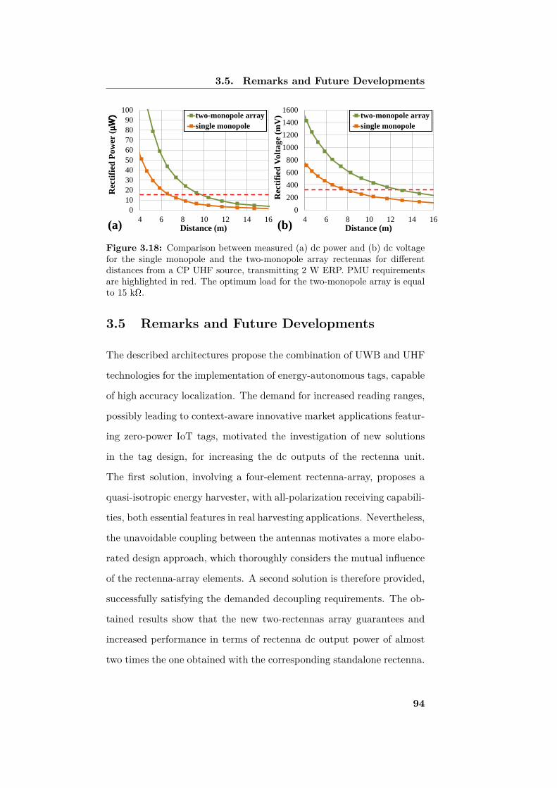
3.5. Remarks and Future Developments
0
10
20
30
40
50
60
70
80
90
100
4 6 8 10 12 14 16
Rec
tifi
ed P
ow
er (μW)
Distance (m)
two-monopole array
single monopole
0
200
400
600
800
1000
1200
1400
1600
4 6 8 10 12 14 16
Rec
tifi
ed V
olt
ag
e (m
V)
Distance (m)
two-monopole array
single monopole
(a) (b)
Figure 3.18: Comparison between measured (a) dc power and (b) dc voltagefor the single monopole and the two-monopole array rectennas for differentdistances from a CP UHF source, transmitting 2 W ERP. PMU requirementsare highlighted in red. The optimum load for the two-monopole array is equalto 15 kW.
3.5 Remarks and Future Developments
The described architectures propose the combination of UWB and UHF
technologies for the implementation of energy-autonomous tags, capable
of high accuracy localization. The demand for increased reading ranges,
possibly leading to context-aware innovative market applications featur-
ing zero-power IoT tags, motivated the investigation of new solutions
in the tag design, for increasing the dc outputs of the rectenna unit.
The first solution, involving a four-element rectenna-array, proposes a
quasi-isotropic energy harvester, with all-polarization receiving capabili-
ties, both essential features in real harvesting applications. Nevertheless,
the unavoidable coupling between the antennas motivates a more elabo-
rated design approach, which thoroughly considers the mutual influence
of the rectenna-array elements. A second solution is therefore provided,
successfully satisfying the demanded decoupling requirements. The ob-
tained results show that the new two-rectennas array guarantees and
increased performance in terms of rectenna dc output power of almost
two times the one obtained with the corresponding standalone rectenna.
94

Chapter 4
Low-Cost UHF Near-Field
Contactless Solution for
RFID Applications
Wireless power transmission in the far-field region has many potential
applications, especially for low power devices and sensors and is en-
visioned as key enabler for a pervasive deployment of the Internet of
Things. However, when dealing with consumer electronics, or more in
general with applications where power transfer efficiency and safety be-
come the main concerns, for the time being near-field WPT finds more
room for adoption, thanks to its inherent advantages. Indeed, contrary
to the far-field case, where transmission of energy is obtained through
electromagnetic propagation, in near-field WPT the exchange of energy
takes place by means of electric or magnetic coupling, with no fields be-
ing propagated outside the proximity of the WPT system [20, 163, 164].
The non-radiative exchange of energy in the near-field can be catego-
rized into three main groups, depending on the adopted type of coupling
technique: (i) inductive coupling, (ii) magnetic resonant coupling and
95

4.1. WPT for RFID Applications
(iii) capacitive coupling. The first kind of near-field coupling takes place
by induction of a magnetic field from a primary coil to a secondary coil
[16, 15, 165], which is essentially based on the same working principle of
an electrical transformer. Magnetic resonant coupling can be considered
to some extent an evolution of the inductive coupling mechanism: in
this case the primary and secondary are tuned in resonance by adding
compensation capacitors, so that the two resonators become coupled at
the same resonance frequency [166, 167, 168]. Finally, the third kind of
near-field WPT is realized by the exchange of electric field between two
adjacent capacitors [169, 170, 171], also in this case a resonant condi-
tion can be realized by implementing compensation inductors [172]. The
first two mechanism of near-field WPT are often identified as inductive
power transfer (IPT), while the last one is also referred to as capacitive
power transfer (CPT).
Each implementation has its own advantages and disadvantages, nev-
ertheless a common factor combines the majority of the well-known so-
lutions so far: in almost all cases, the operating frequency is in the range
from LF (30-300 kHz) to HF (3-30 MHz), while very few solutions have
been proposed at UHF or microwave frequencies [27, 173]. In this Chap-
ter a near-field WPT system is presented, envisioned for, but not limited
to, low-cost RFID applications in the European UHF 868 MHz band.
4.1 WPT for RFID Applications
RFID technology is a very well-know technique, which has been deeply
investigated in the last decades [174, 175, 176, 177] and since then be-
came a pervasive technology in everyday life. Its applications span a high
number of different scenarios, such as logistics and supply chain, item-
level inventory tracking, access control, mobile healthcare, distributed
96

4.1. WPT for RFID Applications
sensor networks and real time locating systems (RTLS). A key feature
demanded in the vast majority of cases is the necessity for very low-
cost materials and manufacturing techniques, both deemed important
requirements for the effective mass deployment of RFID technology in
market applications [178].
A representative example of UHF RFID application can be the cov-
erage of shelves for inventory tracking, featuring highly stacked items.
Such scenarios typically require hundreds of meters of shelves to be cov-
ered with RFID readers, compliant with the maximum EIRP emission
[75], so that every item falls within the reading range of the readers. In
order to decrease the system costs, the reader units, which represent the
expensive part of the RFID system [47], tend to be kept at the minimum
possible number. For this reason in many cases one single reader unit is
connected to different antennas by means of a multiplexer or similar kind
of splitters and the RF signal is typically propagated to the radiating
units by means of coaxial cables of different lengths. Depending on the
application scenario, the radiating units can have to be placed at a very
close distance (e.g., half a meter) and in a quite high number in order
to guarantee an acceptable coverage. Covering hundreds of meters of
shelves with such techniques results in a considerable cost, not only for
the consistent amount of required RF coaxial cables, but also in terms
of installation. Moreover, this large number of antennas should also be
able to be periodically replaced, for maintenance or upgrade needs.
In such a context, the possibility to replace physical connections
between hardware components with contactless techniques using inex-
pensive materials and featuring high repeatability is very attractive and
enabling for large-scale adoption. Fig. 4.1 depicts a schematic repre-
sentation of a possible architecture, where the signal of the main cen-
97

4.1. WPT for RFID Applications
mux
WPTAnt#1
Ant#2
Ant#3
Ant#4
RFID Reader
Unit
UHF input
Figure 4.1: Schematic representation of a contactless connection between theRFID reader processing unit and the reader antennas.
tralized reader unit is divided among different paths and is fed to sev-
eral distributed reader antennas with no need for connectors, allowing a
straightforward and easy antenna removal or replacing. Such migration
could be performed in a seamless fashion taking advantage of near-field
wireless power transmission capabilities. Nevertheless most implementa-
tions of this kind take place at the underlying low and high frequencies,
while from the RFID point of view, the simplest and less expensive
choice would be realizing near-field coupling at the same frequency of
operation of the UHF RFID communication, with no need for additional
frequency conversion modules.
Recently a method for near-field coupling at UHF has been proposed
[179, 180]. This solution exploits the resonant behavior of an optimized
defected ground structure to create a near-field coupling between two
closely spaced resonators. This method is adopted and further developed
for a low-cost implementation, envisioned for RFID applications in the
European UHF 868 MHz band.
4.1.1 DGS Resonators
Defected ground structures (DGSs) can be considered as an evolution of
photonic band gap (PBG) structures, i.e. periodic structures specifically
98

4.1. WPT for RFID Applications
PORT 2
PORT 1
TOP BOTTOM
PORT 1
PORT 2
capacitance
inductance
(a) (b)
Figure 4.2: (a) H-shaped DGS, where the capacitive and inductive areas ofthe defection are highlighted and (b) equivalent circuit representation.
designed in a way that propagation of certain frequency bands is pro-
hibited [181, 182]. As a general definition, a DGS basically consists in a
section of microstrip line which presents a removal, or defection, in the
ground plane, with a specific size and shape. Such defection introduces
a perturbation of the current distribution in the ground plane, which
results in modifications of the transmission line capacitance and induc-
tance [183]. Thanks to the quasi-lumped LC resonant circuit behavior
of the defected section, DGSs have been widely investigated in the last
years for the implementation of band-stop and band-pass planar filters
[184, 185, 186, 187, 188].
The resonance behavior of the DGS was recently proposed as a build-
ing block for wireless power transmission applications [179, 180]. Indeed,
by placing two resonant DGSs next to each other, power can be transmit-
ted wirelessly, similarly to what is done in any near-field WPT resonant
link, but with the main advantage of providing a WPT link at UHF
frequencies, exploiting the particular structure of the DGS to overcome
the usual limitation of the increased radiation resistance and losses of
inductors at higher frequencies [189].
A H-shaped DGS can be modeled as a parallel LC resonator [183,
184, 190], as schematically represented in Fig. 4.2, where the inductance
contribution mainly comes from the wider etching in the ground plane
99

4.1. WPT for RFID Applications
t = 2.55 mm
t = 50 μm
t = 10 μm
linoleum
PET
alluminum
Figure 4.3: Multilayer substrate representation. Two PET layers with printedconductive aluminum are employed as top and bottom metalization, linoleumis used as main dielectric substrate.
and the capacitive one from the center facing metalized strips. By means
of quasi-static modeling [191] it is possible to identify a relationship
among the DGS dimensions and the values of the circuit equivalent
representation [180], which can be exploited for the initial design of the
DGS.
4.1.2 Low-Cost Materials
A requirement of paramount importance in RFID systems is a low-cost
implementation. This poses strict constraints on the materials choice,
which have to be available at a very low-cost, but also on the manu-
facturing costs: adopting cheap materials that require labored and/or
expensive machining is still not acceptable in most cases. Finally, the
final products should be designed in such a way that their deployment
in the intended working environment can be achieved smoothly and eas-
ily, reducing also the deployment costs. A second feature that is of
increasing importance in many emerging applications is flexibility in the
structure, in order to be conformable with non-planar surfaces. The
choice of material should be based on these two requirements.
For this purpose thin polyethylene terephthalate (PET), which is
flexible, low-cost and widely adopted in RFID systems, especially for
100

4.2. WPT Implementation
tags realization [177, 192, 193, 194, 195], is a good candidate. Neverthe-
less, it is suitable as a supporting material for printing antennas, but it
is usually too thin to be adopted as the sole substrate for microstrip lines
and microstrip antennas. In order to provide the convenient thickness,
linoleum, a very cheap, flexible material widely used for floor covering,
though not directly suitable for RF applications, can be adopted as a
further supporting medium besides the PET. The combination of these
two materials offers a very cheap solution that can be effectively adopted
for practical applications. In order to obtain accurate modeling of the
structure, the electrical properties of the two materials are measured by
means of a standard resonant cavity method with a Damaskos Model 08
Thin Sheet Tester. The electrical properties are found to be εr = 3.2,
tan (δ) = 0.003 (at 1 GHz) and εr = 1.89, tan (δ) = 0.011 (at 1 GHz) for
PET and linoleum, respectively. By superimposing the materials, mi-
crostrip lines and antennas can be created: a schematic representation
of a possible multilayer low-cost substrate adopted for the present design
is reported in Fig. 4.3. Printed aluminum on PET is employed for the
metallic layers, while linoleum acts as main dielectric substrate. The
three layers can be simply superimposed on top of each other, without
any extra glue or fixing material.
4.2 WPT Implementation
The presented multilayer substrate is adopted for the design of H-shaped
DGSs to be used as resonators for near-field UHF WPT. As a first step
the microstrip line is truncated, acting as an open circuit stub, which
from the circuital point of view can be modeled as an additional series
capacitance. The stub length can therefore also be tuned to regulate
the resonant frequency and for matching purposes. As opposed to [180],
101

4.2. WPT Implementation
45 mm
45 mm Lstub
45 mm
45 mm LL
WLWC
0.5 mm 0.5 mm8.7 mm
(a) (b)
Figure 4.4: Schematic representation of the designed DGS: (a) top view,where the line width is set for a 50Ω characteristic impedance and (b) bottomview, showing the interdigital capacitor. The bottom dotted black line marksthe DGS section, at the far end of the multilayer microstrip line.
where the needed value of capacitance is reached by adding a lumped
SMD capacitor in parallel to the one offered by the DGS, for the present
design SMD components are avoided and an interdigital capacitor is
implemented to simplify the manufacturing and to lower the overall
costs. In this way all metallic structures are planar and can be directly
printed on a PET substrate. A 2D representation of the presented H-
shaped DGS is reported in Fig. 4.4, together with the relative parametric
dimensions.
For an effective implementation in real scenarios, the evaluation of
the impact of surrounding materials which are placed nearby the res-
onating structure has to be carried out. The strip line of the structure
reported in [180] is facing the supporting material. So, placing the whole
structure onto any material other than air will deeply affect its behavior.
Indeed, either the effective dielectric constant of the bottom microstrip
will change or it will become a stripline if it is placed on top of a metal-
lic surface. To overcome this limitation, the bottom microstrip line is
flipped over such that the ground plane is facing the supporting mate-
rial: the effect of the latter is restricted to the area of the DGS, due
to the partial metal removals in the ground plane. This way, the effect
of different materials used as support has to be evaluated only in this
102

4.2. WPT Implementation
45 mm
8.7 mm
45 mm
Lstub
port 1
port 2
DGS
section
100 mm
100 mm
microstrip 1
microstrip 2
Figure 4.5: Perspective view of the two microstrip lines ending/beginningwith the DGS section. One layer of linoleum is placed as spacer between thetwo DGSs.
region. A 3D representation of the near-field WPT system is depicted
in Fig. 4.5.
4.2.1 DGS Parametric Study
The multilayer substrate described in the previous Sections is chosen for
the investigation of the near-field coupling performance between the two
closely spaced resonators. By tuning the dimensions of the structure, a
parametric study is conducted with electromagnetic simulations, using
CST Microwave Studio [76]. As a first step, the dimensions of the in-
terdigital capacitor are found in order to provide a fixed capacitance of
approximately 1 pF [196]. Secondly, the other dimensions reported in
Fig. 4.4 are tuned in order to highlight their impact on the inductive
behavior of the DGS and therefore on the operating frequency. Fig. 4.6
illustrates some results reporting the impact of the parameters LL, WL
and WC on the resonant frequency. One parameter is changed at a time
while keeping the other two fixed. From these results, it is possible to
notice that LL has a smaller impact, it produces a shift of approximately
10-15 MHz/mm, and it is therefore suitable for fine tuning of the reso-
nant frequency. WL and WC have a greater influence, introducing shifts
of about 35-40 MHz/mm. The modification of WL is preferred since the
103

4.2. WPT Implementation
-30
-25
-20
-15
-10
-5
0
0.70 0.75 0.80 0.85 0.90 0.95
|S11
| (d
B)
Frequency (GHz)
WC=7WC=9
WL=7WL=9
LL=27LL=29
Figure 4.6: Tuning of the resonant frequency obtained by varying the signifi-cant parameters of the DGS. The black curve represents the reference startingpoint, obtained for LL = 28mm, WL = 8mm and WC = 8mm.
latter parameter influences also the interdigital capacitor. During these
tuning the length of the stubs, Lstub, is kept fixed to 20 mm.
The second significant design parameter is the distance between the
two resonators. It is well known in near-field resonant WPT applications
that by changing the distance between the two resonators a frequency
separation of the two resonances is produced [197, 198]. Even though
a possible method for obtaining constant power transfer even in case of
varying distances has been recently proposed [199], for the present appli-
cation a constant distance is foreseen throughout the whole operation of
power transfer and can therefore be chosen a priori. Such phenomenon
of frequency bifurcation is graphically described in Fig. 4.7, where the
simulated performance of the near-field coupling is reported for different
values of distance. For a real physical implementation of the structure,
the material used as spacer between the two resonators cannot simply be
free space but necessarily has to be a physical medium. Hence, to com-
ply with the low-cost requirements, the same linoleum material already
used is employed as spacer.
104

4.2. WPT Implementation
(a)
(b)
-30
-25
-20
-15
-10
-5
0
0.5 0.6 0.7 0.8 0.9 1.0 1.1 1.2
|S11| (d
B)
Frequency (GHz)
K = 1
K = 1.5
K = 2
K = 2.5
K = 3-30
-25
-20
-15
-10
-5
0
0.5 0.6 0.7 0.8 0.9 1.0 1.1 1.2
|S2
1| (d
B)
Frequency (GHz)
K = 1
K = 1.5
K = 2
K = 2.5
K = 3
-4.5
-4.0
-3.5
-3.0
-2.5
-2.0
-1.5
-1.0
0.7 0.8 0.9 1.0 1.1(b)
Figure 4.7: Effect of the varying distance between the two DGSs in termsof number of linoleum layers, K, placed as spacer between the two. One layerof linoleum has a thickness of 2.55 mm, in accordance with Fig. 4.3. DGSdimensions are in this case LL = 27 mm, WL = 8 mm, WC = 8 mm andLstub = 18mm. (a) Reflection coefficient and (b) transmission coefficient.
It is interesting to notice from the results of Fig. 4.7 that, even
though the optimum distance is given by K=3, which provides a single,
wide operating bandwidth, the maximum transmission value is obtained
for K=1, which is therefore chosen for the present design, even though
this entails a doubling of the operating bands. The 0.5-1 dB drop of
the transmission coefficient for higher values of K can be explained by
the increased quantity of lossy materials inserted between the two res-
onators. Even if it is reduced, the operating bandwidth obtained is still
well suitable for applications in the European 868 MHz band. Obviously,
in case a higher bandwidth would be required, for example for coverage
of other RFID frequency bands, the optimum distance could be chosen,
at the expense of a slight reduction of the transmission coefficient. To
this extent, a second prototype is also implemented, with K=3, in order
to test also the feasibility of the wider bandwidth solution.
105

4.2. WPT Implementation
Table 4.1: List of realized prototypes.
LL
(mm)WL
(mm)WC
(mm)Lstub
(mm)N. of layers
(K) as spacerType ofmaterial
Proto 1 26 6 7 18 1 non-metallic
Proto 2 28 9 8 14 3 non-metallic
Proto 3 27 10 11 14 1 metallic
4.2.2 Experimental Validation on Different Materials
Based on the previously described considerations, three different proto-
types of the proposed system were realized and measured. For a practical
implementation, it is extremely important to evaluate the effect of the
materials surrounding the DGS section, specifically the physical sup-
port on which the coupling structure is placed during operation. In this
Section, the effects of plastic and wood materials are first considered as
they have the same influence on the coupling structure. In a second step,
metallic material is also assessed, estimated as the most influencing yet
widely adopted medium for a vast number of applications.
Since K=1 is the distance which provides the best transmission coef-
ficient, this has been chosen for both the metallic and non-metallic cases.
In the latter, an additional prototype, with K=3, is also implemented
and measured, to assess the wider bandwidth solution. Table 4.1 sum-
marizes the three realized prototypes, together with the corresponding
dimensions.
The pictures of the two measurement setups are reported in Fig. 4.8.
In both cases, a single additional layer of linoleum is placed between the
coupling structure and the physical support.
106
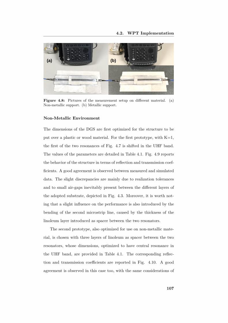
4.2. WPT Implementation
(b)(a)
Figure 4.8: Pictures of the measurement setup on different material. (a)Non-metallic support. (b) Metallic support.
Non-Metallic Environment
The dimensions of the DGS are first optimized for the structure to be
put over a plastic or wood material. For the first prototype, with K=1,
the first of the two resonances of Fig. 4.7 is shifted in the UHF band.
The values of the parameters are detailed in Table 4.1. Fig. 4.9 reports
the behavior of the structure in terms of reflection and transmission coef-
ficients. A good agreement is observed between measured and simulated
data. The slight discrepancies are mainly due to realization tolerances
and to small air-gaps inevitably present between the different layers of
the adopted substrate, depicted in Fig. 4.3. Moreover, it is worth not-
ing that a slight influence on the performance is also introduced by the
bending of the second microstrip line, caused by the thickness of the
linoleum layer introduced as spacer between the two resonators.
The second prototype, also optimized for use on non-metallic mate-
rial, is chosen with three layers of linoleum as spacer between the two
resonators, whose dimensions, optimized to have central resonance in
the UHF band, are provided in Table 4.1. The corresponding reflec-
tion and transmission coefficients are reported in Fig. 4.10. A good
agreement is observed in this case too, with the same considerations of
107

4.2. WPT Implementation
-40
-35
-30
-25
-20
-15
-10
-5
0
0.4 0.5 0.6 0.7 0.8 0.9 1.0 1.1 1.2 1.3 1.4
(dB
)
Frequency (GHz)
|S11| sim
|S11| meas
|S21| sim
|S21| meas
Figure 4.9: Comparison between simulated and measured reflection andtransmission coefficients for the first prototype, over non-metallic material.
the first prototype. Both prototypes exhibit very good performance in
terms of transmission coefficient, even though, as expected, prototype
1 reaches a maximum measured transmission coefficient of -1.3 dB, as
opposed to the -2.6 dB obtained by prototype 2, at the expenses of a
slightly reduced operating bandwidth.
Metallic Environment
In a large number of applications, the RFID operation has to take place
in close proximity of metallic objects. This represents by far the worst
possible scenario and it is therefore chosen as the second case study.
Once again, the dimensions of the structure were optimized by EM sim-
ulations.
It is found that placing the resonating structure on top of a metallic
surface exerts a significant influence on the behavior of the coupling.
In particular, the presence of the metallic surface appears to have a
detrimental effect mainly on the first of the two resonances of Fig. 4.7,
canceling it, while the second resonance is only slightly affected. This ef-
fect is explained by the fact that the first resonance is mainly attributed
108

4.2. WPT Implementation
-40
-35
-30
-25
-20
-15
-10
-5
0
0.4 0.5 0.6 0.7 0.8 0.9 1.0 1.1 1.2 1.3 1.4
(dB
)
Frequency (GHz)
|S11| sim
|S11| meas
|S21| sim
|S21| meas
Figure 4.10: Comparison between simulated and measured reflection andtransmission coefficients for the second prototype, over non-metallic material.
-40
-35
-30
-25
-20
-15
-10
-5
0
0.4 0.5 0.6 0.7 0.8 0.9 1.0 1.1 1.2 1.3 1.4
(dB
)
Frequency (GHz)
|S11| sim
|S11| meas
|S21| sim
|S21| meas
Figure 4.11: Comparison between simulated and measured reflection andtransmission coefficients for the third prototype, over metallic material.
109

4.3. RFID Reader Antenna
to the DGS closer to the metallic surface. The second resonance, con-
versely, mainly attributed to the further DGS, features only a slight
frequency shift and a small degradation in the transmission coefficient.
It is therefore chosen for the present design. A second prototype was
realized by shifting the frequency of the second resonance to be centered
at 868 MHz. The corresponding dimensions are given in Table 4.1 and
comparison between the measured and simulated data is provided in Fig.
4.11. An acceptable agreement is obtained in this case, too, even though
it is possible to observe a more adverse influence due to the presence of
nearby metallic material.
4.3 RFID Reader Antenna
As previously discussed, the present design can be applied to a large
number of applications, where the possibility of providing contactless
coupling between two planar microstrip lines that need to operate at
UHF sounds attractive. A possible implementation can be that of wire-
less connection between an RFID reader unit and its antenna. Indeed,
there are a several number of cases in which the radiating element of an
RFID reader needs to be replaced or modified in a certain way. Since
these kinds of operations typically involve a very high number of units at
a time, a contactless connection can result in a significant cost reduction
with respect to a solution requiring physical connections. Moreover, its
high repeatability can easily speed up the entire process.
4.3.1 Antenna Implementation
As a proof of concept, a UHF microstrip patch antenna is designed and
realized on the same multilayer substrate of Fig. 4.3, it is then connected
to the microstrip line corresponding to the second DGS of Fig. 4.5, in
110

4.3. RFID Reader Antenna
UHF IN(port 1)
DGS section
microstrip 1
patch
antenna
microstrip 2
34 mm
122 mm
14
5 m
m
Figure 4.12: Schematic representation of a possible application for RFIDantenna contactless feeding.
correspondence of the port 2 termination. The designed patch antenna
is fed with an inset of 34 mm for impedance matching and it has a
width and length of 145 and 122 mm, respectively. The dimensions of
the DGS are the same as those employed for prototype 1, with K=1,
except for the stubs which are in this case tuned to different lengths for
matching purposes, since the loads of the two DGSs are different in the
present case. In particular, the length of the stub fed by port 1 is fixed
to 16 mm, while the length of the second stub, connected to the patch
antenna, is chosen equal to 20 mm. A schematic representation of the
patch antenna contactless feeding is reported in Fig. 4.12.
In the first place, the feasibility of the contactless antenna feeding
is tested in terms of return loss at port 1. A comparison between the
measured and modeled data is provided in Fig. 4.13. First, it is possible
to notice the suppression of the second resonance, previously seen in
Figs. 4.7-4.9, due to the loading of the second termination with the patch
antenna, whose impedance is obviously frequency dependent. Second, it
is possible to observe an excellent matching for the antenna, nevertheless
exhibiting the usual frequency shift due to air-gaps.
The resonance is moved from the designed 868 MHz up to 915 MHz.
Such shift finds theoretical justification by manually inserting in the EM
111

4.3. RFID Reader Antenna
-25
-20
-15
-10
-5
0
0.4 0.5 0.6 0.7 0.8 0.9 1.0 1.1 1.2 1.3 1.4
(dB
)
Frequency (GHz)
|S11| sim
|S11| meas
-25
-20
-15
-10
-5
0
0.75 0.80 0.85 0.90 0.95 1.00
(dB
)
Frequency (GHz)
Figure 4.13: Comparison between the measured and simulated contactlessfed patch antenna return loss. In the zoomed graph it is possible to observethe frequency shift due to air-gaps.
simulations a constant air-gap of about 130µm among the layers of Fig.
4.3, value that can be reasonably expected, since the several layers are
simply superimposed on top of each other.
From EM simulation, the system is expected to provide a maximum
realized gain equal to 4.9 dBi and a radiation efficiency of 45%, values
mainly limited by the employed lossy substrate.
In order to verify this performance, the contactless fed patch antenna
is finally tested inside an anechoic chamber. A picture of the DUT is
shown in Fig. 4.14. Given the frequency shift, observed in Fig. 4.13, the
measurements in the anechoic chamber are performed in correspondence
of the shifted resonance at 915 MHz. The measured gain patterns in both
H- and E-plane are depicted in Fig. 4.15, superimposed to the modeled
ones.
These measurements validate once again the excellent performance
of the contactless fed antenna, with a measured maximum realized gain
of 3.7 MHz.
112

4.3. RFID Reader Antenna
Figure 4.14: Picture of the realized contactless fed patch antenna prototype,tested in the anechoic chamber.
-35-30-25-20-15-10
-505
measured-CO
measured-CROSS
modelled-CO
modelled-CROSS
Rea
lize
d G
ain
(d
Bi)
0
90
180
270
θ°
-35-30-25-20-15-10
-505
measured-CO
measured-CROSS
modelled-CO
modelled-CROSS
Rea
lize
d G
ain
(d
Bi)
0
90
180
270
θ°
H plane E plane
Figure 4.15: Measured and simulated gain patterns of the contactless fedmicrostrip patch antenna, in both H- and E-planes.
113

4.4. Remarks and Future Developments
4.4 Remarks and Future Developments
The presented systems demonstrates a novel low-cost implementation
for contactless near-field coupling between two resonating structure at
UHF for European 868 MHz RFID applications. The effects of different
nearby low-cost materials used as support for the resonant structure are
evaluated and the EM design is confirmed by measurement results. The
substrate and the power transfer technique used in the present study
entitle the proposed system for wide deployment in mass market ap-
plications thanks to the very low cost and high repeatability. For fu-
ture possible realization the possibility to print aluminum directly on
linoleum (or similar materials) should be investigated, for example by
means of the well-known techniques of inkjet printing [84, 200]. This
would lead to the twofold advantage of increasing speed in the manufac-
turing and elimination of the air-gaps.
114
Conclusions
This doctoral thesis describes the main outcomes of the research ac-
tivity conducted throughout the duration of the Ph.D. program. Some
innovative solutions for wireless power transmission and radiofrequency
energy harvesting were successfully achieved and have here been re-
ported.
The system detailed in Chapter 1 illustrates the implementation of
a novel, single-port, compact, low-profile tag, capable of hybrid UWB-
UHF operations, with the goal of providing sensing, communication and
high accuracy localization/tracking functions [50]. The miniaturized,
eco-compatible architecture has dimensions suitable for current and fu-
ture RFID applications. UWB technology, for accurate localization and
communication, and a UHF rectenna, for efficient RF energy harvest-
ing, can be exploited simultaneously thanks to the excellent performance
provided by the diplexer network, both in terms of respective matching
and strong decoupling between the two operating bands. The designed
diplexer miniaturization exerts only minor influence on antenna perfor-
mance and provides a final tag thickness lower than 1 mm. It is notewor-
thy that such influence can be totally overcome by future UWB-UHF
integrated chip, to be directly connected in the inner part of the antenna
115
Conclusions
port. Numerical EM simulations have been validated by measurements,
performed in real application scenarios, therefore proving the readiness
of the tag for direct adoption in future RFID networks. The implemen-
tation on paper substrate guarantees eco-compatibility for more than
93% of the total tag volume, enabling the proposed solution for per-
vasive, massive market applications. Despite the non-negligible losses
of the substrate, the antenna performances are fully compatible with
UWB communication and UHF energy harvesting requirements. Nev-
ertheless, exploitation of alternative recyclable materials, introducing
lower losses (e.g., PET, fabrics), can be straightforwardly addressed by
simply scaling the antenna layout. Consequently, the high performance,
simultaneous data and power transfer capabilities, compact low-profile
structure and eco-compatible material, recommend the proposed tag for
next-generation UWB-based RFID systems.
The activity described in Chapter 3 can be considered a natural evo-
lution of the first one. Where the combination of UWB and UHF tech-
nologies is still exploited for the implementation of energy-autonomous
tags, featuring accurate localization. The demand for increased reading
ranges motivated the investigation of new solutions in the tag design, for
increasing the dc outputs of the rectenna unit. The first solution, involv-
ing a four-element rectenna-array, showcased a quasi-isotropic energy
harvester, with all-polarization receiving capabilities, both essential fea-
tures in real harvesting applications. Nevertheless, a consistent coupling
between the antenna elements was observed, whose proper consideration
is of paramount importance in rectenna-array design. A second solution
is therefore provided, successfully satisfying decoupling requirements.
The new two-rectennas array guarantees and increased performance in
terms of rectenna dc output power of almost two times the one obtained
116

Conclusions
with the standalone rectenna.
Finally, Chapter 4 illustrates a new near-field wireless power trans-
fer implementation, on planar low-cost substrate. Thanks to its high
repeatability and very-low-cost deployment, the proposed system can
be a possible candidate for mass market RFID applications.
117

Acknowledgements
Desidero innanzitutto ringraziare i miei relatori, Prof.ssa Alessandra
Costanzo e Prof. Diego Masotti, per il loro supporto e per la loro guida
in questo percorso di crescita degli ultimi anni.
Ringrazio la mia fidanzata (e a breve sposa) Jessica, per essermi
sempre stata vicino. Mia madre Mariarosa, mio padre Lauro e mia
sorella Alessandra, il cui sostegno non è mai mancato. Mia nonna Tilde
e tutta la mia famiglia.
Ringrazio inoltre i compagni di avventure del laboratorio, i momenti
difficili non sono mancati, ma il successo è stato superarli insieme.
Penso che non scorderò mai questa esperienza. Il cammino di questi
anni mi ha permesso di crescere enormemente, sia dal punto di vista pro-
fessionale che personale. Mi ha permesso di viaggiare, di apprezzare con-
dizioni e situazioni culturali lontane dalla nostra, di vivere in prima per-
sona nuove realtà. Opportunità spesso sottovalutate, ma che mi rendo
conto non dovrebbero essere private a nessuno degli innumerevoli tal-
enti italiani. Sperando che la consapevolezza del valore del Dottorato di
Ricerca acquisti sempre più lo spazio che merita, ringrazio tutti quelli
che hanno reso quest’esperienza possibile e così unica.
Grazie a tutti!
118

List of Achievements
Publications
Journals
1. M. Fantuzzi, D. Masotti, and A. Costanzo, “A Novel Integrated
UWB-UHF One-Port Antenna for Localization and Energy Har-
vesting,” IEEE Trans. Antennas Propag., vol. 63, no. 9, pp.
3839-3848, Sept 2015.
2. V. Palazzi, M. D. Prete, and M. Fantuzzi, “Scavenging for Energy:
A Rectenna Design for Wireless Energy Harvesting in UHF Mobile
Telephony Bands,” IEEE Microw. Mag., vol. 18, no. 1, pp. 91-99,
Jan 2017.
3. A. Costanzo, D. Masotti, M. Fantuzzi, and M. D. Prete, “Co-
Design Strategies for Energy-Efficient UWB and UHF Wireless
Systems,” IEEE Trans. Microw. Theory Techn., vol. 65, no. 5,
pp. 1852-1863, May 2017.
4. A. Costanzo, D. Dardari, J. Aleksandravicius, N. Decarli, M. Del
Prete, D. Fabbri, M. Fantuzzi, A. Guerra, D. Masotti, M. Pizzotti,
and A. Romani, “Energy Autonomous UWB Localization,” IEEE
J. Radio Freq. Identification, vol. 1, no. 3, pp. 228-244, Sept.
2017.
119

List of Achievements
Conference Papers
5. A. Costanzo, D. Masotti, P. Francia, and M. Fantuzzi, “Detection
and movement estimation of items by a smart microwave hand-
held reader,” in 2014 IEEE RFID Technology and Applications
Conference (RFID-TA), pp. 214-218, Sept 2014.
6. A. Costanzo, M. Fantuzzi, D. Masotti, and V. Rizzoli, “A Mi-
crowave Displacement Sensor System Exploiting Electromagnetic
Interferometry,” in XX Riunione Nazionale di Elettromagnetismo
(RiNEm), pp. 345-348, Sept 2014.
7. D. Masotti, A. Costanzo, M. Fantuzzi, F. Mastri, M. Aldrigo, and
M. Dragoman, “Graphene-based nano-rectenna in the far infrared
frequency band,” in 2014 44th European Microwave Conference
(EuMC), pp. 1202-1205, Oct 2014.
8. M. Fantuzzi, D. Masotti, and A. Costanzo, “Simultaneous UHF
energy harvesting and UWB-RFID communication,” in 2015 IEEE
MTT-S International Microwave Symposium (IMS), pp. 1-4, May
2015.
9. A. Costanzo, M. Fantuzzi, D. Masotti, F. Mastri, and V. Rizzoli,
“A rigorous circuit-level description of IR-UWB links,” in 2015
International Conference on Electromagnetics in Advanced Appli-
cations (ICEAA), pp. 553-556, Sept 2015.
10. M. Fantuzzi, D. Masotti, and A. Costanzo, “A multilayer compact-
size UWB-UHF antenna system for novel RFID applications,” in
2015 European Microwave Conference (EuMC), pp. 255-258, Sept
2015.
11. M. Fantuzzi, D. Masotti, and A. Costanzo, “Electromagnetic pre-
120

List of Achievements
diction of antenna layout impact on UWB localization and sens-
ing,” in 2015 International EURASIP Workshop on RFID Tech-
nology (EURFID), pp. 16-21, Oct 2015.
12. N. Decarli, A. Guerra, F. Guidi, M. Chiani, D. Dardari, A. Costanzo,
M. Fantuzzi, D. Masotti, S. Bartoletti, J. S. Dehkordi, A. Conti,
A. Romani, M. Tartagni, R. Alesii, P. D. Marco, F. Santucci, L.
Roselli, M. Virili, P. Savazzi, and M. Bozzi, “The GRETA ar-
chitecture for energy ecient radio identication and localization,”
in 2015 International EURASIP Workshop on RFID Technology
(EURFID), pp. 1-8, Oct 2015.
13. M. Fantuzzi, M. Rajabi, G. Avolio, A. Costanzo, and D. Schreurs,
“Large signal rectier characterization for simultaneous data and
Power Transfer,” in 2016 IEEE Wireless Power Transfer Confer-
ence (WPTC), pp. 1-4, May 2016.
14. D. Masotti, M. Fantuzzi, and A. Costanzo, “Next generation zero-
power RFID-tag for UWB pervasive identication,” in 2016 IEEE
International Smart Cities Conference (ISC2), pp. 1-4, Sept 2016.
15. M. Fantuzzi, D. Masotti, and A. Costanzo, “UWB-UHF RFID Tag
on Paper for Simultaneous Communication and RF Energy Har-
vesting,” in XXI Riunione Nazionale di Elettromagnetismo (RiNEm),
pp. 1-4, Sept 2016.
16. M. Fantuzzi, M. D. Prete, D. Masotti, and A. Costanzo, “Quasi-
isotropic RF energy harvester for autonomous long distance IoT
operations,” in 2017 IEEE MTT-S International Microwave Sym-
posium (IMS), pp. 1345-1348, June 2017.
17. A. Costanzo, D. Masotti, M. Fantuzzi, F. Berra, and M. D. Prete,
121

List of Achievements
“Solutions for simultaneous wireless information and power trans-
fer,” in 2017 International Conference on Electromagnetics in Ad-
vanced Applications (ICEAA), pp. 1898-1901, Sept 2017.
18. M. Fantuzzi, A. Costanzo, S. Tedjini, and P. Lemaitre-Auger,
“Low-Cost UHF Near-Field Power Transmission for RFID Appli-
cations,” in 2017 European Microwave Conference (EuMC), pp.
212-215, Oct 2017.
Invited Talks
• A. Costanzo, D. Masotti, and M. Fantuzzi, “RF-baseband nonlin-
ear co-design of zero-power harvesting systems”, Workshop “Non-
linear RFID systems, characterization and exploitation”, in IEEE
MTT-S International Microwave Symposium (IMS), 17-22 May
2015.
• A. Costanzo, D. Masotti, and M. Fantuzzi, “Combining UWB-
and UHF-RFID for Localization and Sensing”, Workshop “Euro-
pean Initiatives to Develop Wireless Power Supply for Sensor Node
Evolution”, in IEEE Radio and Wireless Week (RWW), 24-27 Jan.
2016.
Awards and Recognitions
• Winner (team) of ESoA-COST IC1301 Student Design Competi-
tion “Wireless Networks: from Energy Harvesting to Information
Processing” – Barcelona (Spain), Nov. 2015.
• Winner of IEEE MTT-S 2016 Graduate Fellowship Award, May
2016.
122

List of Achievements
• Winner (team) of 2016 International Microwave Symposium (IMS)
Student Design Competition “Wireless Energy Harvesting” – San
Francisco (USA), May 2016.
• Winner of COST IC1301 Student Paper Competition – Aalborg
(Denmark), Sep. 2016.
• Third place at University of Bologna 3MT® (Three Minutes The-
sis) Competition – Bologna (Italy), Mar. 2017.
• Finalist at 2017 International Microwave Symposium (IMS) 3MT®
(Three Minutes Thesis) Competition – Hawai’i (USA), Jun. 2017.
• Winner of SIEm-GTTI Student Paper Competition – Udine (Italy),
Jun. 2017.
123

Bibliography
[1] W. C. Brown, “The History of Power Transmission by Radio
Waves,” IEEE Trans. Microw. Theory Techn., vol. 32, pp. 1230–
1242, Sep 1984.
[2] B. Strassner and K. Chang, “Microwave Power Transmission: His-
torical Milestones and System Components,” Proc. IEEE, vol. 101,
pp. 1379–1396, June 2013.
[3] N. Tesla, "The true wireless," Electrical Experimenter, May 1919.
[4] N. Tesla, “Apparatus for transmitting electrical energy,” Dec 1914.
US Patent 4 119 732.
[5] G. Falciasecca and B. Valotti, “Guglielmo Marconi: The pioneer
of wireless communications,” in 2009 European Microwave Con-
ference (EuMC), pp. 544–546, Sept 2009.
[6] H. Matsumoto, “Research on solar power satellites and microwave
power transmission in Japan,” IEEE Microw. Mag., vol. 3, pp. 36–
45, Dec 2002.
[7] J. O. McSpadden and J. C. Mankins, “Space solar power programs
and microwave wireless power transmission technology,” IEEE Mi-
crow. Mag., vol. 3, pp. 46–57, Dec 2002.
124

Bibliography
[8] P. Jaffe and J. McSpadden, “Energy Conversion and Transmission
Modules for Space Solar Power,” Proc. IEEE, vol. 101, pp. 1424–
1437, June 2013.
[9] S. Sasaki, K. Tanaka, and K. i. Maki, “Microwave Power Transmis-
sion Technologies for Solar Power Satellites,” Proc. IEEE, vol. 101,
pp. 1438–1447, June 2013.
[10] W. C. Brown and E. E. Eves, “Beamed microwave power transmis-
sion and its application to space,” IEEE Trans. Microw. Theory
Techn., vol. 40, pp. 1239–1250, Jun 1992.
[11] N. B. Carvalho, A. Georgiadis, A. Costanzo, H. Rogier, A. Collado,
J. A. García, S. Lucyszyn, P. Mezzanotte, J. Kracek, D. Masotti,
A. J. S. Boaventura, M. de las Nieves Ruíz Lavín, M. Piñuela, D. C.
Yates, P. D. Mitcheson, M. Mazanek, and V. Pankrac, “Wireless
Power Transmission: R amp;D Activities Within Europe,” IEEE
Trans. Microw. Theory Techn., vol. 62, pp. 1031–1045, April 2014.
[12] Wireless Power Consortium. Online: http://www.wirelesspower-
consortium.com/.
[13] AirFuel (merger of Alliance for Wireless Power and Power Matter
Alliance). Online: http://www.airfuel.org/.
[14] A. W. Green and J. T. Boys, “10 kHz inductively coupled power
transfer-concept and control,” in 1994 Fifth International Confer-
ence on Power Electronics and Variable-Speed Drives, pp. 694–699,
Oct 1994.
[15] S. Y. R. Hui and W. W. C. Ho, “A new generation of universal con-
tactless Battery Charging platform for portable Consumer Elec-
125

Bibliography
tronic equipment,” IEEE Trans. Power Electron., vol. 20, pp. 620–
627, May 2005.
[16] C.-S. Wang, O. H. Stielau, and G. A. Covic, “Design considerations
for a contactless electric vehicle battery charger,” IEEE Trans.
Ind. Electron., vol. 52, pp. 1308–1314, Oct 2005.
[17] G. A. Covic and J. T. Boys, “Inductive Power Transfer,” Proc.
IEEE, vol. 101, pp. 1276–1289, June 2013.
[18] I. Mayordomo, T. Dräger, P. Spies, J. Bernhard, and A. Pflaum,
“An Overview of Technical Challenges and Advances of Inductive
Wireless Power Transmission,” Proc. IEEE, vol. 101, pp. 1302–
1311, June 2013.
[19] A. P. Sample, B. H. Waters, S. T. Wisdom, and J. R. Smith,
“Enabling Seamless Wireless Power Delivery in Dynamic Envi-
ronments,” Proc. IEEE, vol. 101, pp. 1343–1358, June 2013.
[20] J. Garnica, R. A. Chinga, and J. Lin, “Wireless Power Trans-
mission: From Far Field to Near Field,” Proc. IEEE, vol. 101,
pp. 1321–1331, June 2013.
[21] Powermat. Online: https://www.powermat.com/.
[22] Wipower. Online: https://www.qualcomm.com/prod-
ucts/wipower.
[23] WiTricity. Online: http://witricity.com/.
[24] U. K. Madawala and D. J. Thrimawithana, “A Bidirectional In-
ductive Power Interface for Electric Vehicles in V2G Systems,”
IEEE Trans. Ind. Electron., vol. 58, pp. 4789–4796, Oct 2011.
126

Bibliography
[25] G. A. Covic and J. T. Boys, “Modern Trends in Inductive Power
Transfer for Transportation Applications,” IEEE Trans. Emerg.
Sel. Topics Power Electron., vol. 1, pp. 28–41, March 2013.
[26] J. Shin, S. Shin, Y. Kim, S. Ahn, S. Lee, G. Jung, S. J. Jeon,
and D. H. Cho, “Design and Implementation of Shaped Magnetic-
Resonance-Based Wireless Power Transfer System for Roadway-
Powered Moving Electric Vehicles,” IEEE Trans. Ind. Electron.,
vol. 61, pp. 1179–1192, March 2014.
[27] S. Kim, J. S. Ho, and A. S. Y. Poon, “Wireless Power Transfer
to Miniature Implants: Transmitter Optimization,” IEEE Trans.
Antennas Propag., vol. 60, pp. 4838–4845, Oct 2012.
[28] J. S. Ho, S. Kim, and A. S. Y. Poon, “Midfield Wireless Powering
for Implantable Systems,” Proc. IEEE, vol. 101, pp. 1369–1378,
June 2013.
[29] A. Kurs, A. Karalis, R. Moffatt, J. D. Joannopoulos, P. Fisher, and
M. Soljačić, “Wireless Power Transfer via Strongly Coupled Mag-
netic Resonances,” Science, vol. 317, no. 5834, pp. 83–86, 2007.
[30] W. C. Brown, “An experimental low power density rectenna,” in
1991 IEEE MTT-S International Microwave Symposium Digest,
pp. 197–200 vol.1, July 1991.
[31] N. Shinohara and H. Matsumoto, “Experimental study of large
rectenna array for microwave energy transmission,” IEEE Trans.
Microw. Theory Techn., vol. 46, pp. 261–268, Mar 1998.
[32] L. W. Epp, A. R. Khan, H. K. Smith, and R. P. Smith, “A compact
dual-polarized 8.51-GHz rectenna for high-voltage (50 V) actua-
127

Bibliography
tor applications,” IEEE Trans. Microw. Theory Techn., vol. 48,
pp. 111–120, Jan 2000.
[33] N. Shinohara, “Beam Control Technologies With a High-Efficiency
Phased Array for Microwave Power Transmission in Japan,” Proc.
IEEE, vol. 101, pp. 1448–1463, June 2013.
[34] A. Massa, G. Oliveri, F. Viani, and P. Rocca, “Array Designs for
Long-Distance Wireless Power Transmission: State-of-the-Art and
Innovative Solutions,” Proc. IEEE, vol. 101, pp. 1464–1481, June
2013.
[35] J. A. Hagerty, F. B. Helmbrecht, W. H. McCalpin, R. Zane, and
Z. B. Popovic, “Recycling ambient microwave energy with broad-
band rectenna arrays,” IEEE Trans. Microw. Theory Techn.,
vol. 52, pp. 1014–1024, March 2004.
[36] E. Falkenstein, M. Roberg, and Z. Popovic, “Low-Power Wireless
Power Delivery,” IEEE Trans. Microw. Theory Techn., vol. 60,
pp. 2277–2286, July 2012.
[37] H. J. Visser and R. J. M. Vullers, “RF Energy Harvesting and
Transport for Wireless Sensor Network Applications: Principles
and Requirements,” Proc. IEEE, vol. 101, pp. 1410–1423, June
2013.
[38] M. Piñuela, P. D. Mitcheson, and S. Lucyszyn, “Ambient RF En-
ergy Harvesting in Urban and Semi-Urban Environments,” IEEE
Trans. Microw. Theory Techn., vol. 61, pp. 2715–2726, July 2013.
[39] S. Kim, R. Vyas, J. Bito, K. Niotaki, A. Collado, A. Georgiadis,
and M. M. Tentzeris, “Ambient RF Energy-Harvesting Technolo-
128

Bibliography
gies for Self-Sustainable Standalone Wireless Sensor Platforms,”
Proc. IEEE, vol. 102, pp. 1649–1666, Nov 2014.
[40] IHS Technology - IoT platforms: enabling the Internet of Things.
March 2016. Online: https://cdn.ihs.com/www/pdf/enabling-
IOT.pdf.
[41] Open Geospatial Consortium, "OGC Abstract Specification". On-
line: http://www.opengeospatial.org/docs/as.
[42] M. Botts, G. Percivall, C. Reed, and J. Davidson, OGC Sensor
Web Enablement: Overview and High Level Architecture, pp. 175–
190. Berlin, Heidelberg: Springer Berlin Heidelberg, 2008.
[43] Kevin Ashton, "That ’Internet of Things’ Thing", RFID Journal.
Online: http://www.rfidjournal.com/articles/view?4986.
[44] M. Belleville, H. Fanet, P. Fiorini, P. Nicole, M. Pelgrom,
C. Piguet, R. Hahn, C. V. Hoof, R. Vullers, M. Tartagni, and
E. Cantatore, “Energy autonomous sensor systems: Towards a
ubiquitous sensor technology,” Microelectronics Journal, vol. 41,
no. 11, pp. 740–745, 2010. IEEE International Workshop on Ad-
vances in Sensors and Interfaces 2009.
[45] Z. Popovic, E. A. Falkenstein, D. Costinett, and R. Zane, “Low-
Power Far-Field Wireless Powering for Wireless Sensors,” Proc.
IEEE, vol. 101, pp. 1397–1409, June 2013.
[46] EPCTM Radio-Frequency Identity Protocols Generation-2 UHF
RFID, v 2.0.1, 2015.
[47] K. Finkenzeller, RFID Handbook: Fundamentals and Applications
in Contactless Smart Cards and Identification. Wiley, 2 ed., 2003.
129

Bibliography
[48] D. Dardari, M. Luise, and E. Falletti, Satellite and terrestrial radio
positioning techniques: a signal processing perspective. Elsevier,
1 ed., 2011.
[49] R. Verdone, D. Dardari, G. Mazzini, and A. Conti, Wireless Sen-
sor and Actuator Networks - Technologies, Analysis and Design.
Elsevier, 1 ed., 2008.
[50] Italian National project PRIN-GRETA ("GREen TAgs and sensors
with ultra-wideband identification and localization capabilities"),
2012-2015. Online: http://www.greentags.eu/.
[51] M. Chiani and A. Giorgetti, “Coexistence Between UWB and
Narrow-Band Wireless Communication Systems,” Proc. IEEE,
vol. 97, pp. 231–254, Feb 2009.
[52] D. Dardari, R. D’Errico, C. Roblin, A. Sibille, and M. Z. Win, “Ul-
trawide Bandwidth RFID: The Next Generation?,” Proc. IEEE,
vol. 98, pp. 1570–1582, Sept 2010.
[53] C. Xu and C. L. Law, “TOA Estimator for UWB Backscattering
RFID System with Clutter Suppression Capability,” EURASIP J.
Wireless Comm. Net., vol. 2010, p. 753129, Jun 2010.
[54] N. Decarli, F. Guidi, and D. Dardari, “A Novel Joint RFID and
Radar Sensor Network for Passive Localization: Design and Per-
formance Bounds,” IEEE J. Sel. Topics Signal Process., vol. 8,
pp. 80–95, Feb 2014.
[55] A. Ramos, D. Girbau, A. Lázaro, A. Collado, and A. Geor-
giadis, “Solar-Powered Wireless Temperature Sensor Based on
UWB RFID With Self-Calibration,” IEEE Sensors J., vol. 15,
pp. 3764–3772, July 2015.
130

Bibliography
[56] V. Lakafosis, A. Rida, R. Vyas, L. Yang, S. Nikolaou, and M. M.
Tentzeris, “Progress Towards the First Wireless Sensor Networks
Consisting of Inkjet-Printed, Paper-Based RFID-Enabled Sensor
Tags,” Proc. IEEE, vol. 98, pp. 1601–1609, Sept 2010.
[57] ETSI EN 302 065, "Electromagnetic compatibility and Radio spec-
trum Matters (ERM); Short Range Devices (SRD) using Ultra
Wide Band technology (UWB) for communications purposes", v
1.2.1, 2010.
[58] D. Masotti, A. Costanzo, P. Francia, M. Filippi, and A. Ro-
mani, “A Load-Modulated Rectifier for RF Micropower Harvesting
With Start-Up Strategies,” IEEE Trans. Microw. Theory Techn.,
vol. 62, pp. 994–1004, April 2014.
[59] R. D’Errico, M. Bottazzi, F. Natali, E. Savioli, S. Bartoletti,
A. Conti, D. Dardari, N. Decarli, F. Guidi, F. Dehmas, L. Ou-
vry, U. Alvarado, N. Hadaschik, C. Franke, Z. Mhanna, M. Sacko,
Y. Wei, and A. Sibille, “An UWB-UHF semi-passive RFID System
for localization and tracking applications,” in 2012 IEEE Interna-
tional Conference on RFID-Technologies and Applications (RFID-
TA), pp. 18–23, Nov 2012.
[60] C. C. Cruz, J. R. Costa, and C. A. Fernandes, “Hybrid UHF/UWB
Antenna for Passive Indoor Identification and Localization Sys-
tems,” IEEE Trans. Antennas Propag., vol. 61, pp. 354–361, Jan
2013.
[61] A. Ramos, A. Lazaro, and D. Girbau, “Semi-Passive Time-Domain
UWB RFID System,” IEEE Trans. Microw. Theory Techn.,
vol. 61, pp. 1700–1708, April 2013.
131

Bibliography
[62] M. Pigeon, R. D’Errico, and C. Delaveaud, “UHF-UWB tag an-
tenna for passive RFID applications,” in 2013 7th European Con-
ference on Antennas and Propagation (EuCAP), pp. 3968–3972,
April 2013.
[63] V. Rizzoli, A. Costanzo, and P. Spadoni, “Computer-Aided Design
of Ultra-Wideband Active Antennas by Means of a New Figure of
Merit,” IEEE Microw. Compon. Lett., vol. 18, pp. 290–292, April
2008.
[64] Y. Lu, Y. Huang, Y. C. Shen, and H. T. Chattha, “A further
study of planar UWB monopole antennas,” in 2009 Loughborough
Antennas Propagation Conference, pp. 353–356, Nov 2009.
[65] W. Wiesbeck, G. Adamiuk, and C. Sturm, “Basic Properties
and Design Principles of UWB Antennas,” Proc. IEEE, vol. 97,
pp. 372–385, Feb 2009.
[66] E. Gazit, “Improved design of the Vivaldi antenna,” IEE Proc-H,
vol. 135, pp. 89–92, April 1988.
[67] W. L. Stutzman and G. A. Thiele, Antenna Theory and Design.
Wiley, 3 ed., 2013.
[68] O. A. Mashaal, S. K. A. Rahim, A. Y. Abdulrahman, M. I.
Sabran, M. S. A. Rani, and P. S. Hall, “A Coplanar Waveguide
Fed Two Arm Archimedean Spiral Slot Antenna With Improved
Bandwidth,” IEEE Trans. Antennas Propag., vol. 61, pp. 939–943,
Feb 2013.
[69] A. R. Guraliuc, R. Caso, P. Nepa, and J. L. Volakis, “Numeri-
cal Analysis of a Wideband Thick Archimedean Spiral Antenna,”
IEEE Antennas Wireless Propag. Lett., vol. 11, pp. 168–171, 2012.
132

Bibliography
[70] M. Lee, B. A. Kramer, C.-C. Chen, and J. L. Volakis, “Broadband
Spiral Antenna Miniaturization Limit,” in 2006 IEEE Antennas
and Propagation Society International Symposium, pp. 3701–3704,
July 2006.
[71] B. A. Kramer, C. C. Chen, M. Lee, and J. L. Volakis, “Fun-
damental Limits and Design Guidelines for Miniaturizing Ultra-
Wideband Antennas,” IEEE Antennas Propag. Mag., vol. 51,
pp. 57–69, Aug 2009.
[72] B. A. Kramer, M. Lee, C.-C. Chen, and J. L. Volakis, “Design
and performance of an ultrawide-band ceramic-loaded slot spiral,”
IEEE Trans. Antennas Propag., vol. 53, pp. 2193–2199, July 2005.
[73] M. Aldrigo, A. Costanzo, D. Masotti, C. Baldisserri, I. Dumitru,
and C. Galassi, “Numerical and experimental characterization of
a button-shaped miniaturized UHF antenna on magneto-dielectric
substrate,” Int. J. Microw. Wireless Tech., vol. 5, no. 3, pp. 231–
239, 2013.
[74] C. Ding, C. Ruan, L. Peng, and J. Chu, “A novel archimedean
spiral antenna with uniplanar EBG substrate,” in 2008 8th Inter-
national Symposium on Antennas, Propagation and EM Theory,
pp. 313–315, Nov 2008.
[75] ETSI EN 302 208-1, "Radio Frequency Identification Equipment
operating in the band 865 MHz to 868 MHz with power levels up
to 2 W", v 2.1.0, 2014.
[76] Computer Simulation Technologies (CST) Studio Suite. Online:
http://www.cst.com.
133

Bibliography
[77] K. D. Palmer and M. W. van Rooyen, “Simple broadband measure-
ments of balanced loads using a network analyzer,” IEEE Trans.
Instrum. Meas., vol. 55, pp. 266–272, Feb 2006.
[78] K. Hirose, M. Miyamoto, and H. Nakano, “A two-wire spiral an-
tenna with unbalanced feed,” in IEEE Antennas and Propaga-
tion Society International Symposium. 2001 Digest. Held in con-
junction with: USNC/URSI National Radio Science Meeting (Cat.
No.01CH37229), vol. 4, pp. 128–131 vol.4, July 2001.
[79] R. K. Tallos, Z. Wang, and J. L. Volakis, “Wi-Fi energy harvest-
ing system using body-worn antennas,” in 2014 IEEE Antennas
and Propagation Society International Symposium (APSURSI),
pp. 1405–1406, July 2014.
[80] Skyworks Solutions Inc., Surface Mount Mixer and Detector Schot-
tky Diodes - SMS7630-079LF, 2016.
[81] D. Masotti, A. Costanzo, F. Mastri, M. Aldrigo, and V. Rizzoli,
“Nonlinear/electromagnetic co-design of MIMO and UWB radio
links,” in Computational Electromagnetics International Workshop
(CEM), 2011, pp. 47–52, Aug 2011.
[82] E. A. Navarro, J. M. Blanes, J. A. Carrasco, and C. Reig, “Yagi-
Like Printed Antennas for Wireless Sensor Networks,” in 2007
International Conference on Sensor Technologies and Applications
(SENSORCOMM 2007), pp. 254–259, Oct 2007.
[83] M. D. Prete, D. Masotti, N. Arbizzani, and A. Costanzo,
“Remotely Identify and Detect by a Compact Reader With
Mono-Pulse Scanning Capabilities,” IEEE Trans. Microw. The-
ory Techn., vol. 61, pp. 641–650, Jan 2013.
134

Bibliography
[84] L. Yang, A. Rida, R. Vyas, and M. M. Tentzeris, “RFID Tag and
RF Structures on a Paper Substrate Using Inkjet-Printing Tech-
nology,” IEEE Trans. Microw. Theory Techn., vol. 55, pp. 2894–
2901, Dec 2007.
[85] S. Kim, A. Georgiadis, A. Collado, and M. M. Tentzeris, “An
Inkjet-Printed Solar-Powered Wireless Beacon on Paper for Iden-
tification and Wireless Power Transmission Applications,” IEEE
Trans. Microw. Theory Techn., vol. 60, pp. 4178–4186, Dec 2012.
[86] B. S. Cook and A. Shamim, “Inkjet Printing of Novel Wideband
and High Gain Antennas on Low-Cost Paper Substrate,” IEEE
Trans. Antennas Propag., vol. 60, pp. 4148–4156, Sept 2012.
[87] S. Kim, C. Mariotti, F. Alimenti, P. Mezzanotte, A. Georgiadis,
A. Collado, L. Roselli, and M. M. Tentzeris, “No Battery Re-
quired: Perpetual RFID-Enabled Wireless Sensors for Cognitive
Intelligence Applications,” IEEE Microw. Mag., vol. 14, pp. 66–77,
July 2013.
[88] Y. Kawahara, S. Hodges, N. W. Gong, S. Olberding, and
J. Steimle, “Building Functional Prototypes Using Conductive
Inkjet Printing,” IEEE Pervasive Comput., vol. 13, pp. 30–38,
July 2014.
[89] C. Mariotti, F. Alimenti, P. Mezzanotte, M. Dionigi, M. Virili,
S. Giacomucci, and L. Roselli, “Modeling and characterization of
copper tape microstrips on paper substrate and application to 24
GHz branch-line couplers,” in 2013 European Microwave Confer-
ence, pp. 794–797, Oct 2013.
135

Bibliography
[90] A. Costanzo, M. Dionigi, D. Masotti, M. Mongiardo, G. Monti,
L. Tarricone, and R. Sorrentino, “Electromagnetic Energy Har-
vesting and Wireless Power Transmission: A Unified Approach,”
Proc. IEEE, vol. 102, pp. 1692–1711, Nov 2014.
[91] H. J. Visser, S. Keyrouz, and A. B. Smolders, “Optimized rectenna
design,” Wireless Power Transfer, vol. 2, no. 1, pp. 44–50, 2015.
[92] N. Decarli, A. Guerra, F. Guidi, M. Chiani, D. Dardari,
A. Costanzo, M. Fantuzzi, D. Masotti, S. Bartoletti, J. S. Dehko-
rdi, A. Conti, A. Romani, M. Tartagni, R. Alesii, P. D. Marco,
F. Santucci, L. Roselli, M. Virili, P. Savazzi, and M. Bozzi, “The
GRETA architecture for energy efficient radio identification and
localization,” in 2015 International EURASIP Workshop on RFID
Technology (EURFID), pp. 1–8, Oct 2015.
[93] D. Dardari, A. Conti, U. Ferner, A. Giorgetti, and M. Z. Win,
“Ranging With Ultrawide Bandwidth Signals in Multipath Envi-
ronments,” Proc. IEEE, vol. 97, pp. 404–426, Feb 2009.
[94] V. Rizzoli, F. Mastri, A. Costanzo, and D. Masotti, “Harmonic-
Balance Algorithms for the Circuit-Level Nonlinear Analysis of
UWB Receivers in the Presence of Interfering Signals,” IEEE
Trans. Comput.-Aided Design Integr. Circuits Syst., vol. 28,
pp. 516–527, April 2009.
[95] A. Georgiadis, G. V. Andia, and A. Collado, “Rectenna design and
optimization using reciprocity theory and harmonic balance anal-
ysis for electromagnetic (EM) energy harvesting,” IEEE Antennas
Wireless Propag. Lett., vol. 9, pp. 444–446, 2010.
136

Bibliography
[96] A. Costanzo, A. Romani, D. Masotti, N. Arbizzani, and V. Riz-
zoli, “RF/baseband co-design of switching receivers for multiband
microwave energy harvesting,” Sensors and Actuators A: Physical,
vol. 179, pp. 158–168, Mar 2012.
[97] A. Costanzo, F. Mastri, D. Masotti, and V. Rizzoli, “Circuit-
level nonlinear/EM co-simulation and co-design of UWB re-
ceivers,” in 2011 IEEE International Conference on Ultra-
Wideband (ICUWB), pp. 425–429, Sept 2011.
[98] F. Guidi, N. Decarli, S. Bartoletti, A. Conti, and D. Dardari, “De-
tection of Multiple Tags Based on Impulsive Backscattered Sig-
nals,” IEEE Trans. Commun., vol. 62, pp. 3918–3930, Nov 2014.
[99] E. Hossain, M. Rasti, H. Tabassum, and A. Abdelnasser, “Evolu-
tion toward 5G multi-tier cellular wireless networks: An interfer-
ence management perspective,” IEEE Wireless Commun., vol. 21,
pp. 118–127, June 2014.
[100] J. Huang, C. C. Xing, and C. Wang, “Simultaneous Wireless In-
formation and Power Transfer: Technologies, Applications, and
Research Challenges,” IEEE Commun. Mag., vol. 55, pp. 26–32,
Nov 2017.
[101] X. Zhou, R. Zhang, and C. K. Ho, “Wireless Information and
Power Transfer: Architecture Design and Rate-Energy Tradeoff,”
IEEE Trans. Commun., vol. 61, pp. 4754–4767, November 2013.
[102] I. Krikidis, S. Timotheou, S. Nikolaou, G. Zheng, D. W. K. Ng, and
R. Schober, “Simultaneous wireless information and power trans-
fer in modern communication systems,” IEEE Commun. Mag.,
vol. 52, pp. 104–110, Nov 2014.
137

Bibliography
[103] Z. Ding, C. Zhong, D. W. K. Ng, M. Peng, H. A. Suraweera,
R. Schober, and H. V. Poor, “Application of smart antenna tech-
nologies in simultaneous wireless information and power transfer,”
IEEE Commun. Mag., vol. 53, pp. 86–93, April 2015.
[104] T. W. Yoo and K. Chang, “Theoretical and experimental develop-
ment of 10 and 35 GHz rectennas,” IEEE Trans. Microw. Theory
Techn., vol. 40, pp. 1259–1266, Jun 1992.
[105] J. O. McSpadden, L. Fan, and K. Chang, “Design and experiments
of a high-conversion-efficiency 5.8-GHz rectenna,” IEEE Trans.
Microw. Theory Techn., vol. 46, pp. 2053–2060, Dec 1998.
[106] J. C. Pedro and N. B. Carvalho, Intermodulation Distortion in
Microwave and Wireless Circuits. 685 Canton Street Norwood,
02062, MA, USA: Artech House, Inc., 2003.
[107] J. H. Kim, J. Bito, and M. M. Tentzeris, “Design optimization
of an energy harvesting RF-DC conversion circuit operating at
2.45GHz,” in 2015 IEEE International Symposium on Antennas
and Propagation USNC/URSI National Radio Science Meeting,
pp. 1280–1281, July 2015.
[108] I. Ramos and Z. Popovic, “A compact 2.45 GHz, low power
wireless energy harvester with a reflector-backed folded dipole
rectenna,” in 2015 IEEE Wireless Power Transfer Conference
(WPTC), pp. 1–3, May 2015.
[109] M. Fantuzzi, D. Masotti, and A. Costanzo, “A multilayer compact-
size UWB-UHF antenna system for novel RFID applications,” in
2015 European Microwave Conference (EuMC), pp. 255–258, Sept
2015.
138

Bibliography
[110] C. H. P. Lorenz, S. Hemour, and K. Wu, “Physical Mechanism and
Theoretical Foundation of Ambient RF Power Harvesting Using
Zero-Bias Diodes,” IEEE Trans. Microw. Theory Techn., vol. 64,
pp. 2146–2158, July 2016.
[111] G. Pailloncy, G. Avolio, M. Myslinski, Y. Rolain, M. V. Bossche,
and D. Schreurs, “Large-Signal Network Analysis Including the
Baseband,” IEEE Microw. Mag., vol. 12, pp. 77–86, April 2011.
[112] W. V. Moer and L. Gomme, “NVNA versus LSNA: enemies or
friends?,” IEEE Microw. Mag., vol. 11, pp. 97–103, Feb 2010.
[113] E. H. Fooks and R. A. Zakarevičius, Microwave Engineering Using
Microstrip Circuits. Upper Saddle River, NJ, USA: Prentice-Hall,
Inc., 1990.
[114] G. Crupi and D. M.-P. Schreurs, Microwave De-embedding - From
Theory to Applications. Elsevier, 1 ed., 2013.
[115] Keysight Advanced Design System (ADS). Online:
http://www.keysight.com/en/pc-1297113/advanced-design-
system-ads?nid=-34346.0&cc=US&lc=eng.
[116] G. Massobrio and P. Antognetti, Semiconductor Device Modeling
with SPICE. McGraw-Hill, 2 ed., 1993.
[117] T. J. Lee, P. Patil, C. Y. Hu, M. Rajabi, S. Farsi, and D. M.
M. P. Schreurs, “Design of efficient rectifier for low-power wireless
energy harvesting at 2.45 GHz,” in 2015 IEEE Radio and Wireless
Symposium (RWS), pp. 47–49, Jan 2015.
[118] X. Lu, P. Wang, D. Niyato, D. I. Kim, and Z. Han, “Wireless
Networks With RF Energy Harvesting: A Contemporary Survey,”
139

Bibliography
IEEE Communications Surveys Tutorials, vol. 17, pp. 757–789,
Secondquarter 2015.
[119] M. S. Trotter, J. D. Griffin, and G. D. Durgin, “Power-optimized
waveforms for improving the range and reliability of RFID sys-
tems,” in 2009 IEEE International Conference on RFID, pp. 80–
87, April 2009.
[120] A. J. S. Boaventura and N. Carvalho, “Extending Reading Range
of Commercial RFID Readers,” IEEE Trans. Microw. Theory
Techn., vol. 61, pp. 633–640, Jan 2013.
[121] M. D. Prete, A. Costanzo, M. Magno, D. Masotti, and L. Benini,
“Optimum Excitations for a Dual-Band Microwatt Wake-Up Ra-
dio,” IEEE Trans. Microw. Theory Techn., vol. 64, pp. 4731–4739,
Dec 2016.
[122] A. S. Boaventura and N. B. Carvalho, “Maximizing DC power
in energy harvesting circuits using multisine excitation,” in 2011
IEEE MTT-S International Microwave Symposium, pp. 1–4, June
2011.
[123] C. L. Yang, C. L. Tsai, Y. L. Yang, and C. S. Lee, “Enhance-
ment of Wireless Power Transmission by Using Novel Multitone
Approaches for Wireless Recharging,” IEEE Antennas Wireless
Propag. Lett., vol. 10, pp. 1353–1357, 2011.
[124] A. Collado and A. Georgiadis, “Improving wireless power trans-
mission efficiency using chaotic waveforms,” in 2012 IEEE/MTT-S
International Microwave Symposium Digest, pp. 1–3, June 2012.
[125] A. Boaventura, D. Belo, R. Fernandes, A. Collado, A. Georgiadis,
and N. B. Carvalho, “Boosting the Efficiency: Unconventional
140

Bibliography
Waveform Design for Efficient Wireless Power Transfer,” IEEE
Microw. Mag., vol. 16, pp. 87–96, April 2015.
[126] C. R. Valenta, M. M. Morys, and G. D. Durgin, “Theoretical
Energy-Conversion Efficiency for Energy-Harvesting Circuits Un-
der Power-Optimized Waveform Excitation,” IEEE Trans. Mi-
crow. Theory Techn., vol. 63, pp. 1758–1767, May 2015.
[127] F. Bolos, J. Blanco, A. Collado, and A. Georgiadis, “RF Energy
Harvesting From Multi-Tone and Digitally Modulated Signals,”
IEEE Trans. Microw. Theory Techn., vol. 64, pp. 1918–1927, June
2016.
[128] H. Sakaki, K. Nishikawa, S. Yoshida, and S. Kawasaki, “Modu-
lated scheme and input power impact on rectifier RF-DC efficiency
for WiCoPT system,” in 2015 European Microwave Conference
(EuMC), pp. 60–63, Sept 2015.
[129] H. Shimamura, R. Tanaka, H. Sakaki, S. Yoshida, K. Nishikawa,
and S. Kawasaki, “Impact of symbol rate and roll-off factor on
rectifier RF-DC conversion efficiency for WiCoPT system,” in 2016
46th European Microwave Conference (EuMC), pp. 934–937, Oct
2016.
[130] M. Rajabi, S. Pollin, and D. Schreurs, “Hybrid rectifier-receiver
node,” in 2017 IEEE MTT-S International Microwave Symposium
(IMS), pp. 1038–1041, June 2017.
[131] N. Pan, D. Belo, M. Rajabi, D. Schreurs, N. B. Carvalho, and
S. Pollin, “Bandwidth Analysis of RF-DC Converters Under Mul-
tisine Excitation,” IEEE Trans. Microw. Theory Techn., vol. 66,
pp. 791–802, Feb 2018.
141

Bibliography
[132] S. Claessens, M. Rajabi, N. Pan, S. Pollin, and D. Schreurs,
“Measurement-based analysis of the throughput-power level trade-
off with modulated multisine signals in a SWIPT system,” in 2017
89th ARFTG Microwave Measurement Conference (ARFTG),
pp. 1–4, June 2017.
[133] D. Zhang, L. T. Yang, M. Chen, S. Zhao, M. Guo, and Y. Zhang,
“Real-Time Locating Systems Using Active RFID for Internet of
Things,” IEEE Syst. J., vol. 10, pp. 1226–1235, Sept 2016.
[134] R. Miesen, R. Ebelt, F. Kirsch, T. Schäfer, G. Li, H. Wang, and
M. Vossiek, “Where is the Tag?,” IEEE Microw. Mag., vol. 12,
pp. S49–S63, Dec 2011.
[135] R. Miesen, F. Kirsch, and M. Vossiek, “Holographic localization
of passive UHF RFID transponders,” in 2011 IEEE International
Conference on RFID, pp. 32–37, April 2011.
[136] Y. Ma, L. Zhou, K. Liu, and J. Wang, “Iterative Phase Reconstruc-
tion and Weighted Localization Algorithm for Indoor RFID-Based
Localization in NLOS Environment,” IEEE Sensors J., vol. 14,
pp. 597–611, Feb 2014.
[137] L. Qiu, Z. Huang, N. Wirström, and T. Voigt, “3DinSAR: Ob-
ject 3D localization for indoor RFID applications,” in 2016 IEEE
International Conference on RFID (RFID), pp. 1–8, May 2016.
[138] A. Costanzo, D. Masotti, T. Ussmueller, and R. Weigel, “Tag,
You’re It: Ranging and Finding via RFID Technology,” IEEE Mi-
crow. Mag., vol. 14, pp. 36–46, July 2013.
[139] IEEE Std 802.15.4a-2007, pp. 1-203, Aug 2007.
[140] IEEE Std 802.15.4f-2012, pp. 1-72, Apr 2012.
142

Bibliography
[141] A. Romani, M. Filippi, M. Dini, and M. Tartagni, “A Sub-µA
Stand-By Current Synchronous Electric Charge Extractor for
Piezoelectric Energy Harvesting,” AMC J. Emerg. Technol. Com-
put. Syst., vol. 12, Jul 2015.
[142] Texas Instruments Inc., BQ25570 Nano Power Boost Charger and
Buck Converter for Energy Harvester Powered Applications, 2015.
[143] H. W. Pflug, H. J. Visser, and S. Keyrouz, “Practical applications
of radiative wireless power transfer,” in 2015 IEEE Wireless Power
Transfer Conference (WPTC), pp. 1–4, May 2015.
[144] E. Popovici, M. Magno, and S. Marinkovic, “Power management
techniques for Wireless Sensor Networks: A review,” in 5th IEEE
International Workshop on Advances in Sensors and Interfaces
IWASI, pp. 194–198, June 2013.
[145] M. Magno and L. Benini, “An ultra low power high sensitivity
wake-up radio receiver with addressing capability,” in 2014 IEEE
10th International Conference on Wireless and Mobile Computing,
Networking and Communications (WiMob), pp. 92–99, Oct 2014.
[146] M. D. Prete, D. Masotti, A. Costanzo, M. Magno, and L. Benini,
“A dual-band wake-up radio for ultra-low power Wireless Sensor
Networks,” in 2016 IEEE Topical Conference on Wireless Sensors
and Sensor Networks (WiSNet), pp. 81–84, Jan 2016.
[147] M. Magno, N. Jackson, A. Mathewson, L. Benini, and E. Popovici,
“Combination of hybrid energy harvesters with MEMS piezoelec-
tric and nano-Watt radio wake up to extend lifetime of system
for wireless sensor nodes,” in 26th International Conference on
Architecture of Computing Systems 2013, pp. 1–6, Feb 2013.
143

Bibliography
[148] R. Piyare, A. L. Murphy, C. Kiraly, P. Tosato, and D. Brunelli,
“Ultra Low Power Wake-Up Radios: A Hardware and Network-
ing Survey,” IEEE Communications Surveys Tutorials, vol. 19,
pp. 2117–2157, Fourthquarter 2017.
[149] N. Shinohara and H. Matsumoto, “Dependence of dc output of
a rectenna array on the method of interconnection of its array
elements,” Electrical Engineering in Japan, vol. 125, no. 1, pp. 9–
17, 1998.
[150] B. Strassner and K. Chang, “5.8-GHz circularly polarized recti-
fying antenna for wireless microwave power transmission,” IEEE
Trans. Microw. Theory Techn., vol. 50, pp. 1870–1876, Aug 2002.
[151] Y.-J. Ren and K. Chang, “New 5.8-GHz circularly polarized
retrodirective rectenna arrays for wireless power transmission,”
IEEE Trans. Microw. Theory Techn., vol. 54, pp. 2970–2976, July
2006.
[152] U. Olgun, C. C. Chen, and J. L. Volakis, “Investigation of
Rectenna Array Configurations for Enhanced RF Power Harvest-
ing,” IEEE Antennas Wireless Propag. Lett., vol. 10, pp. 262–265,
2011.
[153] R. Yuwono, M. A. Hamdany, F. K. Dwi, N. Auliya, and Aisah,
“Serial rectifier antenna to increase its output power,” in 2016 In-
ternational Seminar on Intelligent Technology and Its Applications
(ISITIA), pp. 451–456, July 2016.
[154] D. J. Lee, S. J. Lee, I. J. Hwang, W. S. Lee, and J. W. Yu, “Hy-
brid Power Combining Rectenna Array for Wide Incident Angle
144

Bibliography
Coverage in RF Energy Transfer,” IEEE Trans. Microw. Theory
Techn., vol. 65, pp. 3409–3418, Sept 2017.
[155] H. Sun and W. Geyi, “A New Rectenna With All-Polarization-
Receiving Capability for Wireless Power Transmission,” IEEE An-
tennas Wireless Propag. Lett., vol. 15, pp. 814–817, 2016.
[156] A. Costanzo, F. Donzelli, D. Masotti, and V. Rizzoli, “Rigorous
design of RF multi-resonator power harvesters,” in Proceedings of
the Fourth European Conference on Antennas and Propagation,
pp. 1–4, April 2010.
[157] V. Rizzoli, A. Costanzo, and G. Monti, “General electromag-
netic compatibility analysis for nonlinear microwave integrated
circuits,” in 2004 IEEE MTT-S International Microwave Sym-
posium Digest (IEEE Cat. No.04CH37535), vol. 2, pp. 953–956
Vol.2, June 2004.
[158] H. Kamoda, M. Hanazawa, S. Kitazawa, H. Ban, and
K. Kobayashi, “Mutual coupling effect on rectenna array for
RF energy harvesting,” in 2013 European Microwave Conference,
pp. 503–506, Oct 2013.
[159] A. Stjernman, “Relationship between radiation pattern correlation
and scattering matrix of lossless and lossy antennas,” Electronics
Letters, vol. 41, pp. 678–680, June 2005.
[160] C. Craeye and D. González-Ovejero, “A review on array mutual
coupling analysis,” Radio Science, vol. 46, no. 2, 2011.
[161] M. S. Sharawi, “Printed Multi-Band MIMO Antenna Systems
and Their Performance Metrics,” IEEE Antennas Propag. Mag.,
vol. 55, pp. 218–232, Oct 2013.
145

Bibliography
[162] S. C. Chen, Y. S. Wang, and S. J. Chung, “A Decoupling Tech-
nique for Increasing the Port Isolation Between Two Strongly Cou-
pled Antennas,” IEEE Trans. Antennas Propag., vol. 56, pp. 3650–
3658, Dec 2008.
[163] L. Xie, Y. Shi, Y. T. Hou, and A. Lou, “Wireless power transfer
and applications to sensor networks,” IEEE Wireless Commun.,
vol. 20, pp. 140–145, August 2013.
[164] A. M. Jawad, R. Nordin, S. K. Gharghan, H. M. Jawad, and
M. Ismail, “Opportunities and Challenges for Near-Field Wireless
Power Transfer: A Review,” Energies, vol. 10, no. 7, 2017.
[165] W. X. Zhong, X. Liu, and S. Y. R. Hui, “A Novel Single-
Layer Winding Array and Receiver Coil Structure for Contactless
Battery Charging Systems With Free-Positioning and Localized
Charging Features,” IEEE Trans. Ind. Electron., vol. 58, pp. 4136–
4144, Sept 2011.
[166] B. L. Cannon, J. F. Hoburg, D. D. Stancil, and S. C. Goldstein,
“Magnetic Resonant Coupling As a Potential Means for Wireless
Power Transfer to Multiple Small Receivers,” IEEE Trans. Power
Electron., vol. 24, pp. 1819–1825, July 2009.
[167] T. Imura and Y. Hori, “Maximizing Air Gap and Efficiency of
Magnetic Resonant Coupling for Wireless Power Transfer Using
Equivalent Circuit and Neumann Formula,” IEEE Trans. Ind.
Electron., vol. 58, pp. 4746–4752, Oct 2011.
[168] H. Kim, C. Song, D. H. Kim, D. H. Jung, I. M. Kim, Y. I. Kim,
J. Kim, S. Ahn, and J. Kim, “Coil Design and Measurements
of Automotive Magnetic Resonant Wireless Charging System for
146

Bibliography
High-Efficiency and Low Magnetic Field Leakage,” IEEE Trans.
Microw. Theory Techn., vol. 64, pp. 383–400, Feb 2016.
[169] M. P. Theodoridis, “Effective Capacitive Power Transfer,” IEEE
Trans. Power Electron., vol. 27, pp. 4906–4913, Dec 2012.
[170] H. Funato, H. Kobayashi, and T. Kitabayashi, “Analysis of trans-
fer power of capacitive power transfer system,” in 2013 IEEE 10th
International Conference on Power Electronics and Drive Systems
(PEDS), pp. 1015–1020, April 2013.
[171] J. Dai and D. C. Ludois, “Single Active Switch Power Electron-
ics for Kilowatt Scale Capacitive Power Transfer,” IEEE Trans.
Emerg. Sel. Topics Power Electron., vol. 3, pp. 315–323, March
2015.
[172] M. D. Prete, F. Berra, A. Costanzo, and D. Masotti, “Seam-
less exploitation of cell-phone antennas for near-field WPT by a
frequency-diplexing approach,” IET Microw. Antennas Propag.,
vol. 11, no. 5, pp. 649–656, 2017.
[173] R. Trevisan and A. Costanzo, “A UHF Near-Field Link for Pas-
sive Sensing in Industrial Wireless Power Transfer Systems,” IEEE
Trans. Microw. Theory Techn., vol. 64, pp. 1634–1643, May 2016.
[174] G. Marrocco, “Gain-optimized self-resonant meander line antennas
for RFID applications,” IEEE Antennas Wireless Propag. Lett.,
vol. 2, pp. 302–305, 2003.
[175] K. V. S. Rao, P. V. Nikitin, and S. F. Lam, “Antenna design
for UHF RFID tags: a review and a practical application,” IEEE
Trans. Antennas Propag., vol. 53, pp. 3870–3876, Dec 2005.
147

Bibliography
[176] G. Marrocco, “The art of UHF RFID antenna design: impedance-
matching and size-reduction techniques,” IEEE Antennas Propag.
Mag., vol. 50, pp. 66–79, Feb 2008.
[177] E. Perret, S. Tedjini, and R. S. Nair, “Design of Antennas for UHF
RFID Tags,” Proc. IEEE, vol. 100, pp. 2330–2340, July 2012.
[178] F. Lolli, M. Virili, G. Orecchini, M. Dionigi, F. Alimenti, P. Mez-
zanotte, and L. Roselli, “Electromagnetic Characterization of
Paper-Glue Compound for System-in-Package on Paper (SiPoP)
Future Developments,” IEEE Microw. Compon. Lett., vol. 22,
pp. 545–547, Oct 2012.
[179] S. Hekal and A. B. Abdel-Rahman, “New compact design for
short range wireless power transmission at 1GHz using H-slot res-
onators,” in 2015 9th European Conference on Antennas and Prop-
agation (EuCAP), pp. 1–5, May 2015.
[180] S. Hekal, A. B. Abdel-Rahman, H. Jia, A. Allam, A. Barakat, and
R. K. Pokharel, “A Novel Technique for Compact Size Wireless
Power Transfer Applications Using Defected Ground Structures,”
IEEE Trans. Microw. Theory Techn., vol. 65, pp. 591–599, Feb
2017.
[181] E. Yablonovitch, “Photonic band-gap structures,” J. Opt. Soc.
Am. B, vol. 10, pp. 283–295, Feb 1993.
[182] J. D. Joannopoulos, R. D. Meade, and J. N. Winn, Photonic Crys-
tals: Molding the Flow of Light. Princeton University Press, 1 ed.,
1995.
[183] D. Ahn, J. S. Park, C. S. Kim, J. Kim, Y. Qian, and T. Itoh, “A
design of the low-pass filter using the novel microstrip defected
148

Bibliography
ground structure,” IEEE Trans. Microw. Theory Techn., vol. 49,
pp. 86–93, Jan 2001.
[184] A. Abdel-Rahman, A. K. Verma, A. Boutejdar, and A. S. Omar,
“Compact stub type microstrip bandpass filter using defected
ground plane,” IEEE Microw. Compon. Lett., vol. 14, pp. 136–
138, April 2004.
[185] M. K. Mandal and S. Sanyal, “A novel defected ground structure
for planar circuits,” IEEE Microw. Compon. Lett., vol. 16, pp. 93–
95, Feb 2006.
[186] S. U. Rehman, A. F. Sheta, and M. Alkanhal, “Compact bandstop
filter using defected ground structure (DGS),” in 2011 Saudi Inter-
national Electronics, Communications and Photonics Conference
(SIECPC), pp. 1–4, April 2011.
[187] Y. N. Han, B. Yang, and Q. Guo, “Design of low-pass filters with
ultra-wide stopband using asymmetric DGS,” in 2013 IEEE Inter-
national Symposium on Electromagnetic Compatibility, pp. 636–
639, Aug 2013.
[188] G. M. Rafiquzzaman, A. T. Sadi, and M. N. Mollah, “A new ap-
proach to design microstrip low pass filter using novel defected
ground structure,” in 8th International Conference on Electrical
and Computer Engineering, pp. 568–571, Dec 2014.
[189] C. Florian, F. Mastri, R. P. Paganelli, D. Masotti, and
A. Costanzo, “Theoretical and Numerical Design of a Wireless
Power Transmission Link With GaN-Based Transmitter and Adap-
tive Receiver,” IEEE Trans. Microw. Theory Techn., vol. 62,
pp. 931–946, April 2014.
149

Bibliography
[190] J. Hong and M. J. Lancaster, Microstrip filters for RF/microwave
applications. Wiley, 1 ed., 2011.
[191] N. C. Karmakar, S. M. Roy, and I. Balbin, “Quasi-static model-
ing of defected ground structure,” IEEE Trans. Microw. Theory
Techn., vol. 54, pp. 2160–2168, May 2006.
[192] G. A. Casula, G. Montisci, and G. Mazzarella, “A Wideband PET
Inkjet-Printed Antenna for UHF RFID,” IEEE Antennas Wireless
Propag. Lett., vol. 12, pp. 1400–1403, 2013.
[193] R. Nair, M. Barahona, D. Betancourt, G. Schmidt, M. Bellmann,
D. Höft, D. Plettemeier, A. Hübler, and F. Ellinger, “A fully
printed passive chipless RFID tag for low-cost mass production,”
in The 8th European Conference on Antennas and Propagation
(EuCAP 2014), pp. 2950–2954, April 2014.
[194] S. Zhang, S. Li, S. Cheng, J. Ma, and H. Chang, “Research
on smart sensing RFID tags under flexible substrates in printed
electronics,” in 2015 16th International Conference on Electronic
Packaging Technology (ICEPT), pp. 1006–1009, Aug 2015.
[195] N. Javed, A. Habib, Y. Amin, and H. Tenhunen, “Miniaturized
flexible chipless RFID tag for IoT market,” in 2017 International
Conference on Communication, Computing and Digital Systems
(C-CODE), pp. 71–74, March 2017.
[196] W. Withayachumnankul, C. Fumeaux, and D. Abbott, “Compact
electric-LC resonators for metamaterials,” Opt. Express, vol. 18,
pp. 25912–25921, Dec 2010.
[197] A. Costanzo, M. Dionigi, F. Mastri, and M. Mongiardo, “Rigorous
modeling of mid-range wireless power transfer systems based on
150

Bibliography
royer oscillators,” in 2013 IEEE Wireless Power Transfer (WPT),
pp. 69–72, May 2013.
[198] M. Košík, R. Fajtl, and J. Lettl, “Theoretical evaluation of bifur-
cation in dependence on resonance frequency in two-coil inductive
power transfer,” in 2017 International Conference on Applied Elec-
tronics (AE), pp. 1–6, Sept 2017.
[199] F. Mastri, A. Costanzo, and M. Mongiardo, “Coupling-
Independent Wireless Power Transfer,” IEEE Microw. Compon.
Lett., vol. 26, pp. 222–224, March 2016.
[200] S. Amendola, A. Palombi, and G. Marrocco, “Inkjet Printing
of Epidermal RFID Antennas by Self-Sintering Conductive Ink,”
IEEE Trans. Microw. Theory Techn., vol. PP, no. 99, pp. 1–9,
2017.
151