inp-based hbts: devices and ghz mixed-signal ics...rodwell, short course, 2002 ieee/osa conference...
TRANSCRIPT

Rodwell, short course, 2002 IEEE/OSA Conference on Indium Phosphide and Related Materials, May, Stockholm
InP-based HBTs: Devices and GHz mixed-signal ICs
Mark RodwellUniversity of California, Santa Barbara
[email protected] 805-893-3244, 805-893-3262 fax

Rodwell, short course, 2002 IEEE/OSA Conference on Indium Phosphide and Related Materials, May, Stockholm
Applications:

Rodwell, short course, 2002 IEEE/OSA Conference on Indium Phosphide and Related Materials, May, Stockholm
Applications: optical fiber transceivers at 40 Gb/s and higher
Key advantages for:TIA, LIA, Modulator driver
Closer competition with SiGe:MUX/CMU, DMUX/CDRlower powerproblems with integration scale
"40 Gb" is often 44, 48, or 52…increases InP leverage over SiGe
80 & 160 Gb may come in timeworld may not need capacity for some timeWDM might be better use of fiber bandwidth
clockPLL
AD DMUX
O/E, E/O interfaces
MUX

Rodwell, short course, 2002 IEEE/OSA Conference on Indium Phosphide and Related Materials, May, Stockholm
Applications: military mixed-signal ICs
Radar/Comms transmitter electronicsdirect digital frequency synthesisaccumulator, sine ROM, DAC
Radar/Comms receiver electronicshigh resolution ADC
Technology requirements3,000 to 30,000 transistorsFew GHz IF (operating ) bandwidths~160 dB/Hz dynamic range
high resolution drives technologyspeed far beyond signal bandwidth
50-100 GHz clock rate digital technologiessought

Rodwell, short course, 2002 IEEE/OSA Conference on Indium Phosphide and Related Materials, May, Stockholm
Applications: wireless / RF
Present Wireless/RF ICsGaAs HBTs at lower frequenciesInGaAs PHEMTs in higher bands
Opportunities for InP33 GHz LMDS and 60 GHz metropolitan area networks (IEEE 802.16)cheap GaAs HBT processes → cheap InP HBT processes
200 GHz ft and fmax , 8 V BVCEOquick migration to 6" wafers enabled by metamorphic growth on GaAs
Longer-term opportunities for InPwider range of RF/wireless applications IF SiGe-like integration scales can be reached.

Rodwell, short course, 2002 IEEE/OSA Conference on Indium Phosphide and Related Materials, May, Stockholm
0.0 0.2 0.4 0.6 0.8 1.01E-6
1E-5
1E-4
1E-3
0.01
0.1
11 kmSea level
Log
Tran
smis
sion
Frequency, THz
mmWave Transmission UCSB
Atmospheric attenuation is LOW(~4 dB/km) at bands of interest
60-80 GHz, 120-160 GHz, 220-300 GHz
(Weather permitting)
Geometric path losses are LOWdue to short wavelengths.
55 mW transmitter power sufficient for 10 Gb/stransmission over 500 meters range.
Bit rate 1.00E+10 1/s eccarrier frequency 1.50E+11 HzF 10 dB receiver nois e figureDis tance 5.00E+02 m trans mis s ion rangeatmos pheric los s 4.00E-03 dB/m dB los s per unit dis tanceDant, trans 0.1 m trans mit antenna diameterDant, rcvr 0.1 m receive antenna diameterbits /s ymbol 1kT -173.83 dBm (1Hz)P rec -48.27 dBm received power at 10 -9 B.E.R∆f 1.00E+10 Hz RF channel bandwidth requiredtrans mis s ion -63.68 geometric path los s , dBatmos pheric los s 2 dB total a tmos pheric los s , dB
P transmitte r 55.1 mW required trans mitter power

Rodwell, short course, 2002 IEEE/OSA Conference on Indium Phosphide and Related Materials, May, Stockholm
TransistorFigures of Merit

Rodwell, short course, 2002 IEEE/OSA Conference on Indium Phosphide and Related Materials, May, Stockholm
Short-circuit current gain cutoff frequency
short-circuit current gain:drive input, short output, measure H21=Iout/Iin
Vgen
Rgen
IinIout
fF9.6=cbxCfF2.3=cbiCΩ= 48bbR
Ω= 7.4exR
ebmVg 'ebV '
E
B C
=diffCfF172
=jeCfF34
=πRΩ433
Ω= 7000cbr
Ω=
500cer
)exp( cmom jgg ωτ−=
fmodiff gC τ=
=πR mgβ /
( ) ( )τβ fjffH
//11)(21 +
≈
0
10
20
30
40
50
1 10 102
Gai
ns
(dB)
Frequency (GHz)
h21
U
VCE
= 1 V, JC = 1.5 mA/um2
fMAX
= 295 GHz
f τ = 295 GHz
Rodwell, short course, 2002 IEEE/OSA Conference on Indium Phosphide and Related Materials, May, Stockholm
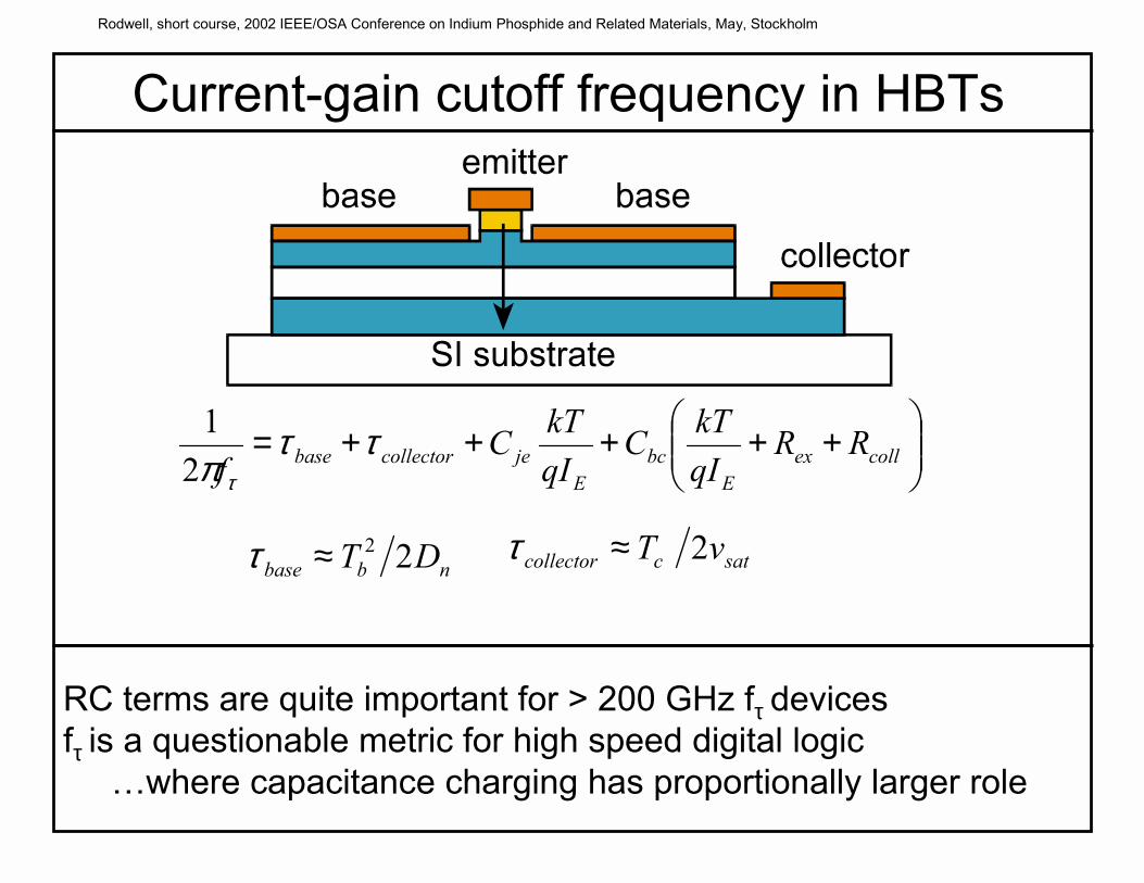
Current-gain cutoff frequency in HBTs
+++++= collex
Ebc
Ejecollectorbase RR
qIkTC
qIkTC
fττ
π τ21
nbbase DT 22≈τ satccollector vT 2≈τ
RC terms are quite important for > 200 GHz fτ devicesfτ is a questionable metric for high speed digital logic
where capacitance charging has proportionally larger role
Rodwell, short course, 2002 IEEE/OSA Conference on Indium Phosphide and Related Materials, May, Stockholm
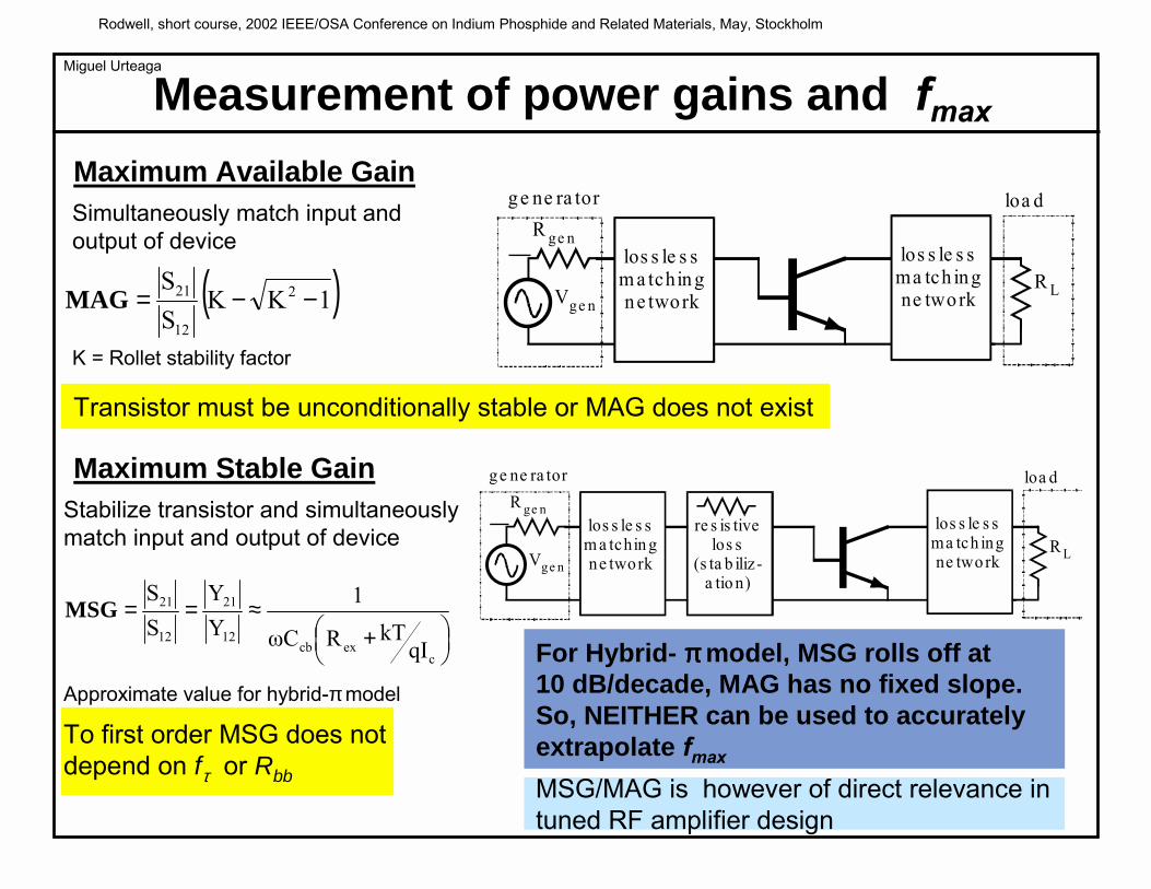
Stabilize transistor and simultaneously match input and output of device
Approximate value for hybrid-πmodel
To first order MSG does not depend on fτ or Rbb
Simultaneously match input and output of device
K = Rollet stability factor
Measurement of power gains and fmax
( )1KKSS 2
12
21 −−=MAG
+
≈==
cexcb
12
21
12
21
qIkTRωC
1YY
SS
MSG
For Hybrid- ππππmodel, MSG rolls off at 10 dB/decade, MAG has no fixed slope.So, NEITHER can be used to accurately extrapolate fmax
Maximum Available Gain
Transistor must be unconditionally stable or MAG does not exist
Maximum Stable Gain
ge ne ra tor
los s le s sm a tchin gne twork
R ge n
Vge n
los s le s sma tch ingne twork
R L
loa d
ge ne ra tor
los s le s sm a tchin gne twork
R ge n
Vge n
los s le s sma tch ingne twork
R L
loa d
re s is tivelos s
(s ta b iliz -a tio n)
Miguel Urteaga
MSG/MAG is however of direct relevance in tuned RF amplifier design

Rodwell, short course, 2002 IEEE/OSA Conference on Indium Phosphide and Related Materials, May, Stockholm
Use lossless reactive feedback to cancel device feedback and stabilize the device, then match input/output.
( )12212211
21221
GGGG4YY−
−=U
Unilateral Power GainMason’s Unilateral Power Gain
0
5
10
15
20
25
30
35
40
1 10 100
Gai
ns, d
B
Frequency, GHz
MAG/MSGcommon base
U: all 3
MAG/MSGcommon collector
MAG/MSGcommon emitter
For Hybrid- ππππmodel, U rolls off at 20 dB/decade
ALL Power Gains must be unity at fmax
U is not changed by pad reactances
g e n e ra to r
lo s s le s sm a tc h in gn e tw o rk
R g e n
Vg e n
lo s s le s sm a tc h in gn e tw o rk
R L
lo a d
s e rie sfe e d b a c k
s h u n tfe e d b a c k
Miguel Urteaga
Monolithic amplifiers not easily made unilateral, so U of only historical relevance to IC design. U is usually valuable for fmax extrapolation

Rodwell, short course, 2002 IEEE/OSA Conference on Indium Phosphide and Related Materials, May, Stockholm
Excess Collector Capacitance, Fmax, and Device Utility
0
5
10
15
20
25
30
35
40
1 10 100
Gai
ns, d
BFrequency, GHz
MAG/MSGcommon base
U: all 3
MAG/MSGcommon collector
MAG/MSGcommon emitter
+
≈==
cex qI
kTRcb12
21
12
21
ωC
1YY
SS
CEMSG
Cbe
Ccbi
Ccbx
gmVbeRbe
RbbB C
E
Rex
Rc
cbibbCRff
πτ
8max ≅
speed. logic digitalupon impact large a has circuits. wave-mmin gain usableon impact large has hence
MSG,emitter -commonupon impact large a has or U. upon effect no has
later. discussed be will and between ngpartitioni The
max
cbx
cbx
cbx
cbxcbi
C
CfC
CC
high fmax does not mean low Ccb or fast logic

Rodwell, short course, 2002 IEEE/OSA Conference on Indium Phosphide and Related Materials, May, Stockholm
Tuned ICs (MIMICs, RF):fmax sets gain,
& max frequency, not ft.low ft/fmax ratio makes tuning design hard (high Q)high Ccbx reduces MSG
What do we need: fτ τ τ τ , fmax , or ?
Lumped analog circuitsneed high & comparable ft and fmax.
Ccb/Ic has major impactupon bandwidth
Distributed Amplifiersin principle, fmax-limited, ft not relevant.(low ft makes design hard)
digital ICs will be discussed in detail later

Rodwell, short course, 2002 IEEE/OSA Conference on Indium Phosphide and Related Materials, May, Stockholm
transistorlayer structures

Rodwell, short course, 2002 IEEE/OSA Conference on Indium Phosphide and Related Materials, May, Stockholm
SHBT layer structure
very low breakdown: scaling beyond ~75 GHz digital clock rate very difficult
high collector-base leakageparticularly at elevated temperatures. Serious difficulties in real applications
very high thermal resistanceInGaAs collector and subcollector
Layer Material Doping Thickness (Å)
Emitter cap In0.53Ga0.47As 2 × 1019 cm-3: Si 300
N+ emitter InP 2 × 1019 cm-3: Si 700
N- emitter InP 8 × 1017 cm-3: Si 500
Emitter-base grade
In0.53Ga0.26Al0.21As to In0.455Ga0.545As
P: 4 × 1017 cm-3: Si N: 8 × 1017 cm-3: C
233 47
Base In0.53Ga0.47As N: 4 × 1019 cm-3: C 400
Collector In0.53Ga0.47As N: 2× 1016 cm-3: Si 2000
Subcollector InP N: 1× 1019 cm-3: Si ~1000 Å

Rodwell, short course, 2002 IEEE/OSA Conference on Indium Phosphide and Related Materials, May, Stockholm
DHBT Layer structure
B-C grade design is critical
InGaAs or GaAsSb bases GaAsSb more easily passivatedotherwise comparable
high breakdownimportant for microwave powerimportant for logic
low thermal resistanceessential for high power density important for microwave powerimportant for logic
Performanceft and fmax good or better than SHBTs
Layer Material Doping Thickness (Å)
Emitter cap In0.53Ga0.47As 2 × 1019 cm-3: Si 300
N+ emitter InP 2 × 1019 cm-3: Si 700
N- emitter InP 8 × 1017 cm-3: Si 500
Emitter-base grade
In0.53Ga0.26Al0.21As to In0.455Ga0.545As
P: 4 × 1017 cm-3: Si N: 8 × 1017 cm-3: C
233 47
Base In0.53Ga0.47As N: 4 × 1019 cm-3: C 400 Base-
collector grade
In0.53Ga0.47As to In0.53Ga0.26Al0.21As N: 2 × 1016 cm-3: Si 240
Pulse doping InP 5.6 × 1018 cm-3: Si 30
Collector InP N: 2× 1016 cm-3: Si 1,630
Subcollector InP N: 1× 1019 cm-3: Si ~1000 Å
emitter
emittercap
gradedbase
collectorsubcollector
PK Sundararajan

Rodwell, short course, 2002 IEEE/OSA Conference on Indium Phosphide and Related Materials, May, Stockholm
Alternative InP DHBT base-collector junction designs
Several layer alternatives exist for DHBTs with:high fthigh current densitynegligible current blockinglow base sheet and contact resistivity
InP collector
InAlAs/InGaAssuperlattice
InGaAssetbackInGaAs
base
UCSB: InGaAs base, MBE
IEDM 2001
Mattias Dahlstrom

Rodwell, short course, 2002 IEEE/OSA Conference on Indium Phosphide and Related Materials, May, Stockholm
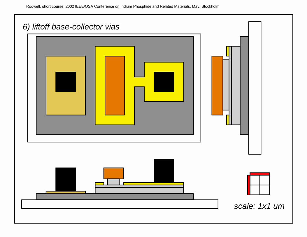
transistorprocess flow(research-lab-like)

Rodwell, short course, 2002 IEEE/OSA Conference on Indium Phosphide and Related Materials, May, Stockholm
scale: 1x1 um
1) emitter metal liftoff

Rodwell, short course, 2002 IEEE/OSA Conference on Indium Phosphide and Related Materials, May, Stockholm
scale: 1x1 um
2) base recess etch

Rodwell, short course, 2002 IEEE/OSA Conference on Indium Phosphide and Related Materials, May, Stockholm
scale: 1x1 um
3) base metal deposition

Rodwell, short course, 2002 IEEE/OSA Conference on Indium Phosphide and Related Materials, May, Stockholm
scale: 1x1 um
4) collector mesa etch

Rodwell, short course, 2002 IEEE/OSA Conference on Indium Phosphide and Related Materials, May, Stockholm
scale: 1x1 um
5) etch through base to subcollector, collector Ohmics
Rodwell, short course, 2002 IEEE/OSA Conference on Indium Phosphide and Related Materials, May, Stockholm
scale: 1x1 um
6) liftoff base-collector vias

Rodwell, short course, 2002 IEEE/OSA Conference on Indium Phosphide and Related Materials, May, Stockholm
scale: 1x1 um
7) planarize: spin on BCB or polyimide & etch back

Rodwell, short course, 2002 IEEE/OSA Conference on Indium Phosphide and Related Materials, May, Stockholm
scale: 1x1 um
8) deposit interconnect metal

Rodwell, short course, 2002 IEEE/OSA Conference on Indium Phosphide and Related Materials, May, Stockholm
Problems with mesa process flowLarge Parasitic Collector Junction, Large Excess Ccbresembles Si bipolar processes of 1960's !parasitic collector junction lies under base contactsbase contacts must be nonzero size: nonzero resistivitybase contacts must be nonzero size: lithographic impact on yield
Self-aligned emitter-base process flowbase-emitter short-circuitsproblems with wet-etch undercut controlproblems with dry-etch reproducibility
Nonplanar processloss of yield in back-end process

Rodwell, short course, 2002 IEEE/OSA Conference on Indium Phosphide and Related Materials, May, Stockholm
scale:1x1 um
emitter-base junction is 3 um^2collector-base junction is 12 um^2
collector/emitter area ratioeven worsein non-self-aligned processes...
Problems with mesa process flow
While research-lab processes have moderate Ccb, processes aimed at high yield at >3000 HBTs have very large collector junctions
Ccb then the dominant circuit parasitic, regardless of impact on fττττ & fmax.

Rodwell, short course, 2002 IEEE/OSA Conference on Indium Phosphide and Related Materials, May, Stockholm
transistorkey parasiticsand model

Rodwell, short course, 2002 IEEE/OSA Conference on Indium Phosphide and Related Materials, May, Stockholm
Emitter Resistance
evidence of edge depletion or damage
( )( )( )WWL
R
WWLR
EcEex
EE
cex
∆−=
∆−=
ρ
ρ
1
?
( )( ) drop voltage excessive high but
low high :devices speedhigh speedfor scalingin factor limiting one :resistanceEmitter
exE
ccb
RIJICJ
→→
Dino Mensa

Rodwell, short course, 2002 IEEE/OSA Conference on Indium Phosphide and Related Materials, May, Stockholm
Current Gain: surface leakage
evidence of surface conduction
Be: InGaAs4E19/cm3 doping
Dino Mensa
Surface Conduction:InGaAs has low surface recombination velocity.InGaAs has surface pinning near conduction band.→ weak surface inversion layer on base, surface conduction to base contactProblem aggravated by InP emitter, as this also pins near conduction band
emitter
base
bulkbnpoE
poE
c
bulk
c
surface
c
b
WDqnAqnkP
II
II
II
β
β1
)/()(
1
1 +=
+==

Rodwell, short course, 2002 IEEE/OSA Conference on Indium Phosphide and Related Materials, May, Stockholm
Current Gain: Auger recombination
ime transit tlow y,resistivitcontact base low basethin doping basehigh But,
doping basehigh through reduction constrains This
1/ )(1
.. 1 Since
1Augerby dominatedion recombinatBulk
feasible cm/10 above :doping baseCarbon
22
2base
2Auger
220
⇒+
∝∝
∝
∝
sheet
sheetBA
B
A
TNT
N
ρ
ρβτ
τ

Rodwell, short course, 2002 IEEE/OSA Conference on Indium Phosphide and Related Materials, May, Stockholm
Base Transit Time
( )( )
( )gbg
g
LWsatgngngbb
EkTWLL
evLDLDLW gb
∆=
−−−= −
/:length grading theis where
1/// /2τ
fs 35/ifcorrect modeldiffusion -Drift
* ≈≈>> kTmDτ nmb τ
cm/s 103
secV/cm 40:Assumes
7
2
⋅=
−=
exit
N
vD
Dino Mensa

Rodwell, short course, 2002 IEEE/OSA Conference on Indium Phosphide and Related Materials, May, Stockholm
Base Bandgap vs. Doping Grading
.resistancesheet degrading without fieldin -built introduceCan
)( maximum sets collapse induced-Auger doping,heavy With
field big induces change doping small :statistics doping Degeneratebase degenerate grading, doping base :3 Case
base of middlein somewhere land contacts :increased resistanceContact resistancesheet base increasedgreatly
1:12.01:by base of sidecollector at doping Reduceyreliabilitgrowth / by dconstraine sideemitter near doping Base
base degenerate-non grading, doping base :2 Case
(strained) AsGaIn AsGaIn :ratio Ga:InVary grading. bandgap base :1 Case
base. across drop potential meV 52 a introduce :Objective
0
2
0.470.530.5450.455
∫
⇒⇒
=
↔
−
bTdxxp
e
β

Rodwell, short course, 2002 IEEE/OSA Conference on Indium Phosphide and Related Materials, May, Stockholm
V=0
TcTc/2
--
+ +
V=0
Tc/4
+ +
--
+ +
----
+
+
Collector Transit TimeT. Ishibashi
base.near velocity tosensitive more is
2)()/1(
sketch) (refer to ticselectrosta elementary From
c
0c
τ
τ ∫ ≡−=CT
eff
cc
vTdx
xvTx
.scattering L- todue decreasesthen high, is velocity initial as ,Fortuitous
Γ

Rodwell, short course, 2002 IEEE/OSA Conference on Indium Phosphide and Related Materials, May, Stockholm
Collector Transit Time
layers A 2000~for cm/s105-3 also collectors InPin Velocities
layers A 2000~for cm/s105-3 collectors InGaAsin Velocities
atad RF fit tobest ...from
7
7
&
&
⋅
⋅
Rodwell, short course, 2002 IEEE/OSA Conference on Indium Phosphide and Related Materials, May, Stockholm
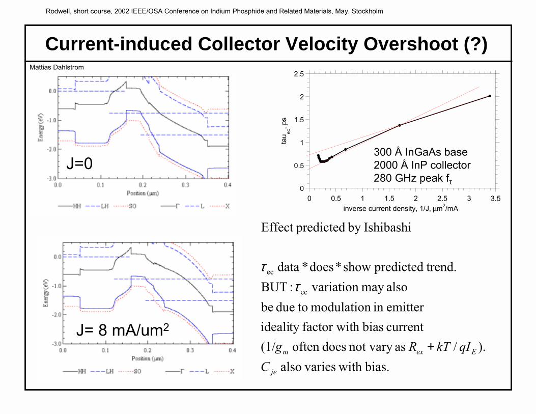
Current-induced Collector Velocity Overshoot (?)
0
0.5
1
1.5
2
2.5
0 0.5 1 1.5 2 2.5 3 3.5
tau ec
, ps
inverse current density, 1/J, µm2/mA
J=0
J= 8 mA/um2
bias. with variesalso )./ asnot vary doesoften (1/
current biash factor witty idealiemitter in modulation todue be
alsomay variation :BUT trend.predicted show *does* data
Ishibashiby predictedEffect
ec
ec
je
Eexm
CqIkTRg +
ττ
Mattias Dahlstrom
300 Å InGaAs base2000 Å InP collector280 GHz peak fτ
Rodwell, short course, 2002 IEEE/OSA Conference on Indium Phosphide and Related Materials, May, Stockholm
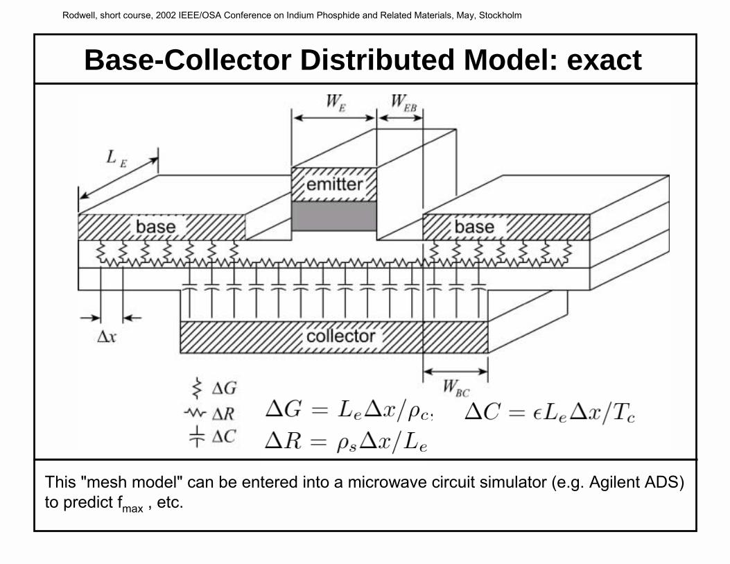
Base-Collector Distributed Model: exact
This "mesh model" can be entered into a microwave circuit simulator (e.g. Agilent ADS)to predict fmax , etc.

Rodwell, short course, 2002 IEEE/OSA Conference on Indium Phosphide and Related Materials, May, Stockholm
Components of Rbb and Ccb
ceeecb TWLC /, ε=
!contcontverthorizx RRRRR =+=
Ebcshoriz LWR 2/ρ=Pulfrey / Vaidyanathan
Miguel Urteaga

Rodwell, short course, 2002 IEEE/OSA Conference on Indium Phosphide and Related Materials, May, Stockholm
Components of base spreading resistance
. negligibleeven with emitters,
narrow with obtained is Low
.length emitter increasedin results dth emitter wi decreased
:fixed is areaemitter Given that
. and by dominated is doping) base 1E20~(or with
emitterssubmicron With
spread
bb
E
E
EEE
gapcontactbb
RR
LW
WLA
RRR
⇒
=

Rodwell, short course, 2002 IEEE/OSA Conference on Indium Phosphide and Related Materials, May, Stockholm
Typical base parameters
(Dvorak)s/cm 20 fs, 200150 ,m-Ohm 20 , eOhms/squar 0001
sA thicknes 250 grading, meV ?? base, GaAsSb doped-C /cm108
s/cm 40 fs, 100 ,m-Ohm 10 , eOhms/squar 700sA thicknes 300 grading, (doping) meV 52 base, InGaAs doped-C /cm107
s/cm 40 fs, 170 ,m-Ohm 100 , eOhms/squar 750sA thicknes 400 grading, meV 52 base, InGaAs doped-Be /cm104
22cs
319
22cs
319
22cs
319
≈−≈≈=
⋅
≈≈<=⋅
≈≈==⋅
nb
nb
nb
D
D
D
τµρρ
τµρρ
τµρρ

Rodwell, short course, 2002 IEEE/OSA Conference on Indium Phosphide and Related Materials, May, Stockholm
Pulfrey / Vaidyanathan fmax model
( )
speed analog and digitaluponimpact bigbut
,upon effect moderate has
small relatively is timecharging associated the...
1
. than less ,resistance low relatively a through charged is
ecapacitanc external that theNote
max,
,,
,
fC
T
RCRRCR
C
extcb
contactc
vertextcbvertcontextcb
vert
extcb
ρε=
<
Pulfrey / Vaidyanathan

Rodwell, short course, 2002 IEEE/OSA Conference on Indium Phosphide and Related Materials, May, Stockholm
Ccb Cancellation by Collector Space-Charge
collector space-charge layer
cbVδ
∂
∂−ε=∂
∂
sat
cc
cbccb
base
vTI
VTA
VQ
2
cb
cc
ccb V
ITAC
∂τ∂−ε=⇒
1.8
2
2.2
2.4
2.6
2.8
0 1 2 3 4 5 6 7
measured0.64 fF decrease
Ccb
tota
l
Ic
Collector space charge screens field, Increasing voltage decreases velocity, → modulates collector space-charge→ offsets modulation of base charge→ Ccb is reduced
Moll & Camnitz, Betser and Ritter
Even if you don't care about fmax,the effect can confuse HBT model extraction

Rodwell, short course, 2002 IEEE/OSA Conference on Indium Phosphide and Related Materials, May, Stockholm
equivalentcircuitmodel

Rodwell, short course, 2002 IEEE/OSA Conference on Indium Phosphide and Related Materials, May, Stockholm
Transistor Hybrid-Pi equivalent circuit model
Cbe
Ccbi
Ccbx
gmVbeRbe
RbbB C
E
Rex
Rc
kTqIg Em /0 =
)( cbmjebe gCC ττ ++=
)(0
cbjmm egg τγτω +−=

Rodwell, short course, 2002 IEEE/OSA Conference on Indium Phosphide and Related Materials, May, Stockholm
Comments regarding the Hybrid-Pi model
networkcollector -base ddistribute theto fitsrepresent and
design) ICfast in (importantdelay )(0.2 ~ associatedan requires also ssneverthelegenerator The
impedanceinput on
)( ofeffect themodels ecapacitanc The
.in order first toT thefit to a from results model pi-hybrid The
transportdependent -frequency modelsdirectly model (T) base-common The
cb
cb,
RCCCR
g
C
cbxcbibb
m
diffbe
ττ
ττ
ω
+⋅
+

Rodwell, short course, 2002 IEEE/OSA Conference on Indium Phosphide and Related Materials, May, Stockholm
Collector field-screening(Kirk Effect)

Rodwell, short course, 2002 IEEE/OSA Conference on Indium Phosphide and Related Materials, May, Stockholm
Kirk effect in DHBTs: not base pushout, but current-blocking
cm/s 104 ,kA/cm 1000 V, 2.1 7,
2 ⋅=== effsatece vJV
cm/s 104 ,kA/cm 0 V, 7.0 7,
2 ⋅=== effsatece vJV
cm/s 104 ,kA/cm 1000 V, 7.0 7,
2 ⋅=== effsatece vJV
τβ
εερφ
f
VJ
vJqNdxd
ce
d
and in decrease
blockingcurrent in results lowand high under gBandbendin
/
2
2
⇒
−==
Mattias Dahlstrom

Rodwell, short course, 2002 IEEE/OSA Conference on Indium Phosphide and Related Materials, May, Stockholm
Kirk effect in DHBTs
0
2
4
6
8
10
12
14
0
1 105
2 105
3 105
4 105
0 1 2 3 4 5 6
Je (A/cm
2 )I C (m
A)
VCE
(V)
0
50
100
150
200
250
0 1 105 2 105 3 105 4 105 5 105 6 105
Cut
off F
requ
enci
es, G
Hz f
τ at V
ce=1.5 V
fmax
at Vce
=1.5 V
Current Density, A/cm2
fmax
at Vce
=0.7 V
fτ at V
ce=0.7 V
ceV
Jff
increasedwith increases esholdeffect thr-Kirk
lower at and in Decrease maxτ
( )CEEeffective
effectivesat
c
c
ce
satce
TWLA
AvTR
dIdV
JV
2is areaflux current
collector effective thewhere2
increased with in Increase2
chargespace
,
+≈
== − ε
2min,
2min,max
/)(2
/)2(2
ccecesat
ccbcbsat
TVVv
TVVvJ
+≅
++=
ε
φε
Young-Min Kim

Rodwell, short course, 2002 IEEE/OSA Conference on Indium Phosphide and Related Materials, May, Stockholm
Kirk effect in SHBTs: base pushout, increased Ccb
increases. electrons compensate Holes
out. pushes Base
cbC
cm/s 103 ,kA/cm 500 V, 7.0 7,
2 ⋅=== effsatece vJV
Base pushes out
Ccb increases Ccb increases

Rodwell, short course, 2002 IEEE/OSA Conference on Indium Phosphide and Related Materials, May, Stockholm
Kirk effect with Nonuniform Collector Electron Velocity
base.near velocity tosensitive more are and
2)()/1(
analysis, ime transit tFrom
c
0c
eff
T
eff
cc
vvTdx
xvTxC
τ
τ ∫ ≡−=
2min,
2min,max
/)(2
/)2(2:velocitycollector uniformh effect witKirk
ccecesat
ccbcbsat
TVVv
TVVvJ
+≅
++=
ε
φε
2min,
2min,max
/)(2
/)2(2:velocitycollector NONuniformh effect witKirk
cceceeff
ccbcbeff
TVVv
TVVvJ
+≅
++=
ε
φε
Nonuniform collector electron velocity doesn't profoundly change Kirk effect

Rodwell, short course, 2002 IEEE/OSA Conference on Indium Phosphide and Related Materials, May, Stockholm
transistorscaling theory
Rodwell, short course, 2002 IEEE/OSA Conference on Indium Phosphide and Related Materials, May, Stockholm
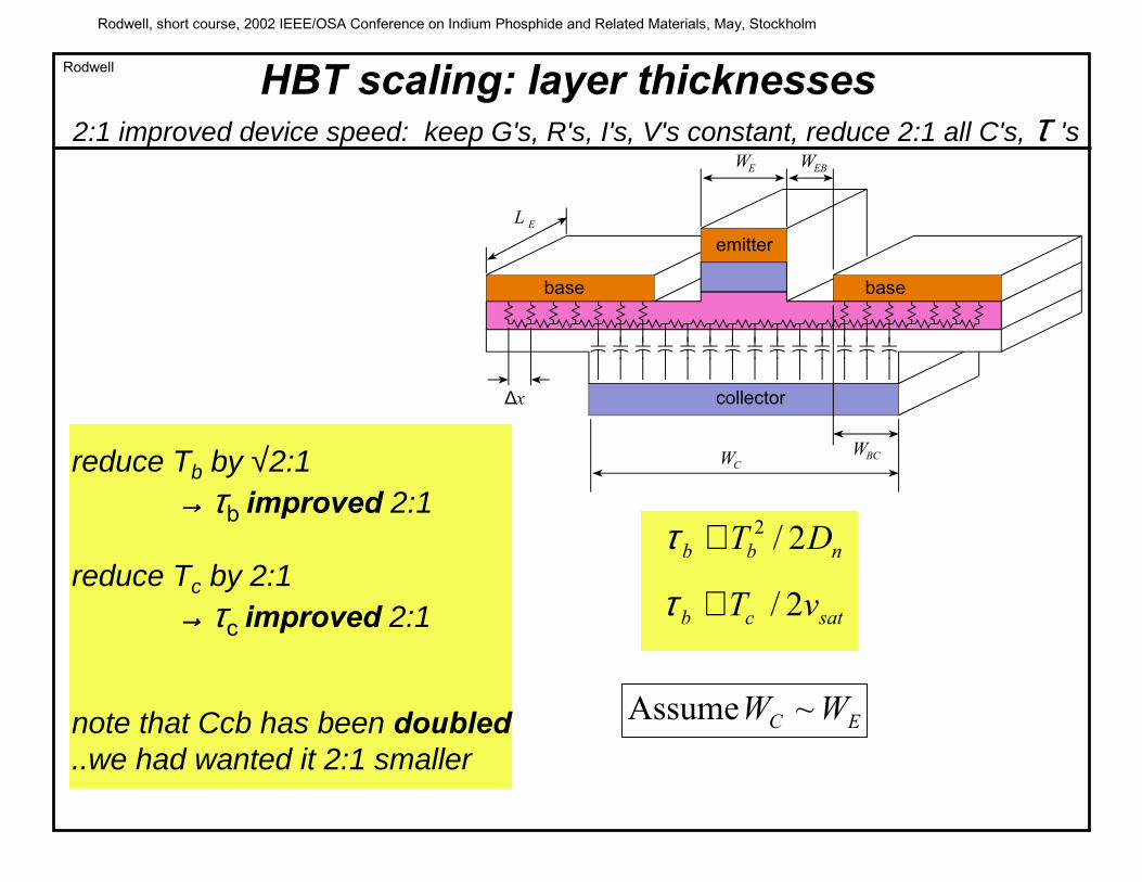
HBT scaling: layer thicknessesWE
WBC
WEB
∆x
L E
base
emitter
base
collector
WCreduce Tb by √2:1→ → → → τb improved 2:1
reduce Tc by 2:1→ → → → τc improved 2:1
note that Ccb has been doubled..we had wanted it 2:1 smaller
nbb DT 2/2≅τ
satcb vT 2/≅τ
2:1 improved device speed: keep G's, R's, I's, V's constant, reduce 2:1 all C's, τ 's
EC WW ~ Assume
Rodwell

Rodwell, short course, 2002 IEEE/OSA Conference on Indium Phosphide and Related Materials, May, Stockholm
HBT scaling: lithographic dimensions
WE
WBC
WEB
∆x
L E
base
emitter
base
collector
WC
Ccb/Area has been doubled..we had wanted it 2:1 smaller…must make area=LeWe 4:1 smaller→ → → → must make We & Wc 4:1 smaller
Everticalcsheet
contact
contactspreadgapbb
L
RRRRR
2,ρρ=
≅
++=Base Resistance Rbb must remain constant→→→→ Le must remain ~ constant
reduce collector width 4:1reduce emitter width 4:1keep emitter length constant
2:1 improved device speed: keep G's, R's, I's, V's constant, reduce 2:1 all C's, τ 's
EC WW ~ Assume
Rodwell

Rodwell, short course, 2002 IEEE/OSA Conference on Indium Phosphide and Related Materials, May, Stockholm
HBT scaling: emitter resistivity, current density
WE
WBC
WEB
∆x
L E
base
emitter
base
collector
WC
Emitter Resistance Rex must remain constantbut emitter area=LeWe is 4:1 smallerresistance per unit area must be 4:1 smaller
increase current density 4:1reduce emitter resistivity 4:1
2:1 improved device speed: keep G's, R's, I's, V's constant, reduce 2:1 all C's, τ 's
Collector current must remain constantbut emitter area=LeWe is 4:1 smallerand collector area=LcWc is 4:1 smallercurrent density must be 4:1 larger
EC WW ~ AssumeRodwell

Rodwell, short course, 2002 IEEE/OSA Conference on Indium Phosphide and Related Materials, May, Stockholm
Scaling Laws, Collector Current Density, Ccb charging time
baseemitter
collector
subcollector
baseemitter
collector
subcollector
Collector Field Collapse (Kirk Effect)
Collector Depletion Layer Collapse
)2/)(/( 2 εφ cdsatcb TqNvJV −+>+
)2/)(( 2min, εφ cTqNV dcb +>+
2min,max /)2(2 ccbcbsat TVVvJ φε ++=⇒
Collector capacitance charging time is reduced by thinning the collector while increasing current
( )( ) ( )
+
∆=∆=∆sat
C
CECE
LOGICCLOGICcCLOGICcb v
TAA
VVVIVTAIVC
2/
emitter
collector
min,collectorε
cecbbe VVV ≅+≅ )( hence , that Note φφ
Rodwell

Rodwell, short course, 2002 IEEE/OSA Conference on Indium Phosphide and Related Materials, May, Stockholm
for x 2 improvement of all parasitics: ft, fmax, logic speed…base √2: 1 thinnercollector 2:1 thinneremitter, collector junctions 4:1 narrowercurrent density 4:1 higheremitter Ohmic 4:1 less resistive
Scaling Laws for fast HBTs
Challenges with Scaling:Collector mesa HBT: collector under base Ohmics. Base Ohmics must be one transfer lengthsets minimum size for collector Emitter Ohmic: hard to improvehow ?Current Density: dissipation, reliabilityLoss of breakdownavalanche Vbr never less than collector Egap (1.12 V for Si, 1.4 V for InP) .sufficient for logic, insufficient for power

Rodwell, short course, 2002 IEEE/OSA Conference on Indium Phosphide and Related Materials, May, Stockholm
digital circuitspeed

Rodwell, short course, 2002 IEEE/OSA Conference on Indium Phosphide and Related Materials, May, Stockholm
10.0
100.0
Dec-80 Dec-85 Dec-90 Dec-95 Dec-00 Dec-05
Divi
der F
requ
ency
(GHz
)
III-V HBTSi BJTSiGe HBTFET/HEMTCMOS
Benchmark: master-slave flip-flop configured as 2:1 static frequency dividerSource: M Sokolich, HRL, Rodwell, UCSB
Logic Speed: III-V vs. Silicon
0.1 um
0.15 um

Rodwell, short course, 2002 IEEE/OSA Conference on Indium Phosphide and Related Materials, May, Stockholm
75 GHz HBT master-slave latchconnected as Static frequency divider
technology:400 Å base, 2000 Å collector HBT0.7 um mask (0.6 um junction) x 12 um emitters1.5 um mask (1.4 um junction) x 14 um collectors
transistor performance:1.8×10⁵ A/cm2 operation, 180 GHz ft, 260 GHz fmaxcollector/ emitter junction area ratio: 2.7:1 (low)Ccb/Ic: 0.9 ps/VRex*I=54 mV
simulations: 95 GHz clock rate in SPICE
UCSBThomas Mathew
Michelle LeeHwe-Jong Kim
-0.14
-0.12
-0.1
-0.08
-0.06
-0.04
-0.02
0
0 50 100 150 200
fin=75GHz, f
out=37.5GHz
Vout
(Vol
ts)
Time(ps)
-0.11
-0.1
-0.09
-0.08
-0.07
-0.06
-0.05
-0.04
-0.03
0 50 100 150 200
fin=69GHz, f
out=34.5GHz
Vout
(Vol
ts)
Time(PS)
modulation is synthesizer 6 GHz subharmonic
3.92 V, 224 mA, 0.88 W
~3.5 dBm input power

Rodwell, short course, 2002 IEEE/OSA Conference on Indium Phosphide and Related Materials, May, Stockholm
Neither fτ nor fmax predicts digital speed
Ccb∆Vlogic/Ic is very important→ collector capacitance reduction is critical→ increased III-V current density is critical
Rex must be very low for low ∆Vlogic at high Jc
InP: Rbb , (τb+τc) , are already low, must remain so
What do we need for fast logic ?
clock clock clock clock
inin
out
outECL M-S latch
( )
( )
( )
+>∆
∆
+
+
+
+
∆
cexLOGIC
LOGIC
Ccb
becb
becbC
LOGIC
IRq
kTV
VIR
CCR
CCI
V
6
leastat bemust swing logic The
resistance base the throughcharge stored
collector base Supplying
resistance base the throughcharging ecapacitancDepletion
swing logic the throughcharging ecapacitancDepletion
:by DeterminedDelay Gate
bb
depletion,bb
depletion,
ττ
Yoram Betser, Raja Pullela

Rodwell, short course, 2002 IEEE/OSA Conference on Indium Phosphide and Related Materials, May, Stockholm
What HBT parameters determine logic speed ?
( )exCicex
bbcbc
cbdiffcbje
RIqkTVRRIV
CCC
+•>∆
+∆
+
/6 as effect,indirect strong very has
from 17% ,)( from 12% ,/ from 68% :imes transit tand sresistanceby Delays Sorting
) (e.g. charging 18%only , charging 38% , charging 44% :escapacitancby Delays Sorting
log
logic ττ
ττ
Caveats: assumes a specific UCSB InP HBT (0.7 um emitter, 1.2 um collector 2kÅ thick, 400 Å base, 1.5E5 A/cm^2)
ignores interconnect capacitance and delay, which is very significant
Cje Ccbx Ccbi (τb+τc) ( I/∆V) total∆V/ I 33.5% 6.7% 27.8% 68.4%∆V/ I 12.3% 12.3%(kT/q) I 1.4% 0.1% 0.4% 0.5% 2.5%Rex -1.3% 0.1% 0.3% 0.9% 0.1%Rbb 10.2% 2.8% 3.7% 16.7%total 43.8% 6.8% 31.3% 17.5% 100.0%
38%
Yoram Betser, Raja Pullela

Rodwell, short course, 2002 IEEE/OSA Conference on Indium Phosphide and Related Materials, May, Stockholm
Logic Speed
Caveat: ignores interconnect capacitance and delay, which is very significant
( )exLOGIC
clock
jiijclockgate
ij
JqkTVf
crafTa
ρ+>∆
Σ==
/6 isswing voltagelogic minimum The frequency.clock maximum theis
where,2/1 form theof isdelay Gate analysis. handby
found flop,-flip slave-master ECLan for tscoefficiendelay eApproximat
max,
Yoram BetserRaja Pullela

Rodwell, short course, 2002 IEEE/OSA Conference on Indium Phosphide and Related Materials, May, Stockholm
Logic Speed: definition of terms
) area"-per" (e.g. areaemitter timesresistanceemitter :) area"-per" (e.g. areaemitter timesresistance base :
swing voltagelogic :areaemitter unit per current emitter :
mestransit ticollector and base of sum :areaemitter unit per ecapacitanc basecollector extrinsic :
areaemitter unit per ecapacitanc basecollector intrinsic :
areaemitter unit per ecapacitancdepletion baseemitter :
exex
bbbb
LOGIC
f
cbx
cbi
je
RRr
VJ
ccc
ρ
τ
∆
Rodwell, short course, 2002 IEEE/OSA Conference on Indium Phosphide and Related Materials, May, Stockholm
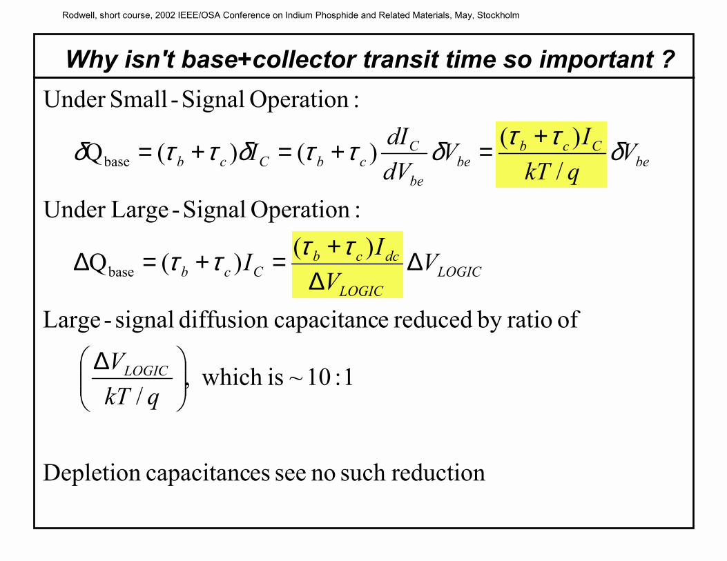
Why isn't base+collector transit time so important ?
reductionsuch no see escapacitancDepletion
1:10~ is which ,/
of ratioby reduced ecapacitancdiffusion signal-Large
)()(Q
:Operation Signal-LargeUnder /
)()()(Q
:Operation Signal-SmallUnder
base
base
∆
∆∆
+=+=∆
+=+=+=
qkTV
VV
II
VqkT
IVdVdII
LOGIC
LOGICLOGIC
dccbCcb
beCcb
bebe
CcbCcb
ττττ
δττδττδττδ

Rodwell, short course, 2002 IEEE/OSA Conference on Indium Phosphide and Related Materials, May, Stockholm
roadmap
Rodwell, short course, 2002 IEEE/OSA Conference on Indium Phosphide and Related Materials, May, Stockholm
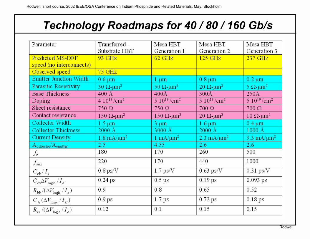
Technology Roadmaps for 40 / 80 / 160 Gb/s
Rodwell

Rodwell, short course, 2002 IEEE/OSA Conference on Indium Phosphide and Related Materials, May, Stockholm
Technology Roadmaps for 40 / 80 / 160 Gb/s
80 Gb/s technology node:Change from 40 Gb/s does not fully follow scaling laws. Why ?Lithographic scaling eased by carbon base doping.Current density scaling eased by reduced excess collector area.
160 Gb/s technology node:Direct application of scaling laws.Aggressive current density and lithographic scaling required.If further improved base contact resistance → relax lithographic scalingFurther reduce Acollector/Aemitter ratio → relax current density scalingnote that Acollector/Aemitter <2.5 looks hard at deep submicron.

Rodwell, short course, 2002 IEEE/OSA Conference on Indium Phosphide and Related Materials, May, Stockholm
device structures

Rodwell, short course, 2002 IEEE/OSA Conference on Indium Phosphide and Related Materials, May, Stockholm
InP mesa HBT
BCB
collector

Rodwell, short course, 2002 IEEE/OSA Conference on Indium Phosphide and Related Materials, May, Stockholm
0.5 µm emitter, 0.25 µm basecontacts
Narrow-Mesa HBTs: high fτ & fmax if high base doping
Mattias Dahlstrom

Rodwell, short course, 2002 IEEE/OSA Conference on Indium Phosphide and Related Materials, May, Stockholm
Low Ccb HBT structures
emitterbase contact
collectorcontact
SI substrate
InGaAs subcollector
InP collector
InGaAscollector
InP subcollector
InGaAs baseundercut
collector junction
Narrow-mesa with ~1E20 carbon-doped base
undercut-collector
transferred-substrate Extremely high demonstrated fmax75 GHz (record) static frequency dividers
Too low yield for manufacturing (?)
Pursued by several research groups
Also has uncertain yield at submicron geometries
The conservative device structure
Yet, I assert that even this device is notviable of mass manufacturing if > 3000 transistors per IC are sought

Rodwell, short course, 2002 IEEE/OSA Conference on Indium Phosphide and Related Materials, May, Stockholm
yield and fabrication

Rodwell, short course, 2002 IEEE/OSA Conference on Indium Phosphide and Related Materials, May, Stockholm
InP HBT limits to yield: non-planar processEmitter contact
Etch to base
Liftoff base metal
Failure modes
Yield degrades as emitters arescaled to submicron dimensions
base contact
emittercontact
base contact
S.I. substrate
base
sub collector
S.I. substrate
base
sub collector
S.I. substrate
base
sub collector
emitter
S.I. substrate
base
sub collector
Emitter planarization, interconnects
base contact
liftoff failure:emitter-baseshort-circuit
S.I. substrate
base
sub collector
base contact
excessiveemitter undercut
S.I. substrate
base
sub collector
S.I. substrate
base
sub collector
planarization failure: interconnect breaks

Rodwell, short course, 2002 IEEE/OSA Conference on Indium Phosphide and Related Materials, May, Stockholm
InP
Front and side views
InAlAs
Front and side views
0.7 um
0.5 um metal~0.4 um junction
0.6 um metal~0.4 um junction
Smaller emitters → lower yield. Need better fabrication process
Rodwell, short course, 2002 IEEE/OSA Conference on Indium Phosphide and Related Materials, May, Stockholm
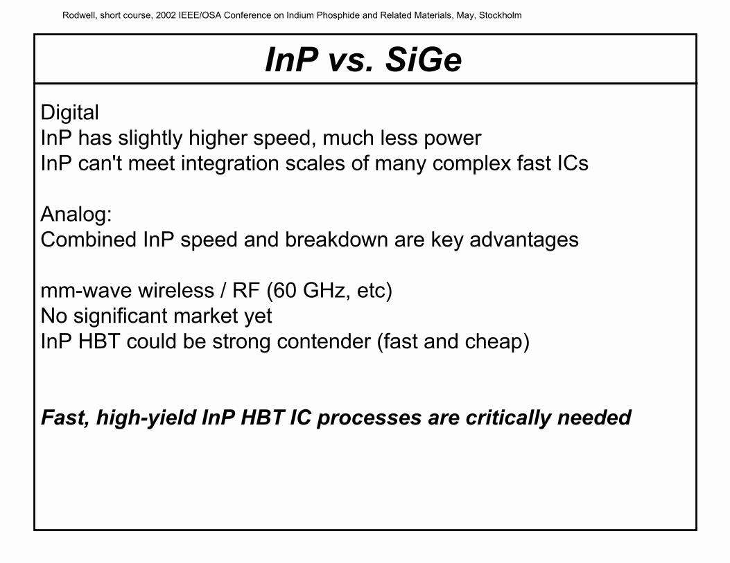
InP vs. SiGe Digital InP has slightly higher speed, much less powerInP can't meet integration scales of many complex fast ICs
Analog:Combined InP speed and breakdown are key advantages
mm-wave wireless / RF (60 GHz, etc)No significant market yetInP HBT could be strong contender (fast and cheap)
Fast, high-yield InP HBT IC processes are critically needed

Rodwell, short course, 2002 IEEE/OSA Conference on Indium Phosphide and Related Materials, May, Stockholm
InP vs. SiGe III-V literature, III-V research community:large inherent advantages in transport parameters over Siresearch focused on transport physics, poorly tied to circuit design→ → → → devices not well-tuned for circuits, poor parasitic reduction → → → → university-like fabrication, low yield, low scales of integration
Silicon research communityfocused on SCALING, closely tied to circuit design, focus on YEILDstrong extrinsic parasitic reductionresult: very good SiGe HBT digital circuit speed, large fast ICs
InP HBT has fundamental advantages which will allow it to scale beyond SiGe HBT scaling limits, but must address:
yield: Silicon-like planar implanted / regrowth processesspeed: device scaling informed by understanding of circuit design

Rodwell, short course, 2002 IEEE/OSA Conference on Indium Phosphide and Related Materials, May, Stockholm
InP vs. Si/SiGe HBTs: materials vs. scaling advantagesGood:Narrow emitter: 0.18 um High current density: 10 mA/um2
Large emitter contact: low resistancePolysilicon base contact: low resistance SiO2 trenches: small collector capacitancePlanar device : high yieldBad:High base sheet resistance, Low electron velocity, low breakdown limits scaling.Equal speed at 5x smaller scaling.Loss of breakdown may soon slow scaling
Good:20x lower base sheet resistance, 5 x higher electron velocity, 4x higher breakdown-at same ft.
Bad:Presently only scaled to ~ 1 umArchaic mesa fabrication process:
large emitters, poor emitter contact:low current density: 2 mA/um2
high collector capacitance nonplanar device : low yield

Rodwell, short course, 2002 IEEE/OSA Conference on Indium Phosphide and Related Materials, May, Stockholm

Rodwell, short course, 2002 IEEE/OSA Conference on Indium Phosphide and Related Materials, May, Stockholm
InAlAs/InGaAs/InP DHBT with polycrystalline extrinsic emitter regrowth.
emitterbase
collector
poly-InAsextrinsic emitter
subcollector
UCSBDennis Scott
ONR

Rodwell, short course, 2002 IEEE/OSA Conference on Indium Phosphide and Related Materials, May, Stockholm
thermal resistance andthermal runaway

Rodwell, short course, 2002 IEEE/OSA Conference on Indium Phosphide and Related Materials, May, Stockholm
Thermal resistance and effect of subcollector
collector
BInPB
B
BInPBBInGaAs
InGaAs
EEInP
cInPJA LKW
LLKLWK
TLWK
Tππ
θ 1ln12/, +
++≈
LB
WBApproximation:InGaAs dominates thermal resistance → heat flows through InGaAs in areaequal base mesa (excluding pad)
m- W/k68 m- W/k5V 1.2 ,mmA/ 4
m, 25.3 m, 7.0 m, 3 m, 5.02
====
====
InPInGaAs
CEE
EBEE
KKVJ
LWLWµ
µµµµ
7 127 16 117 13 16 11
∆T, 2000 Å InGaAs
∆T, 200 Å InGaAs
InGaAs subcollector
W. Liu, H-F Chau, E. Beam III, "Thermal properties and thermal instabilities of InP-based heterojunction bipolar transistors", IEEE Transactions on Electron Devices, vol.43, (no.3), IEEE, March 1996. p.388-95.

Rodwell, short course, 2002 IEEE/OSA Conference on Indium Phosphide and Related Materials, May, Stockholm
8 finger common emitter DHBTEmitter size: 16 um x 1 um Ballast resistor (design):9 Ohm/finger
0
20
40
60
80
100
120
0 1 2 3 4 5
I c, mA
Vce
, Volts
Ibstep = 380 µA
0
5
10
15
20
25
0 1 2 3 4 5 6
I c, mA
Vce
, Volts
Ibstep = 300 µA
0
5
10
15
20
25
1010 1011
Gai
ns, d
B
Frequency, Hz
H21
U
fmax
=120 GHz
fτ=91 GHz
Jc=5e4 A/cm2
Vce=1.5 V
Poor performance observed in multi-finger DHBT
current hogging observedfmax also low due to high
base feed resistance
UCSBYun Wei
ARO MURI
W. Liu, H-F Chau, E. Beam III, "Thermal properties and thermal instabilities of InP-based heterojunction bipolar transistors", IEEE Transactions on Electron Devices, vol.43, (no.3), IEEE, March 1996. p.388-95.

Rodwell, short course, 2002 IEEE/OSA Conference on Indium Phosphide and Related Materials, May, Stockholm
Excess Rbb, hence reduced fmax (big HBT has big Ccb, small Rbb, hence even small excess Rbb reduces fmax)
base
emitter
base feed-in contact
Restrictions on DHBT sizing: distributed base feed resistance
base contact
Self-aligned base contact thickness=0.08 µmLeads to feed sheet resistance:ρ = 0.3 Ω/restricts emitter length to ~15 µm
UCSBYun Wei
ARO MURI

Rodwell, short course, 2002 IEEE/OSA Conference on Indium Phosphide and Related Materials, May, Stockholm
DHBT thermal stability: multiple emitter fingers UCSBYun Wei
ARO MURI
1/
unless Unstable
/
1
constant at mV/K 1.1
fingers 2between difference re temperatuinitial Assume
stability thermal <++
=
=⇒=⇒++
=⇒=⇒
−=
Eballastex
JACEbe
JACCE
beEballastex
Cbe
be
cbe
qIkTRRV
dTdVK
PTIVP
VqIkTRR
ITdT
dVVT
IdT
dVT
θ
δθδδδ
δδδδδ
δ
W. Liu, H-F Chau, E. Beam III, "Thermal properties and thermal instabilities of InP-based heterojunction bipolar transistors", IEEE Transactions on Electron Devices, vol.43, (no.3), IEEE, March 1996. p.388-95.

Rodwell, short course, 2002 IEEE/OSA Conference on Indium Phosphide and Related Materials, May, Stockholm
With long emitter finger, current-crowding can occur within finger Long finger: temperature can vary along length of emitter finger
loss of strong thermal couplingTemperature gradients along finger results in nonuniform current distribution
center of stripe gets hotter → carries more current → gets hotter → Premature Kirk-effect-induced collapse in ft.
Thermal runaway within a finger UCSBYun Wei
ARO MURI
emitter

Rodwell, short course, 2002 IEEE/OSA Conference on Indium Phosphide and Related Materials, May, Stockholm
0
0.01
0.02
0.03
0.04
0.05
0 0.5 1 1.5 2
I_DC
SRC1
I_Probe
I_Probe1
I_Probe
I_Probe2
V_DC
SRC2
Current hogging observation: multi-finger DHBT UCSBYun Wei
ARO MURI
W. Liu, H-F Chau, E. Beam III, "Thermal properties and thermal instabilities of InP-based heterojunction bipolar transistors", IEEE Transactions on Electron Devices, vol.43, (no.3), IEEE, March 1996. p.388-95.
Rodwell, short course, 2002 IEEE/OSA Conference on Indium Phosphide and Related Materials, May, Stockholm
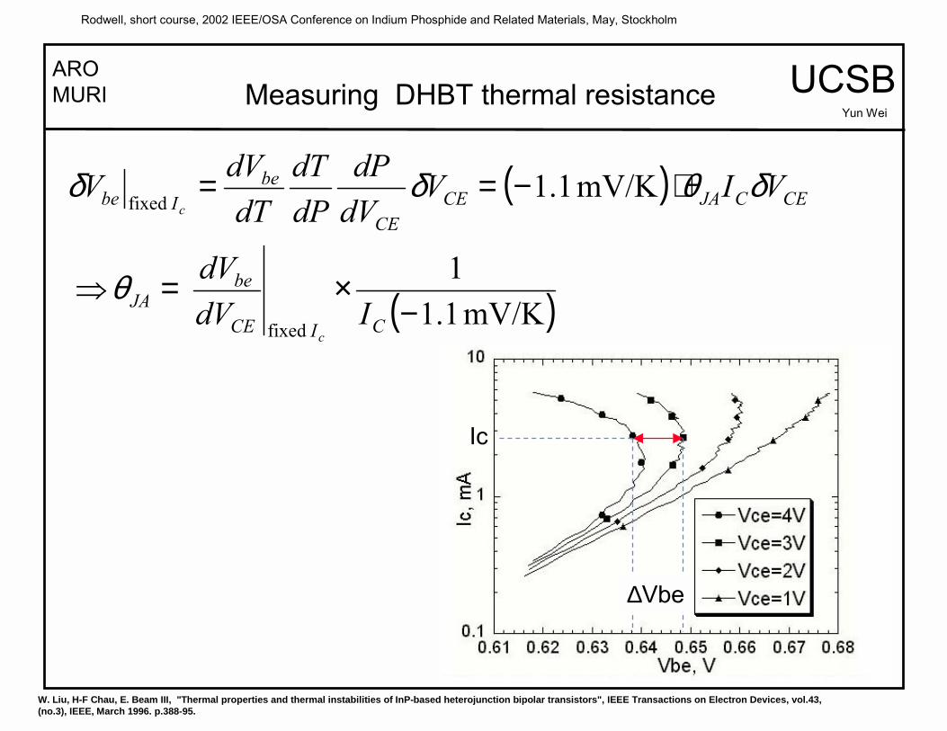
Measuring DHBT thermal resistance
∆Vbe
Ic
UCSBYun Wei
ARO MURI
( )
( )mV/K 1.11
mV/K 1.1
fixed
fixed
−×=⇒
⋅−==
CICE
beJA
CECJACECE
beIbe
IdVdV
VIVdVdP
dPdT
dTdVV
c
c
θ
δθδδ
W. Liu, H-F Chau, E. Beam III, "Thermal properties and thermal instabilities of InP-based heterojunction bipolar transistors", IEEE Transactions on Electron Devices, vol.43, (no.3), IEEE, March 1996. p.388-95.

Rodwell, short course, 2002 IEEE/OSA Conference on Indium Phosphide and Related Materials, May, Stockholm
Large current high breakdown voltage broadband InP DHBT
Objectives: fmax>300 GHz, BVCEO>6 V, Jmax~1x10⁵ A/cm2
Approach: transferred-substrate multi-finger InP DHBTs, HBT thermal analysis
Simulations: large signal HBT spice model
Accomplishments:fmax>330 GHz, Bvce>7 V, Jmax>1x10⁵ A/cm2
UCSBYun Wei
128 µµµµm2 common base DHBT
0
20
40
60
80
100
120
140
0 2 4 6 8 10
Ic, m
A
Vcb, V
AE=128 um2
0
2
4
6
8
10
12
14
-1 0 1 2 3 4 5 6 7
Ic, m
A
Vcb, V0
5
10
15
20
25
30
100 101 102 103
U, M
SG/M
AG, d
B
Frequency, GHz
MSG/MAGU
fmax=330 GHz
AE=128um2
IC=100mAVcb=2.9V
ARO MURI

Rodwell, short course, 2002 IEEE/OSA Conference on Indium Phosphide and Related Materials, May, Stockholm
On-wafercharacterizationof HBTs
accurate andotherwise
Rodwell, short course, 2002 IEEE/OSA Conference on Indium Phosphide and Related Materials, May, Stockholm
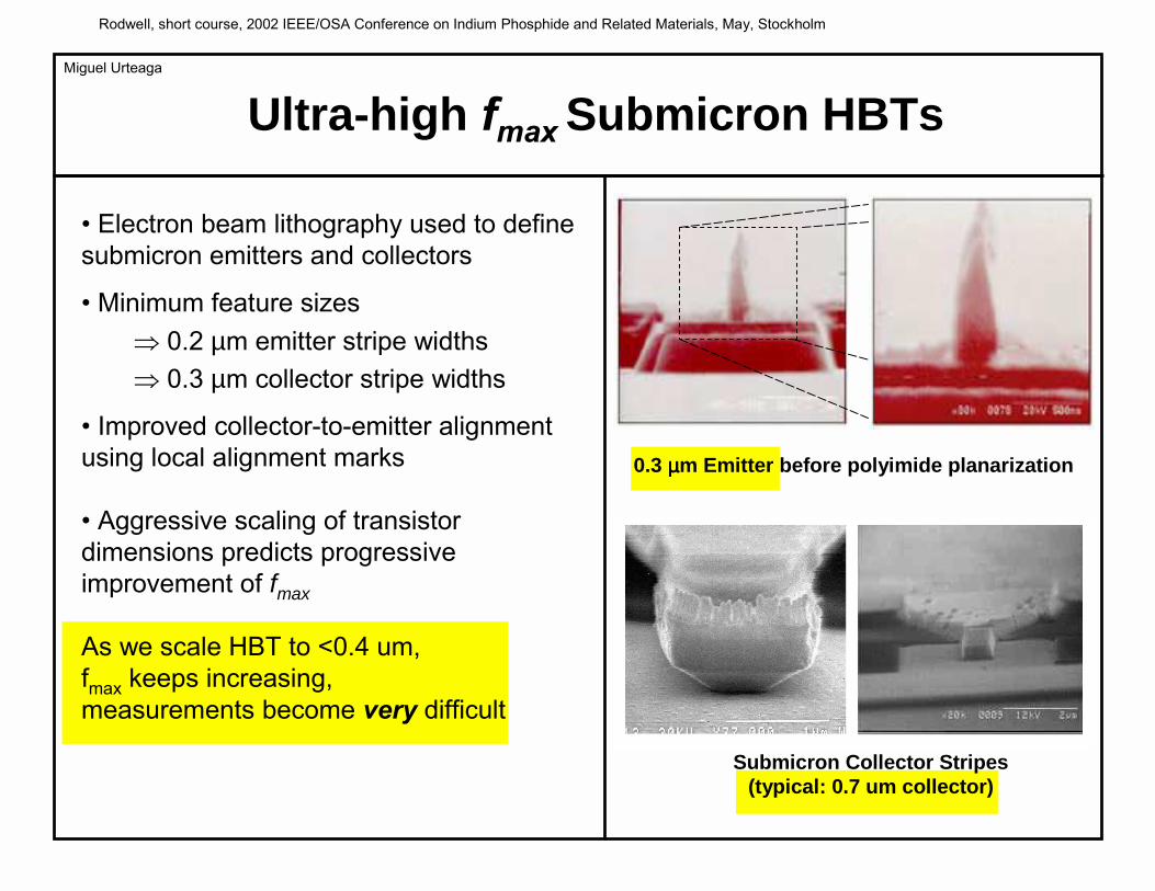
Ultra-high fmax Submicron HBTs
Electron beam lithography used to define submicron emitters and collectors
Minimum feature sizes⇒ 0.2 µm emitter stripe widths ⇒ 0.3 µm collector stripe widths
Improved collector-to-emitter alignment using local alignment marks
Aggressive scaling of transistor dimensions predicts progressive improvement of fmax
As we scale HBT to <0.4 um,fmax keeps increasing,measurements become very difficult
0.3 µµµµm Emitter before polyimide planarization
Submicron Collector Stripes(typical: 0.7 um collector)
Miguel Urteaga

Rodwell, short course, 2002 IEEE/OSA Conference on Indium Phosphide and Related Materials, May, Stockholm
HP8510C VNA, Oleson Microwave Lab mm-wave Extenders
GGB Industries coplanar wafer probes
connection via short length of WR-5 waveguide
Internal bias Tees in probes for biasing active devices
75-110 GHz set-up is similar
140-220 GHz On-Wafer Network Analysis
UCSB 140-220 GHz VNA Measurement Set-up

Rodwell, short course, 2002 IEEE/OSA Conference on Indium Phosphide and Related Materials, May, Stockholm
0
5
10
15
20
25
30
35
1 10 100Frequency, GHz
MSG
h21
Mason'sGain, U
Submicron HBTs have very low Ccb (< 3 fF) Characterization requires accurate measure of very small S12 Standard 12-term VNA calibrations do not correct S12 background error due to probe-to-probe coupling
SolutionEmbed transistors in sufficient length of transmission line to reduce coupling
Place calibration reference planes at transistor terminals
Line-Reflect-Line CalibrationStandards easily realized on-wafer
Does not require accurate characterization of reflect standards
Characteristics of Line Standards are well controlled in transferred-substrate microstrip wiring environment
Accurate Transistor Measurements Are Not Easy
Transistor in Embedded in LRL Test Structure
230 µm 230 µm
Corrupted 75-110 GHz measurements due toexcessive probe-to-probe coupling
Miguel Urteaga

Rodwell, short course, 2002 IEEE/OSA Conference on Indium Phosphide and Related Materials, May, Stockholm
140 150 160 170 180 190 200 210 220
freq, GHz
-0.15
-0.10
-0.05
0.00
0.05
0.10
0.15
0.20
0.25
0.30
freq (75.00GHz to 110.0GHz)
Can we trust the calibration ?
freq (140.0GHz to 220.0GHz)
S11 of throughAbout 40 dB
140-220 GHz calibration looks OK75-110 GHz calibration looks Great
S11 of openAbout 0.1 dB / 3o error
dBS21 of through line is off by less than 0.05 dB
S11 of openS11 of short S11 of through
75 80 85 90 95 100 105 110
freq, GHz
-70
-65
-60
-55
-50
-45
-40
Probe-Probe couplingis better than 45 dB
Miguel Urteaga

Rodwell, short course, 2002 IEEE/OSA Conference on Indium Phosphide and Related Materials, May, Stockholm
140-220 GHz Calibration Verification:Measurement of Thru Line after Calibration
S11, S22 (dB)
Magnitude S21 (dB) Phase S21 (degrees)
Miguel Urteaga

Rodwell, short course, 2002 IEEE/OSA Conference on Indium Phosphide and Related Materials, May, Stockholm
transistorresults

Rodwell, short course, 2002 IEEE/OSA Conference on Indium Phosphide and Related Materials, May, Stockholm
Ultra-high fmax Transferred-Substrate HBTs Substrate transfer provides access to both sides of device epitaxy
Permits simultaneous scaling of emitter and collector widths
Maximum frequency of oscillation
⇒
Sub-micron scaling of emitter and collector widths has resulted in record values of extrapolated fmax
Extrapolation begins where measurements end
New 140-220 GHz Vector Network Analyzer (VNA) extends device measurement range 0
5
10
15
20
25
30
10 100 1000
Gai
ns, d
B
Frequency, GHz
fmax= 1.1 THz ??fτ
= 204 GHz
Mason's gain, U
H21
MSG
Emitter, 0.4 x 6 µm2
Collector, 0.7 x 6 µm2
Ic
= 6 mA, Vce
= 1.2 V
3000 Å collector400 Å base with 52 meV gradingAlInAs / GaInAs / GaInAs HBT
cbbbCRff πτ 8/max ≅
Michelle Lee
Rodwell, short course, 2002 IEEE/OSA Conference on Indium Phosphide and Related Materials, May, Stockholm
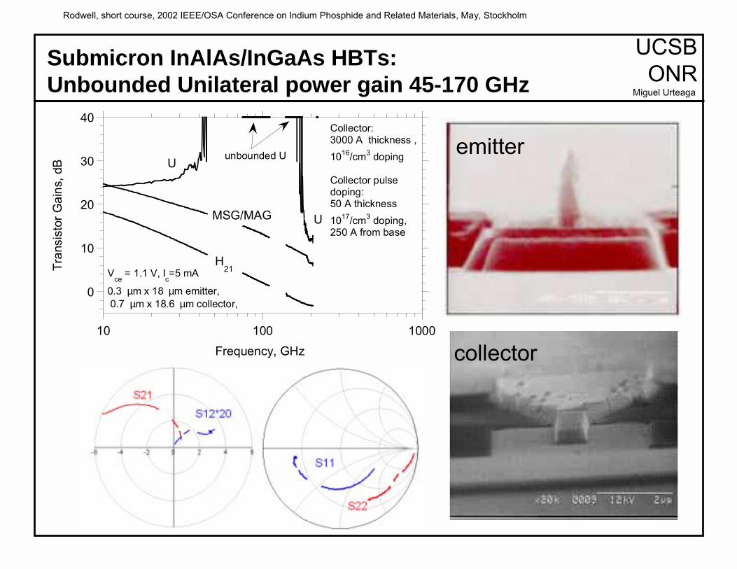
Submicron InAlAs/InGaAs HBTs: Unbounded Unilateral power gain 45-170 GHz
UCSBONR
emitter
collector
Miguel Urteaga
0
10
20
30
40
10 100 1000
Tran
sist
or G
ains
, dB
Frequency, GHz
U
UMSG/MAG
H21
unbounded U
Collector: 3000 A thickness , 1016/cm3 doping
Collector pulse doping: 50 A thickness 1017/cm3 doping, 250 A from base
Vce
= 1.1 V, Ic=5 mA
0.3 µm x 18 µm emitter, 0.7 µm x 18.6 µm collector,
Rodwell, short course, 2002 IEEE/OSA Conference on Indium Phosphide and Related Materials, May, Stockholm
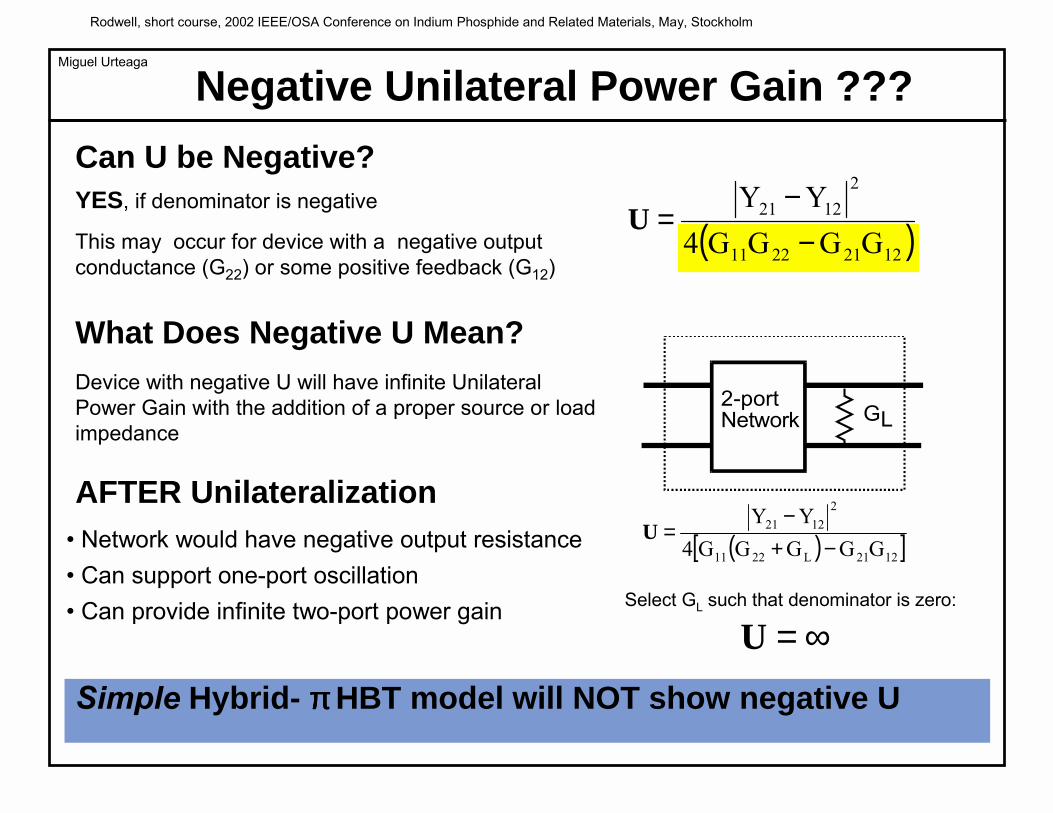
Negative Unilateral Power Gain ???
YES, if denominator is negative
This may occur for device with a negative output conductance (G22) or some positive feedback (G12)
( )12212211
21221
GGGG4YY−
−=U
( )[ ]1221L2211
21221
GGGGG4YY
−+−
=U
2-portNetwork GL
Select GL such that denominator is zero:
Can U be Negative?
What Does Negative U Mean?Device with negative U will have infinite Unilateral Power Gain with the addition of a proper source or load impedance
AFTER Unilateralization Network would have negative output resistance Can support one-port oscillation Can provide infinite two-port power gain
∞=USimple Hybrid- ππππ HBT model will NOT show negative U
Miguel Urteaga

Rodwell, short course, 2002 IEEE/OSA Conference on Indium Phosphide and Related Materials, May, Stockholm
DC-200 GHz parameters of 0.3 µm Emitter / 0.7 µm Collector HBTs:
0 100
2 10-15
4 10-15
6 10-15
8 10-15
1 10-14
0 50 100 150 200
Ic = 1 mAIc = 2 mAIc = 3 mAIc = 4 mAIc = 5 mA
Cc
(Far
ads)
Frequency (GHz)
Vce
=1.2 V
-1 10-3
0 100
1 10-3
2 10-3
3 10-3
4 10-3
5 10-3
0 50 100 150 200
Ic = 1 mAIc = 2 mAIc = 3 mAIc = 4 mAIc = 5 mA
Gc
(S)
Frequency (GHz)
Vce
=1.2 V
-1
-0.5
0
0.5
1
0 50 100 150 200
magnitudereal partimaginary part
Frequency (GHz)
Com
mon
-bas
e cu
rrent
gai
n, a
lpha
Vce
=1.2 V
Ic=5 mA
0
2
4
6
8
10
0
2
4
6
8
10
0 0.5 1 1.5 2 2.5
1/2πft, 0.3 µm x 18 µm emitter
1/2πft, 0.4 µm x 6 µm emitter
Ccb
, 0.3 µm x 18 µm emitter
Ccb
, 0.4 µm x 6 µm emitter
Collector-base capacitance C
cb , fF
Inverse of collector current, Ic (1/mA)
Ic= 5 mA
Ic= 6 mA
No evidence whatsoever of the postulated base pushout phenomenon of Jäckel et al(this theory also uses an erroneous hole mobility, error due to calculus derivatives chain rule error)
Miguel Urteaga

Rodwell, short course, 2002 IEEE/OSA Conference on Indium Phosphide and Related Materials, May, Stockholm
0.0
1.0
2.0
3.0
4.0
5.0
6.0
0 0.5 1 1.5 2 2.5 3
Vce(V)
Ic(m
A)
transferred-substrate DHBTs UCSBSangmin Lee
0.0
1.0
2.0
3.0
0 1 2 3 4 5 6 7 8 9
Vce(V)
Ic(m
A)
BVCEO = 8 V at JE =0.4 mA/µm2
0
5
10
15
20
25
30
35
1.E+09 1.E+10 1.E+11 1.E+12
Frequency (Hz)
h21,
U (d
B)
fmax = 425 GHz, ft = 139 GHz
0.4 µm x 8 µm emitter 1.2 µm x 8.75 µm collectorIc=4.5 mA, Vce=1.9 V
Vce(sat) ~1 V at 1.8 mA/µm2
much wider bandwidth devices coming soon (we hope…)

Rodwell, short course, 2002 IEEE/OSA Conference on Indium Phosphide and Related Materials, May, Stockholm
Wideband Mesa InP/InGaAs/InP DHBTsWalsin
ONRUCSB IQEMattias Dahlstrom / Amy Liu
We have obtained high ft and very high fmaxin mesa DHBTs with C-doped InGaAs bases
Devices have very narrow base mesas and extremely low base contact resistivity
Unlike transferred-substrate HBTs, whichhave very low Ccbx , these devices have significant extrinsic collector-base junction areas.
→ further effort needed in excess Ccb reduction for >100 GHz digital ICs
Results to be presented soon
Rodwell, short course, 2002 IEEE/OSA Conference on Indium Phosphide and Related Materials, May, Stockholm
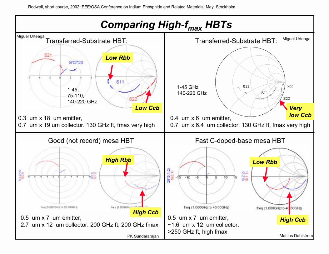
Comparing High-fmax HBTsMiguel Urteaga
S11
S22
S22
S111-45, 75-110, 140-220 GHz
Transferred-Substrate HBT:
0.3 um x 18 um emitter,0.7 um x 19 um collector. 130 GHz ft, fmax very high
Transferred-Substrate HBT:
0.4 um x 6 um emitter,0.7 um x 6.4 um collector. 130 GHz ft, fmax very high
Good (not record) mesa HBT
0.5 um x 7 um emitter,2.7 um x 12 um collector. 200 GHz ft, 200 GHz fmax
Miguel Urteaga
Fast C-doped-base mesa HBT
0.5 um x 7 um emitter,~1.6 um x 12 um collector. >250 GHz ft, high fmax
Verylow Ccb
Low Rbb
High Ccb
Mattias DahlstromPK Sundararajan
Low Rbb
Low Ccb
High Rbb
High Ccb
1-45 GHz, 140-220 GHz

Rodwell, short course, 2002 IEEE/OSA Conference on Indium Phosphide and Related Materials, May, Stockholm
InP/InGaAs/InP Metamorphic DHBTon GaAs substrate UCSB
triple-mesa device(not transferred-substrate)
Growth:400 Å base, 2000 Å collectorGaAs substrateInP metamorphic buffer layer
(high thermal conductivity)Processing
conventional mesa HBTnarrow 2 um base mesa, 0.4 um emitter
Results207 GHz ft, 140 GHz fmax, >6 Volt BVCEO, β=76
Young-Min Kim
0
10
20
30
40
0.1 1 10 100 1000frequency (GHz)
h21
U
ft = 207 GHz
fmax
= 140 GHz
0
2
4
6
8
10
12
14
0
1 105
2 105
3 105
4 105
0 1 2 3 4 5 6
J (A/cm2 )I C
(mA)
VCE
(V)

Rodwell, short course, 2002 IEEE/OSA Conference on Indium Phosphide and Related Materials, May, Stockholm
IC results

Rodwell, short course, 2002 IEEE/OSA Conference on Indium Phosphide and Related Materials, May, Stockholm
75 GHz HBT master-slave latchconnected as Static frequency divider
technology:400 Å base, 2000 Å collector HBT0.7 um mask (0.6 um junction) x 12 um emitters1.5 um mask (1.4 um junction) x 14 um collectors1.8×105 A/cm2 operation, 180 GHz ft, 260 GHz fmax
simulations: 95 GHz clock rate in SPICE
test data to date:tested, works over full 26-40 and 50-75 GHz bands
UCSBThomas Mathew
Michelle LeeHwe-Jong Kim
-0.14
-0.12
-0.1
-0.08
-0.06
-0.04
-0.02
0
0 50 100 150 200
fin=75GHz, f
out=37.5GHz
Vout
(Vol
ts)
Time(ps)
-0.11
-0.1
-0.09
-0.08
-0.07
-0.06
-0.05
-0.04
-0.03
0 50 100 150 200
fin=69GHz, f
out=34.5GHz
Vout
(Vol
ts)
Time(PS)
modulation is synthesizer 6 GHz subharmonic
3.92 V, 224 mA, 0.88 W
~3.5 dBm input power

Rodwell, short course, 2002 IEEE/OSA Conference on Indium Phosphide and Related Materials, May, Stockholm
18 GHz Σ−∆ ADC
Designcomparator is 75 GHz flip flopDC bias provided through 1 KΩ resistors Integration obtained with 3 pF capacitors RTZ gated DAC
Integrated Circuit150 HBTs, 1.2 x 1.5 mm, 1.5 W
gm2
Bias
Bias
C
C
Rz
Rz
Integrator-1 Integrator-2Bias
Bias
C
C
Master-Slave
Flip-flop
Clock
Out
Idac
gm1
DelayedClock
Vin
CurrentSumming
node
RL
RLRL
RL
UCSBS Jaganathan

Rodwell, short course, 2002 IEEE/OSA Conference on Indium Phosphide and Related Materials, May, Stockholm
High Speed Amplifiers
18 dB, DC--50+ GHz
UCSBDino Mensa
PK Sundararajan
8.2 dB, DC-80 GHz
-15
-10
-5
0
5
10
0 10 20 30 40 50 60 70 80
Gai
ns, d
B
Frequency, GHz
S21
S11
S22
-20
-15
-10
-5
0
5
10
15
20
0 10 20 30 40 50
>397 GHzgain x bandwidth from 2 HBTs
S22
S11
S21

Rodwell, short course, 2002 IEEE/OSA Conference on Indium Phosphide and Related Materials, May, Stockholm
HBT distributed amplifier UCSBPK Sundararajan11 dB, DC-87 GHz
AFOSR
-20
-15
-10
-5
0
5
10
15
0 20 40 60 80
Gai
ns, d
B
Frequency, GHz
S21
S22
S11
TWA with internal ft-doubler cells

Rodwell, short course, 2002 IEEE/OSA Conference on Indium Phosphide and Related Materials, May, Stockholm
175 GHz Single-Stage AmplifierSubmicron HBT Program
UCSBMiguel Urteaga
-20
-15
-10
-5
0
5
10
140 150 160 170 180 190 200 210 220
S21S11S22
dB
Freq. (GHz)
0.2pF
50Ω 30Ω,1.2ps
50Ω
30Ω,0.2ps
80Ω,1.2ps
30Ω,0.6ps
80Ω,1.2ps
50Ω
IN
OUT
6.3 dB gain at 175 GHz

Rodwell, short course, 2002 IEEE/OSA Conference on Indium Phosphide and Related Materials, May, Stockholm
40 mW, W-band InP DHBT power amplifiers
Objectives: W band, P1dB>9 dBm, Psat>12 dBm
Approach: transferred-substrate InP DHBTs, microwave amplifier design
Simulations: S-parameter and harmonic simulation in ADS
Accomplishments:f0=85 GHz, BW3dB=28 GHz,
GT=8.5 dB, P1dB=14.5 dBm, Psat=16dBm
UCSBYun Wei
common base PA
-5
0
5
10
15
20
0
2
4
6
8
10
-15 -10 -5 0 5 10 15
Pout
, dBm G
T , dB
Pin, dBm
GT Pout
-30
-25
-20
-15
-10
-5
0
5
10
80 90 100 110
S11
, S21
, S22
frequency, GHz
S21
S22
S11
0.5mm x 0.4 mm, AE=128 µµµµm2
ARO MURI