integrated inductors with magnetic materials for on-chip ......• inductors with magnetic material...
TRANSCRIPT

Integrated Inductors with Magnetic Materials for On-Chip Power Conversion
Donald S. GardnerCollaborators: Gerhard Schrom, Fabrice Paillet,
Tanay Karnik, Shekhar Borkar
Circuits Research Lab & Future Technology Research
Intel LabsIntel Corporation

Outline• DC Voltage Converters
– Comparison of buck converters– Comparison of inductors with magnetic films
• Magnetic material properties– Magnetic hysteresis loops – Complex permeability spectra
• Inductors– Structure cross sections– Inductance measurements– Eddy current and skin effect– Sheet and shunt inductance

Multi -Core Power Management
• Today - Coarse Grain Power Management– same voltage to all the cores, variable voltage
• Future – Fine Grain Power Management– each core or cluster of cores operates at the
optimum voltage
Voltage RegulatorVoltage Regulator
Voltage RegulatorVoltage Regulator
Voltage Regulator
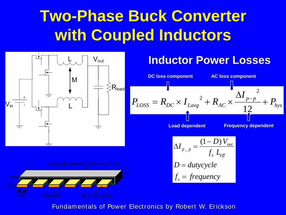
Two-Phase Buck Converter with Coupled Inductors
Inductor Power Losses
hyspp
ACLavgDCLOSS PI
RIRP +∆
×+×= −
12
22
AC loss componentDC loss component
Frequency dependentLoad dependent
frequencyf
dutycycleD
Lf
VDI
s
effs
outpp
==
−=∆
)1(_
Fundamentals of Power Elect ronics by Robert W. Erickson
Al or Cu wireswc insulator
magnetic material (CZT=CoZrTa)
tc
tm

100~480 MHz Switching Regulator
DiscreteI nductors
Φ0
Φ1
Φ2
Φ3
VIN=1.2V, VOUT=0.9V, L=6.8nH, F=233MHz
4.3nsΦ0
Φ1
Φ2
Φ3
VIN=1.2V, VOUT=0.9V, L=6.8nH, F=233MHz
4.3ns
• High frequency• Hysteretic multi -phase topology 1ns response• 88% efficiency
Schrom, Gardner, et.al., IEEE PESC 2004 and IEEE VLSI Symp. 2004.

Comparison of DC Converters
100x higher f
1000x SmallerL and C
[3] [4] [5] [6] [7] Pavo-1
Year 1996 1999 2000 2002 2002 2004
Tech [ µm] n/a 0.25 n/a 0.25 n/a 0.09
# phases 1 1 1 1 1 4
V IN [V] 4 3 4 2.5 3.6 1.2
V OUT [V] 3.3 2 3 1.4 2.7 0.9
f [MHz] 1.6 0.5 3 0.75 1.8 233
Eff. [%] 85 94 83.3 95 80 83.2
L TOT [µH] 3 10 1 15.2 1 0.0017
C [µF] n/a 47 1 21.6 n/a 0.0025
I MAX [A] 0.3 0.25 0.33 0.25 0.3 0.3
Area [mm 2] n/a 0.46 20 0.35 n/a 0.14

Package -Integrated VR withIntel ® Core™2 Duo Processor
• Vin = 3V, Vout = 0~1.6V• f = 10~100 MHz• Current = 50 Amps / 75 Amps peak• Size = 37.6 mm2, 130 nm CMOS

Efficiency Measurements
G. Schrom et. al., APEC, Paper #SP1.4.2, p. 75, 2010
• Package embedded air core inductors: 84.9%• Discrete powdered Fe core inductors:87.9%• Load adaptive bridge activation improved by >10%

RF CMOS Integrated Circuit
Inductors make up 24% of this chipInductance density of spirals is small (<100 nH/mm2)

Inductance Densities vs. Q -Factor from the Literature
Gardner, Jam ieson, et .al. I EEE Trans. Magnet ics, 45, pp. 4760, 2009.

Magnetic Hystersis Loops for CoZrTa & NiFe
Slope µ = 1050
Slope µ = 3000
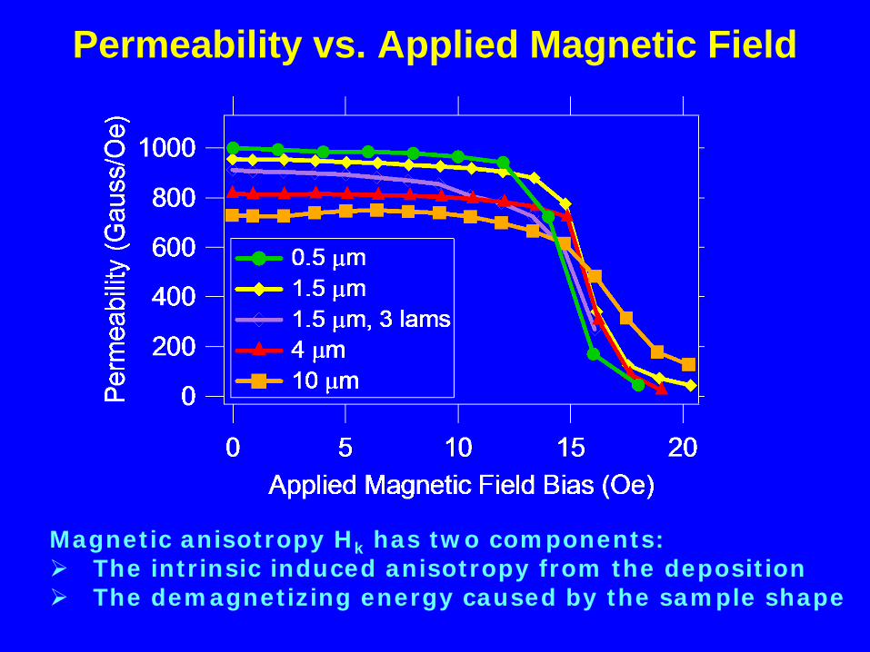
Permeability vs. Applied Magnetic Field
Magnet ic anisot ropy H k has tw o com ponents: The int r insic induced anisot ropy from the deposit io n The dem agnet iz ing energy caused by the sam ple shape

Complex Permeability Model
oiµωµρδ 2
=
High resistivity materials are needed to reduce the eddy currents and
increase the skin depth.
δδµµ
2
)1(tanh
)1(
2 dj
dji
++
=
δ = skin depthρ = resist iv ity of magnet ic filmω = frequencyµi = relat ive dc permeabilityd = film thickness
CoZrTa ρ = 1 0 0 µΩ- cm

Real Com ponent I m aginary Com ponent
Permeability Spectra of CoZrTa

Real Com ponent I m aginary Com ponent
Permeability Spectra of CoZrTa

Inductance Modeling of Wire with Magnetic Material
Maximum Increase in Inductance
Magnetic Material
Magnetic Material
Wire
2 layers magnetic film ≤ µr ×1 layer magnetic film ≤ 2 ×
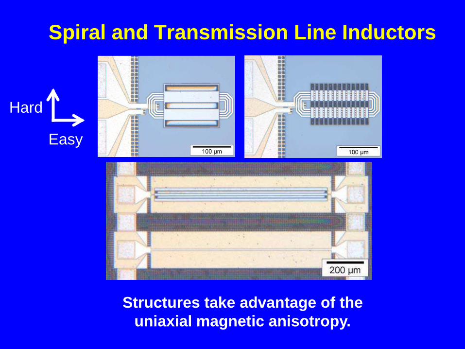
Spiral and Transmission Line Inductors
Structures take advantage of the uniaxial magnetic anisotropy.
Hard
Easy

Cross- Sectional Image of Inductor in 130 nm 6 -level Metal CMOS Process
CoZrTa
CoZrTa
Inductor Metal
Cu (M6)
Cu (M4)
Cu (M2)Cu (M1)
Cu (M3)
Cu (M5)
HardAxis Magnetic
Via
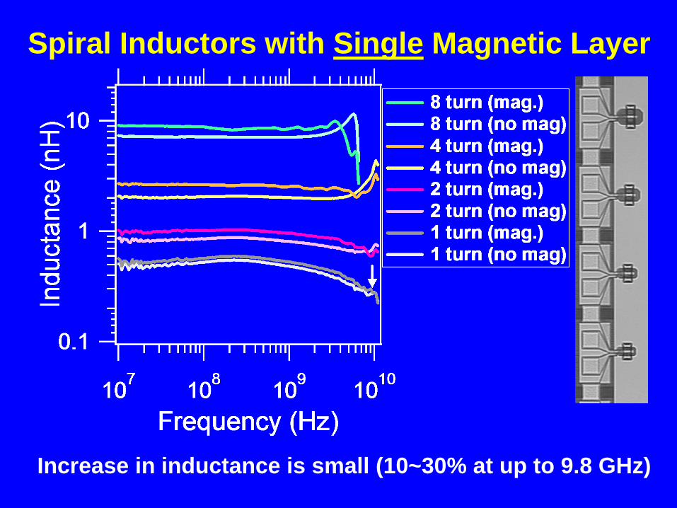
Spiral Inductors with Single Magnetic Layer
Increase in inductance is small (10~30% at up to 9.8 GHz)

Inductance increases by 9 ×
Spiral Inductors with Two Magnetic Layers

Magnetic Flux Density At 1GHz
Unlam inatedCobalt a lloy
Lam inatedCobalt a lloy
Skin-depth effect lim its penet rat ion of B- field.Larger skin depth results in lower losses.
B- field (T)
4.0
3.63.22.82.42.01.61.20.80.40.0
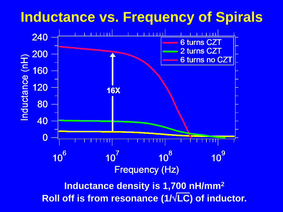
Inductance vs. Frequency of Spirals
Inductance density is 1,700 nH/mm 2
Roll off is from resonance (1/ √LC) of inductor.

Spiral and Stripe InductorsUsing 5um thick Copper
Structures take advantage of the uniaxial magnetic anisotropy.
Hard
Easy
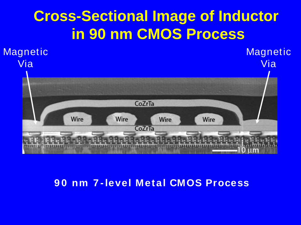
Cross -Sectional Image of Inductorin 90 nm CMOS Process
9 0 nm 7 - level Meta l CMOS Process
Magnet icVia
Magnet icVia

Cross- Sectional Image of Inductor
HardAxis

Inductance increases by up to over 30 ×
Stripe Inductors With Thick Copper

Inductance Modeling of Rectangular Line
≈
w
ltL m
r 20µµl = line lengthw = line widthtm = m agnet ic film thicknessµr = relat ive dc perm eability
1/l·Lsheet
1/Lshunt
1/L
Wtot
w
Eqn. from V. Korenivski and R. B. van Dover, JAP, v. 82 (10) , 1997

Magnetic Via Widths
I nductance increases w ith via w idth, but the change becom es dim inishingly sm all.

Sheet and Shunt Inductances
Sheet inductance is independent of the magnetic via width.Shunt inductance increases with increasing via width.

Current Density At 100 MHz
Unlam inatedCobalt a lloy
Lam inatedCobalt a lloy
Eddy currents are reduced by lam inat ions.
J( A/ m 2 )
1E+ 9
9E+ 88E+ 87E+ 96E+ 85E+ 84E+ 93E+ 82E+ 81E+ 80E+ 0

Analytical Modeling of Q -Factor
Thinner films give higher Q -factors, but lower inductance.

Analytical Modeling of Q -Factor
Laminations increase the Q -factor.

Quality Factor of Inductors With Laminated Magnetic Films
Peak quality factor is increased,But quality factor at lower frequencies decreased.

Summary• DC Voltage Converters
– High -frequency buck converters– High inductance density needed– Low DC resistance important
• Magnetic materials– Complex permeability (real and imaginary) – Low hysteretic losses– CMOS compatibility (thermal, process compatibility)
• Inductors with magnetic material– Single films increase inductance by ≤30% up to 9.8 GHz– Magnetic vias – Sheet inductance vs. shunt inductance– 2 magnetic films increase inductance
• Over 30× compared to air -core• 200 nH inductors possible (1,700 nH/mm 2)

For More Information
• IEEE Trans. Magnetics, 45, pp. 4760, 2009.
• Journal of Applied Physics, 103, pp. 07E927, Apr. 1, 2008.
• IEEE Trans. Magnetics, 43, pp. 2615, 2007.
• IEEE PESC 2004 and IEEE VLSI Symp. 2004.
• APEC, Paper #SP1.4.2, p. 75, 2010.
• Intl. Electron Devices Meeting (IEDM), pp. 221-224, 2006.
• IEEE Intl. Interconnect Technology Conference, pp.101–103, 2001.
