intel® max® 10 power management user guide · 1. intel® max® 10 power management overview intel...
TRANSCRIPT
Intel® MAX® 10 Power ManagementUser Guide
Updated for Intel® Quartus® Prime Design Suite: 18.0
SubscribeSend Feedback
UG-M10PWR | 2018.07.04Latest document on the web: PDF | HTML
Contents
1. Intel® MAX® 10 Power Management Overview.............................................................. 3
2. Intel MAX 10 Power Management Features and Architecture..........................................42.1. Power Supply Device Options.................................................................................. 4
2.1.1. Single-Supply Device................................................................................. 42.1.2. Dual-Supply Device....................................................................................42.1.3. Comparison of the Intel MAX 10 Power Supply Device Options......................... 52.1.4. Power Supply Design..................................................................................6
2.2. Power-On Reset Circuitry........................................................................................72.2.1. Power Supplies Monitored and Not Monitored by the POR Circuitry................... 82.2.2. Instant-On Support....................................................................................9
2.3. Power Management Controller Scheme..................................................................... 92.3.1. Power Management Controller Architecture................................................... 9
2.4. Hot Socketing......................................................................................................112.4.1. Hot-Socketing Specifications......................................................................122.4.2. Hot-Socketing Feature Implementation....................................................... 12
3. Power Management Controller Reference Design..........................................................143.1. Clock Control Block.............................................................................................. 153.2. I/O Buffer...........................................................................................................153.3. Internal Oscillator................................................................................................ 153.4. Power Management Controller............................................................................... 15
3.4.1. Entering State......................................................................................... 163.4.2. Sleep State............................................................................................. 163.4.3. Exiting State........................................................................................... 163.4.4. Awake State............................................................................................16
3.5. Entering or Exiting Sleep Mode.............................................................................. 173.5.1. Entering Sleep Mode.................................................................................173.5.2. Exiting Sleep Mode...................................................................................183.5.3. Timing Parameters................................................................................... 18
3.6. Hardware Implementation and Current Measurement............................................... 19
4. Intel MAX 10 Power Management User Guide Archives.................................................21
5. Document Revision History for the Intel MAX 10 Power Management User Guide.........22
Contents
Intel® MAX® 10 Power Management User Guide2
1. Intel® MAX® 10 Power Management OverviewIntel® MAX® 10 devices offer the following power supply device options:
• Single-supply device—requires 1 external power supply of 3.0 V or 3.3 V whileoffering maximum convenience and board simplicity.
• Dual-supply device—requires 2 external power supplies of 1.2 V and 2.5 V whileoffering the most features, highest performance, and when coupled with high-efficiency Enpirion® Power Solutions, the lowest power solution.
Related Information
• Intel MAX 10 Power Management Features and Architecture on page 4Provides information about power management features and architecture.
• Intel MAX 10 Power Management User Guide Archives on page 21Provides a list of user guides for previous versions.
UG-M10PWR | 2018.07.04
Intel Corporation. All rights reserved. Intel, the Intel logo, Altera, Arria, Cyclone, Enpirion, MAX, Nios, Quartusand Stratix words and logos are trademarks of Intel Corporation or its subsidiaries in the U.S. and/or othercountries. Intel warrants performance of its FPGA and semiconductor products to current specifications inaccordance with Intel's standard warranty, but reserves the right to make changes to any products and servicesat any time without notice. Intel assumes no responsibility or liability arising out of the application or use of anyinformation, product, or service described herein except as expressly agreed to in writing by Intel. Intelcustomers are advised to obtain the latest version of device specifications before relying on any publishedinformation and before placing orders for products or services.*Other names and brands may be claimed as the property of others.
ISO9001:2008Registered
2. Intel MAX 10 Power Management Features andArchitecture
Intel MAX 10 power optimization features are as follows:
• Single-supply or dual-supply device options
• Power-on reset (POR) circuitry
• Power management controller scheme
• Hot socketing
2.1. Power Supply Device Options
2.1.1. Single-Supply Device
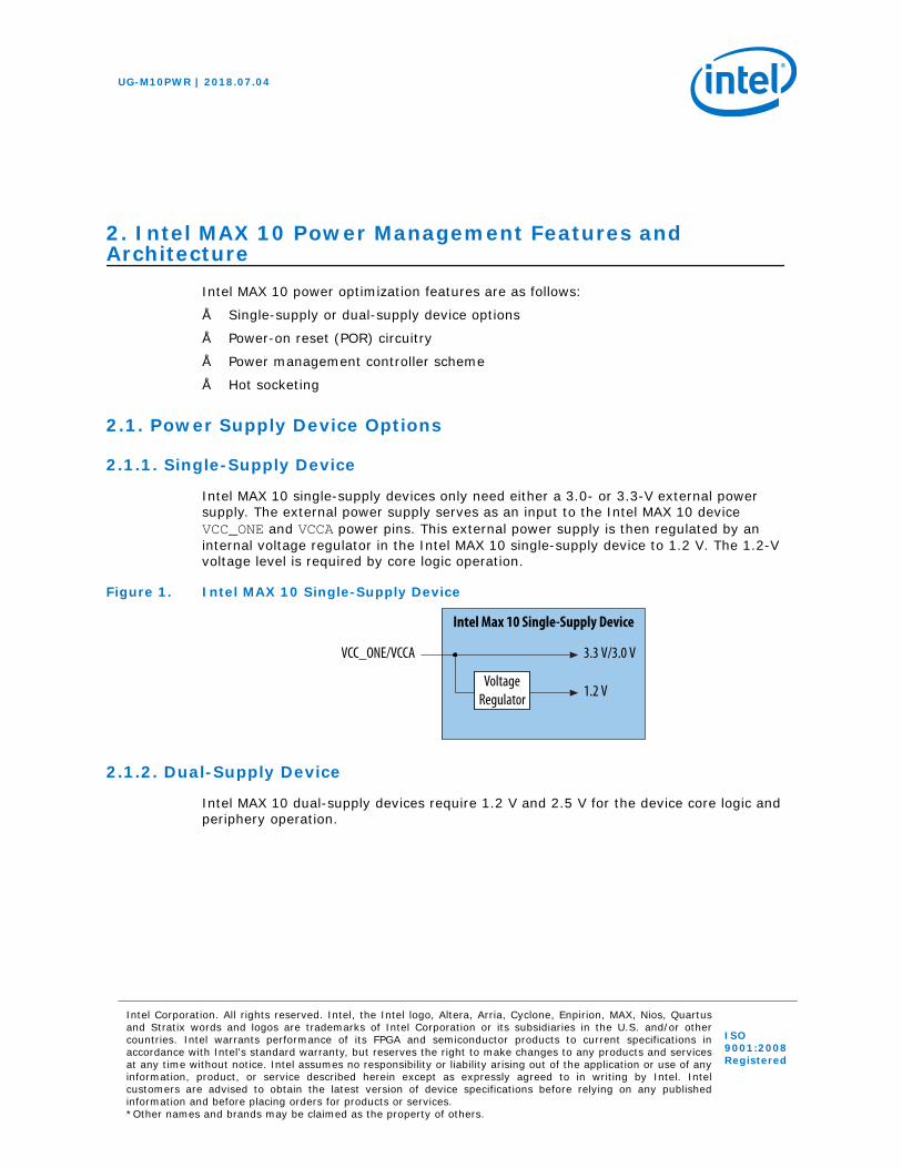
Intel MAX 10 single-supply devices only need either a 3.0- or 3.3-V external powersupply. The external power supply serves as an input to the Intel MAX 10 deviceVCC_ONE and VCCA power pins. This external power supply is then regulated by aninternal voltage regulator in the Intel MAX 10 single-supply device to 1.2 V. The 1.2-Vvoltage level is required by core logic operation.
Figure 1. Intel MAX 10 Single-Supply Device
VCC_ONE/VCCA
VoltageRegulator
3.3 V/3.0 V
1.2 V
Intel Max 10 Single-Supply Device
2.1.2. Dual-Supply Device
Intel MAX 10 dual-supply devices require 1.2 V and 2.5 V for the device core logic andperiphery operation.
UG-M10PWR | 2018.07.04
Intel Corporation. All rights reserved. Intel, the Intel logo, Altera, Arria, Cyclone, Enpirion, MAX, Nios, Quartusand Stratix words and logos are trademarks of Intel Corporation or its subsidiaries in the U.S. and/or othercountries. Intel warrants performance of its FPGA and semiconductor products to current specifications inaccordance with Intel's standard warranty, but reserves the right to make changes to any products and servicesat any time without notice. Intel assumes no responsibility or liability arising out of the application or use of anyinformation, product, or service described herein except as expressly agreed to in writing by Intel. Intelcustomers are advised to obtain the latest version of device specifications before relying on any publishedinformation and before placing orders for products or services.*Other names and brands may be claimed as the property of others.
ISO9001:2008Registered
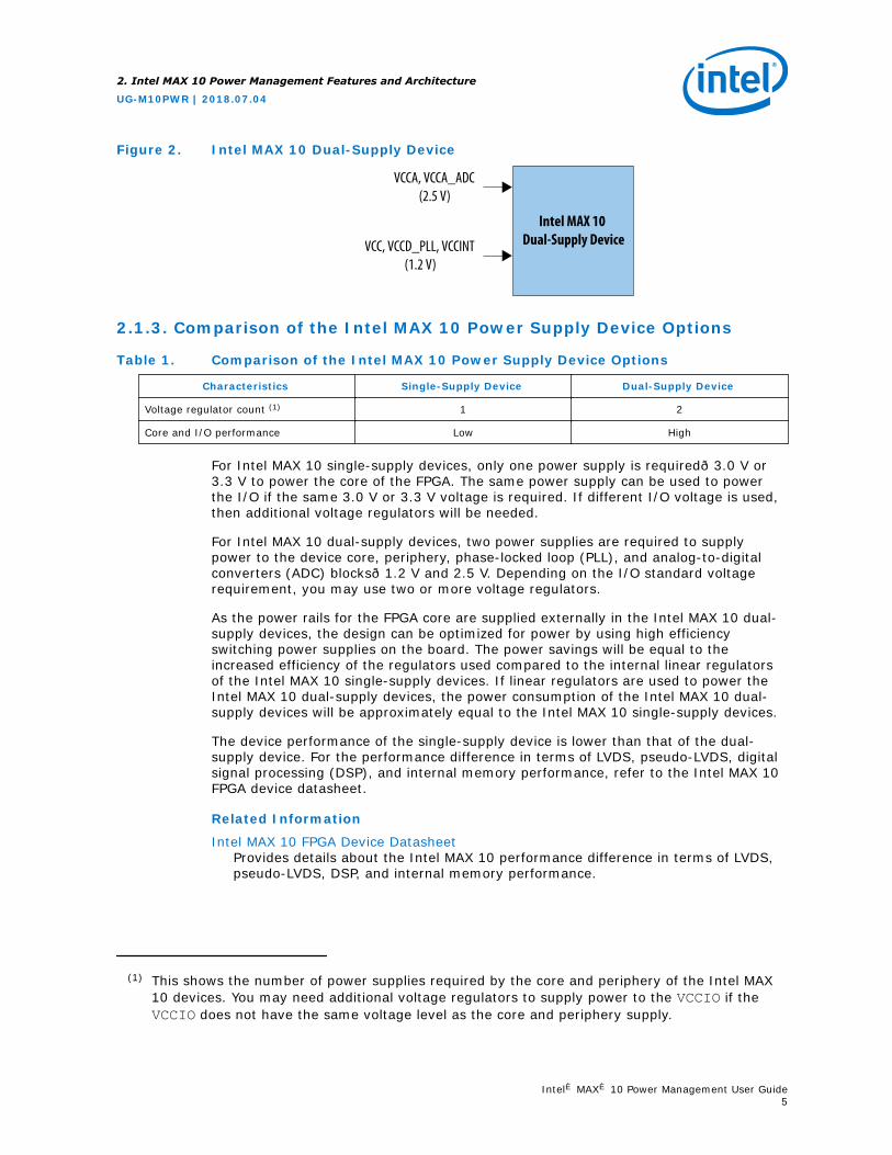
Figure 2. Intel MAX 10 Dual-Supply Device
Intel MAX 10 Dual-Supply DeviceVCC, VCCD_PLL, VCCINT
(1.2 V)
VCCA, VCCA_ADC(2.5 V)
2.1.3. Comparison of the Intel MAX 10 Power Supply Device Options
Table 1. Comparison of the Intel MAX 10 Power Supply Device Options
Characteristics Single-Supply Device Dual-Supply Device
Voltage regulator count (1) 1 2
Core and I/O performance Low High
For Intel MAX 10 single-supply devices, only one power supply is required—3.0 V or3.3 V to power the core of the FPGA. The same power supply can be used to powerthe I/O if the same 3.0 V or 3.3 V voltage is required. If different I/O voltage is used,then additional voltage regulators will be needed.
For Intel MAX 10 dual-supply devices, two power supplies are required to supplypower to the device core, periphery, phase-locked loop (PLL), and analog-to-digitalconverters (ADC) blocks—1.2 V and 2.5 V. Depending on the I/O standard voltagerequirement, you may use two or more voltage regulators.
As the power rails for the FPGA core are supplied externally in the Intel MAX 10 dual-supply devices, the design can be optimized for power by using high efficiencyswitching power supplies on the board. The power savings will be equal to theincreased efficiency of the regulators used compared to the internal linear regulatorsof the Intel MAX 10 single-supply devices. If linear regulators are used to power theIntel MAX 10 dual-supply devices, the power consumption of the Intel MAX 10 dual-supply devices will be approximately equal to the Intel MAX 10 single-supply devices.
The device performance of the single-supply device is lower than that of the dual-supply device. For the performance difference in terms of LVDS, pseudo-LVDS, digitalsignal processing (DSP), and internal memory performance, refer to the Intel MAX 10FPGA device datasheet.
Related Information
Intel MAX 10 FPGA Device DatasheetProvides details about the Intel MAX 10 performance difference in terms of LVDS,pseudo-LVDS, DSP, and internal memory performance.
(1) This shows the number of power supplies required by the core and periphery of the Intel MAX10 devices. You may need additional voltage regulators to supply power to the VCCIO if theVCCIO does not have the same voltage level as the core and periphery supply.
2. Intel MAX 10 Power Management Features and Architecture
UG-M10PWR | 2018.07.04
Intel® MAX® 10 Power Management User Guide5
2.1.4. Power Supply Design
Designing a power tree for a Intel MAX 10 single- or dual-supply device will varydepending on the static and dynamic power, as well as I/O and other featureutilization, for each specific use case.
The Intel Enpirion portfolio of power management solutions, combined withcomprehensive design tools, enable optimized Intel MAX 10 device power supplydesign. The Enpirion portfolio includes power management solutions that arecompatible with all Intel MAX 10 variants.
The Intel MAX 10 FPGA Device Family Pin Connection Guidelines provides a moredetailed recommendation about how to group inputs to power a Intel MAX 10 device.The Early Power Estimators (EPE) tool for Intel MAX 10 devices provides input railpower requirements and specific device recommendations based on each specific IntelMAX 10 use case.
Individual input rail voltage and current requirements are summarized on the Reporttab while input rail groupings and specific power supply recommendations can befound on the Main and Enpirion tabs, respectively.
Warning: Intel MAX 10 single-supply devices have maximum power consumption of VCC_ONE, aslisted in the following table. Running a design that goes beyond the maximum powerconsumption of VCC_ONE of the Intel MAX 10 single-supply device may cause functionalissue on the device. Therefore, ensure that your device does not exceed the maximumpower consumption of VCC_ONE when you analyze the power consumption of yourdesign using the EPE spreadsheet.
Table 2. Maximum Power Consumption of VCC_ONE for Intel MAX 10 Single-SupplyDevices
Device Maximum Power Consumption (W)
10M02S 0.778
10M04S 1.362
10M08S 1.362
10M16S 2.270
10M25S 2.943
10M40S 5.267
10M50S 5.267
Related Information
• Enpirion Power Management SolutionsProvides more information about Intel's Power Management IC and Powersolutions designed for powering FPGAs.
• Intel MAX 10 FPGA Device Family Pin Connection GuidelinesProvides a more detailed recommendation about how to group inputs in orderto power an Intel MAX 10 device.
• Early Power Estimators (EPE) and Power Analyzer
2. Intel MAX 10 Power Management Features and Architecture
UG-M10PWR | 2018.07.04
Intel® MAX® 10 Power Management User Guide6
2.1.4.1. Transient Current
You may observe a transient current at the VCCIO power supply when powering up theIntel MAX 10 devices. The transient current of VCCIO applies to all VCCIO voltage levelssupported by the Intel MAX 10 device.
Table 3. Maximum VCCIO Power Supply Transient Current for Intel MAX 10 Devices
Device Maximum Power Supply Transient Current (mA) Duration (s)
10M02 220 25% of the ramp time
10M04 290
10M08 300
10M16 430
10M25 510
10M40 670
10M50 680
Note: The value of the transient current is based on the zero decoupling capacitance on thecharacterization board. The observed value will be less than the published value afteradding the decoupling capacitance on your design board. Intel recommends using asoft start regulator that is able to reduce the transient current when the device ispowered.
2.2. Power-On Reset Circuitry
The POR circuitry keeps the Intel MAX 10 device in the reset state until all powersupplies reach the recommended operating range during device power up. Theindividual power supply must reach the recommended operating range within themaximum power supply ramp time, tRAMP.
If the ramp time, tRAMP, is not met, the Intel MAX 10 device I/O pins and programmingregisters remain tri-stated, during which device configuration could fail.
The Intel MAX 10 device POR circuit monitors the following power rails during powerup regardless of the power supply device options:
• VCC or regulated VCC_ONE
• VCCIO of banks 1B and 8 (2)
• VCCA
The POR circuitry also ensures VCCIO level of I/O banks 1B and 8(2) that containconfiguration pins reach an acceptable level before configuration is triggered.
(2) VCCIO of banks 1 and 8 for the 10M02 device.
2. Intel MAX 10 Power Management Features and Architecture
UG-M10PWR | 2018.07.04
Intel® MAX® 10 Power Management User Guide7
2.2.1. Power Supplies Monitored and Not Monitored by the POR Circuitry
Table 4. Power Supplies Monitored and Not Monitored by the POR Circuitry
Power Supply Device Options Power Supplies Monitored Power Supplies Not Monitored
Single-supply device • Regulated VCC_ONE
• VCCA
• VCCIO (3)
—
Dual-supply device • VCC
• VCCA
• VCCIO(3)
• VCCD_PLL
• VCCA_ADC
• VCCINT
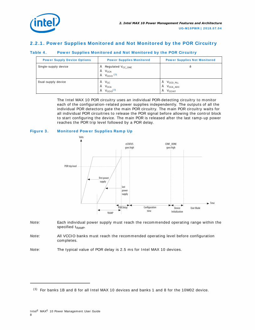
The Intel MAX 10 POR circuitry uses an individual POR-detecting circuitry to monitoreach of the configuration-related power supplies independently. The outputs of all theindividual POR detectors gate the main POR circuitry. The main POR circuitry waits forall individual POR circuitries to release the POR signal before allowing the control blockto start configuring the device. The main POR is released after the last ramp-up powerreaches the POR trip level followed by a POR delay.
Figure 3. Monitored Power Supplies Ramp Up
Time
POR trip level
Volts
POR Delay Configuration time
DeviceInitialization
User Mode
tRAMP
first power supply
last powersupply
nSTATUSgoes high
CONF_DONEgoes high
Note: Each individual power supply must reach the recommended operating range within thespecified tRAMP.
Note: All VCCIO banks must reach the recommended operating level before configurationcompletes.
Note: The typical value of POR delay is 2.5 ms for Intel MAX 10 devices.
(3) For banks 1B and 8 for all Intel MAX 10 devices and banks 1 and 8 for the 10M02 device.
2. Intel MAX 10 Power Management Features and Architecture
UG-M10PWR | 2018.07.04
Intel® MAX® 10 Power Management User Guide8
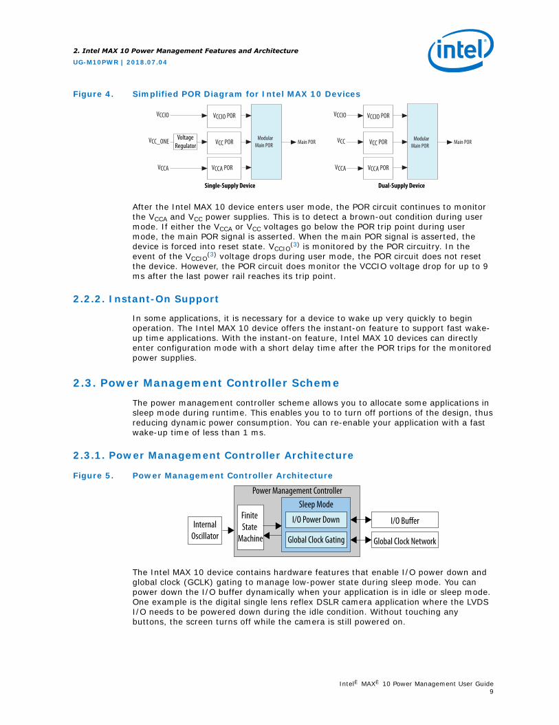
Figure 4. Simplified POR Diagram for Intel MAX 10 Devices
VCCIO
ModularMain POR
Main POR
VCCA
VCCIO POR
VCC VCC POR
VCCA POR
VCCIO
ModularMain POR Main POR
VCCA
VCCIO POR
VCC_ONE VCC POR
VCCA POR
VoltageRegulator
Single-Supply Device Dual-Supply Device
After the Intel MAX 10 device enters user mode, the POR circuit continues to monitorthe VCCA and VCC power supplies. This is to detect a brown-out condition during usermode. If either the VCCA or VCC voltages go below the POR trip point during usermode, the main POR signal is asserted. When the main POR signal is asserted, thedevice is forced into reset state. VCCIO
(3) is monitored by the POR circuitry. In theevent of the VCCIO
(3) voltage drops during user mode, the POR circuit does not resetthe device. However, the POR circuit does monitor the VCCIO voltage drop for up to 9ms after the last power rail reaches its trip point.
2.2.2. Instant-On Support
In some applications, it is necessary for a device to wake up very quickly to beginoperation. The Intel MAX 10 device offers the instant-on feature to support fast wake-up time applications. With the instant-on feature, Intel MAX 10 devices can directlyenter configuration mode with a short delay time after the POR trips for the monitoredpower supplies.
2.3. Power Management Controller Scheme
The power management controller scheme allows you to allocate some applications insleep mode during runtime. This enables you to to turn off portions of the design, thusreducing dynamic power consumption. You can re-enable your application with a fastwake-up time of less than 1 ms.
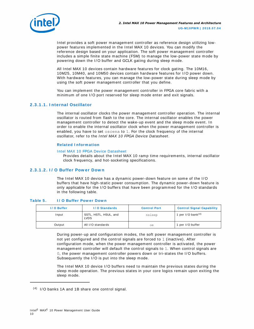
2.3.1. Power Management Controller Architecture
Figure 5. Power Management Controller Architecture
I/O Power Down
Global Clock Gating
Sleep ModeFinite State
MachineInternal
Oscillator
Power Management Controller
I/O Buffer
Global Clock Network
The Intel MAX 10 device contains hardware features that enable I/O power down andglobal clock (GCLK) gating to manage low-power state during sleep mode. You canpower down the I/O buffer dynamically when your application is in idle or sleep mode.One example is the digital single lens reflex DSLR camera application where the LVDSI/O needs to be powered down during the idle condition. Without touching anybuttons, the screen turns off while the camera is still powered on.
2. Intel MAX 10 Power Management Features and Architecture
UG-M10PWR | 2018.07.04
Intel® MAX® 10 Power Management User Guide9
Intel provides a soft power management controller as reference design utilizing low-power features implemented in the Intel MAX 10 devices. You can modify thereference design based on your application. The soft power management controllerincludes a simple finite state machine (FSM) to manage the low-power state mode bypowering down the I/O buffer and GCLK gating during sleep mode.
All Intel MAX 10 devices contain hardware features for clock gating. The 10M16,10M25, 10M40, and 10M50 devices contain hardware features for I/O power down.With hardware features, you can manage the low-power state during sleep mode byusing the soft power management controller that you define.
You can implement the power management controller in FPGA core fabric with aminimum of one I/O port reserved for sleep mode enter and exit signals.
2.3.1.1. Internal Oscillator
The internal oscillator clocks the power management controller operation. The internaloscillator is routed from flash to the core. The internal oscillator enables the powermanagement controller to detect the wake-up event and the sleep mode event. Inorder to enable the internal oscillator clock when the power management controller isenabled, you have to set oscena to 1. For the clock frequency of the internaloscillator, refer to the Intel MAX 10 FPGA Device Datasheet.
Related Information
Intel MAX 10 FPGA Device DatasheetProvides details about the Intel MAX 10 ramp time requirements, internal oscillatorclock frequency, and hot-socketing specifications.
2.3.1.2. I/O Buffer Power Down
The Intel MAX 10 device has a dynamic power-down feature on some of the I/Obuffers that have high-static power consumption. The dynamic power-down feature isonly applicable for the I/O buffers that have been programmed for the I/O standardsin the following table.
Table 5. I/O Buffer Power Down
I/O Buffer I/O Standards Control Port Control Signal Capability
Input SSTL, HSTL, HSUL, andLVDS
nsleep 1 per I/O bank(4)
Output All I/O standards oe 1 per I/O buffer
During power-up and configuration modes, the soft power management controller isnot yet configured and the control signals are forced to 1 (inactive). Afterconfiguration mode, when the power management controller is activated, the powermanagement controller will default the control signals to 1. When control signals are0, the power management controller powers down or tri-states the I/O buffers.Subsequently the I/O is put into the sleep mode.
The Intel MAX 10 device I/O buffers need to maintain the previous states during thesleep mode operation. The previous states in your core logics remain upon exiting thesleep mode.
(4) I/O banks 1A and 1B share one control signal.
2. Intel MAX 10 Power Management Features and Architecture
UG-M10PWR | 2018.07.04
Intel® MAX® 10 Power Management User Guide10
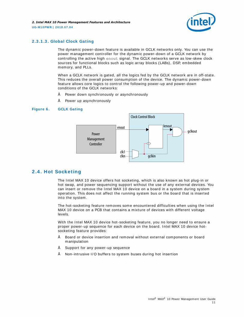
2.3.1.3. Global Clock Gating
The dynamic power-down feature is available in GCLK networks only. You can use thepower management controller for the dynamic power-down of a GCLK network bycontrolling the active high enout signal. The GCLK networks serve as low-skew clocksources for functional blocks such as logic array blocks (LABs), DSP, embeddedmemory, and PLLs.
When a GCLK network is gated, all the logics fed by the GCLK network are in off-state.This reduces the overall power consumption of the device. The dynamic power-downfeature allows core logics to control the following power-up and power-downconditions of the GCLK networks:
• Power down synchronously or asynchronously
• Power up asynchronously
Figure 6. GCLK Gating
Power Management
Controller
enout
clk1clkn gclkin
lenoutgclkout
Clock Control Block
2.4. Hot Socketing
The Intel MAX 10 device offers hot socketing, which is also known as hot plug-in orhot swap, and power sequencing support without the use of any external devices. Youcan insert or remove the Intel MAX 10 device on a board in a system during systemoperation. This does not affect the running system bus or the board that is insertedinto the system.
The hot-socketing feature removes some encountered difficulties when using the IntelMAX 10 device on a PCB that contains a mixture of devices with different voltagelevels.
With the Intel MAX 10 device hot-socketing feature, you no longer need to ensure aproper power-up sequence for each device on the board. Intel MAX 10 device hot-socketing feature provides:
• Board or device insertion and removal without external components or boardmanipulation
• Support for any power-up sequence
• Non-intrusive I/O buffers to system buses during hot insertion
2. Intel MAX 10 Power Management Features and Architecture
UG-M10PWR | 2018.07.04
Intel® MAX® 10 Power Management User Guide11
2.4.1. Hot-Socketing Specifications
The Intel MAX 10 device is a hot-socketing compliant device that does not need anyexternal components or special design requirements. Hot-socketing support in theIntel MAX 10 device has the following advantages:
• You can drive the devices before power up without damaging the device.
• I/O pins remain tri-stated during power up. The device does not drive out beforeor during power up, therefore not affecting other buses in operation.
2.4.1.1. Drive Intel MAX 10 Devices Before Power Up
Before or during power up or power down, you can drive signals into I/O pins,dedicated input pins, and dedicated clock pins without damaging the Intel MAX 10devices.
The Intel MAX 10 device supports any power-up or power-down sequence to simplifysystem-level design.
2.4.1.2. I/O Pins Remain Tri-stated During Power up
The output buffers of the Intel MAX 10 device are turned off during system power upor power down. The Intel MAX 10 device family does not drive out until the device isconfigured and working in recommended operating conditions. The I/O pins are tri-stated during power up or power down.
A possible concern for semiconductor devices in general regarding hot-socketing is thepotential for latch up. Latch up can occur when electrical subsystems are hot-socketedinto an active system. During hot-socketing, the signal pins may be connected anddriven by the active system. This occurs before the power supply can provide currentto the VCC of the device and ground planes. This condition can lead to latch up andcause a low-impedance path from VCC to ground in the device. As a result, the deviceextends a large amount of current, possibly causing electrical damage.
The design of the I/O buffers and hot-socketing circuitry ensures that the Intel MAX10 device family is immune to latch up during hot-socketing.
Related Information
Intel MAX 10 FPGA Device DatasheetProvides details about the Intel MAX 10 ramp time requirements, internal oscillatorclock frequency, and hot-socketing specifications.
2.4.2. Hot-Socketing Feature Implementation
The hot-socketing feature tri-states the output buffer during the power-up (VCCIO orVCC power supplies) or power-down event. The hot-socketing circuitry generates aninternal HOTSCKT signal when VCCIO or VCC is below the threshold voltage duringpower up or power down. The HOTSCKT signal cuts off the output buffer to ensure thatno DC current leaks through the pin. Each I/O pin has the circuitry shown in thefollowing figure. The hot-socketing circuit does not include CONF_DONE and nSTATUSpins to ensure that these pins are able to operate during configuration. Thus, it is anexpected behavior for these pins to drive out during power-up and power-downsequences.
2. Intel MAX 10 Power Management Features and Architecture
UG-M10PWR | 2018.07.04
Intel® MAX® 10 Power Management User Guide12
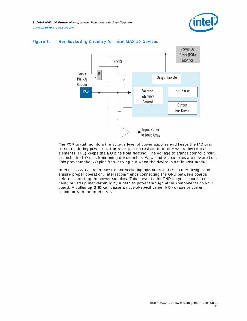
Figure 7. Hot-Socketing Circuitry for Intel MAX 10 Devices
VCCIO
PAD
R
VoltageTolerance
Control
Output Enable
Hot-Socket
OutputPre-Driver
Power-OnReset (POR)
Monitor
WeakPull-UpResistor
Input Bufferto Logic Array
The POR circuit monitors the voltage level of power supplies and keeps the I/O pinstri-stated during power up. The weak pull-up resistor in Intel MAX 10 device I/Oelements (IOE) keeps the I/O pins from floating. The voltage tolerance control circuitprotects the I/O pins from being driven before VCCIO and VCC supplies are powered up.This prevents the I/O pins from driving out when the device is not in user mode.
Intel uses GND as reference for hot-socketing operation and I/O buffer designs. Toensure proper operation, Intel recommends connecting the GND between boardsbefore connecting the power supplies. This prevents the GND on your board frombeing pulled up inadvertently by a path to power through other components on yourboard. A pulled up GND can cause an out-of-specification I/O voltage or currentcondition with the Intel FPGA.
2. Intel MAX 10 Power Management Features and Architecture
UG-M10PWR | 2018.07.04
Intel® MAX® 10 Power Management User Guide13
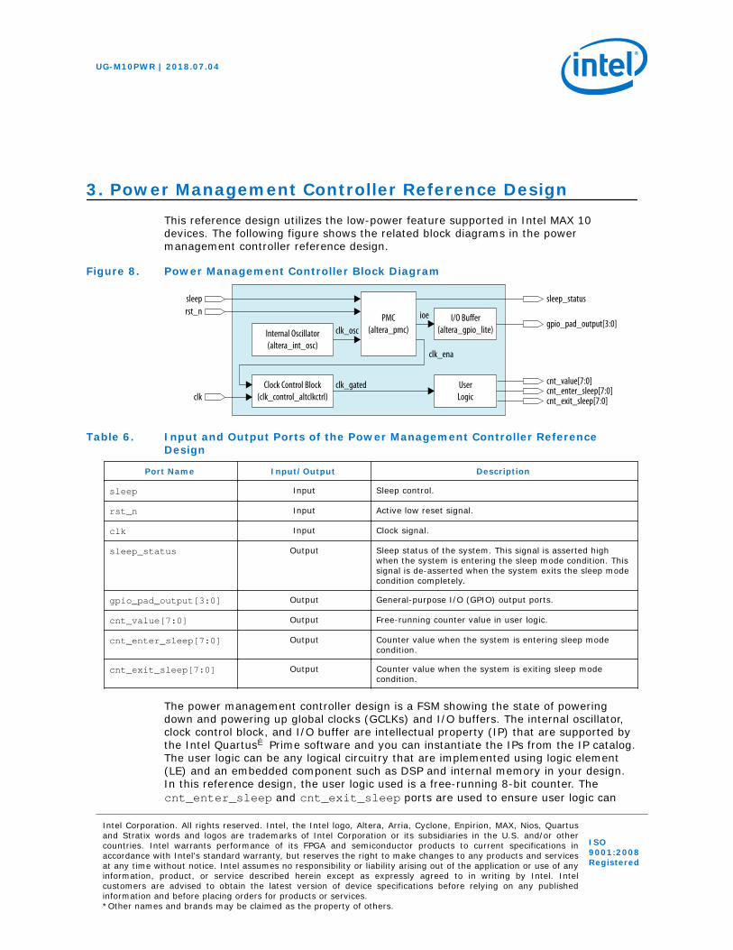
3. Power Management Controller Reference DesignThis reference design utilizes the low-power feature supported in Intel MAX 10devices. The following figure shows the related block diagrams in the powermanagement controller reference design.
Figure 8. Power Management Controller Block Diagram
PMC(altera_pmc)Internal Oscillator
(altera_int_osc)
sleeprst_n
Clock Control Block(clk_control_altclkctrl)
clk_osc
clk
I/O Buffer(altera_gpio_lite)
UserLogic
sleep_status
gpio_pad_output[3:0]
cnt_enter_sleep[7:0]cnt_value[7:0]
cnt_exit_sleep[7:0]
clk_gated
ioe
clk_ena
Table 6. Input and Output Ports of the Power Management Controller ReferenceDesign
Port Name Input/Output Description
sleep Input Sleep control.
rst_n Input Active low reset signal.
clk Input Clock signal.
sleep_status Output Sleep status of the system. This signal is asserted highwhen the system is entering the sleep mode condition. Thissignal is de-asserted when the system exits the sleep modecondition completely.
gpio_pad_output[3:0] Output General-purpose I/O (GPIO) output ports.
cnt_value[7:0] Output Free-running counter value in user logic.
cnt_enter_sleep[7:0] Output Counter value when the system is entering sleep modecondition.
cnt_exit_sleep[7:0] Output Counter value when the system is exiting sleep modecondition.
The power management controller design is a FSM showing the state of poweringdown and powering up global clocks (GCLKs) and I/O buffers. The internal oscillator,clock control block, and I/O buffer are intellectual property (IP) that are supported bythe Intel Quartus® Prime software and you can instantiate the IPs from the IP catalog.The user logic can be any logical circuitry that are implemented using logic element(LE) and an embedded component such as DSP and internal memory in your design.In this reference design, the user logic used is a free-running 8-bit counter. Thecnt_enter_sleep and cnt_exit_sleep ports are used to ensure user logic can
UG-M10PWR | 2018.07.04
Intel Corporation. All rights reserved. Intel, the Intel logo, Altera, Arria, Cyclone, Enpirion, MAX, Nios, Quartusand Stratix words and logos are trademarks of Intel Corporation or its subsidiaries in the U.S. and/or othercountries. Intel warrants performance of its FPGA and semiconductor products to current specifications inaccordance with Intel's standard warranty, but reserves the right to make changes to any products and servicesat any time without notice. Intel assumes no responsibility or liability arising out of the application or use of anyinformation, product, or service described herein except as expressly agreed to in writing by Intel. Intelcustomers are advised to obtain the latest version of device specifications before relying on any publishedinformation and before placing orders for products or services.*Other names and brands may be claimed as the property of others.
ISO9001:2008Registered
enter and exit sleep mode without data corruption. It is expected for thatcnt_enter_sleep[7:0] and cnt_exit_sleep[7:0] are at the same value afterthe user logic enter and exit sleep mode. gpio_pad_output ports demonstrate tri-stated state of the GPIO when the system is in sleep mode.
Related Information
Power Management Controller Reference Design
3.1. Clock Control Block
The ALTCLKCTRL Intel FPGA IP core (clk_control_altclkctrl) is an IP providedin the Intel Quartus Prime software. This IP is used to control the clock system in thedevice. The GCLKs that drive through the device can be dynamically powered down bycontrolling the active high ena signal. The ena port is an input to the clock control IPblock. When this IP is instantiated, select the ena port to enable the controls ofGCLKs.
Related Information
ALTCLKCTRL Intel FPGA IP Core User Guide
3.2. I/O Buffer
The GPIO Lite Intel FPGA IP core (altera_gpio_lite) is implemented as an input,output, or bidirectional I/O buffer. You can control the power down of these I/O buffersby enabling the nsleep port of the input buffer and the oe port of the output buffer.The oe and nsleep ports are pulled low by the power management controller designto power down the I/O buffers during sleep mode. Intel recommends using a separateGPIO Lite Intel FPGA IP core when some of the I/O buffer is not required to bepowered down.
Related Information
GPIO Lite Intel FPGA IP Core References
3.3. Internal Oscillator
Internal Oscillator Intel FPGA IP core (altera_in_osc) is a free-running oscillatoronce you enable it. This oscillator runs throughout the entire power managementcontroller design.
Related Information
Internal Oscillator Intel FPGA IP Core
3.4. Power Management Controller
The power management controller implements a simple FSM to control the power-upand power-down sequences of the GCLK networks and I/O buffer.
3. Power Management Controller Reference Design
UG-M10PWR | 2018.07.04
Intel® MAX® 10 Power Management User Guide15
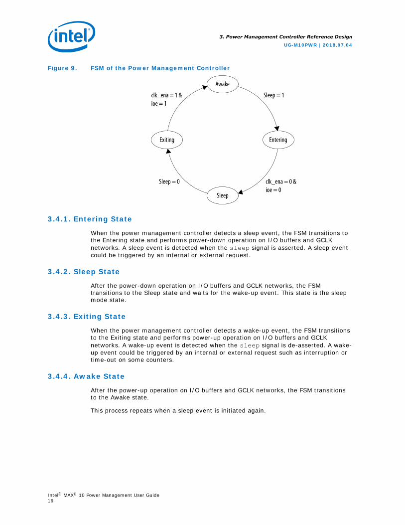
Figure 9. FSM of the Power Management Controller
Awake
Sleep
EnteringExiting
Sleep = 1clk_ena = 1 &ioe = 1
clk_ena = 0 &ioe = 0
Sleep = 0
3.4.1. Entering State
When the power management controller detects a sleep event, the FSM transitions tothe Entering state and performs power-down operation on I/O buffers and GCLKnetworks. A sleep event is detected when the sleep signal is asserted. A sleep eventcould be triggered by an internal or external request.
3.4.2. Sleep State
After the power-down operation on I/O buffers and GCLK networks, the FSMtransitions to the Sleep state and waits for the wake-up event. This state is the sleepmode state.
3.4.3. Exiting State
When the power management controller detects a wake-up event, the FSM transitionsto the Exiting state and performs power-up operation on I/O buffers and GCLKnetworks. A wake-up event is detected when the sleep signal is de-asserted. A wake-up event could be triggered by an internal or external request such as interruption ortime-out on some counters.
3.4.4. Awake State
After the power-up operation on I/O buffers and GCLK networks, the FSM transitionsto the Awake state.
This process repeats when a sleep event is initiated again.
3. Power Management Controller Reference Design
UG-M10PWR | 2018.07.04
Intel® MAX® 10 Power Management User Guide16
3.5. Entering or Exiting Sleep Mode
During power-up and configuration modes, the sleep signal must be low. When thesleep signal is asserted, the device immediately enters sleep mode. Upon enteringsleep mode, the functionality of the device such as GCLK networks and I/O buffers aredynamically powered down—to minimize dynamic power dissipation. All configurationdata is retained when the device is in the sleep mode.
3.5.1. Entering Sleep Mode
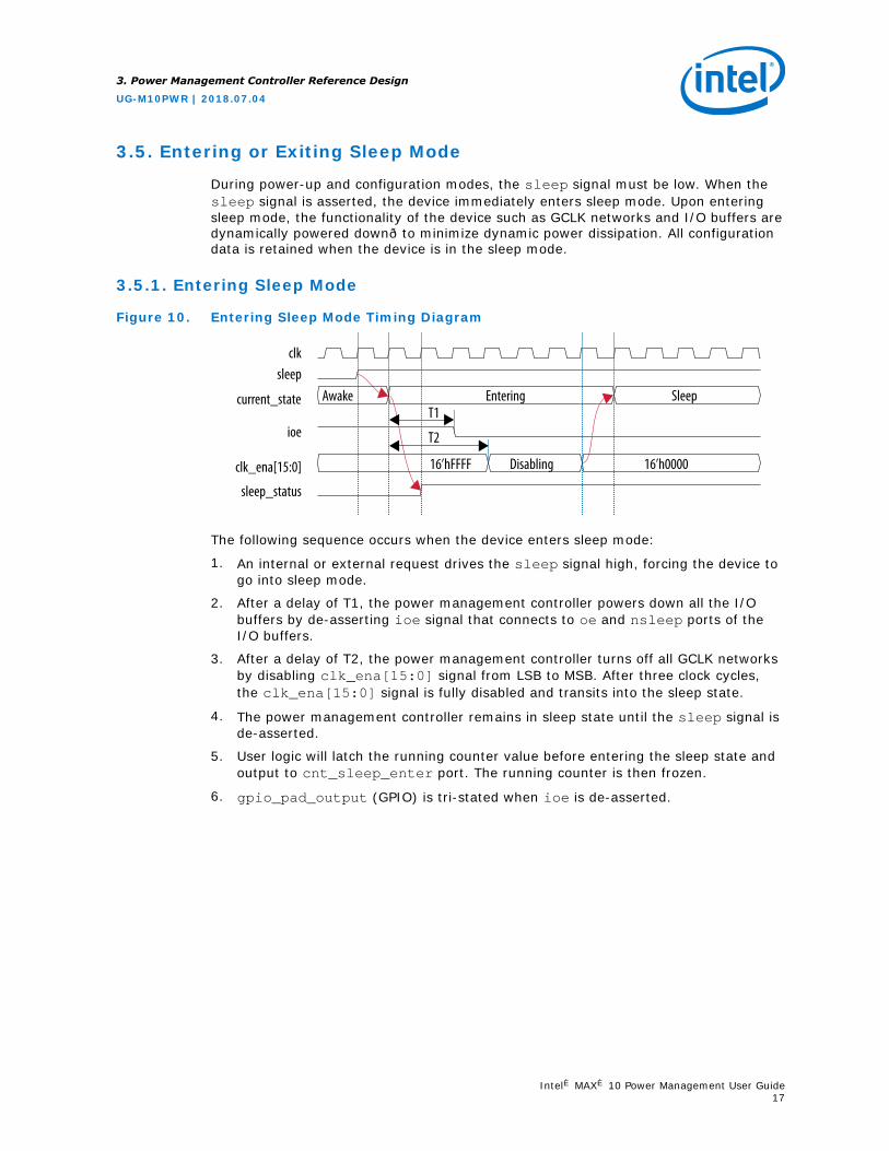
Figure 10. Entering Sleep Mode Timing Diagram
clksleep
current_state
ioe
clk_ena[15:0]
sleep_status
Awake Entering Sleep
16’hFFFF Disabling 16’h0000
T1
T2
The following sequence occurs when the device enters sleep mode:
1. An internal or external request drives the sleep signal high, forcing the device togo into sleep mode.
2. After a delay of T1, the power management controller powers down all the I/Obuffers by de-asserting ioe signal that connects to oe and nsleep ports of theI/O buffers.
3. After a delay of T2, the power management controller turns off all GCLK networksby disabling clk_ena[15:0] signal from LSB to MSB. After three clock cycles,the clk_ena[15:0] signal is fully disabled and transits into the sleep state.
4. The power management controller remains in sleep state until the sleep signal isde-asserted.
5. User logic will latch the running counter value before entering the sleep state andoutput to cnt_sleep_enter port. The running counter is then frozen.
6. gpio_pad_output (GPIO) is tri-stated when ioe is de-asserted.
3. Power Management Controller Reference Design
UG-M10PWR | 2018.07.04
Intel® MAX® 10 Power Management User Guide17
3.5.2. Exiting Sleep Mode
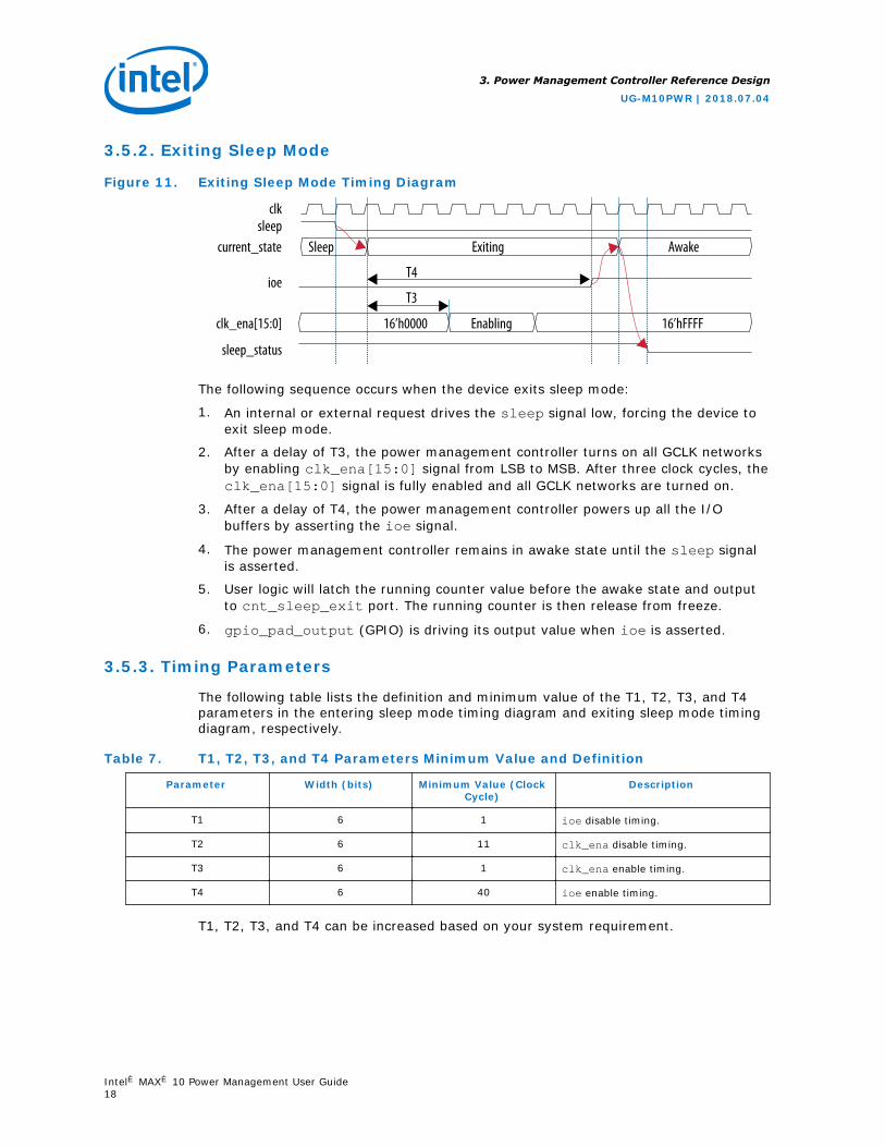
Figure 11. Exiting Sleep Mode Timing Diagram
clksleep
current_state
ioe
clk_ena[15:0]
sleep_status
Sleep Exiting Awake
16’hFFFFEnabling16’h0000
T4
T3
The following sequence occurs when the device exits sleep mode:
1. An internal or external request drives the sleep signal low, forcing the device toexit sleep mode.
2. After a delay of T3, the power management controller turns on all GCLK networksby enabling clk_ena[15:0] signal from LSB to MSB. After three clock cycles, theclk_ena[15:0] signal is fully enabled and all GCLK networks are turned on.
3. After a delay of T4, the power management controller powers up all the I/Obuffers by asserting the ioe signal.
4. The power management controller remains in awake state until the sleep signalis asserted.
5. User logic will latch the running counter value before the awake state and outputto cnt_sleep_exit port. The running counter is then release from freeze.
6. gpio_pad_output (GPIO) is driving its output value when ioe is asserted.
3.5.3. Timing Parameters
The following table lists the definition and minimum value of the T1, T2, T3, and T4parameters in the entering sleep mode timing diagram and exiting sleep mode timingdiagram, respectively.
Table 7. T1, T2, T3, and T4 Parameters Minimum Value and Definition
Parameter Width (bits) Minimum Value (ClockCycle)
Description
T1 6 1 ioe disable timing.
T2 6 11 clk_ena disable timing.
T3 6 1 clk_ena enable timing.
T4 6 40 ioe enable timing.
T1, T2, T3, and T4 can be increased based on your system requirement.
3. Power Management Controller Reference Design
UG-M10PWR | 2018.07.04
Intel® MAX® 10 Power Management User Guide18

3.6. Hardware Implementation and Current Measurement
This design is implemented using the 10M50DAF484C6 device. You can implement thisdesign using any Intel MAX 10 device. This design runs on the Intel MAX 10Development Kit Board to show current and power relative between user mode andsleep mode.
The resource utilization of this design is as follows:
• 42,000 LEs (84% of total LEs)—gray counter top module utilizes most of the LEsin the device
• 33 I/O pins (9% of total pins)—covering 3 input pins and 30 output pins
The current in this design is measured using a current monitor component (the LinearTechnologies LTC 2990). The measured current is further processed by a pre-programmed design in a MAX II device. The measured current is shown on Intel FPGApower monitor GUI when the PowerMonitor.exe is launched. You will see a currentmonitor for each of the main supplies to the Intel MAX 10 device as follows:
• 2.5V_CORE(5)
• 2.5V_VCCIO
• 1.5V_VCCIO
• 1.2V_VCC
For design demonstration purpose, the push button is used for sleep control and theLEDs are used for sleep status. Thus, these signals have been inverted on the pinlevel. To enter sleep mode, press and hold the push button USER_PB0. To release thedesign to user mode, release the push button USER_PB0. LED0 indicates the sleepstatus of the device. LED0 is turned on when the device enters sleep mode and isturned off when the device is in user mode. During sleep mode, gpio_pad_outputports connecting to LED1–LED4 are tri-stated and then turned off.
(5) This is 2.5V_VCCA.
3. Power Management Controller Reference Design
UG-M10PWR | 2018.07.04
Intel® MAX® 10 Power Management User Guide19
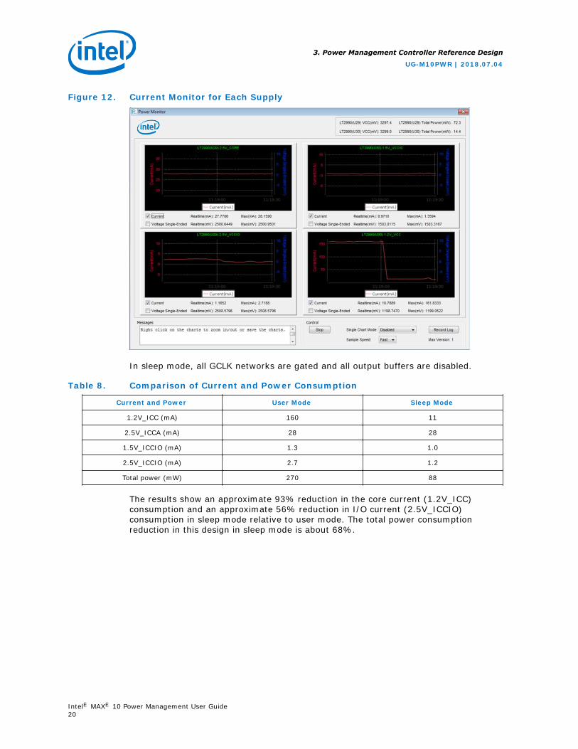
Figure 12. Current Monitor for Each Supply
In sleep mode, all GCLK networks are gated and all output buffers are disabled.
Table 8. Comparison of Current and Power Consumption
Current and Power User Mode Sleep Mode
1.2V_ICC (mA) 160 11
2.5V_ICCA (mA) 28 28
1.5V_ICCIO (mA) 1.3 1.0
2.5V_ICCIO (mA) 2.7 1.2
Total power (mW) 270 88
The results show an approximate 93% reduction in the core current (1.2V_ICC)consumption and an approximate 56% reduction in I/O current (2.5V_ICCIO)consumption in sleep mode relative to user mode. The total power consumptionreduction in this design in sleep mode is about 68%.
3. Power Management Controller Reference Design
UG-M10PWR | 2018.07.04
Intel® MAX® 10 Power Management User Guide20
4. Intel MAX 10 Power Management User Guide ArchivesIf an IP core version is not listed, the user guide for the previous IP core version applies.
IP Core Version User Guide
15.1 MAX 10 Power Management User Guide
15.0 MAX 10 Power Management User Guide
14.1 MAX 10 Power Management User Guide
UG-M10PWR | 2018.07.04
Intel Corporation. All rights reserved. Intel, the Intel logo, Altera, Arria, Cyclone, Enpirion, MAX, Nios, Quartusand Stratix words and logos are trademarks of Intel Corporation or its subsidiaries in the U.S. and/or othercountries. Intel warrants performance of its FPGA and semiconductor products to current specifications inaccordance with Intel's standard warranty, but reserves the right to make changes to any products and servicesat any time without notice. Intel assumes no responsibility or liability arising out of the application or use of anyinformation, product, or service described herein except as expressly agreed to in writing by Intel. Intelcustomers are advised to obtain the latest version of device specifications before relying on any publishedinformation and before placing orders for products or services.*Other names and brands may be claimed as the property of others.
ISO9001:2008Registered
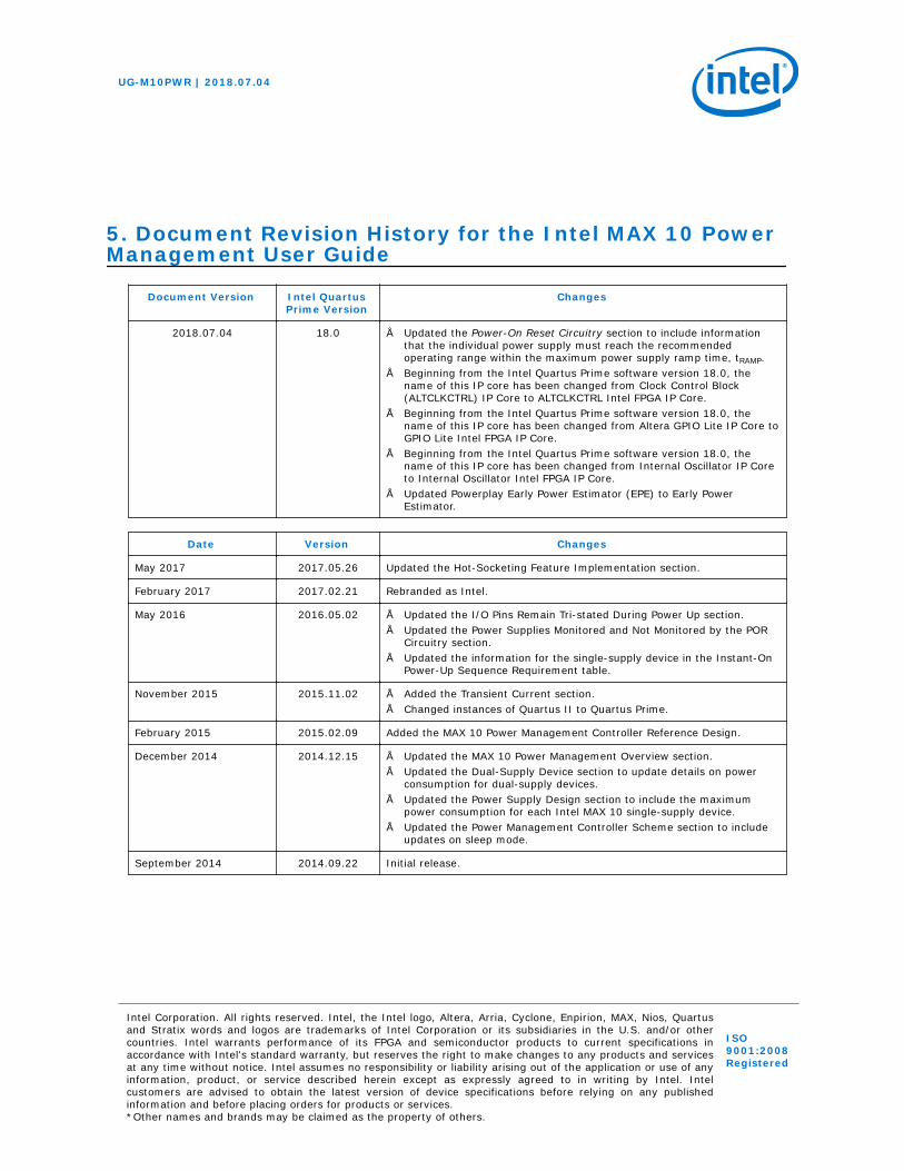
5. Document Revision History for the Intel MAX 10 PowerManagement User Guide
Document Version Intel QuartusPrime Version
Changes
2018.07.04 18.0 • Updated the Power-On Reset Circuitry section to include informationthat the individual power supply must reach the recommendedoperating range within the maximum power supply ramp time, tRAMP.
• Beginning from the Intel Quartus Prime software version 18.0, thename of this IP core has been changed from Clock Control Block(ALTCLKCTRL) IP Core to ALTCLKCTRL Intel FPGA IP Core.
• Beginning from the Intel Quartus Prime software version 18.0, thename of this IP core has been changed from Altera GPIO Lite IP Core toGPIO Lite Intel FPGA IP Core.
• Beginning from the Intel Quartus Prime software version 18.0, thename of this IP core has been changed from Internal Oscillator IP Coreto Internal Oscillator Intel FPGA IP Core.
• Updated Powerplay Early Power Estimator (EPE) to Early PowerEstimator.
Date Version Changes
May 2017 2017.05.26 Updated the Hot-Socketing Feature Implementation section.
February 2017 2017.02.21 Rebranded as Intel.
May 2016 2016.05.02 • Updated the I/O Pins Remain Tri-stated During Power Up section.• Updated the Power Supplies Monitored and Not Monitored by the POR
Circuitry section.• Updated the information for the single-supply device in the Instant-On
Power-Up Sequence Requirement table.
November 2015 2015.11.02 • Added the Transient Current section.• Changed instances of Quartus II to Quartus Prime.
February 2015 2015.02.09 Added the MAX 10 Power Management Controller Reference Design.
December 2014 2014.12.15 • Updated the MAX 10 Power Management Overview section.• Updated the Dual-Supply Device section to update details on power
consumption for dual-supply devices.• Updated the Power Supply Design section to include the maximum
power consumption for each Intel MAX 10 single-supply device.• Updated the Power Management Controller Scheme section to include
updates on sleep mode.
September 2014 2014.09.22 Initial release.
UG-M10PWR | 2018.07.04
Intel Corporation. All rights reserved. Intel, the Intel logo, Altera, Arria, Cyclone, Enpirion, MAX, Nios, Quartusand Stratix words and logos are trademarks of Intel Corporation or its subsidiaries in the U.S. and/or othercountries. Intel warrants performance of its FPGA and semiconductor products to current specifications inaccordance with Intel's standard warranty, but reserves the right to make changes to any products and servicesat any time without notice. Intel assumes no responsibility or liability arising out of the application or use of anyinformation, product, or service described herein except as expressly agreed to in writing by Intel. Intelcustomers are advised to obtain the latest version of device specifications before relying on any publishedinformation and before placing orders for products or services.*Other names and brands may be claimed as the property of others.
ISO9001:2008Registered