isl8117 datasheet - intersil.com and complete protection from unwanted events. the isl8117 offers...
TRANSCRIPT

FN8666Rev 4.00
Apr 19, 2018
ISL8117Synchronous Step-Down PWM Controller
DATASHEET
The ISL8117 is a synchronous buck controller used to generate POL voltage rails and bias voltage rails for a wide variety of applications in industrial and general purpose segments. Its wide input and output voltage ranges make it suitable for telecommunication and after-market automotive applications.
The ISL8117 uses the valley current modulation technique to bring hassle-free power supply design with a minimal number of components and complete protection from unwanted events.
The ISL8117 offers programmable soft-start and enable functions along with a power-good indicator for ease of supply rail sequencing and other housekeeping requirements. In ideal situations, a complete power supply circuit can be designed with 10 external components and provide OV/OC/OT protections in a space conscious 16 Ld 4mmx4mm QFN or easy to assemble 6.4mmx5mm 16 Ld HTSSOP package. Both packages use an EPAD to improve thermal dissipation and noise immunity. Low pin count, fewer external components, and default internal values makes the ISL8117 an ideal solution for quick to market simple power supply designs. The ISL8117 uses internal loop compensation and single resistor settings for other functions such as operating frequency and overcurrent protection. Its current mode control with VIN feed-forward enables it to cover various applications even with fixed internal compensations. The unique DEM/Skipping mode at light-load dramatically lowers standby power consumption with consistent output ripple over different load levels.
Related LiteratureFor a full list of related documents, visit our website
• ISL8117 product page
Features• Wide input voltage range: 4.5V to 60V
• Wide output voltage range: 0.6V to 54V
• Light-load efficiency enhancement
- Low ripple Diode Emulation mode with pulse skipping
• Programmable soft-start
• Supports prebiased output with SR soft-start
• Programmable frequency: 100kHz to 2MHz
• External sync
• PGOOD indicator
• Forced PWM
• Adaptive shoot-through protection
• No external current sense resistor
- Use lower MOSFET rDS(ON)
• Complete protection
- Overcurrent, overvoltage, over-temperature, undervoltage
• Pb-free (RoHS compliant)
Applications• PLC and factory automation
• Amusement machines
• Security surveillance
• Servers and data centers
• Switchers and routers
• Telecom and datacom
• LED panels
FIGURE 1. TYPICAL APPLICATION FIGURE 2. EFFICIENCY
VIN
VOUT
ISENPGOOD
CLKOUT
SS/TRK
RT
EN
PHASE
LGATEOCS
VCC5V
UGATE
BOOT
VINEXTBIAS 161
2
3
4
5
6
7 10
11
12
13
14
15
MODSYNC
SGND
FB8 PGND 984
86
88
90
92
94
96
98
100
0 2 4 6 8 10 12 14 16OUTPUT CURRENT (A)
EF
FIC
IEN
CY
(%
)
VIN = 24V
VIN = 36VVIN = 18V
VIN = 48V
VIN = 60V
FN8666 Rev 4.00 Page 1 of 24Apr 19, 2018

ISL8117
Table of ContentsOrdering Information . . . . . . . . . . . . . . . . . . . . . . . . . . . . . . . . . . . . . . . . . . . . . . . . . . . . . . . . . . . . . . . . . . . . . . . . . . . . . . . . . . . . . . . . 3
Pin Configurations. . . . . . . . . . . . . . . . . . . . . . . . . . . . . . . . . . . . . . . . . . . . . . . . . . . . . . . . . . . . . . . . . . . . . . . . . . . . . . . . . . . . . . . . . . . 3
Pin Descriptions. . . . . . . . . . . . . . . . . . . . . . . . . . . . . . . . . . . . . . . . . . . . . . . . . . . . . . . . . . . . . . . . . . . . . . . . . . . . . . . . . . . . . . . . . . . . . 3
Block Diagram . . . . . . . . . . . . . . . . . . . . . . . . . . . . . . . . . . . . . . . . . . . . . . . . . . . . . . . . . . . . . . . . . . . . . . . . . . . . . . . . . . . . . . . . . . . . . . 5
Typical Application Schematics. . . . . . . . . . . . . . . . . . . . . . . . . . . . . . . . . . . . . . . . . . . . . . . . . . . . . . . . . . . . . . . . . . . . . . . . . . . . . . . . 6
Absolute Maximum Ratings . . . . . . . . . . . . . . . . . . . . . . . . . . . . . . . . . . . . . . . . . . . . . . . . . . . . . . . . . . . . . . . . . . . . . . . . . . . . . . . . . . . 7
Thermal Information . . . . . . . . . . . . . . . . . . . . . . . . . . . . . . . . . . . . . . . . . . . . . . . . . . . . . . . . . . . . . . . . . . . . . . . . . . . . . . . . . . . . . . . . . 7
Recommended Operating Conditions . . . . . . . . . . . . . . . . . . . . . . . . . . . . . . . . . . . . . . . . . . . . . . . . . . . . . . . . . . . . . . . . . . . . . . . . . . 7
Electrical Specifications . . . . . . . . . . . . . . . . . . . . . . . . . . . . . . . . . . . . . . . . . . . . . . . . . . . . . . . . . . . . . . . . . . . . . . . . . . . . . . . . . . . . . 7
Typical Performance Curves . . . . . . . . . . . . . . . . . . . . . . . . . . . . . . . . . . . . . . . . . . . . . . . . . . . . . . . . . . . . . . . . . . . . . . . . . . . . . . . . . 10
Functional Description . . . . . . . . . . . . . . . . . . . . . . . . . . . . . . . . . . . . . . . . . . . . . . . . . . . . . . . . . . . . . . . . . . . . . . . . . . . . . . . . . . . . . . 14General Description. . . . . . . . . . . . . . . . . . . . . . . . . . . . . . . . . . . . . . . . . . . . . . . . . . . . . . . . . . . . . . . . . . . . . . . . . . . . . . . . . . . . . . . . . . . . . . 14Input Voltage Range . . . . . . . . . . . . . . . . . . . . . . . . . . . . . . . . . . . . . . . . . . . . . . . . . . . . . . . . . . . . . . . . . . . . . . . . . . . . . . . . . . . . . . . . . . . . . 14Internal 5V Linear Regulator (VCC5V) and External VCC Bias Supply (EXTBIAS) . . . . . . . . . . . . . . . . . . . . . . . . . . . . . . . . . . . . . . . . . . . . 14Enable and Soft-Start Operation . . . . . . . . . . . . . . . . . . . . . . . . . . . . . . . . . . . . . . . . . . . . . . . . . . . . . . . . . . . . . . . . . . . . . . . . . . . . . . . . . . . 14Output Voltage Programming . . . . . . . . . . . . . . . . . . . . . . . . . . . . . . . . . . . . . . . . . . . . . . . . . . . . . . . . . . . . . . . . . . . . . . . . . . . . . . . . . . . . . 14Tracking Operation . . . . . . . . . . . . . . . . . . . . . . . . . . . . . . . . . . . . . . . . . . . . . . . . . . . . . . . . . . . . . . . . . . . . . . . . . . . . . . . . . . . . . . . . . . . . . . 15Light-Load Efficiency Enhancement . . . . . . . . . . . . . . . . . . . . . . . . . . . . . . . . . . . . . . . . . . . . . . . . . . . . . . . . . . . . . . . . . . . . . . . . . . . . . . . . 15Prebiased Power-Up . . . . . . . . . . . . . . . . . . . . . . . . . . . . . . . . . . . . . . . . . . . . . . . . . . . . . . . . . . . . . . . . . . . . . . . . . . . . . . . . . . . . . . . . . . . . . 15Frequency Selection . . . . . . . . . . . . . . . . . . . . . . . . . . . . . . . . . . . . . . . . . . . . . . . . . . . . . . . . . . . . . . . . . . . . . . . . . . . . . . . . . . . . . . . . . . . . . 15Frequency Synchronization. . . . . . . . . . . . . . . . . . . . . . . . . . . . . . . . . . . . . . . . . . . . . . . . . . . . . . . . . . . . . . . . . . . . . . . . . . . . . . . . . . . . . . . . 15Gate Control Logic . . . . . . . . . . . . . . . . . . . . . . . . . . . . . . . . . . . . . . . . . . . . . . . . . . . . . . . . . . . . . . . . . . . . . . . . . . . . . . . . . . . . . . . . . . . . . . . 15Gate Driver . . . . . . . . . . . . . . . . . . . . . . . . . . . . . . . . . . . . . . . . . . . . . . . . . . . . . . . . . . . . . . . . . . . . . . . . . . . . . . . . . . . . . . . . . . . . . . . . . . . . . 16Adaptive Dead Time . . . . . . . . . . . . . . . . . . . . . . . . . . . . . . . . . . . . . . . . . . . . . . . . . . . . . . . . . . . . . . . . . . . . . . . . . . . . . . . . . . . . . . . . . . . . . 16Internal Bootstrap Diode. . . . . . . . . . . . . . . . . . . . . . . . . . . . . . . . . . . . . . . . . . . . . . . . . . . . . . . . . . . . . . . . . . . . . . . . . . . . . . . . . . . . . . . . . . 16Power-Good Indicator . . . . . . . . . . . . . . . . . . . . . . . . . . . . . . . . . . . . . . . . . . . . . . . . . . . . . . . . . . . . . . . . . . . . . . . . . . . . . . . . . . . . . . . . . . . . 16
Protection Circuits. . . . . . . . . . . . . . . . . . . . . . . . . . . . . . . . . . . . . . . . . . . . . . . . . . . . . . . . . . . . . . . . . . . . . . . . . . . . . . . . . . . . . . . . . . 16Undervoltage Lockout . . . . . . . . . . . . . . . . . . . . . . . . . . . . . . . . . . . . . . . . . . . . . . . . . . . . . . . . . . . . . . . . . . . . . . . . . . . . . . . . . . . . . . . . . . . . 16Overcurrent Protection . . . . . . . . . . . . . . . . . . . . . . . . . . . . . . . . . . . . . . . . . . . . . . . . . . . . . . . . . . . . . . . . . . . . . . . . . . . . . . . . . . . . . . . . . . . .17Overvoltage Protection . . . . . . . . . . . . . . . . . . . . . . . . . . . . . . . . . . . . . . . . . . . . . . . . . . . . . . . . . . . . . . . . . . . . . . . . . . . . . . . . . . . . . . . . . . . 17Over-Temperature Protection. . . . . . . . . . . . . . . . . . . . . . . . . . . . . . . . . . . . . . . . . . . . . . . . . . . . . . . . . . . . . . . . . . . . . . . . . . . . . . . . . . . . . . 17
Feedback Loop Compensation . . . . . . . . . . . . . . . . . . . . . . . . . . . . . . . . . . . . . . . . . . . . . . . . . . . . . . . . . . . . . . . . . . . . . . . . . . . . . . . 17
Layout Guidelines . . . . . . . . . . . . . . . . . . . . . . . . . . . . . . . . . . . . . . . . . . . . . . . . . . . . . . . . . . . . . . . . . . . . . . . . . . . . . . . . . . . . . . . . . . 18Layout Considerations. . . . . . . . . . . . . . . . . . . . . . . . . . . . . . . . . . . . . . . . . . . . . . . . . . . . . . . . . . . . . . . . . . . . . . . . . . . . . . . . . . . . . . . . . . . . 18General PowerPAD Design Considerations . . . . . . . . . . . . . . . . . . . . . . . . . . . . . . . . . . . . . . . . . . . . . . . . . . . . . . . . . . . . . . . . . . . . . . . . . . 19
Component Selection Guideline . . . . . . . . . . . . . . . . . . . . . . . . . . . . . . . . . . . . . . . . . . . . . . . . . . . . . . . . . . . . . . . . . . . . . . . . . . . . . . 19MOSFET Considerations . . . . . . . . . . . . . . . . . . . . . . . . . . . . . . . . . . . . . . . . . . . . . . . . . . . . . . . . . . . . . . . . . . . . . . . . . . . . . . . . . . . . . . . . . . 19Output Inductor Selection. . . . . . . . . . . . . . . . . . . . . . . . . . . . . . . . . . . . . . . . . . . . . . . . . . . . . . . . . . . . . . . . . . . . . . . . . . . . . . . . . . . . . . . . . 19Output Capacitor Selection. . . . . . . . . . . . . . . . . . . . . . . . . . . . . . . . . . . . . . . . . . . . . . . . . . . . . . . . . . . . . . . . . . . . . . . . . . . . . . . . . . . . . . . . 19Input Capacitor Selection . . . . . . . . . . . . . . . . . . . . . . . . . . . . . . . . . . . . . . . . . . . . . . . . . . . . . . . . . . . . . . . . . . . . . . . . . . . . . . . . . . . . . . . . . 20
Revision History. . . . . . . . . . . . . . . . . . . . . . . . . . . . . . . . . . . . . . . . . . . . . . . . . . . . . . . . . . . . . . . . . . . . . . . . . . . . . . . . . . . . . . . . . . . . 21
Package Outline Drawing . . . . . . . . . . . . . . . . . . . . . . . . . . . . . . . . . . . . . . . . . . . . . . . . . . . . . . . . . . . . . . . . . . . . . . . . . . . . . . . . . . . . 22L16.4x4A. . . . . . . . . . . . . . . . . . . . . . . . . . . . . . . . . . . . . . . . . . . . . . . . . . . . . . . . . . . . . . . . . . . . . . . . . . . . . . . . . . . . . . . . . . . . . . . . . . . . . . . 22M16.173A. . . . . . . . . . . . . . . . . . . . . . . . . . . . . . . . . . . . . . . . . . . . . . . . . . . . . . . . . . . . . . . . . . . . . . . . . . . . . . . . . . . . . . . . . . . . . . . . . . . . . . 23
FN8666 Rev 4.00 Page 2 of 24Apr 19, 2018
ISL8117
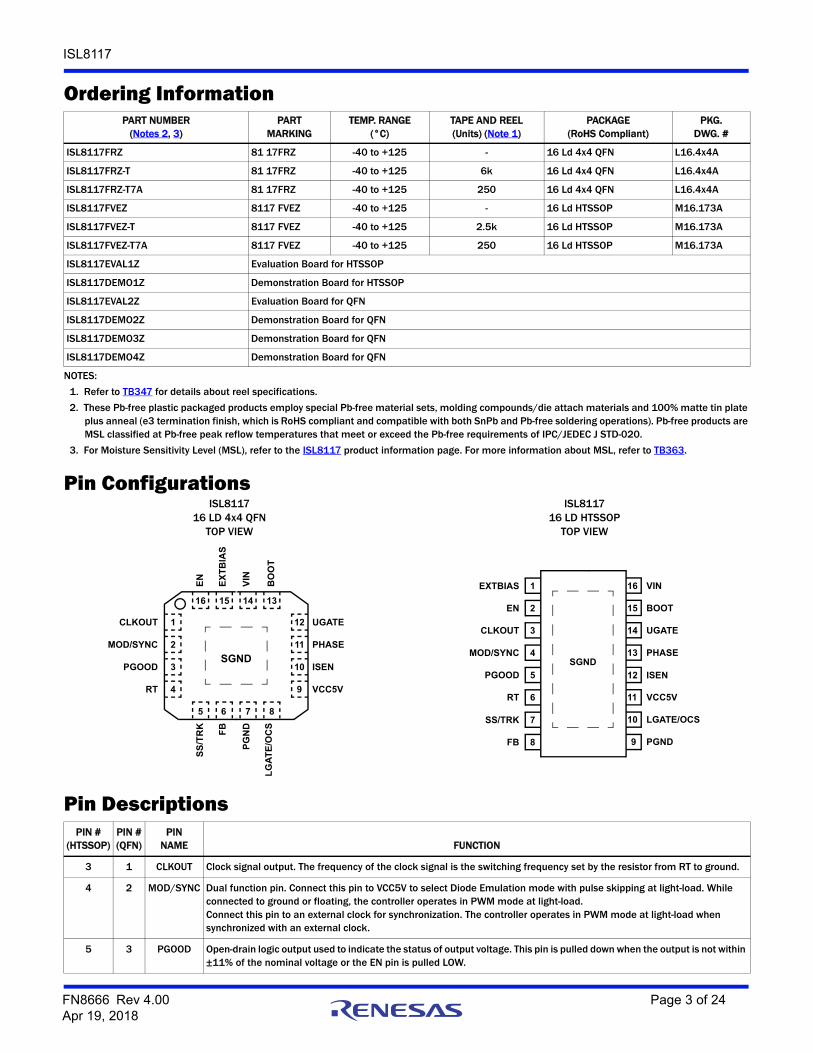
Pin ConfigurationsISL8117
16 LD 4x4 QFNTOP VIEW
ISL811716 LD HTSSOP
TOP VIEW
Ordering InformationPART NUMBER
(Notes 2, 3) PART
MARKINGTEMP. RANGE
(°C)TAPE AND REEL(Units) (Note 1)
PACKAGE(RoHS Compliant)
PKG.DWG. #
ISL8117FRZ 81 17FRZ -40 to +125 - 16 Ld 4x4 QFN L16.4x4A
ISL8117FRZ-T 81 17FRZ -40 to +125 6k 16 Ld 4x4 QFN L16.4x4A
ISL8117FRZ-T7A 81 17FRZ -40 to +125 250 16 Ld 4x4 QFN L16.4x4A
ISL8117FVEZ 8117 FVEZ -40 to +125 - 16 Ld HTSSOP M16.173A
ISL8117FVEZ-T 8117 FVEZ -40 to +125 2.5k 16 Ld HTSSOP M16.173A
ISL8117FVEZ-T7A 8117 FVEZ -40 to +125 250 16 Ld HTSSOP M16.173A
ISL8117EVAL1Z Evaluation Board for HTSSOP
ISL8117DEMO1Z Demonstration Board for HTSSOP
ISL8117EVAL2Z Evaluation Board for QFN
ISL8117DEMO2Z Demonstration Board for QFN
ISL8117DEMO3Z Demonstration Board for QFN
ISL8117DEMO4Z Demonstration Board for QFN
NOTES:
1. Refer to TB347 for details about reel specifications.
2. These Pb-free plastic packaged products employ special Pb-free material sets, molding compounds/die attach materials and 100% matte tin plate plus anneal (e3 termination finish, which is RoHS compliant and compatible with both SnPb and Pb-free soldering operations). Pb-free products are MSL classified at Pb-free peak reflow temperatures that meet or exceed the Pb-free requirements of IPC/JEDEC J STD-020.
3. For Moisture Sensitivity Level (MSL), refer to the ISL8117 product information page. For more information about MSL, refer to TB363.
1
3
4
15
CLKOUT
MOD/SYNC
PGOOD
RT
EN
EX
TB
IAS
VIN
BO
OT
16 14 13
2
12
10
9
11
65 7 8
UGATE
PHASE
ISEN
VCC5V
SS
/TR
K
FB
PG
ND
LG
AT
E/O
CS
SGND
14
15
16
9
13
12
11
10
1
2
3
4
5
7
6
8
EXTBIAS
EN
CLKOUT
MOD/SYNC
PGOOD
RT
FB
SS/TRK
VIN
UGATE
PHASE
ISEN
VCC5V
LGATE/OCS
PGND
BOOT
SGND
Pin DescriptionsPIN #
(HTSSOP)PIN #(QFN)
PINNAME FUNCTION
3 1 CLKOUT Clock signal output. The frequency of the clock signal is the switching frequency set by the resistor from RT to ground.
4 2 MOD/SYNC Dual function pin. Connect this pin to VCC5V to select Diode Emulation mode with pulse skipping at light-load. While connected to ground or floating, the controller operates in PWM mode at light-load.Connect this pin to an external clock for synchronization. The controller operates in PWM mode at light-load when synchronized with an external clock.
5 3 PGOOD Open-drain logic output used to indicate the status of output voltage. This pin is pulled down when the output is not within ±11% of the nominal voltage or the EN pin is pulled LOW.
FN8666 Rev 4.00 Page 3 of 24Apr 19, 2018
ISL8117
6 4 RT A resistor from this pin to ground adjusts the switching frequency from 100kHz to 2MHz. The switching frequency of the PWM controller is determined by the resistor, RT as shown in Equation 1.
Where fSW is the switching frequency in MHz.When this pin is tied to ground, the output frequency is set to 300kHz.When this pin is tied to VCC5V or floating, the output frequency is set to 600kHz.
7 5 SS/TRK Dual function pin. When used for soft-starting control, a soft-start capacitor is connected from this pin to ground. A regulated 2μA soft-starting current charges up the soft-start capacitor. Value of the soft-start capacitor sets the output voltage ramp.When used for tracking control, an external supply rail is configured as the master and the output voltage of the master supply is applied to this pin using a resistor divider. The output voltage will track the master supply voltage.
8 6 FB Output feedback input. Connect FB to a resistive voltage divider from the output to SGND to adjust the output voltage.
9 7 PGND Power ground connection. This pin should be connected to the sources of the lower MOSFETs and the (-) terminals of the external input capacitors.
10 8 LGATE/OCS Low-side MOSFET gate driver output and OC set pin. Connect a 1k to 30k resistor between this pin and ground to set the overcurrent threshold. If there is no resistor connected from this pin to GND, the overcurrent threshold is automatically set to the same point as a 10k resistor.
11 9 VCC5V Output of the internal 5V linear regulator. This output supplies bias for the IC, the low-side gate driver and the internal boot circuitry for the high-side gate driver. The VCC5V pin must always be decoupled to power ground with a minimum of 4.7µF ceramic capacitor placed very close to the pin. Do not allow the voltage at VCC5V to exceed VIN at any time. To prevent excessive current through the VCC5V pin to the VIN pin, a resistor can be connected from the VIN pin to the power supply.
12 10 ISEN Current sense signal input. This pin is used to monitor the voltage drop across the lower MOSFET for current loop feedback and overcurrent protection.
13 11 PHASE Phase node connection. This pin is connected to the junction of the upper MOSFET’s source, output filter inductor, and lower MOSFET’s drain.
14 12 UGATE High-side MOSFET gate driver output.
15 13 BOOT Bootstrap pin to provide bias for high-side driver. The positive terminal of the bootstrap capacitor connects to this pin. The bootstrap diode is integrated to help reduce total cost and reduce layout complexity.
16 14 VIN This pin should be tied to the input rail. It provides power to the internal linear drive circuitry and is also used by the feed-forward controller to adjust the amplitude of the PWM sawtooth. Decouple this pin with a small ceramic capacitor (0.1µF to 1µF) to ground.
1 15 EXTBIAS Input from an optional external 5V bias supply. There is an internal switch from this pin to VCC5V. This switch closes and supplies the IC power, bypassing the internal linear regulator, when voltage at EXTBIAS is higher than 4.7V (typ). Do not allow voltage at the EXTBIAS pin to exceed VIN at any time. To prevent excessive current through the EXTBIAS pin to the VIN pin, a resistor can be connected from the VIN pin to the power supply.Decouple this pin to ground with a small ceramic capacitor (0.1µF to 1µF) when it is in use, otherwise tie this pin to ground. DO NOT float this pin.
2 16 EN This pin provides an enable/disable function. The output is disabled when the pin is pulled to ground. When the voltage on the pin reaches 1.6V, the output becomes active. When the pin is floating, it will be enabled in default by internal pull-up.
- - SGNDEPAD
This is the small-signal ground common to all control circuitry. It is suggested to route this separately from the high current ground (PGND). SGND and PGND can be tied together if there is one solid ground plane with no noisy currents around the chip. All voltage levels are measured with respect to this pin.EPAD at ground potential. EPAD is connected to SGND internally. However, it is highly recommended to solder it directly to ground plane for better thermal performance and noise immunity.
Pin Descriptions (Continued)
PIN #(HTSSOP)
PIN #(QFN)
PINNAME FUNCTION
RT39.2fSW----------- 1.96– k= (EQ. 1)
FN8666 Rev 4.00 Page 4 of 24Apr 19, 2018
ISL8117
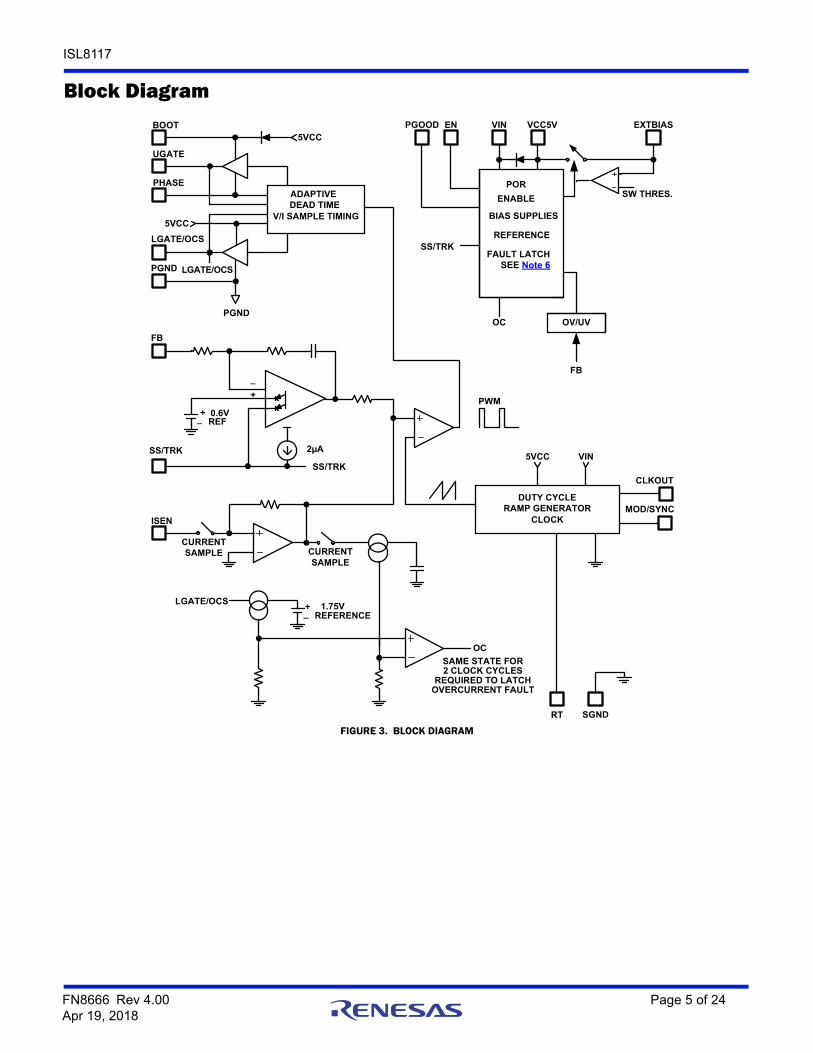
Block Diagram
5VCC
5VCCBOOT
UGATE
PHASE
LGATE/OCS
PGND
PGND
ADAPTIVE DEAD TIME
V/I SAMPLE TIMING
POR
ENABLE
BIAS SUPPLIES
REFERENCE
FAULT LATCH
OV/UVOC
FB
SW THRES.
PGOOD EN VIN VCC5V EXTBIAS
MOD/SYNC
FB
SS/TRK
ISEN
2µA
SS/TRK
SS/TRK
+
_
+_
0.6VREF
+_
1.75VREFERENCE
DUTY CYCLE RAMP GENERATOR
CLOCK
RT SGND
LGATE/OCS
LGATE/OCS
OC
CLKOUT
PWM
CURRENT SAMPLE CURRENT
SAMPLE
SAME STATE FOR2 CLOCK CYCLES
REQUIRED TO LATCHOVERCURRENT FAULT
VIN5VCC
SEE Note 6
FIGURE 3. BLOCK DIAGRAM
FN8666 Rev 4.00 Page 5 of 24Apr 19, 2018
ISL8117
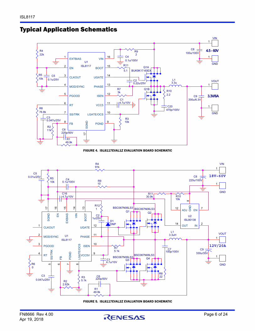
Typical Application Schematics
FIGURE 4. ISL8117EVAL1Z EVALUATION BOARD SCHEMATIC
FIGURE 5. ISL8117EVAL2Z EVALUATION BOARD SCHEMATIC
Q1ABUK9K17-60EX
C30.047u/25V
R92
3.3V/6A
VOUT1
R676.8k
C20470p/100V
R211k
GND
1
R510k
C9200u/6.3V
U1ISL8117
EXTBIAS1
EN2
CLKOUT3
MOD/SYNC4
PGOOD5
RT6
SS/TRK7
FB8
PGND9
LGATE/OCS10
VCC511
ISEN12
PHASE13
UGATE14
BOOT15
VIN16
SGN
D17
L13.3u
4.5 - 60V
VIN1
C14.7u/10V
R11
5.1
C50.1u/25V
Q1B R102.2
R73k
R422k
C40.1u/100V
C6220p/50V
C8100u/100V
R310k
R149.9k
GND
1
C20.22u/25V
18V~60V
12V/20A
R60
C8220u/100V
R121
Q2BSC067N06LS3
U2ISL80138
IN2
EN7
GN
D8
ADJ12
OUT14
VOUT1
C50.01u/25V
R149.9k
C14.7u/10V
R910
C7100p/100V
R491k
GND
1
R75.1k
Q3BSC067N06LS3
R510k
VIN1
R1010k
C6220p/50V
C9330u/35V
C40.1u/100V
R1130.9k
L13.3uH
Q1BSC067N06LS3
C30.047u/25V
U1ISL8117
CLKOUT1
MOD/SYNC2
PGOOD3
RT4
SS/T
RK
5
FB6
PGN
D7
LGAT
E/O
CS
8
VCC5V9
ISEN10
PHASE11
UGATE12
BOO
T13
VIN
14
EXBI
AS15
EN16
SGN
D17
R22.62k
R822
GND
1
D1DNP
Q4BSC067N06LS3
C21u/25V
C164.7u/10V
R35.1k
FN8666 Rev 4.00 Page 6 of 24Apr 19, 2018
ISL8117
Absolute Maximum Ratings Thermal InformationVCC5V to GND . . . . . . . . . . . . . . . . . . . . . . . . . . . . . . . . . . . . . . -0.3V to +5.9VEXTBIAS to GND . . . . . . . . . . . . . . . . . . . . . . . . . . . . . . . . . . . . -0.3V to +5.9VVIN to GND. . . . . . . . . . . . . . . . . . . . . . . . . . . . . . . . . . . . . . . . -0.3V to +62.5VBOOT/UGATE to PHASE . . . . . . . . . . . . . . . . . . . . . . . . -0.3V to VCC5V+0.3VPHASE and ISEN to GND . . . . . . . . . . . . . -5V (<20ns)/-0.3V (DC) to +62.5V EN, PGOOD, SS/TRK, FB to GND. . . . . . . . . . . . . . . . . -0.3V to VCC5V+0.3VLGATE/OCS to GND . . . . . . . . . . . . . . . . . . . . . . . . . . . -0.3V to VCC5V+0.3VRT, MOD/SYNC, CLKOUT to GND. . . . . . . . . . . . . . . . . -0.3V to VCC5V+0.3VVCC5V Short-Circuit to GND Duration. . . . . . . . . . . . . . . . . . . . . . . . . . . . . .1sESD Rating
Human Body Model (Tested per JS-001-2010) . . . . . . . . . . . . . . . . . . 4kVMachine Model (Tested per JESD22-A115C) . . . . . . . . . . . . . . . . . . 400VCharge Device Model (Tested per JESD22-C101E). . . . . . . . . . . . . . . 2kV
Latch-up (Tested per JESD78D; Class II, Level A, +125°C) . . . . . . . 100mA
Thermal Resistance (Typical) JA (°C/W) JC (°C/W)16 Ld QFN Package (Notes 4, 5) . . . . . . . . 40 2.516 Ld HTSSOP Package (Notes 4, 5) . . . . . 35 4.5
Maximum Junction Temperature . . . . . . . . . . . . . . . . . . . .-55°C to +150°CMaximum Operating Temperature . . . . . . . . . . . . . . . . . . .-40°C to +125°CMaximum Storage Temperature. . . . . . . . . . . . . . . . . . . . .-65°C to +150°CPb-Free Reflow Profile . . . . . . . . . . . . . . . . . . . . . . . . . . . . . . . . . . see TB493
Recommended Operating ConditionsTemperature . . . . . . . . . . . . . . . . . . . . . . . . . . . . . . . . . . . . .-40°C to +125°CVIN to GND. . . . . . . . . . . . . . . . . . . . . . . . . . . . . . . . . . . . . . . . . . . 4.5V to 60VVCC5V to GND . . . . . . . . . . . . . . . . . . . . . . . . . . . . . . . . . . . . . . . .-0.1V to 5.5VEXTBIAS to GND . . . . . . . . . . . . . . . . . . . . . . . . . . . . . . . . . . . . -0.1V to +5.5V
CAUTION: Do not operate at or near the maximum ratings listed for extended periods of time. Exposure to such conditions may adversely impact productreliability and result in failures not covered by warranty.
NOTES:
4. JA is measured in free air with the component mounted on a high-effective thermal conductivity test board with “direct attach” features. See TB379.
5. For JC, the “case temp” location is the center of the exposed metal pad on the package underside.
Electrical Specifications Recommended operating conditions unless otherwise noted. Refer to “Block Diagram” on page 5 and “Typical Application Schematics” on page 6. VIN = 4.5V to 60V, or VCC5V = 5V ±10%, C_VCC5V = 4.7µF, TA = -40°C to +125°C, Typical values are at TA = +25°C, unless otherwise specified. Boldface limits apply across the operating temperature range, -40°C to +125°C.
PARAMETER SYMBOL TEST CONDITIONSMIN
(Note 9) TYPMAX
(Note 9) UNIT
VIN SUPPLY
Input Voltage Range VIN 4.5 60.0 V
VIN SUPPLY CURRENT
Shutdown Current (Note 6) IVINQ EN = 0PGOOD is floating
5 10 µA
Operating Current (Note 8) IVINOP PGOOD is floating 2.5 4 mA
VCC5V SUPPLY (Note 6)
Operation Voltage VCC VIN = 12V, IL = 0mA 4.85 5.1 5.4 V
Internal LDO Output Voltage VIN = 4.5V, IL = 30mA 4.1 4.4 V
Internal LDO Output Voltage VIN > 5.6V, IL = 75mA 4.75 5.05 V
Maximum Supply Current of Internal LDO IVCC_MAX VVCC5V = 0V, VIN = 12V 120 mA
EXTBIAS SUPPLY (Note 6)
Switch Over Threshold Voltage, Rising VEXT_THR EXTBIAS voltage 4.5 4.7 4.9 V
Switch Over Threshold Voltage, Falling VEXT_THF EXTBIAS voltage 4.2 4.5 4.65 V
Internal Switch ON-resistance REXT VIN = 12V 1.5 Ω
UNDERVOLTAGE LOCKOUT
Undervoltage Lockout, Rising VUVLOTHR VIN voltage, 0mA on VCC5V 3.7 3.90 4.2 V
Undervoltage Lockout, Falling VUVLOTHF VIN voltage, 0mA on VCC5V 3.35 3.50 3.85 V
EN THRESHOLD
EN Rise Threshold VENSS_THR VIN > 5.6V 1.25 1.60 1.95 V
EN Fall Threshold VENSS_THF VIN > 5.6V 1.05 1.25 1.55 V
EN Hysteresis VENSS_HYST VIN > 5.6V 180 350 500 mV
SOFT-START CURRENT
SS/TRK Soft-Start Charge Current ISS SS/TRK = 0V 2.00 µA
FN8666 Rev 4.00 Page 7 of 24Apr 19, 2018

ISL8117
DEFAULT INTERNAL MINIMUM SOFT-STARTING
Default Internal Output Ramping Time tSS_MIN SS/TRK open 1.5 ms
POWER-GOOD MONITORS
PGOOD Upper Threshold VPGOV 109 112.5 115 %
PGOOD Lower Threshold VPGUV 85 87.5 92 %
PGOOD Low Level Voltage VPGLOW I_SINK = 2mA 0.35 V
PGOOD Leakage Current IPGLKG PGOOD = 5V 20 150 nA
PGOOD TIMING
VOUT Rising Threshold to PGOOD Rising (Note 11) tPGR 1.1 5 ms
VOUT Falling Threshold to PGOOD Falling tPGF 75 µs
REFERENCE SECTION
Internal Reference Voltage VREF 0.600 V
Reference Voltage Accuracy TA = 0°C to +85°C -0.75 +0.75 %
TA = -40°C to +125°C -1.00 +1.00 %
FB Bias Current IFBLKG -40 0 40 nA
PWM CONTROLLER ERROR AMPLIFIERS
DC Gain 88 dB
Gain-BW Product GBW 8 MHz
Slew Rate SR 2.0 V/µs
PWM REGULATOR
Minimum Off Time tOFF_MIN 308 ns
Minimum On Time tON_MIN 40 ns
Peak-to-Peak Sawtooth Amplitude DVRAMP VIN = 20V 1.0 V
VIN = 12.0V 0.6 V
Ramp Offset 1.0 V
SWITCHING FREQUENCY
Switching Frequency fSW RT = 36k 890 1050 1195 kHz
Switching Frequency RT = 16.5k 1650 2000 2375 kHz
Switching Frequency RT PIN connect to GND 250 300 350 kHz
Switching Frequency RT PIN connect to VCC5V or FLOAT 515 600 645 kHz
RT Voltage VRT RT = 36k 770 mV
CLOCK OUTPUT AND SYNCHRONIZATION
CLKOUT Output High VCLKH ISOURCE = 1mA VCC5V - 0.3
V
CLKOUT Output Low VCLKL ISINK = 1mA 0.3 V
CLKOUT Frequency fCLK RT = VCC5V 515 600 645 kHz
SYNC Synchronization Range fSYNC RT = 36kΩ 1230 2200 kHz
DIODE EMULATION MODE DETECTION
MOD/SYNC Threshold High VMODETHH 1.1 1.6 2.1 V
MOD/SYNC Hysteresis VMODEHYST 200 mV
Diode Emulation Phase Threshold (Note 10) VCROSS VIN = 12V -3 mV
Electrical Specifications Recommended operating conditions unless otherwise noted. Refer to “Block Diagram” on page 5 and “Typical Application Schematics” on page 6. VIN = 4.5V to 60V, or VCC5V = 5V ±10%, C_VCC5V = 4.7µF, TA = -40°C to +125°C, Typical values are at TA = +25°C, unless otherwise specified. Boldface limits apply across the operating temperature range, -40°C to +125°C. (Continued)
PARAMETER SYMBOL TEST CONDITIONSMIN
(Note 9) TYPMAX
(Note 9) UNIT
FN8666 Rev 4.00 Page 8 of 24Apr 19, 2018
ISL8117
PWM GATE DRIVER
Source Current IGSRC 2000 mA
Sink Current IGSNK 2000 mA
Upper Drive Pull-Up RUG_UP VCC5V = 5.0V 1.5 Ω
Upper Drive Pull-Down RUG_DN VCC5V = 5.0V 1.5 Ω
Lower Drive Pull-Up RLG_UP VCC5V = 5.0V 1.0 Ω
Lower Drive Pull-Down RLG_DN VCC5V = 5.0V 0.8 Ω
Upper Drive Rise Time tGR_UP COUT = 1000pF 9.0 ns
Upper Drive Fall Time tGF_UP COUT = 1000pF 8.0 ns
Lower Drive Rise Time tGR_DN COUT = 1000pF 7.0 ns
Lower Drive Fall Time tGF_DN COUT = 1000pF 6.1 ns
OVERVOLTAGE PROTECTION
OVP Threshold VOVTH 116 121 127 %
OVERCURRENT PROTECTION
OC Set Current Source IOCSET-CS LGATE/OCS = 0V 9 10.5 11.5 µA
OVER-TEMPERATURE
Over-Temperature Shutdown TOT-TH 160 °C
Over-Temperature Hysteresis TOT-HYS 15 °C
NOTES:
6. In normal operation, where the device is supplied with voltage on the VIN pin, the VCC5V pin provides a 5V output capable of 75mA (min). When the device is supplied by an external 5V supply on the EXTBIAS pin, the internal LDO regulator is disabled. The voltage at VCC5V should not exceed the voltage at VIN at any time. (Refer to “Pin Descriptions” on page 3 for more details.)
7. This is the total shutdown current with VIN = 5.6V and 60V.
8. Operating current is the supply current consumed when the device is active but not switching. It does not include gate drive current.
9. Parameters with MIN and/or MAX limits are 100% tested at +25°C, unless otherwise specified. Temperature limits established by characterization and are not production tested.
10. Threshold voltage at PHASE pin for turning off the bottom MOSFET during DEM.
11. When soft-start time is less than 4.5ms, tPGR increases. With internal soft-start (the fastest soft-start time), tPGR increases close to its max limit 5ms.
Electrical Specifications Recommended operating conditions unless otherwise noted. Refer to “Block Diagram” on page 5 and “Typical Application Schematics” on page 6. VIN = 4.5V to 60V, or VCC5V = 5V ±10%, C_VCC5V = 4.7µF, TA = -40°C to +125°C, Typical values are at TA = +25°C, unless otherwise specified. Boldface limits apply across the operating temperature range, -40°C to +125°C. (Continued)
PARAMETER SYMBOL TEST CONDITIONSMIN
(Note 9) TYPMAX
(Note 9) UNIT
FN8666 Rev 4.00 Page 9 of 24Apr 19, 2018

ISL8117
Typical Performance Curves Oscilloscope plots are taken using the ISL8117EVAL2Z evaluation board, VIN = 18 to 60V, VOUT = 12V, IOUT = 20A unless otherwise noted.
FIGURE 6. SHUTDOWN CURRENT vs TEMPERATURE FIGURE 7. QUIESCENT CURRENT vs TEMPERATURE
FIGURE 8. VCC5V LOAD REGULATION FIGURE 9. VCC5V LINE REGULATION
FIGURE 10. SWITCHING FREQUENCY vs TEMPERATURE (RT = 36kΩ) FIGURE 11. SWITCHING FREQUENCY vs VIN
TEMPERATURE (°C)
I VIN
Q (
µA
)
0
1
2
3
4
5
6
7
8
9
10
-40 -25 -10 5 20 35 50 65 80 95 110 125
I VIN
OP (
mA
)
TEMPERATURE (°C)
0
0.5
1.0
1.5
2.0
2.5
3.0
3.5
4.0
4.5
5.0
-40 -25 -10 5 20 35 50 65 80 95 110 125
0
1
2
3
4
5
6
0 20 40 60 80 100 120
LOAD CURRENT (mA)
VC
C5
V (
V)
4.4
4.5
4.6
4.7
4.8
4.9
5.0
5.1
5.2
0 10 20 30 40 50 60
VIN (V)
VC
C5
V (
V)
f SW
(k
Hz)
TEMPERATURE (°C)
1000
1010
1020
1030
1040
1050
1060
1070
1080
1090
1100
-40 -25 -10 5 20 35 50 65 80 95 110 125
VIN (V)
f SW
(k
Hz)
0
50
100
150
200
250
300
350
0 5 10 15 20 25 30 35 40 45 50 55 60
FN8666 Rev 4.00 Page 10 of 24Apr 19, 2018
ISL8117
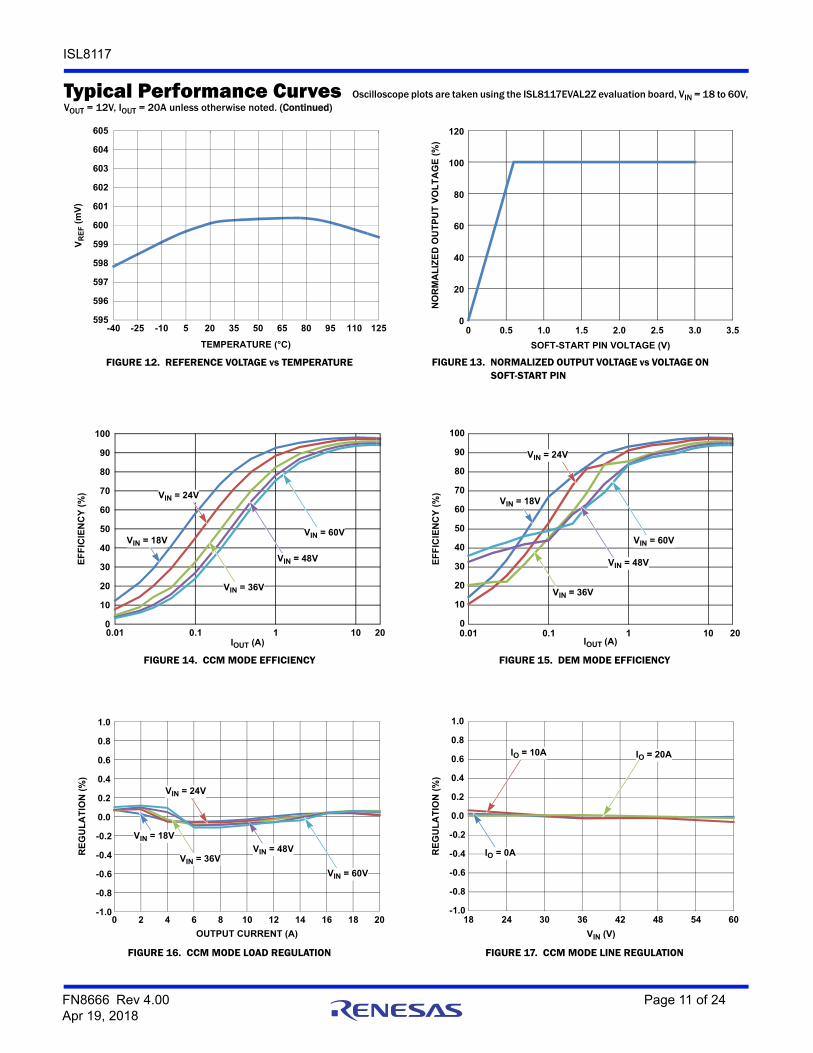
FIGURE 12. REFERENCE VOLTAGE vs TEMPERATURE FIGURE 13. NORMALIZED OUTPUT VOLTAGE vs VOLTAGE ON SOFT-START PIN
FIGURE 14. CCM MODE EFFICIENCY FIGURE 15. DEM MODE EFFICIENCY
FIGURE 16. CCM MODE LOAD REGULATION FIGURE 17. CCM MODE LINE REGULATION
Typical Performance Curves Oscilloscope plots are taken using the ISL8117EVAL2Z evaluation board, VIN = 18 to 60V, VOUT = 12V, IOUT = 20A unless otherwise noted. (Continued)
VR
EF (
mV
)
TEMPERATURE (°C)
595
596
597
598
599
600
601
602
603
604
605
-40 -25 -10 5 20 35 50 65 80 95 110 1250
20
40
60
80
100
120
0 0.5 1.0 1.5 2.0 2.5 3.0 3.5
SOFT-START PIN VOLTAGE (V)
NO
RM
AL
IZE
D O
UT
PU
T V
OL
TA
GE
(%
)
0
10
20
30
40
50
60
70
80
90
100
0.01 0.1 1 10
VIN = 18V
VIN = 24V
VIN = 36V
VIN = 48V
VIN = 60V
IOUT (A)
EF
FIC
IEN
CY
(%
)
200
10
20
30
40
50
60
70
80
90
100
0.01 0.1 1 10IOUT (A)
EF
FIC
IEN
CY
(%
)
VIN = 18V
VIN = 24V
VIN = 36V
VIN = 48V
VIN = 60V
20
-1.0
-0.8
-0.6
-0.4
-0.2
0.0
0.2
0.4
0.6
0.8
1.0
0 2 4 6 8 10 12 14 16 18 20
OUTPUT CURRENT (A)
RE
GU
LA
TIO
N (
%)
VIN = 36VVIN = 48V
VIN = 60V
VIN = 18V
VIN = 24V
-1.0
-0.8
-0.6
-0.4
-0.2
0.0
0.2
0.4
0.6
0.8
1.0
18 24 30 36 42 48 54 60
IO = 20A
VIN (V)
RE
GU
LA
TIO
N (
%)
IO = 10A
IO = 0A
FN8666 Rev 4.00 Page 11 of 24Apr 19, 2018
ISL8117
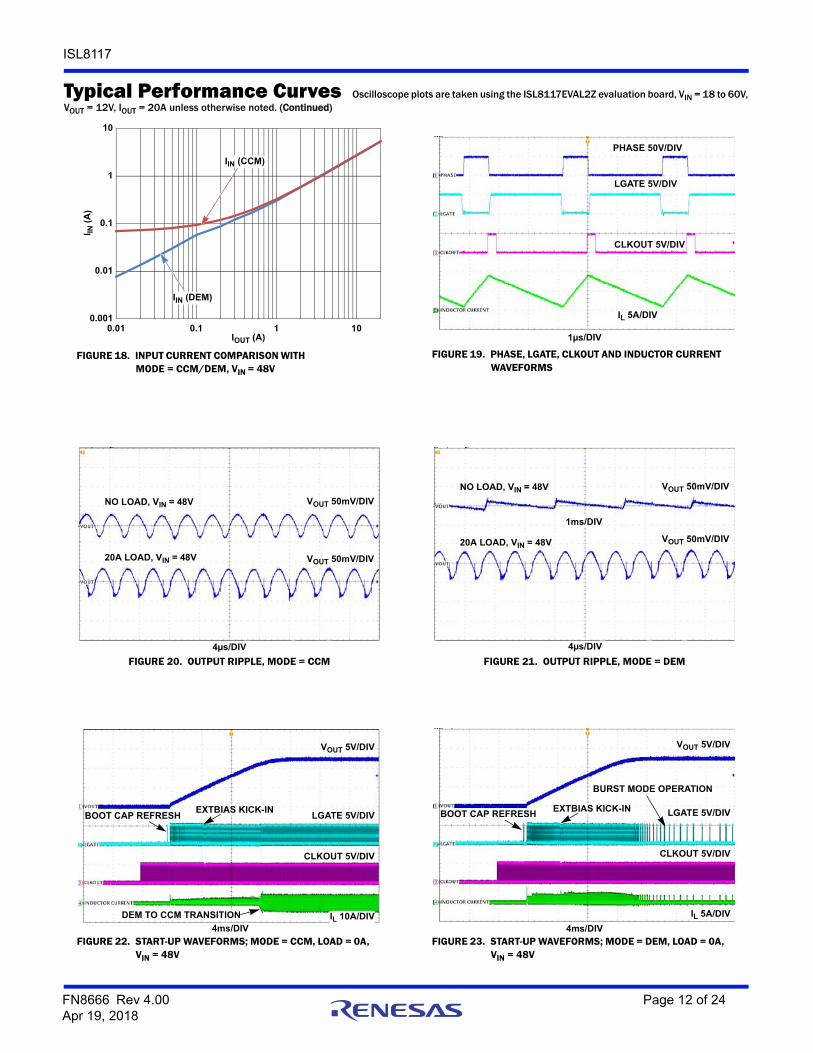
FIGURE 18. INPUT CURRENT COMPARISON WITH MODE = CCM/DEM, VIN = 48V
FIGURE 19. PHASE, LGATE, CLKOUT AND INDUCTOR CURRENT WAVEFORMS
FIGURE 20. OUTPUT RIPPLE, MODE = CCM FIGURE 21. OUTPUT RIPPLE, MODE = DEM
FIGURE 22. START-UP WAVEFORMS; MODE = CCM, LOAD = 0A, VIN = 48V
FIGURE 23. START-UP WAVEFORMS; MODE = DEM, LOAD = 0A, VIN = 48V
Typical Performance Curves Oscilloscope plots are taken using the ISL8117EVAL2Z evaluation board, VIN = 18 to 60V, VOUT = 12V, IOUT = 20A unless otherwise noted. (Continued)
0.001
0.01
0.1
1
10
0.01 0.1 1 10
IIN (DEM)
IIN (CCM)
I IN (
A)
IOUT (A)
IL 5A/DIV
LGATE 5V/DIV
CLKOUT 5V/DIV
PHASE 50V/DIV
1µs/DIV
4µs/DIV
VOUT 50mV/DIV
VOUT 50mV/DIV
NO LOAD, VIN = 48V
20A LOAD, VIN = 48V
4µs/DIV
VOUT 50mV/DIV
VOUT 50mV/DIV
NO LOAD, VIN = 48V
20A LOAD, VIN = 48V
1ms/DIV
4ms/DIV
VOUT 5V/DIV
LGATE 5V/DIV
CLKOUT 5V/DIV
IL 10A/DIVDEM TO CCM TRANSITION
EXTBIAS KICK-INBOOT CAP REFRESH
4ms/DIV
VOUT 5V/DIV
LGATE 5V/DIV
CLKOUT 5V/DIV
IL 5A/DIV
EXTBIAS KICK-INBOOT CAP REFRESH
BURST MODE OPERATION
FN8666 Rev 4.00 Page 12 of 24Apr 19, 2018
ISL8117
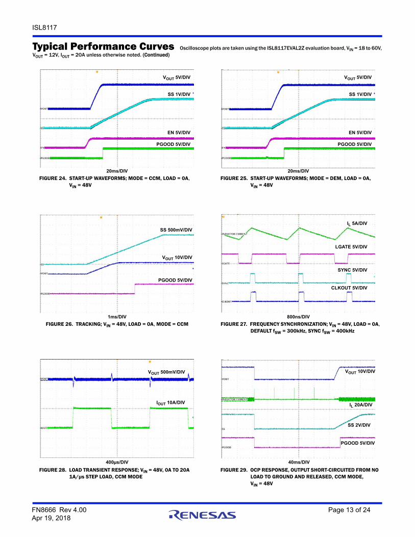
FIGURE 24. START-UP WAVEFORMS; MODE = CCM, LOAD = 0A,VIN = 48V
FIGURE 25. START-UP WAVEFORMS; MODE = DEM, LOAD = 0A,VIN = 48V
FIGURE 26. TRACKING; VIN = 48V, LOAD = 0A, MODE = CCM FIGURE 27. FREQUENCY SYNCHRONIZATION; VIN = 48V, LOAD = 0A, DEFAULT fSW = 300kHz, SYNC fSW = 400kHz
FIGURE 28. LOAD TRANSIENT RESPONSE; VIN = 48V, 0A TO 20A 1A/µs STEP LOAD, CCM MODE
FIGURE 29. OCP RESPONSE, OUTPUT SHORT-CIRCUITED FROM NO LOAD TO GROUND AND RELEASED, CCM MODE, VIN = 48V
Typical Performance Curves Oscilloscope plots are taken using the ISL8117EVAL2Z evaluation board, VIN = 18 to 60V, VOUT = 12V, IOUT = 20A unless otherwise noted. (Continued)
20ms/DIV
VOUT 5V/DIV
SS 1V/DIV
EN 5V/DIV
PGOOD 5V/DIV
20ms/DIV
VOUT 5V/DIV
SS 1V/DIV
EN 5V/DIV
PGOOD 5V/DIV
1ms/DIV
SS 500mV/DIV
VOUT 10V/DIV
PGOOD 5V/DIV
800ns/DIV
IL 5A/DIV
LGATE 5V/DIV
SYNC 5V/DIV
CLKOUT 5V/DIV
400µs/DIV
VOUT 500mV/DIV
IOUT 10A/DIV
40ms/DIV
VOUT 10V/DIV
IL 20A/DIV
SS 2V/DIV
PGOOD 5V/DIV
FN8666 Rev 4.00 Page 13 of 24Apr 19, 2018

ISL8117
Functional DescriptionGeneral DescriptionThe ISL8117 integrates control circuits for a synchronous buck converter. The driver and protection circuits are also integrated to simplify the end design.
The part has an independent enable/disable control line EN, which provides a flexible power-up sequencing and a simple VIN UVP implementation. The soft-start time is programmable by adjusting the soft-start capacitor connected from SS/TRK.
The valley current mode control scheme with input voltage feed-forward ramp simplifies loop compensation and provides excellent rejection to input voltage variation.
Input Voltage RangeThe ISL8117 is designed to operate from input supplies ranging from 4.5V to 60V.
The input voltage range can be effectively limited by the available minimum PWM off-time as shown in Equation 2.
where,Vd1 = sum of the parasitic voltage drops in the inductor discharge path, including the lower FET, inductor and PC board.Vd2 = sum of the voltage drops in the charging path, including the upper FET, inductor and PC board resistances.tOFF(min) = 308ns.
The maximum input voltage and minimum output voltage is limited by the minimum on-time (tON(min)) as shown in Equation 3.
where, tON(min) = 40ns in CCM and 60ns in DEM.
Internal 5V Linear Regulator (VCC5V) and External VCC Bias Supply (EXTBIAS)All the ISL8117 functions can be internally powered from an on-chip, low dropout 5V regulator or an external 5V bias voltage through the EXTBIAS pin. Bypass the linear regulator’s output (VCC5V) with a 4.7µF capacitor to the power ground. The ISL8117 also employs an undervoltage lockout circuit, which disables all regulators when VCC5V falls below 3.5V.
The internal LDO can source over 75mA to supply the IC, power the low-side gate driver, and charge the boot capacitor. When driving large FETs at high switching frequency, little or no regulator current may be available for external loads.
For example, a single large FET with 15nC total gate charge requires 15nC x 300kHz = 4.5mA (15nC x 600kHz = 9mA). Also, at higher input voltages with larger FETs, the power dissipation across the internal 5V will increase. Excessive dissipation across this regulator must be avoided to prevent junction temperature
rise. Thermal protection may be triggered if die temperature increases above +160°C due to excessive power dissipation.
When large MOSFETs are used, an external 5V bias voltage can be applied to the EXTBIAS pin to alleviate excessive power dissipation. Voltage at the EXTBIAS pin must always be lower than the voltage at the VIN pin to prevent biasing of the power stage through EXTBIAS and VCC5V. An external UVLO circuit might be necessary to ensure smooth soft-starting.
The internal LDO has an overcurrent limit of typically 120mA. For better efficiency, connect VCC5V to VIN for 5V ±10% input applications.
Enable and Soft-Start OperationPulling the EN pin high or low can enable or disable the controller. When the EN pin voltage is higher than 1.6V, the controller is enabled to initialize its internal circuit. After the VCC5V pin reaches the UVLO threshold, ISL8117 soft-start circuitry becomes active. The internal 2µA charge current begins charging up the soft-start capacitor connected from the SS/TRK pin to GND. The voltage error amplifier reference voltage is clamped to the voltage on the SS/TRK pin. The output voltage thus rises from 0V to regulation as SS/TRK rises from 0V to 0.6V. Charging of the soft-start capacitor continues until the voltage on the SS/TRK pin reaches 3V.
Typical applications for ISL8117 use programmable analog soft-start or SS/TRK pin for tracking. The soft-start time can be set by the value of the soft-start capacitor connected from the SS/TRK to GND. Inrush current during start-up can be alleviated by adjusting the soft-starting time.
The typical soft-start time is set according to Equation 4:
When the soft-starting time set by external CSS or tracking is less than 1.5ms, an internal soft-start circuit of 1.5ms takes over the soft-start.
PGOOD will toggle to high when the corresponding output is up and in regulation.
Pulling the EN low disables the PWM output and internal LDO to achieve low standby current. The SS/TRK pin will also be discharged to GND by an internal MOSFET with 70Ω rDS(ON).
Output Voltage ProgrammingThe ISL8117 provides a precision 0.6V internal reference voltage to set the output voltage. Based on this internal reference, the output voltage can be set from 0.6V up to a level determined by the input voltage, the maximum duty cycle, and the conversion efficiency of the circuit.
A resistive divider from the output to ground sets the output voltage. The center point of the divider shall be connected to the FB pin. The output voltage value is determined by Equation 5.
where R1 is the top resistor of the feedback divider network and R2 is the bottom resistor connected from FB to ground.
VIN min
VOUT Vd1+
1 t– OFF min Frequency--------------------------------------------------------------------------
Vd2 Vd1–+ (EQ. 2)
VIN max
VOUTtON min Frequency--------------------------------------------------------------
(EQ. 3)
tSS 0.6VCSS2A----------- = (EQ. 4)
VOUT 0.6VR1 R2+
R2---------------------
= (EQ. 5)
FN8666 Rev 4.00 Page 14 of 24Apr 19, 2018

ISL8117
Tracking OperationThe ISL8117 can be set up to track an external supply. To implement tracking, a resistive divider is connected between the external supply output and ground. The center point of the divider shall be connected to the SS/TRK pin of the ISL8117. The resistive divider ratio sets the ramping ratio between the two voltage rails. To implement coincident tracking, set the tracking resistive divider ratio exactly the same as the ISL8117 output resistive divider given by Equation 5. Make sure that the voltage at SS/TRK is greater than 0.6V when the master rail reaches regulation.
To minimize the impact of the 2µA soft-start current on the tracking function, it is recommended to use resistors of less than 10kΩ for the tracking resistive divider.
When overcurrent protection (OCP) is triggered, the internal minimum soft-start circuit determines the OCP soft-start hiccup.
Light-Load Efficiency EnhancementWhen MOD/SYNC is tied to VCC5V, the ISL8117 operates in high efficiency Diode Emulation mode and Pulse Skipping mode in light-load condition. The inductor current is not allowed to reverse (discontinuous operation). At very light-loads, the converter goes into diode emulation and triggers the pulse skipping function. In Pulse Skipping mode, the upper MOSFET remains off until the output voltage drops to the point the error amplifier output goes above the pulse skipping mode threshold. The minimum tON in the pulse skipping mode is 60ns.
Prebiased Power-UpThe ISL8117 has the ability to soft-start with a prebiased output. The output voltage would not be pulled down during prebiased start-up. The PWM is not active until the soft-start ramp reaches the output voltage times the resistive divider ratio.
Overvoltage protection is alive during soft-start.
Frequency SelectionSwitching frequency selection is a trade-off between efficiency and component size. Low switching frequency improves efficiency by reducing MOSFET switching loss. To meet the output ripple and load transient requirements, operation at a low switching frequency would require larger inductance and output capacitance. The switching frequency of the ISL8117 is set by a resistor connected from the RT pin to GND according to Equation 1.
The frequency setting curve shown in Figure 30 assists in selecting the correct value for RT.
Frequency SynchronizationThe MOD/SYNC pin may be used to synchronize ISL8117 to an external clock or the CLKOUT pin of another ISL8117. When the MOD/SYNC pin is connected to the CLKOUT pin of another ISL8117, the two controllers operate in synchronization.
When the MOD/SYNC pin is connected to an external clock, the ISL8117 will synchronize to this external clock frequency. For proper operation, the frequency set by resistor RT should be lower than the external clock frequency.
When frequency synchronization is in action, the controllers will enter forced continuous current mode at light-load.
CLKOUT pin outputs a clock signal with a 280ns pulse width. The signal frequency is the same as the frequency set by the resistor from RT pin to ground. The signal rising edge is in line with the PWM falling edge.
Gate Control LogicThe gate control logic translates the PWM signal into gate drive signals providing amplification, level shifting, and shoot-through protection. The gate driver has circuitry that helps optimize the IC performance over a wide range of operational conditions. MOSFET switching times can vary dramatically from type to type and with input voltage, the gate control logic provides adaptive dead time by monitoring real gate waveforms of both the upper and the lower MOSFETs. Shoot-through control logic provides a 16ns dead time to ensure that both the upper and lower MOSFETs will not turn on simultaneously causing a shoot-through condition.
FIGURE 30. RT vs SWITCHING FREQUENCY fSW
0
500
1000
1500
2000
2500
3000
3500
0 20 40 60 80 100 120 140 160 180 200
RT (kΩ)
f SW
(k
Hz)
FN8666 Rev 4.00 Page 15 of 24Apr 19, 2018

ISL8117
Gate DriverThe low-side gate driver is supplied from VCC5V and provides a 2A peak sink and source current. The high-side gate driver is also capable of delivering the same currents as the low-side gate driver. Gate-drive voltage for the upper N-channel MOSFET is generated by a flying capacitor boot circuit. A boot capacitor connected from the BOOT pin to the PHASE node provides power to the high-side MOSFET driver. To limit the peak current in the IC, an external resistor can be placed between the BOOT pin and the boot capacitor. This small series resistor also damps any oscillations caused by the resonant tank of the parasitic inductances in the traces of the board and the FET’s input capacitance.
At start-up, the low-side MOSFET turns on first and forces PHASE to ground in order to charge the BOOT capacitor to 5V. After the low-side MOSFET turns off, the high-side MOSFET is turned on by closing an internal switch between BOOT and UGATE. This provides the necessary gate-to-source voltage to turn on the upper MOSFET, an action that boosts the 5V gate drive signal above VIN. The current required to drive the upper MOSFET is drawn from the internal 5V regulator.
For optimal EMI performance or reducing phase node ringing, a small resistor might be placed between the BOOT pin to the positive terminal of the bootstrap capacitor.
Adaptive Dead Time The ISL8117 incorporates an adaptive dead time algorithm on the synchronous buck PWM controller that optimizes operation with varying MOSFET conditions. This algorithm provides approximately 16ns dead time between the switching of the upper and lower MOSFETs. This dead time is adaptive and allows operation with different MOSFETs without having to externally adjust the dead time using a resistor or capacitor. During turn-off of the lower MOSFET, the LGATE voltage is monitored until it reaches a threshold of 1V, at which time the UGATE is released to rise. Adaptive dead time circuitry monitors the upper MOSFET gate voltage during UGATE turn-off. Once the upper MOSFET gate-to-source voltage has dropped below a threshold of 1V, the LGATE is allowed to rise. It is recommended to not use a resistor between UGATE and LGATE and the respective MOSFET gates as it may interfere with the dead time circuitry.
Internal Bootstrap Diode The ISL8117 has an integrated bootstrap diode to help reduce total cost and reduce layout complexity. Simply adding an external capacitor across the BOOT and PHASE pins completes the bootstrap circuit. The bootstrap capacitor can be chosen from Equation 6.
where QGATE is the amount of gate charge required to fully charge the gate of the upper MOSFET. The VBOOT term is defined as the allowable droop in the rail of the upper drive.
As an example, suppose an upper MOSFET has a gate charge (QGATE) of 25nC at 5V and also assume the droop in the drive voltage over a PWM cycle is 200mV. Based on the calculation, a bootstrap capacitance of at least 0.125µF is required. The next larger standard value capacitance of 0.22µF should be used. A good quality ceramic capacitor is recommended.
The internal bootstrap Schottky diode has a resistance of 1.5Ω (typical) at 800mA. Combined with the resistance RBOOT, this could lead to the boot capacitor charging insufficiently in cases where the bottom MOSFET is turned on for a very short period of time. If such circumstances are expected, an additional external Schottky diode may be added from VCC5V to the positive of the boot capacitor. RBOOT may still be necessary to lower EMI due to fast turn-on of the upper MOSFET.
Power-Good IndicatorThe power-good pin can be used to monitor the status of the output voltage. PGOOD will be true (open drain) 1.1ms after the FB pin is within ±11% of the reference voltage.
There is no extra delay when the PGOOD pin is pulled LOW.
Protection CircuitsThe converter output is monitored and protected against overload, light-load, and undervoltage conditions.
Undervoltage Lockout The ISL8117 includes UVLO protection, which keeps the device in a reset condition until a proper operating voltage is applied. It also shuts down the ISL8117 if the operating voltage drops below a predefined value. The controller is disabled when UVLO is asserted. When UVLO is asserted, PGOOD is valid and will be deasserted.
BOOT
UGATE
PHASE
VCC_5VVIN
ISL8117
FIGURE 31. UPPER GATE DRIVER CIRCUIT
CB
RBOOT
OPTIONALEXTERNALSCHOTTKY
BOOT
QGATEVBOOT------------------------ (EQ. 6)
FN8666 Rev 4.00 Page 16 of 24Apr 19, 2018
ISL8117
Overcurrent ProtectionThe controller uses the lower MOSFET's ON-resistance, rDS(ON), to monitor the current in the converter. The sensed voltage drop is compared with a threshold set by a resistor, ROCSET, connected from the LGATE/OCS pin to ground during the initiation stage before soft-start. During the initiation stage, a 10.5µA current source from LGATE/OCS pin creates a voltage drop on ROCSET. The voltage drop is then read and stored as the OCP comparator reference. ROCSET can be calculated by Equation 7.
where IOC is the desired overcurrent protection threshold and RCS is the value of the current sense resistor connected to the ISEN pin. The unit for rDS(ON) is mΩ and for RCS it is kΩ.
If an overcurrent is detected, the upper MOSFET remains off and the lower MOSFET remains on until the next cycle. As a result, the converter will skip a pulse. When the overload condition is removed, the converter will resume normal operation.
If an overcurrent is detected for two consecutive clock cycles, the IC enters in a Hiccup mode by turning off the gate driver and entering soft-start. The IC will stay off for 50ms before trying to restart. The IC will continue to cycle through soft-start until the overcurrent condition is removed. Hiccup mode is active during soft-start, so care must be taken to ensure that the peak inductor current does not exceed the overcurrent threshold during soft-start.
Because of the nature of this current sensing technique, and to accommodate a wide range of rDS(ON) variations, the value of the overcurrent threshold should represent an overload current about 150% to 180% of the maximum operating current. If more accurate current protection is desired, place a current sense resistor in series with the lower MOSFET source.
When OCP is triggered, the SS/TRK pin is pulled to ground by an internal MOSFET for hiccup restart. When configured to track another voltage rail, the SS/TRK pin rises up much faster than the internal minimum soft-start ramp. The voltage reference will then be clamped to the internal minimum soft-start ramp. Thus, smooth soft-start hiccup is achieved even with the tracking function.
For applications with large inductor ripple current, it is recommended to use a larger RCS to reduce the current ripple into the ISEN pin to less than 6µA which is the OCP comparator hysteresis. Otherwise, when the load current approaches to the OCP trip point, the OCP comparator can trip and reset in one switching cycle. The overcurrent condition cannot last for two consecutive cycles to force the IC into Hiccup mode. Instead, the IC will run in a half frequency PWM mode leading to a larger output ripple.
Overvoltage ProtectionThe overvoltage set point is set at 121% of the nominal output voltage set by the feedback resistors. In the case of an overvoltage event, the IC will attempt to bring the output voltage back into regulation by keeping the upper MOSFET turned off and the lower MOSFET turned on. If the overvoltage condition has been corrected and the output voltage returns to 110% of the
nominal output voltage, both upper and lower MOSFETs will be turned off until the output voltage drops to the nominal voltage to start work in normal PWM switching.
For lower control loop bandwidth applications, such as very low output voltage or very low switching frequency designs, the full load to no load transient response may be slow to cause an OVP false trigger. When OVP is triggered, the long LGATE on-time will create a high negative inductor current leading to a higher than normal sink in current to the ISEN pin. It is recommended to limit the ISEN pin sink in current to less than 16µA. Otherwise, a false OCP hiccup operation may be triggered to cause the output to shut down.
Over-Temperature ProtectionThe IC incorporates an over-temperature protection circuit that shuts the IC down when a die temperature of +160°C is reached. Normal operation resumes when the die temperature drops below +145°C through the initiation of a full soft-start cycle. During OTP shutdown, the IC consumes only 100µA of current. When the controller is disabled, thermal protection is inactive; this helps achieve a very low shutdown current of 5µA.
Feedback Loop CompensationTo reduce the number of external components and to simplify the process of determining compensation components, the controller is designed with an internally compensated error amplifier. To make internal compensation possible, several design measures were taken.
First, the ramp signal applied to the PWM comparator is proportional to the input voltage provided at the VIN pin. This keeps the modulator gain constant with varying input voltages. Next, the load current proportional signal is derived from the voltage drop across the lower MOSFET during the PWM time interval and is subtracted from the amplified error signal on the comparator input. This creates an internal current control loop. The resistor RCS connected to the ISEN pin sets the gain in the current feedback loop. The following expression estimates the required value of the current sense resistor depending on the maximum operating load current and the value of the MOSFET rDS(ON) as shown in Equation 8.
Choosing RCS to provide 30µA of current to the current sample and hold circuitry is recommended but values down to 2µA and up to 100µA can be used.
Due to the current loop feedback, the modulator has a single pole response with -20dB slope at a frequency determined by the load by using Equation 9.
where RO is load resistance and CO is load capacitance. For this type of modulator, a Type 2 compensation circuit is usually sufficient.
Figure 32 on page 18 shows a Type 2 amplifier and its response, along with the responses of the current mode modulator and the
ROCSET
rDS ON IOC
0.7 3.5RCS+------------------------------------------- k = (EQ. 7)
RCS
IMAX rDS ON
30A----------------------------------------------- (EQ. 8)
FPO1
2 RO CO --------------------------------- = (EQ. 9)
FN8666 Rev 4.00 Page 17 of 24Apr 19, 2018

ISL8117
converter. The Type 2 amplifier, in addition to the pole at origin, has a zero-pole pair that causes a flat gain region at frequencies between the zero and the pole.
High amplifier zero frequency gain and modulator gain are chosen to satisfy most typical applications. The crossover frequency will appear at the point where the modulator attenuation equals the amplifier high frequency gain. The only task that the system designer has to complete is to specify the output filter capacitors to position the load main pole somewhere within one decade lower than the amplifier zero frequency. With this type of compensation, plenty of phase margin is easily achieved due to zero-pole pair phase ‘boost’.
Conditional stability may occur only when the main load pole is positioned to the extreme left side on the frequency axis due to excessive output filter capacitance. In this case, the ESR zero placed within the 1.2kHz to 30kHz range gives some additional phase ‘boost’. Some phase boost can also be achieved by connecting capacitor C3 in parallel with the upper resistor R1 of the divider that sets the output voltage value. Refer to “Output Voltage Programming” on page 14.
Layout GuidelinesCareful attention to layout requirements is necessary for successful implementation of an ISL8117 based DC/DC converter. The ISL8117 switches at a very high frequency and therefore the switching times are very short. At these switching frequencies, even the shortest trace has significant impedance. Also, the peak gate drive current rises significantly in an extremely short time. Transition speed of the current from one device to another causes voltage spikes across the interconnecting impedances and parasitic circuit elements. These voltage spikes can degrade efficiency, generate EMI, and increase device overvoltage stress and ringing. Careful
component selection and proper PC board layout minimizes the magnitude of these voltage spikes.
There are three sets of critical components in a DC/DC converter using the ISL8117:
1. Controller
2. Switching power components
3. Small signal components
The switching power components are the most critical from a layout point of view because they switch a large amount of energy, which tends to generate a large amount of noise. The critical small signal components are those connected to sensitive nodes or those supplying critical bias currents. A multilayer printed circuit board is recommended.
Layout Considerations1. The input capacitors, upper FET, lower FET, inductor, and
output capacitor should be placed first. Isolate these power components on dedicated areas of the board with their ground terminals adjacent to one another. Place the input high frequency decoupling ceramic capacitors very close to the MOSFETs.
2. If signal components and the IC are placed in a separate area to the power train, it is recommended to use full ground planes in the internal layers with shared SGND and PGND to simplify the layout design. Otherwise, use separate ground planes for the power ground and small signal ground. Connect the SGND and PGND together close to the IC. DO NOT connect them together anywhere else.
3. The loop formed by the input capacitor, the top FET, and the bottom FET must be kept as small as possible.
4. Ensure the current paths from the input capacitor to the MOSFET, to the output inductor and the output capacitor are as short as possible with maximum allowable trace widths.
5. Place the PWM controller IC close to the lower FET. The LGATE connection should be short and wide. The IC can be best placed over a quiet ground area. Avoid switching ground loop currents in this area.
6. Place VCC5V bypass capacitor very close to the VCC5V pin of the IC and connect its ground to the PGND plane.
7. Place the gate drive components - optional BOOT diode and BOOT capacitors - together near the controller IC.
8. The output capacitors should be placed as close to the load as possible. Use short wide copper regions to connect output capacitors to load to avoid inductance and resistance.
9. Use copper filled polygons or wide short traces to connect the junction of upper FET, lower FET, and output inductor. Also keep the PHASE node connection to the IC short. DO NOT unnecessarily oversize the copper islands for the PHASE node. Because the phase nodes are subjected to very high dv/dt voltages, the stray capacitor formed between these islands and the surrounding circuitry will tend to couple switching noise.
10. Route all high speed switching nodes away from the control circuitry.
FIGURE 32. FEEDBACK LOOP COMPENSATION
FZ1
2 R2 C1 ------------------------------- 10kHz= = (EQ. 10)
FP1
2 R2 C2 ------------------------------- 600kHz= = (EQ. 11)
R1
R2 C1
C2
FPO
FZ FP
FC
MODULATOR
EA
CONVERTER
TYPE 2 EA
GEA = 18dB
GM = 23.5 dB
FN8666 Rev 4.00 Page 18 of 24Apr 19, 2018

ISL8117
11. Create a separate small analog ground plane near the IC. Connect the SGND pin to this plane. All small signal grounding paths including feedback resistors, current limit setting resistor, soft-starting capacitor, and EN pull-down resistor should be connected to this SGND plane.
12. Separate the current sensing trace from the PHASE node connection.
13. Ensure the feedback connection to the output capacitor is short and direct.
General PowerPAD Design ConsiderationsThe following is an example of how to use vias to remove heat from the IC.
It is recommended to fill the thermal pad area with vias. A typical via array fills the thermal pad footprint such that their centers are 3x the radius apart from each other. Keep the vias small but not so small that their inside diameter prevents solder wicking through during reflow.
Connect all vias to the ground plane. It is important the vias have a low thermal resistance for efficient heat transfer. It is important to have a complete connection of the plated through-hole to each plane.
Component Selection GuidelineMOSFET ConsiderationsThe logic level MOSFETs are chosen for optimum efficiency given the potentially wide input voltage range and output power requirement. Two N-channel MOSFETs are used in the synchronous-rectified buck converters. These MOSFETs should be selected based upon rDS(ON), gate supply requirements, and thermal management considerations.
Power dissipation includes two loss components: conduction loss and switching loss. These losses are distributed between the upper and lower MOSFETs according to duty cycle(see Equations 12 and 13). The conduction losses are the main component of power dissipation for the lower MOSFET. Only the upper MOSFET has significant switching losses, because the lower device turns on and off into near zero voltage. The equations assume linear voltage current transitions and do not model power loss due to the reverse recovery of the lower MOSFET’s body diode.
A large gate-charge increases the switching time, tSW, which increases the upper MOSFETs’ switching losses. Ensure that both MOSFETs are within their maximum junction temperature at high ambient temperature by calculating the temperature rise according to package thermal resistance specifications.
Output Inductor SelectionThe PWM converter requires an output inductor. The output inductor is selected to meet the output voltage ripple requirements. The inductor value determines the converter’s ripple current and the ripple voltage is a function of the ripple current and the output capacitor(s) ESR. The ripple voltage expression is given in the capacitor selection section and the ripple current is approximated by Equation 14:
The ripple current ratio is usually from 30% to 70% of the full output load.
Output Capacitor SelectionThe output capacitors for each output have unique requirements. In general, the output capacitors should be selected to meet the dynamic regulation requirements including ripple voltage and load transients. Selection of output capacitors is also dependent on the output inductor, so some inductor analysis is required to select the output capacitors.
One of the parameters limiting the converter’s response to a load transient is the time required for the inductor current to slew to its new level. The ISL8117 will provide either 0% or maximum duty cycle in response to a load transient.
The response time is the time interval required to slew the inductor current from an initial current value to the load current level. During this interval, the difference between the inductor current and the transient current level must be supplied by the output capacitor(s). Minimizing the response time can minimize the output capacitance required. Also, if the load transient rise time is slower than the inductor response time, as in a hard drive or CD drive, it reduces the requirement on the output capacitor.
The minimum capacitor value required to provide the full, rising step, transient load current during the response time of the inductor is shown in Equation 15:
where COUT is the output capacitor(s) required, LO is the output inductor, ITRAN is the transient load current step, VIN is the input voltage, VO is output voltage, and DVOUT is the drop in output voltage allowed during the load transient.
High frequency capacitors initially supply the transient current and slow the load rate of change seen by the bulk capacitors. The bulk filter capacitor values are generally determined by the Equivalent Series Resistance (ESR) and voltage rating requirements as well as actual capacitance requirements.
FIGURE 33. PCB VIA PATTERN
PUPPER
IO2 rDS ON VOUT
VIN---------------------------------------------------------------
IO VIN tSW fSW
2----------------------------------------------------------+=
(EQ. 12)
PLOWER
IO2 rDS ON VIN VOUT–
VIN-------------------------------------------------------------------------------= (EQ. 13)
ILVIN VOUT– VOUT
fSW L VIN ----------------------------------------------------------= (EQ. 14)
COUT
LO ITRAN 2
2 VIN VO– DVOUT -----------------------------------------------------------= (EQ. 15)
FN8666 Rev 4.00 Page 19 of 24Apr 19, 2018
ISL8117
The output voltage ripple is due to the inductor ripple current and the ESR of the output capacitors as defined by Equation 16:
where IL is calculated in Equation 14.
High frequency decoupling capacitors should be placed as close to the power pins of the load as physically possible. Be careful not to add inductance in the circuit board wiring that could cancel the usefulness of these low inductance components. Consult with the manufacturer of the load circuitry for specific decoupling requirements.
Use only specialized low-ESR capacitors intended for switching regulator applications for the bulk capacitors. In most cases, multiple small case electrolytic capacitors perform better than a single large case capacitor.
The stability requirement on the selection of the output capacitor is that the ‘ESR zero’ (fZ) is between 2kHz and 60kHz. This range is set by an internal, single compensation zero at 8.8kHz. The ESR zero can be a factor of five on either side of the internal zero and still contribute to increased phase margin of the control loop.
This requirement is shown in Equation 17:
In conclusion, the output capacitors must meet the following criteria:
1. They must have sufficient bulk capacitance to sustain the output voltage during a load transient while the output inductor current is slewing to the value of the load transient.
2. The ESR must be sufficiently low to meet the desired output voltage ripple due to the output inductor current.
3. The ESR zero should be placed in a rather large range, to provide additional phase margin.
The recommended output capacitor value for the ISL8117 is between 100µF to 680µF, to meet the stability criteria with external compensation. Use of aluminum electrolytic (POSCAP) or tantalum type capacitors is recommended. Use of low ESR ceramic capacitors is possible with loop analysis to ensure stability.
Input Capacitor Selection The important parameters for the input capacitor(s) are the voltage rating and the RMS current rating. For reliable operation, select input capacitors with voltage and current ratings above the maximum input voltage and largest RMS current required by the circuit. The capacitor voltage rating should be at least 1.25 times greater than the maximum input voltage and 1.5 times is a conservative guideline. The AC RMS input current varies with the load given in Equation 18:
where DC is duty cycle of the PWM.
The maximum RMS current supplied by the input capacitance occurs at VIN = 2 X VOUT, DC = 50% as shown in Equation 19:
Use a mix of input bypass capacitors to control the voltage ripple across the MOSFETs. Use ceramic capacitors for the high frequency decoupling and bulk capacitors to supply the RMS current. Small ceramic capacitors can be placed very close to the MOSFETs to suppress the voltage induced in the parasitic circuit impedances.
Solid tantalum capacitors can be used, but caution must be exercised with regard to the capacitor surge current rating. These capacitors must be capable of handling the surge current at power-up.
VRIPPLE IL ESR = (EQ. 16)
COUT1
2 ESR fZ ------------------------------------= (EQ. 17)
IRMS DC DC2
– IO= (EQ. 18)
IRMS12--- IO= (EQ. 19)
FN8666 Rev 4.00 Page 20 of 24Apr 19, 2018

ISL8117
Revision History The revision history provided is for informational purposes only and is believed to be accurate, but not warranted. Please go to web to make sure you have the latest revision.
DATE REVISION CHANGE
Apr 19, 2018 FN8666.4 Updated Related Literature on page 1.
Ordering Information table on page 3:Added Tape and Reel parts and Tape and Reel column. Updated Note 1.Added ISL8117DEMO3Z and ISL8117DEMO4Z.
Page 19: Output Capacitor Selection section, fourth paragraph, first sentence:Changed “The maximum capacitor value. . .” to: “The minimum capacitor value. . .”
Removed About Intersil section.
Updated Disclaimer.
Updated POD L16.4x4A from rev 3 to rev 4, changes since rev 3:Updated bottom view: 2.40 to 2.45 +0.10/-0.152.45 (2 dimensions)Updated typical recommend land pattern: 2.40 to 2.45
Jun 4, 2015 FN8666.3 Description, page 1 - changed "with 13 external components" to "with 10 external components".
On page 3, EN pin description - changed "When the voltage on the pin reaches 1.3V, the output becomes active" to "When the voltage on the pin reaches 1.6V, the output becomes active".
On page 14, right column, changed "Thermal protection may be triggered if die temperature increases above +150°C due to excessive power dissipation" to "Thermal protection may be triggered if die temperature increases above +160°C due to excessive power dissipation".
On page 14, right column, changed "When the EN pin voltage is higher than 1.3V, the controller is enabled to initialize its internal circuit" to "When the EN pin voltage is higher than 1.6V, the controller is enabled to initialize its internal circuit".
May 12, 2015 FN8666.2 Replaced Figures 1, 4, and 5.Updated the MOD/SYNC Pin description on page 3.
May 6, 2015 FN8666.1 Added HTSSOP package/part information throughout datasheet.On page 7, updated “IVINOP” parameter Typical value from “3mA” to “2.5mA”.Added 2nd Paragraph to “Overvoltage Protection” section on page 17.
Apr 10, 2015 FN8666.0 Initial Release
FN8666 Rev 4.00 Page 21 of 24Apr 19, 2018
ISL8117
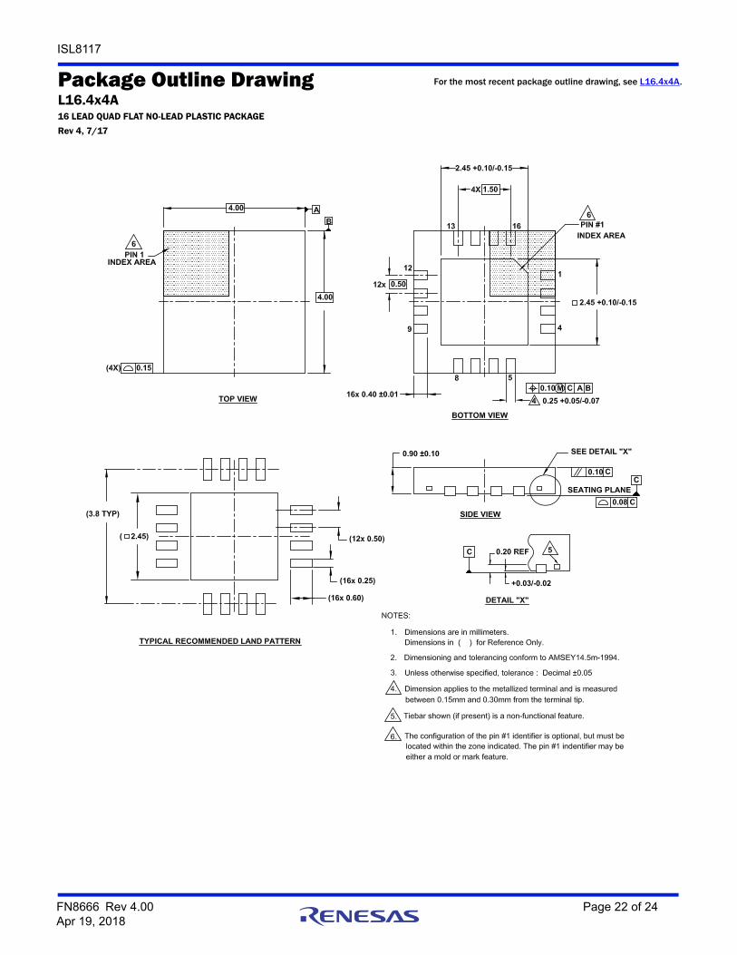
FN8666 Rev 4.00 Page 22 of 24Apr 19, 2018
Package Outline DrawingL16.4x4A16 LEAD QUAD FLAT NO-LEAD PLASTIC PACKAGE
Rev 4, 7/17
For the most recent package outline drawing, see L16.4x4A.

ISL8117
FN8666 Rev 4.00 Page 23 of 24Apr 19, 2018
Package Outline DrawingM16.173A16 LEAD HEATSINK THIN SHRINK SMALL OUTLINE PACKAGE (HTSSOP)
Rev 1, 2/15
0.09 TO 0.20
SEE DETAIL "X"
DETAIL "X"
TYPICAL RECOMMENDED LAND PATTERN
TOP VIEW
SIDE VIEW
END VIEW
Dimension does not include mold flash, protrusions or gate burrs.Mold flash, protrusions or gate burrs shall not exceed 0.15 per side.
Dimension does not include interlead flash or protrusion. Interlead flash or protrusion shall not exceed 0.25 per side.
Dimensions are measured at datum plane H.
Dimensioning and tolerancing per ASME Y14.5M-1994.
Dimension does not include dambar protrusion. Allowable protrusion shall be 0.08mm total in excess of dimension at maximum material
condition. Minimum space between protrusion and adjacent lead is 0.07mm.
Dimension in ( ) are for reference only.
Conforms to JEDEC MO-153.
6.
3.
5.
4.
2.
1.
NOTES:
7.
(0.65 TYP)
(5.65)
(0.35 TYP)
0.90 +0.15/-0.10
0.60 ±0.150.15 MAX
0.05 MIN
PLANEGAUGE
0.25
1.00 REF
(1.45)
16
2
1
3
8
B
1 3
9
A
PIN #1I.D. MARK
5.00 ±0.10
6.40
4.40 ±0.10
0.65
1.20 MAX
0.25 +0.05/-0.06 5
C
H
0.20 C B A
0.10 C
- 0.05
0.10 C B AM
3.00 ±0.10
3.00 ±0.10
EXPOSED THERMAL PAD
BOTTOM VIEW
SEATINGPLANE
0°-8°
( 3.00)
For the most recent package outline drawing, see M16.173A.

http://www.renesas.comRefer to "http://www.renesas.com/" for the latest and detailed information.
Renesas Electronics America Inc.1001 Murphy Ranch Road, Milpitas, CA 95035, U.S.A.Tel: +1-408-432-8888, Fax: +1-408-434-5351Renesas Electronics Canada Limited9251 Yonge Street, Suite 8309 Richmond Hill, Ontario Canada L4C 9T3Tel: +1-905-237-2004Renesas Electronics Europe LimitedDukes Meadow, Millboard Road, Bourne End, Buckinghamshire, SL8 5FH, U.KTel: +44-1628-651-700, Fax: +44-1628-651-804Renesas Electronics Europe GmbHArcadiastrasse 10, 40472 Düsseldorf, Germany Tel: +49-211-6503-0, Fax: +49-211-6503-1327Renesas Electronics (China) Co., Ltd.Room 1709 Quantum Plaza, No.27 ZhichunLu, Haidian District, Beijing, 100191 P. R. ChinaTel: +86-10-8235-1155, Fax: +86-10-8235-7679Renesas Electronics (Shanghai) Co., Ltd.Unit 301, Tower A, Central Towers, 555 Langao Road, Putuo District, Shanghai, 200333 P. R. China Tel: +86-21-2226-0888, Fax: +86-21-2226-0999Renesas Electronics Hong Kong LimitedUnit 1601-1611, 16/F., Tower 2, Grand Century Place, 193 Prince Edward Road West, Mongkok, Kowloon, Hong KongTel: +852-2265-6688, Fax: +852 2886-9022Renesas Electronics Taiwan Co., Ltd.13F, No. 363, Fu Shing North Road, Taipei 10543, TaiwanTel: +886-2-8175-9600, Fax: +886 2-8175-9670Renesas Electronics Singapore Pte. Ltd.80 Bendemeer Road, Unit #06-02 Hyflux Innovation Centre, Singapore 339949Tel: +65-6213-0200, Fax: +65-6213-0300Renesas Electronics Malaysia Sdn.Bhd.Unit 1207, Block B, Menara Amcorp, Amcorp Trade Centre, No. 18, Jln Persiaran Barat, 46050 Petaling Jaya, Selangor Darul Ehsan, MalaysiaTel: +60-3-7955-9390, Fax: +60-3-7955-9510Renesas Electronics India Pvt. Ltd.No.777C, 100 Feet Road, HAL 2nd Stage, Indiranagar, Bangalore 560 038, IndiaTel: +91-80-67208700, Fax: +91-80-67208777Renesas Electronics Korea Co., Ltd.17F, KAMCO Yangjae Tower, 262, Gangnam-daero, Gangnam-gu, Seoul, 06265 KoreaTel: +82-2-558-3737, Fax: +82-2-558-5338
SALES OFFICES
© 2018 Renesas Electronics Corporation. All rights reserved.Colophon 7.0
(Rev.4.0-1 November 2017)
Notice
1. Descriptions of circuits, software and other related information in this document are provided only to illustrate the operation of semiconductor products and application examples. You are fully responsible for
the incorporation or any other use of the circuits, software, and information in the design of your product or system. Renesas Electronics disclaims any and all liability for any losses and damages incurred by
you or third parties arising from the use of these circuits, software, or information.
2. Renesas Electronics hereby expressly disclaims any warranties against and liability for infringement or any other claims involving patents, copyrights, or other intellectual property rights of third parties, by or
arising from the use of Renesas Electronics products or technical information described in this document, including but not limited to, the product data, drawings, charts, programs, algorithms, and application
examples.
3. No license, express, implied or otherwise, is granted hereby under any patents, copyrights or other intellectual property rights of Renesas Electronics or others.
4. You shall not alter, modify, copy, or reverse engineer any Renesas Electronics product, whether in whole or in part. Renesas Electronics disclaims any and all liability for any losses or damages incurred by
you or third parties arising from such alteration, modification, copying or reverse engineering.
5. Renesas Electronics products are classified according to the following two quality grades: “Standard” and “High Quality”. The intended applications for each Renesas Electronics product depends on the
product’s quality grade, as indicated below.
"Standard": Computers; office equipment; communications equipment; test and measurement equipment; audio and visual equipment; home electronic appliances; machine tools; personal electronic
equipment; industrial robots; etc.
"High Quality": Transportation equipment (automobiles, trains, ships, etc.); traffic control (traffic lights); large-scale communication equipment; key financial terminal systems; safety control equipment; etc.
Unless expressly designated as a high reliability product or a product for harsh environments in a Renesas Electronics data sheet or other Renesas Electronics document, Renesas Electronics products are
not intended or authorized for use in products or systems that may pose a direct threat to human life or bodily injury (artificial life support devices or systems; surgical implantations; etc.), or may cause
serious property damage (space system; undersea repeaters; nuclear power control systems; aircraft control systems; key plant systems; military equipment; etc.). Renesas Electronics disclaims any and all
liability for any damages or losses incurred by you or any third parties arising from the use of any Renesas Electronics product that is inconsistent with any Renesas Electronics data sheet, user’s manual or
other Renesas Electronics document.
6. When using Renesas Electronics products, refer to the latest product information (data sheets, user’s manuals, application notes, “General Notes for Handling and Using Semiconductor Devices” in the
reliability handbook, etc.), and ensure that usage conditions are within the ranges specified by Renesas Electronics with respect to maximum ratings, operating power supply voltage range, heat dissipation
characteristics, installation, etc. Renesas Electronics disclaims any and all liability for any malfunctions, failure or accident arising out of the use of Renesas Electronics products outside of such specified
ranges.
7. Although Renesas Electronics endeavors to improve the quality and reliability of Renesas Electronics products, semiconductor products have specific characteristics, such as the occurrence of failure at a
certain rate and malfunctions under certain use conditions. Unless designated as a high reliability product or a product for harsh environments in a Renesas Electronics data sheet or other Renesas
Electronics document, Renesas Electronics products are not subject to radiation resistance design. You are responsible for implementing safety measures to guard against the possibility of bodily injury, injury
or damage caused by fire, and/or danger to the public in the event of a failure or malfunction of Renesas Electronics products, such as safety design for hardware and software, including but not limited to
redundancy, fire control and malfunction prevention, appropriate treatment for aging degradation or any other appropriate measures. Because the evaluation of microcomputer software alone is very difficult
and impractical, you are responsible for evaluating the safety of the final products or systems manufactured by you.
8. Please contact a Renesas Electronics sales office for details as to environmental matters such as the environmental compatibility of each Renesas Electronics product. You are responsible for carefully and
sufficiently investigating applicable laws and regulations that regulate the inclusion or use of controlled substances, including without limitation, the EU RoHS Directive, and using Renesas Electronics
products in compliance with all these applicable laws and regulations. Renesas Electronics disclaims any and all liability for damages or losses occurring as a result of your noncompliance with applicable
laws and regulations.
9. Renesas Electronics products and technologies shall not be used for or incorporated into any products or systems whose manufacture, use, or sale is prohibited under any applicable domestic or foreign laws
or regulations. You shall comply with any applicable export control laws and regulations promulgated and administered by the governments of any countries asserting jurisdiction over the parties or
transactions.
10. It is the responsibility of the buyer or distributor of Renesas Electronics products, or any other party who distributes, disposes of, or otherwise sells or transfers the product to a third party, to notify such third
party in advance of the contents and conditions set forth in this document.
11. This document shall not be reprinted, reproduced or duplicated in any form, in whole or in part, without prior written consent of Renesas Electronics.
12. Please contact a Renesas Electronics sales office if you have any questions regarding the information contained in this document or Renesas Electronics products.
(Note 1) “Renesas Electronics” as used in this document means Renesas Electronics Corporation and also includes its directly or indirectly controlled subsidiaries.
(Note 2) “Renesas Electronics product(s)” means any product developed or manufactured by or for Renesas Electronics.