isolated hydrogen in ii{vi zinc{chalcogenide widegap .../cite> · modelo
TRANSCRIPT

Rui Cesar Vilao
Isolated hydrogen
in II–VI zinc–chalcogenide
widegap semiconductors
modelled by the muon analogue
Faculdade de Ciencias e Tecnologia
Universidade de Coimbra
Coimbra – 2007

ii

Rui Cesar Vilao
Isolated hydrogen in II–VI zinc–chalcogenidewidegap semiconductors modelled by the muon
analogue
[Hidrogenio isolado em calcogenos de zinco da famılia
II-VI com propriedades semicondutoras e intervalo
largo de energias proibidas, estudado atraves da
analogia com o muao]
Dissertacao de doutoramento em Fısica,
especialidade de Fısica Experimental,
submetida a Faculdade de Ciencias e Tecnologia,
Universidade de Coimbra
Coimbra - 2007

iv

Aos meus Pais
A Susana

vi
Abstract
We have investigated the behaviour of isolated hydrogen in II–VI zinc chalco-
genide widegap semiconductors, by means of the positive-muon analogue. A broad
program of muon-spin rotation, relaxation and resonance measurements was under-
taken for monocrystalline samples of ZnSe, upon adequate characterization (parti-
cularly on the electrical transport properties, by means of Hall-effect and resistivity
measurements). Two compact paramagnetic muonium states MuI and MuII were
identified and the interconversion process was characterized. Capture of a second
electron by MuII, forming the negative ion Mu−II was observed as well. This charged
state becomes thermally unstable above 60 K and we relate this to possible ioni-
zation to the conduction band and estimate the corresponding acceptor level. In
adition to ZnSe, monocrystalline samples of ZnS and ZnTe were investigated. Only
one paramagnetic state is observed in ZnS, whose behaviour is shown to be much
similar to that of MuII in ZnSe. In ZnTe, only a diamagnetic state is observed,
which we suggest corresponds to a deep donor in this material. Finally, a global
configuration and energy level model is presented for muonium/hydrogen in II–VI
semiconductors.

viii

Resumo
Neste trabalho investigou-se o comportamento, atraves da analogia com o muao
positivo, do hidrogenio isolado em materiais calcogenos de zinco com propriedades
semicondutoras e intervalo largo de energias proibidas, da famılia II-VI. Foi rea-
lizado um programa amplo de medidas experimentais de rotacao, relaxacao e res-
sonancia do spin do muao em amostras monocristalinas de ZnSe devidamente car-
acterizadas (particularmente do ponto de vista das propriedades de transporte
electrico, atraves de medidas de efeito de Hall e resistividade electrica). Identificou-
se dois estados paramagneticos compactos de muonio, MuI e MuII, e caracterizou-se
o processo de interconversao. Observou-se ainda a captura de um segundo electrao
pelo estado MuII, formando o iao negativo Mu−II. Este estado negativamente car-
regado e instavel para temperaturas superiores a 60 K, possivelmente ionizando
para a banda de conducao, tendo sido determinado o presumıvel nıvel aceitador
correspondente. Para alem de ZnSe, investigou-se tambem amostras monocristali-
nas de ZnS e ZnTe. Observa-se apenas um estado de muonio paramagnetico em
ZnS, cujo comportamento se verificou ser muito semelhante ao do estado MuII
existente em ZnSe. Em ZnTe observa-se um estado diamagnetico que sugerimos
corresponder a um dador profundo neste material. Finalmente, apresenta-se um
modelo global para as configuracoes e nıveis de energia do muonio/hidrogenio nos
semiconductores da famılia II-VI.

x
Acknowledgements
A work such as the one now presented is necessarily a team work. The input
and collaboration of many people is present at all stages, from the initial ideas
and proposals, through the beamline days and discussion at all levels of the ex-
perimental data and respective significance, up to the final redaction. It is to me
a privilege to make part of a team such as the one which helped to complete this
work. A scientific privilege, certainly, but a personal privilege as well. I am very
happy to express now my public thanks:
- to Prof. Dr. Joao Campos Gil, whom I owe a most dedicated, friendly, present
guidance, in the big lines as in the little details.
- to Prof. Dr. Nuno Ayres de Campos, whose counsel, encouragement and
friendship helped me looking farther with confidence.
- to Prof. Dr. Alois Weidinger, whose profound physical insight, shared friendly
and patiently in intense interaction and discussions, brought me immense benefits.
- to Dr. Helena Vieira Alberto, a quotidian source of science, humanism and
friendship.
- to Joao Pedro Duarte, comrade of many scientific and non-scientific fights,
always fought with wit and joy.
- to Prof. Dr. Stephen Cox, Prof. Dr. Roger Lichti and Dr. Kim Chow, who
have contributed to this investigation with their eminent knowledge, as well as
with many days of hard work.
I would also like to gratefully acknowledge the kind help, during this work, of
Dr. Benilde Costa, Dr. Francisco Gil, Dr. D. Siche, Dr. K. Irmscher, Marco
Peres, Prof. Dr. Teresa Monteiro, Prof. Dr. Ermelinda Eusebio, Dr. Manuela
Silva, Victor Hugo Rodrigues, Prof. Dr. Jose Antonio Paixao, Dr. Ana Maria
Matos Beja, Dr. Bassam Hitti, Dr. Stephen Cottrell, Dr. James Lord, Dr. U.
Zimmermann, Dr. Robert Scheuermann, Dr. Alex Amato, Dr. Hubertus Luetkens,
Dr. Dierk Herlach, Dr. Philip King, as well of my colleagues at the Physics
Department of the University of Coimbra.

xii

Contents
1 Hydrogen in semiconductors 1
1.1 Introduction . . . . . . . . . . . . . . . . . . . . . . . . . . . . . . . 1
1.2 Hydrogen as a passivating/activating impurity . . . . . . . . . . . . 2
1.3 Isolated hydrogen in semiconductors . . . . . . . . . . . . . . . . . 3
1.3.1 Hydrogen as a compensating amphoteric centre . . . . . . . 4
1.3.2 Hydrogen as a source of conductivity . . . . . . . . . . . . . 8
1.4 Isolated hydrogen in zinc II-VI compounds . . . . . . . . . . . . . . 9
1.4.1 Zinc II-VI compound semiconductors for optoelectronics . . 9
1.4.2 Hydrogen in zinc chalcogenides . . . . . . . . . . . . . . . . 13
2 The µSR techniques 19
2.1 Introduction . . . . . . . . . . . . . . . . . . . . . . . . . . . . . . . 19
2.2 µ+ as a light pseudo-isotope of hydrogen . . . . . . . . . . . . . . . 20
2.3 Muonium . . . . . . . . . . . . . . . . . . . . . . . . . . . . . . . . 22
2.3.1 Preliminary remarks . . . . . . . . . . . . . . . . . . . . . . 22
2.3.2 Hyperfine structure of the muonium atom . . . . . . . . . . 24
2.3.3 Muonium dynamics . . . . . . . . . . . . . . . . . . . . . . . 37
2.4 Production of polarized muon beams . . . . . . . . . . . . . . . . . 42
2.4.1 Muon decay . . . . . . . . . . . . . . . . . . . . . . . . . . . 42
2.4.2 Polarized muon beams . . . . . . . . . . . . . . . . . . . . . 45
2.5 Muon implantation and thermalization . . . . . . . . . . . . . . . . 46
2.6 Muon spin rotation, relaxation, resonance . . . . . . . . . . . . . . 51
2.6.1 Basic experimental setup . . . . . . . . . . . . . . . . . . . . 51
xiii
xiv CONTENTS
2.6.2 Muon spin rotation . . . . . . . . . . . . . . . . . . . . . . . 55
2.6.3 Muon spin relaxation . . . . . . . . . . . . . . . . . . . . . . 58
2.6.4 Muon spin resonance . . . . . . . . . . . . . . . . . . . . . . 59
2.6.5 User facilities and spectrometers . . . . . . . . . . . . . . . . 66
3 Sample characterization 71
3.1 Introduction . . . . . . . . . . . . . . . . . . . . . . . . . . . . . . . 71
3.2 Samples . . . . . . . . . . . . . . . . . . . . . . . . . . . . . . . . . 72
3.2.1 ZnSe . . . . . . . . . . . . . . . . . . . . . . . . . . . . . . . 72
3.2.2 ZnS and ZnTe . . . . . . . . . . . . . . . . . . . . . . . . . . 82
3.3 Resistivity and Hall effect in ZnSe . . . . . . . . . . . . . . . . . . . 83
3.3.1 Ohmic contacts . . . . . . . . . . . . . . . . . . . . . . . . . 83
3.3.2 Ohmic contacts to ZnSe . . . . . . . . . . . . . . . . . . . . 87
3.3.3 Resistivity and Hall effect measurements . . . . . . . . . . . 91
3.3.4 Results . . . . . . . . . . . . . . . . . . . . . . . . . . . . . . 101
4 Experimental results and discussion I: ZnSe 105
4.1 Introduction . . . . . . . . . . . . . . . . . . . . . . . . . . . . . . . 105
4.2 High-transverse field spectroscopy . . . . . . . . . . . . . . . . . . . 107
4.2.1 Novel deep muonium center in ZnSe . . . . . . . . . . . . . . 107
4.2.2 Temperature dependence of the paramagnetic states: AA
sample . . . . . . . . . . . . . . . . . . . . . . . . . . . . . . 110
4.2.3 Temperature dependence of the paramagnetic states: Ctec
sample . . . . . . . . . . . . . . . . . . . . . . . . . . . . . . 119
4.2.4 Discussion . . . . . . . . . . . . . . . . . . . . . . . . . . . . 122
4.3 Low-transverse field spectroscopy . . . . . . . . . . . . . . . . . . . 124
4.3.1 AA sample . . . . . . . . . . . . . . . . . . . . . . . . . . . . 124
4.3.2 Ctec sample . . . . . . . . . . . . . . . . . . . . . . . . . . . 128
4.4 Final-state analysis experiments . . . . . . . . . . . . . . . . . . . . 135
4.4.1 Discussion . . . . . . . . . . . . . . . . . . . . . . . . . . . . 138
4.5 Further experimental information . . . . . . . . . . . . . . . . . . . 148
4.5.1 Probing Mu dynamics with LF . . . . . . . . . . . . . . . . 148

CONTENTS xv
4.5.2 Development of doping-dependent studies . . . . . . . . . . 152
4.5.3 High temperature investigations . . . . . . . . . . . . . . . . 155
4.6 Conclusive remarks . . . . . . . . . . . . . . . . . . . . . . . . . . . 161
5 Experimental results and discussion II: ZnS and ZnTe 163
5.1 ZnS . . . . . . . . . . . . . . . . . . . . . . . . . . . . . . . . . . . 164
5.1.1 High transverse field spectroscopy . . . . . . . . . . . . . . . 164
5.1.2 Low transverse field spectroscopy . . . . . . . . . . . . . . . 168
5.1.3 Final-state analysis of the diamagnetic fraction . . . . . . . 171
5.1.4 Probing Mu dynamics with LF . . . . . . . . . . . . . . . . 173
5.2 ZnTe . . . . . . . . . . . . . . . . . . . . . . . . . . . . . . . . . . . 174
5.2.1 Spectroscopic measurements . . . . . . . . . . . . . . . . . . 174
5.2.2 Final-state analysis of the diamagnetic fraction . . . . . . . 178
5.2.3 High-temperature spectroscopic incursion . . . . . . . . . . . 182
5.2.4 Probing Mu dynamics with LF . . . . . . . . . . . . . . . . 184
5.3 Conclusive remarks . . . . . . . . . . . . . . . . . . . . . . . . . . . 186
6 Conclusions and perspectives 187
6.1 Towards a final synthesis . . . . . . . . . . . . . . . . . . . . . . . . 187
6.1.1 Configuration model . . . . . . . . . . . . . . . . . . . . . . 188
6.1.2 Energy levels . . . . . . . . . . . . . . . . . . . . . . . . . . 190
6.2 Future developments . . . . . . . . . . . . . . . . . . . . . . . . . . 192
6.2.1 Open questions . . . . . . . . . . . . . . . . . . . . . . . . . 193
6.2.2 Related investigations . . . . . . . . . . . . . . . . . . . . . 195
Appendix A 199
Bibliography 201

xvi CONTENTS

Chapter 1
Hydrogen in semiconductors
Embarque vossa docura
que ca nos entenderemos...
Tomareis um par de remos,
veremos como remais;
e, chegando ao nosso cais,
nos vos desembarcaremos.1
Gil Vicente
Auto da Barca do Inferno
1.1 Introduction
Impurities play an essential part in the physics of semiconductors. The extreme
sensibility of the electrical and optical properties of the members of this class of
materials with respect to the presence of impurity atoms may be regarded as one
of its most defining characteristics [See82, Yu99]. Hydrogen occupies a special
role among all impurities. As the simplest atom, one might expect hydrogen to
have a specially simple behaviour in semiconductors, upon which generalizations to
other impurities could be inferred. Notwithstanding the current state of hydrogen
research in semiconductors depicts an extremely complex impurity which assumes
a variety of forms, from several possible atomic configurations to molecular states
1Free translation: ”Climb your sweetness aboard and we shall go along... You shall take a pair
of oars, we shall watch you rowing; and, when we arrive to our pier, we shall step you off.”

2 CHAPTER 1. HYDROGEN IN SEMICONDUCTORS
and complexation with other impurities and defects [Est95, Mye92, Nic98, Nic99a,
Pan91, Pea94, VdW05, VdW06]. Much interest is deposited in the knowledge of
the hydrogen impurity per se, due to its omnipresence in semiconducting materials
science.
This interest extends also strongly to several technological applications of semi-
conductors. Hydrogen atoms are present either in the materials’s growth, as part
of the source materials or carrier gases, or in the processing itself. This pervasive-
ness urges the understanding of the consequences of hydrogen incorporation in the
materials.
In this chapter we intend to concisely place the research directly associated with
this work inside that broader context. After an inevitably very brief introduction
to the hydrogen in semiconductors subject we bring into special prominence the
contribution put forward by the muon spin techniques, characteristic of this work,
to the study of isolated hydrogen in semiconductors. Reasons for the choice of
II-VI semiconductors for the theme os this work are presented and are followed by
an outline of the present state of the art of the research on isolated hydrogen in
this class of semiconductors.
1.2 Hydrogen as a passivating/activating impu-
rity
Hydrogen is extremely reactive inside materials, and is best known for its role in the
passivation of defects or impurities in semiconductors, thus altering significatively
its electrical and optical properties.
One of the most significant effects of hydrogen incorporation in semiconductor’s
properties (and also one of the examples known for a longer time) is the passiva-
tion of dangling bonds in amorphous silicon [Pan78, Pau76]. This passivation
phenomenon removes the unwanted electron energy levels from the bandgap, thus
increasing the carriers mobility and allowing amorphous-silicon-based technology
such as solar cells or thin-film transistors [Nic99b].
Hydrogen was also found to activate impurities in semiconductors, namely the

1.3. ISOLATED HYDROGEN IN SEMICONDUCTORS 3
formation of shallow-acceptor Si–H and C–H complexes in Ge, the isoelectronic Si
and C impurities being otherwise electrically inactive [Hal80]. However, this effect
is far less common than passivation.
The passivation of impurities is also known since the 1980’s, when the boron
acceptor in Si was found to be deactivated by hydrogen [Pan83, Sah83]. Since
then, many more examples were found not only in the elemental semiconductors,
but also in compound semiconductors, namely from the III–V and II–VI families.
Detailed acounts up to 2003 can be found in a number of reviews [Est95, Mye92,
Myn03, Nic98, Nic99a, Pan91, Pea94].
Among recent developments, hydrogen was found to passivate Mn acceptors
in ferromagnetic GaMnAs, changing epilayers from metallic to semiconducting be-
haviour upon hydrogenation [Bra04].
It is important to stress the distinction between passivation and compensation:
passivation implies the formation of a complex between two impurities/defects,
thereby forming a new defect with electrical and optical properties distinct from the
two originating defects. In compensation, the two defects keep their individuality
and mutually cancel the respective contributions to the conductivity. In terms of
electrical transport characteristics, the two situations may be distinguished by the
charge–carrier mobilities, which are smaller in the case of compensation [VdW05].
Despite the importance of the passivation effects, the hydrogen impurity per
se may also affect the host material properties, and much research effort has been
dedicated in the past decades to clarify the role of isolated hydrogen.
1.3 Isolated hydrogen in semiconductors
Due to the high reactivity of hydrogen, the studies on isolated hydrogen are much
more demanding for usual experimental techniques. The information obtained by
experimental methods that are sensible to hydrogen itself is therefore much scarcer,
usually painfully obtained, and limited to a reduced number of systems, notably
silicon [Bon99, Bon02, Her01, Hit99] and, recently, zinc oxide [Cox01a, Hof02,
Lav02, McC02]. In the last thirty years, the use of positive muons as a model for

4 CHAPTER 1. HYDROGEN IN SEMICONDUCTORS
protons, together with theoretical work, has immensely enlarged the perspectives
in this relevant, albeit hard, field. We shall here concisely present some essential
results of these investigations, which are essential guides in the work now presented:
from the ”usual” role of hydrogen as a compensating center and the vast amount
of information for hydrogen in silicon, to the possibility that hydrogen be a source
of conductivity in ZnO and other ionic semiconductors. The information obtained
by the muon analogue has played a major part in these investigations.
1.3.1 Hydrogen as a compensating amphoteric centre
Silicon is the system where most intensive resarch on isolated hydrogen has been
done. Two charged states have been identified: H− at the interstitial tetrahe-
dral position and H+ at the bond-centre site, together with the respective neutrals
[Hit99]. Unlike the tetrahedral site, the bond-centre position was completely un-
expected: the associated neutral was first seen in µSR measurements [Bre73], and
labelled ”anomalous muonium”, in contrast with the tetrahedral ”normal muo-
nium”. The identification at the bond-centre site was proposed on the basis of
chemical arguments [Cox86, Sym84] and confirmed by µSR [Kie88]. This cen-
tre was also seen in 1H-EPR [Gor87] and by deep–level transient spectroscopy2,
in implanted proton experiments [Bon99], which confirmed the site and electronic
structure assigned by µSR. The bond-centre neutral state is found to be more stable
than the tetrahedral neutral state [Est95]. Muonium thus represents an example
of interstitial metastability, i.e. coexistence of two distinct atomic arrangements
for a single charge state of a defect [Bar85, Est87].
This system has now been exhaustively scrutinized by a number of experimental
methods:
(i) after twenty years of investigations on dozens of samples from extreme p–
2The DLTS method, basically, relies on the dependence of the width, therefore of the capaci-
tance, of the depletion layer in a junction diode with the doping concentrations. The injection of
a short pulse in the forward direction injects carriers in the junction and floods the deep traps,
changing the capacitance. The return to equilibrium is afterwards observed as the time evolution
of the junction voltage. Cf. [See82], p. 129.

1.3. ISOLATED HYDROGEN IN SEMICONDUCTORS 5
type to extreme n–type, a detailed model of the muonium states and dynamics in
silicon has been put forward [Hit99], including the determination of the muonium
levels in the bandgap: the Mu(0/+) donor level was placed 0.21 eV below the
conduction band minimum and the Mu(-/0) acceptor level was estimated to lie
approximately at 0.56 eV below the conduction band minimum;
(ii) the experimental investigations with protons have progressed much more
slowly, due to the difficulties of observing isolated hydrogen and have followed two
distinct paths: either using implanted protons [Bon99, Bon02] or finding ways to
dissociate hydrogen–containing complexes and subsequently observing its behav-
iour [Her01]. The results from the latter method have the advantage of being free
from the radiolysis problematics affecting both µSR and the techniques based on
implanted protons.
The positions of the (bond-centre) donor (0/+) and (tetrahedral) acceptor (-/0)
energy levels below the bottom of the conduction band, for isolated hydrogen in
silicon, are summarized in table 1.1. The µSR slight differences are expected from
differences in the proton and muon zero point motion. Similar differences, both
in magnitude and trend, have been found from path-integral molecular dynamics
simulations for hydrogen/muonium in diamond [Her06].
Method E(0/+) E(-/0)
Muon implantation 0.21 eV [Kre95] < 0.56 eV [Hit99]
Proton implantation 0.16 eV [Hol91] 0.65 eV [Bon02]
Dissociation of P-H complexes [Her01] 0.16 eV 0.67 eV
First-principles calculations [VdW89] 0.2 eV 0.6 eV
Table 1.1: Position of the (isolated) hydrogen donor (0/+) and acceptor (-/0)
energy conversion level below the bottom of the conduction band, as determined
by several experimental methods and by first-principles calculations.

6 CHAPTER 1. HYDROGEN IN SEMICONDUCTORS
These results, together with the associated theoretical work [Her01], allow a
rather complete view on the fundamental characteristics of isolated hydrogen in
silicon. An essential characteristic is that the acceptor level −/0, corresponding
to the ionization of the doubly charged state H−, is lower in the bandgap than
the donor level 0/+ (cf. Fig. 1.1). This apparently paradoxical result of the
larger binding energy of the second electron, despite Coulombic repulsion effects,
is explained attending to the implied change in configuration: BC for H+ and T
for H−. The energy change associated with the lattice relaxation in the different
configurations explains this otherwise odd behaviour [And75, Wei82].
The Anderson U = E(0/−)−E(+/0) quantity, defined as the difference between
the energy of the 0/− level, E(0/−) and the energy of the +/0 level, E(+/0), is
therefore negative. The shortened expression negative-U is then frequently used to
express this inverted ordering of the donor and acceptor level in the bandgap. In
the positive-U or normal ordering, the energy required to ionize an electron from
the singly occupied state is larger than that required to ionize an electron from the
doubly occupied state, and therefore the donor level 0/+ lies lower in the bandgap
than the acceptor level −/0.
Another consequence from the negative-U situation is that, in thermodynamical
equilibrium, the neutral states are not stable, their formation energies being always
higher than one of the charged states. Depending on the position of the Fermi
level in the bandgap, the formation energies of the neutral states H0BC and H0
T
are either higher than the formation energy of H+BC (for Fermi levels in the lower
midgap), or higher than the formation energy of H−T (for Fermi levels in the upper
midgap). This means that if the material is electron-defficient (p-type), hydrogen
will tend to donate its electron to the conduction band, forming the H+BC species
and consequently acting as a donor. If the material is electron rich (n-type),
hydrogen will tend to capture and extra electron from the conduction band, forming
the H−T species, and therefore behaving as an acceptor. In short, hydrogen will
tend to always counteract the prevailing conductivity, and to act as an amphoteric
impurity.
It should also be pointed that, at some value of the Fermi level in the bandgap,

1.3. ISOLATED HYDROGEN IN SEMICONDUCTORS 7
the formation energies of the H+BC configuration and the H−
T configuration are
found to be equal. This defines a transition level, loosely designated E(+/−),
which is particularly popular among theorists, because it corresponds to a tran-
sition between ground state configurations, which are easily accessible via total
energy calculations with conventional methods. Theoretical works therefore tend
to overlook the experimentally accessible neutral states and the corresponding
transition levels, by concentrating in the +/− transition level and, at most, at
the lowest formation energy neutral state. Also, it is even more difficult to ad-
dress theoretically the metastability issue of the neutral species, which is never-
theless established experimentally in firm grounds for Si and other semiconductors
[Bon02, Bon03, Est87, Hol91]. These difficulties do not facilitate the comparison
of experimental information with theoretical calculations.
The amphoteric behaviour of hydrogen is not exclusive of Si, but is common to
other technologically important semiconductors. Evidence for this, both theoretical
and experimental, have been accumulated for Ge [Bud00, Dob04], diamond, GaAs
[Lic03] and GaN [Neu95].
-/0 0/+
Fermi level (eV)
Form
ation e
nerg
y (
eV
)
+/-
Figure 1.1: Formation energies of interstitial H+BC , H0
BC and H−T in silicon, as a
function of the position of the Fermi level in the bandgap [Her01]. The neutral
state is never stable, for any position of the Fermi level, implying that the acceptor
level −/0 lies lower than the donor level 0/+. In this negative-U situation, the
conversion level +/− plays an important role in the theoretical conjectures.

8 CHAPTER 1. HYDROGEN IN SEMICONDUCTORS
1.3.2 Hydrogen as a source of conductivity
Amphoteric behaviour of hydrogen in semiconductors is, as pointed above, com-
mon to many of the most technologically relevant semiconductors. It implies that
isolated hydrogen acts as a compensating centre, and not as an electrically active
impurity.
The possibility that hydrogen behaved as a source of conductivity in materials
had been raised as early as 1954 by E. Mollwo [Hei59, Mol54], who observed signifi-
cant changes in the conductivity and luminescence of ZnO crystals upon heating in
hydrogen atmosphere at high temperatures (above 500 oC). However, this subject
only reappeared in 1999, with the discovery of a muonium state in CdS with a very
small hyperfine interaction and an ionization energy of 26 meV [Gil99]. Parallel
theoretical work predicted that hydrogen behaved as a shallow donor in ZnO as
well [VdW00]. This prompted the finding in ZnO [Cox01a] of a muonium state
similar to that found in CdS and the other cadmium chalcogenides CdSe and CdTe
[Gil01].
This field has since then known intensive developments in many fronts:
(i) the shallow donor state in ZnO has been thoroughly scrutinized by many
experimental methods and has been confirmed by EPR/ENDOR [Hof02] and IR
measurements [Lav02, McC02].
(ii) µSR investigations in ZnO and the cadmium chalcogens have characterized
exhaustively the shallow-donor muonium states [Alb01, Cox01a, Cox01b, Cox03b,
Gil99, Gil00, Gil01] and suggested its location at an antibonding site [Gil01, Shi02].
The extended atomic orbital characteristic of the shallow donor wavefunction has
also been investigated by probing the electron interaction with the nearest nuclei
[Lor01]. Measurement of the g-value of the muonium electron were done and the
results are consistent with known g-values for conduction electrons, which is a
strong support for the shallow-donor model [Lor04]; this has prompted further
technical developments in order to determine experimentally the sign of the g-
factor as well [Lor06]. Experiments in p- and n-type CdTe have addressed the role
of the interaction of the muonium states with impurities, and revealed the same
electronic structure for the muonium centers, albeit with significantly different

1.4. ISOLATED HYDROGEN IN ZINC II-VI COMPOUNDS 9
formation probabilities [Cor04].
(iii) similar muonium states have been found or proposed in oxides (BaO, CdO,
CeO2, HfO2, SnO2, TiO2, WO3, Y2O3, ZrO2) [Cox06a, Cox06b], nitrides [Dav03,
Shi04] and chalcopyrites [Vil03b]. Such developments have been prompted by
theoretical calculations suggesting that the +/− conversion level might be located
at a fixed value in an absolute energy scale [Kil02, Rob03, VdW03], for a wide
range of semiconductors.
(iv) hydrogen-induced surface conductivity effects were also found in diamond
[Mai00, Str04], and in ZnO [Wan05].
1.4 Isolated hydrogen in zinc II-VI compounds
1.4.1 Zinc II-VI compound semiconductors for optoelec-
tronics
The zinc chalcogenides have been considered for long as potential candidates for
use in optoelectronics applications in the blue/green region. However, progress was
hampered by the common tendency of these materials (and of II–VI semiconductors
in general) to unipolarity: ZnSe and ZnS are usually n–type and resist to p–type
doping, and the inverse happens with ZnTe [Cha94, Des98, Zha02].
The interest in these materials, particularly in ZnSe, resurged in the 1990’s, with
the possibility of incorporating nitrogen acceptors above the equilibrium solubility,
by beam doping during molecular beam epitaxial growth [Ohk91, Par90]. This
allowed to produce reproducible p-type ZnSe films.
ZnSe has since then been thoroughly investigated, not only for the develop-
ment of laser applications in the blue-green region [Gun97], but also for infrared
optical applications [Gav03]. More recently, novel possible applications have been
considered, such as using it as the photoconductive medium for the generation
of terahertz radiation [Hol03, Kli05], or as the semiconductor layer in ferromag-
netic/semiconductor heterostructures for spintronics applications [Edd06]. ZnTe
has also appeared recently as a promising room-temperature ferromagnetic semi-

10 CHAPTER 1. HYDROGEN IN SEMICONDUCTORS
conductor, upon being doped with chromium [Oza06].
In the following paragraphs, we shall summarize the basic characteristics of
the zinc chalcogenides, with a special emphasis on the doping problem in these
materials.
Essential characteristics
The zinc chalcogenides ZnSe, ZnS and ZnTe all crystallize in the zinc blende struc-
ture3, which has the translational symmetry of the face-centered cubic lattice. The
conventional unit cell is depicted in Fig. 1.2. The most important interstitial posi-
tions can be seen there: the cation tetrahedral cage, surronded by four cations, the
corresponding anion tetrahedral cage, and the bonding positions - bond-center,
antibonding to the cation and antibonding to the anion. Some other positions
are sometimes considered in the literature, but the above mentioned are the most
important from both the theoretical and the experimental point of view.
The cation and anion cages are particularly important in the discussion of the
interstitial hydrogen in its various charged states. Its is commonly anticipated that
the negatively charged ion H− is stabilized in the positively-charged environment of
the cation cage and that the positively charged ion H+ prefers negatively charged
regions around the anion cage. Of course, this naıve view contains some heuristic
value, but is found to be broken easily for the positive species (a proton) in highly
covalent materials, where it easily forms chemical bonds within the material and
may become stable at unexpected sites such as the bond-centre. In ionic com-
pounds, it seems however that a more conventional location of H+ in the anion
cage is preferred, although the existence of chemical bonds with the anion may
mean that the respective location is closer to the antibonding site than the actual
center of the anion tetrahedron.
Table 1.2 summarizes the essential physical and electronical properties of these
compounds. ZnS, ZnS and ZnTe all present a direct bandgap, whose minimum
value in the reciprocal lattice is found at the Γ point in the centre of the Brillouin
3Actually, the prototypical compound of this crystallographical structure is ZnS, which is the
zinc blende.

1.4. ISOLATED HYDROGEN IN ZINC II-VI COMPOUNDS 11
BC
AB
T
T
AB
Figure 1.2: Conventional unit cell of the zinc blende structure: white circles in-
dicate the group-II cation and grey circles denote the group-VI anion. The most
important interstitial positions along the [111] direction are shown: bond-centre
(BC), anion tetrahedral (TVI), cation tetrahedral (TII), anion antibonding (ABVI)
and cation antibonding (ABII).

12 CHAPTER 1. HYDROGEN IN SEMICONDUCTORS
zone k=(0,0,0) [Ber87]. For ZnTe, the gap value corresponds to transition in the
green/blue region, and in ZnSe and ZnS these lie already in the ultraviolet zone.
Material a (A) Eg (eV) χ φ m0e/m0 m0
h/m0 ρ (g cm−3) ΘD (K)
ZnS 5.41 3.68 3.9 7.5 0.28 0.49 4.09 350
ZnSe 5.67 2.7 4.09∗ 6.82∗ 0.16 0.57 5.27 271
ZnTe 6.1 2.26 3.53∗ 5.76∗ 0.11 0.6 5.636
Table 1.2: Essential properties of the zinc chalcogenides : a - lattice parameter
at RT, Eg - bandgap at RT, χ - electron affinity, φ - photoelectric threshold (φ =
Eg+χ), m0e - electron effective mass at the bottom of the conduction band, m0
h - hole
effective mass at the top of the valence band, ρ - density, ΘD - Debye temperature.
All values were obtained in Ref. [Mad82], except those marked with * which are
from Ref. [Swa67].
The doping problem
As mentioned above, the zinc chalcogenides in particular and the II–VI materials
in general present a strong tendency to unipolarity, and usually are easily doped
in one of the types and resist being doped in the other type. ZnSe and ZnS are
usually n–type and hard to obtain p–type; ZnTe is usually p–type, but resists to
n–type doping [Cha94, Des98, Zha02].
A phenomenological ”doping limit rule” has been proposed to explain these
differences [Zha98], depending on the position of the valence band maximum and
the conduction band minimum with respect to vacuum and to pinning levels. In
this model, it is more probable not to achieve low-resistance p-type doping with a
deep valence band maximum (e.g. ZnSe and ZnS). Also, a higher conduction band
minimum turns it more difficult to obtain shallow donor levels (e.g. ZnTe).

1.4. ISOLATED HYDROGEN IN ZINC II-VI COMPOUNDS 13
A number of microscopic reasons have been raised to justify this behaviour. The
compensation by native defects is a popular topic, but it seems not to be enough
to justify the poor p–type doping in ZnSe [Lak91, Lak92], where the low solubility
of the dopant appears as a much more important factor [Neu89, VdW93b]. The
experimental success in achieving p–type doping in ZnSe has been obtained by
increasing the solubility of the dopant beyond its equilibrium value, in the already
mentioned N-doped MBE films [Ohk91, Par90]. Positive results have been achieved
as well in bulk ZnSe:Sb samples, by forming quasi-stable non–equilibrium states
via thermal treatments and subsequent quenching to RT [Pro02].
The passivation by formation of complexes with native defects and/or impuri-
ties seems to play an important role as well: the formation of DX centers hinders
n–type doping in ZnTe [Cha94]. In ZnSe, complexes of donors with zinc vacancies
have been reversibly formed by thermal annealing in different zinc atmospheres
and identified via EPR and positron annihilation [Geb02, Irm01, Pro00]; these
works clearly establish the possibility of controlling the conductivity of ZnSe by
this method.
1.4.2 Hydrogen in zinc chalcogenides
Complexes of hydrogen
Very little is known about the complexes of hydrogen in II–VI semiconductors
in general, and in the zinc chalcogenides in particular. Most of the information
concentrates on the nitrogen acceptor in ZnSe, whose interaction with hydrogen has
been thoroughly investigated, both experimentally [Ho95, Ho97, McC99, Tou00]
and theoretically [Tor03]. These investigations established the role of hydrogen in
the passivation of nitrogen in ZnSe:N. A similar role might be played regarding
other impurities in ZnSe, namely the As and P acceptors [McC99, Tor03].
More recently, post-growth H irradiation was found to passivate oxygen impu-
rity levels in ZnTe and Zn(Te,S), but not in Zn(Se,O) [Fel04, Pol04].
The research has also begun in ZnTe, where passivation of deep acceptors OTe
in bulk ZnTe [Bhu98, Bos99] and of nitrogen acceptors in MBE-grown ZnTe films

14 CHAPTER 1. HYDROGEN IN SEMICONDUCTORS
[Pel98] was found.
In the remainder II–VI’s, CdTe has received particular attention [McC99]. In
this compound, arsenic acceptors are found to be neutralized by hydrogen [Cle93].
Isolated hydrogen: terra incognita
The information about isolated hydrogen in the zinc chalcogenides up to now is even
more limited than that regarding hydrogen complexes. Up to now, only limited
exploratory work is available, both from theoretical and experimental point of view.
From the theoretical side, Kilic and Zunger refer having calculated [Kil03] the
equilibrium locations of H+, H0 and H− in the zinc chalcogenides to be the bond-
centre BC for the neutral and the positive species; the negative center prefers
the cation tetrahedral cage TZn. However, the detailed calculations have not been
published. These locations disagree with those presented by Van de Walle for ZnSe
[VdW02], who finds the cation antibonding site ABZn as the most stable for the
neutral and negative species. These results are summarized in Table 1.3.
Species Location [Kil03] Location [VdW02]
H+ BC BC
H0 BC ABZn
H− TZn ABZn
Table 1.3: Equilibrium locations for the differently charged hydrogen states in
ZnSe, according to Kilic and Zunger [Kil03] and according to Van de Walle
[VdW02]. Kilic and Zunger refer having calculated the same sites also for ZnS
and ZnTe. BC stands for the bond centre site and ABZn stands for the cation
antibonding site.

1.4. ISOLATED HYDROGEN IN ZINC II-VI COMPOUNDS 15
In both references [Kil03] and [VdW02], the authors present results for the posi-
tion of the acceptor level (-/0) and the donor level (+/0). For convenience in their
calculations, Kilic and Zunger adopt a definition of the values which maximizes
its absolute value, namely referring the acceptor level with respect to the conduc-
tion band and the donor level with respect to the valence band. They thus define
Γ(−/0) as the position of the acceptor level below the conduction band minimum
and Γ(+/0) as the position of the donor level above the valence band maximum.
No number is quoted in both references, but these levels are both shown in fig-
ures (Fig. 6 of ref. [Kil03] and Fig. 1 of ref. [VdW02]), from where they can be
extracted.
The position of these levels is affected by the usual underestimation of the
bandgap in the LDA approach, which is calculated for ZnSe to be 1.25 eV in ref.
[Kil03] and 2.03 eV in ref. [VdW02]; the experimental value is 2.7 eV. Kilic and
Zunger propose correcting the levels with the following practical expressions:
Γcorr(−/0) = Γlda(−/0) + 0.22 ∆Eg (1.1)
Γcorr(+/0) = Γlda(+/0) + 0.67 ∆Eg (1.2)
where the subscript corr indicates corrected values and the subscript lda denotes
the calculated LDA values. ∆Eg=Eexpg -Elda
g is the difference between the experi-
mental bandgap Eexpg and the calculated value Elda
g . The LDA-calculated values of
Γ(+/0) and Γ(−/0), for the three zinc chalcogenides ZnSe, ZnS and ZnTe, as well
as the corresponding values corrected with eqs. 1.2, are summarized in table 1.4.
Van de Walle refers the problem as well, but indicates no correction. However,
his Fig. 1 showing the levels plotted in a 2.7 eV bandgap (and not in a 2.03 eV
one) suggest the existence of some unexplained correction.
The values of Γ(−/0) and Γ(+/0) for ZnSe, extracted from Fig. 6 in ref. [Kil03]
and Fig. 1 in ref. [VdW02] are shown in table 1.5. Unsurprinsingly, attending to
the referred divergence in the equilibrium locations, the values show very large
differences. We also show the corresponding levels and bandgaps for ZnSe, ZnS
and ZnTe, taken out from Fig. 6 in ref. [Kil03].

16 CHAPTER 1. HYDROGEN IN SEMICONDUCTORS
Material Γlda(−/0) Γcorr(−/0) Γlda(+/0) Γcorr(+/0) Bandgap (LDA)
ZnS 1.4 1.9 2.6 4.1 1.3
ZnSe 0.8 1.12 2.1 3.1 1.25
ZnTe 1.2 1.24 1.3 1.4 2.1
Table 1.4: Position Γlda(−/0) of the acceptor level below the conduction band min-
imum and position Γlda(+/0) of the donor level above the valence band maximum
in the zinc chalcogenides, as calculated with LDA in ref. [Kil03]. The correspond-
ing values Γcorr(−/0) and Γcorr(+/0) resulting from the correction with expressions
1.2 are also shown, together with the LDA-bandgaps.
Reference Method Γ(−/0) Γ(+/0)
[Kil03] LDA 0.8 2.1
[Kil03] LDA - corrected 1.12 3.1
[VdW02] LDA - corrected? 2.0 2.1
Table 1.5: Position Γ(−/0) of the acceptor level below the conduction band mini-
mum and position Γ(+/0) of the donor level above the valence band maximum in
ZnSe.

1.4. ISOLATED HYDROGEN IN ZINC II-VI COMPOUNDS 17
Despite the large differences, both agree to place the acceptor level below the
donor level in the bandgap, suggesting that hydrogen constitutes a negative–U
centre in ZnSe.
Regarding the existing experimental information, it is limited to prospective
µSR measurements done in the II–VI’s in the middle 1980’s by Schneider et al.
[Sch86]. There the authors found evidence of Mu states with large hyperfine in-
teraction in ZnSe and ZnS (respectively 3456.7 MHz and 3547.8 MHz). The value
for ZnSe compares well with the calculated value (3333 MHz) for the muon at the
cation tetrahedral site [VdW93a]. However, this investigation was not pursued.
The interest in a thorough investigation of the muonium states in the zinc
chalcogenides gained a new impetus with the exciting developments in the re-
spective cadmium counterparts, together with the progresses in the theoretical
investigations of isolated hydrogen in wide bandgap compound semiconductors, as
described above. This will be the arena of the work now presented.

18 CHAPTER 1. HYDROGEN IN SEMICONDUCTORS

Chapter 2
The µSR techniquesO rodas, o engrenagens, r-r-r-r-r-r-r eterno!
Forte espasmo retido dos maquinismos em furia!
Em furia fora e dentro de mim,
Por todos os meus nervos dissecados fora,
Por todas as papilas fora de tudo com que eu sinto!
Tenho os labios secos, o grandes ruıdos modernos,
De vos ouvir demasiadamente de perto,
E arde-me a cabeca de vos querer cantar com um excesso
De expressao de todas as minhas sensacoes,
Com um excesso contemporaneo de vos, o maquinas!1
Alvaro de Campos
Ode Triunfal
2.1 Introduction
The set of experimental techniques which use positive or negative muons as probes
in condensed matter or gases is collectively known as µSR. This acronym was
coined by Yamazaki, Nagamine, Crowe and Brewer in 1974 [Bre99]. In their own
words: ”µSR stands for muon spin rotation, relaxation, resonance, research or
what have you.” .
1Free translation: ”O wheels, o gears, eternal r-r-r-r-r-r-r! Strong repressed spasm of infuri-
ated mechanisms! Infuriated inside and outside me, outside by all my desiccated nerves, by all
the taste buds outside everything which I feel with! My lips are dry, o great modern noises, of
hearing you too closely, and my head fevers from wanting to sing you with an excess of expression
of all my sensations, with an excess contemporary of you, o machines!”

20 CHAPTER 2. THE µSR TECHNIQUES
The muon (µ) and its respective muonic neutrino νµ constitute the second
lepton family in particle physics standard model. The muon exists in two charge
states, µ+ and µ−, which are antiparticles of each other. Negative muons are
attracted by atomic nuclei upon implantation, rapidly cascading to 1s muonic
orbitals with an extremely small radius (∼ 250fm) [Nag99]. Positive muons, being
repelled by nuclei, occupy positions generally much farther apart and its subsequent
behavior is essentially determined by the details of the material electronic structure.
Consequently, the commonest muon techniques for condensed matter studies are
based in the implantation of positive muons in matter, negative muon beams being
of much more restricted use [Mam99, Mam06]. In this work, only positive-muon
techniques have been used. In the remainder of this text, the shorter designation
’muon’ will always mean ’positive muon’.
The systematic description of the µSR techniques much exceeds the objectives
of this chapter. This can be found elsewhere [Bre94, Cho98, Cox87, Pat88, Sch85].
Here we shall limit ourselves to brief words on the fundamentals of the positive-
muon-based techniques and to the essential features of the subtechniques used in
this work.
2.2 µ+ as a light pseudo-isotope of hydrogen
”Who ordered that?”2
In this work, we use the similarity between the proton and the muon, as ex-
pressed in table 2.1, which becomes more evident when considering the corre-
sponding atoms, as summarized in table 2.2, where protium [p+,e−] and muonium
[µ+,e−], corresponding to an electron bound to a positive muon3, are compared.
2Comment of I. Rabi, when informed about the leptonic nature of the muon [Jun99].3In particle physics, the designation muonium is reserved for the positive muon/negative muon
[µ+, µ−] bound system. However, in condensed matter physics and chemistry, the historically
older designation muonium, due to Pontecorvo [Hug00, Pon58], has been kept, with no danger
of confusion.

2.2. µ+ AS A LIGHT PSEUDO-ISOTOPE OF HYDROGEN 21
muon proton
charge/e +1 +1
spin/h 1/2 1/2
mass/mp 0.1126 1
Gyromagnetic ratio (MHz T−1) 135.54 42.58
Lifetime/µs) 2.19703 stable
Table 2.1: Muon and proton properties compared. The muon’s mass is approxi-
mately 1/9 of the the proton’s mass mp and its gyromagnetic ratio γµ = gµ µµ/h
is larger than the proton’s by approximately a factor of 3.
Mu H
Reduced mass (me) 0.995187 0.999456
Binding energy in the ground state (eV) 13.54 13.60
Hyperfine parameter (MHz) 4463 1420.4
Gyromagnetic ratio/ (MHz T−1) 135.54 42.58
Atomic radius in the ground state (A) 0.531736 0.529465
Table 2.2: Muonium (Mu) and hydrogen (H) properties compared. The factor
of 3 between the hyperfine parameter of ground state muonium and ground state
protium basically arises from the corresponding relation between the nuclei mag-
netic moments, the electron density at the nucleus being basically the same: when
scaling the hyperfine parameter of Mu by the nuclei magnetic moment relation we
obtain 1402 MHz.

22 CHAPTER 2. THE µSR TECHNIQUES
Table 2.1 summarizes the physical properties of the muon, and compares it with
the proton. The mass of the muon is only about 1/9 of the mass of the proton, but
c. 206 times larger than the mass of the electron. The corresponding gyromag-
netic ratio of the muon is therefore larger than the proton’s. Of course, from the
fundamental particle physics point of view, muons and protons are most different
particles, muons being elementary leptons and protons compound hadrons. How-
ever, from the chemical point of view, the positive muon is far closer to the proton
than to the positron, muon’s lighter leptonic counterpart. This is eloquently ex-
pressed in table 2.2, where the two hydrogenic atoms protium and muonium are
compared.
As expressed in tables 2.1 and 2.2, the positive muon can thus be seen, in the
context of condensed matter physics, as a pseudo-isotope of hydrogen, with one
ninth of its mass. The mass difference should of course be taken into account par-
ticularly when considering mass dependent properties, such as diffusion coefficients,
but the electronics and chemistry are not expected to show much difference, except
that arising from differences in zero-point energy, as we have already pointed out
in the previous chapter [Cox03b, Her06]. For mass-dependent properties, the muon
allows to extend isotopical studies into the lighter region.
2.3 Muonium
2.3.1 Preliminary remarks
As we shall see in section 2.4, the muon spin techniques rely on the possibility of
following the evolution of the muon spin polarization upon implantation of nearly
100% spin-polarized muons in samples of the material under investigation. In the
implantation process already, the possibility that the muon captures an electron,
forming paramagnetic muonium, plays an important role in the final experimental
outcome. We thus find it more adequate to begin by a summary of the essential
physics of muonium in materials, relevant to this work, before discussing the details

2.3. MUONIUM 23
of muon production, implantation in materials and subsequent thermalization.
Paramagnetic neutral muonium is easily distinguished due to the hyperfine
interaction between the muon spin and the electron spin [Bra03]4. This leads
to characteristic precession frequencies of the muon spin in the presence of the
hyperfine field. These precession frequencies of the muon present a distinctive
behaviour with an applied magnetic field, as we move from the Zeeman regime
where the hyperfine field dominates, to the Paschen-Back regime where the applied
field is preponderant. Such studies, based upon the precession (or rotation) of the
muon spin, are also designated muon spin rotation studies.
Despite the pure hyperfine frequency being observable in zero-field (the muo-
nium ”heartbeat” signal [Pat78]), the observation of the characteristic applied-
field-dependence of the muonium precession frequencies requires that the applied
field has a component perpendicular to the muon spin. Such spectroscopic studies
are therefore best done in the transverse field geometry, where the external mag-
netic field is applied perpendicularly to the muon initial spin polarization. However,
as shall be detailed below, the existence of muonium dynamical processes pre– or
post–thermalization may lead to significant depolarization of the muon spin, thus
preventing its study by the spectroscopic transverse-field method. In such cases, it
is usually nevertheless possible to quench the muon polarization by application of
an external magnetic field parallel to the initial muon spin. Such longitudinal field
quenching experiments allow much insight into the strength of the depolarization
mechanism. In these experiments, the polarization decay may be observed in the
time spectrum as a polarization relaxation, thus providing access to the depolar-
ization rates. Such longitudinal-field studies are therefore usually designated by
muon-spin-relaxation studies.
The quenching of the polarization in a longitudinal field also opens the door to a
further method of accessing the final muonium states formed upon depolarization:
if the final state is thought to be diamagnetic or, being paramagnetic, its hyperfine
interaction is presumably known, then it is possible to force transitions among
the corresponding levels by means of resonant electromagnetic radiation. In longi-
4Cf., in the cited reference, its section 5.3.

24 CHAPTER 2. THE µSR TECHNIQUES
tudinal field geometry, such induced transitions will in general further depolarize
the muon spin. The presence of the muonium state under investigation will then
be established through the comparison of the longitudinal field polarization with
and without excitation by means of electromagnetic radiation. This method is far
more useful for the investigation of final diamagnetic states, since the excitation
frequency then simply corresponds to the well-known Larmor frequency. Suitable
values of this frequency fall into the radio-frequency domain (50–200 MHz). This
muon-spin-resonance subtechnique is then also usually known as radio-frequency-
µSR (RF-µSR). In favourable cases where the hyperfine interaction of a paramag-
netic muonium state is known, it is also possible to perform these studies, though
then it may be preferable to use higher excitation frequencies, falling already in
the microwave region (1–2 GHz) [Kre94].
In this section we will summarize some useful theoretical considerations on the
hyperfine structure of the muonium atom and on the muonium dynamics. We leave
for the next section a brief introduction to the basic µSR techniques.
2.3.2 Hyperfine structure of the muonium atom
The spectroscopy of muonium began [Hug60] in the domain of atomic and particle
physics, where the hyperfine structure of this exotic atom has been (and still is)
object of intense research [Bai71, Cle72, Hug00, Jun99, Liu99, Tho73] since it pro-
vides an ideal benchmark for extremely precise tests to quantum electrodynamical
models, being an atom with a purely punctual and leptonic nucleus .
Inside solids, the positive muon may eventually capture and electron, which
becomes bound by its attractive coulombian force. However, in such dense elec-
tronic media, the purely atomic description of muonium formed in vacuum or
gases no longer applies. In the simplest cases, the electron wavefunction is still
isotropic (i.e. spherically symmetric), but its density is changed with respect to
the vacuum value. But other configurations are often found, most importantly the
bond-centred configuration characterized by an axially symmetric wavefunction.
When this MuBC configuration was first observed, it was labelled ”anomalous” or
”anisotropic” muonium, by contrast to the ”normal”, isotropic muonium. With

2.3. MUONIUM 25
the development of the understanding of the muonium configurations in solids,
”anomalous” muonium is now usually labelled MuBC and ”normal” muonium is
identified with the tetrahedral cage configuration, thus MuT .
Isotropic ”normal” muonium
For 1s isotropic muonium, the relevant hyperfine hamiltonian simply corresponds
to the well-known Fermi contact interaction [Bra03, Sch85] between the muon spin
Sµ and the electron spin Se:
H = hASµ · Se (2.1)
where the hyperfine interaction A is simply proportional to the electron density at
the muon |Ψ1s(r = 0)|2 = 1/πa30:
A =µ0
4π
8
3
gµµµgeµB
a30
=µ0
4π
8π
3gµµµgeµB |Ψ1s(r = 0)|2 (2.2)
where gµ = 2, ge = 2, µµ = eh/2mµ and µB = eh/2me are the muon gyromagnetic
factor, electron gyromagnetic factor, muon magneton and Bohr magneton, respec-
tively. µ0 is the magnetic permeability of the free space and a0 is the Bohr radius.
The value of the hyperfine interaction in vacuum is A = 4.463302765(53) GHz
[Liu99]. As mentioned, in solids this value is in general smaller, due to admix-
ture with the surrounding atomic wavefunctions, but there are also (much rarer)
examples where the hyperfine interaction exceeds the vacuum value [Cox87].
µSR techniques being usually undertaken in the presence of an external applied
magnetic field B, the muon and electron Zeeman terms should be added to the
hamiltonian 2.1:
H = hASµ · Se −Mµ ·B−Me ·B (2.3)
where the muon and electron magnetic moment operators Mµ and Me can be
explicited in terms of the corresponding spin operators as:

26 CHAPTER 2. THE µSR TECHNIQUES
Mµ =gµ µµ
hSµ (2.4)
Me = −ge µB
hSe (2.5)
where the muon magneton µµ and the Bohr magneton µB are given, as usual, by:
µµ =eh
2mµ
(2.6)
µB =eh
2me
(2.7)
Assuming, without loss of generality, that B = Bk, eq. 2.3 becomes:
H = hASµ · Se − gµ µµ B
hSµ,z +
ge µB B
hSe,z = hASµ · Se − ωµSµ,z + ωeSe,z (2.8)
where
ωe = 2πγe B (2.9)
ωµ = 2πγµ B (2.10)
and the muon and electron gyromagnetic ratios are, respectively,
γµ = gµµµ/h = 135.53 MHz/T (2.11)
γe = geµB/h = 28024.21 MHz/T (2.12)
The eigenvectors and respective eigenvalues for hamiltonian 2.3 can be found
in table 2.3, where the |mµ me〉 set has been used as a base of the spin space. A
characteristic field B0 (B0 = 0.1585 T in vacuum) and a reduced field x are defined
as:
B0 =A
γe + γµ
(2.13)

2.3. MUONIUM 27
x =B
B0
(2.14)
and the amplitudes of probability are:
cos ζ =
(1 + 1
2
(B0
B
)2
1 +(
B0
B
)2
) 12
=
(2x2 + 1
2(x2 + 1)
) 12
sin ζ =
(12
(B0
B
)2
1 +(
B0
B
)2
) 12
=
(1
2(x2 + 1)
) 12
(2.15)
Eigenstate Eigenvectors (base |mµ me〉) Eigenenergy
|1〉 |+ +〉 h A4
+ h(γe−γµ) B
2
|2〉 sin ζ|+−〉+ cos ζ| −+〉 −h A4
+h(γe+γµ)
√B2+B2
0
2
|3〉 | − −〉 h A4− h(γe−γµ) B
2
|4〉 cos ζ|+−〉 − sin ζ| −+〉 −h A4− h(γe+γµ)
√B2+B2
0
2
Table 2.3: Isotropic muonium eigenvectors and eigenvalues corresponding to the
Breit-Rabi hamiltonian 2.3. B0 and the amplitudes of probability cos ζ and sin ζ
are defined in equations 2.13 and 2.15.
The effect of an applied magnetic field on hyperfine levels was first considered by
Breit and Rabi [Bre31]. The corresponding diagram of the hyperfine energy levels
as a function of the applied magnetic field B is therefore usually known as the
Breit-Rabi diagram. The essential physics contained in table 2.3 arises naturally
through the consideration of the asymptotic limits B = 0 and B → ∞. In the

28 CHAPTER 2. THE µSR TECHNIQUES
asymptotic limit B = 0 (or in the limit of small magnetic fields B << B0), the two
spins add up to a total spin F=1, yielding a triplet F = 1 state with energy hA/4
|1〉 = |+ +〉 = |F = 1,mF = +1〉 (2.16)
|2〉 =
√2
2|+−〉+
√2
2| −+〉 = |F = 1,mF = 0〉 (2.17)
|3〉 = | − −〉 = |F = 1,mF = −1〉 (2.18)
and a singlet F = 0 state with energy −3 hA/4
|4〉 =
√2
2|+−〉 −
√2
2| −+〉 = |F = 0,mF = 0〉 (2.19)
In the high magnetic field limit B >> B0, the muon and the electron spins are
decoupled and each then has the two Zeeman levels in the presence of the magnetic
field B:
|1〉 → |+ +〉 (2.20)
|2〉 → | −+〉 (2.21)
|3〉 → | − −〉 (2.22)
|4〉 → |+−〉 (2.23)
Of course, if A = 0 (or in the limit of µB B >> hA), the two spins are free, and
each then has two energy levels in the presence of the magnetic field B, separated
by the Larmor energy µB B.
The problem of muonium formation in matter being essentially one of sta-
tistical physics of quantum systems, it is best dealt with by the density-matrix,
ρ(t), formalism [Lan96, Tol79, Vil98]. The quantity of interest is essentially the
polarization ~pµ(t) of the muon spin ensemble, which arises from the known result:
~pµ(t) = Tr[ρ(t)~σµ] (2.24)
where the density-matrix is defined as

2.3. MUONIUM 29
ρ(t) =1
4
[1 + ~pµ(t) · ~σµ + ~pe(t) · ~σe +
∑
jk
P jk(t)σjµσ
ke
](2.25)
Attending to the usual initial condition arising from muonium being formed
statistically with 50% electron spin up and 50% electron spin down:
ρ(0) =1
4[1 + ~pµ(0) · ~σµ] (2.26)
The time dependent muon spin polarization projection in the muon incoming
direction can then be proved to correspond to a sum of muonium frequencies
pµ(t) =∑nm
anm cos 2πνnmt (2.27)
where the precession amplitudes anm and frequencies νnm = (En − Em)/h are
summarized in table 2.4. The 1− 3 and 2− 4 transitions correspond to forbidden
transitions and are not observed [Sch85]5.
nm anm νnm = |En − Em|/h
12 (cos ζ)2/2
∣∣∣∣A2
+ (γe−γµ) B
2− (γe+γµ)
√B2+B2
0
2
∣∣∣∣
34 (cos ζ)2/2
∣∣∣∣A2− (γe−γµ) B
2+
(γe+γµ)√
B2+B20
2
∣∣∣∣
14 (sin ζ)2/2
∣∣∣∣A2
+ (γe−γµ) B
2+
(γe+γµ)√
B2+B20
2
∣∣∣∣
23 (sin ζ)2/2
∣∣∣∣−A2
+ (γe−γµ) B
2+
(γe+γµ)√
B2+B20
2
∣∣∣∣
Table 2.4: Isotropic muonium precession amplitudes and frequencies.
5Cf. p. 228 in the cited reference.

30 CHAPTER 2. THE µSR TECHNIQUES
Again, much insight arises from inspection of the asymptotic limits. In the
low-field limit (B << B0), one has
ν12 → (γe − γµ) B
2(2.28)
ν14 → A (2.29)
ν23 → (γe − γµ) B
2(2.30)
ν34 → A (2.31)
The ν14 and ν34 are generally beyond the experimentally accessible range. Thus
only half of the muonium precession is accessible experimentally. The ν12 and
the ν23 coincide, but are here independent of the hyperfine interaction, simply
corresponding to a gyromagnetic ration of 1.4 MHz/G. Measurements at low fields
are therefore most useful to identify the presence of muonium, but nothing can be
extracted about the hyperfine interaction.
In the high-field limit, we have
ν12 → γµ B − A
2(2.32)
ν14 → γe B +A
2(2.33)
ν23 → γe B − A
2(2.34)
ν34 → γµ B +A
2(2.35)
Now, the higher ν14 and the ν23 frequencies are generally unobservable, and the
lower ν12 and the ν34 frequencies are symmetrically placed around the diamagnetic
line at γµ B, its difference being a direct measurement of the hyperfine interaction
A.
In figure 2.1, we depict a Breit-Rabi diagram including a clear view of the
crossing of the energies of the |1〉 and |2〉 eigenstates, which occurs at
B =γe − γµ
2γeγµ
A (2.36)

2.3. MUONIUM 31
0.00 0.02 0.04 0.06 0.08 0.10
-200
-100
0
100
200
B (arb. units)
Energ
y (arb
. unit
s)
|mµ=-1/2,m
e=-1/2>
|mµ=+1/2,m
e=-1/2>
|mµ=-1/2,m
e=+1/2>
|mµ=+1/2,m
e=+1/2>
|F=0,mF=0>
|F=1,mF=-1>
|F=1,mF=0>
|F=1,mF=+1>
|4>
|3>
|2>
|1>
Figure 2.1: Energy eigenvalues of the isotropic muonium hyperfine hamiltonian
2.3, as a function of the applied magnetic field B. This diagram is usually known
as the Breit-Rabi diagram. We have used a fictitious value of γe (γe = 3γµ), in
order to display more clearly the essential features of this diagram. We draw as
well, as dashed lines, the asymptotes of the non-linear eigenenergies of the |2〉 and
|4〉 eigenstates.

32 CHAPTER 2. THE µSR TECHNIQUES
In order for this crossing to be clearly visible, a fictitious value of γe (γe = 3γµ)
was adopted in figure 2.1. A Breit-Rabi diagram with the real value of γe is
shown in figure 2.2, for A = 3454.26 MHz, which, as we shall see in chapter 4,
corresponds to the hyperfine parameter of the most stable muonium state in ZnSe.
The transition frequencies corresponding to this value of A are shown in figure 2.3,
where the level crossing corresponding between levels |1〉 and |2〉 is seen to occur
at 12.7 T. The corresponding transition amplitudes are plotted in figure 2.4.
0.0 0.2 0.4 0.6 0.8 1.0-5-4-3-2-1012345
A = 3454.26 MHz
Energ
y/(h ν
)
B (T)
Figure 2.2: Low–field detail of the (non-fictitious) Breit-Rabi diagram for isotropic
muonium with A = 3454.26 MHz. This value corresponds to the hyperfine inter-
action of the most stable muonium state in ZnSe, as we shall see in chapter 4. The
dashed lines represent the high–field asymptotes of the |2〉 and |4〉 eigenstates.
Anisotropic ”anomalous” muonium
The above formalism may be easily extended to the case where the electronic
wavefunction is not isotropic, as in the bond-centred state found in silicon. The
hyperfine interaction parameter now becomes a 2nd–rank hyperfine tensor and the
hamiltonian writes:
H = hSµ · A · Se −Mµ ·B−Me ·B (2.37)

2.3. MUONIUM 33
10 10 10 10 10 10
10 10101010
1010101010
10
10
ν
νµ
A = 3454.26 MHz
ν νν
ν
Frequ
ency
(MHz
)
B/T
Figure 2.3: Hyperfine transition frequencies for an isotropic muonium state with
A = 3454.26 MHz (as in fig. 2.2), as a function of the applied magnetic field B.
The Larmor precession frequencies of the free muon and the free electron are drawn
as dashed lines, clearly showing that for high fields the ν14 and the ν23 frequencies
tend to νe ± A/2 and that the ν12 and the ν34 frequencies tend to νµ ± A/2. The
latter is preceded by the 1− 2 level crossing at 12.7 T.
10 10 10 10 10 10 10 10
0.0
0.1
0.2
0.3
0.4
0.5 a and a
a and a
A = 3454.26 MHz
Preces
sion a
mplitu
des
B (T)
Figure 2.4: Amplitude of the permitted hyperfine transitions for isotropic muonium
with A = 3454.26 MHz, as a function of the applied magnetic field B. The spectral
weight is seen to be transferred at high fields from the 1− 2 and 3− 4 transitions
to the 2− 3 and 1− 4 transitions.

34 CHAPTER 2. THE µSR TECHNIQUES
In the bond-centred case, the hyperfine tensor is axially symmetric and can be
written, in its proper coordinate system, as
A =
A⊥ 0 0
0 A⊥ 0
0 0 A‖
(2.38)
where the A⊥ perpendicular and A‖ parallel components of the tensor can be
expressed in terms of an isotropic component Aiso and a dipolar component D as
[Sch85]:
A⊥ = Aiso + D (2.39)
A‖ = Aiso − 2 D (2.40)
Though it is possible to express analytically the eigenenergies and eigenvectors
of the hamiltonian 2.37 for some important particular cases [Pat88], the general
solution can only be obtained numerically. As can easily be anticipated, the pre-
cession amplitudes and frequencies are now dependent not only of the applied
magnetic field B, but also from the angle between B and the symmetry axis of
the hyperfine center. We shall however go no further in the description of this
particularly important model, since the experimental data obtained in this inves-
tigation seem to require no more than the isotropic muonium model. For further
developments, see the ”classical” references [Pat88, Sch85].
Quenching of isotropic muonium polarization in a magnetic field
As mentioned in this section’s introduction, the quenching of the muon polarization
in an applied field parallel to the muon initial spin polarization is a powerful tool
when depolarizing mechanisms become important. Before moving on to the par-
ticulars of muonium dynamics, we present the theoretical framework for isotropic
muonium subject to no dynamical depolarization process.
We begin by noting that, in the process of muonium formation, the muon
captures an electron, forming, in the spin sub-space |mµ, me〉, one of the initial
states |+, +〉, |+,−〉, |−, +〉 or |−,−〉. As can be seen in table 2.3, in the absence

2.3. MUONIUM 35
of any applied field (i.e., in zero-field), the states |+, +〉 and |−,−〉 are eigenstates
of the Breit-Rabi hamiltonian and therefore stationary, whereas the states |−, +〉and |+,−〉 are superpositions of the 1S0 and 3S1, mF = 0, |2〉 and |4〉 states. For the
usual values of A, these muonium atoms formed in the latter non stationary states
will therefore oscillate with the hyperfine frequency between the |2〉 and |4〉 states
and depolarize too quickly to be observed. Thus the observable polarization is only
50%. In the high-field Paschen-Back regime, the initial states will all correspond
to eigenstates, and therefore the polarization will be preserved.
The formation of muonium may be thus probed by means of the characteristic
variation of the polarization with an applied longitudinal field. The correspon-
dent time– and field–dependent polarization is found to be, for isotropic muonium
[Pat88]:
p(t) = a‖ +(sin 2ζ)2
2cos 2πν24t (2.41)
where
a‖ = (cos 2ζ)2 +(sin 2ζ)2
2(2.42)
and the frequency ν24 is, from the values of table 2.3.
ν24 = (γµ + γe)√
B2 + B20 (2.43)
ν24 is in general too high to be experimentally visible and the corresponding
parcel in equation 2.41 thus simply averages out to zero. The observed polarization
then results
p = a‖ =1
2+
x2
2 (1 + x2)(2.44)
An example of this field-dependent polarization curve is shown in figure 2.5,
where we have once again used the value A = 3454.26 MHz. This curve reflects
once more the basic physics already discussed in the preceding section. for low
fields half of the polarization is lost, and at high fields the muonium states formed
correspond to eigenvectors and are therefore stationary, the muon spin polarization

36 CHAPTER 2. THE µSR TECHNIQUES
being preserved. Such curve is therefore appropriately known as a repolarization
curve.
Such characteristic variations of polarization with applied field constitute a very
powerful tool to probe the formation of muonium, even in cases where it is subject
to strong dynamical interactions that lead to the loss of muon spin polarization,
thus preventing its direct spectroscopical identification. This loss in muon spin
polarization is often designated ”missing fraction”. In such cases, as we shall see
below, the repolarization curves can be distorted with respect to the shape of eq.
2.44.
The first identification of muonium formation in solids has actually been pos-
tulated based upon the existence of ”missing fractions” and obtained by means of
repolarization curves [Fer57, Fer60, Sen57], even before direct spectroscopic iden-
tification in transverse field was possible [Hug60].
10 10 10 10 10 10
0.0
0.2
0.4
0.6
0.8
1.0
A = 3454.26 MHz
Polariza
tion
B (T)
Figure 2.5: Dependence of the muon spin polarization with the applied longitudinal
magnetic field B, for an isotropic muonium state with A = 3454.26 MHz. The spin
polarization is shown to vary from 50% at zero-field up to 100% at high-fields. This
curve is therefore known as a repolarization curve.

2.3. MUONIUM 37
2.3.3 Muonium dynamics
If dynamical processes such as charge or spin–exchange exist, these will induce a
depolarization of the muon spin. This simply arises from the finite lifetime of the
converting state, as can be seen from the following very simple argument. If a state
1 is converting to a state 2 with a rate λ = 1/τ , where τ is the lifetime of state 1:
Mu1 −→λ
Mu2 (2.45)
then the polarization change dP1 of state 1 in a time interval dt will be
dP1 = −λP1 dt (2.46)
implying an exponential relaxation of the corresponding polarization
P1(t) = P 01 exp(−λ t) (2.47)
If λ is inside the experimental frequency window, it is possible to have access to
these conversion and/or inter-conversion processes, which appear via relaxation of
the corresponding states’ polarization. If λ is too high, then the entire polarization
of the converting state is lost before it can be observed and a ”missing fraction” in
the polarization is detected. In such conversion cases, the precession frequency of
the final state can nevertheless be observed and the existence of a prior conversion
process can be inferred from the shifting of the precession phase, as we shall see.
The general form of the polarization of muonium subject to interconversion
dynamical processes can then be written as a sum of exponentially relaxing phase-
shifted precession frequencies [Pat88]:
P (t) =∑nm
anm exp (−λnm t) cos (2πνnmt + φnm) (2.48)
Muonium dynamics has been the object of intensive theoretical treatment over
the years [Cho94, Dua03, Pat88, Sch85, Smi94]. We shall not here delve it deep,
but rather concentrate on two approaches with proved much useful in the course of
this investigation: firstly presenting a simple approach to the problem of conversion

38 CHAPTER 2. THE µSR TECHNIQUES
between two isotropic muonium states, as seen in transverse field, and then sum-
marizing some essential results from the Nosov-Yakovleva theory for spin/charge-
exchange muonium dynamics, as probed by longitudinal field methods. While these
two selected examples are far from covering the entire spectrum of this ample field,
they nevertheless contain most of the essential features common to all dynamical
approaches, independently of their degree of sophistication.
Conversion between muonium states: a simple approach
The conversion of an initial state, after some lifetime, to a final state gives rise to
a change in the precession frequency. If the initial state lives long compared to the
observation time, only the spin precession of the initial state is observed. In the
other extreme of a short lifetime, one sees only the precession of the final state, but
some effects of the precursor state might still be detectable as a phase shift or a
reduction in amplitude. Since the lifetime often depends on temperature, one may
observe a transition from one extreme to the other as a function of temperature.
A general treatment of the spin precession in the conversion region is given in
Ref. [Mei82]. In the high-field case, the simple one-dimensional formula as given
e.g. in Ref. [Mos83] and Ref. [Kie86] can be applied. The polarization of muons
at state I, detected via frequency ωI and with initial polarization PI , converting at
an instant t′ to a state II, detected via frequency ωII:
P ′(t) = PIΘ(t′ − t) cos ωI t + P1Θ(t− t′) cos [ωII(t− t′) + ωI t′] (2.49)
where Θ(x) represents the step function
Θ(x) =
1 if x > 0
0 if x ≤ 0(2.50)
Assuming that the conversion time t′ follows a Poisson distribution with mean
conversion time τ , then the fraction df of muons converting from MuI to MuII in
the infinitesimal time interval [t′, t′ + dt′[ is simply:

2.3. MUONIUM 39
df =1
τexp
(−t′
τ
)dt′ (2.51)
The total polarization for the muon ensemble arises from the sum
P (t) =
∫ ∞
0
P ′(t)df (2.52)
and the result of the integration is:
∆P (t) = PI exp(−t/τ) cos(ωI t)
+PI√
1 + (∆ω τ)2cos(ωII t− tan−1(∆ω τ))
− PI exp(−t/τ)√1 + (∆ω τ)2
cos(ωI t− tan−1(∆ω τ)) (2.53)
where ∆ω = ωII−ωI > 0. The first term in eq. 2.53 represents the relaxation of
component I with the rate τ−1 corresponding to the lifetime of the state, the third
term introducing as well a phase-shift and amplitude decrease of that component,
at the the same relaxation rate τ−1. The second term gives the increase of the
amplitude of component II due to the conversion. The amplitude, if not relaxing
otherwise, is constant and depends critically on the product ∆ω τ . The conversion
introduces a phase shift that also depends on ∆ω τ .
Spin-charge exchange dynamics probed in longitudinal fields
Already in the very first muonium studies via the respective repolarization curves,
it was found that the experimental curves deviated from the simple expression 2.44,
full polarization not being attained as expected. This was interpreted as a sign of
charge-exchange processes sufficiently slow to cause enough depolarization [Fer60].
Nosov and Yakovleva [Nos63] have developed subsequently a refined density-matrix
approach assuming depolarization of the muon spin induced by electron spin-flips
at a rate 2 ν.
[µ+, e−,↑]
2ν
[µ+, e−,↓] (2.54)

40 CHAPTER 2. THE µSR TECHNIQUES
They have further assumed this depolarization process to be still a consequence
of the muon stopping mechanism, and thus to be over after a meantime τ .
Nosov and Yakovleva have explicitly considered the limiting cases of fast and
slow electron spin relaxation. In the latter case (fast electron spin relaxation,
ν >>√
ω20 + ω2
L, where ωL = 2πγµB is the Larmor frequency), the muon spin
polarization is simply found to relax exponentially with time:
P (t) = exp
(−ω2
0 t
4ν
)(2.55)
the average polarization resulting as a consequence of the dynamical process is:
P =
∫ ∞
0
P (t) exp
(− t
τ
)dt
τ=
1
1 + ω20τ/4ν
(2.56)
In the case of slow electron spin relaxation (ν <<√
ω20 + ω2
L), the authors find
convenient to distinguish two situations :
i)in the case ντ << 1 (i.e. meantime of the dynamical process much smaller
than spin-flip period), the average polarization results
P =1
2(1 + x2)
1 + 2x2 +
1
1 + (1 + x2)ω20τ
2
(2.57)
ii) in the case τ√
ω20 + ω2
L >> 1 (meantime of the dynamical process much
larger than the muonium precession period), it is expressed as:
P =1 + 2x2
2(1 + x2 + ντ)(2.58)
Ivanter and Smilga [Iva68, Iva71] have subsequently extended the Nosov-Yakovleva
theory for the entire range of electron spin depolarization and derived the following
formula for the muon spin repolarization in a longitudinal field:
P =12(1 + γτ)2 + 2τ 2 (x2(1 + ζ)2) + 1
212(1 + γτ)2 + 2τ 2 (x2(1 + ζ)2) + 1 + γτ
2
(2.59)
where x represents the reduced field defined in eq. 2.14 and γ is a dimensionless
electron spin flip rate defined from the electron spin flip rate ν and the hyperfine
parameter ω0 = 2πA:
2.3. MUONIUM 41
γ =4ν
ω0
(2.60)
and ζ is the ratio of the magnetic moments of the muon and of the electron:
ζ =µµ
µB
=me
mµ
(2.61)
The exponential decay of polarization with time in a longitudinal-field experi-
ment, found in eq. 2.55, is a general characteristic of isotropic muonium undergoing
cyclic charge exchange:
P (t) = P0 exp
(− t
T1
)(2.62)
A particularly useful analytical approximation for T1 was derived by Chow
[Cho94], for the case of different rates of electron capture and release by the muon:
Mu0 −→λ0
Mu± (2.63)
Mu± −→λ±
Mu0 (2.64)
the spin-lattice 1/T1 relaxation being found to be, in the limit τ >> λ−10 :
1
T1
=1
2
(λ0 λ±
λ0 + λ±
)(ω2
0
λ20 + ω2
24
)(2.65)
Equation 2.65 gives back the result found by Nosov-Yakovleva (eq. 2.55) when
λ0 = λ± = ν and ν >> ω24.
Despite its intrinsic limitations and the subsequent work on muonium dynamics,
the Nosov-Yakovleva simpler approach keeps its vitality and usefulness for the
experimentalist [Pat88].
Further approaches to the mechanisms of the muon spin depolarization include
the master-equation approach of Celio and Meier [Cel83] and the time-ordered
stochastic method adopted by Senba [Sen90, Sen93, Sen00]. Reviews of these
developments can be found, e.g., in refs. [Cho94, Dua03, Pat88, Sch85, Smi94].

42 CHAPTER 2. THE µSR TECHNIQUES
2.4 Production of polarized muon beams
Positive muons are naturally produced in the high atmosphere by nuclear reactions
of cosmic rays generating pions, such as:
p + p → p + n + π+ (2.66)
The pions rapidly decay into muons and neutrinos (mean life is 26 ns):
π+ −−−→26 ns
µ+ + νµ (2.67)
For laboratorial experimental research, the same principle is used to produce
muons [Eat99]: protons are accelerated to high energies (typically 500 to 800 MeV)
and afterwards directed towards a target made of a light element (usually graphite
or beryllium), where the proton-nuclei reactions favour the production of pions as
in eq. 2.66. The pion decay follows according to eq. 2.67. The resulting muons are
collected, discriminated according to electric charge and directed to implantation
into the sample.
2.4.1 Muon decay
Muons are radioactive particles, decaying via weak interaction with a meanlife of
2.2 µs, according to equation:
µ+ −−−→2.2 µs
e+ + νe + νµ (2.68)
The usefulness of the muon as a condensed matter probe comes from its decay
reaction (eq. 2.68). In the muon’s reference frame, the positron is emitted with
a maximum kinetic energy Emax = 52.3 MeV. Governed by the weak interaction,
the muon decay does not follow parity conservation, and this shows up as an
asymmetry in the positron emission direction. The probability dW for emission
of a positron with energy in the interval [E, E + dE], in the directions inside the
cone with aperture angle between [θ, θ + dθ] (defined with respect to the direction
of the muon’s spin), is defined by the expression [Jun99, Sch85]:

2.4. PRODUCTION OF POLARIZED MUON BEAMS 43
dW =G2m5
µ
192π3(3− 2ε) ε2 [1 + A (ε) cos θ] dε d cos θ (2.69)
where G/√
2 = 1.01× 10⁻⁵m−2p expresses the intensity of the weak interaction (mp
is the proton’s mass), ε = E/Emax is the energy of the positron normalized to the
maximum energy and A (ε) is a factor governing the asymmetry in the angular
distribution of the decay positrons.
A (ε) =2ε− 1
3− 2ε(2.70)
The energy spectrum of decay positrons (resulting from the integration over θ
of eq. 2.69) is show in Fig. 2.6, together with the asymmetry factor A (ε).
ε
ε
!"
Figure 2.6: Normalized energy spectrum of decay positrons (solid line) and depen-
dence of asymmetry with positron energy (dotted line).

44 CHAPTER 2. THE µSR TECHNIQUES
The angular distribution of decay positrons is represented in Fig. 2.7 for some
values of the asymmetry factor, as well as for the average asymmetry value, 〈a〉,for all energies
(〈a〉 = 13
).
These characteristics of the muon decay allow the monitoring of the muon spin
direction, after implantation in a material, by measuring the time evolution of the
asymmetry in the positron emission. Of course, a sine qua non condition for that
is the presence of some degree of spin polarization of the ensemble of implanted
muons (i.e., a non-zero average component in some direction of the ensemble of
muon spins).
0
30
60
90
120
150
180
210
240
270
300
330
Sµ
ε = 1
Figure 2.7: Angular distribution of decay positrons with relation to the muon spin
direction (at 0 degrees). We represent the cases of maximum positron energy, as
well as the result of integration over all energies (red line).

2.4. PRODUCTION OF POLARIZED MUON BEAMS 45
2.4.2 Polarized muon beams
Again, the physics of the particles involved gives the means to obtain not only par-
tially polarized, but even completely polarized muon beams. As a matter of fact,
the pion decays (eq. 2.67) into a muon and a muonic neutrino. But the neutrino,
being a zero-mass particle, has negative helicity (i.e., its linear momentum is nec-
essarily antiparallel to its spin).6 So, as the pion has zero spin, linear momentum
and angular momentum conservation (cf. fig. 2.8) imply that, in the pion’s ref-
erence frame, the muon helicity is negative as well. The muon resulting from the
pion decay thus has its spin necessarily anti-parallel to its momentum, in the pion
reference frame. It is therefore possible to produce an almost 100% spin-polarized
muon beam by using the muons emitted in a small solid angle, by pions at rest.
Usually, the small amount of muons escaping from the target’s surface, emitted by
pions thermalized in that location, are used [Pif76]. These muons have a kinetic
energy of 4 MeV and are 100% spin-polarized in any emission direction. It is also
possible to use muons emitted by pions in flight, albeit the polarization of such
beams is smaller.
Figure 2.8: The decay of the positive pion. Conservation of linear and angular
momentum imply that the muon’s spin is antiparallel to its linear momentum.
6The superkamiokande experiment [Fuk98, Pas06] seems to indicate a non-zero mass for neutri-
nos. However, this crucial result does not affect the known experimental result that the neutrino
helicity, and therefore the muon’s, is sufficiently well defined.

46 CHAPTER 2. THE µSR TECHNIQUES
2.5 Muon implantation and thermalization
The spin-polarized muon beam is directed to the sample, where the muon implan-
tation occurs. The implantation and thermalization of 4–MeV muons in a solid is
of course a violent process, its details remaining somewhat obscure, particularly at
the final stages of thermalization, where the muon spin is often subject of powerful
interactions which lead to the loss of spin polarization. Such polarization losses
are often designated by ”missing fraction(s)”.
For the initial higher energies, the thermalization proceeds via usual ”coulom-
bian” collisions with electrons, which is adequately described by the Bethe-Bloch
theory [Fle82, Leo94, Sch85]. These processes develop essentially via the electrosta-
tic interaction and therefore the muon spin is not involved, leading to a conservation
of the spin-polarization. After an extremely short time (which varies from 30 ns for
a gas like He at 3 atm [Fle82] to only about 10 ps for a solid like silicon [Pat88]),
the muon velocity approaches values close to the velocities of valence electrons
in the material (c. 35 keV, [Fle82]), so that resonant charge-exchange processes
set-in, further reducing the muon energy up to tens of eV. These charge-exchange
processes consist of cyclic capture and release of electrons of the medium by the
muon, in cyclic formation and dissociation of the muonium atom. In the gas phase,
the ionization potential of the medium plays a decisive role in muonium formation
at this stage, this being favoured on media with ionization potentials less than
13.6 eV (the ionization potential of Mu) [Ars84, Fle82, Hug70a, Hug70b]. This
charge-exchange regime is found to be extremely fast in gases (for example, about
76 cycles occur in Ar at 1 atm, lasting about 14 ps [Fle82]). Since they strongly
depend on the density, these charge-exchange processes are expected to be even
faster in condensed matter, and thus no appreciable muon-spin-depolarization is
expected (the lifetime of the neutral state in the process is much shorter than
the inverse hyperfine interaction, whose influence on the muon spin thus becomes
negligible) [Pat88, Sch85, Vaı60].
The most crucial stage, which has been continuously discussed over the years,
is that of the chemical interactions of the resulting epithermal species (Mu+, Mu0
and, possibly, Mu−), which may largely influence the final paramagnetic and dia-

2.5. MUON IMPLANTATION AND THERMALIZATION 47
magnetic fractions and lead to depolarization. This has been studied more deeply
for the gas phase: here the stopping range of the implanted muons is quite long
(about 40 cm for Ar in 1 atm [Fle82]), and the depolarization processes have been
frequently explained in terms of ”hot chemistry” models, implying reactions of
the epithermal muon(ium) energetically unaccessible to the thermalized species
[Wal83]. However, this model deals with difficulty with the large missing fractions
observed in the condensed phase since it provides no sufficiently fast depolarizing
mechanism. An alternative ”spur model” has been proposed, by analogy to what
is known of the positron thermalization from positron annihilation experiments,
considering that the muon might interact with the products of its radiation track
[Per78], particularly the radiolysis electrons, not only by charge-exchange, but also
by spin-exchange processes [Per82]. The ”spur” model for muonium formation in
gases has been object of intense debate, since the long stopping range of muons in
low-density matter seemed incompatible with significant interactions with radiol-
ysis products [Wal83].
Due to the reduction of the stopping range, the interaction with the radiation
track becomes more important for the condensed phase. In the liquid phase the
relevance of ”spur” processes over ”hot chemistry” processes has been pointed
out[Ars84]. Recent studies in supercritical CO2 also suggest the predominance of
radiolysis reactions over hot Mu reactions in this high-density fluid [Gha04]. Of
course, the interaction with the track is expect to be even more important in solids,
where the stopping range is much smaller (c. 700 µm, for a 4 MeV muon implanted
in silicon [Pat88]).
Mu formation in semiconductors
Much less is known about the process of muonium formation in solids than in liquids
and gases. It has been known for long that no muonium is formed in conductive
materials [Swa58]. Here, fast charge exchange processes with conduction electrons
remain even after thermalization, and basically the muon is not kept bound to any
electron [Cha83, Vaı60].
In insulators and semiconductors, two basic models, inspired in the above men-
48 CHAPTER 2. THE µSR TECHNIQUES
tioned ”hot-model” and ”spur-model”, concur for the understanding of muonium
formation [Sto99a]:
i) prompt (epithermal) muonium formation: the implanted muon suffers charge-
exchange processes with the solid at the end of the thermalization process, the yield
of Mu+, Mu0 and Mu− being determined by the fraction of muons which, being
at these charge states at some point of the thermalization process, do not have
anymore enough energy either to ionize the lattice molecules, or to release the
captured electrons;
ii) delayed muonium formation: the muon thermalizes at some charge state after
the charge-exchange process described above, eventually capturing an electron from
the radiolysis track left behind.
These two processes are generally intermixed and are not easily separable ex-
perimentally. A privileged access to delayed muonium formation is by application
of electric fields in the kV/cm range, parallel to the muon linear momentum, dur-
ing the µSR experiment. The electric-field either favors or hinders the capture of
electrons from the track by the muon. Using this electric-field-µSR method, de-
layed muonium formation has been established for some insulators and cryocrystals
[Sto97], notably solid nitrogen [Sto99a], as well as for GaAs [Sch05]. Delayed muo-
nium formation is also a strong hypothesis for the electric-field-µSR dependence
in CdS [Esh03] and GaP [Sto03].
An alternative explanation of the electric-field data without the need of consid-
ering delayed muonium formation considers capture at highly-excited (Rydberg)
states, which is inhibited in the presence of the electric-field. This has been pro-
posed upon observation of a feeble frequency shift in the shallow muonium ioniza-
tion in CdS [Sto01], and the generalization to other systems was proposed as well
[Sto04], in particular to GaAs [Sto05]. However, careful experiments revealed no
phase shift of the observed Mu0BC state in GaAs, as expected if it proceeded from
a precursor shallow state [Sch05]. The evidence from electron capture from the
track and its suppression with electric fields must then find its root in alternative
explanations, e. g. electron capture to the ground state, from an exciton [Sch05].
Recently, the use of pulsed radio-frequency techniques has arised as a possibility

2.5. MUON IMPLANTATION AND THERMALIZATION 49
to access directly the muonium formation [Cot03]. However, this technique fights
with narrow time-windows, which make its use very limited up to now.
Mu− formation
Of course, the same reasoning just presented for muonium formation can be applied
to Mu− formation. However, the problem of verifying Mu− formation in µSR is
preceded by the problem of its direct identification.
A fundamental problem in µSR studies is the extreme difficulty in discerning
Mu+ from Mu− spectroscopically. In fact, as we have already pointed out above,
the muon is essentially sensitive to the local magnetic field, which is of course
very different in the case of the existence of a muon–electron hyperfine interaction
(Mu0) or in its absence (Mu+). However, if the 1s orbital is doubly occupied (Mu−),
then the electronic cloud magnetic moment is null and the total wavefunction is
diamagnetic. So, the interaction of the muon spin with the electronic cloud for the
Mu− situation is therefore undistinguishable from Mu+ by purely spectroscopic
means. This problem has usually been circumvented in semiconductors either
by doing experiments in highly doped samples, in order to force Mu− or Mu+
formation [Cho95, Cho96, Daw00], or by educated guess [Kre95, Hit99]. In the
latter case, Mu− formation, either prompt or delayed, has been proposed in the
framework of an elaborate interpretation model.
However, the capture of two electrons by a muon thermalizing in a solid is by
no means an uncommon or unobserved phenomenon. Mu− formation has been
directly observed by means of magnetic time-of-flight spectrometry after firing
muons through thin metal foils [Kua87, Kua89].
The formation of H− in solids is also a well-known phenomenon. Older measure-
ments on hydrogen beams equilibrated in solid Be and Al foils show significant H−
formation [All58]7. More recently, H− formation has been observed by backscatter-
ing of 1-600 eV protons in dielectric surfaces [Bor00], and ionic compounds [Sou99],
notably LiF [Ron99]. Significant differences have been found as well for the scat-
tering in Al and AlF3 surfaces, underlining the importance of the surface band
7 Cf. section V. B, p. 1159.

50 CHAPTER 2. THE µSR TECHNIQUES
structure [Lug05a, Lug05b]. This suggests that the capture of two electrons by the
implanted muon may become more important with increasing ionic character of
the host.
”Post-thermalization” processes
The question of whether the muon actually achieves thermal equilibrium with the
lattice in its lifetime remains an open question, particularly for the delicate para-
magnetic muonium fractions. For example, the paramagnetic muonium states are
observed at low temperatures in silicon, albeit they correspond to no stable ther-
modynamical states of this negative-U system. The charged states corresponding
to the thermodynamically stable states are nevertheless observed at higher temper-
atures, and the study of the temperature dependence of these states allows access
to the conversion levels. Thus, the observation of the metastable neutral states,
more than an hindrance, becomes a strength of the muon techniques.
After ”thermalization”, the muon may be involved in dynamical processes aris-
ing from its interaction with the material. For example, we have already mentioned
the extremely fast charge-exchange processes in metals, where the muon captures
and releases conduction electrons in such a fast way that the muonium bound
state is unobservable, the process itself being too fast to cause any appreciable
depolarization [Vaı60]. This charge– and/or spin–exchange processes may however
become important depolarizing processes in undoped or lightly–doped semicon-
ductors, when the charge/spin–exchange rates are sufficiently small so that the
depolarization in the bound-muonium state is no longer negligible. Of course, such
depolarizing mechanisms are both extremely dependent on the concentration of
free carriers, hence on the doping and temperature.
Another important dynamical mechanism is that concerned with the muon’s
diffusion, which for sufficiently high temperatures and high concentrations of imper-
fections even allows the muon to be trapped at impurities and/or defects. For ex-
ample, in the ternary chalcopyrite semiconductor CuInSe2, diffusion data strongly
suggest the muon to be trapped at copper vacancies [Vil02, Vil03a], whereas the
muon analogue of the passivation of a zinc-acceptor in GaAs by hydrogen was

2.6. MUON SPIN ROTATION, RELAXATION, RESONANCE 51
identified[Cho01]. Diffusion studies have thus played an important role in the
modelling of hydrogen in semiconductors via µSR [Lic99a]. However, these studies
rely on the interaction of the muon spin with nearby nuclei magnetic moments.
The small density of nuclear magnetic moments in the zinc chalcogenides unfor-
tunately prevents any useful research on this domain, justifying the absence of
this important information in this work. It is possible to obtain information about
paramagnetic Mu diffusion from motional narrowing behaviour in anisotropic states
[Dua03, Dua06], but as we have already pointed out in section 2.3, only isotropic
species are observed in this work.
2.6 Muon spin rotation, relaxation, resonance
2.6.1 Basic experimental setup
The basic experimental setup for muon experiments is drawn in Fig. 2.9. A
spin-polarized muon beam is directed towards a sample of the material under
scrutiny. A minimum of two positron detectors is adequately placed around the
sample, usually in the forward (F) and backward (B) positions with respect to the
upcoming beam. The basic sample environment includes adequate instruments
for temperature dependence studies (cryostats, furnaces). External magnetic fields
may be applied to the sample region, as will be detailed in the following sections.
In quasi-continuous muon sources such as PSI and TRIUMF, the start of the
chronometer is set by an incoming muon crossing a thin cintilator placed before
the sample. In pulsed sources such as ISIS, the approximation is assumed that
the time zero coincides with the center of the muon pulse (which is 80 ns wide at
ISIS); this approximation works well if the evolution of the implanted muon spin
polarization takes place at a longer timescale than the muon pulse width [EMU04].
The stop of the chronometer is defined by the arrival of the corresponding decay
positron at a given detector. A time histogram for each detector is henceforth
accumulated. In some experiments, time-integral measurements may be enough,
and the time histogram associated with time-differential measurements becomes
unnecessary.

52 CHAPTER 2. THE µSR TECHNIQUES
F
B
pm
Sm
nm
ne
m+
e+
START
STOPF
STOPB
ELECTRONICS CLOCK DATA
C
Figure 2.9: Basic setup of a muon experiment. Spin polarized muons are im-
planted in a sample and decay into detected positrons and undetected neutrinos.
In the simplest arrangement, two positron detectors are placed in the forward and
backward direction with respect to the incoming beam. The arrival of a single
muon or muon pulse starts a chronometer, which is stopped upon detection of the
corresponding decay positron. Time histograms for each detector are gathered.

2.6. MUON SPIN ROTATION, RELAXATION, RESONANCE 53
The number of counts ND in detector D may be described by the expression
(see e.g. [Bre99])
ND = BD + N0εD [1± APz (t)] exp
(− t
τµ
)(2.71)
where:
• BD is a factor describing the spurious (background) counts in the detector,
which in principle are time-independent;
• N0, multiplied by the number of detectors, corresponds to the number of real
events at time zero;
• εD is the detection efficiency, relating not only to the detector intrinsic effi-
ciency, but also to the geometrical disposition (for example, a detector placed
farther away detects less positrons, thus decreasing ε;
• A is the intrinsic asymmetry of the detector arrangement. For detector B,
the count rate is proportional to (1 + A), in the case of fully polarized muons
with polarization in the detector’s symmetry axis; in the same circumstances,
the count rate is proportional to (1− A) for detector F ;
• Pz (t) is the time evolution of the z component of the muon spin polarization
(where the z axis is defined by the incoming beam direction);
• τµ is the muon lifetime;
In a µSR experiment, we are interested in obtaining Pz(t). This is usually done
in two steps, by obtaining (i) the asymmetry APz(t) in the experiment proper and
(ii) the intrinsic detector asymmetry A in calibration measurements.
The intrinsic asymmetry A is in general less than the maximum theoretical
value of 1/3 [Sch85]. It can be determined by calibration measurements on a
sample where the muon spin polarization is known. Silver is usually used for this
purpose, since 100% of the muons implanted on this metal are known to form an
easily identifiable non-relaxing diamagnetic fraction. Low-transverse field (20 G)
measurements on Ag are thus commonly used for these calibrations.

54 CHAPTER 2. THE µSR TECHNIQUES
An experimental asymmetry is obtained through the difference between the
number of counts in detectors F and B (after subtracting the background counts),
normalized to the total number of counts (for more complex detector dispositions,
simple generalizations apply):
Aexp (t) =[NB (t)−BB]− [NF (t)−BF ]
[NB (t)−BB] + [NF (t)−BF ](2.72)
However, due to different detector efficiencies, the expression 2.72 does not give
us APz(t) directly, but instead (after considering eq. 2.71):
Aexp (t) =(α− 1) + (1 + α) APz (t)
(1 + α) + (α− 1) APz (t)(2.73)
where
α =εB
εF
(2.74)
It is therefore necessary to correct the experimental asymmetry 2.72, which is
usually done by computing:
Acorr (t) =NB (t)− αNF (t)
NB (t) + αNF (t)= APz(t) (2.75)
The quantity α depends both on the intrinsic detection of the detectors and
the geometrical details of the experimental setup, including positron absorption
factors such as the sample thickness and the cryostat walls. α must therefore be
determined for each case, usually together with the calibration measurements for
the intrinsic (maximum) asymmetry A.

2.6. MUON SPIN ROTATION, RELAXATION, RESONANCE 55
2.6.2 Muon spin rotation
The simplest experimental geometry corresponds to the case where an external
magnetic field B is applied perpendicularly to the initial muon spin polarization,
as depicted in Fig. 2.10. In this situation, and in the simplest situation where the
muon spin is subject only to the Zeeman interaction with the applied magnetic
field, a simple precession of the spin occurs around B, with the Larmor frequency
νL:
νL = γµ B (2.76)
In this case, the polarization component in the initial direction z has a sinusoidal
temporal evolution:
Pz (t) = Pmax cos (2πνLt + φ) (2.77)
where the phase φ depends on the definition of time zero t = 0, and is trivially
associated with precession frequencies high enough (compared with the experimen-
tal resolution) for a non-negligible rotation of the polarization to occur between
the initial cintilator and the sample [Ama05]. These trivial phase shifts present no
temperature dependence and are simply proportional to the applied field. More
significantly, the existence of a temperature-dependent phase-shift is a clear sign
of conversion between states, as discussed already in section 2.3.
This subtechnique based upon the muon spin precession is commonly designated
muon spin rotation and, as mentioned in the beginning of section 2.3, is most
adequate for muonium spectroscopy.
In Fig. 2.10 we show a particularly simple example, for calibration measure-
ments on a silver sample. The individual time histograms for detectors F and B are
shown, together with the corresponding asymmetry. The geometrical factor α can
be extracted from these type of measurements as follows: the different detection
efficiencies originating α 6= 1 imply, in these TF measurements, that the experi-
mental asymmetry oscilates with time around an average value different from zero.
Fits to the time spectra are performed after correction of this offset by the fitting

56 CHAPTER 2. THE µSR TECHNIQUES
Ba
m+
F
B
S?
0 2 4 6 8 100
5
10F
B
Cou
nts
ND
/10
3
Time (?s)
0 2 4 6 8 10
-0.2
-0.1
0.0
0.1
0.2
Time (?s)
Asy
mm
etry
Figure 2.10: The basic muon spin rotation experiment. In the left side we sketch the
basic setup: spin-polarized positive muons are implanted into a sample, in a region
subjected to a magnetic field Ba perpendicular to the initial muon spin, surrounded
by two positron detectors in the forward (F) and backward (B) direction. The
asymmetric probability for positron emission rotates with the muon spin and is
drawn for three different times. The positrons are detected by detectors F and B,
forming histograms like those shown in the right side. The corrected asymmetry
Acorr(t) = (NB − αNF )/(NB + αNF ) is shown as an inset.

2.6. MUON SPIN ROTATION, RELAXATION, RESONANCE 57
routine.
In muon spin rotation measurements, the presence of paramagnetic muonium
is easily identified by its characteristics precession frequencies. A typical experi-
mental test for the presence of paramagnetic muonium is done at low-field, where
the characteristic ν12 = ν23 precession at 1.4 MHz/G is observed. An example is
shown in figure 2.11.
0.0 0.2 0.4 0.6 0.8-4
-2
0
2
4 ZnSe
Asym
metry
Time (µs)
Figure 2.11: Time spectrum of a ZnSe sample at T=2 K and transverse field
B=20 G. The characteristic muonium ν12 = ν23 precession at 28.6 MHz is ob-
served. This precession frequency allows verifying the presence of muonium, but it
is not adequate for its characterization, since it is independent of the hyperfine in-
teraction. In this particular example, the muonium precession is seen to be heavily
damped, which is a clear sign of muonium dynamical behaviour.
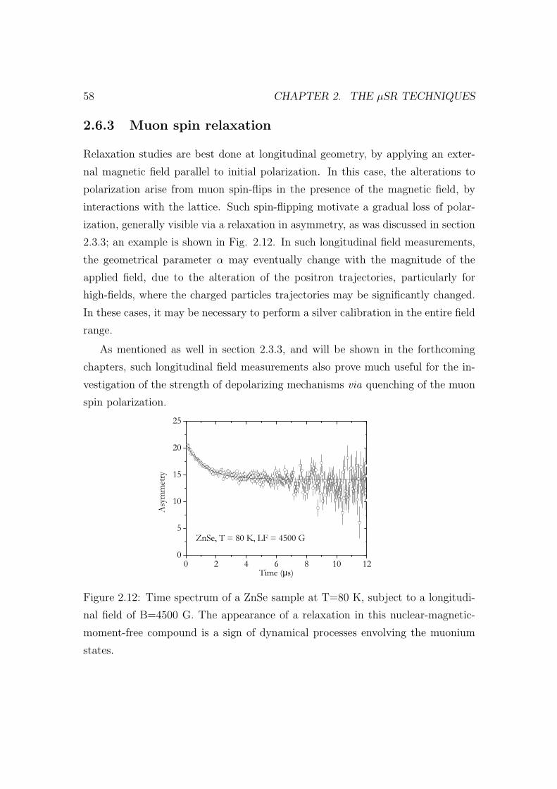
58 CHAPTER 2. THE µSR TECHNIQUES
2.6.3 Muon spin relaxation
Relaxation studies are best done at longitudinal geometry, by applying an exter-
nal magnetic field parallel to initial polarization. In this case, the alterations to
polarization arise from muon spin-flips in the presence of the magnetic field, by
interactions with the lattice. Such spin-flipping motivate a gradual loss of polar-
ization, generally visible via a relaxation in asymmetry, as was discussed in section
2.3.3; an example is shown in Fig. 2.12. In such longitudinal field measurements,
the geometrical parameter α may eventually change with the magnitude of the
applied field, due to the alteration of the positron trajectories, particularly for
high-fields, where the charged particles trajectories may be significantly changed.
In these cases, it may be necessary to perform a silver calibration in the entire field
range.
As mentioned as well in section 2.3.3, and will be shown in the forthcoming
chapters, such longitudinal field measurements also prove much useful for the in-
vestigation of the strength of depolarizing mechanisms via quenching of the muon
spin polarization.
0 2 4 6 8 10 120
5
10
15
20
25
ZnSe, T = 80 K, LF = 4500 G
Asym
metry
Time (µs)
Figure 2.12: Time spectrum of a ZnSe sample at T=80 K, subject to a longitudi-
nal field of B=4500 G. The appearance of a relaxation in this nuclear-magnetic-
moment-free compound is a sign of dynamical processes envolving the muonium
states.

2.6. MUON SPIN ROTATION, RELAXATION, RESONANCE 59
2.6.4 Muon spin resonance
As we have pointed out in section 2.3.1, the occurrence of muon spin depolarization
in the muon thermalization process and/or the existence of muon charge/spin dy-
namics may lead to a ”missing fraction” in the polarization, as seen in transverse- or
longitudinal-field measurements, thus hiding the nature of the final state. However,
if a given state is present, albeit depolarized, its presence may be demonstrated by a
change in the longitudinal field polarization induced by forcing transitions between
the corresponding spin levels, by means of resonant electromagnetic radiation.
In this muon-spin resonance method, one basically begins with a longitudinal-
field configuration, and then force the transitions between the spin energy-levels in
the presence of the static longitudinal field, by means of electromagnetic radiation.
For the most common case where the final-state, analyzed through this method,
is a diamagnetic state, the spin-level transitions are determined (as will be further
detailed below) by the muon gyromagnetic ratio γµ = 135.5 MHz/T and thus
fall on the radio-frequency domain. This subtechnique is thus also commonly
designated radio-frequency-µSR (RF-µSR). However, final-state analysis of para-
magnetic states is also possible, despite being harder and less common, in which
case the much higher energy differences between hyperfine levels for a given field
are best dealt with microwave radiation [Kre94]. The principle is nevertheless the
same and the acronym RF-µSR will be often used throughout this work even for
the microwave case.
As we shall see, this method allows the extraction of quantitative information
about the state under investigation. In this work, we shall concentrate on the
usual RF in diamagnetic or deep paramagnetic states. The details for the novel
shallow muonium states found in the cadmium chalcogenides may be somewhat
different, in spite the principles being the same. However, the extreme low values
of the hyperfine interaction in these materials scale down the corresponding Breit-
Rabi diagram several orders of magnitude, and reveal some subtleties unknown
to the usual studies, such as excitation of the ESR levels and the corresponding
RF-induced repolarization features [Cox03b, Lor04]. Usually, though, the forced
transitions in muon-spin-resonance methods further depolarize the muon spin.

60 CHAPTER 2. THE µSR TECHNIQUES
Basic principle
The basics of the RF technique are more easily explained in a (pseudo)-classical
precession model in a rotating reference frame [Kre90].
As known, a magnetic moment ~µ = γ ~J subject to a static magnetic field
~B = Bk precesses around the field due to the torque d ~J/dt = ~µ × ~B, with the
Larmor frequency ω0 = γ B. The magnetic moment precesses in a constant-energy
conical surface with constant angle with the applied field, so that its component
in the k direction remains constant. When applying a circularly polarized radio-
frequency field ~Brf perpendicularly to the static field
~Brf(t) = B1 [cos(ωt + φ) ı + sin(ωt + φ) ] (2.78)
the effective field becomes, in a reference frame ıR, R, k rotating with the rf-field
frequency ω around k,
~Beff =ω0 − ω
γk + B1 p (2.79)
where p = p(φ) = cos φ ıR + sin φ R.
From eq. 2.79, we regain the trivial Larmor precession in the trivial case where
no rf-field is applied, B1 = 0, so that the muon spin precesses with frequency
ω0 − ω in the frame rotating with frequency ω. This implies the spin is static
when ω = ω0, which corresponds to precession at the Larmor frequency ω0 in the
laboratory frame.
If the rf-field is at resonance with the magnetic moment precession (i.e., ω =
ω0 = γ B), then
Beff = B1p (2.80)
and the spin precesses, in the rotating reference frame, around the p direction with
frequency ω1 = γ B1.
In the general off-resonance case, the effective field in the rotating reference
makes an angle θ with the k direction, defined by:

2.6. MUON SPIN ROTATION, RELAXATION, RESONANCE 61
tan θ =ω1
ω0 − ω(2.81)
so that
Beff = cos θk + sin θp (2.82)
Considering the longitudinal field configuration, where the initial spin polar-
ization P = P k is parallel to k, we have, in the general off-resonance case as
seen through the rotating reference frame (please refer to fig. 2.13), a polarization
component P‖ = P cos θ parallel to the effective-field which is kept constant. The
polarization component P⊥ = P sin θ perpendicular to the effective-field precesses
around Beff , with the effective frequency ωeff :
ωeff =√
(ω0 − ω)2 + ω21 (2.83)
P|
P0
Beff
q
P||
k
Figure 2.13: Polarization considered on a rotating reference frame: the polariza-
tion component P⊥ precesses around the effective-field Beff , whereas the parallel
component P‖ is locked. The final polarization z component in the laboratory
reference frame is composed of the corresponding projections of P⊥ and P‖.
62 CHAPTER 2. THE µSR TECHNIQUES
So, the component Pk of the polarization in the k direction becomes:
Pk = P‖ cos θ + P⊥ cos(ωefft) sin θ
= P0
(cos2 θ + sin2 θ cos(ωeff t)
)(2.84)
Generally, radio-frequency measurements are done in time-integral mode:
Pk = νµ
∫ ∞
0
P0
(cos2 θ + sin2 θ cos(ωeff t)
)e−νµ t dt
= P0 cos2 θ + P0 sin2 θν2
µ
ν2µ + ω2
eff
(2.85)
So, the difference between the polarization when the radio-frequency is applied
(RF-on), Pon, and the polarization when the radio-frequency is off (RF-off), Poff ,
becomes:
Poff − Pon = P0 − P0 cos2 θ − P0 sin2 θν2
µ
ν2µ + ω2
eff
= P0 sin2 θω2
eff
ν2µ + ω2
eff
(2.86)
and, attending to eq. 2.81 (implying that sin2 θ = ω21/ω
2eff), we obtain
Poff − Pon = P0ω2
1
ν2µ + ω2
1 + (ω0 − ω)2(2.87)
This represents a lorentzian-shaped curve centered in the resonance frequency.
At resonance (ω = ω0), for ω1 >> νµ, the initial polarization P0 arises directly.
This implies B1 >> 33 G, which is however usually not the case.
An alternative way to the simple computation of the difference between the RF-
on and RF-off situations, is to define a RF-asymmetry as follows [Kre90, Kre95]:
Arf =N on
F −N offF
N onF −N off
F
− N onB −N off
B
N onB −N off
B
(2.88)
2.6. MUON SPIN ROTATION, RELAXATION, RESONANCE 63
The RF-asymmetry in eq. 2.88 is most commonly used and can be demon-
strated [Kre90, Kre95] to have the same lorentzian dependence shown for the po-
larization difference 2.87.
Experimental praxis
Detailed descriptions of the radio-frequency setup at the ISIS Facility and of the
microwave setup at TRIUMF, which were both used in this work, can be found
in references [Jon04] and [Kre94]. Here we shall limit to some essential points in
the conduction of a typical RF experiment. Pulsed muon sources provide here less
problems due to RF-heating, since the RF excitation may be turned on and off
synchronically with the beam pulses [Cot00].
A specific RF cavity is needed for these experiments, where the sample is placed
inside a non-ferromagnetic non-conducting target cell. There, the sample (itself
non-ferromagnetic and non-conducting) is surrounded by a coil (usually designed
as a solenoid) which produces the B1 field created by the RF current delivered by
an appropriately matched RF signal generator and amplifier. The sample holder
itself should be non-conducting non-ferromagnetic. For the experiments at ISIS,
mylar sample holders specifically cut for each sample were used. The sample was
glued at the sample holder with varnish, after being involved in (insulating) kapton
tape, and subsequently in adhesive copper tape, used as the solenoid coil. This
copper tape was further connected to the RF circuit.
In order to obtain calibration of the intrinsic asymmetry o the setup, a non-
conducting calibration material must be used. Polyethene is a usual choice, with a
polarization from a diamagnetic state of about 66%. The calibration measurements
for each sample are performed in two steps: (i) measurement of the diamagnetic TF
polarization of a polyethene sample cutted with the same shape of the sample under
research, by comparison with a silver sample; (ii) measurement of the maximum
RF asymmetry for the polyethene sample, by means of a resonance curve.
We present in figure 2.14 an example of a lorentzian resonance observed for
polyethene. The usual experimental procedure is to fix the excitation frequency
and vary the amplitude of the static field. This turns out to be simpler and more

64 CHAPTER 2. THE µSR TECHNIQUES
reliable than changing ω1. Thus, after fixing the excitation radio-frequency ω1 and
the corresponding excitation power at some adequate value in order to be able to
appropriately define a resonance curve within the values of the static field accessible
experimentally. The static field is thus varied around the resonance field (ω1/γµ, for
RF-µSR studies of diamagnetic states). In the course of the experiment, different
histograms are accumulated for the RF-on and the RF-off situations. An example
is shown in figure 2.15.
Usually, the information is extracted from the time-integrated RF asymmetry
ARF . However, as can be seen from fig. 2.15, the weak precession about the B1
field can nevertheless be observed in the RF-on time spectrum. Some authors
have therefore dedicated some effort to the interpretation of the time-differential
RF-µSR data, particularly regarding the determination of parameters of muonium
conversion [Cot03, Mor86, Nis85]. However, such studies are seldom used, due to its
extreme statistics-accumulation demands in order to clearly define the precessions
around the B1 field.
1850 1900 1950 2000 2050
-0.125
-0.100
-0.075
-0.050
-0.025
0.000
Avera
ge asy
mmetr
y diffe
rence
B (G)
Figure 2.14: A lorentzian resonance curve obtained for polyethene at T=290 K.
The excitation frequency is 26.2 MHz.

2.6. MUON SPIN ROTATION, RELAXATION, RESONANCE 65
0 2 4 6 8 10
-0.2
-0.1
0.0
0.1
0.2 polyethene
Asym
metry
Time (µs)
Figure 2.15: Radio-frequency µSR time spectrum for polyethene at T=290K. Black
circles denote ”RF-on” and white circles represent ”RF-off”. The static field is
B=1934 G, corresponding to the lorentzian’s peak in fig. 2.14, matching the reso-
nance condition 2πγµB = 26.2 MHz for the applied RF excitation frequency.

66 CHAPTER 2. THE µSR TECHNIQUES
2.6.5 User facilities and spectrometers
The muon production process requires a proton accelerator capable of reaching
hundreds of MeVs. Such accelerators exist only in large-scale installations. Cur-
rently, the following muon user facilities exist in four laboratories around the world:
• ISIS pulsed muon facility [ISI07] at the Rutherford Appleton Laboratory, in
the United Kingdom;
• Laboratory for muon spin spectroscopy [PSI07] at the Paul Scherrer Institut,
in Switzerland;
• Centre for molecular and materials science [TRI07] at the Tri-University Me-
son Facility (TRIUMF), in Canada;
• Meson science laboratory [KEK07] at KEK, in Japan. This muon facility
has been shut down on March 31, 2006 [Kad07], and a new facility (J-PARC
Muon Facility) is currently under construction, muon beam delivery to users
being planned to 2009 [Miy06].
In this work, we have used the spectrometers EMU [ISI04] at ISIS, HELIOS and
HITIME at TRIUMF, and GPS [Ama05] and DOLLY at PSI. Each has particular
characteristics and capabilities. We shall describe them briefly now and point the
specific use of each facility in this work.
ISIS
The ISIS facility at the Rutherford–Appleton Laboratory, in the United King-
dom, has a pulsed 800 MeV proton beam. The simple pulse has a full width at
half-maximum of 80 ns; such width limits the maximum observable frequency to
about 10 MHz. Muons are produced by proton collisions on a few-millimeters
graphite target, placed at 45o with the proton beam. Surface muons with momen-
tum 26.5 MeV/c and c. 3.2 MeV are extracted, corresponding to a stopping power
of about 100 mg/cm2. The muon beam intensity is about 4× 10⁵ muons/s, which
is divided among the three experimental areas EMU, MuSR and DEVA, allowing
typical accumulation rates of 10–20 millions of events per hour.

2.6. MUON SPIN ROTATION, RELAXATION, RESONANCE 67
EMU The EMU instrument is optimized for measurements in zero field and
longitudinal field. The positron detectors are basically 32 cintillating segments
placed in two circular rows of 16 detectors each. The rows are placed so that
the incoming beam coincides with the symmetry axis. The detectors signal is
transferred by light guides to nearby photomultipliers, so that local magnetic fields
do not affect the electronics.
It is possible to apply longitudinal fields up to 4000 G (0.4 T) with a set of
Helmholtz coils. A set of ancillary coils allows transverse-field measurements up to
100 G (0.01 T). A further set of ancillary coils does the automatic compensation
of the Earth’s magnetic field with a precision better than 30 mG.
A wide range of temperatures is accessible with the available cryostats and
furnaces. A simple closed-cycle cryostat allows measurements in the 2 K - 360 K
range. Two other cryostats allow reaching temperatures as low as 350 mK. A
furnace allows extending the temperature range from room temperature up to
1000 K.
A fly-past method has been developed at EMU in order to allow measurements
almost with no background, even in the smallest samples: this flypast method
simply consists of a long tube placed longitudinally after the sample, so that muons
which do not hit the sample fly to the tube and decay there, therefore minimizing
as much as possible its contribution to the background. This implies a sample
holder specifically designed to be as thin as possible and be entirely covered by
even the smallest samples, so that muon stopping in the holder is prevented.
In recent years, radio-frequency facilities have been developed at ISIS, taking
advantage of the pulsed nature of the beam, which prevents the heat-up problems
found at continuous sources [Cot00, Cot03]. An optical reflector furnace has most
recently been developed that allows measurements above room temperature, up to
1300 K. This was used for muon-spin resonance measurements in the course of this
work, and the experimental data acquired with this new capability count among
the very first results obtained with it.

68 CHAPTER 2. THE µSR TECHNIQUES
PSI
The Paul Scherrer Institut, in Switzerland, has a quasi-continuous beam of 590 MeV
protons. 28 MeV/c muons are gathered in a beam with polarization greater than
95%. Before arriving to the sample, the muon beam is directed through a spin-
rotator, which turns the muon spin–polarization with respect to the linear momen-
tum from an angle variable between 6 and 60o.
Unlike ISIS, the proton beam at PSI is continuous, so that the time resolution is
limited essentially by the resolution of the positron detectors, thus allowing access
to much higher frequencies (typically hundreds of MHz).
General Purpose Instrument (GPS) and its clone DOLLY The GPS spec-
trometer, and its clone DOLLY, are optimized for transverse-field experiments.
They have 5 positron detectors, placed in the forward (F), backward (B), up (U),
down (D), and right (R) positions (all the positions are referred to the incoming
beam direction). The setup also includes a muon detector before the sample (which
starts the clock) and two veto detectors (veto-B and veto-F). The veto-B detector
is a pyramidal cintilator with a small 7× 7 mm hole in front of the muon detector.
This detector serves for collimating the muon beam, and rejects the muons (and
the corresponding positrons) missing the hole. The veto-F detector rejects the
muon (and respective positron) signal for muons that do not stop in the sample,
and is particularly useful for investigations on small samples. For samples large
enough, this detector can be coupled to the F detector, and used to enlarge the
solid angle for detection.
In order to deal with the high beam-borne background typical of a high repeti-
tion rate quasi-continuous source, a ”Muons-On-REquest” setup is available, which
reduces the background by at least a factor of 100 [Ama05].
The experimental setup includes a continuous He-flow cryostat, for the 2 to
300 K range, and a set of coils for magnetic fields up to 6000 G (0.6 T) in the
direction of the incoming beam. Compensation of the Earth’s magnetic field is
usually better than 0.1 G in every direction. A furnace is also available, allowing
to extend the temperature range up to 800 K.

2.6. MUON SPIN ROTATION, RELAXATION, RESONANCE 69
TRIUMF
Similarly to PSI, TRIUMF has a quasi-continuous muon beam. Two dedicated
beamlines, M15 and M20, are used for positive-muon spin investigations. We have
used the HITIME spectrometer in the M15 line and the HELIOS spectrometer in
the M20 line.
HITIME at the M15 beamline. The M15 beamline is dedicated to surface
µ+ from a 1cm graphite or beryllium proton target. The muon’s momentum range
goes from about 19 MeV/c to 40 MeV/c. Dual spin-rotators in the M15 line both
separate positrons from the beam and rotate the muon spin to be perpendicular
to the beam direction.
The High-Time spectrometer is based on a superconducting magnet dedicated
to studies with high transverse fields and high frequencies. The magnet is a su-
perconducting split solenoid delivering 7.5 T at its maximum current of 100 A.
The cryostat is a hybrid between a gas flow and cold finger cryostat as the helium
flow is through a ring around the sample area - the sample is cooled by helium
exchange gas surrounding it. The counters are small size cintilators, adequate for
high-time resolution at high transverse fields. Spin rotated muons are used. The
HITIME spectrometer has been designed so that a 8 × 8 mm sample is enclosed
inside the cintilators. This ingenious design, together with the extremely high
field attainable, transform this spectrometer into an extremely powerful tool for
high-resolution spectroscopic measurements.
HELIOS, in the M20 beamline Although it can be used as a (high momen-
tum) decay muon beamline, M20 is, effectively, a dedicated (low momentum: 29
MeV/c) surface-muon channel. It takes muons from a 10-cm Be target. Its spin
rotator can provide clean beam with longitudinal or transverse (spin-rotated) po-
larization.
Helios is a superconducting magnet, which provides 6.7 T at its maximum
current of 70 A. The main counter array is for solid state work in narrow cryostats,
and there is another set of counters for larger samples such as gas cells. Both sets

70 CHAPTER 2. THE µSR TECHNIQUES
have long light guides and poor timing resolution (≥ 1 ns). All access is axial, but
the large bore makes this a versatile magnet, allowing experiments in longitudinal
field and transverse field. A microwave setup has been developed for using with
this spectrometer. This setup pioneered muon spin resonance measurements in
paramagnetic states [Kre94] and keeps its status as the best instrument for such
investigations.
Final remarks
In short, the specific advantages of each facility may be summarized as follows: high
resolution, low background, spectroscopic measurements are possible at TRIUMF
with its high magnetic field capabilities. The extension to high-temperatures is
however only possible at PSI, which, despite lower fields, has a versatile furnace
setup. ISIS, as a pulsed source, can not compete with such high resolutions, but the
existence of pulsed radio-frequency capabilities from liquid-helium temperatures up
to much above room temperature (c. 1300 K), allows deeper research by RF-µSR
final-state analysis of diamagnetic states.

Chapter 3
Sample characterization
Contar-te longamente as perigosas
Cousas do mar, que os homens nao entendem,
Subitas trovoadas temerosas,
Relampagos que o ar em fogo acendem,
Negros chuveiros, noites tenebrosas,
Bramidos de trovoes que o mundo fendem.
Nao menos e trabalho que grande erro,
Ainda que tivesse a voz de ferro.1
Luıs Vaz de Camoes
Os Lusıadas, V, 16
3.1 Introduction
The samples used in this work were obtained either commercially or from other
investigation groups which had previously done research on these materials. Not
much information was available about the samples, particularly for the ones ob-
tained commercially, except for very general descriptions such as ”nominally un-
doped”.
1Free translation: ”Tell you extensively the dangerous things of the sea, that men do not
understand, sudden frightening storms, lightnings firing the air, dark rains, tenebrous nights, the
roar of thunders breaking the world. It is no less effort than big mistake, even if I had an iron
voice.”

72 CHAPTER 3. SAMPLE CHARACTERIZATION
In the course of this investigation, an urgency for sample characterization grew
immensely with the accumulation of µSR experimental data on different samples of
the same material (especially ZnSe), which showed different features related to the
interaction of the muon with electrons in the material, as will be described in detail
in Chapter 4. The need was particularly felt to have basic transport measurements
(resistivity and Hall-effect) which might give some information regarding the con-
centration of conduction electrons. Conscious of the many experimental difficulties
associated with this kind of measurements, particularly those related to establish-
ing ohmic contacts in highly-resistive samples, the first efforts were directed to
find other research groups specialized in these measurements, in order to establish
some colaboration. However, establishing ohmic contacts in bulk ZnSe seems to
be a rare and disappearing art.
Already at the final stages of this work, and attending to the simplicity of
the basic experimental physics involved in doing Hall-effect and resistivity mea-
surements, the decision was taken of trying to establish a modest Hall-effect and
resistivity setup in Coimbra and thus try to obtain at least order-of-magnitude val-
ues for the resistivity of our ZnSe samples. Despite the difficulties and the limited
results obtained up to now, this setup allowed to estimate the resistivity of our
samples, and may thus be considered as a declaration of capability, to improve in
the future. The obtained results, although minimal, already shine much light on
the observed sample differences.
3.2 Samples
3.2.1 ZnSe
In the beginning of this work, the samples were simply acquired commercially
from usual suppliers, such as Crystec and Alpha-Aesar. The initial µSR measure-
ments were performed in two nominally undoped single crystals from these two
companies, labeled ”AA” and ”Ctec”. In order to have the possibility of inves-
tigating anisotropy effects, oriented single crystals from the same batch, cutted
along different crystallographic orientations, were bought as well. The crystallo-

3.2. SAMPLES 73
graphic orientations were checked by X-ray diffraction with the help of the physical
crystallography group at Coimbra. All these samples are nominally undoped.
Later on, we established a contact with the team of K. Irmscher and D. Siche at
the Institut fur Krystal-Forschung Berlin (IKF-Berlin), who had done some work
on the growth of ZnSe in the 90’s. Though the research topic of this team has
meanwhile moved towards other interests, they have kindly gave us three ZnSe
samples: two samples grown by chemical vapour transport (CVT) and one grown
by the Bridgmann method. The chemical agent used in the CVT growth is I2
[Bot01], which implies always a doping, even if unwanted, with the iodine donor
[Chi83]. Thus the two CVT samples (labelled ”CVTu” and ”CVT:I ”) are doped:
CVTu undeliberately and CVT:I deliberately.
We should emphasize that, in spite of the absence of intentional doping in all
the samples except CVT:I, we expect all the samples to be n-type, as known for
ZnSe and discussed in chapter 1. Of course, different concentrations of free car-
riers are expected, according to the different concentration of electrically active
impurities and defects, whose presence is evidenced by photoluminescence mea-
surements to be presented, and according to the degree of compensation. Among
the compensating centres, the zinc vacancy VZn plays a special role in ZnSe, as
mentioned in chapter 1: it has been shown to form complexes with donors, and
this process can be reversibly controlled by thermal annealing in zinc atmosphere
[Geb02, Irm01, Pro00], thus allowing to control the concentration of conduction
electrons and therefore the conductivity. This has prompted us to try to change
the concentration of conduction electrons of one of the samples, in order to change
the formation probability of the muonium states observed. In this context, we
have annealed a piece of the [100] Ctec sample in zinc atmosphere, for 100 hours at
900oC. For the annealing, the sample was sealed in primary vacuum, together with
2 mg of zinc (99.9998% purity) in a 6-mm diameter quartz tube with about 8 cm
length. The resulting sample was labelled Ctec:Zn and the degree of compensation
by zinc vacancies is expected to be less than in the original Ctec sample, thus
presenting a smaller resistivity and a higher ”net” concentration of free carriers.
A resume of the used ZnSe samples can be found in table 3.1.

74 CHAPTER 3. SAMPLE CHARACTERIZATION
Name Company/Laboratory Doping Other information
AA Alpha-Aesar undoped -
Ctec Crystec undoped [100], [110] and [111] orientations
Ctec:Zn Crystec undoped Ctec [100] annealed in Zn atmosphere
CVTu IKF-Berlin ”undoped” CVT grown
CVT:I IKF-Berlin Iodine doped CVT grown
B IKF-Berlin undoped Bridgmann-grown
Table 3.1: Monocrystalline ZnSe samples used in this investigation. Though all the
samples, except CVT:I are nominally undoped, ZnSe presents n-type conductivity,
as mentioned in chapter 1. In the case of the CVTu sample, the CVT growth
implies unintentional doping with the shallow donor iodine.
Basic photoluminescence characterization
A very basic characterization by photoluminescence was done with the photolu-
minescence apparatus at the Physics Department of the University of Aveiro. All
the samples in table 3.1 were checked, except the Ctec:Zn piece resulting from an-
nealing the Ctec sample in zinc atmosphere. The measurements were done inside
a closed-cycle cryostat at 15 K. The 325 nm ultraviolet line of He-Cd laser was
used for the optical excitation. The study of the dependence of the intensity of
the luminescence light was done as usually [Mon05] by means of a photomultiplier
attached to a monochromator.
The results for the near band edge photoluminescence are shown, for samples
AA, Ctec, CVTu, CVT:I and B, in Figs. 3.1, 3.2, 3.3, 3.4 and 3.5, respectively.
The essential features of the spectra can be readily interpreted, with the help
of the vast amount of photoluminescence literature on ZnSe.
The Fx peak is associated with the free exciton and is an intrinsic property of
the samples, usually associated with crystalline perfection [Su01, Tri96]. We find it
at 2.8038 eV for the AA and Ctec samples and at 2.8013 eV for the CVTu sample.

3.2. SAMPLES 75
2.60 2.65 2.70 2.75 2.800.0
0.1
0.2
0.3
0.4
F
I
I
AA
PL in
tensity
(10 a.u
.)
Energy (eV)
Figure 3.1: Near-band-edge photoluminescence spectrum of the undoped ZnSe
single crystal from Alfa Aesar (AA sample), at 15 K. The free-exciton Fx line, the
donor-bound exciton I2 line, and the deep-acceptor-bound exciton I1 line (with its
phonon replicas), may be readily identified with the existing literature support.
2.60 2.65 2.70 2.75 2.800.0
0.1
0.2
0.3
IFI
Ctec
PL in
tensity
(10 a.u
.)
Energy (eV)Figure 3.2: Near-band-edge photoluminescence spectrum of the undoped ZnSe
single crystal from Crystec (Ctec sample), at 15 K. The same basic features present
in the AA sample (see Fig. 3.1) are visible.

76 CHAPTER 3. SAMPLE CHARACTERIZATION
2.60 2.65 2.70 2.75 2.800.0
0.2
0.4
0.6
0.8
1.0
1.2
DAP
FCVTu
PL in
tensity
(10 a.u
.)
Energy (eV)
Figure 3.3: Near-band-edge photoluminescence spectrum of the ”undoped” (i.e.,
undeliberately doped with iodine) ZnSe single crystal grown by CVT and obtained
from the IKF-Berlin group (CVTu sample). The spectrum was obtained at a
temperature of 15 K. Aditionally to that observed in the AA (Fig. 3.1) and in the
Ctec (Fig. 3.2) samples, a strong donor-acceptor pair (DAP) line and its phonon
replica is observed. Of note, the strong intensity of the free-exciton Fx line, a sign
of crystalline perfection. It probably overwhelms the weaker I2 line.

3.2. SAMPLES 77
2.60 2.65 2.70 2.75 2.800.00
0.01
0.02
0.03
0.04
I
I
CVT:I
PL in
tensity
(10 a.u
.)
Energy (eV)Figure 3.4: Near-band-edge photoluminescence spectrum of the (deliberately)
iodine-doped ZnSe single crystal grown by CVT and obtained from the IKF-Berlin
group (CVT:I sample). The spectrum was obtained at a temperature of 15 K.
The luminescence of this sample is very weak, but I1 and I2 emission seem to be
present. A peak of unknown origin is observed at 2.764 eV.
2.60 2.65 2.70 2.75 2.800.0
0.1
0.2
0.3
0.4
DAP
I
F
I
B
PL in
tensity
(10 a.u
.)
Energy (eV)
Figure 3.5: Near-band-edge photoluminescence spectrum of the undoped ZnSe
single crystal grown by the Bridgmann method and obtained from the IKF-Berlin
group (B sample). The spectrum was obtained at a temperature of 15 K. Fx, I2,
I1 (with replica) and DAP (with replica) lines, as in the previous samples, are
observed.

78 CHAPTER 3. SAMPLE CHARACTERIZATION
Such small variations between samples are also found in the cited literature. This
emission is also visible in the B sample as a ”shoulder” in the I2 emission.
The Ideep1 emission is followed by longitudinal-optical-phonon (LO) replica at
intervals of 31 meV. We observe it at 2.786 eV for the B sample, at 2.785 eV for
the CVTu sample, at 2.784 eV for the AA and Ctec and, possibly, at 2.783 eV
for the CVT:I sample. Two origins seem to coexist for this emission: an exciton
bound to a deep Zn vacancy (VZn) acceptor or to a copper impurity substituting
at a zinc site CuZn [Iss88].
I2 emission is found at 2.798 eV in the Ctec sample and at 2.799 eV in the
AA, B and CVT:I samples. It ”has been attributed to the exciton bound to a
substitutional neutral donor, such as Al, Ga, In on the Zn site or Cl and F on the
Se site” [Su01].
In the CVTu and B samples, donor-acceptor pair(DAP) emission is also present
(at 2.699 eV in the CVTu and at 2.698 eV in the B), together with the respective
LO replica with 31 meV intervals. Su et al. identify it with the DAP associated
with the Li or Na acceptor [Su01].
In these brief photoluminescence measurements, we have observed intense deep-
level emission as well, visible in the lower energy region of the photoluminescence
spectra. These are depicted in Figs. 3.6, 3.7, 3.8, 3.9 and 3.10, for samples AA,
Ctec, CVTu, CVT:I and B, respectively. Please note that the band-edge emission
part (2.57 - 2.82 eV) of these figures has already been represented in figs. 3.1, 3.2,
3.3, 3.4 and 3.5.
Three main bands appear, usually known in the literature as the ”red band”
(c. 1.94 eV), the ”yellow” band (c. 2.17 eV) and the ”green” band (c. 2.34 eV)
[Mal88, Par72, Pla00, Pla03, Str68].
The ”red” band arises from a superposition of luminescence with two different
origins [Pla03]. One contribution is from self–activated luminescence arising from
a complex involving a zinc vacancy and a group-III or group-VII donor: such
complex behaves as an acceptor and the luminescence arises from recombination
of donor electrons with the acceptor holes [Bou75, Pla03]. The other contribution is
from the well-known transitions either from the conduction band or from shallow–

3.2. SAMPLES 79
1.6 1.8 2.0 2.2 2.4 2.6 2.80.00.10.20.30.40.50.60.70.8
AA
PL in
tensity
(10 a.u
.)
Energy (eV)
Figure 3.6: Deep-level photoluminescence emission for the ZnSe AA sample, at
15 K. ”Red” (c. 2.0 eV) and ”green” (c. 2.3 eV) bands are observed and, possibly,
also an ”yellow” (c. 2.1 eV) band.
1.6 1.8 2.0 2.2 2.4 2.6 2.80.00.61.21.82.43.03.64.2
Ctec
PL in
tensity
(10 a.u
.)
Energy (eV)Figure 3.7: Deep-level photoluminescence emission for the ZnSe Ctec sample, at
15 K. A strong ”red” (c. 2.0 eV) and a weaker ”green” (c. 2.3 eV) bands are
clearly distinguishable.
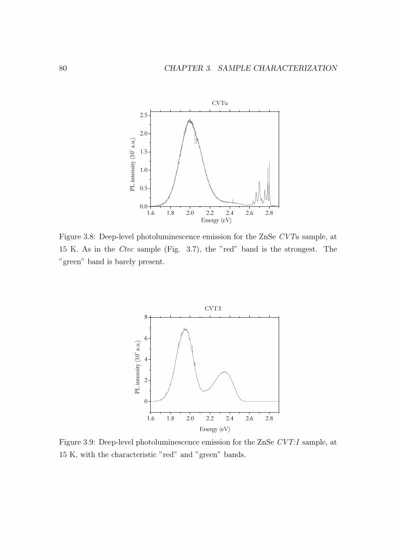
80 CHAPTER 3. SAMPLE CHARACTERIZATION
1.6 1.8 2.0 2.2 2.4 2.6 2.80.0
0.5
1.0
1.5
2.0
2.5 CVTu
PL in
tensity
(10 a.u
.)
Energy (eV)
Figure 3.8: Deep-level photoluminescence emission for the ZnSe CVTu sample, at
15 K. As in the Ctec sample (Fig. 3.7), the ”red” band is the strongest. The
”green” band is barely present.
1.6 1.8 2.0 2.2 2.4 2.6 2.8
0
2
4
6
8
CVT:I
PL in
tensity
(10 a.u
.)
Energy (eV)Figure 3.9: Deep-level photoluminescence emission for the ZnSe CVT:I sample, at
15 K, with the characteristic ”red” and ”green” bands.

3.2. SAMPLES 81
1.6 1.8 2.0 2.2 2.4 2.6 2.80.000.020.040.060.080.100.120.140.16
B
PL in
tensity
(10 a.u
.)
Energy (eV)
Figure 3.10: Deep-level photoluminescence emission for the ZnSe B sample, at
15 K. Of note, the similar intensities of the ”red”, ”yellow” and ”green” bands.
donor levels to the empty CuZn center [Str68]. We observe this ”red” band in
all samples, with peak energies ranging from 1.946 eV to 2.01 eV. Again, we find
similar differences in the literature. The adopted analysis may also shift slightly
the position of the peaks, depending on the number of contributions considered.
The ”green” band is associated with an acceptor defect that contains a zinc
vacancy [Heu92, Pla03]. Again, it is present in all samples, with peak energies
ranging from 2.281 eV to 2.396 eV.
Finally, the ”yellow” band is ocasionally observed [Bou75, Mal88, Par72] and
has been attributed to a defect involving aluminum and an alkaline impurity
[Bou75]. We observe it for the B sample at 2.139 eV and, eventually, also for
the AA sample at 2.1 eV.
These brief photoluminescence measurements already provide some insight into
the samples properties. Particularly, they clearly display the extremely rich inter-
play between defects and impurities in this material, where the same basic features
seem to be present in all samples (eventually with the exception of the doped
CVT:I sample), with small diferences arising from the incorporation of impurities
at the growth process.

82 CHAPTER 3. SAMPLE CHARACTERIZATION
3.2.2 ZnS and ZnTe
We have also investigated monocrystalline samples of the two other zinc chalco-
genides, ZnS and ZnTe. As mentioned in Chapter 1, these play nowadays a lesser
role in the technological applications, but its study imposes itself by fundamental
reasons and also in a systematic approach.
Two factors conjugate in the slighter weight of ZnS and ZnTe in this investi-
gation. The first arises from the µSR data itself: as will be shown in Chapters 4
and 5, we find in ZnSe a wealth of phenomena requiring deeper research. Secondly,
the research focus on ZnSe over the recent past has provided a vast amount of
information on this compound which allows more significant insight.
The ZnS and ZnTe samples investigated were all from commercial origin and
are compiled in table 3.2. Again, we should stress that, despite the samples are
nominally undoped, the already mentioned tendency of the II–VI semiconductors
to one type of conductivity is also present in ZnS, tipically n–type, and in ZnTe,
tipically p–type.
Name Company/Laboratory Doping Other information
ZnS Crystec undoped [110] and [111] orientations
ZnTe Crystec undoped [100],[110] and [111] orientations
Table 3.2: ZnS and ZnTe samples used in this investigation. Albeit they are
nominally undoped, ZnS is known to be n-type and ZnTe is known to be p-type.

3.3. RESISTIVITY AND HALL EFFECT IN ZNSE 83
3.3 Resistivity and Hall effect in ZnSe
As mentioned in this chapter’s introduction, the most delicate issue regarding the
aimed resistivity/Hall-effect measurements, is the establishing of ohmic contacts
in the material. We first discuss this point, before presenting the measurement
apparatus proper and discussing the obtained results.
3.3.1 Ohmic contacts
The electronics at a metal-semiconductor interface can be described in a simple way
by the simple Schottky model [Mil72, Nea97, Sze81]. For the case of a metal with
a work function φm larger than the work function φS of a n–type semiconductor,
φm > φS (Cf. Fig. 3.11 (a)), the thermal equilibrium condition (same chemical
potential EF over the metal-semiconductor system) implies a flow of electrons
from the semiconductor to the metal, leaving a depletion region of positively–
charged donors at the interface. As illustrated in Fig. 3.11 (b), this gives rise to a
barrier φm−χS for electrons flowing from the metal to the semiconductor and to a
barrier φm−φS for electrons flowing from the semiconductor to the metal, χS being
the electron affinity of the semiconductor. Whereas the metal–to–semiconductor
barrier φm−χS is insensitive, in idealized conditions, to a potential difference across
the metal–semiconductor interface, this is not the case for the semiconductor–to–
metal barrier φm − φS, which is reduced if a positive potential is applied to the
metal with respect to the semiconductor (forward bias), and is increased in the
opposite situation (reverse bias) [Nea97]2. Such metal-semiconductor contact is
therefore a rectifying contact, and this junction acts as a metal–semiconductor
diode, which happens to be one of the oldest known semiconductor applications,
dating from 1904 [Sze81]3.
If the metal work function φm is smaller than the semiconductor work function
φS, as depicted in Fig. 3.11 (c), we will now have a flow of electrons from the metal
to the semiconductor, creating a negatively–charged layer at the semiconductor
2Cf. pp. 308–312 of the cited reference.3Cf. p. 245 of the cited reference.

84 CHAPTER 3. SAMPLE CHARACTERIZATION
Figure 3.11: Energy level diagrams for a metal–semiconductor (type n) interface,
as in ref. [Mil72]. In the top, the situation for the case where the metal’s work
function φm is larger than the semiconductor’s work function φS (and the semi-
conductor electron affinity χS) (a). After establishing the contact (b), conduction
electrons face barriers φm − χS from the metal to the semiconductor and φm − φS
from the semiconductor to the metal, and the junction is rectifying. Below, the
corresponding situation for the case where φm < φS (c): no significant barriers
exist (d) and the contact is ohmic.

3.3. RESISTIVITY AND HALL EFFECT IN ZNSE 85
Figure 3.12: Energy level diagrams for a metal–semiconductor (type p) interface, as
in ref. [Mil72]. In the top, the situation for the case where the metal’s work function
φm is smaller than the semiconductor’s work function φS (and the semiconductor
electron affinity χS) (a). After establishing the contact (b), holes face barriers
χS−φm from the metal to the semiconductor and φS−φm from the semiconductor
to the metal, and the junction is rectifying. Below, the corresponding situation for
the case where φm > φS (c): no significant barriers exist (d) and the contact is
ohmic.

86 CHAPTER 3. SAMPLE CHARACTERIZATION
interface, affecting the band levels as in Fig. 3.11 (d). In this situation, electrons
can flow easily in each direction when a voltage (either positive or negative) is
applied to the metal with respect to the semiconductor. This junction is therefore
an ohmic contact.
The discussion above can easily be reproduced, mutatis mutandis, for a junction
between a metal and a p–type semiconductor. The corresponding energy diagrams
are shown in Fig. 3.12.
In order to access the electrical transport characteristics of a semiconductor,
electrical metal contacts with ohmic behaviour are required. At such contacts, and
for a not too small voltage range, the threshold voltage for zero current is negligible
with respect to the applied voltage and the proportionality between current and
voltage does not vary measurably with voltage [Kro56].
However, as pointed out by Sze, ”it is difficult to make ohmic contacts in wide-
gap semiconductors. A metal does not generally exist with a low-enough work
function to yield a low barrier. In such cases the general technique for making an
ohmic contact involves the establishment of a heavily doped surface layer such as
metal-n+-n or metal-p+-p contact by various methods, such as shallow diffusion,
alloy regrowth, in-diffusion of a dopant contained in the contact material, double
epitaxy, and ion implantation” [Sze81]4.
The investigation and development of ohmic contacts is therefore a task specific
to each semiconductor and which, despite the overall principles being basically un-
derstood for long [Kro56, Smi55], still occupies a considerable amount of research
effort, particularly in the wide–gap materials such as ZnSe, CdS and CdTe [Dar98],
and focusing recently in ZnO [Che06, Hu06, Kan06]. Of course, such investigations
are far off the main trend of this work, where we aimed at achieving but reason-
able ohmic contacts to ZnSe, in order to have some basic characterization of the
transport properties of our samples.
4Cf. p. 306 of the cited reference.

3.3. RESISTIVITY AND HALL EFFECT IN ZNSE 87
3.3.2 Ohmic contacts to ZnSe
The basic mechanism of formation of ohmic contacts to ZnSe has been investigated
by Kaufman and Dowbor [Kau74] and, despite recent improvements [Par99], it can
be taken as a guide for our objective. These authors build upon an already quite
established practice of obtaining ohmic contacts in ZnSe and other II-VI semi-
conductors by means of contacting with In metal [Ave63, Ave65, Dub70, Swa69],
either pure or alloyed with other elements. They suggest that, upon heating, In
dissolves ZnSe, forming a liquid-phase epitaxial layer which provides the ohmic
contact after cooling.
For the formation of such layer, Kaufmann and Dowbor emphasize the absolute
necessity of the In wetting the crystal, as evidenced by experiment. Therefore, the
optimum conditions for the formation of the contact include a clean surface and
the fusion of the In at the surface at a low temperature (around 300oC). The
presence of an inert atmosphere prevents the oxidation of the surface, hydrogen
being a usual choice (as it may act as an oxygen getter): Aven and Segall [Ave63]
electrode ZnSe with ”In dots fused-in under H2 atmosphere at 300oC”, Dubenskii
et al. refer that the ”In alloying was carried out in an atmosphere of purified H2
with rapid heating and cooling” [Dub70], Swank et al. inform that their samples
”were provided with ohmic contacts of indium, fired in hydrogen at 300oC for 30
s” [Swa69], Ray and Kroger acknowledge having heated the crystals ”for 2-3 min
to 300oC and then cooled to room temperature” [Ray78]. Introduction of hydrogen
into the sample (thereby affecting the electrical properties) is not expected to occur
for low temperatures and reduced annealing times [Hei59, Mol54].
Etching
Prior to applying the indium, the surface of the ZnSe crystals must be appropriately
cleaned. Again, many recipes are available in the literature, also due to the impor-
tance of having appropriate surfaces for optical studies. Though the earlier studies
only mention ”simple” procedures such as chemical polishing in hot concentrated
NaOH [Ave63], more recently many workers find adequate a multi-stepped etching,
in order to remove different kinds of surface imperfections [Nak97, Wen99]. We

88 CHAPTER 3. SAMPLE CHARACTERIZATION
adopted the following procedure: after degreasing the samples with standard sol-
vents (ethanol, acetone), we submitted them firstly to a chemical etching step in a
K2Cr2O7/H2SO4/H2O solution [Pro02, Sch94, Wen99]. Afterwards, the reduction
of the oxide layer was taken by etching in a HCl-H2O 1:1 solution and subsequently
in a 1:3 NH4OH(29%)-methanol solution [Chi83, Nak97]. The former is thought
to dissolve SeOx, and the latter ZnOx [Kim93]. The mentioned etching times vary
between 3 minutes [Pro02, Sch94] and 10 minutes [Chi83]. We adopted the latter
value for all steps.
After the etching, indium metal contacts (purity 99.998%) were placed, when-
ever possible, in the corners of the sample, as illustrated in Fig. 3.13. The samples
were then immediately placed in a quartz tube, in a H2 atmosphere.
Figure 3.13: Indium contacts on a ZnSe sample, placed at the four corners in order
to allow Hall-effect/resistivity measurements using the van der Pauw method. The
sample is shown before the thermal treatment applied in order to provide the ohmic
contacts.

3.3. RESISTIVITY AND HALL EFFECT IN ZNSE 89
Heat treatments
We have thus tried to obtain ohmic contacts by annealing the samples, prepared as
described previously, for some minutes at 300oC. A high-impedance electrometer,
for resistance measurements up to 210 TΩ (as well as corresponding DC current
and voltage measurements), was used to inspect the contacts electric behaviour:
the electrometer was used in current mode in order to measure the current through
the sample and contacts by applying a fixed dc voltage.
Rather unexpectedly, we found no linear behaviour, even for a sample annealed
for 30 minutes at 300oC (Fig. 3.14), but rather a non-ohmic I–V curve similar
to that obtained for a sample where the In contacts were simply soldered to the
sample.
However, we did find ohmic behaviour when annealing at 400oC for 30 minutes,
as shown in Fig. 3.15.
At 400oC, there should be no alteration of the conductivity of ZnSe due to dif-
fusion effects. The diffusion of In for the effect of doping is reported to occur only
at 900oC [Chi83]. Takenoshita et al. have measured the diffusion depth for this im-
purity and indicate only 10 µm, after a diffusion time of 10 hours at 600oC [Tak86].
Regarding self-diffusion in ZnSe, the respective coefficients have been measured by
Henneberg and Stevenson [Hen71] to be DZn = 9.8 exp(−3.0 eV/kT ) cm2s−1 and
DSe = 0.13 exp(−2.6 eV/kT ) cm2s−1. For estimating the corresponding diffusion
depth , we may use the simple relation between the diffusion coeficient D, the
diffusion depth X and the diffusion time t [Cra86, Jon94]
D =1
4t
(X
0.81
)2
(3.1)
From equation 3.1, the self-diffusion depth in ZnSe at 400oC, after annealing for
30 minutes, also corresponds to only some micrometers.

90 CHAPTER 3. SAMPLE CHARACTERIZATION
-80 -40 0 40 80-0.12-0.08-0.040.000.040.080.12
I (nA
)
V (V)
Figure 3.14: I–V curve obtained for a pair of contacts at a ZnSe sample annealed
for 30 minutes at 300oC. An unexpected non-linear behaviour shows up.
-80 -40 0 40 80-40
-20
0
20
40
I (nA
)
V (V)
Figure 3.15: I–V curve obtained for a pair of contacts at a ZnSe sample annealed
for 30 minutes at 400oC. A piece of the same sample as that shown in Fig. 3.14
was used.

3.3. RESISTIVITY AND HALL EFFECT IN ZNSE 91
Conclusion: adopted procedure
We have thus adopted the following procedure for obtaining ohmic contacts to
ZnSe:
• degrease the sample in acetone;
• chemical etching in K2Cr2O7/H2SO4/H2O solution for 10 minutes;
• etching in HCl-H2O 1:1 solution for 10 minutes;
• etching in 1:3 NH4OH(29%)-methanol solution for 10 minutes;
• immediately applying In contacts at the surface (as in Fig. 3.13) and placing
sample in a quartz tube at H2 atmosphere;
• heating in H2 atmosphere for 30 minutes at 400oC.
3.3.3 Resistivity and Hall effect measurements
We shall here briefly describe the basic principles and method used for the resistiv-
ity and Hall-effect measurements. These are standard techniques, and an essential
part of any semiconductor textbook, at all levels [Ash76, See82, Yu99]. Here, we
closely followed the procedure recommended by the US National Institute of Stan-
dards and Technology (NIST) [Ast00, Nis06], which is based upon the van der
Pauw four-point method [vdP58a, vdP58b].
Basic Hall effect
The basic Hall effect was first observed by E. H. Hall in 1879, while in a research
program to find magnetoresistive effects [Ash76]5. The Hall effect has since then
played a major role in the development of solid state physics, becoming a standard
technique for obtaining basic transport parameters, and being simultaneously at
the forefront of research, as is eloquently expressed by the unveiling of phenomena
as the quantum Hall effect (K. v. Klitzing, Nobel prize 1985) and the fractional
5Cf. pp. 11 and 12 of the cited reference.

92 CHAPTER 3. SAMPLE CHARACTERIZATION
quantum Hall effect (D. C. Tsui, H. L. Stormer and R. B. Laughlin, Nobel prize
1998) [Kli86, Lau99, Sto99b, Tsu99].
The basic Hall-effect measurement is depicted in Fig. 3.16. A magnetic field
B=B z k is applied perpendicularly to the face of a flat sample, subject to an
electric current due to an applied electric field E=E x ı. The charge-carriers in the
sample will be deflected in the y direction due to the Lorentz force
FL = q v ×B (3.2)
Figure 3.16: Schema of the basic Hall effect: a current j=j x ı flows due to the
application of an electric field E=E x ı, while the material is subject to an external
magnetic field B=B z k. The negative-charge carriers situation is depicted, where
the Lorentz force and the Hall electric field, in the reference frame of the figure,
point in the negative y direction. The width w and depth d of the sample are also
indicated.

3.3. RESISTIVITY AND HALL EFFECT IN ZNSE 93
The charge therefore accumulates in one of the y faces of the sample, thus
creating a y-component of the electric field against the Lorentz force. A potential
between the two y faces arises, named Hall potential. In the steady state, these
two forces in the y direction mutually cancel. The velocity of the charge carriers,
in this situation, is v=vx ı. The current density, in the steady state, is also only
in the x direction, according to
j = n q v (3.3)
The sign of the final Hall potential depends on the sign of the charge carriers.
As a matter of fact, for positive charge carriers such as holes, we have (see the
referential in Fig. 3.16) vx > 0, (q v ×B)y < 0 and therefore Ey > 0; for negative
charge carriers such as as electrons, it is vx < 0, (q v × B)y < 0 and therefore
Ey < 0; this last case is illustrated in Fig. 3.16.
In the classical relaxation time approximation (Drude model) [Ash76], the dy-
namics of negative charge carriers is described by (similarly to positive charge
carriers):
dp
dt= −eE− e
mp×B− p
τ(3.4)
where p/τ is a friction term and τ is the mean collision time. In the steady-state,
dp/dt = 0 and vy = 0. Eq. 3.4 becomes
−eEx =px
τ(3.5)
eEy =e
mpx B (3.6)
and, attending to eq. 3.3, we finally get:
jx =n e2 τ
mEx (3.7)
Ey = − 1
n eB jx (3.8)
The same result for jx and Ey is obtained if positive charge carriers are consid-
ered.

94 CHAPTER 3. SAMPLE CHARACTERIZATION
The conductivity6 σ becomes:
σ =n e2 τ
m(3.9)
and the Hall coefficient, defined as RH = Ey/(B jx), is
RH = − 1
n e(3.10)
Unlike the metal case, where n is temperature independent, for semiconductors
the temperature dependence of the conductivity arises both from the increase of
the carrier concentration with temperature (increasing σ) and from the decrease
of the collision time with temperature (decreasing σ). It is therefore customary to
separate these two contributions by defining the mobility µ as the proportionality
factor between the drift velocity and the applied electric field:
vx = µEx (3.11)
The conductivity thus becomes:
σ = −n e µ (3.12)
and, from eqs. 3.10 and 3.12 the relation of the mobility to the conductivity and
the Hall coefficient is simply expressed by
µ = RH σ (3.13)
The Hall mobility µH given by eq. 3.13 may not correspond exactly to the
mobility µ defined by eq. 3.11, when the assumption that all charge carriers have
the same energy is no longer valid. In that case, the relation between the two is
adequately described by [Yu99]7:
µH =τ 2
τ 2 µ (3.14)
6σ = 1/ρ, where ρ is the resistivity.7Cf. pp. 226 and 227 of the cited reference.

3.3. RESISTIVITY AND HALL EFFECT IN ZNSE 95
van der Pauw method
The most common method for measuring the resistivity and the Hall coefficient
of a material ”is based upon a theorem which holds for a flat sample of arbitrary
shape if the contacts are sufficiently small and located at the circumference of the
sample” [vdP58a]. The sample must be singly connected (no geometrical holes).
Two ”resistances” are defined as (see Fig. 3.17):
RMN,OP =VP − VO
iMN
(3.15)
RNO,PM =VM − VP
iNO
(3.16)
where Vj − Vk is the potential difference between contact j and contact k and ilm
is the intensity going from contact l to contact m.
Figure 3.17: Essential features for the application of the van der Pauw theorem:
a flat sample with no (geometrical) holes, in which border four electrical contacts
M, N, O and P are established.

96 CHAPTER 3. SAMPLE CHARACTERIZATION
This theorem, named after van der Pauw, states that the resistivity ρ of the
sample, assumed to have thickness d, relates to the resistances defined in eq. 3.16
by the expression:
exp(− π d
ρRMN,OP
)+ exp
(− π d
ρRNO,PM
)= 1 (3.17)
Thus, by measuring RMN,OP and RNO,PM one immediately obtains ρ by solving
equation 3.17. This has to be done numerically, as it is not possible to express ρ
analitically from eq. 3.17. An algorithm for the corresponding computation may
be found in appendix ??.
In his seminal paper [vdP58a], van der Pauw showed as well that the Hall
mobility µH of the sample can be determined by measuring the resistance change
∆RMN,OP when applying a magnetic field B perpendicularly to the sample:
µH =d
B
∆RMN,OP
ρ(3.18)
From eqs. 3.13 and 3.10, the density of carriers is thus given by:
n =1
qρµH
(3.19)
Resistivity measurements and apparatus
In order to proceed with the aimed measurements, we began by soldering metal
wires to the contacts with indium. The contacts were labelled 1 to 4, in the direct
rotation order, as shown in Fig. 3.18. Such ordering is important in order to clearly
define the sign of the Hall voltage and therefore that of the charge carriers. The
sample was subsequently placed inside an improvised metal Faraday cage, on top
of a dielectric polystirene sheet. The cage was thin enough in order to be placed
between the poles of the electromagnet to be used in the subsequent Hall-effect
measurements. It was provided as well with holes, in order to allow the wires to
be connected to the remainder apparatus.
For each measured sample, we verified the linear dependence for the pairs 1−3
and 2− 4, as in Fig. 3.15.

3.3. RESISTIVITY AND HALL EFFECT IN ZNSE 97
The resistivity measurements were done according to the procedure recom-
mended by the U.S. National Institute of Standards and Technology [Nis06]. This
procedure recommends using a stabilized current source to set a current Ijk, enter-
ing the sample in contact j and leaving through contact k, and measuring simul-
taneously the potential difference Vlm = Vl− Vm between contact l and contact m,
by means of a sensitive electrometer. However, we did not have access to such a
current source and used another high-impedance electrometer instead: this brings
an operational difference, since the current Ijk is not set but measured. For highly
resistive samples such as ours’, this constitutes an important source of experimental
error.
Figure 3.18: Metal wires soldered with indium to the In ohmic contacts on a ZnSe
sample. The contacts are labelled 1-4 in the direct order.

98 CHAPTER 3. SAMPLE CHARACTERIZATION
For the resistivity measurements, we proceeded as follows: for each pair of
adjacent contacts we established a tension Vjk with electrometer A and measured
the corresponding current Ijk. The tension Vlm between the remaining two contacts
was simultaneously measured. A resistance associated with this measurement was
computed:
Rjk,lm =Vlm
ijk(3.20)
We have also determined Rkjml from an independent measurement of Vml and
ikj, as recommended in order to check systematic errors. We have thus obtained
the four resistances R12,43, R23,14, R34,21, and R41,32, together with its respective
reverse order counterparts R21,34, R32,41, R43,21, and R14,23.
As a result of the reciprocity theorem, well-known from elementary circuit
theory [Mit49], we have
Rjk,lm = Rlm,jk (3.21)
and, it follows immediately that
R21,34 + R12,43 = R43,12 + R34,21 (3.22)
R32,41 + R23,14 = R14,23 + R41,32 (3.23)
Two characteristic resistances to be used within the van der Pauw theorem can
then be estimated experimentally from the average of each quartet expected equal
resistances in eqs. 3.22 and 3.23:
RA =R21,34 + R12,43 + R43,12 + R34,21
4(3.24)
RB =R32,41 + R23,14 + R14,23 + R41,32
4(3.25)
The resistivity follows immediately from eq. 3.17.

3.3. RESISTIVITY AND HALL EFFECT IN ZNSE 99
Hall effect measurements and apparatus
For the Hall-effect measurements, the Faraday cage described above was placed
in the uniform field region between the poles of a Helmholtz-coils electromagnet.
This device can provide a maximum field of 1 T (10000 G), though this extreme
can be maintained only for a few seconds due to extreme heating. However, few
thousand Gauss offer no difficulties and we decided to use the compromise value
of 0.6 T (6000 G). It is possible as well to reverse the direction of the field by
reversing the direction of the input current. The calibration of the direction dial
was done by simple checking of the deviation, in the presence of the magnetic field,
of a thin aluminum-foil band subject to a known current.
The magnetic field in the sample location was measured by a gauss-meter,
previously placed inside the cage and next to the sample.
The measurements now imply establishing a known current ijk from contact j
to contact k and measuring the voltage Vlm = Vl−Vm in the other pair of opposite
contacts, in the presence of a magnetic field perpendicular to the sample face. As
in the resistivity measurements, it is also advisable to measure ikj and Vml as well.
Again, we used a high-impedance electrometer to measure ijk due to an established
voltage Vjk.
For non-symmetrical contacts placed in samples with odd geometries, the volt-
age Vlm has in general two contributions: the Hall-voltage proper and an offset
voltage arising from the non-symmetry, and which is generally much larger than
the Hall voltage. The accuracy of the measurements is usually improved by mea-
suring Vlm for both possible directions of the magnetic field, denoted P and N, as
sketched in Fig. 3.19. We denote the corresponding tensions VlmP and VlmN .
We have thus measured the following pairs:
• (i13,V24P ) and, correspondingly, (i31,V42P );
• (i24,V31P ) and, correspondingly, (i42,V13P );
• (i13,V24N) and, correspondingly, (i31,V42N);
• (i24,V31N) and, correspondingly, (i42,V13N).

100 CHAPTER 3. SAMPLE CHARACTERIZATION
Here, due to the hindrance arising from using an electrometer instead of a cur-
rent source, we took particular care to ensure that all the currents were measured
to be equal, within a minimum dispersion of current values, in order for the con-
centration of carriers be more easily determined afterwards (see eq. 3.30 below).
The offset voltage can be removed by computing the following differences:
VC = V24P − V24N (3.26)
VD = V42P − V42N (3.27)
VE = V13P − V13N (3.28)
VF = V31P − V31N (3.29)
The sum V = VC + VD + VE + VF directly gives the sample type, determined
to be p-type if V > 0 and n-type if V < 0. Each of the parcels in the sum Vcorresponds to twice the Hall potential VH , so that V = 8 VH .
1
2 3
4
.
1
2 3
4
xBB
P N
Figure 3.19: Sketch of P and N directions of magnetic field in Hall-effect measure-
ments.

3.3. RESISTIVITY AND HALL EFFECT IN ZNSE 101
The concentration of carriers n (or p, for p-type samples), in SI units, can also
be obtained immediately from eq. 3.10 and the definition of the Hall coefficient, :
n =8 I B
q dV (3.30)
where we used jx = I/(w d) and Vy = Ey w (see Fig.3.16).
From eqs. 3.30 and 3.18, the Hall mobility follows as well.
3.3.4 Results
We present in table 3.3 the obtained results for the resistivity, free-carrier concen-
tration and mobility, where possible, for the six ZnSe samples we presented in the
begining of this chapter.
Sample ρ (Ω.cm) n (cm−3) µH (cm2 V −1 s−1)
AA ≥ 1011 - -
Ctec 7× 10⁹ - -
B 9× 10⁸ 2× 10¹⁰ 0.33
Ctec:Zn 7× 10⁸ 3× 10¹⁰ 0.27
CVTu 1× 10⁵ 3× 10¹² 0.02
CVT:I 1× 10⁴ 1× 10¹³ 0.06
Table 3.3: Resistivity ρ, free-carrier concentration n and Hall mobility µH for the
ZnSe samples presented in the beginning of the chapter.
The first remark regarding the results of table 3.3 respects to the extremely
high-values of the sample resistivities. This is not a surprise, since similar values
are presented in the literature for as–grown ZnSe crystals. Hartmann and Siche
quote typical high resistivities for ZnSe as 1011 − 1012 Ω.cm [Har94]. ZnSe has
even been used as a test sample for demonstrating the performance of apparatus

102 CHAPTER 3. SAMPLE CHARACTERIZATION
for high-resistivity measurements [Hem73]. Correspondingly small values for the
free-carrier concentration appear, consistent with similar measurements for high-
resistivity samples [Col68, Hem73].
Here, we should point the high experimental difficulties arising from trying to
measure such extreme values with our improvised apparatus. The essential sources
of error, both random and systematic, relate to the long transients associated with
the involved high resistances and to the deficient electrical isolation from external
sources, which become a hindrance when measuring nA and pA currents. All this
adds up to underline the due caution at looking at the values, which should not
be taken to contain more information than the order-of-magnitude. However, even
this may be considered to be successfull enough and even beyond expectation: for
example, Gebauer et al. [Geb02] mention that the detection limit of their setup is
109 Ω.cm.
The above-mentioned experimental difficulties prevented the Hall-effect mea-
surements for the highest-resistive samples, for which we therefore do not have an
estimation for the charge-carrier concentration. This is nevertheless expected to
be ≤ 1010 cm−3. Also, from the differences in the measured resistivities of the AA
and the Ctec samples, we expect the charge carrier concentration of the AA sample
to be significantly smaller than that of the Ctec sample. For all the other sam-
ples, the corresponding sign of the carrier confirms, as expected, n–type, and we
expect nothing but that for the AA and Ctec samples, given the known difficulty
of obtaining p–type ZnSe, mentioned in Chapter 1.
The high-resistivity of our samples may be the key to understand the procedure
differences we had to adopt, with respect to the older literature on the subject,
in order to obtain ohmic contacts in ZnSe. Particularly, we were unable to ob-
tain ohmic contacts by simply annealing at 300oC for a short time, as was done by
Swank [Swa69] and by Ray and Kroger [Ray78]. However, most of the samples used
in these older researches were previously subject to a ”purification” treatment by
annealing in liquid Zn at 1000–1050oC for one to two days [Ave62]. This treatment
basically removes the compensating zinc vacancies and reduces the resistivity to
values as small 10−1 Ω.cm [Har94]. One may speculate that the liquid-phase epi-

3.3. RESISTIVITY AND HALL EFFECT IN ZNSE 103
taxial layer formed by In dissolving ZnSe, as proposed by Kaufmann and Dowbor
[Kau74], and which is essential to attain ohmic contact, is more easily formed for
lesser concentrations of zinc vacancies.
A final word on the mobility values, which are all quite small compared with the
maximum values found in the literature, where numbers between 500 cm−2 V −1 s−1
and 600 cm−2 V −1 s−1 are accessible, close to the theoretical limit [Pro00]. This
points to the presence of electron scattering at impurities and/or defects. The
above mentioned zinc vacancies are obvious candidates, and its role is stressed by
the differences observed between the Ctec sample and the Ctec:Zn sample.
Conclusive remarks
As mentioned in chapter 2, the concentration of conduction electrons plays a role
in the formation probability of the neutral muonium state or even of the doubly
charged state Mu−. The electrical transport information now obtained, in spite
of its unsophisticated nature, will prove to be essential in the reasoning and in-
terpretation of the µSR measurements on ZnSe that constitute the core of this
investigation and that will be presented in the next chapter. The brief photolumi-
nescence characterization adds finer microscopic information from the viewpoint
of the type and nature of the impurities and defects present, adding important
qualitative information for the discussion of the data.
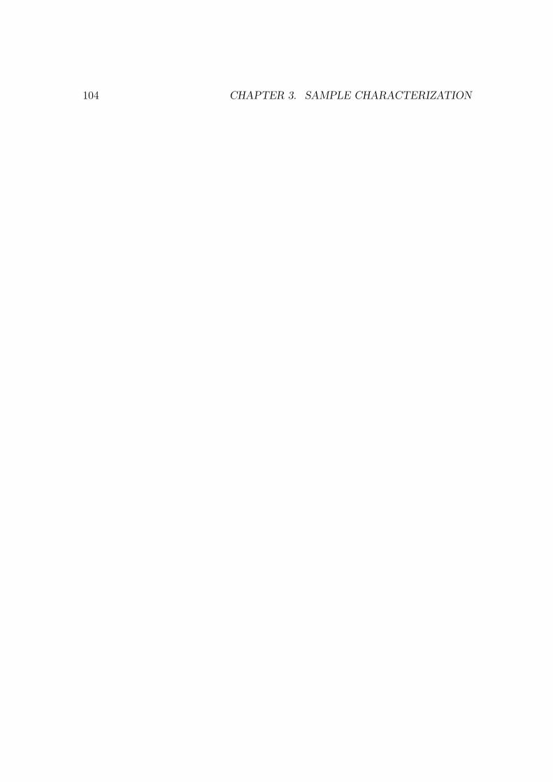
104 CHAPTER 3. SAMPLE CHARACTERIZATION

Chapter 4
Experimental results and
discussion I: ZnSe
Ha-de tomar o pregador uma so materia, ha-de defini-la para que se conheca;
ha-de dividi-la para que se distinga; ha-de prova-la com a Escritura, ha-de
declara-la com a razao, ha-de confirma-la com o exemplo, ha-de amplifica-la
com as causas, com os efeitos, com as circunstancias, com as conveniencias
que se hao-de seguir, com os inconvenientes que se devem evitar.1
Pe. Antonio Vieira
Sermao da Sexagesima
4.1 Introduction
We will now present and discuss the experimental information obtained about the
muonium states in ZnSe, by means of the µSR techniques. As we shall see, the
physics of muonium in ZnSe is very rich, and a vast amount of different phenomena
and interactions is unveiled in temperature-dependent studies. This doesn’t ease
the experimentalist’s work and, in order to disentangle the physics, it is sometimes
1Free translation: ”The preacher shall take a single subject, he shall define it so that it is
known; he shall divide it so that it is distinguishable; he shall prove it with Scripture, he shall
declare it with reason, he shall confirm it with example, he shall amplify it with the causes,
with the effects, with the circumstances, with the conveniences that shall be followed, with the
inconveniences that should be avoided.”

106 CHAPTER 4. ZNSE
necessary to focus in specific parts of the experimental data, which more clearly
display the particularities of a given phenomenon. In the following, we have cho-
sen to present the experimental data in comprehensive sets grouped essentially
according to the experimental subtechnique used. This has the advantage of al-
lowing a broader view first, before moving to particular details, thus facilitating the
interpretation path. Of course, there is physical thought before and after experi-
mental data, and the disadvantage of this presentation scheme is that the identified
processes become somewhat scattered across the chapter. A final synthesis is then
needed and this will be tried in the end of the chapter.
In the course of this work, the samples AA and Ctec have been the most inten-
sively investigated. As seen in the previous chapter, these are the most intrinsic
samples, and so they prove the most adequate for access the ”basic” physics of
muonium/hydrogen in ZnSe. However, even these samples show already some sig-
nificant differences, thus pointing clearly the importance of the interactions with
charge carriers even at this lower extreme doping limit.
We start by presenting high-transverse field (7 T), high time resolution experi-
ences at TRIUMF for the AA and Ctec samples, which allowed the discovery of a
novel muonium state in ZnSe, as well as deep insight into the paramagnetic muo-
nium conversion at low temperatures. Low-transverse field (5− 10 G) experiments
at PSI, presented subsequently, revealed additional dynamics of the diamagnetic
components at about 60 K, which was further explored via final-state analysis
with RF-µSR. These two sets of data, together with the respective interpretation,
constitute the core of this chapter.
We present also additional experimental information, which further supports
the interpretation of the above mentioned data, and whose associated work was
only begun: the spectroscopy at high-temperatures (above room temperature), the
further insight into muonium dynamics by longitudinal field techniques, and the
low-transverse field investigations of the other ZnSe samples, which constitute the
beginning of doping-dependent studies in this material.

4.2. HIGH-TRANSVERSE FIELD SPECTROSCOPY 107
4.2 High-transverse field spectroscopy
4.2.1 Novel deep muonium center in ZnSe
High-field, high time resolution muon spin rotation experiments were performed
using the HITIME spectrometer in the M15 beam-line at TRIUMF, in Vancouver,
Canada. The AA and Ctec samples were investigated. The positron counts in
the four detectors, arranged in a box-like configuration around the sample, were
analysed in a rotating reference frame. A typical time-spectrum (for the AA sam-
ple, T=2 K, at B=7 T) is shown in Fig. 4.1, for a reference frame rotating at
670 MHz. The superposition of two precession frequencies (692.1 MHz and 776.8
MHz, in the case of figure 4.1), is clearly visible in the time spectrum. The corre-
sponding Fourier spectrum is shown in Fig. 4.2, where the lower frequency line is
seen to be significantly broader than the upper line.
Each frequency signal was analysed using an exponentially-damped cosine func-
tion of the form A exp(−λ t) cos(ω t+φ). The fractions of the two states compared
to all muons were calculated from the measured µSR amplitudes assuming that
only half of the weight is expected in the observed ν12 transition, the second half
being contained in the unobserved higher-frequency ν34 transition (please refer to
section 2.3). Instrumental effects that lead to a decrease in the amplitude of the
signals at high-fields are corrected by comparing with the muon precession signal
in silver at the same frequency.
Only the ν12 transition in muonium being observable at high fields, in the
experimentally accessible range, the observation of the two lines indicates either
two distinct muonium centers with different isotropic hyperfine interactions or a
single muonium center with an anisotropic hyperfine interaction. In the latter
situation, the two lines could arise from different angles between the applied field
and the symmetry axis of the hyperfine interaction. We have thus undertaken
an orientation dependence study of these lines, in order to check the anisotropy
hypothesis.

108 CHAPTER 4. ZNSE
Figure 4.1: Time spectrum obtained for ZnSe at T=2.5 K, B=6.9 T. In order to
facilitate the visual inspection, the data are plotted in a rotating reference frame
at 670 MHz. The superposition of the 692.1MHz and 776.8 MHz frequencies is
seen. Note the higher relaxation of the lower frequency. The line is a fit with a
sum of two exponentially-damped cosine functions, as described in the text.
500 600 700 800 900 10000.00
0.01
0.02
0.03
0.04 ZnSe
Mu
Mu
FFT
Powe
r
Frequency (MHz)
Figure 4.2: Fourier transform µSR spectrum of ZnSe (AA sample) at B = 7 T
and T = 2.07 K. Two different states, MuI and MuII are observed. The two lines
correspond to two different isotropic hyperfine interactions, as discussed in the
text.

4.2. HIGH-TRANSVERSE FIELD SPECTROSCOPY 109
Orientation dependence study
In order to check the orientation dependence of the muonia precession lines, we have
used three oriented ZnSe single crystals from the same Ctec batch, cut on the main
crystallographic orientations. In these experiments, the magnetic field was applied
parallel to the [100], [110] and [111] crystallographic orientations, respectively. The
precession frequencies at high-fields for these three samples, together with those for
the AA sample, are summarized in table 4.1. The frequencies are either equal, at
the same applied field, or shift with the characteristic 135.5 MHz/T ratio expected
for purely isotropic centers, for different fields. We thus find that the hyperfine
frequencies are independent, within experimental errors, of the direction between
the applied field and the three major crystallographic directions [100], [110] and
[111].
Sample T (K) TF (T) fI (MHz) fII (MHz) AI (MHz) AII (MHz)
AA 1.9(6) 6.899968 692.1(2) 776.80(8) 3454.6(2) 3282.2(4)
Ctec [111] 5.1(9) 6.899968 692.1(2) 776.82(7) 3454.7(1) 3282.2(4)
Ctec [110] 4.8(12) 6.77999 707.96(19) 792.60(8) 3454.2(2) 3281.9(4)
Ctec [110] 4.86(3) 5.999996 811.9(3) 896.31(8) 3454.3(2) 3282.0(1)
Ctec [100] 2.8(2) 6 812.5 896.25 3454.2(2) 3283.3(4)
Table 4.1: Orientation dependence of the muonium precession frequencies. The
corresponding isotropic part of the hyperfine interaction, as obtained from equation
4.1, is also included.
We therefore conclude that two distinct Mu centers, MuI and MuII, with dif-
ferent isotropic hyperfine interactions are responsible for the observed spectra.
We include in table 4.1 the corresponding hyperfine interactions, obtained from
the following expression, easily derived from table 2.4:
A =2γeγµB
2 − 2ν212 + 2ν12(γe − γµ)B
(γe − γµ)B − 2ν12
(4.1)
110 CHAPTER 4. ZNSE
where the corresponding error σA is given by:
σA = 2
∣∣∣∣A
(γe − γµ)B − 2ν12
+ 1
∣∣∣∣σν12 (4.2)
From the average value of the hyperfine parameters in table 4.1, we estimate the
corresponding values of the hyperfine interactions to be AI = 3282.1(1) MHz and
AII = 3454.4(1) MHz at the lowest measured temperature. These values correspond
to 73.5 % and 77.4 % of the vacuum value, respectively.
From the maximum observed difference of the hyperfine interaction values in
table 4.1 and eqs. 2.40 and 2.39, we may obtain a maximum limit for the value
of a presumed dipolar component D in the hyperfine interaction, obtaining DI <
0.5 MHz and DII < 1.4 MHz.
4.2.2 Temperature dependence of the paramagnetic states:
AA sample
We now address the temperature dependence of the paramagnetic lines, as observed
in these high-field muon spin rotation experiments. We present firstly, in this
section, the results for the AA sample, which allow deeper insight, and leave for
the next section the corresponding results for the Ctec sample.
Figure 4.3 shows the fractions of the two muonium states in the AA sample, as
a function of temperature. Up to 40 K, both states coexist, MuI being nearly twice
as intense as MuII, and the total muonium fraction being 79±1%. Above 40 K,
MuI disappears and the fraction of MuII increases strongly in a narrow temperature
interval. This indicates a conversion of MuI to MuII, the latter being the only state
visible at higher temperatures. The total intensity of visible muonium signals
decreases strongly above the conversion region. This probably is an effect of muon
spin depolarization during the time between implantation and formation of the
final state, since no appreciable change in the diamagnetic signal is observed in the
entire temperature range. The diamagnetic signal strength is extremely small and
consistent with zero diamagnetic fraction arising from the ZnSe sample. This signal
can probably be entirely accounted for by muons stopping outside the sample, at

4.2. HIGH-TRANSVERSE FIELD SPECTROSCOPY 111
all temperatures below 300 K. We shall come back to this point.
The temperature dependence of the depolarization rates λ of the two states can
be seen in Fig. 4.4. The most obvious feature is the strong increase of λ for MuI
between 10 and 40 K. This is attributed to the temperature activated conversion of
state I to state II. The relaxation of MuI is also rather large (about 14 µ s−1) before
the onset of the conversion process perhaps due to a rapid spin fluctuation of MuI.
The relaxation of state MuII is very low and does not change up to approximately
200 K, which includes the region of the conversion of state I to state II. Above
200 K an increase of the depolarization of MuII is seen.
The phases of the signals in each detector are governed by the detector geometry
with respect to the muon spin polarization prior to implantation. However, as was
discussed in chapter 2, additional phase shifts are introduced if the muon exists for
some time in a precursor state before it forms the final configuration. Such phase
shift effects are seen in Fig. 4.5 for MuII as a dip around 50 K and as the gradual
decrease above 100 K.
1 10 1000
25
50Mu (b)
Fracti
on (%
)
T (K)
25
50
75 Mu (a)
Figure 4.3: Fractions of the two muonium states, MuI (a) and MuII (b), observed
for the AA sample at TF 7 T, as a function of temperature. MuI is seen only up
to approximately 40 K.

112 CHAPTER 4. ZNSE
1 10 1000.1
1
Mu (b)
λ (µs
)
T (K)
10
100
Mu (a)
Figure 4.4: Depolarisation rates of the two muonium states, observed for the AA
sample at TF 7 T, as a function of temperature.
1 10 100-200
-160
-120
-80
Mu (b)
Phase
(deg)
T (K)
-125
-100
-75
Mu (a)
Figure 4.5: Phases of the two muonium states, observed for the AA sample at
TF 7 T, as a function of temperature.

4.2. HIGH-TRANSVERSE FIELD SPECTROSCOPY 113
Temperature dependence of the hyperfine interaction
Before discussing the above-mentioned results in more detail, we begin by ad-
dressing the temperature dependence of the hyperfine interaction Aiso for MuII, as
shown in Fig. 4.6. Such data are often modelled assuming an interaction with
long-wavelength phonons which are treated within the Debye model [Pat88].
In this model, the decrease with temperature of the hyperfine interaction is
usually explained by admitting that the atom ground state configuration is mixed
via orbit-lattice interaction with excited configurations of the form ns by a dynamic
phonon-induced field [Sim66], where the lattice vibrations are treated within a
Debye model. The temperature dependence of the hyperfine interaction is proved
to be, in this description:
A = A0
[1− C T 4
∫ θD/T
0
x3
ex − 1dx
](4.3)
where A0 is the hyperfine interaction at T = 0 K, T is the absolute temperature,
θD is the Debye temperature of the material and C is a temperature-independent
parameter.
0 50 100 150 200 250 300
3380
3400
3420
3440
3460
Mu
ZnSe
A (M
Hz)
T (K)
Figure 4.6: Temperature dependence of Aiso of state MuII, observed for the AA
sample at TF 7 T. The red solid line is a fit with a (first-order) Einstein model.
The black line is a fit with a Debye model.

114 CHAPTER 4. ZNSE
In the present case the fit to this model, which is shown in figure 4.6, gives a
Debye temperature of TD = 160 K. The Debye temperature for the ZnSe matrix
from the literature is 275 K [Bir75]. Similar discrepancies in a ratio of roughly 2
to 3, were also found for several other semiconductors [Lic04, Pat88]. However,
the fit with the Debye model is rather poor for the high temperature points in the
current case.
We should note that this model was developped by Simanek and Orbach specif-
ically to explain the temperature dependence of the hyperfine interaction in 3d5,6S paramagnetic ions such as Mn2+. In the case of muonium, we have a 1s1 ground
state configuration, which is admitted to be mixed, in the framework of this model,
with 2s1, 3s1, etc configurations. Perhaps part of the explanation of the failure
lies in the possible mixture with 2p configurations. Or else, the underlying Debye
model does not apply entirely.
A different approach to the problem is to assign the temperature dependence
to a local vibrational mode (e.g. the oscillation of muonium in the potential pro-
vided by the matrix) and assume that the change of the hyperfine interaction is
adequately described by a series on the mean square displacement < u2 >:
A(T ) = a0 + a2 < u2 > + a4 < u4 > + ... (4.4)
Within this harmonic oscillator model, the temperature dependence can be
obtained from a Boltzmann distribution. Admitting, for simplicity, a single vibra-
tional frequency ν (Einstein model), one arrives at the following formula for the
temperature dependent isotropic hyperfine interaction A(T ):
A(T ) = A0 +C1
exp(hν/kT )+
C2
(exp(hν/kT ))2(4.5)
where A0 is the hyperfine interaction at T = 0 K and ν is the single vibration
frequency in an Einstein model. The coupling constants C1 and C2 are assumed
temperature-independent. Eq. 4.5 corresponds to the first three terms of the
formula given in reference [Rod95] and reference [Mor94]. Without the second
order term, a fit with this model, shown in figure 4.6, did not describe well the

4.2. HIGH-TRANSVERSE FIELD SPECTROSCOPY 115
data points at the higher temperatures, indicating a deviation from the simple
proportionality between A and < u2 >.
The fit (solid line in Fig. 4.7) gives an energy hν = 8.0 ± 0.1 meV. Such a low
vibrational energy, if attributed to the oscillation of muonium in the cage, would
correspond to an extremely flat potential.
The limited temperature range for observation of MuI does not allow any de-
tailed determination of the temperature dependence of the respective hyperfine
interaction.
0 100 200 3003350
3375
3400
3425 Mu
A (M
Hz)
T (K)
Figure 4.7: Temperature dependence of Aiso of state MuII, observed for the AA
sample at TF 7 T. The solid line is a fit with an Einstein model, as described in
the text.

116 CHAPTER 4. ZNSE
MuI to MuII conversion
A second important aspect in these high-field experimental data relates to the
conversion of MuI to MuII. We have analysed this aspect with the simple conversion
model presented in chapter 2. There, we found the following expression for the
polarization change ∆P (t), in the case where state I, detected via frequency ωI,
converts to a state II, which is detected via frequency ωII:
∆P (t) = AI exp(−t/τ) cos(ωI t + φI) (4.6)
+AI√
1 + (∆ω τ)2cos(ωII t + φI − tan−1(∆ω τ))
− AI exp(−t/τ)√1 + (∆ω τ)2
cos(ωI t + φI − tan−1(∆ω τ))
where τ is the mean lifetime of the initial state and ∆ω = ωII − ωI > 0. For τ an
Arrhenius ansatz τ = τinf exp(Ea/kT ) was used, with Ea the activation energy. An
acceptable global fit of all data using a unique set of parameters for the conversion
could not be obtained. The increase of the relaxation of MuI and the rise of the
fraction of MuII (Fig. 4.8) are too far separated in temperature to be fitted with
a single activated conversion process. A similar discrepancy was observed for the
conversion of MuI to MuII in CuCl and CuBr [Kie86]. The reason is probably
that in the stage before the actual conversion, local motion of muonium and of the
lattice atoms change dramatically and result in an increase of the spin relaxation.
In Fig. 4.8(b) and Fig. 4.8(c), the solid lines show the fit to the amplitude
and phase of MuII. In the fit we assumed that the amplitudes of MuI and MuII do
not change in the conversion temperature range and that their values are the same
as at low temperatures. This, however, is not completely correct and leads to the
overestimation of the MuII fraction above 60 K in Fig. 4.8(c). From this fit, we
obtain Ea = 17 meV and τinf = 1.1× 10⁻⁴ µs. These values should be considered
as a first approximation for the MuI to MuII transition, since any other dynamic
process involving either state has been left out of this simple model. With the
same fitted parameters as in Fig. 4.8(b) and (c), the solid line in Fig. 4.8(a) is
calculated. The discrepancy indicates again that the conversion process is more
intrincate than assumed in our model. The possible existence of a pre-conversion
dynamics, as discussed above, may justify the difference.

4.2. HIGH-TRANSVERSE FIELD SPECTROSCOPY 117
0 25 50 75 10020406080 Mu (c)
Fracti
on (%
)
T (K)
-110-100-90-80
Mu (b)
Phase
(deg)
0
200Mu (a)
λ (µs
)
Figure 4.8: Relaxation rate of MuI, phase shift of MuII, and fraction of MuII,
observed for the AA sample at TF 7 T, as a function of temperature. The solid
lines are fit curves assuming activated conversion of MuI into MuII, as described in
the text.

118 CHAPTER 4. ZNSE
”Missing fraction”
At low temperatures, ∼ 21% of the muons are not observed in high transverse-
field. Figures 4.3 and 4.8 show that the total muonium fraction, above 60 K
represented by the fraction MuII, decreases with temperature. As pointed out
above, no corresponding change is observed in the diamagnetic fraction. A possible
explanation for the ”missing fraction” is that the donor electrons of ZnSe, which
become activated [Dev67] at around 60 K, cause a depolarization of the muon spin
in a precursor stage during the thermalization process, i.e. in the time between
the implantation and the formation of the final state.
As indicated in Fig. 4.4 and Fig. 4.5, there is a dramatic change in the
relaxation and phase of the MuII signal above about 200 K. Aditionally, in the
same temperature range, up to room temperature, the muonium fraction becomes
temperature independent (fig. 4.3). Above 200 K, donor ionization is essentially
complete and any process that depends critically on conduction electron concen-
tration begins to saturate. We note that a conversion from a precursor stage can
not lead to an increase in the relaxation of the final state. Therefore, the increase
of the depolarization of MuII above 200 K (Fig. 4.4) must be due to a process
acting on MuII directly.
It is also unlikely that the increase of the relaxation is due to the onset of a
conversion of this state to another state since, as we shall see in section 4.5.3,
MuII is observed up to 550 K. This observation is not consistent with an activated
conversion setting in already at 200 K.
Additionally, the observed change in the phase of MuII above 150 K (Fig.4.5) is
not related to the MuI to MuII conversion since that transition has already become
very rapid well below that temperature. These features imply that additional
dynamics are present for both MuII and a precursor state which is not necessarily
MuI. Thus an interaction with conduction electrons might be the cause of the
relaxation and the phase shift must be caused by some process in the precursor
stage. We shall come back to this in section 4.4.

4.2. HIGH-TRANSVERSE FIELD SPECTROSCOPY 119
4.2.3 Temperature dependence of the paramagnetic states:
Ctec sample
We show in figures 4.9 to 4.12 the result of similar temperature dependence stud-
ies in high-field muon-spin rotation experiments, undertaken with the Ctec [100]
sample.
Though the basic characteristics of the two muonium states are the same, as was
already pointed out in table 4.1, these data nevertheless show some enlightening
differences:
(i) as show in figure 4.9, the total muonium fractions observed at the lowest
temperature is now 91(1)% (79(1)% for the AA sample), and the additional fraction
is essentially due to MuI;
(ii) above 25 K, the MuII state is now seen to broaden (fig. 4.10) and its
amplitude to decrease to zero at 60 K (fig. 4.9), whereas the MuI state is no longer
observable due to extreme broadening, as seen in figure 4.10;
(iii) the two states cease to be observed before any significant phase shift ap-
pears, as seen in fig. 4.11.
1 10 1000
25
50Mu (b)
Fracti
on (%
)
T (K)
0
25
50
75
100 Mu (a)
Figure 4.9: Fractions of the two muonium states, MuI (a) and MuII (b), observed
for the Ctec sample at TF 7 T, as a function of temperature. MuI is seen only up
to approximately 20 K and MuII up to 50 K.

120 CHAPTER 4. ZNSE
1 10 1000.1
1
10Mu (b)
λ (µs
)
T (K)
10
100
Mu (a)
Figure 4.10: Depolarisation rates of the two muonium states, observed for the Ctec
sample at TF 7 T, as a function of temperature. The line in (a) is a fit with an
Arrhenius activated function, yielding an activation energy of 6(1) meV.
1 10 100-120
-80
-40
Mu (b)
Phase
(deg)
T (K)
-125
-100
-75
-50
Mu (a)
Figure 4.11: Phases of the two muonium states, observed for the Ctec sample at
TF 7 T, as a function of temperature.

4.2. HIGH-TRANSVERSE FIELD SPECTROSCOPY 121
These features point to the presence of an additional process besides MuI →MuII
conversion. This conversion is still present, and is signed only via the broadening
of the MuI state seen in fig. 4.10, similarly to that observed for the AA sample 4.4.
However, the onset at 25 K of the new process involving MuII and leading to its
disappearance already above 50 K prevents the observation of the characteristic
phase shift in the MuII precession frequency. Also, as seen in fig. 4.12, only a
hint of the the temperature dependence of the hyperfine interaction AII is seen.
Thus, only the increase of the relaxation rate remains as sign of conversion, which
has been fitted to a simple Arrhenius activation, yielding an activation energy of
6(1) meV. This should be compared to the value obtained when fitting the same
process to the corresponding increase in the AA sample (fig. 4.4), where we obtain
an energy of 7(1) meV, much smaller than the 17 meV obtained in the global fit
of fig. 4.8.
From these data, not much can be extracted about the nature of this process,
except that it is related to the greater abundance of charge carriers in the Ctec
sample (please refer to table 3.3 and subsequent comments). This larger concen-
tration of charge carriers in the Ctec sample is apparent in the larger fraction of
muons that capture an electron at low temperatures, as expressed in the total muo-
nium fraction. The reason why only the formation probability of MuI is affected
is however not clear.
0 20 40 60
3440
3460Mu
A (M
Hz)
T (K)
Figure 4.12: Temperature dependence of Aiso of state MuII, observed for the Ctec
sample at TF 7 T. Only a hint of the corresponding decreasewith temperature is
present, before the disappearance of the MuII frequency.

122 CHAPTER 4. ZNSE
4.2.4 Discussion
The high-field muon spin rotation experiments have revealed a new muonium state
in ZnSe at low temperatures, the presence of which accounts for a large portion of
the muon fraction that was missing in previous experiments. The detection of this
state was made possible only in a high time resolution setup, by the application
of a high magnetic field in which the depolarization of the state is sufficiently
slow to allow for its observation. The two states observed here have characteristics
very similar to those reported[Kie86, Sch90, Sch92] for CuCl. In these publications,
after a detailed characterization of the local surroundings of muonium, definite site
assignments were determined via interaction with the abundant nuclear moments,
placing both Mu centers in the tetrahedral cage with Cu nearest neighbors but with
different lattice relaxations and different specific locations and motional properties
for Mu.
A similar situation may exist for both MuI and MuII in ZnSe. By analogy, we
expect both centers to reside in the same region, i.e. in the tetrahedral interstitial
cage surrounded by four nearest neighbor Zn ions. In this case, MuI corresponds
to muonium embedded in the not yet relaxed lattice. It finds potential minima
slightly off the center position and tunnels among the different sites. A muonium
impurity at an off-center location within the tetrahedral cage should have some
anisotropy in its hyperfine interaction. The dynamical effect of tunneling would
average out this anisotropy and could explain the rather large depolarization of
MuI discussed above. In the CuCl analogy, MuII can be assigned to muonium in
the center of the Zn cage after lattice relaxation has occurred in reaction to the
presence of the muon. There is apparently a barrier between the two configurations
which is overcome thermally in the range where the conversion from MuI to MuII
is observed. A separation of singlet and triplet tunneling states for muonium
delocalized over four cation-related sites has also been proposed as an explanation
for such a barrier [Cox87].
Another interpretation of the two signals could be that they correspond to two
different sites, one to muonium in the anion tetrahedral cage and the other to
muonium in the cation tetrahedral cage of ZnSe. In a theoretical paper [VdW93a],

4.2. HIGH-TRANSVERSE FIELD SPECTROSCOPY 123
isotropic hyperfine interactions of 3333 MHz for Mu in the Zn cage (TZn) and of
3248 MHz for Mu in the Se cage (TSe) were predicted, which are remarkably close to
our experimental values. In this second interpretation, MuI would correspond to a
deep-donor state at TSe, where a neutral and a positively charged muonium center
can be located. MuII corresponds in this interpretation to a deep acceptor state at
the TZn site, where a neutral and a negatively charged center can be located.
In the zincblende structured II-VI materials, which have considerable ionic
character in the bonding, the anion cage becomes competitive with the bond-
centered location for both the neutral and positively charged donor states. The
strong evidence here for conversion from MuI to MuII would then imply that the
TZn acceptor site is the more stable location for Mu in ZnSe. This experimental
evidence also implies that, in the two-site model, the site-change transition is faster
than MuI ionization below roughly 50 K. However, if the MuI deep-donor ionization
rate were competitive and increasing rapidly with temperature, then ionization of
MuI prior to conversion to MuII could provide an explanation for the decrease in
MuII amplitude that is observed between 60 and 150 K (Fig.4.3). This is also
consistent with a second exit route from MuI as inferred from the mismatch of the
MuI relaxation results when compared to the fits to the data of Fig. 4.8.
The present experiment confirms that normal muonium at an acceptor site,
here called MuII, is the stable muon configuration in ZnSe. The only other neutral
signal in ZnSe is MuI which converts to MuII. Here, no sign of the shallow effective-
mass donor has been found. Thus ZnSe belongs to the class of semiconductors in
which the shallow donor is absent and instead one or more deep muonium centers
are observed, as is the case for Si or for GaAs [Cho98, Pat88]. These high-field
data provide no clear experimental evidence for ZnSe, as there was for CuCl, on
which to base an independent choice between the two-site and single-site models;
thus, it is not definite at this juncture whether or not a deep donor state is also
observed in addition to the deep acceptor ground state. However, several arguments
favour the single-site model: the MuI relaxation rates, the very close resemblance of
ZnSe to the CuCl system (both from the crystallographical and the ionic character
point of view), as well as the similarity of the respective muonium experimental

124 CHAPTER 4. ZNSE
data, together with the definite assignment of the two Mu signals to the same
T-site cage in CuCl. All these advocate rather strongly in favour of the single-site
interpretation.
4.3 Low-transverse field spectroscopy
The investigation of the above-noted difference among the AA and Ctec samples
was continued at low-transverse-fields at PSI. The AA sample was investigated at
the GPS instrument, with a transverse field of 5 G, and the Ctec [111] sample was
investigated at the DOLLY instrument, with a transverse field of 10 G. Both sam-
ples were implanted with muons polarized in the backward (B) direction, and the
transverse field was applied in the left-right (L-R) direction. As usual, all directions
are referred with respect to the incoming muon momentum. Time histograms were
accumulated in the detectors placed in the forward (F), backward (B), up (U) and
down (D) positions. Again, each histogram was fitted with one or two exponen-
tially damped sinusoidal function with the form A exp(−λt) cos(2πνt + φ). Silver
calibration measurements were used to obtain the instrument maximum asymme-
try. Typical spectrums for the AA and Ctec samples are shown in figs. 4.13 and
4.14.
4.3.1 AA sample
As is eloquently expressed by fig. 4.13, in the AA sample we observe essentially a
paramagnetic fraction, although a marginal diamagnetic fraction is present as well
in the spectra.
We present in figures 4.15 and 4.16 the results for the paramagnetic and dia-
magnetic fractions and relaxations. A very small diamagnetic fraction is observed,
presenting no temperature dependence, and which may be attributed to back-
ground.
At these low-fields, the muonium ν12 and ν23 precession frequencies are inde-
pendent of the hyperfine interaction, and it is therefore not possible to distinguish
the paramagnetic Mu states spectroscopically. However, the observed state is iden-

4.3. LOW-TRANSVERSE FIELD SPECTROSCOPY 125
0.0 0.1 0.2 0.3 0.4-5
0
5ZnSe, AA
Asym
metry
time (µs)
Figure 4.13: Time spectrum obtained for the AA sample, at T=55 K and TF=5 G.
Only the first 400 ns are shown, where a 8 MHz oscilation, due to muonium, is
visible. The line is a fit with a lorentzian damped 8 MHz oscillation.
0 2 4 6 8 10-10
-5
0
5
10ZnSe, Ctec
Asym
metry
time (µs)
Figure 4.14: Time spectrum obtained for the Ctec sample, at T=55 K and
TF=10 G. Unlike what is observed for the AA sample (fig. 4.13), the muonium
oscillation is no longer visible at this temperature, instead a significant 0.14 MHz
diamagnetic frequency is seen. The line is a fit with an unrelaxed 0.14 MHz oscil-
lation.

126 CHAPTER 4. ZNSE
0 100 200 3000
5
ZnSe, AA
diamagnetic
Fracti
on (%
)
Temperature (K)
0
10
20
30paramagnetic
Figure 4.15: Paramagnetic (MuII) and diamagnetic fractions, observed for the AA
sample at TF 5 G = 0.5 mT, as a function of temperature.
10 100
0.0
0.5diamagnetic
λ (µs
)
Temperature (K)
0
10
20paramagneticZnSe, AA
Figure 4.16: Depolarisation rates of the paramagnetic (MuII) and diamagnetic
fractions, observed for the AA sample at TF 5 G = 0.5 mT, as a function of
temperature.

4.3. LOW-TRANSVERSE FIELD SPECTROSCOPY 127
tified with MuII, since the high relaxation of the MuI state, as seen under the 7 T
field, does not allow its direct observation in the lower resolution setup at PSI.
Also, the experimentally observed Mu precession frequency presents no tempera-
ture dependence, as expected at low fields where the ν12 and ν23 frequencies are
independent of the hyperfine interaction, as discussed in section 2.3.
We note, in fig. 4.15, the difference in the paramagnetic MuII fraction at the
lowest temperature ( 17%, vs. 25% at 7 T, see fig. 4.3). This may be due to
the repolarization of part of the missing fraction. We note that this can not be
attributed to the field dependence of the converted asymmetry, since we expect it
to be smaller in high fields.
The 50 K peak observed in the high transverse field data (fig. 4.3), is here
observed at the same temperature and is again identified with MuI →MuII con-
version. The decrease of the MuII fraction above 50 K is also present, with no
apparent impact in the diamagnetic fraction. The corresponding relaxations are
shown in fig. 4.16. Despite no significant changes are observed in the respective
temperature dependence, a quite broad relaxation of the MuII state is observed.
Again, the dynamical process above 200 K makes itself visible via a slight
reincrease of the MuII fraction, which amounts to c. 12% of the total muon spin
polarization at 300 K.
It looks therefore that these low-field data bring no new information with re-
spect to the high-field data at TRIUMF and are, in some sense, redundant. How-
ever, three types of reasons impose the need to consider them here:
(i) the contrast with the Ctec low-field TF data, shown in the next section, and
which have, unlike these data, new information;
(ii) the spectroscopical investigations of the processes undergoing at higher
temperatures (above room temperature) can only be done at PSI; these data thus
provide us with a coherent set of data from liquid-He temperature, to the highest
temperature attainable at PSI; we leave the presentation of these high temperature
investigations to a later moment;
(iii) finally, these data confirm our previous high-field data and interpretation.

128 CHAPTER 4. ZNSE
4.3.2 Ctec sample
We present in figures 4.17, 4.18, 4.19 and 4.20 the results for the corresponding low
field (TF10G) muon spin rotation measurements of the Ctec sample, undertaken at
the DOLLY instrument at PSI. Unlike the case for the AA sample, we now observe
a significant diamagnetic fraction (see fig. 4.14), peaking at about 60 K (fig. 4.17).
This had not been observed in the 7 T measurements, which stopped, for this
sample, at 45 K. The diamagnetic fraction is seen to increase with temperature
from 3% at 30 K up to 25% at 65 K. This increase matches the corresponding
decrease in the paramagnetic fraction, identified once again with MuII. Of note,
the low-temperature MuII fraction now observed is equal to the one seen in the
high-field experiments (cf. fig. 4.9), indicating that the low-temperature dynamical
process leading to the missing fraction in the AA sample is now absent.
Other signatures of conversion from MuII to the diamagnetic fraction, in the 30
- 60 K region, include the relaxation increase in the MuII signal (figure 4.18) and
the pronounced phase-shift in the diamagnetic signal (figure 4.19).
Above 60 K, another process sets in, leading to the disappearance of the dia-
magnetic fraction, and an increase of the diamagnetic relaxation is observed (fig.
4.20), though it is obscured by the almost complete disappearance of this fraction
above 100 K.
Discussion
The data just presented for the Ctec sample at TF 10 G clearly display signs of
conversion of the paramagnetic fraction (presumably, and most reasonably, MuII)
to a diamagnetic fraction. This occurs as a thermally activated process from about
30 K to 60 K and, as the difference among the two samples indiciates, is observed
mostly in the sample with higher concentration of conduction electrons.
As in the conversion of MuI to MuII, discussed in the previous section, the con-
version of the paramagnetic fraction to the diamagnetic fraction is visible through
the increase of relaxation of the converting state, and as an asymmetry increase
and phase-shift of the converted state.

4.3. LOW-TRANSVERSE FIELD SPECTROSCOPY 129
10 1000
10
20diamagnetic
Fracti
on (%
)
Temperature (K)
0
10
20
30 paramagneticZnSe, Ctec
Figure 4.17: Paramagnetic (MuII) and diamagnetic fractions, observed for the
Ctec sample at TF 10 G = 1 mT, as a function of temperature. The line in
the diamagnetic fraction graph is a fit assuming an activated electron capture, as
discussed in the text. The line in the paramagnetic fraction graph is a simulation
for the corresponding variation of the paramagnetic fraction.
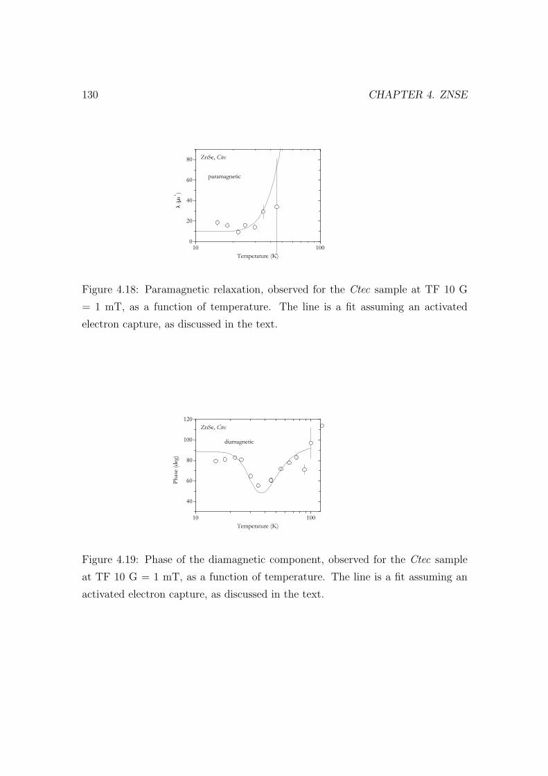
130 CHAPTER 4. ZNSE
10 1000
20
40
60
80
paramagnetic
ZnSe, Ctec
λ (µs
)
Temperature (K)
Figure 4.18: Paramagnetic relaxation, observed for the Ctec sample at TF 10 G
= 1 mT, as a function of temperature. The line is a fit assuming an activated
electron capture, as discussed in the text.
10 100
40
60
80
100
120
diamagneticZnSe, Ctec
Phase
(deg)
Temperature (K)
Figure 4.19: Phase of the diamagnetic component, observed for the Ctec sample
at TF 10 G = 1 mT, as a function of temperature. The line is a fit assuming an
activated electron capture, as discussed in the text.
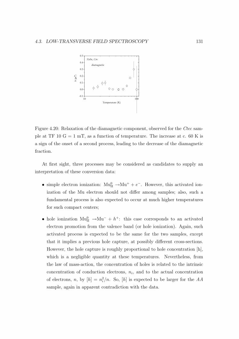
4.3. LOW-TRANSVERSE FIELD SPECTROSCOPY 131
10 100-0.1
0.0
0.1
0.2
0.3
0.4
0.5
diamagneticZnSe, Ctec
λ (µs
)
Temperature (K)
Figure 4.20: Relaxation of the diamagnetic component, observed for the Ctec sam-
ple at TF 10 G = 1 mT, as a function of temperature. The increase at c. 60 K is
a sign of the onset of a second process, leading to the decrease of the diamagnetic
fraction.
At first sight, three processes may be considered as candidates to supply an
interpretation of these conversion data:
• simple electron ionization: Mu0II →Mu+ + e−. However, this activated ion-
ization of the Mu electron should not differ among samples; also, such a
fundamental process is also expected to occur at much higher temperatures
for such compact centers;
• hole ionization Mu0II →Mu− + h+: this case corresponds to an activated
electron promotion from the valence band (or hole ionization). Again, such
activated process is expected to be the same for the two samples, except
that it implies a previous hole capture, at possibly different cross-sections.
However, the hole capture is roughly proportional to hole concentration [h],
which is a negligible quantity at these temperatures. Nevertheless, from
the law of mass-action, the concentration of holes is related to the intrinsic
concentration of conduction electrons, ni, and to the actual concentration
of electrons, n, by [h] = n2i /n. So, [h] is expected to be larger for the AA
sample, again in apparent contradiction with the data.

132 CHAPTER 4. ZNSE
• second electron capture Mu0II + e− →Mu−, which seems to be the most
physically sensible process and which readily makes the data understandable:
– this implies the capture of a second electron occurring after the ioniza-
tion of the donors of the material, possibly after the muon thermaliza-
tion;
– it seems likely that this delayed capture may be even more delayed if
the concentration of donors is smaller, and this might explain why the
diamagnetic fraction is not observed in the AA sample; the second elec-
tron takes too long, and/or this capture is preceded by spin fluctuations
that depolarize the muon spin and lead to a (much smaller) decrease of
the paramagnetic amplitude, without the corresponding increase of the
diamagnetic amplitude.
– at the lowest temperatures, as pointed out in the preceding section, only
a small percentage of the muons implanted in the Ctec sample manage
to capture the second electron; the process becomes more important as
donors are ionized and more conduction electrons become available.
Analysis of second electron capture by MuII
We have analysed the relevant parameters (paramagnetic relaxation, diamagnetic
fraction, diamagnetic phase) with the same model applied to the MuI to MuII
conversion (eq. 4.6).
In the Mu0II + e− →Mu− model, the lifetime τ of the MuII state is the inverse
of the capture rate νc of the second electron. In the simplest approach, νc is
expected to be proportional to the concentration n of conduction electrons and to
the respective velocity ve:
νc = σc ve n (4.7)
where σ is the cross section for the capture and the mean thermal velocity is given
by [Rei65]2:
2Cf. eq. 7.10.16 of the cited reference.

4.3. LOW-TRANSVERSE FIELD SPECTROSCOPY 133
ve =
√3kT
m∗e
(4.8)
The temperature dependence of the concentration of conduction electrons in the
conduction band, for a compensated n-type semiconductor with Na compensating
acceptors and Nd donors with spin degeneracy β (usually taken to be β = 1/2) at
the single donor ionization energy Ed, is given by [Bla62]3:
n(n + Na)
Nd −Na − n= β Nc exp
(−Ed
kT
)(4.9)
where Nc is the effective density of states in the conduction band and is given
by[Bla62]4:
Nc = 2
(m∗
ekT
2πh2
)3/2
(4.10)
and m∗e = 0.16 m0 is the electron effective mass in this compound [Mad82].
This formula can be further simplified at low temperatures, assuming Nd >>
n >> Na:
n = n∞ exp
(− Ed
2kT
)(4.11)
where
n∞ =√
β Nc Nd (4.12)
An exponential, Arrhenius-like, dependence for the capture rate 4.7 is therefore
expected in this approximation, with an activation energy which is about half of
the donor energy Ed:
νc = σc ve n∞ exp
(− Ed
2kT
)= ν∞c exp
(− Ed
2kT
)(4.13)
In the final analysis, we have used this exponential approximation, and fixed
the donor energy to 30 meV (i.e., the Arrhenius activation energy to 15 meV),
3Cf. p. 138, in the cited reference.4Cf. p. 80, in the cited reference.
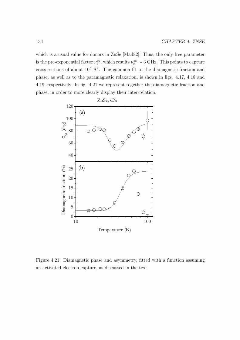
134 CHAPTER 4. ZNSE
which is a usual value for donors in ZnSe [Mad82]. Thus, the only free parameter
is the pre-exponential factor ν∞c , which results ν∞c ∼ 3 GHz. This points to capture
cross-sections of about 105 A2. The common fit to the diamagnetic fraction and
phase, as well as to the paramagnetic relaxation, is shown in figs. 4.17, 4.18 and
4.19, respectively. In fig. 4.21 we represent together the diamagnetic fraction and
phase, in order to more clearly display their inter-relation.
10 10005
10152025 (b)
ZnSe, Ctec
Diam
agneti
c frac
tion (
%)
Temperature (K)
40
60
80
100
120(a)
φ
(deg)
Figure 4.21: Diamagnetic phase and asymmetry, fitted with a function assuming
an activated electron capture, as discussed in the text.

4.4. FINAL-STATE ANALYSIS EXPERIMENTS 135
4.4 Final-state analysis experiments
The low-field experiments presented above prompted us to investigate more thor-
oughly the diamagnetic fraction in ZnSe. From eq. 4.6, it is clear that the ampli-
tude of the diamagnetic final fraction is expected to vary with 1/√
1 + (∆ω τ)2,
from which we may expect a rough variation with the inverse of the applied mag-
netic field. This effect, which corresponds to the dephasing of the converted state,
explains why the diamagnetic fraction is seen only in low applied fields.
The final state can be best investigated by means of the muon spin resonance
technique presented in Chapter 2, which, being in its essence a longitudinal field
technique, is free from the dephasing problems.
We have thus undertaken final state analysis of the diamagnetic fraction in the
Ctec and the AA samples, by means of RF-µSR measurements. These measure-
ments were performed at ISIS, with the RF setup. The flypast setup was used
in order to reduce background. Polyethene calibration measurements were done
in order to obtain the maximum experimental asymmetry, thus allowing to ob-
tain the fraction of muons thermalizing in the diamagnetic state in the sample
under investigation. The corresponding temperature dependences of the measured
diamagentic fractions are represented in figs. 4.22 and 4.23, respectively.
These measurements were further complemented in the same sample with muon
spin resonance measurements of the paramagnetic MuII fractions state, performed
by Prof. Roger Lichti and Dr. Kim Chow with the microwave setup at TRIUMF.
In these microwave measurements, no calibration of the maximum asymmetry was
done, which prevents to determine the observed muonium fractions. However,
at the lowest temperature, the fraction of the MuII state observed in the muon
spin resonance measurements should not be inferior to the fraction observed in
high-transverse field (unlike the situation at temperatures above the conversion to
diamagnetic, where the relaxation of MuII may disguise the total integral asym-
metry). We have thus taken the asymmetry of the lowest temperature point in
the microwave measurements to correspond to the MuII fraction observed at the
lowest temperature in TF 7T. This has been used as our ”calibration” and we
have thus estimated the corresponding MuII fractions. It should be stressed that

136 CHAPTER 4. ZNSE
10 1000
20
40
60
80
100
Diam
agneti
c frac
tion (
%)
T (K)
Figure 4.22: Temperature dependence of the diamagnetic fraction in the Ctec
sample, as measured by muon spin resonance methods at ISIS.
10 1000
20
40
60
80
100
Diam
agneti
c frac
tion (
%)
T (K)
Figure 4.23: Temperature dependence of the diamagnetic fraction in the AA sam-
ple, as measured by muon spin resonance methods at ISIS.

4.4. FINAL-STATE ANALYSIS EXPERIMENTS 137
10 1000
20
40
60
80
100
Param
agneti
c Mu
fracti
on (%
)
T (K)
Figure 4.24: Temperature dependence of the paramagnetic MuII fraction in the
Ctec sample, as measured by muon spin resonance methods at TRIUMF.
10 1000
20
40
60
80
100
Param
agneti
c Mu
fracti
on (%
)
T (K)
Figure 4.25: Temperature dependence of the paramagnetic MuII fraction in the
AA sample, as measured by the muon spin resonance method at TRIUMF.

138 CHAPTER 4. ZNSE
these correspond to a lower limit, admitting the entire MuII asymmetry is observed
in the resonance measurements at the lowest temperature (8 K). The estimated
paramagnetic MuII fractions, are represented in figs. 4.24 and 4.25 for the Ctec
and the AA sample, respectively.
4.4.1 Discussion
We start the discussion of these results by the most informative data of the Ctec
sample, and afterwards reason about the data of the AA sample.
For the Ctec sample, the diamagnetic RF experiments proved most successfull
and full diamagnetic fraction is observed at 60 K, soon followed by a rapid decay
up to 100 K. This increase of the diamagnetic fraction appears in relation to the
observed decrease of the paramagnetic MuII fraction, which is observed in the
microwave experiments. Also, it correlates with the relaxation of the MuII fraction,
observed in the spectroscopic studies (cf. figs. 4.10 and 4.18).
All this is readily understood if we admit that the growth of the diamagnetic
fraction is due to the delayed capture of a second electron, available via ionization
of the donors in the material, as discussed for the low-transverse field data.
Regarding the low temperature diamagnetic fraction (9.9%), which is not ob-
served in the spectroscopic 7 T data, it may be argued that it too corresponds to
slowly-formed Mu−, unobserved at high-fields due to dephasing. If it corresponded
to muons thermalizing directly as Mu+, there seems not to be any reason for it
being invisible at 7 T.
In the AA sample, with its lower concentration of conduction electrons, this
delayed capture of a second electron by MuII is almost suppressed, and instead the
effect of the ionization of donors and subsequent increase of conduction electrons
is a depolarization of the muon spin, eventually by spin-exchange dynamics before
thermalization. This causes a decrease of the observed MuII fraction both by purely
spectroscopic means (as was already pointed out in the discussion of the missing
fraction of the 7 T data) and by muon-spin-resonance methods.
These muon spin resonance experiments allow us to clearly establish a third
process in the Ctec sample, corresponding to the disappearance of the diamag-

4.4. FINAL-STATE ANALYSIS EXPERIMENTS 139
netic fraction in the 60-100 K region which, as we shall see below, may be related
to the increase of the paramagnetic MuII fraction, observed at somewhat higher
temperatures in the microwave experiments.
The disappearance of the diamagnetic fraction above 60 K, together with the
late reappearance of the paramagnetic fraction can be thought of as either:
(a) hole capture: Mu− + h+ → Mu0
(b) (second) electron ionization: Mu− → Mu0 + e−
Regarding (a), this process is again dependent on the hole concentration, pre-
sumably negligible at these temperatures. Also, it is reasonable that the second
electron may be somewhat loosely bound, meaning a not very intense potential
well at the muon site. We therefore prefer the second electron ionization as the
best candidate model to explain the decrease of the diamagnetic fraction observed
in the RF experiments at the Ctec sample, although we have no clear experimental
evidence in favour of process (b), or against process (a).
Capture and Release model for T≥60K
We now present a very simple model that tries to describe the essential features in
figs. 4.22 and 4.24, while trying to extract some essential quantitative information,
particularly the most relevant ionization energy. We start with a capture and
ionization model trying to grasp the details in the T≥60 K region.
We therefore assume that, above T≥60 K, both capture and release of a second
electron occur:
Mu0II + e− −→
νc
Mu−II (4.14)
Mu−II −→νi
Mu0II + e− (4.15)
where the capture rate νc and the ionization rate νi are assumed to be given by:
νc = neveσc (4.16)

140 CHAPTER 4. ZNSE
νi = ν0i exp
(− Ei
kT
)(4.17)
As done previously, when the expression 4.16 was first presented (eq. 4.7), we
have used its simpler form 4.13:
νc = σc ve n∞ exp
(− Ed
2kT
)= ν∞c exp
(− Ed
2kT
)(4.18)
where σc is the cross-section for electron capture and the mean thermal velocity of
conduction electrons is given by
ve =
√3kT
m∗e
= 16 857.69
[ms−1
√K
]√T (4.19)
the electron effective mass in the bottom of the conduction band of ZnSe being
m∗e = 0.16 m0.
Regarding the ionization rate 4.17, we assume it to be essentially a thermally
activated process, governed by the activation energy Ei. In our interpretation,
this corresponds to the energy required to promote an electron from the doubly
occupied MuII 1s orbital to the bottom of the conduction band. This parameter is
thus identified, in this interpretation, with the depth of the (-/0)T conversion level
below the conduction band.
From equations 4.14 and 4.15, the paramagnetic and diamagnetic fractions fp
and fd may be derived, taking into account that a fraction converting at rate ν
decreases exponentially with exp(−νt). The following set of coupled equations can
therefore be written:
fp(t) = f 0p e−νc t + νi
∞∫
0
fd(τ) e−νc (t−τ) dτ (4.20)
fd(t) = f 0d e−νit + νc
∞∫
0
fp(τ) e−νi(t−τ) dτ (4.21)
where f 0p and f 0
d are the initial paramagnetic and diamagnetic fractions, respec-
tively.

4.4. FINAL-STATE ANALYSIS EXPERIMENTS 141
In a muon spin resonance experiment, the time-averaged fractions are bound
to be observed. The time average f of a fraction f(t) is:
f = νµ
∞∫
0
f(t) e−νµ tdt (4.22)
However, the observation of the fractions in a muon spin resonance experi-
ment may be obscured in the presence of dynamical phenomena leading to further
depolarization of the states under research, such as those discussed in chapter 2.
Unlike the capture stage, evidence for the existence of such aditional dynamical
phenomena is abundant for the ionization stage:
(i) the reincrease of the paramagnetic fraction in the Ctec sample occurs higher
in temperature than the concomitant decrease in the diamagnetic fraction;
(ii) in the AA sample, the corresponding variations occur primarily in the para-
magnetic fraction; as pointed out before already, this is taken as a sign of spin
dynamics taking place in the presence of a concentration of conduction electrons
small enough to almost completely suppress electron capture;
We have included these dynamical phenomena assuming it leads to further
depolarization of the states. This has been included as an ad hoc depolarization
rate ν1 in eq. 4.22:
f = νµ
∞∫
0
f(t) e−(νµ+ν1) tdt (4.23)
Furthermore, we have taken ν1 with a Chow’s dependence (cf. eq. 2.65):
ν1 =νc νi ω
20
2(νc + νi)(ν2c + ω2
0 + (2π(γe + γµ)B))2(4.24)
where (γe + γµ) = 28127.873 MHz T−1, ω0 = 2π × 3454.26 Mrad s−1 and B =
0.1955 T for the diamagnetic data and B = 0.8746 T for the paramagnetic data.
The resulting average fractions become:
fp = f 0p
νµ
νc + νµ + ν1
+ fdνi
νc + ν1 + νµ
(4.25)

142 CHAPTER 4. ZNSE
fd = f 0d
νµ
νi + νµ + ν1
+ fpνc
νi + νµ + ν1
(4.26)
and, after solving this linear system of two equations and two unknowns, we get:
fp =νµ
νµ + ν1
f 0p (νi + νµ + ν1) + f 0
d νi
νµ + νi + ν1 + νc
(4.27)
fd =νµ
νµ + ν1
f 0d (νc + νµ + ν1) + f 0
p νc
νµ + νi + ν1 + νc
(4.28)
Capture model including MuI
The above model may be further improved by including the third known process
involving the muonium states in ZnSe, which is the conversion between the para-
magnetic states MuI and MuII:
Mu0I −−−→
νI/II
Mu0II (4.29)
where the conversion rate νI/II is again taken as
νI/II = ν0I/II exp
(−EI/II
kT
)(4.30)
The time-dependent fractions of the paramagnetic and diamagnetic states now
become:
fI(t) = f 0I e−νI/II t (4.31)
fII(t) = f 0II e−νct + νI/II
∞∫
0
fI(τ) e−νc(t−τ) dτ + νi
∞∫
0
fd(τ) e−νc (t−τ) dτ (4.32)
fd(t) = f 0d + νc
∞∫
0
fII(τ) dτ (4.33)

4.4. FINAL-STATE ANALYSIS EXPERIMENTS 143
We note that the conversion from MuI to MuII is already finished by 40 K, well
before the ionization of Mu−II sets in, so that these two extreme processes may be
thought not to coexist. During the conversion of MuI to MuII, we may thus set
νi = 0. Consequently the relaxation arising from the ionization/capture process
is negligible, and ν1 = 0 as well. The average fraction is given by the simpler eq.
4.22.
The average fractions, with the assumptions above, become:
fI = f 0I
νµ
νI/II + νµ
(4.34)
fII = f 0II
νµ
νc + νµ
+ fI
νI/II
νc + νµ
(4.35)
fd = f 0d + fII
νc
νµ
(4.36)
and, after the solution of the above system of three coupled equations is:
fI = f 0I
νµ
νI/II + νµ
(4.37)
fII = f 0II
νµ
νµ + νc
+ f 0I
νµ νI/II
(νI/II + νµ)(νµ + νc)(4.38)
fd = f 0II
νc
νc + νµ
+ f 0I
νc νI/II
(νI/II + νµ)(νµ + νc)+ f 0
d (4.39)
Analysis with the model
We have used the above models for the analysis of muon spin resonance data of the
Ctec sample. We started by the low-temperature (up to 60 K) data shown in figs.
4.22 and 4.24, which were analysed with eqs. 4.39 and 4.38, respectively. Despite
the success of the fit to the diamagnetic data, the model does not describe accu-
rately the paramagnetic data, as can be seen in fig. 4.26, where total paramagnetic

144 CHAPTER 4. ZNSE
fraction observed in the high-transverse (7 T) field is also shown for comparison. In
the fit, we allowed the MuI to MuII conversion parameters to vary with respect to
the previous parameters obtained from the high-transverse field data and obtained
EI/II = 13(1) meV and ρI/II = 0.09(5)×103 MHz. Regarding the capture parame-
ters, the fit to the diamagnetic fraction improves very much if we allow the capture
energy to vary. We obtain ν∞c = 2.6(3) GHz and Ec = 20.8(4) meV, slightly below
the expected value for the donor energies in ZnSe, which are measured between 26
and 30 meV [Mad82].
We have fitted the high-temperature part separately with eqs. 4.28 and 4.27.
We obtained, for the ionization parameters, ν0i = 5(2)×1013 MHz and Ei = 178(2)
meV. Though the fit to the diamagnetic fraction works well by fixing the capture
parameters from the low-temperature part, yielding similar values, the fit to the
paramagnetic fraction works better by allowing the capture parameters to be let
free, converging to new values (ν∞c = 5.4(9)×109 MHz, Ec = 69(1) meV). We take
this as a sign of the frailty of the model, more than of any substantial evidence
for an actual change of the capture process. The result of the corresponding fit is
shown in fig. 4.27.
A visual summary of the overall analysis is shown in fig. 4.28.
AA sample
It is clear from the discussion above that the model we used for analysing the muon
spin resonance data of the Ctec sample is not expected to describe adequately
the corresponding AA data. Here, the capture of the second electron is strongly
suppressed due to the lower concentration of conduction electrons, and this seems
to be substituted by temperature-dependent spin-dynamics. We have nevertheless
used eq. 4.39 to fit the muon spin resonance data for the diamagnetic fraction,
by fixing the parameters obtained for the Ctec sample, except the concentration
dependent parameter ν∞c . We obtained ν∞c = 0.45(2) MHz (to be compared with
ν∞c = 2.6(3) GHz for the Ctec sample), which is a very sensible lower value. The
resulting fit is shown in fig. 4.29.

4.4. FINAL-STATE ANALYSIS EXPERIMENTS 145
10 1000
20
40
60
80
100
RF fra
ction
(%)
T (K)
Figure 4.26: Diamagnetic (white circles) fraction and paramagnetic MuII (black
circles) for the Ctec sample, as obtained by muon-spin-resonance methods. The
half-black circles represent the total paramagnetic fraction observed in the spec-
troscopic 7 T experiments. Solid lines are fits with eqs. 4.39 and 4.38, respectively,
using common parameters for the muonium interconversion and second electron
capture. Dashed lines are simulations with the same capture parameters, but as-
suming the entire paramagnetic fraction is due to MuII, which allows to evidence
the contribution of each process.

146 CHAPTER 4. ZNSE
10 1000
20
40
60
80
100
RF fra
ction
(%)
T (K)
Figure 4.27: Diamagnetic (white circles) fraction and paramagnetic MuII (black
circles) for the Ctec sample, as obtained by muon-spin-resonance methods. The
half-black circles represent the total paramagnetic fraction observed in the spec-
troscopic 7 T experiments. Solid lines are fits with eqs. 4.28 and 4.27, respectively,
using common parameters for the muonium ionization and second electron capture.
Dashed lines are simulations with the same capture and ionization parameters, but
seting the ad hoc relaxation ν1 (eq. 4.24) to zero.

4.4. FINAL-STATE ANALYSIS EXPERIMENTS 147
10 1000
20
40
60
80
100
RF fra
ction
(%)
T (K)
Figure 4.28: Diamagnetic (white circles) fraction and paramagnetic MuII (black
circles) for the Ctec sample, as obtained by muon-spin-resonance methods. The
half-black circles represent the total paramagnetic fraction observed in the spec-
troscopic 7 T experiments. Solid and dashed lines are the superposition of the
corresponding fits and simulations presented in figs. 4.26 and 4.27.
10 1000
20
40
60
80
100
Diam
agneti
c frac
tion (
%)
T (K)
Figure 4.29: Diamagnetic fraction for the AA sample, as obtained by muon-spin-
resonance methods. The line is a fit with eq. 4.39, as explained in the text.

148 CHAPTER 4. ZNSE
4.5 Further experimental information
We now present additional experimental information gathered in the course of this
work and which, despite its somewhat fragmentary nature, allows further signifi-
cant insight either into the processes already discussed in the previous sections, or
into new processes.
4.5.1 Probing Mu dynamics with LF
From the discussion of the muon spin resonance data, it is clear that our model,
despite describing already the essential features of the muon spin resonance data
for the Ctec sample, requires further refining in order to allow a confident and
accurate determination of the relevant energy levels, which correspond o a major
objective in this investigation, as discussed in chapter 1. A problem which was
already partially adressed is that of the muonium spin dynamics in the course of
the relevant electronic processes. As mentioned in chapter 2, a way of probing this
spin dynamics is by verifying the field dependence of the average polarization and
of the muon spin relaxation in longitudinal field geometry.
We have only begun to adress this question experimentally, by investigating the
Ctec sample longitudinal fields at ISIS (EMU), in the temperature interval between
60 K and 100 K (corresponding to the range where the process we identify with
ionization occurs). As usual in these measurements, a silver calibration was done
in the entire field range (up to 4500 G), in order to obtain the (field-dependent)
maximum asymmetry Amax.
A typical time spectrum is shown in fig. 4.30, where a relaxation is ob-
served in the initial instants of the asymmetry. The time-averaged polarization
τ−1µ
∫ tmax
0A(t) exp(−t/τµ)dt/Amax, as a function of applied longitudinal field, is
shown for four temperatures in fig. 4.31. In fig. 4.32, we depict the corresponding
relaxations, obtained by fitting a two-component function A1 + A2 exp(−λt).
As expected, we observe in fig. 4.31 the typical field-dependent polarization
behaviour in the presence of dynamical phenomena (as discussed in the context of
eq. 2.59). However, the average polarization is seen to decrease pronouncedly with

4.5. FURTHER EXPERIMENTAL INFORMATION 149
0 2 4 6 8 10-10
-5
0
5
10 ZnSe, Ctec
Asym
metry
time (µs)
Figure 4.30: Muon spin relaxation time spectrum, obtained for the Ctec sample,
at T=80 K, under an applied longitudinal field LF=10 G
1 10 100 10000
20
40
60
80
100
65 K 70 K 80 K 100 K
ZnSe, Ctec
Avera
ge po
lariza
tion (
%)
LF (G)
Figure 4.31: Longitudinal-field-quenching (repolarization) curves, obtained for the
Ctec sample, for four distinct temperatures. Solid lines are fits with eq. 2.59.

150 CHAPTER 4. ZNSE
increasing temperature, relating to the increasing relaxation. The repolarization
curves are adequately fit with eq. 2.59: values for the charge-exchange rate ν about
107 MHz and for the duration of the charge-exchange cycle τ in the microsecond
range are obtained, with a large error.
Fits to the relaxation data in fig. 4.32, with the refined Chow’s model for the
1/T1 relaxation (eq. 2.65), allow to further extract the paramagnetic to diamag-
netic conversion rate λ0d and its converse λd0. In the interpretation used for the
muon spin resonance data in the previous section, λ0d corresponds to the capture
rate νc and λd0 corresponds to the ionization rate νi. The results of these fits are
shown in fig. 4.33, together with the corresponding values predicted by the para-
meters obtained by fitting eq. 4.13 to the RF data. The obtained correlation is
quite sucessfull. These data therefore suggest that a thorough longitudinal field
study may allow to improve the estimation of the conversion levels, by using direct
information about the temperature dependent conversion rates.
1E-4 1E-3 0.01 0.1 1
0.1
1
10 65 K 70 K 80 KZnSe, Ctec
λ (µs
)
LF (T)
Figure 4.32: Relaxation rates corresponding to the repolarization curves in fig.
4.31. For 100 K, the relaxations are much close to the high limit of the experimen-
tally accessible range and are not included in the plot. Solid lines are fits with eq.
2.65.

4.5. FURTHER EXPERIMENTAL INFORMATION 151
60 70 801
10
ν
Temperature (K)
1
10
100
ν
Figure 4.33: Ionization rate νi and capture rate νc, obtained from longitudinal-field
(LF) measurements and from RF-µSR measurements. Black circles represent the
values resulting from eqs. 4.13 and 4.17, with the parameters extracted with the
analysis to the muon-spin resonance (RF) data. White circles represent the values
extracted from the muon spin relaxation (LF) measurements (fig. 4.32), by fitting
with the Chow’s formula (eq. 2.65).
152 CHAPTER 4. ZNSE
4.5.2 Development of doping-dependent studies
We extended the previous spectroscopical studies to the more strongly doped sam-
ples presented in Chapter 3: the chemical-vapour-grown (CVT) samples, delib-
erately or undeliberately doped with iodine (CVT:I and CVTu, respectively), as
well as a Ctec sample annealed in Zn vapour, in order to reduce compensation by
vacancies (Ctec:Zn). These studies, which still have a preliminary character, have
been done at low transverse fields (10 G), at PSI.
We depict the temperature dependence of the diamagnetic fraction observed in
all samples in fig. 4.34. For clarity, the AA sample is excluded, the corresponding
diamagnetic fraction being residual (see fig. 4.15).
We note that, for the Ctec:Zn sample, the peak in the diamagnetic fraction
attributed to delayed capture of a second electron is slightly higher both in height
(26% vs. previous 23%) and in temperature (75 K vs. 65 K). We take this fraction
increase as a sign of the expected larger capture rate. As mentioned in chapter 3,
this sample was annealed in zinc, which reduces the concentration of zinc vacancies
and the compensation associated with these defects. The concentration of free
electrons is thus expected to increase, favouring the capture of a second electron
by muonium and therefore increasing the diamagnetic fraction.
However, the most remarkable effect is observed for the low-temperature dia-
magnetic fraction observed in the CVT-grown samples, which is already much
larger from the lowest temperatures, without even peaking. This is expected, in
our interpretation, for these higher concentrations of conduction electrons, which
correspondingly increase the capture rate.
Such high concentrations of free carriers and of impurities/defects, eventually
leading even to impurity-band conduction, trigger or enhance processes whose pres-
ence is just unveiled by the current experiments. Particularly, it should be noted
that no paramagnetic fraction is observed for the CVT-grown samples, in these
TF 10 G experiments. A paramagnetic fraction (amounting to 30% at 45 K) is
observed in the Ctec:Zn sample (not in the CVT-grown samples), representing
already a significant difference with respect to what was observed before the an-
nealing (cf. fig. 4.17). Even more strikingly, the diamagnetic fraction of the CVT:I

4.5. FURTHER EXPERIMENTAL INFORMATION 153
sample is observed to grow above 100 K to nearly 100%, and a similar trend is
observed in the CVTu sample. These two samples also present an increasing relax-
ation of the diamagnetic fraction above 250 K (fig. 4.35). The presence of a second
relaxing diamagnetic component in the CVT:I sample seems to occur (amounting
to 4% at room temperature, with a relaxation rate around 7 µs−1). No relaxation
is observed in the Ctec:Zn sample.
It is possible that the above mentioned features above 200 K correspond to
the high-free-carrier-concentration limit of the corresponding dynamical features
observed for the more intrinsic samples, as discussed in the previous sections. Or
they may be the sign of entirely new processes setting in only at high concentrations
of conduction electrons. Processes such as muon and muonium diffusion, trapping
at impurities/defects can not neither easily be ruled out or confirmed, attending
to the low-density of nuclear moments in ZnSe, as discussed in section 2.5.
An adequate modelling for these phenomena is still lacking, and its interrelation
is poorly understood. These data therefore constitute more a departure than an
arrival point.
Most significantly, we take the mentioned correlation of the observed diamag-
netic fraction at the lowest temperatures with the concentration of free carriers as
a very positive qualitative confirmation of the delayed second capture model.
Aditionally, we should mention that we also undertook very brief measurements
at an hydrogenated piece of a Ctec sample from the same batch. This piece was
annealed in H2 atmosphere (16 atm, 500o C, for 22 h, Cf. [Hei59, Mol54]), and no
mass difference was found before and after the treatment, thus giving a maximum
introduced concentration of [H] < 5 × 1019 cm−3). Hydrogen being amphoteric
in ZnSe, it is expected to decrease the concentration of conduction electrons, and
thus also decreasing the delayed formation of Mu−. In the three experimental
points obtained (5 K, 55 K and 300 K, at low-transverse field - 10 G - in the GPS
instrument, PSI), the diamagnetic fraction was observed to drop below 6%, which
we again take as further confirmation of our interpretation.

154 CHAPTER 4. ZNSE
10 1000
20
40
60
80
100 CVT:I CVTu Ctec:Zn Ctec
ZnSe
Temperature (K)
Diam
agneti
c Frac
tion (
%)
Figure 4.34: Temperature dependence of the diamagnetic fraction observed by
muon spin rotation measurements (TF=10 G) for the Ctec, Ctec:Zn, CVTu and
CVT:I samples (see chapter 3 for sample reference).
0 100 200 3000.0
0.3
0.6
0.9 CVT:I CVTu
λ (µs
)
Temperature (K)
Figure 4.35: Temperature dependence of the diamagnetic relaxation observed by
muon spin rotation measurements (TF=10 G) for the CVTu and CVT:I samples.
No significant relaxation is observed for the Ctec and Ctec:Zn samples (see chapter
3 for sample reference).

4.5. FURTHER EXPERIMENTAL INFORMATION 155
4.5.3 High temperature investigations
As we have seen, the paramagnetic fraction is observed by muon-spin resonance
methods in the Ctec and AA samples and is observed spectroscopically in the AA
sample up to room temperature. The question of its thermal stability is a most
relevant one with respect to the determination of the hydrogen levels in the band
gap of this material.
However, as is abundantly expressed in the previous section, this determination
is hindered by the coexistence of a profusion of phenomena affecting the muon spin.
We have nevertheless started investigations above room temperature in the Ctec
and AA samples, in the two possible experimental directions:
(i) probing spectroscopically the thermal stability of the paramagnetic fraction
which is observed at room temperature in the AA sample; this requires the inves-
tigation at low transverse fields at PSI, where it is possible to extend spectroscopic
studies up to 700 K;
(ii) final state analysis, by the muon spin resonance technique, of the diamag-
netic fraction observed in the Ctec and AA samples; this is possible at ISIS, where
a high-temperature RF setup has been recently developped.
Low transverse field spectroscopy
We have therefore extended the previous low-transverse field (5 G) investigations
of the paramagnetic fraction of the AA sample up to 700 K. This is observed to
disappear completely at 600 K, a concomitant reappearance of the diamagnetic
fraction being observed as well (fig. 4.36). These data suggest that the MuII state
might not be at all stable above 600 K.

156 CHAPTER 4. ZNSE
0 200 400 6000
5
ZnSe, AA
diamagnetic
Fracti
on (%
)
Temperature (K)
0
10
20
30paramagnetic
Figure 4.36: Temperature dependence of the paramagnetic and diamagnetic frac-
tions observed by muon spin rotation measurements (TF=5 G), at PSI. White
circles denote cryostat measurements and white triangles denote furnace measure-
ments.

4.5. FURTHER EXPERIMENTAL INFORMATION 157
Final state analysis
The temperature dependence of the diamagnetic fraction was further detailed by
the muon spin resonance technique, using the high-temperature RF setup at ISIS.
Both RF measurements and usual TF20G measurements were done. We present
the corresponding results for the Ctec sample and the AA sample in figs. 4.37 and
4.38, respectively.
The most simple process able to explain these data, at the light of the previous
interpretation, is of course muonium ionization by promotion of the muonium
electron to the conduction band:
Mu0 → Mu+ + e− (4.40)
These data, together with the current state of the interpretation, are not enough
to clearly establish process 4.40. Another simple process that might explain the
increase of the diamagnetic fraction at these temperatures is hole ionization:
Mu0 → Mu− + h+ (4.41)
However, this seems less reasonable, as it implies formation again at high tem-
peratures of the Mu− state, which is most likely to become thermally unstable
already at 60 K. Nevertheless, the possibility that muonium behaves as a recom-
bination centre, as is the case if process 4.41 occurs, has been considered in order
to explain high-temperature data for GaAs [Cho96] and, more recently, for InSb
[Sto06].
Despite the case for muonium ionization (process 4.40) still needing further
experimental work in order to be established in more firm grounds, we have nev-
ertheless tried to analyse the RF data with an electron capture and release model
similar to the one used for the low temperature data.

158 CHAPTER 4. ZNSE
300 400 500 600 700 8000
25
50
75
100 RF TF20G
Diam
agneti
c Frac
tion (
%)
T (K)
ZnSe, Ctec
Figure 4.37: Diamagnetic fraction, observed for the Ctec sample above room tem-
perature, at ISIS, by muon spin rotation measurements (black circles) and by muon
spin resonance measurements (white circles).
300 400 500 600 700 8000
25
50
75
100 RF TF20G
Diam
agneti
c Frac
tion (
%)
T (K)
ZnSe, AA
Figure 4.38: Diamagnetic fraction, observed for the Ctec sample above room tem-
perature, at ISIS, by muon spin rotation measurements (black circles) and by muon
spin resonance measurements (white circles).

4.5. FURTHER EXPERIMENTAL INFORMATION 159
We therefore assume that the increase of the diamagnetic fraction is essentially
due to electron loss to the conduction band at a rate νi, with possible recapture at
rate νc, i.e.:
Mu+II + e− −→
νc
Mu0II (4.42)
Mu0II −→
νi
Mu+II + e− (4.43)
where the corresponding rates are simply taken to have an Arrhenius-type temper-
ature dependence:
νi = ν0i exp
(− Ei
kT
)(4.44)
νc = ν0c exp
(−Ec
kT
)(4.45)
Similarly to eqs. 4.28 and 4.27, the paramagnetic and diamagnetic fractions fp
and fd can be expressed as:
fp(t) = f 0p e−νit + νc
∞∫
0
fd(τ) e−νi(t−τ) dτ (4.46)
fd(t) = f 0d e−νct + νi
∞∫
0
fp(τ) e−νc(t−τ) dτ (4.47)
The corresponding average fraction f , relevant in muon spin resonance mea-
surements, is once more given by:
f = νµ
∞∫
0
f(t) e−(νµ+ν1) tdt (4.48)
where we have introduced again an ad hoc relaxation ν1 given by eq. 4.24. We
thus obtain:
fp = f 0p
νµ
νi + νµ + ν1
+ fdνc
νi + νµ + ν1
(4.49)

160 CHAPTER 4. ZNSE
fd = f 0d
νµ
νc + νµ + ν1
+ fpνi
νc + νµ + ν1
(4.50)
and the solution of the above system of equations is:
fp =νµ
νµ + ν1
f 0p (νc + νµ + ν1) + f 0
d νc
νµ + νc + νi + ν1
(4.51)
fd =νµ
νµ + ν1
f 0d (νi + νµ + ν1) + f 0
p νi
νµ + νc + νi + ν1
(4.52)
We have fitted both RF data-sets with this model, imposing the same value for
the ”ionization” energy Ei and fixing the capture energy to the value obtained in
section 4.4.1 (Ec = 69 meV). We obtain values in the order of n0i = 1× 1030 MHz
and Ei = 1 eV. For the capture prefactors, which were let free, we obtain n0c =
6× 10²¹ MHz for the Ctec sample and n0c = 1× 10¹⁰ MHz for the AA sample. The
resulting fit is shown in fig. 4.39.
200 300 400 500 600 700 800 9000
20406080
100
RF di
amagn
etic f
ractio
n (%)
Temperature (K)
Figure 4.39: High-temperature diamagnetic fractions observed in the Ctec and AA
samples by muon spin resonance. Solid lines are a fit as described in the text. The
dashed line is a simulation of the diamagnetic fraction for the AA sample setting
the ad hoc relaxation ν1 to zero (no significant difference is found when doing the
same for the Ctec fraction).

4.6. CONCLUSIVE REMARKS 161
4.6 Conclusive remarks
We now summarize the essential results obtained for ZnSe in the course of this
investigation. Some of these results have already been included in a number of
publications, either dedicated specifically to ZnSe [Vil05b], either dedicated to
the more general context of muonium/hydrogen in II-VI semiconductors [Cox03a,
Lic06, Vil06, Vil07a, Wei03a, Wei03b]. Other aspects are presented here for the
first time, the respective publication in peer-reviewed journals being currently (Jan-
uary/2007) in preparation [Vil07b].
At low temperatures, in high-precision transverse-field measurements, two muo-
nium states MuI and MuII are observed with isotropic hyperfine parameters of AI
= 3282.63±0.51 MHz and AII = 3454.26±0.02 MHz (74 % and 77 % of the vac-
uum value, respectively). State I is thermally unstable and converts to state II at
approximately 40 K. State II is stable up to 600 K. We assign MuII to the cation
interstitial tetrahedral site and discuss the possibility that MuI may correspond
either to muonium at the same site but in the unrelaxed lattice or to the anion
interstitial tetrahedral site. The temperature dependence of the hyperfine interac-
tion of MuII was fitted with a local vibrational model giving an oscillator energy
of approximately 8 meV.
Low-transverse field measurements, performed in a sample with a slightly higher
concentration of free-electrons allowed to identify a conversion of the MuII state
to a diamagnetic fraction, in the temperature range 20-60 K, which we assign
to delayed capture of a second electron forming Mu−II. MuII is thus acting as a
trapping center, although this designation should be taken with care, given the
thermodynamical instability of this center.
This diamagnetic fraction was further investigated by muon-spin-resonance,
and it was shown to become thermally unstable above 60 K, and a recovery of the
paramagnetic MuII fraction was observed as well in related muon-spin-resonance
measurements. We identify this process with ionization of the second electron of
Mu−II to the conduction band. Analysis with a simple model yields an ionization
energy of 178 meV, which in this interpretation corresponds to the distance of the
acceptor level -/0 to the bottom of the conduction band. However, this process is

162 CHAPTER 4. ZNSE
obscured by the existence of dynamical processes of the muon spin, which remain
largely unexplored and poorly understood. Thus, alternative interpretations to
ionization to the conduction band (such as hole capture) can not be entirely ruled
out.
Muon spin relaxation methods, together with the extension to the investigation
of doped samples, may allow deeper insight to these dynamical phenomena, thus
providing more firm grounds to the level -/0 acceptor level assignment.
Muon spin spectroscopy and resonance measurements above room temperature
unveil the thermal instability of the paramagnetic fraction above 400 K, together
with a concomitant increase of the diamagnetic fraction. We tentatively assign
this process to MuII ionization to the conduction band, in which case the +/0 level
should lie c. 1 eV below the conduction band bottom. As the caveats expressed
above clarify, this should be understood as a new resarch route to be pursued in
the future.

Chapter 5
Experimental results and
discussion II: ZnS and ZnTe
Nem sempre sou igual no que digo e escrevo.
Mudo, mas nao mudo muito.
A cor das flores nao e a mesma ao sol
De que quando uma nuvem passa
Ou quando entra a noite
E as flores sao cor da sombra.
Mas quem olha bem ve que sao as mesmas flores.1
Alberto Caeiro
O guardador de rebanhos, XXIX
We now present the experimental data obtained for the other two II-VI zinc
chalcogenides ZnS and ZnTe. As discussed in Chapter 1, these two compounds
also present the characteristic doping unipolarity, ZnS growing as n-type and ZnTe
growing as p-type. At the light of what we learned already of the role of charge
carriers in ZnSe, we thus expect to observe identical phenomena in ZnS to those
of ZnSe, but not in ZnTe. This is effectively the case, as we shall now see.
1Free translation: ”I’m not always the same in what I say and write. I change, but I do not
change much. The colour of the flowers is not the same under the sun than when a cloud is going
by or when the night sets in and the flowers have the colour of the shadow. But he who looks
attentively sees the same flowers.”
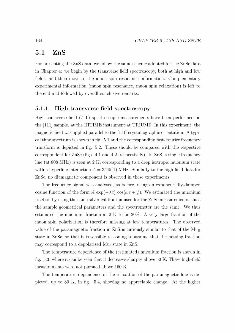
164 CHAPTER 5. ZNS AND ZNTE
5.1 ZnS
For presenting the ZnS data, we follow the same scheme adopted for the ZnSe data
in Chapter 4: we begin by the transverse field spectroscopy, both at high and low
fields, and then move to the muon spin resonance information. Complementary
experimental information (muon spin resonance, muon spin relaxation) is left to
the end and followed by overall conclusive remarks.
5.1.1 High transverse field spectroscopy
High-transverse field (7 T) spectroscopic measurements have been performed on
the [111] sample, at the HITIME instrument at TRIUMF. In this experiment, the
magnetic field was applied parallel to the [111] crystallographic orientation. A typi-
cal time spectrum is shown in fig. 5.1 and the corresponding fast-Fourier frequency
transform is depicted in fig. 5.2. These should be compared with the respective
correspondent for ZnSe (figs. 4.1 and 4.2, respectively). In ZnS, a single frequency
line (at 808 MHz) is seen at 2 K, corresponding to a deep isotropic muonium state
with a hyperfine interaction A = 3545(1) MHz. Similarly to the high-field data for
ZnSe, no diamagnetic component is observed in these experiments.
The frequency signal was analysed, as before, using an exponentially-damped
cosine function of the form A exp(−λ t) cos(ω t + φ). We estimated the muonium
fraction by using the same silver calibration used for the ZnSe measurements, since
the sample geometrical parameters and the spectrometer are the same. We thus
estimated the muonium fraction at 2 K to be 20%. A very large fraction of the
muon spin polarization is therefore missing at low temperatures. The observed
value of the paramagnetic fraction in ZnS is curiously similar to that of the MuII
state in ZnSe, so that it is sensible reasoning to assume that the missing fraction
may correspond to a depolarized MuI state in ZnS.
The temperature dependence of the (estimated) muonium fraction is shown in
fig. 5.3, where it can be seen that it decreases sharply above 50 K. These high-field
measurements were not pursued above 160 K.
The temperature dependence of the relaxation of the paramagnetic line is de-
picted, up to 80 K, in fig. 5.4, showing no appreciable change. At the higher

5.1. ZNS 165
Figure 5.1: Time spectrum obtained for ZnS at T=3 K, B=7 T. In order to facilitate
the visual inspection, the data are plotted in a rotating reference frame at 807 MHz.
A single precession line at 808 MHz is seen.
500 600 700 800 900 10000.00
0.02
0.04
0.06
0.08
FFT p
ower
Frequency (MHz)
Figure 5.2: Fourier transform µSR spectrum of ZnS, at B=7 T and T=2 K. Only
one line at 808 MHz, corresponding to a single isotropic Mu state, is observed.

166 CHAPTER 5. ZNS AND ZNTE
0 50 100 1500
5
10
15
20
25
Fraction
(%)
Temperature (K)
Figure 5.3: Temperature dependence of the (estimated) paramagnetic fraction in
ZnS, at TF=7 T. The paramagnetic state becomes negligible above 100 K.
0 20 40 60 800.0
0.1
0.2
0.3
0.4
λ (µs
)
Temperature (K)
Figure 5.4: Temperature dependence of the relaxation of the paramagnetic com-
ponent, observed in transverse field 7 T experiments. No significant variation is
observed.

5.1. ZNS 167
measured temperatures, due to the low asymmetry, it is impossible to extract
sensible values for the relaxation λ and the frequency ω. We can not therefore
establish any eventual increase of the relaxation above 80 K, due to the low value
of the paramagnetic asymmetry.
A temperature decrease of the paramagnetic frequency with temperature, as
noted for the MuII state in ZnSe (fig. 4.6), is observed here as well. In fig. 5.5
we plot the corresponding temperature dependence of the isotropic hyperfine in-
teraction Aiso (obtained with eq. 4.1). This has been analysed with both models
presented in chapter 4. Assuming an interaction with long-wavelength phonons,
treated within the Debye model [Pat88] (eq. 4.3), we obtain a Debye temperature
of 225 K, again in a rough 2 to 3 ratio to the known Debye temperature in ZnS
(350 K, as quoted in ref. [Bir75]). If we instead assume the temperature depen-
dence to arise from a local vibrational mode, treated within an Einstein model (eq.
4.5), we obtain for the vibrational energy hν = 13.3 ± 0.1 meV, where it is suffi-
cient to use eq. 4.5 up to first order. The obtained vibrational energy, similarly to
the result obtained for the Debye temperature, is correspondingly larger than the
8 meV obtained for the ZnSe case. Unlike the ZnSe case, both models adequately
describe the experimental data in the entire measured temperature range.
0 50 100 1503530
3535
3540
3545
3550
A
Temperature (K)Figure 5.5: Temperature dependence of the isotropic hyperfine interaction Aiso in
ZnS, observed in TF=7 T. The line is a fit with a model assuming interaction of
the muonium atom with long-wavelength phonons treated within a Debye model,
as described in the text. A fit with an Einstein model looks similar and is equally
successful in describing these data.

168 CHAPTER 5. ZNS AND ZNTE
5.1.2 Low transverse field spectroscopy
We have investigated the same sample at low transverse fields (15 G), at the
DOLLY instrument at PSI. The temperature dependence from liquid-helium tem-
perature up to room temperature was investigated. The same basic features found
for the ZnSe samples are visible, as we will now present and discuss.
A paramagnetic fraction is observed, amounting to c. 29% at 2 K, and the
diamagnetic fraction at the same temperature is 3%. These two fractions are
observed up to room temperature, with varying amplitude, relaxation (for the
paramagnetic fraction only) and phase (for the diamagnetic fraction only).
In fig. 5.6 we present the temperature dependence of the diamagnetic and
paramagnetic fractions. The paramagnetic fraction is depicted only up to 80 K,
where it is seen to decrease to c. 22%. Above this temperature, the paramagnetic
fraction seems to remain constant at least up to 210 K, and was fixed, in this
temperature range, to a constant value in the analysis in order to reduce the
uncertainty of the correlated parameters.
Similarly to what was observed for the ZnSe Ctec sample, we observe for ZnS
a modest increase of the diamagnetic fraction with increasing temperature from
40 K to 70 K (fig. 5.6), a significant phase-shift of this fraction being observed
as well (fig. 5.7). A concomitant increase of the relaxation of the paramagnetic
fraction is also present (fig. 5.8). Above 200 K, the diamagnetic fraction is found
to decrease again, and this is possibly followed by an increase of the paramagnetic
fraction (not represented in fig. 5.6, due to very significant uncertainty) and the
respective relaxation.
The above-cited features somehow mimic those seen in ZnSe (figs. 4.17, 4.19
and 4.18), and we therefore make use of the same interpretation scheme developped
in chapter 4, taking the under-100 K phenomena to correspond to the capture of
a second electron by the paramagnetic Mu state and the above-200 K features to
correspond to the ionization of this second electron to the conduction band. We
leave a more quantitative analysis to the next section.

5.1. ZNS 169
10 1000
5
10 (b) diamagnetic
Fracti
ons (%
)
Temperature (K)
0
10
20
30
(a) paramagnetic
Figure 5.6: Temperature dependence of the paramagnetic (a) and diamagnetic (b)
fraction in ZnS, as seen in TF 15 G experiments. The paramagnetic fraction is
observed up to room temperature; its value on the fits to the time spectra was
fixed up to 210 K, and is represented by a dashed line.

170 CHAPTER 5. ZNS AND ZNTE
10 100-60
-50
-40
-30
-20
-10 diamagnetic
Diam
agneti
c phas
e (deg
)
Temperature (K)
Figure 5.7: Phase of the diamagnetic fraction, as observed in temperature depen-
dent studies under an applied transverse field of 15 G.
10 1000
5
10
15paramagnetic
λ (µs
)
Temperature (K)
Figure 5.8: Temperature dependence of the relaxation of the paramagnetic com-
ponent, observed at TF=15 G.

5.1. ZNS 171
5.1.3 Final-state analysis of the diamagnetic fraction
The product of a conversion reaction such as Mu0 + e− −→ Mu− is affected by
dephasing in usual transverse-field measurements, as discussed in chapter 4, and
the analysis of the final-state is best done by muon-spin resonance experiments.
We have undertaken, as for ZnSe, muon spin resonance experiments on the
diamagnetic fraction of ZnS. These were done with the RF setup with flypast
at ISIS, and complemented with calibration measurements on polyethene. The
temperature dependence of the resulting diamagnetic fraction is depicted in fig.
5.9, where again a clear recovery up to nearly 100% is observed at c. 90 K. This
has been analysed with the following equation, which results directly from eq. 4.39
in the case of the capture of the second electron occuring for a single paramagnetic
species:
fd = f 0p
νc
νc + νµ
+ f 0d (5.1)
The limiting equation 5.1 follows directly from eq. 4.39 with the trivial limit
f 0I = 0 (and the total identification fp = fII). However, it follows as well as the
limiting case for extremely fast conversion from MuI to MuII (i.e. νI/II >> νc), in
which case we have f 0p = f 0
I + f 0II instead. We find the latter a more convincing
description of the underlying physics. The resulting fit with eq. 5.1 to the data
of fig. 5.9 yields ν∞c = 19(3) MHz and Ec = 17(1) meV (where f 0p was fixed to
79%, corresponding to the complement to 100% of the low temperature value of
the diamagnetic fraction). The activation energy compares favourably with known
donor energies in ZnS (c. 14 meV [Mad82]) and the pre-exponential factor is
intermediate between the values found for the ZnSe AA and Ctec samples.
In fig. 5.9, a significant decrease of the diamagnetic fraction is observed only
above 180 K. This was analysed with eq. 4.28, assuming it corresponds to the
ionization of the muonium’s second electron to the conduction band, as discussed in
chapter 4. The capture parameters were fixed to the values obtained in the previous
fit to the low temperature capture. We obtain, for the ionization parameters,
ν0i = 8(6) × 105 MHz and Ei = 249(17) meV. The resulting fit is shown in fig.
5.10, where it can be seen to describe the experimental data only in the interval
180− 280 K, besides the fixed capture part in the range 30− 70 K.

172 CHAPTER 5. ZNS AND ZNTE
1 10 1000
20
40
60
80
100
Fracti
on (%
)
T (K)
Figure 5.9: Temperature dependence of the diamagnetic fraction in ZnS, as mea-
sured by muon spin resonance methods at ISIS. The line is a fit with eq. 5.1.
1 10 1000
20
40
60
80
100
Fracti
on (%
)
Temperature (K)
Figure 5.10: Temperature dependence of the diamagnetic fraction in ZnS, as mea-
sured by muon spin resonance methods at ISIS. The line is a fit with eq. 4.28, as
described in the text.

5.1. ZNS 173
5.1.4 Probing Mu dynamics with LF
As mentioned previously, measurements in longitudinal field geometry may pro-
vide further insight into the muon-spin dynamics, either by the longitudinal field
quenching repolarization curves, either by the field dependence of the asymmetry
relaxation. We have only begun these studies at ZnS, obtaining the field depen-
dence of the average polarization and of the asymmetry relaxation at 13 K, in
measurements performed at ISIS. These are represented, respectively, in figs. 5.11
and 5.12. In fig. 5.11 we include as well a tentative fit with equation 2.59 (yielding
ν = 1.22(1)×107 MHz and τ = 0.331(3) µs−1). Of course, at this low temperature,
this model is not expected to be adequate to describe the expected MuI to MuII
conversion. Most likely, the apparent step in the low-field points of fig. 5.11 is
now associated with the corresponding decrease observed for the relaxation in fig.
5.12. In this last figure, we include as well a fit with equation 2.65 (where we find
λ0d = 2.2(3) × 106 MHz and λd0 = 8(2) × 103 MHz), where the above caveats
equally apply. These data can nevertheless provide useful hints for the pursuit of
this research path.
1 10 100 10000.0
0.2
0.4
0.6
0.8
1.0ZnS 13.5 K
Avera
ge po
lariza
tion
LF (G)
Figure 5.11: Longitudinal-field-quenching (repolarization) curve, obtained for ZnS
at 13 K. The line is a fit with eq. 2.59 to the points above 80 G.

174 CHAPTER 5. ZNS AND ZNTE
1 10 100 10000.0
0.1
0.2
0.3
0.4
0.5ZnS 13.5 K
λ (µs
)
LF (G)
Figure 5.12: Relaxation rate corresponding to the repolarization curve in fig. 5.11.
The line is a fit with equation 2.65.
5.2 ZnTe
In chapter 1, we have seen that ZnTe contrasts with ZnSe and ZnS, growing nat-
urally p-type and being difficult to dope n-type. Such fundamental difference is
bound to provide substantial differences in the muonium experimental data and
interpretation. In this compound no neutral muonium state was observed to date
[Pat88].
5.2.1 Spectroscopic measurements
Search for spectroscopic evidence of muonium
ZnTe was investigated at TRIUMF using the high-magnetic field capabilities. Both
a high-purity powder and a monocrystalline sample ([110] orientation) were inves-
tigated: two high-statistics points (2.5 K and 100 K) were taken for the pow-
der sample at a transverse field of 5 T; five high-statistics points were taken at
selected temperatures from 5 K to room temperature for the single crystal, at
7 T. In all cases, the only spectroscopic is that of a diamagnetic component,

5.2. ZNTE 175
with temperature-dependent amplitude. Still searching for paramagnetic muo-
nium signs, high-statistics measurements were taken as well at PSI (2 K, 50 K and
100 K), with low-transverse fields (20 G), again revealing nothing but a diamag-
netic component. This diamagnetic component was subsequently investigated at
the GPS instrument at PSI, for the [110] crystal, in the 2− 300 K range.
Temperature dependence of the diamagnetic fraction
A typical asymmetry time spectrum for ZnTe is shown in Fig. 5.13. Maximum
obtainable asymmetry is, for this instrument, Amax = 23.1%, as determined by
measurements on silver. Figure 5.13 informs us that most of the asymmetry is not
seen in ZnTe, constituting a missing fraction.
0 1 2 3 4 5-3-2-101234
Asym
metry
Time (µs)
Figure 5.13: Asymmetry time spectrum obtained for a monocrystalline ZnTe sam-
ple on an applied transverse field TF=20 G, at T=2 K, TF=20 G. Only a diamag-
netic precession is observed.

176 CHAPTER 5. ZNS AND ZNTE
The observed asymmetry oscillations correspond to the Larmor precession of
the muon spin at the given applied field, with a gyromagnetic ratio corresponding
to diamagnetic muonium. These spectra were fitted with a simple cosine function,
for all temperatures, since no relaxation was observed:
A(t) = A0 cos (2πfL + φ0) (5.2)
where A0 is the asymmetry, fL the Larmor frequency and φ0 the phase parameter.
The temperature dependence of this diamagnetic fraction was followed from 2 K
to 300K under a transverse field of 20 G. The observed diamagnetic fraction, as
obtained from fits after normalizing to the maximum asymmetry, is depicted in Fig.
5.14. The diamagnetic fraction is seen to decrease from the lowest temperature to
50 K, and afterwards increasing from 100 K up, not reaching yet a plateau at room
temperature, keeping to values less than 22%. Thus, even at 300 K, c. 80% of the
muons polarization is not seen, constituting a missing fraction. We also observe
variations of the phase of the asymmetry oscillations above 50 K, which are plotted
in Fig. 5.15.
Discussion
We first concentrate on the rise of the diamagnetic fraction from 100 K up to
room temperature. The existence of a phase shift of the diamagnetic asymmetry
oscillations denotes that this fraction is not formed promptly, and that between
the time of muon implantation and the diamagnetic fraction formation, the muon
spin is subject to interactions which are strong enough to induce the spin rotation,
causing the observed angular shift. These interactions do not destroy completely
the muon polarization, which is afterwards detected, suggesting that the delay
should not exceed the nanosecond range. From the value of the shift, one may
therefore estimate the strength of the interaction, which points to a gyromagnetic
ratio of the order of GHz/T.2 Deep muonium states present gyromagnetic ratia
with this order of magnitude, which suggests that a rather strong interaction is
2An angular shift of φ = 60o = π/3 rad, occurring within ∆t = 1 ns, in the presence of a
magnetic field of B = 20 G corresponds to a gyromagnetic ratio γ = φ/ (2π∆tB) = 83 GHz/T.

5.2. ZNTE 177
0 50 100 150 200 250 3000
5
10
15
20
ZnTe
Diam
agneti
c Frac
tion (
%)
T (K)
Figure 5.14: Temperature dependence of the diamagnetic fraction on ZnTe, ob-
served under an applied transverse magnetic field of 20 G.
0 50 100 150 200 250 300-70-60-50-40-30-20-10
0102030
Ph
ase (d
eg)
T (K)
ZnTe
Figure 5.15: Phase of the diamagnetic asymmetry oscillations, as a function of
temperature. The applied transverse magnetic field is 20 G.

178 CHAPTER 5. ZNS AND ZNTE
involved in this case as well. Evidence of such deep state is bound to show up in
longitudinal field repolarization measurements, as will be seen below.
One must also consider that the phase shift appears already above 50 K, at a
temperature below the associated rise of the diamagnetic fraction at 100 K. This
is also a sign of delayed formation. The diamagnetic fraction is hence expected to
be growing before 100 K, the result of the growth not being visible in transverse
field geometry due to dephasing of the muon’s polarization. If this is the case, such
diamagnetic fraction shall appear in RF-µSR measurements, and this is effectively
the case, as we shall see.
Thus, the rise of the diamagnetic fraction from 100 K up, being the result of
delayed formation, is observed only at temperatures high enough for the muon-
polarisation dephasing to be negligible. The actual rise of the fraction occurs
already at somewhat lower temperatures. Holes becoming mobile at about 100 K
in ZnTe, suggests that as the paramagnetic muonium atom has a chance of meeting
a hole, recombination occurs, by occupation of the non-occupied valence band state
by the muonium electron. This process can not occur before acceptors ionization,
since the muonium atom is expected to thermalize at an intrinsic environment, and
the probability to be stopped near a localized hole is negligible. In this model, the
muonium atom is behaving as a compensating (deep) donor.
The behaviour of the diamagnetic fraction below 50 K is most probably related
to muon spin interactions in the precursor stage before thermalization. These
processes, which lead to the missing fraction as well, are still not clearly identified.
5.2.2 Final-state analysis of the diamagnetic fraction
The above results prompted us to investigate the diamagnetic fraction by means
of the final-state analysis allowed by RF-µSR (see section 2.6.4). The RF-µSR
capabilities at ISIS were used. The same Crystec [110] sample used at PSI was
investigated with this technique. The sample was mounted on a mylar flypast
sample holder. The RF frequency was set to 23 MHz (resonance expected at
LF = 1697 G, for the diamagnetic state) and the power to 114W, and a temperature
scan was carried out from 2 K to 300 K. A polyethene sample with the same shape

5.2. ZNTE 179
of the ZnTe single crystal was used for calibration of the maximum RF average
asymmetry at resonance.
0 50 100 150 200 250 300 3500
20
40
60
80
100
PSI TF ISIS RF
ZnTe
Diam
agneti
c Frac
tion (
%)
T (K)
Figure 5.16: Diamagnetic fraction in ZnTe as seen by RF-µSR (open circles) and
usual TF-µSR (closed circles). The line is a fit with the model described in the
text, with Ea = 89± 9 meV, Na = (8± 83)× 1017 cm−3, σ = (90± 5)× 10−7 A2,
pd0 = 4.9± 0.4%. The donor concentration parameter was fixed to Nd = 2.8× 10¹³
cm−3, and the initial paramagnetic fraction p00 was forced to be p0
0 = 100%− pd0.

180 CHAPTER 5. ZNS AND ZNTE
Discussion
The diamagnetic fraction in ZnTe, as determined from the RF temperature scan
is depicted in Fig. 5.16, together with the corresponding diamagnetic fraction
observed in the TF studies performed at PSI. The RF data clearly demonstrate
that the missing fraction in ZnTe is completely recovered at 150 K.
In the interpretation suggested by the transverse-field data shown in the pre-
vious section, the muon is thought to try to form the deep muonium state at the
tetrahedral interstitial site but, this configuration being unstable in this p-type
material, it converts to the stable configuration at the anion-bonded location. The
present RF data demonstrate that the suggested anion-bonded configuration gives
a full account of the muon fraction. In this interpretation, the growth of the dia-
magnetic fraction in ZnTe (fig. 5.16) is related to the concentration of holes in the
valence band. As the acceptors in the material ionize, holes become increasingly
mobile, and the probability of meeting the muon increases, thus favouring electron
recombination at the muon, in the process
Mu0 + h+ −→νc
Mu+ (5.3)
The hole capture rate νc (i.e., the recombination of the muonium electron with
the empty state in the valence band) is assumed to be proportional to the hole
concentration nh, the hole velocity vh, σ being the cross-section of the process:
νc = nhvhσ (5.4)
The temperature dependence of the concentration of holes in the valence band,
for a compensated p-type semiconductor with Nd compensating donors and Na
acceptors with spin degeneracy β (usually taken β = 2) at the single acceptor
ionization energy Ea, is given by [Bla62]3:
nh(nh + Nd)
Na −Nd − nh
=Nv
βexp
(−Ea
kT
)(5.5)
3Cf. p. 139, in the cited reference.

5.2. ZNTE 181
where Nv is the effective density of states in the valence band and is given by[Bla62]4:
Nv = 2
(m∗
vkT
2πh2
)3/2
(5.6)
and m∗v = 0.6 m0 is the hole effective mass in this compound [Mad82]. Solving eq.
5.5 as a function of nh, we obtain:
nh =Nd + f
2
(−1 +
√1 +
4(Na −Nd)f
(Na + f)2
)(5.7)
where
f = CT 3/2 exp
(−Ea
kT
)(5.8)
and
C =2
β
(m∗
vk
2πh2
)3/2
(5.9)
The mean-square velocity is given by [Rei65]5:
vh =
√3kT
m∗v
(5.10)
We can once again model the evolution of the muon polarization in process
5.3 by a simple model, where the paramagnetic polarization is assumed to decay
exponentially with time at rate νc:
p0(t) = p00 exp(−νct) (5.11)
and the diamagnetic polarization increasing correspondingly as:
pd(t) = pd0 + νc
∫ t
0
p0(τ)dτ = pd0 + p0
0 (1− exp(−νct)) (5.12)
The average diamagnetic polarization is observed in a RF-µSR experiment:
4Cf. p. 81, in the cited reference.5Cf. eq. 7.10.16 of the cited reference.

182 CHAPTER 5. ZNS AND ZNTE
pd = νµ
∫ ∞
0
pd(t) exp(−νµt)dt = pd0 + po
νc
νµ + νc
(5.13)
We have fitted the data in fig. 5.16 with this model. In order to decrease the
number of free parameters, and since the RF diamagnetic fraction is observed to
recover to 100 %, we have forced the initial paramagnetic fraction p00 to be p0
0 =
100%− pd0. The donor concentration parameter, initially released, was henceforth
fixed to Nd = 2.8 × 1013 cm−3, obtained from preliminary fitting, and which is a
reasonably small number (the fit is nevertheless much insensitive to it). We have
obtained, for the remainding free parameters, Ea = 89±9 meV, Na = (8±83)×1017
cm−3, σ = (90 ± 5) × 10−7 A2, pd0 = 4.9 ± 0.4%, and show the corresponding
fit in figure 5.16. The obtained acceptor energy Ea compares well with known
acceptor energies for ZnTe (which vary between 58.3 meV for Li and 272 meV
for Au [Mad82, Mag79]). Despite the acceptor concentration Na being not known
for this sample from Hall-effect measurements, the obtained value of Na is also
a sensible number, sufficiently large to justify the experimental impossibility to
directly observe the paramagnetic muonium fraction, which is known to disappear
as the metal limit is approached in materials.
5.2.3 High-temperature spectroscopic incursion
The inverse process to 5.3, where an electron from the valence band is thermally
promoted to the muonium donor level, is expected to occur at much higher tem-
peratures
Mu+ + e−V B → Mu0 (5.14)
This process is dependent on the Boltzmann factor exp(−E0/+/kT
)and the
position of the donor level above the valence band (expected to be larger than
1.7 eV, even for an extremely deep donor). We have extended the transverse field
measurements at PSI up to the highest possible temperature (760 K, at date) and
verified that the diamagnetic fraction is quite stable with temperature (figure 5.17),

5.2. ZNTE 183
which further supports the identification of this state as a donor. Interestingly, a
plateau at c. 27% is observed in these data, whose nature remains puzzling.
0 100 200 300 400 500 600 70005
1015202530 ZnTe
Diam
agneti
c Frac
tion (
%)
T (K)
Figure 5.17: Temperature dependence, up to 760 K. of the diamagnetic fraction in
ZnTe, as observed under an applied transverse magnetic field of 20 G. White circles
correspond to measurements up to room temperature and black circles correspond
to measurements above room temperature.

184 CHAPTER 5. ZNS AND ZNTE
5.2.4 Probing Mu dynamics with LF
Despite its spectroscopical (TF) signature not being visible, the presence of para-
magnetic muonium can nevertheless be inferred from longitudinal-field repolariza-
tion curves (see section 2.3.3). We have only began these studies at ISIS, where
two repolarisation curves were obtained at 4 K and 100 K.
In Fig. 5.18, a representative time spectrum is shown, where there is no sign
of relaxation, similarly to the transverse-field data. These spectra where hence
fitted with a simple constant line, the value of the constant representing the time-
averaged asymmetry. We represent the 4 K and the 100 K longitudinal-field de-
pendence of this asymmetry in figures 5.19 and 5.20, respectively.
The maximum asymmetry in these experiments was determined from a 20 G
transverse-field run on silver, yielding Amax = 22.4. No correction to the slight
maximum asymmetry variation with applied field was taken.
Both curves show distinctive repolarization behaviour, again demonstrating the
presence of strong, paramagnetic-like, interactions. This is much more pronounced
at 100 K. Both curves were fitted with eq. 2.59, and hyperfine interactions of the
order of 3000 MHz seem plausible, together with 107 MHz electron spin-flip rates
in the first hundred nanoseconds.
0 5 10 15 200
5
10
15
20
25
30
Asym
metry
Time (µs)
Figure 5.18: Asymmetry time spectrum obtained for a monocrystalline ZnTe sam-
ple on an applied longitudinal field LF=4500 G, at T=100 K. No significant relax-
ation is observed.

5.2. ZNTE 185
10 100 10000
5
10
15
20ZnTe, 4 K
Asym
metry
LF (G)
Figure 5.19: Longitudinal field repolarization of the muon spin for ZnTe at 4 K.
The line is a fit with equation 2.59, with A=3.2(2.8) GHz, ν = 3.6(3.2)× 107 MHz
and τ = 0.43(36) µs. However, the fit is rather poor and many other parameter
combinations are possible.
10 100 10000
5
10
15
20 ZnTe, 100 K
Asym
metry
LF (G)
Figure 5.20: Longitudinal field repolarization of the muon spin for ZnTe at 100 K.
The line is a fit with equation 2.59, with A=3.5(1.1) GHz, ν = 1.2(4) × 107 MHz
and τ = 0.15(5) µs.

186 CHAPTER 5. ZNS AND ZNTE
5.3 Conclusive remarks
The muon spin experiments for ZnS and ZnTe presented and discussed in this
chapter highlight the expected similarities of n-type ZnS with ZnSe and the ex-
pected differences of p-type ZnTe. We now briefly present the essential results of
these investigations. Again, some of these results have already been included in a
number of publications [Cox03a, Vil05a, Vil06, Vil07a, Wei03a, Wei03b], whereas
other aspects are presented here for the first time, the respective publication in
peer-reviewed journals being currently (January/2007) in preparation [Vil07b].
In ZnS, our experimental data basically mimic what was presented in the pre-
vious chapter for ZnSe. An important difference is found at high-fields and low
temperatures, where a single paramagnetic muonium state is found, assigned to an
hyperfine interaction Aiso = 3545(1) MHz at T = 0 K, together with a substantial
missing fraction. This state most likely corresponds to the MuII acceptor-like state
in ZnSe, the missing fraction corresponding to highly-relaxing (therefore unobserv-
able) MuI. The temperature dependence of Aiso was fitted to the interaction with
a local vibrational model with an oscillator energy of approximately 13 meV. A
phase-shifted diamagnetic fraction is observed in low-transverse field experiments
and is observed to correspond at 80 K to nearly 100% of the total fraction, in
muon-spin resonance experiments. The temperature dependence of the diamag-
netic fraction observed in these RF-µSR experiments has been analyzed assuming
the same interpretation developed for ZnSe, i.e., second electron capture upon
ionization of the donors in the material (occurring up to 80 K) and subsequent
ionization to the conduction band of the second electron captured by muonium.
An ionization energy of c. 250 meV has been fitted to this latter process. Again,
evidence of additional muon-spin dynamics is present and is not fully understood.
The experimental data for ZnTe contrast strongly with those for ZnSe and
ZnS in the sense that no paramagnetic state is directly observed, despite extensive
searches. Only a phase-shifted diamagnetic fraction is observed, which corresponds
to 100% of the total polarization at temperatures above 150 K, where the acceptors
in the material are fully ionized. The data suggest that muonium in this compound
may correspond to a deep donor.

Chapter 6
Conclusions and perspectivesMas escuta! Onze horas! Onze horas ligeiras estao dancando, no meu velho
relogio, o minuete de Gluck. Ora esta carta ja vai, como a de Tiberio, muito
tremenda e verbosa, verbosa et tremenda epistola; e eu tenho pressa de a
findar, para ir, ainda antes do almoco, ler os meus jornais, com delıcia.1
Eca de Queiroz
Correspondencia de Fradique Mendes, XV
6.1 Towards a final synthesis
In chapters 4 and 5 we have presented a detailed account of our experimental
data on ZnSe, ZnS and ZnTe, together with the respective particular analysis
and discussion. The essential conclusions of these particular studies have already
been summarized in the end of chapters 4 and 5, in a rather focused way. We
will now try a global synthesis, envisaging to draw some guidelines emerging from
the current work, in the broader context of the physics of muonium/hydrogen in
semiconductors.
Of course, the information on muonium states on semiconductors is significant
per se. However, as stressed in chapter 1, it can become of much wider significance
to the physics of semiconductors due to the muonium/hydrogen analogy.1Free translation: ”But listen! Eleven o’clock! Eleven lively hours are dancing already, in my
old clock, the Gluck’s minuet. Yet this letter is by now, as that of Tiberius, too cumbersome and
verbose, verbosa et tremenda epistola; and I’m hurrying to finish it, so that, even before lunch, I
can read my newspapers, with delight.”

188 CHAPTER 6. CONCLUSIONS AND PERSPECTIVES
6.1.1 Configuration model
Hydrogen may be incorporated basically in two different ways in II-VI compounds
(see Fig. 6.1, left side): (a) It may be bound to one of the negatively charged anions
(e.g. to S− in CdS), hydrogen itself having the character of a positively charged H+
center, or (b) it may be embedded interstitially between four positively charged
metal atoms, behaving like H− in metal hydrides. We will limit the discussion
to these two basic configurations, although other configurations (or variants of
the above mentioned) can not be excluded completely on the basis of the present
knowledge.
The geometrical configurations in Fig. 6.1 (left side) are associated with elec-
tronic configurations as shown in the right side of Fig. 6.1: a shallow donor +/0
level for the bonding configuration and a 0/- level for the interstitial incorporation.
As presented in chapter 1, a shallow donor state was identified in CdS by µSR.
Similar shallow donor states were found as well in CdTe, CdSe and ZnO. The
shallow donor behavior of this configuration can be understood qualitatively if one
considers that the strongly bound anion-hydrogen ”molecule” resembles in some
respect an atom with an atomic number one higher than that of the anion (e.g. O-
H resembles F in ZnO). Such atoms (with an extra unit charge) are typical donors
in semiconductors and thus give a rationalization of the observed donor behavior.
In ZnS, ZnTe and ZnSe, no state with the shallow donor characteristic was found
in µSR, indicating that this configuration is not stable in the neutral electronic
state. However, from the general considerations above, we would expect that these
hypothetical conversion levels would also lie close to the conduction band in these
materials.
In contrast, the character of the interstitially embedded muonium (Fig. 6.1
(b)) is that of an almost free muonium atom with a spherical and strong hyperfine
interaction. In this work, such states were observed by µSR in ZnS and ZnSe. The
corresponding 0/- acceptor levels are proposed to be placed c. 178 meV below the
conduction band edge for ZnSe and c. 249 meV below the conduction band edge
for ZnS.

6.1. TOWARDS A FINAL SYNTHESIS 189
-
0Mu
0/-
Cation
0+
Mu0/+
Cation Anion
(a)
(b)
Figure 6.1: Basic configuration model for muonium/hydrogen in II-VI semicon-
ductors: (a) muonium bonding to the anion, giving rise to a +/0 donor and (b)
Mu at the cation cage, introducing a 0/- acceptor level.

190 CHAPTER 6. CONCLUSIONS AND PERSPECTIVES
6.1.2 Energy levels
A rationalization of the position of such deep levels across materials is best achieved
by referring such levels to the vacuum state, and not only to the host material band
edges [Cal84, Led82]. This requires knowledge about the position of the band edges
with respect to vacuum, which can in principle be obtained experimentally by
photoelectron emission spectroscopy measurements, the position of the conduction
band edge corresponding to the electron affinity and the position of the valence
band edge corresponding to the photothreshold energy [Yu99]2. Although such
measurements exist for the II–VI semiconductors [Swa67], it is not always clear how
should surface effects be separated from bulk properties. In building a diagram of
the position of the band edges for the II–VI semiconductors, we have thus followed
the approach proposed by Cox [Cox03b], who used the valence band offsets for
II–VI semiconductors, presented in ref. [Wei98], and the calculated position with
respect to vacuum of the valence band of ZnO, presented in ref. [Kil02], in order
to place the valence band edges. The position of the conduction band edges were
then simply obtained by addition of the experimental bandgap, from ref. [Mad82].
The corresponding band scheme is shown in Fig. 6.2 and allows a very simple
view on the hydrogen behavior in II-VI compounds. There, we also include the
known experimental energies of the shallow donor levels in the cadmium chalco-
genides and ZnO, together with the proposed acceptor energies in ZnSe and ZnS,
obtained in this work.
The position of the bottom of the conduction band (the electron affinity of the
material) with respect to vacuum seems to play an essential role in the formation of
the shallow muonium state, associated with hydrogen behaviour uniquely as donor.
A significant ”(deep) muonium threshold” line is drawn just above the conduction
band edge of CdTe. For compounds with larger electron affinity (CdS, CdSe, CdTe
and ZnO), the shallow muonium is observed, whereas for compounds with lower
electron affinity (ZnSe, ZnS and possibly ZnTe), the acceptor state is observed,
which we take as a sign of amphoteric behaviour.
2Cf. p. 426 of the cited reference. In this context, it is also useful to define the work function,
referring the position with respect to vacuum of the chemical potential (Fermi level).

6.1. TOWARDS A FINAL SYNTHESIS 191
!" "
Figure 6.2: Band alignments for the Cd chalcogenides and the Zn chalcogenides and
oxide. The Mu threshold level is plotted at 3.6 eV below the vacuum. Effective-
mass donor levels determined experimentally are depicted (lines), together with
the acceptor levels proposed in this work (open circles).

192 CHAPTER 6. CONCLUSIONS AND PERSPECTIVES
In the amphoteric behaviour case (ZnS, ZnSe and ZnTe), the two conversion
levels lie in the band gap. If the Fermi level is close to the conduction band (n-
type), the electron rich Mu− state is formed, i.e. electrons are taken away from
the conduction band and cannot contribute to conductivity. Similarly, if the Fermi
level is close to the valence band (p-type), electrons from the Mu center fall to the
Fermi level, therefore compensating the holes and thus reducing the conductivity.
In the unique donor behaviour case (CdS, CdSe, CdTe and ZnO), only the donor
state lies within the band gap, whereas the electron rich 0/- configuration is always
unbound and thus is not formed.
The position of the deep acceptor level 0/- is possibly controlled by a vac-
uum pinning rule, such as that proposed in earlier studies of transition–metal
impurities [Cal84, Led82]. Currently, such pinning rules have been proposed for
hydrogen in semiconductors and oxides in at least three slightly different ways
[Kil02, Rob03, VdW03]. The simplest possible way to address this question is the
straightforward application to hydrogen of the spirit of the initial transition–metal
pinning rules, and therefore consider that the binding energy of the second electron
in H−/Mu− can be thought of as approximately constant with respect to vaccum
in all materials. Such simple consideration does not necessarily stand over more
detailed models such as those of references [Kil02, Rob03, VdW03] but it has nev-
ertheless some heuristic value. With respect to the vacuum the binding energy
of the second electron of Mu− in ZnSe is approximately 3.4 eV, which may be
compared with that of H− in vacuum (E = 0.756 eV). The stronger binding of the
embedded atom is reasonable since the positive cation environment provides some
extra binding.
6.2 Future developments
The present investigation contains significant unresolved issues that require further
clarification, either from the experimental point of view and/or from the theoretical
side. It also touches upon other related unsolved problems in the field of hydrogen
in semiconductors, whose investigation may gain from the insight of the present

6.2. FUTURE DEVELOPMENTS 193
work. In the following section, we will try to both summarize the former, giving
possible directions to its clarification, and to point some of the latter.
6.2.1 Open questions
The synthesis presented in the last section also gives us the essential questions that
should be clarified in order to allow a more conclusive contribution of the muonium
investigations to the physics of hydrogen in the zinc-chalcogenide semiconductors.
These points relate to the configuration of the muonium states, to the placement of
the donor and acceptor levels, and to the rationalization of these levels in vacuum-
pinning-levels.
Muonium configurations
Regarding the configuration assignment, we have assigned the deep muonium cen-
tres in ZnSe and ZnS to the cation tetrahedral cage based upon sensible arguments,
but a direct identification is still missing. Also, most importantly, from this investi-
gation we know nearly nothing about possible site-changes and diffusion processes.
The use of the avoided-level-crossing technique [Cho98] can in principle elucidate
about the position of the muonium atom, through the investigation of the inter-
actions with nearby nuclear magnetic moments, but this is particularly difficult in
these materials with a very low density of such magnetic moments.
Muonium levels
Similarly, the assignment of processes which allows to estimate the position of
the levels in the bandgap requires further insight into the muon spin dynamics
which is revealed particularly in the measurements on ZnSe and ZnS. At this
point, we should remember that at present a satisfactory model is available only
for silicon, and that this model was built after two decades of investigations on
dozens of samples from extreme p-type to extreme n-type, which is, at least for
the bulk, seemingly an impossible task in the current stage of sample preparation.
It is doubtful that such advanced stage may ever be achieved for any of the II-
194 CHAPTER 6. CONCLUSIONS AND PERSPECTIVES
VI compounds. However, possible research directions (some of which are already
making its way to new proposals in the muon facilities) include:
(i) detailed muon-spin relaxation measurements on longitudinal fields, at the
relevant temperature ranges identified in the present work; these investigations
may provide also more accurate measurements of the energy-levels from the field-
dependent polarization and muon-spin relaxation, upon full adequate modelling
[Cho94].
(ii) muon-spin-resonance measurements on the doped ZnSe samples (particu-
larly ZnSe:I ), in order to clarify the intriguing behaviour above 200 K;
(iii) extension of the ZnS and ZnTe research into both doping limits: (a) by
using the current undoped samples, upon annealing in vacuum and/or in hydrogen
atmosphere in order to increase compensation and reduce the concentration of free
carriers; (b) by using other doped samples;
(iv) investigation of the paramagnetic state in ZnS by muon spin resonance
(microwave) measurements; the question of the existence of a second paramagnetic
state in highly-resistive samples should be taken into account, together with point
(iii);
(v) further insight into the second electron capture and Mu− formation in ZnSe
and ZnS, by means of muon-spin investigations under applied electric fields [Sto97].
Testing ”vacuum-pinning-levels”
Of course, the experimental test of any of the existing vacuum pinning models
requires a thorough survey on many materials, such as those began by Lichti [Lic06]
or Cox [Cox03b, Cox06a, Cox06b]. This is also hindered by the problem that the
positions of the band edges with respect to vacuum are poorly known for many
materials.
However, two possible directions seem plausible within the scope of II-VI semi-
conductors:
(i) investigation of the muonium configurations formed by varying the Fermi
level position from extreme p-type to extreme n-type; the obvious candidate for
this investigation is CdTe, the only II-VI semiconductor where both types of doping

6.2. FUTURE DEVELOPMENTS 195
can be achieved; interestingly, signs of the coexistence in this compound of deep
and shallow muonium states have been found [Cor04, Gil01], which may be related
to a particularly delicate balance of metastable states;
(ii) investigation of the muonium configurations in ternary compound series
such as ZnxCd1−xS with x varying between 0 and 1; this would allow to deter-
mine the x interval where the transition of the shallow state to the deep state
occurs, and the corresponding position of the conduction band edge; of course,
this investigation direction fights with the need of adequate high-resistive samples.
6.2.2 Related investigations
Theoretical digressions: H vs. Mu in the zinc chalcogenides
As mentioned in chapter 1, the existing theoretical calculations in the zinc chalco-
genides are very incipient and mutually contradictory. A thorough calculation of
the hydrogen and muonium configurations and transition levels in the zinc chalco-
genides therefore appears as a most interesting and needed research work. The work
now presented provides substantial amount of experimental information which was
not previously available and which may work as a guide in the development and
improvement in the corresponding theoretical work. For the interested theorist, the
modelling of these deep compact states can also be undertaken as an easier prelim-
inary step to address the extremely difficult problem of the theoretical modelling
of shallow states in the cadmium chalcogenides counterparts.
Nitrogen-hydrogen interactions in MBE-grown ZnSe layers
Despite the fundamental interest of muonium/hydrogen behaviour in bulk semi-
conductors, which was pursued in this work for the II-VI zinc chalcogenides, the
current technological applications of these materials relate essentially to thin-film
structures. Up to now, the study of these two-dimensional systems was not avail-
able to µSR. As we have pointed out in chapter 2, the typical range of the implanted
4 MeV muon in a solid is above 100 µm, which precludes the investigation of lower
dimension structures. However, a slow-muon facility has been developed in the

196 CHAPTER 6. CONCLUSIONS AND PERSPECTIVES
last few years at the muon-spectroscopy laboratory at the Paul Scherrer Institut
[Bak04]. Muon implantation energies between 0 and 30 keV have been achieved
with high intensities, allowing a controllable mean thermalization length between
a fraction of a nm and a few hundred nanometers [Pra05, PSI07]. This facility has
been opened to proposals by users in 2006.
This facility opens new and exciting research perspectives and some related
results include the observation of conduction electron spin polarization in the non-
magnetic spacer layer between two ferromagnets [Lue03] or the investigation of
the spin-glass transition in a polimeric film [Pra05]. However, the research of
semiconductor heterostructures with this technique is only giving its first steps.
Regarding the zinc chalcogenides in particular, the investigation of the role of
hydrogen in MBE grown p-type films of ZnSe doped with nitrogen may be a partic-
ularly useful research direction. As mentioned in chapter 1, ZnSe is usually n-type
and is not easily doped p-type. So, much excitement was created around p-type
doping of ZnSe with nitrogen, achieving net acceptor densities of 1017 cm−3 [Par90].
This was accomplished on molecular-beam-epitaxy-grown (MBE) epitaxial layers.
Nitrogen substituting on a selenium site introduces an acceptor level located 110
meV above the top of the valence band [Dea83]. However, the incorporation of hy-
drogen in the films was shown to increase dramatically the resistivity of the films
[Ho95]. The acceptor compensation is most probably due to hydrogen passivation
[Kam93], where hydrogen most likely sits at the bond-centre location in the H-N
complex [Tor03].
In this context, µSR could shine much light on the microscopic details of the
nitrogen-hydrogen interaction in ZnSe. In bulk samples, the trapping of hydrogen
at defects has been observed for chalcopyrites [Vil02, Vil03a] and GaAs [Cho01].
Related II–VI materials for Blue/green light emitters - Be and Mg
chalcogenides
The magnesium and beryllium II-VI chalcogenides seem to be emerging as promis-
ing candidates as base materials for blue and green light–emitting laser diodes,
together with the respective alloys with the zinc chalcogenides [Has06, Nur97,

6.2. FUTURE DEVELOPMENTS 197
Seg03, Waa96]. Although this field remains very incipient, particularly with re-
spect to the sample growth, it has already stimulated interesting experimental
developments [Pla00, Pla03, Waa96]. The investigation of the beryllium and mag-
nesium chalcogenides may provide a new field, up to now completely unexplored,
for further experimental explorations of the vacuum-pinning level models. Calcu-
lations of the respective band offsets have already been published [Seg03, Wei98].
The beryllium chalcogenides also present an additional advantage: natural beryl-
lium consists of a single isotope (9Be) with nuclear spin 3/2 and a relatively large
magnetic moment of -1.1779 µN [Web07], which allows a more direct localization
of the Mu states, as well as other experimental studies such as the extraction of
diffusion parameters.
Magnetic semiconductors for spintronics
As mentioned in chapter 1, both ZnSe [Edd06] and ZnTe [Oza06] are strong candi-
dates for spintronics applications, upon doping with adequate ferromagnetic atoms.
µSR can play a role in the elucidation of the eventual complexation of such impu-
rities with the ubiquitous hydrogen atom. Also, the muon being a magnetic probe
par excellence, it may become an extremely useful probe of the spin current in spin-
tronics devices. This field, already far-off the main trend of this work, promises the
most exciting developments, particularly if using the slow-muons facility in parallel
with bulk techniques.

198 CHAPTER 6. CONCLUSIONS AND PERSPECTIVES

Appendix A
Calculation of resistivity in equation 3.17
As mentioned in chapter 3, the Van der Pauw theorem states that the resistivity ρ
relates to the sample thickness d and to the characteristic resistances RMN,OP and
RNO,PM by the equation (eq. 3.17):
exp(− π d
ρRMN,OP
)+ exp
(− π d
ρRNO,PM
)= 1
It is not possible to express ρ analytically from eq. 3.17, so it must be computed
numerically. We have adopted the following algorithm, proposed by NIST [Nis06]:
• Initialization:
z0 =2 ln 2
π (RMN,OP + RNO,PM)
• Cycle to be repeated until δ = 0.0005:
1. ith iteration of y:
yi =1
exp(π zi−1 RMN,OP )+
1
exp(π zi−1 RNO,PM)
199

200 CHAPTER 6. CONCLUSIONS AND PERSPECTIVES
2. ith iteration of z:
zi = zi−1 −(1−yi)
πRMN,OP
exp(π zi−1 RMN,OP )+
RNO,PM
exp(π zi−1 RNO,PM )
3. Relative difference δ:
δ =zi − zi−1
zi−1
• The resistivity is
ρ =d
zi
Bibliography
[Alb01] Powder pattern hyperfine spectroscopy of shallow donor muonium centres,
H. V. Alberto, R. C. Vilao, J. Piroto Duarte, J. M. Gil, N. Ayres de Campos,
R. L. Lichti, E. A. Davis, S. P. Cottrell, S. F. J. Cox, Hyp. Int. 136, 471
(2001).
[All58] Experimental results on charge-changing collisions of hydrogen and helium
atoms and ions at kinetic energies above 0.2 keV, S. K. Allison, Rev. Mod.
Phys. 30, 1137 (1958).
[Ama05] GPS User Guide, A. Amato, Laboratory for Muon Spectroscopy, Paul
Scherrer Institut, Villigen, Switzerland (2005).
[And75] Model for the electronic structure of amorphous semiconductors, P. W.
Anderson, Phys. Rev. Lett. 34, 953 (1975).
[Ars84] Muonium formation in vapors, D. J. Arseneau, D. M. Garner, M. Senba,
and D. G. Fleming, J. Phys. Chem. 88, 3688 (1984).
[Ash76] Solid state physics, N. W. Ashcroft and N. D. Mermin, Saunders College
Publishing, Fort Worth (1976).
[Ast00] Standard Test Methods for Measuring Resistivity and Hall Coefficient and
Determining Hall Mobility in Single-Crystal Semiconductors, ASTM Designa-
tion F76, Annual Book of ASTM Standards, Vol. 10.05 (2000).
[Ave62] Purification of II-VI compounds by solvent extraction, M. Aven and H. H.
Woodbury, App. Phys. Lett. 1, 53 (1962).
201
202 BIBLIOGRAPHY
[Ave63] Carrier mobility and shallow impurity states in ZnSe and ZnTe, M. Aven
and B. Segall, Phys. Rev. 130, 81 (1963).
[Ave65] Electrical transport and contact properties of low resistivity n-type zinc
sulfide crystals, M. Aven and C. A. Mead, App. Phys. Lett. 7, 8 (1965).
[Bai71] Muonium. II. Observation of the muonium hyperfine-structure interval, J.
M. Bailey, W. E. Cleland, V. W. Hughes, R. Prepost, and K. Ziock, Phys.
Rev. A 3, 871 (1971).
[Bak04] Generation and applications of slow polarized muons, P. Bakule and E.
Morenzoni, Contemporary Physics 45, 203 (2004).
[Bar85] Bistability and metastability of the gallium vacancy in GaAs: the actuator
of EL2?, G. A. Baraff and M. Schluter, Phys. Rev. Lett. 55, 2340 (1985).
[Ber87] Electronic structure of ZnS, ZnSe, ZnTe, and their pseudobinary alloys, J.
E. Bernard and A. Zunger, Phys. Rev. B 36, 3199 (1987).
[Bhu98] Photoluminescence and photoconductivity in hydrogen–passivated ZnTe, S.
Bhunia, D. Pal, and D. N. Bose, Semicond. Sci. Tech. 13, 1434 (1998).
[Bir75] Heat capacities of ZnS, ZnSe and CdTe below 25 K, J. A. Birch, J. Phys.
C: Solid State Phys. 8, 2043 (1975).
[Bla62] Semiconductor Statistics, J. S. Blakemore, Pergamon Press, Oxford (1962).
[Bon99] Bond-centered hydrogen in silicon studied by in situ deep-level transient
spectroscopy, K. Bonde Nielsen, B. Bech Nielsen, J. Hansen, E. Andersen, and
J. U. Andersen, Phys. Rev. B 60, 1716 (1999).
[Bon02] Acceptor state of monoatomic hydrogen in silicon and the role of oxygen,
K. Bonde Nielsen, L. Dobaczewski, S. Søgard, and B. Bech Nielsen, Phys.
Rev. B 65, 075205 (2002).
[Bon03] Bond-center hydrogen in dilute Si1−xGex alloys: Laplace deep-level tran-
sient spectroscopy, K. Bonde Nielsen, L. Dobaczewski, A. R. Peaker, and N.
V. Abrosimov, Phys. Rev. B 68, 045204 (2003).

BIBLIOGRAPHY 203
[Bor00] Negative ion formation in the scattering of atoms and ions from dielectric
surfaces, A. G. Borisov and V. A. Esaulov, J. Phys.: Cond. Matter 12, R177
(2000).
[Bos99] Steady-state and time-resolved phtoconductivity measurements of minority
carrier lifetime in ZnTe, D. N. Bose, R. K. Ahrenkiel, and S. Bhunia, J. Appl.
Phys. 86, 6599 (1999).
[Bot01] Computacional study on the CVT of the ZnSe-I2 material system, K.
Bottcher, H. Hartmann, D. Siche, J. Cryst. Grow. 224, 195 (2001).
[Bou75] Luminescence in highly conductive n-type ZnSe, J. C. Bouley, P. Blancon-
nier, A. Herman, Ph. Ged, P. Henoc, and J. P. Noblanc, J. Appl. Phys. 46,
3549 (1975).
[Bra04] Passivation of Mn acceptors in GaMnAs, M. S. Brandt, S. T. B. Goennen-
wein, T. A. Wassner, F. Kohl, A. Lehner, H. Huebl, T. Graf, M. Stutzmann,
A. Koeder, W. Schoch, and A. Waag, Appl. Phys. Lett. 84, 2277 (2004).
[Bra03] Physics of atoms and molecules, 2nd edition, B. H. Bransden and C. J.
Joachain, Prentice Hall, Harlow (2003).
[Bre31] Measurement of nuclear spin, G. Breit and I. I. Rabi, Phys. Rev. 38, 2082
(1931).
[Bre73] Anomalous µ+ Precession in Silicon, J. H. Brewer, K. M. Crowe, F. N.
Gygax, R. F. Johnson, B. D. Patterson, D. G. Fleming, and A. Schenck,
Phys. Rev .Lett. 31, 143 (1973).
[Bre94] Muon spin rotation/relaxation/resonance, J. H. Brewer, Encyclopedia of
Applied Physics 11, 23 (1994).
[Bre99] µSR: an introduction, J. Brewer and R. Cywinski, in Muon Science -
Muons in Physics, Chemistry and Materials, Proceedings of the Fifty First
Scottish Universities Summer School in Physics (Eds. S L Lee, S H Kilcoyne
e R Cywinski), IoP Publishing, Bristol (1999).

204 BIBLIOGRAPHY
[Bud00] Local vibrational modes of isolated hydrogen in germanium, M. Budde, B.
Bech Nielsen, C. Parks Cheney, N. H. Tolk, and L. C. Feldman, Phys. Rev.
Lett. 85, 2965 (2000).
[Cal84] A universal trend in the binding energies of deep impurities in semicon-
ductors, M. J. Caldas, A. Fazzio, and A. Zunger, App. Phys. Lett. 45, 671
(1984).
[Cel83] Master–equation approach to muonium depolarization in solids, M. Celio
and P. F. Meier, Phys. Rev. B 28, 39 (1983).
[Cha83] Le muon sonde la matiere, J. Chappert and E. Karlsson, La Recherche
141, 156 (1983).
[Cha94] Doping in ZnSe, ZnTe, MgSe, and MgTe wide-band-gap semiconductors,
D. J. Chadi, Phys. Rev. Lett. 72, 534 (1994).
[Che06] Low specific contact resistance Ti/Au contacts on ZnO, J.-J. Chen, S.
Jang, T. J. Anderson, F. Ren, Y. Li, Hyun-Sik Kim, B. P. Gila, D. P. Norton,
and S. J. Pearton, Appl. Phys. Lett. 88, 122107 (2006).
[Chi83] Electrical properties of n-type ZnSe:I and ZnSe:I:In single crystals, D. M.
Chiu, J. Phys. D: Appl. Phys. 16, 2281 (1983).
[Cho93] Muonium dynamics in Si at high temperatures, K. H. Chow, R. F. Kiefl, J.
W. Schneider, B. Hitti, T. L. Estle, R. L. Lichti, C. Schwab, R. C. DuVarney,
S. R. Kreitzman, W. A. MacFarlane, and M. Senba, Phys. Rev. B 47, 16004
(1993).
[Cho94] Spin dynamics and electronic structure of muonium and its charged states
in silicon and gallium arsenide, K. H. Chow, PhD Thesis, Department of
Physics, University of British Columbia (1994).
[Cho95] Structure of negatively charged muonium in n-type GaAs, K. H. Chow,
R. F. Kiefl, W. A. MacFarlane, J. W. Schneider, D. W. Cooke, M. Leon, M.

BIBLIOGRAPHY 205
Paciotti, T. L. Estle, B. Hitti, R. L. Lichti, S. F. J. Cox, C. Schwab, E. A.
Davis, A. Morrobel-Sosa, and L. Zavieh, Phys. Rev. B 51, 14762 (1995).
[Cho96] Diffusion and charge dynamics of negatively charged muonium in n-type
GaAs, K. H. Chow, B. Hitti, R. F. Kiefl, S. R. Dunsinger, R. L. Lichti, and
T. L. Estle, Phys. Rev. Lett. 76, 3790 (1996).
[Cho98] µSR on Muonium in Semiconductors and Its Relation to Hydrogen, K. H.
Chow, B. Hitti and R. F. Kiefl, in Identification of Defects in Semiconductors,
edited by M. Stavola, Semiconductors and Semimetals Vol. 51A (Academic
Press, San Diego, 1998), pp. 137-207, treatise edited by R. K. Willardson and
E. R. Weber.
[Cho01] Muonium analogue of Hydrogen Passivation: Observation of the Mu+ -
Zn− Reaction in GaAs, K. H. Chow, B. Hitti, R. F. Kiefl, R. L. Lichti, T. L.
Estle, Phys. Rev. Lett. 87, 216403 (2001).
[Cle72] Muonium. III. Precision measurement of the muonium hyperfine-structure
interval at strong magnetic field, W. E. Cleland, J. M. Bailey, M. Eckhause,
V. W. Hughes, R. Prepost, J. E. Rothberg, and R. M. Mobley, Phys. Rev. A
5, 2338 (1972).
[Cle93] Hydrogen-acceptor pairing in CdTe epitaxial layers grown by OMVPE, B.
Clerjaud, D. Cote, L. Svob, Y. Marfaing, and R. Druilhe, Solid State Comm.
85, 167 (1993).
[Col68] High resistivity Hall effect measurements, D. Colman, Review of Scientific
Instruments 39, 1946 (1968).
[Cor04] Dependence of the hydrogen spin dynamics on the conductivity type in
CdTe as evidenced by its muonium analogue, V. Corregidor, D. Martın y
Marero, J. M. Gil and E. Dieguez, Europhysics Lett. 67, 247 (2004).
[Cot00] The commissioning of a spectrometer optimised for radio–frequency mea-
surements at a pulsed muon source, S.P. Cottrell, S.F.J. Cox, C. A. Scott, and
J. S. Lord, Physica B 289-290, 693 (2000).

206 BIBLIOGRAPHY
[Cot03] Radio-frequency techniques for muon charge state conversion measure-
ments, S. P. Cottrell, C. Johnson, S. F. J. Cox, and C. A. Scott, Physica
B 326, 248 (2003).
[Cox86] Molecular radical models for the muonium centers in solids, S. F. J. Cox
and M. R. C. Symons, Chem. Phys. Lett. 126, 516 (1986).
[Cox87] Implanted muon studies in condensed matter science, S. F. J. Cox, J. Phys.
C: Solid State Phys. 20, 3187 (1987).
[Cox01a] Experimental Confirmation of the Predicted Shallow Donor Hydrogen
State in Zinc Oxide, S. F. J. Cox, E. A. Davis, S. P. Cottrell, P. J. C. King,
J. S. Lord, J. M. Gil, H. V. Alberto, R. C. Vilao, J. Piroto Duarte,
N. Ayres de Campos, A. Weidinger, R. L. Lichti, and S. J. C. Irvine,
Phys. Rev. Lett. 86, 2601 (2001).
[Cox01b] Shallow versus deep hydrogen states in ZnO and HgO, S. F. J. Cox,
E. A. Davis, P. J. C. King, J. M. Gil, H. V. Alberto, R. C. Vilao,
J. Piroto Duarte, N. Ayres de Campos, and R. L. Lichti, J. Phys.: Cond.
Matter 13, 9001 (2001).
[Cox03a] Shallow donor states of hydrogen in II–VI oxide and chalcogenide semi-
conductors, modelled by muon spectroscopy, S. F. J. Cox, S. P. Cottrell, P.
J. C. King, J. S. Lord, H. V. Alberto, N. Ayres de Campos, J. M. Gil,
J. Piroto Duarte, R. C. Vilao, E. A. Davis, D. Ellis, D. Lamb, R. L. Lichti,
G. Celebi, and A. Weidinger, in Physics of Semiconductors 2002, J. H. Davies
and A. R. Long (eds.), Institute of Physics Conference Series 171, (2003).
[Cox03b] The shallow-to-deep instability of hydrogen and muonium in II-VI and
III-V semiconductors, S. F. J. Cox, J. Phys.: Cond. Matter 15, R1727 (2003).
[Cox06a] Oxide muonics: I. Modelling the electrical activity of hydrogen in semi-
conducting oxides, S.F.J. Cox, J.S. Lord, S.P. Cottrell, J.M. Gil, H.V. Alberto,
A. Keren, D. Prabhakaran, R. Scheuermann, and A. Stoykov, J. Phys.: Cond.
Matter 18, 1061 (2006).

BIBLIOGRAPHY 207
[Cox06b] Oxide muonics: II. Modelling the electrical activity of hydrogen in wide-
gap and high-permittivity dielectrics, S. F. J. Cox, J. L. Gavartin, J. S. Lord,
S. P. Cottrell, J. M. Gil, H. V. Alberto, J. Piroto Duarte, R. C. Vilao, N.
Ayres de Campos, D. J. Keeble, E. A. Davis, M. Charlton, and D. P. Van der
Werf, J. Phys.: Cond. Matter 18, 1079 (2006).
[Cra86] Mathematics of diffusion, J. Crank, Clarendon Press, Oxford (1986).
[Dar98] Recent developments and progress on electrical contacts to CdTe, CdS and
ZnSe with special reference to barrier contacts to CdTe, I. M. Dharmadasa,
Prog. Crystal Growth and Charact. 36, 249 (1998).
[Dav03] Shallow donor state of hydrogen in indium nitride, E. A. Davis, S. F. J.
Cox, R. L. Lichti and C. G. Van de Walle, Appl. Phys. Lett. 82, 592 (2003).
[Daw00] Muonium transitions in n-type gallium nitride, M. R. Dawdy, R. L. Lichti,
S. F. J. Cox, T. L. Head, and C. Schwab, Physica B 289-290, 546 (2000).
[Dea69] Pair spectra and ”edge emission” in zinc selenide, P. J. Dean and J. L.
Merz, Phys. Rev. 178, 1310 (1969).
[Dea83] Ionization energy of the shallow nitrogen acceptor in zinc selenide, P. J.
Dean, W. Stutius, G. F. Neumark, B. J. Fitzpatrick, R. N. Bhargava, Phys.
Rev. B 27, 2419 (1983).
[Des98] Doping limits in II-VI compounds – challenges, problems and solutions, U.
V. Desnica, Prog. Crystal Growth and Charact. 36, 291 (1998).
[Dev67] Transport properties, S. S. Devlin, in Physics and Chemistry of II-VI Com-
pounds, edited by M. Aven and J. S. Prener (North-Holland Publishing Com-
pany, Amsterdam, 1967), p. 597.
[Dob04] Donor level of bond-center hydrogen in germanium, L.Dobaczewski, K.
Bonde Nielsen, N. Zangenberg, B. Bech Nielsen, A. R. Peaker, and V. P.
Markevich, Phys. Rev. B 69, 245207 (2004).
208 BIBLIOGRAPHY
[Dua03] Estudo da difusao do muonio/hidrogenio em HgO utilizando tecnicas de
muoes, J. P. Piroto Duarte, Dissertacao de Mestrado em Fısica, especializacao
em Fısica Experimental, Faculdade de Ciencias e Tecnologia da Universidade
de Coimbra (2003).
[Dua06] Muonium diffusion dynamics in mercury oxide, J. Piroto Duarte, J. M.
Gil, H. V. Alberto, R. C. Vilao, A. Weidinger, N. Ayres de Campos, S. F.
J. Cox, J. S. Lord, S. P. Cottrell, and E. A. Davis, Physica B 374-375, 423
(2006).
[Dub70] Alloyed ohmic contact to ZnSe, K. K. Dubenskii, A. V. Rumyantseva and
Yu. S. Ryzhkin, Instr. and Exper. Tech. (Pribory i Tekhnika Eksperimenta)
1, 264 (1970).
[Eat99] Muon production: past, present and future, G. H. Eaton and S. H. Kil-
coyne, in Muon Science - Muons in Physics, Chemistry and Materials, Pro-
ceedings of the Fifty First Scottish Universities Summer School in Physics ,
edited by S. L. Lee, S. H. Kilcoyne and R. Cywinski (IoP Publishing, Bristol,
1999), pp. 11-37.
[Edd06] Interface bonding of a ferromagnetic/semiconductor junction: a photoe-
mission study of Fe/ZnSe(001), M. Eddrief, M. Marangolo, V. H. Etgens, S.
Ustaze, F. Sirotti, M. Mulazzi, G. Panaccione, D. H. Mosca, B. Lepine, and
P. Schieffer, Phys. Rev. B 73, 115315 (2006).
[EMU04] The EMU user guide, ISIS Facility, Rutherford Appleton Laboratory,
Council for the Central Laboratory of the Research Councils (s.d. - 2004?).
[Esh03] Excited muonium state in CdS, D. G. Eshchenko, V. Storchak, S. P. Cot-
trell, and S. F. J. Cox, Phys. Rev. B 68, 073201 (2003).
[Est87] Bond-centered hydrogen or muonium in diamond: the explanation for
anomalous muonium and an example of metastability, T. L. Estle, S. Estre-
icher, and D. S. Marynick, Phys. Rev. Lett. 58, 1547 (1987).
BIBLIOGRAPHY 209
[Est95] Hydrogen-related defects in crystalline semiconductors: a theorist’s per-
spective, S. K. Estreicher, Materials Science and Engineering R14, 319 (1995).
[Fel04] Effect of lattice ionicity on hydrogen activity in IIVI materials containing
isoelectronic oxygen impurities, M. Felici, V. Cesari, A. Polimeni, A. Frova, M.
Capizzi, Y.D. Choi, B. O, Y.-M. Yu, Y. Nabetani, Y. Ito, T. Okuno, T. Kato,
T. Matsumoto, T. Hirai, I.K. Sou and W.K. Ge, IEE Proc.–Optoelectron.
151, 465 (2004).
[Fer57] Paschen–Back effect as a means of detecting muonium, R. A. Ferrell and
F. Chaos, Phys. Rev., 107, 1322 (1957).
[Fer60] Magnetic quenching of hyperfine depolarization of positive muons, R. A.
Ferrell, Y. C. Lee, and M. K. Pal, Phys. Rev., 118, 317 (1960).
[Fle82] µ+ charge exchange and muonium formation in low–pressure gases, D. G.
Fleming, R. J. Mikula, and D. M. Garner, Phys. Rev. A, 26, 2527 (1982).
[Fuk98] Evidence for Oscillation of Atmospheric Neutrinos, Y. Fukuda et. al.
(Super-Kamiokande Collaboration), Phys. Rev. Lett., 81, 1562 (1998).
[Gav03] Polycrystalline zinc selenide for IR optical applications, E. M.
Gavrushchuk, Inorganic Materials 39, 883 (2003).
[Geb02] Identification and quantitative evaluation of compensating Zn-vacancy-
donor complexes in ZnSe by positron annihilation, J. Gebauer, R. Krause-
Rehberg, M. Prokesch, and K. Irmscher, Phys. Rev. B 66, 115206 (2002).
[Gha04] Muonium formation as a probe of radiation chemistry in sub- and super-
critical carbon dioxide, K. Ghandi, M. D. Bridges, D. J. Arseneau, and D. G.
Fleming, J. Phys. Chem. A 108, 11613 (2004).
[Gil99] Novel muonium state in CdS, J. M. Gil, H. V. Alberto, R. C. Vilao,
J. Piroto Duarte, P. J. Mendes, L. P. Ferreira, N. Ayres de Campos, A. Wei-
dinger, J. Krauser, Ch. Niedermayer, and S. F. J. Cox, Phys. Rev. Lett. 83,
5294 (1999).

210 BIBLIOGRAPHY
[Gil00] Shallow level muonium centre in CdS, J. M. Gil, H. V. Alberto, R. C. Vilao,
J. Piroto Duarte, P. J. Mendes, L. P. Ferreira, N. Ayres de Campos, A. Wei-
dinger, J. Krauser, Ch. Niedermayer, and S. F. J. Cox, Physica B 289/290,
564 (2000).
[Gil01] Shallow donor muonium states in II-VI semiconductor compounds,
J. M. Gil, H. V. Alberto, R. C. Vilao, J. Piroto Duarte, N. Ayres de Cam-
pos, A. Weidinger, J. Krauser, E. A. Davis, S. P. Cottrell and S. F. J. Cox,
Phys. Rev. B 64, 075205 (2001).
[Gor87] Electron-paramagnetic-resonance of Si-n centers in silicon, Y. V. Gorelkin-
skii and N. N. Nevinnyi, Sov. Technol. Phys. Lett. 13, 45 (1987).
[Gos03] Theory of hydrogen in diamond, J. P. Goss, J. Phys.: Condens. Matter
15, R551 (2003).
[Gun97] II–VI Blue–Green light emitters: device physics and epitaxial growth,
edited by R. L. Gunshor and A. V. Nurmikko, Semiconductors and Semi-
metals Vol. 44 (Academic Press, San Diego, 1999), treatise edited by R. K.
Willardson, A. C. Beer and E. R. Weber.
[Hal80] Acceptor complexes in germanium: systems with tunneling hydrogen, E. E.
Haller, B. Jos, and L. M. Falicov, Phys. Rev. B 21, 4729 (1980).
[Har94] ZnSe single crystal growth by the method of dissociative sublimation, H.
Hartmann and D. Siche, J. Cryst. Grow. 138, 260 (1994).
[Has06] Density functional study of Zn1−xMgxSeyTe1−y, F. E. H. Hassan, S. J.
Hashemifar, and H. Akbarzadeh, Phys. Rev. B 73, 195202 (2006).
[Hei59] Electronic processes in zinc oxide, G. Heiland, E. Mollwo, and F.
Stockmann, Solid State Physics 8, 191 (1959).
[Hem73] Measurement of high resistivity semiconductors using the van der Pauw
method, P. M. Hemenger, Rev. Sci. Instrum. 44, 698 (1973).

BIBLIOGRAPHY 211
[Hen71] Self-diffusion of Zn and Se in ZnSe, M. M. Henneberg and D. A. Steven-
son, Phys. Stat. Sol. (b) 48, 255 (1971).
[Her01] Energy levels of isolated interstitial hydrogen in silicon, C. Herring, N. M.
Johnson, and C. G. Van de Walle, Phys. Rev. B 64, 125209 (2001).
[Her06] Hydrogen and muonium in diamond: a path–integral molecular dynamics
simulation, C. P. Herrero, R. Ramırez, and E. R. Hernandez, Phys. Rev. B
73, 245211 (2006).
[Heu92] Reduced incorporation of unintentional impurities and intrisic defects in
ZnSe and ZnS grown by MOVPE, M. Heuken, J. Sollner, F. E. G. Guimaraes,
K. Marquardt, and K. Heime, J. Cryst. Grow. 117, 336 (1992).
[Hit99] Dynamics of negative muonium in n-type silicon, B. Hitti, S. R. Kreitz-
mann, T. L. Estle, E. S. Bates, M. R. Dawdy, T. L. Head, and R. L. Lichti,
Phys. Rev. B 59, 4918 (1999).
[Ho95] Hydrogen passivation in nitrogen and chlorine-doped ZnSe films grown by
gas source molecular beam epitaxy, E. Ho, P. A. Fisher, J. L. House, G. S.
Petrich, L. A. Kolodziejski, J. Walker and N. M. Johnson, Appl. Phys. Lett.
66, 1062 (1995).
[Ho97] Gaseous source UHV epitaxy technologies for wide bandgap II–VI semicon-
ductors, E. Ho and L. A. Kolodziejski, in II-VI blue-green light emitters: device
physics and epitaxial growth, edited by R. L. Gunshor and A. V. Nurmikko,
Semiconductors and Semimetals Vol. 44 (Academic Press, San Diego, 1997),
pp. 83-119, treatise edited by R. K. Willardson, A. C. Beer and E. R. Weber.
[Hof02] Hydrogen: A Relevant Shallow Donor in Zinc Oxide, D. M. Hofmann,
A. Hofstaetter, F. Leiter, H. Zhou, F. Henecker, and B. K. Meyer, S. B. Or-
linskii, J. Schmidt, P. G. Baranov, Phys. Rev. Lett. 88, 045504 (2002).
[Hol91] Deep state of hydrogen in crystalline silicon: evidence for metastability,
B. Holm, K. Bonde Nielsen, and B. Bech Nielsen, Phys. Rev. Lett. 66, 2360
(1991).
212 BIBLIOGRAPHY
[Hol03] Two-photon photoconductive terahertz generation in ZnSe, J. F. Holzman
and A. Y. Elezzabi, Appl. Phys. Lett. 83, 2967 (2003).
[Hu06] Transparent indium zinc oxide ohmic contact to phosphor-doped n-type zinc
oxide, G. Hu, B. Kumar, H. Gong, E. F. Chor, and P. Wu, Appl. Phys. Lett.
88, 101901 (2006).
[Hug60] Formation of muonium and observation of its Larmor precession, V. W.
Hughes, D. W. McColm, K. Ziock, and R. Prepost, Phys. Rev. Lett. 5, 63
(1960).
[Hug70a] Muonium. I. Muonium formation and Larmor precession, V. W. Hughes,
D. W. McColm, K. Ziock, and R. Prepost, Phys. Rev. A 1, 595 (1970).
[Hug70b] Errata: Muonium. I. Muonium formation and Larmor precession, V.
W. Hughes, D. W. McColm, K. Ziock, and R. Prepost, Phys. Rev. A 2, 551
(1970).
[Hug00] Various researches in physics, V. W. Hughes, Ann. Rev. Nucl. Part. Sci.
50, i (2000).
[Irm01] Spectroscopic evidence and control of compensating native defects in doped
ZnSe, K. Irmscher and M. Prokesch, Materials Science and Engineering B 80,
168 (2001).
[ISI04] The EMU User Guide, ISIS Facility, Rutherford Appleton Laboratory,
Council for the Research Laboratory of the Research Councils, Chilton, Did-
cot, United Kingdom (2004).
[ISI07] page of the ISIS Pulsed Muon Facility, Rutherford Appleton Laboratory,
United Kingdom, in the Internet: http://www.isis.rl.ac.uk/muons (as in Jan-
uary/2007).
[Iss88] The change in the photoluminescence spectra of Cu–doped ZnSe single crys-
tals caused by heat treatment, M. Isshiki and K. Masumoto, J. Phys. C: Solid
State Phys. 21, 2771 (1988).
BIBLIOGRAPHY 213
[Iva68] Theory of the muonium mechanism of depolarization of µ+ mesons in me-
dia, I. G. Ivanter and V. P. Smilga, Soviet Physics JETP 27, 301 (1968).
[Iva71] The theory of µ+-meson depolarization with allowance for the process of
charge exchange or formation of unstable chemical species, I. G. Ivanter and
V. P. Smilga, Soviet Physics JETP 33, 1070 (1971).
[Jon94] Experiment to demonstrate diffusion doping, E. D. Jones, Am. J. Phys.
63, 66 (1994).
[Jon04] Radio frequency muon spin resonance: user guide, version 0.2, C. John-
son, S. P. Cottrell, et al., ISIS Facility, Rutherford Appleton Laboratory (s.d.
2004?).
[Jun99] Aspects of fundamental muon physics, K. P. Jungmann, in Muon Science
- Muons in Physics, Chemistry and Materials, Proceedings of the Fifty First
Scottish Universities Summer School in Physics , edited by S. L. Lee, S. H.
Kilcoyne and R. Cywinski (IoP Publishing, Bristol, 1999), pp. 405-461.
[Kad07] An era ended at KEK–MSL, R. Kadono, International Society for µSR
Spectroscopy Newsletter 5, 4 (2007).
[Kam93] Origin of the low doping efficiency of nitrogen acceptors in ZnSe grown
by metalorganic chemical vapor deposition, A. Kamata, H. Mitsuhashi, and
H. Fujita, Appl. Phys. Lett. 63, 3353 (1993).
[Kan06] ITO/Ti/Au Ohmic contacts on n-type ZnO, B. S. Kang, J. J. Chen, F.
Ren, Y. Li, H.-S. Kim, D. P. Norton, and S. J. Pearton, Appl. Phys. Lett. 88,
182101 (2006).
[Kau74] Mechanism of formation of ohmic contacts to ZnSe, ZnS and mixed crys-
tals ZnSxSe1−x, R. Gilbert Kaufman and Peter Dowbor, J. Appl. Phys. 45,
4487 (1974).
[KEK07] page of Muon Science Laboratory, KEK, Japan, in the Internet:
http://msl-www.kek.jp (as in January/2007).

214 BIBLIOGRAPHY
[Kie86] Muonium centers in the cuprous halides, R. F. Kiefl, W. Odermatt, Hp.
Baumeler, J. Felber, H. Keller, W. Kundig, P. F. Meier, B. D. Patterson, J.
W. Schneider, K. W. Blazey, T. L. Estle, C. Schwab, Phys. Rev. B 34, 1474
(1986).
[Kie88] SI-29 hyperfine structure of anomalous muonium in silicon - proof of the
bond–centered model, R. F. Kiefl, M. Celio, T. L. Estle, S. R. Kreitzman, G.
M. Luke, T. M. Riseman, and E. J. Ansaldo, Phys. Rev. Lett. 60, 224 (1988).
[Kil02] n-type doping of oxides by hydrogen, C. Kilic and A. Zunger,
Appl. Phys. Lett. 81, 73 (2002).
[Kil03] n-type doping and passivation of CuInSe2 and CuGaSe2 by hydrogen,
C. Kilic and A. Zunger, Phys. Rev. B 68, 075201 (2003).
[Kim93] S. L. Young-Dong Kim, S. L. Cooper, M. V. Klein, and R. T. Jonker,
Appl. Phys. Lett. 62, 2387 (1993).
[Kli86] The quantized Hall effect, K. v. Klitzing, Rev. Mod. Phys. 58, 519 (1986).
[Kli05] Terahertz modulation of the blue photoluminescence in ZnSe, M. A. J. Klik,
T. Gregorkiewicz, I. N. Yassievich, V. Yu. Ivanov, and M. Godlewski, Phys.
Rev. B 72, 125205 (2005).
[Kre90] RF resonance techniques for continuous muon beams, S. R. Kreitzman,
Hyp. Int. 65, 1055 (1990).
[Kre94] A microwave µSR spectrometer, S. R. Kreitzman, T. L. Estle, B. Hitti, J.
W. Schneider, K. H. Chow, and R. L. Lichti, Hyp. Int. 87, 1063 (1994).
[Kre95] Muon-spin-resonance study of muonium dynamics in Si and its relevance
to hydrogen, S. R. Kreitzman, B. Hitti, R. L. Lichti, T. L. Estle, K. H. Chow,
Phys. Rev. B 51, 13117 (1995).
[Kro56] Nature of an Ohmic Metal-Semiconductor Contact, F. A. Kroger, G.
Diemer, and H. A. Klasens, Phys. Rev. 103, 279 (1956).

BIBLIOGRAPHY 215
[Kua87] First observation of the negative muonium ion produced by electron capture
in a beam-foil experiment, Y. Kuang, K.-P. Arnold, F. Chmely, M. Eckhause,
V. W. Hughes, J. R. Kane, S. Kettell, D.-H. Kim, K. Kumar, D. C. Lu, B.
Ni, B. Matthias, H. Orth, G. zu Putlitz, H. R. Schaefer, P. A. Souder, and K.
Woodle, Phys. Rev. A 35, 3172 (1987).
[Kua89] Formation of negative muonium ion and charge-exchange processes for
positive muons passing through thin metal foils, Y. Kuang, K.-P. Arnold, F.
Chmely, M. Eckhause, V. W. Hughes, J. R. Kane, S. Kettell, D.-H. Kim, K.
Kumar, D. C. Lu, B. Matthias, B. Ni, H. Orth, G. zu Putlitz, H. R. Schaefer,
P. A. Souder, and K. Woodle, Phys. Rev. A 39, 6109 (1989).
[Lak91] Role of native defects in wide–band–gap semiconductors, D. B. Laks,
C. G. Van de Walle, G. F. Neumark, and S. T. Pantelides, Phys. Rev. Lett.
66, 648 (1991).
[Lak92] Native defects and self–compensation in ZnSe, D. B. Laks,
C. G. Van de Walle, G. F. Neumark, P. E. Blochl, and S. T. Pantelides,
Phys. Rev. B 45, 10965 (1992).
[Lan96] Quantum Mechanics II, R. H. Landau, John Wiley & Sons, Inc., New York
(1996).
[Lau99] Nobel lecture: fractional quantization, R. B. Laughlin, Rev. Mod. Phys.
71, 863 (1999).
[Lav02] Hydrogen-related defects in ZnO studied by infrared absorption spec-
troscopy, E. V. Lavrov, J. Weber, F. Borrnert, C. G. Van de Walle, and
R. Helbig, Phys. Rev. B 66, 165205 (2002).
[Led82] On the position of energy levels related to transition–metal impurities in
III–V semiconductors, L.-A. Ledebo and B. K. Ridley, J. Phys. C: Solid State
Phys. 15, L961 (1982).
[Leo94] Techniques for nuclear and particle physics experiments, 2nd edition, W.
R. Leo, Springer-Verlag, New York (1994).

216 BIBLIOGRAPHY
[Lic99a] Dynamics of muonium diffusion, site changes, and charge-state transi-
tions, R. L. Lichti, in Hydrogen in semiconductors II, edited by N. Nickel,
Semiconductors and Semimetals Vol. 61 (Academic Press, San Diego, 1999),
treatise edited by R. K. Willardson and E. R. Weber.
[Lic03] Sites and dynamics for muonium in III-V semiconductors, R. L. Lichti,
AIP Conf. Proc. 671, 55 (2003).
[Lic04] Hyperfine spectroscopy of muonium in 4H and 6H silicon carbide, R. L.
Lichti, W. A. Nussbaum, K. H. Chow, Phys. Rev. B 70, 165204 (2004).
[Lic06] Location of the H[+/-] level: Experimental limits for muonium, R. L. Lichti,
K. H. Chow, J. M. Gil, D. L. Stripe, R. C. Vilao, and S. F. J. Cox, Physica B
376-377, 587 (2006).
[Liu99] High Precision Measurements of the Ground State Hyperfine Structure In-
terval of Muonium and of the Muon Magnetic Moment, W. Liu, M. G. Boshier,
S. Dhawan, O. van Dyck, P. Egan, X. Fei, M. Grosse Perdekamp, V. W.
Hughes, M. Janousch, K. Jungmann, D. Kawall, F. G. Mariam, C. Pillai, R.
Prigl, G. zu Putlitz, I. Reinhard, W. Schwarz, P. A. Thompson, and K. A.
Woodle, Phys. Rev. Lett. 82, 711 (1999).
[Lor01] Probing the shallow-donor muonium wave function in ZnO and CdS via
transferred hyperfine interactions, J.S. Lord, S.P. Cottrell, P.J.C. King, H.V.
Alberto, N. Ayres de Campos, J.M. Gil, J. Piroto Duarte, R.C. Vilao, R.L.
Lichti, S.K.L. Sjue, B.A. Bailey, A. Weidinger, E.A. Davis, and S.F.J. Cox,
Physica B 308-310, 920 (2001).
[Lor04] Double-resonance determination of electron g-factors in muonium shallow-
donor states, J.S. Lord, S.F.J. Cox, H.V. Alberto, J. Piroto Duarte, and R.C.
Vilao, J. Phys.: Cond. Matt. 16, S4707 (2004).
[Lor06] g-Sign determination with circularly polarised RF fields, J.S. Lord, A.
Keren, R.C. Vilao, Physica B 374-375, 475 (2006).

BIBLIOGRAPHY 217
[Lue03] Observation of the Conduction Electron Spin Polarization in the Ag Spacer
of a Fe/Ag/Fe Trilayer, H. Luetkens, J. Korecki, E. Morenzoni, T. Prokscha,
M. Birke, H. Gluckler, R. Khasanov, H.-H. Klauss, T. Slezak, A. Suter, E.M.
Forgan, Ch. Niedermayer, and F. J. Litterst, Phys. Rev. Lett. 91, 017204
(2003).
[Lug05a] Charge exchange in 330 keV H+ scattering off clean and AlF3-covered
Al(111) surfaces I. Experimental study, J. O. Lugo, E. C. Goldberg, E. A.
Sanchez, and O. Grizzi, Phys. Rev. B 72, 035432 (2005).
[Lug05b] Charge exchange in 330 keV H+ scattering off clean and AlF3-covered
Al(111) surfaces II. Theoretical study, J. O. Lugo, E. C. Goldberg, E. A.
Sanchez, and O. Grizzi, Phys. Rev. B 72, 035433 (2005).
[Mad82] Landolt–Bornstein: Numerical data and functional relationships in Sci-
ence and Technology, New Series (Editor in Chief K.–H. Hellwege), Vol. 17:
Semiconductors (edited by O. Madelung, M. Schulz and H. Weiss), subvolume
b: Physics of II–VI and I–VII Compounds, Semimagnetic Semiconductors
(edited by O. Madelung), Springer-Verlag, Berlin, 1982.
[Mag79] Optical identification of substitutional acceptors in refined ZnTe, Phys.
Stat. Solidi (b) 94, 627 (1979).
[Mai00] Origin of Surface Conductivity in Diamond, F. Maier, M. Riedel, B. Man-
tel, J. Ristein, and L. Ley, Phys. Rev. Lett. 85, 3472 (2000).
[Mal88] Polarization of luminescence of copper centers in ZnSe, M. A. Malinski
and F. Firszt, Acta Physica Polonica A73, 263 (1988).
[Mam99] Shallow acceptor centres in silicon studied by means of spin rotation of
negative muons, T. N. Mamedov, I. L. Chaplygin, V. N. Duginov, V. N.
Gorelkin, D. Herlach, J. Major, A. V. Stoykov, M. Schefzik, and U. Zim-
mermann, J. Phys. Cond. Matter 11, 2849 (1999).

218 BIBLIOGRAPHY
[Mam06] Behaviour of shallow acceptor impurities in uniaxially stressed silicon
and in synthetic diamon studied by µ−SR, T. N. Mamedov, D. Andreika, A.
S. Baturin, D. Herlach, V. N. Gorelkin, K. I. Gritsaj, V. G. Ralchenko, A. V.
Stoykov, V. A. Zhukov, and U. Zimmermann, Physica B 374-375, 390 (2006).
[McC99] Hydrogen in III–V and II–VI semiconductors, M. D. McCluskey and E.
E. Haller, in Hydrogen in Semiconductors II, edited by N. Nickel, Semiconduc-
tors and Semimetals Vol. 61 (Academic Press, San Diego, 1999), pp. 373-440,
treatise edited by R. K. Willardson and E. R. Weber.
[McC02] Infrared spectroscopy of hydrogen in ZnO, M. D. McCluskey, S. J. Jokela,
K. K. Zhuravlev, P. J. Simpson, and K. G. Lynn, Appl. Phys. Lett.81, 3807
(2002).
[Mei82] Spin dynamics of transitions between muon states, P. F. Meier, Phys. Rev.
A 25, 1287 (1982).
[Mil72] Heterojunctions and metal-semiconductor junctions, A. G. Milnes and D.
L. Feucht, Academic Press, New York (1972).
[Mit49] Electric Circuits: a first course in circuit analysis for electrical engineers,
by members of the staff of the Department of Electrical Engineering, Massa-
chussets Institute of Technology, John Wiley & Sons, Inc., New York (1949),
pp. 143-144.
[Miy06] Status of J-PARC muon science facility at the year of 2005, Y. Miyake,
K. Nishiyama, N. Kawamura, S. Makimura, P. Strasser, K. Shimomura, J.
L. Beveridge, R. Kadono, K. Fukuchi, N. Sato, K. Ueno, W. Higemoto, K.
Ishida, T. Matsuzaki, I. Watanabe, Y. Matsuda, M. Iwasaki, S. N. Nakamura,
J. Doornbos, and K. Nagamine, Physica B 374–375, 484 (2006).
[Mol54] Die Wirkung von Wasserstoff auf die Leitfahigkeit und Lumineszenz von
Zinkoxydkristallen, E. Mollwo, Zeitschrift fur Physik, 138, 478 (1954).

BIBLIOGRAPHY 219
[Mon05] Near-band-edge slow luminescence in nominally undoped bulk ZnO, T.
Monteiro, A. J. Neves, M. C. Carmo, M. J. Soares, M. Peres, J. Wang, E.
Alves, E. Rita, and U. Wahl, J. App. Phys. 98, 013502 (2005).
[Mor86] Muonium to diamagnetic muon conversion in KCl and NaCl revealed by
time–differential muon spin resonance, Y. Morozumi, K. Nishiyama, and K.
Nagamine, Phys. Lett. A 118, 93 (1986).
[Mor94] Temperature dependence of the proton hyperfine interaction in HC60 and
the proton-muon hyperfine anomaly, J. R. Morton, F. Negri, and K. F. Pre-
ston, Phys. Rev. B 49, 12446 (1994).
[Mos83] Muon trapping at monovacancies in iron, A. Moslang, H. Graf, G. Balzer,
E. Recknagel, A. Weidinger, Th. Wichert, R. I. Grynszpan, Phys. Rev. B 27,
2674 (1983).
[Mye92] Hydrogen interactions with defects in crystalline solids, S. M. Myers, M.
I. Baskes, H. K. Birnbaum, J. W. Corbett, G. G. DeLeo, S. K. Estreicher, E.
E. Haller, P. Jena, N. M. Johnson, R. Kirchheim, S. J. Pearton, and M. J.
Stavola, Rev. Mod. Phys. 64, 559 (1992).
[Myn03] Hydrogen in materials and vacuum systems, edited by G. R. Myneni and
S. Chattopadhyay, AIP Conference Proceedings 671 (Academic Press, San
Diego, 1999).
[Nag99] K. Nagamine, Exotic applications of muons: from fusion to the life sci-
ences in Muon Science - Muons in Physics, Chemistry and Materials, Proceed-
ings of the Fifty First Scottish Universities Summer School in Physics (Eds.
S. L. Lee, S. H. Kilcoyne e R. Cywinski), IoP Publishing, Bristol (1999)
[Nak97] Characterization of ZnSe homo-interface grown by MBE, F. Nakanishi,
H. Doi, T. Yamada, T. Matsuoka, S. Nishine, K. Matsumoto, T. Shirakawa,
Appl. Surf. Sci. 117/118, 489 (1997).
[Nea97] Semiconductor physics and devices: basic principles, 2nd edition, D. A.
Neamen, Irwrin, Chicago (1997).

220 BIBLIOGRAPHY
[Neu89] Achievement of well conducting wide–band–gap semiconductors: role of
solubility and noneuilibrium impurity incorporation, G. F. Neumark, Phys.
Rev. Lett. 62, 9425 (1989).
[Neu95] Hydrogen in GaN: novel aspects of a common impurity, J. Neugebauer
and C. G. Van de Walle, Phys. Rev. Lett. 75, 4452 (1995).
[Nic98] Hydrogen in Semiconductors and Metals, edited by N. Nickel, W. B. Jack-
son, R. C. Bowman and R. G. Leisure, Materials Research Society: Sympo-
sium Proceedings Vol. 513 (Materials Research Society, Warrendale, 1998).
[Nic99a] Hydrogen in Semiconductors II, edited by N. Nickel, Semiconductors and
Semimetals Vol. 61 (Academic Press, San Diego, 1999), treatise edited by R.
K. Willardson and E. R. Weber.
[Nic99b] Introduction to Hydrogen in Semiconductors II, N. Nickel, in Hydrogen
in Semiconductors II, edited by N. Nickel, Semiconductors and Semimetals
Vol. 61 (Academic Press, San Diego, 1999), pp. 1-11, treatise edited by R. K.
Willardson and E. R. Weber.
[Nis85] Observation of ”decoupled” diamagnetic muon states in alkali halides by
muon spin resonance, K. Nishiyama, Y. Morozumi, T. Suzuki, and K.
Nagamine, Phys. Lett. 111, 369 (1985).
[Nis06] Hall effect measurements, www.eeel.nist.gov/812/hall.html (March/2006).
[Nos63] Depolarization of µ+ mesons in solids, V. G. Nosov and I. V. Yakovleva,
Soviet Physics JETP 16, 1236 (1963).
[Nur97] II–VI diode lasers: a current view of device performance and issues, A. V.
Nurmikko and A. Ishibashi, in II-VI blue-green light emitters: device physics
and epitaxial growth, edited by R. L. Gunshor and A. V. Nurmikko, Semi-
conductors and Semimetals Vol. 44 (Academic Press, San Diego, 1997), pp.
227–270, treatise edited by R. K. Willardson, A. C. Beer and E. R. Weber.

BIBLIOGRAPHY 221
[Ohk91] Doping of nitrogen acceptors into ZnSe using a radical beam during MBE
growth, K. Ohkawa, T. Karasawa, and T. Mitsuyu, J. Cryst. Grow. 111, 797
(1991).
[Oza06] Significant enhancement of ferromagnetism in Zn1−xCrxTe doped with io-
dine as an n-type dopant, N. Ozaki, N. Nishizawa, S. Marcet, S. Kuroda, O.
Eryu, and K. Takita, Phys. Rev. Lett. 97, 037201 (2006).
[Pan78] Photoluminescence recovery in rehydrogenated amorphous silicon, J. I.
Pankove, App. Phys. Lett. 32, 812 (1978).
[Pan83] Neutralization of shallow acceptor levels in silicon by atomic hydrogen, J.
I. Pankove, D. E. Carlson, J. E. Berkeyheiser, and R. O. Wance, Phys. Rev.
Lett. 51, 2224 (1983).
[Pan91] Hydrogen in Semiconductors I, edited by J. I. Pankove and N. M. Johnson,
Semiconductors and Semimetals Vol. 34 (Academic Press, San Diego, 1991),
treatise edited by R. K. Willardson and E. R. Weber.
[Par72] Yellow–light–emitting ZnSe diode, Y. S. Park, C. R. Geesner, and B. K.
Shin, App. Phys. Lett. 21, 567 (1972).
[Par90] p-type ZnSe by nitrogen atom beam doping during molecular beam epitaxial
growth, R. M. Park, M. B. Troffer, C. M. Rouleau, J. M. DePuydt, and M. A.
Haase App. Phys. Lett. 57, 2127 (1990).
[Par99] Ohmic contacts to n-type and p-type ZnSe, M. R. Park, W. A. Anderson,
M. Jeon, and H. Luo, Solid-State Electronics 43, 113 (1999).
[Pas06] The absolute neutrino mass scale, neutrino mass spectrum, Majorana CP-
violation and neutrinoless double-beta decay, S. Pascoli, S. T. Petcov, and T.
Schwetz, Nuclear Physics B 734, 24 (2006).
[Pat78] Anomalous muonium in silicon, B. D. Patterson, A. Hintermann, W.
Kundig, P. F. Meier, F. Waldner, H. Graf, E. Recknagel, A. Weidinger, and
Th. Wichert, Phys. Rev. Lett. 40, 1347 (1978).

222 BIBLIOGRAPHY
[Pat88] Muonium states in semiconductors, B. D. Patterson, Rev. Mod. Phys. 60,
69 (1988).
[Pau76] Doping, Schottky barrier and p–n junction formation in amorphous ger-
manium and silicon by rf sputtering , W. Paul, A. J. Lewis, G. A. N. Connell,
and T. D. Moustakas, Solid-State Commun. 20, 969 (1976).
[Pea94] Hydrogen in Compound Semiconductors, edited by S. J. Pearton, Materials
Science Forum 148–149 (Trans Tech Publications, Aedermannsdorf, 1994).
[Pel98] Neutralization of nitrogen acceptors in MBE-grown ZnTe by intentional
diffusion of hydrogen, H. Pelletier, B. Theys, A. Lusson, J. Chevallier, and N.
Magnea, J. Cryst. Grow. 184/185, 419 (1998).
[Per78] Radiolysis effects in muonium chemistry, P. W. Percival, Chem. Phys. 32,
353 (1978).
[Per82] Spin depolarization in muonium by hydrated electrons, P. W. Percival, J.-C.
Brodovitch, and K. E. Newman, Chem. Phys. Lett. 91, 1 (1982).
[Pif76] A high stopping density µ+ beam, A. E. Pifer, T. Bowen, and K. R. Kendall,
Nuc. Inst. Methods 135, 39 (1976).
[Pla00] Characterization of defects in (ZnMg)Se compounds by positron annihila-
tion and photoluminescence, F. Plazaola, K. Saarinen, L. Dobrzynski, H. Re-
niewicz, F. Firszt, J. Szatkowski, H. Meczynska, S. Legowski, and S. Chabik,
J. Appl. Phys. 88, 1325 (2000).
[Pla03] Defect characterization of ZnBeSe solid solutions by means of positron an-
nihilation and photoluminescence techniques, F. Plazaola, J. Flyktman, K.
Saarinen, L. Dobrzynski, F. Firszt, S. Legowski, H. Meczynska, W. Paszkow-
icz, H. Reniewicz, J. Appl. Phys. 94, 1647 (2003).
[Pol04] Temperature dependence and bowing of the abndgap in ZnSe1−xOx, A. Poli-
meni, M. Capizzi, Y. Nabetani, Y. Ito, T. Okuno, T. Matsumoto, and T. Hirai,
Appl. Phys. Lett. 84, 3304 (2004).

BIBLIOGRAPHY 223
[Pon58] Mesonium and antimesonium, B. Pontecorvo, Sov. Phys. JETP 6, 429
(1958).
[Pra05] Surface dynamics of a thin polystyrene film probed by low-energy muons, F.
L. Pratt, T. Lancaster, M. L. Brooks, S. J. Blundell, T. Prokscha, E. Moren-
zoni, A. Suter, H. Luetkens, R. Khasanov, R. Scheuermann, U. Zimmermann,
K. Shinotsuka and H. E. Assender, Phys. Rev. B 72, 121401 (2005).
[Pro00] Reversible conductivity control and quantitative identification of compen-
sating defects in ZnSe bulk crystals, M. Prokesch, K. Irmscher, J. Gebauer,
and R. Krause-Rehberg, J. Cryst. Grow. 214/215, 988 (2000).
[Pro02] Net acceptor concentration in ZnSe:Sb grown from vapor phase, M.
Prokesch, K. Irmscher, U. Rinas, H. Makino, and T. Yao, J. Cryst. Grow.
242, 155 (2002).
[PSI07] page of the Laboratory for Muon Spin Spectroscopy, Paul Scherrer Institut,
Switzerland, in the Internet: http://lmu.web.psi.ch/ (as in January/2007).
[Ray78] The defect structure of pure and doped ZnSe, A. K. Ray and F. A. Kroger,
J. Electrochem. Soc. 125, 1348 (1978).
[Rei65] Fundamentals of statistical and thermal physics, F. Reif, McGraw-Hill Inc.,
Singapore (1965).
[Rob03] Doping and hydrogen in wide gap oxides, J. Robertson and P. W. Peacock,
Thin Solid Films 445, 155 (2003).
[Rod95] Isotope and temperature effects on the hyperfine interaction of atomic hy-
drogen in liquid water and in ice, E. Roduner, P. W. Percival, P. Han, and D.
Bartels, J. Chem Phys. 102, 5989 (1995).
[Ron99] Energy Loss of Low Energy Protons on LiF(100): Surface Excitation and
H− Mediated Electron Emission, P. Roncin, J. Villette, J. P. Atanas, and H.
Khemliche, Phys. Rev. Lett. 83, 864 (1999).

224 BIBLIOGRAPHY
[Sah83] Deactivation of the boron acceptor in silicon by hydrogen, C.–T. Sah, J.
Y.–C. Sun, and J. J.–T. Tzou, App. Phys. Lett. 43, 204 (1983).
[Sch85] Muon Spin Rotation Spectroscopy: Principles and Applications in Solid
State Physics, A. Schenck, Adam Hilger Ltd, Bristol (1985).
[Sch86] Muonium states in zincblende-structured compounds J. W. Schneider, Hp.
Baumeler, H. Keller, R. F. Kiefl, W. Kundig, W. Odermatt, B. D. Patterson,
T. L. Estle, S. P. Rudaz, K. W. Blasey, C. Schwab, Hyperfine Interact. 32,
607 (1986).
[Sch90] Resolved nuclear hyperfine structure of muonium in CuCl by means of
muon level-crossing resonance, J. W. Schneider, H. Keller, W. Odermatt, B.
Pumpin, I. M. Savic, H. Simmler, S. A. Dodds, T. L. Estle, R. C. DuVarney,
K. Chow, R. Kadono, R. F. Kiefl, Q. Li, T. M. Riseman, H. Zhou, R. L. Lichti,
C. Schwab, Hyp. Interactions 64, 543 (1990).
[Sch92] Local tunneling and metastability of muonium in CuCl, J. W. Schneider,
R. F. Kiefl, K. Chow, S. F. J. Cox, S. A. Dodds, R. C. DuVarney, T. L. Estle,
R. Kadono, S. R. Kreitzman, R. L. Lichti, C. Schwab, Phys. Rev. Lett. 68,
3196 (1992).
[Sch94] Integrated heterostructure of Group II-VI semiconductor materials includ-
ing epitaxial ohmic contact and method of fabricating same, J. F. Schetzina,
US Patent, PN/ 5294833, (1994).
[Sch05] Nature of charged muonium in GaAs with an applied electric field, B. E.
Schultz, K. H. Chow, B. Hitti, Z. Salman, S. R. Kreitzman, R. F. Kiefl, and
R. L. Lichti, Phys. Rev. B 72, 033201 (2005).
[See82] Semiconductor Physics: an introduction, 2nd edition, K. Seeger, Springer,
Berlin (1982).
[Seg03] Effects of covalency, p-d- coupling, and epitaxial strain on the band offsets
of II-VI semiconductors, D. Segev and S.-H. Wei, Phys. Rev. B 68, 165336
(2003).

BIBLIOGRAPHY 225
[Sen57] Re-establishment of µ+ polarization in depolarizing media by an exter-
nal magnetic field, J. C. Sens, R. A. Swanson, V. L. Telegdi, and D. D.
Yovanovitch, Phys. Rev. 107, 1465 (1957).
[Sen90] Spin dynamics of positive muons during cyclic charge exchange and muon
slowing down time, M. Senba, J. Phys. B: At. Mol. Opt. Phys. 23, 1545 (1990).
[Sen93] Muonium spin exchange as a Poisoon process: magnetic field dependence
in transverse fields, M. Senba, J. Phys. B: At. Mol. Opt. Phys. 26, 3213 (1993).
[Sen94] Muonium spin exchange in spin–polarized media: spin–flip and -nonflip
collisions, M. Senba, Phys. Rev. A 50, 214 (1994).
[Sen00] Anisotropic muonium atoms: energy levels and electron spin exchange, M.
Senba, Phys. Rev. A 62, 042505 (2000).
[Shi02] Electronic Structure of the Muonium Center as a Shallow Donor in ZnO,
K. Shimomura, K. Nishiyama and R. Kadono, Phys. Rev. Lett. 89, 255505
(2002).
[Shi04] Muonium as a shallow center in GaN, K. Shimomura, R. Kadono, K.
Ohishi, M. Mizuta, M. Saito, K. H. Chow, B. Hitti, and R. L. Lichti,
Phys. Rev. Lett. 92, 135505 (2004).
[Sim66] Temperature dependence of hyperfine coupling of s-state ions in cubic en-
vironment, E. Simanek and R. Orbach, Phys. Rev. 145, 191 (1966).
[Smi55] Properties of ohmic contacts to cadmium sulfide single crystals, R. W.
Smith, Phys. Rev. 97, 1525 (1955).
[Smi94] The muon methd in science, V. P. Smilga and Yu. M. Belousov, Proceed-
ings of the Lebedev Physics Institute, Academy of Sciences of Russia, volume
219, Nova Science Publishers, Inc., New Iork (1994).
[Sou99] Low-energy reactive ion scattering as a probe of surface femtochemical
reaction: H1 and H2 formation on ionic compound surfaces, R. Souda, T.
Suzuki, H. Kawanowa, and E. Asari, J. Chem. Phys. 110, 2226 (1999).

226 BIBLIOGRAPHY
[Sto97] Muonium formation via charge transport in solids and liquids, V. Storchak,
J. H. Brewer, and S. F. J. Cox, Hyp. Int. 105, 189 (1997).
[Sto99a] Muonium formation via electron transport in solid nitrogen, V. Storchak,
J. H. Brewer, G. D. Morris, D. J. Arseneau, and M. Senba, Phys. Rev. B 59,
10559 (1999).
[Sto99b] Nobel Lecture: The fractional quantum Hall effect , D. C. Tsui, Rev. Mod.
Phys. 71, 875 (1999).
[Sto01] Landau diamagnetism of a weakly bound muonium atom, V. Storchak, D.
G. Eshchenko, S. P. Cottrell, S. F. J. Cox, E. Karlsson, R. Waeppling, and J.
M. Gil, Phys. Lett. A 290, 181 (2001).
[Sto03] Weakly bound muonium state in GaP, V. Storchak, D. G. Eshchenko, R.
L. Lichti, and J. H. Brewer, Phys. Rev. B 67, 121201(R) (2003).
[Sto04] Formation and dynamics of muonium centres in semiconductors – a new
approach, V. Storchak, D. G. Eshchenko, and J. H. Brewer, J. Phys.: Cond.
Matter 16, S4761 (2004).
[Sto05] Magnetic freezeout of electrons into muonium atoms in GaAs, V. Storchak,
D. G. Eshchenko, J. H. Brewer, B. Hitti, R. L. Lichti, and B. A. Aronzon,
Phys. Rev. B 71, 113202 (2005).
[Sto06] Muonium in InSb: shallow acceptor versus deep trap or recombination cen-
ter, V. Storchak, D. G. Eshchenko, J. H. Brewer, S. P. Cottrell, and R. L.
Lichti, Phys. Rev. B 73, 081203 (2006).
[Str68] Phtoelectronic properties of ZnSe crystals, G. B. Stringfellow and R. H.
Bube, Phys. Rev171, 903 (1968).
[Str04] Surface transfer doping of diamond, P. Strobel, M. Riedel, J. Ristein, and
L. Ley, Nature 430, 439 (2004).

BIBLIOGRAPHY 227
[Su01] Photoluminescence studies of ZnSe starting materials and vapor grown bulk
crystals, Ching–Hua Su, S. Feth, Ling Jun Wang, and S. L. Lehoczky, J. Cryst.
Grow. 224, 32 (2001).
[Swa58] Depolarization of positive muons in condensed matter, R. A. Swanson,
Phys. Rev. 112, 580 (1958).
[Swa67] Surface properties of II–VI compounds, R. K. Swank, Phys. Rev. 153, 844
(1967).
[Swa69] Barrier heights and contact properties of n-type ZnSe crystals, R. K.
Swank, M. Aven, and J. Z. Devine, J. App. Phys. 40, 89 (1969).
[Sym84] Chemical aspects of muon spin rotation, M. R. C. Symons, Hyp. Int. 17-
19, 771 (1984).
[Sze81] Physics of Semiconductor Devices, 2nd edition, S. M. Sze, John Wiley &
Sons, Inc., New York (1981).
[Tak86] Cathodoluminescence study on diffusion coefficients of Al, Ga and In in
ZnSe, H. Takenoshita, K. Kido, and K. Sawai, Jap. Jour. App. Phys. 25, 1610
(1986).
[Tho73] Muonium. IV. Precision measurement of the muonium hyperfine-structure
interval at weak and very weak magnetic fields, P. A. Thompson, P. Crane, T.
Crane, J. J. Amato, V. W. Hughes, G. zu Putlitz, and J. E. Rothberg, Phys.
Rev. A 8, 86 (1973).
[Tol79] The principles of statistical mechanics, R. C. Tolman, Dover Publications,
Inc., New York (1979).
[Tor03] Ab initio modeling of NH, PH and AsH defects in ZnSe, V. J. B. Torres,
J. Coutinho, and P. R. Briddon, Physica B 340-342, 272 (2003).
[Tou00] Spectroscopy of the interaction between nitrogen and hydrogen in ZnSe
epitaxial layers, E. Tournie, G. Neu, M. Teisseire, J.–P. Faurie, H. Pelletier,
and B. Theys, Phys. Rev. B 62, 12868 (2000).

228 BIBLIOGRAPHY
[Tri96] Growth by solid phase recrystallization and assessment of large ZnSe crys-
tals of high purity and structural perfection, R. Triboulet, J.O. Ndap, A.
Tromson-Carli, P. Lemasson, C. Morhain, and G. Neu, J. Cryst. Grow. 159,
156 (1996).
[TRI07] page of the Centre for molecular and materials science, Tri-University
Meson Facility (TRIUMF), Canada, in the Internet: http://cmms.triumf.ca/
(as in January/2007).
[Tsu99] Nobel Lecture: Interplay of disorder and interaction in two-dimensional
electron gas in intense magnetic fields , D. C. Tsui, Rev. Mod. Phys. 71, 891
(1999).
[Vaı60] New experimental data on π and µ meson decays, A. O. Vaısenberg, Soviet
Physics Uspekhi 3, 195 (1960).
[vdP58a] A method of measuring specific resistivity and Hall effect of discs of ar-
bitrary shape, L. J. van der Pauw, Philips Res. Rep. 13, 1 (1958).
[vdP58b] A Method of measuring the resistivity and Hall coefficient on lamellae of
arbitrary shape, L. J. van der Pauw, Philips Tech. Rev. 20, 220 (1958).
[VdW89] Theory of hydrogen diffusion and reactions in crystalline silicon, C. G.
Van de Walle, P. J. H. Denteneer, Y. Bar-Yam, and S. T. Pantelides, Phys.
Rev. B 39, 10791 (1991).
[VdW93a] First-principles calculations of hyperfine parameters, C. G. Van de
Walle, P. E. Blochl, Phys. Rev. B 47, 4244 (1993).
[VdW93b] First–principles calculations of solubilities and doping limits: Li, Na
and N in ZnSe, C. G. Van de Walle, D. B. Laks, G. F. Neumark, S. T.
Pantelides, Phys. Rev. B 47, 9425 (1993).
[VdW00] Hydrogen as a Cause of Doping in Zinc Oxide, C. G. Van de Walle,
Phys. Rev. Lett. 85, 1012 (2000).

BIBLIOGRAPHY 229
[VdW02] Strategies for Controlling the Conductivity of Wide-Band-Gap Semicon-
ductors, C. G. Van de Walle, Phys. Stat. Sol. (b) 229, 221 (2002).
[VdW03] Universal alignment of hydrogen levels in semiconductors, insulators and
solutions, C. G. Van de Walle and J. Neugebauer, Nature 423, 626 (2003).
[VdW05] Hydrogen in materials, C. G. Van de Walle, Lecture notes for course
#288M, Materials Department, University of California at Santa Barbara
(Spring 2005).
[VdW06] Hydrogen in semiconductors, C. G. Van de Walle and J. Neugebauer,
Annu. Rev. Mater. Res. 36, 179 (2006).
[Vil98] Hidrogenio e muoes em calcopirites usadas em celulas solares, R. C. Vilao,
Relatorio de Seminario, Licenciatura em Fısica, Ramo Cientıfico, Especial-
izacao em Fısica Experimental, Faculdade de Ciencias e Tecnologia da Uni-
versidade de Coimbra (1998).
[Vil02] Estudo das interaccoes do hidrogenio com defeitos estruturais em semicon-
ductores do tipo calcopirite utilizando tecnicas de muoes, R. C. Vilao, Dis-
sertacao de Mestrado em Fısica, Especializacao em Fısica Experimental, Fac-
uldade de Ciencias e Tecnologia da Universidade de Coimbra (2002).
[Vil03a] Muon diffusion and trapping in chalcopyrite semiconductors, R. C. Vilao,
J. M. Gil, H. V. Alberto, J. Piroto Duarte, N. Ayres de Campos, A. Weidinger,
M. V. Yakushev, and S. F. J. Cox, Physica B 326, 181 (2003).
[Vil03b] Hydrogen states in CuInSe2 a µSR study, R. C. Vilao, H. V. Alberto,
J. M. Gil, J. Piroto Duarte, N. Ayres de Campos, A. Weidinger, and M. V.
Yakushev, Physica B 340, 965 (2003).
[Vil05a] Muonium In ZnTe As A Model For Isolated Hydrogen, R. C. Vilao, J. M.
Gil, H. V. Alberto, J. Piroto Duarte, N. Ayres de Campos, A. Weidinger, R.
L. Lichti, K. H. Chow, and S. F. J. Cox, AIP Conference Proceedings 772,
169 (2005).

230 BIBLIOGRAPHY
[Vil05b] Muonium spectroscopy in ZnSe: Metastability and conversion, R. C.
Vilao, H. V. Alberto, J. Piroto Duarte, J. M. Gil, N. Ayres de Campos,
A. Weidinger, R. L. Lichti, K. H. Chow, and S. F. J. Cox, Phys. Rev. B 75,
235203 (2005).
[Vil06] Muonium states in II-VI zinc chalcogenide semiconductors, R. C. Vilao, H.
V. Alberto, J. Piroto Duarte, J. M. Gil, N. Ayres de Campos, A. Weidinger,
R. L. Lichti, K. H. Chow, S. P. Cottrell, and S. F. J. Cox, Physica B 374-375,
383 (2006).
[Vil07a] Information on hydrogen states in II-VI semiconductor compounds from a
study of their muonium analogues, R. C. Vilao, J. M. Gil, A. Weidinger, H. V.
Alberto, J. Piroto Duarte, N. Ayres de Campos, R. L. Lichti, K. H. Chow, and
S. F. J. Cox, Nuc. Inst. Methods A (accepted for publication, January/2007).
[Vil07b] Muonium acceptor level in ZnSe and ZnS, R. C. Vilao, J. M. Gil, A. Wei-
dinger, H. V. Alberto, J. Piroto Duarte, N. Ayres de Campos, R. L. Lichti,
K. H. Chow, and S. F. J. Cox, Nuc. Inst. Methods A (in preparation, Janu-
ary/2007).
[Waa96] Molecular–beam epitaxy of beryllium–chalcogenide–based thin films and
quantum–well structures, A. Waag, F. Fisher, H. J. Lugauer, Th. Litz, J.
Laubender, U. Lunz, U. Zehnder, W. Ossau, T. Gerhardt, M. Moller, and G.
Landwehr, J. Appl. Phys. 80, 792 (1996).
[Wal83] Muon and muonium chemistry, D. C. Walker, Cambridge University
Press, Cambridge (1983).
[Wan05] Hydrogen induced metallicity on the ZnO(1010) surface, Y. Wang, B.
Meyer, X. Yin, M. Kunat, D. Langenberg, F. Traeger, A. Birkner, and Ch.
Woll, Phys. Rev . Lett. 95, 266104 (2005).
[Web07] Online periodical table: www.webelements.com (January/2007).
[Wei82] Formation of negative–U centers in ionic crystals, K. Weiser, Phys. Rev.
B 25, 1408 (1982).

BIBLIOGRAPHY 231
[Wei98] Calculated natural band offsets of all II–VI and III–V semiconductors:
chemical trends and the role of cation d orbitals, S.–H. Wei and A. Zunger,
App. Phys. Lett. 72, 2011 (1998).
[Wei03a] Shallow donor versus deep acceptor state in II-VI semiconductor com-
pounds, A. Weidinger, J. M. Gil, H. V. Alberto, R. C. Vilao, J. P. Duarte,
N. Ayres de Campos, and S. F. J. Cox, Physica B 326, 124 (2003).
[Wei03b] Muon and hydrogen states in II-VI semiconductor compounds. A µSR
study, A. Weidinger, H. V. Alberto, J. M. Gil, R. C. Vilao, J. P. Duarte, and
N. Ayres de Campos, Phys. Stat. Sol. (c) 0, 711 (2003).
[Wen99] Homoepitaxial laser diodes grown on conducting and insulating ZnSe sub-
strates, H. Wenisch, M. Fehrer, M. Klude, A. Isemann, V. Grossmann, H.
Heinke, K. Ohkawa, D. Hommel, M. Prokesch, U. Rinas, H. Hartmann, J.
Cryst. Grow. 201/202, 933 (1999).
[Yu99] Fundamentals of semiconductors: physics and materials properties, 2nd edi-
tion, P. Y. Yu and M. Cardona, Springer, Berlin (1999).
[Zha98] A phenomenological model for systematization and prediction of doping
limits in II–VI and I–III–VI2 compounds, S. B. Zhang, S.–H- Wei, and A.
Zunger, J. Appl. Phys. 83, 3192 (1998).
[Zha02] The microscopic origin of the doping limits in semiconductors and wide-
gap materials and recent developments in overcoming these limits: a review,
S. B. Zhang, J. Phys.: Cond. Matter 14, R881 (2002).