kl 7. the current{voltage characteristic of electric...
TRANSCRIPT
7. The current–voltage characteristic
of electric conductors
KL
7.1 Introduction
The purpose of the present laboratory is to measure the current–voltage characteristic of different
conducting components.
Suppose that the electric potential difference V (volt DC) is applied between two terminals of a
conductor. If the electric current I (ampere) flows through the conductor, it can be characterised
as having electrical resistance R = V/I (ohm)1. In the simplest of cases the resistance is a constant
at constant temperature, such that the current I = (1/R) · V is proportional to the potential
difference V with the constant of proportionality (1/R) depending only on material properties and
the geometry of the conductor (area cross-section and length). In a graph of the current I against
the potential difference V , a straight line with constant slope 1R would emerge. For constant or
non-constant R, the I(V ) curve is known as the currentvoltage characteristic or the I −V curve of
the conductor. A conductor with approximately constant R is known as ohmic, a property typical
of most metals.
In a general case, though, the resistance of a conductor is not a constant, but may depend on the
voltage applied or the current flowing. For such a conductor the diagram of I drawn against V
does not exhibit a linear dependence.
The resistance of a conductor may also depend on external influences, in particular the temperature,
but also pressure and incident electromagnetic irradiation. The semiconductor component used in
electronic devices is a prime example of important conductors with non-ohmic characteristics.
Terminology
The term resistor is used for the actual component; resistance, symbol R, should only be used for
the phenomenon, SI-unit [ohm], also represented with the symbol [Ω]; resistivity, symbol ρ, is the
corresponding material property, which is independent of the physical dimensions of component,
1The unit and the law are named after the German physicist Georg Ohm, who in 1827 described measurements
of voltage and current for various lengths of a wire.
1
2 7. The current–voltage characteristic of electric conductors
i.e. length l and cross-section A of a wire; SI-unit [Ω· m]:
ρ = R · Al
;1
ρ= σ (7.1)
Here we also introduce the electrical conductivity, symbol σ, which is the reciprocal (inverse) of the
electrical resistivity, and has the SI units siemens per metre [S·m−1]
The term electron mobility [m2/(V·s)] (or just mobility for short), symbol µ, is a quantity relating
the drift velocity vd [m/s] of electrons to the applied electric field E [V/m] across a conductor,
according to the formula:
vd = µ · E (7.2)
The drift velocity is the average velocity of a free electron in a conductor due to an electric field. In
general, an electron will follow a straggling path, also without a field, from one scattering centre to
the next (at the Fermi velocity). With an applied external electric field the random motion receives
a small net velocity in the direction of the field: the drift velocity.
7.2 Theory
a) Resistance and differential resistance
For an ohmic conductor the resistance R is a characteristic constant defined as the ratio of the
electric potential difference V and the corresponding current I:
R =V
I(7.3)
The characteristic of a component is a graph of the current I drawn against the voltage V , and
thus the resistance R may be evaluated as the inverse of the slope of the characteristic: Slope ≡ 1R ,
which only for an ohmic component is a straight line.
As mentioned already above, in general the resistance is not a constant, but depends on several
parameters.
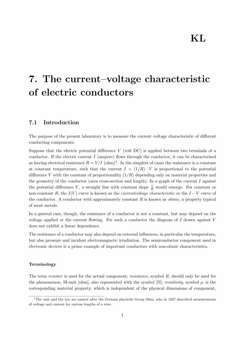
When the current–voltage characteristic is not linear, as in Fig. 7.1, we define the differential
resistance, also known as incremental resistance or slope resistance, as the inverse of the slope of
the characteristic at some particular value of voltage V0 (or current I0):
r(V0) =dV
dI
∣∣∣∣V0
≈ ∆V
∆I
∣∣∣∣V0
(7.4)
The differential resistance is important for the characterisation of many electronic components. In
the figure the resistance of the component is increasing with increasing voltage V .
Ohm’s law applies for conductors with constant R, thus the term ohmic conductor :
V = R · I (7.5)
In this case the current–voltage characteristic becomes a straight line with slope 1R ≡ 1
r , independent
of the voltage.
Laboratory Manuals for Physics Majors - Course PHY112/122
7.2. THEORY 3
ΔIΔV
I
VV0
I0
Figure 7.1: Illustration of differential changes of current and voltage at some arbitrary point V0 of
the current–voltage characteristic.
b) Metallic conductors
The conductivity of metals is determined mainly by the concentration of free electrons2. Free
electrons are non-local electrons that are not involved in chemical bonds and therefore easily move
through the lattice of a solid. Free electrons, despite the name, are still subject to interactions,
most importantly inelastic scattering at local electrical potentials, and are influenced by local
magnetic fields. Microscopically, electric conduction is a complicated process requiring a rigorous
quantum mechanical treatment, but for technical purposes may be described using the resistivity
ρ. For increasing temperature the mobility of the free electrons in metals decreases, such that the
resistance becomes an almost linear function of temperature, at least for temperature ranges not
too far from room temperature. We may describe this behaviour with a simple formula: Assume
that the metal has resistance R0 at temperature T0, usually 20C. Then we may write:
R = R0 · (1 + α(T − T0)) (7.6)
Note that this formula is approximative and purely phenomenological - it does not describe any
physical relationship, further, that it does not apply for very low and very high temperatures. The
temperature coefficient α, SI-unit [K−1] for pure metals typically have values in a narrow range
0.003 - 0.005. It is common practice to express the temperature coefficient as a percentage number,
which allows us to memorise the approximate expression 1/273 = 0.37 % per Kelvin. For some
alloys designed to be used for resistive heating, and therefore have a high resistivity and a low
temperature coefficient, such as manganin and constantan, the value of α is 0.008 and 0.002 % per
Kelvin respectively.
A formula useful for calculating the change in resistivity with change in temperature is easily
deduced from Eq. 7.6:
δρ = α · ∆T · ρ0 (7.7)
Here ρ0 is the resistivity at some reference temperature, usually 20C
2To some extent also bound electrons may contribute to conduction, as accommodated in the tight binding model
of electronic band structure.
Laboratory Manuals for Physics Majors - Course PHY112/122

4 7. The current–voltage characteristic of electric conductors
An electric current heats a metallic conductorThis is known as Joule heating, also known as ohmic
heating or resistive heating. So named after James Prescott Joule in 1841. produces a heating
power of P = V · I. If the heat is not removed through proper cooling, the temperature of
the conductor increases, which in turn increases the resistance according to Eq. 7.6. A metallic
conductor is thus an ohmic conductor only if the temperature remains constant through the design
of proper cooling.
c) Semiconductors
Semiconductors, such as gallium, germanium, silicon and gallium arsenide, typically have values of
resistivity in between those of insulators and metals. The temperature dependence is complicated,
and not well described by Eq. 7.6. If this formula is applied, it is valid only in a small temperature
range, and with negative values of the temperature coefficient3 α. For the case of a semiconductor
diode the temperature dependence is briefly touched upon in subsection d) of the theory section.
The advanced manufacturing technology developed for semiconductor electronic components per-
mits controlled production of semiconductor elements consisting of thin layers of different materials,
allowing the design of components with carrier concentrations and mobility varying in wide ranges
independent of external conditions. Examples demonstrated in this laboratory are thermistors and
light sensitive resistors.
Thermistors are widely used as inrush current limiters, temperature sensors, self-resetting over-
current protectors, and self-regulating heating elements. Thermistors are commonly made using a
ceramic or a polymer, and typically achieve high precision only within a limited temperature range,
usually 90 C to 130 C.
Assuming, as a first-order approximation, that for a thermistor the relationship between resistance
and temperature is linear, then:
∆R = k · ∆T (7.8)
where ∆R is the change in resistance, ∆T the corresponding change in temperature and k the
first-order temperature coefficient of resistance.
Thermistors are characterised by strong temperature dependence, and are classified into two main
types, depending on the sign of the coefficient k. If k is positive, the resistance increases with
increasing temperature, and the device is called a positive temperature coefficient (PTC) thermistor,
or posistor. Accordingly, if k is negative, the resistance decreases with increasing temperature, and
the device is called a negative temperature coefficient (NTC)-thermistor.
NTC-resistors are made from oxides of Cr, Mn and Fe and doped with small amounts of ions with
different valence. An example is Fe2O3, in which a small fraction of the Fe3+-Ions is replaced with
Fe2+ or Ti4+.
If a Fe3+ ion is replaced by a Fe2+, then the lower valency of the new ion requires one electron less to
be chemically bound in the crystal matrix. The excess electron is therefore only loosely bound, and
may become a free electron through thermal activation. With increasing temperature an increasing
3This is also the case for carbon, which was used for the filament by Edison in his first light bulbs.
Laboratory Manuals for Physics Majors - Course PHY112/122
7.2. THEORY 5
number of electrons becomes available for electric conduction through thermal activation. Corre-
sponding to the larger number of conduction electrons, the resistance of the material is reduced.
Typical temperature coefficients for NTCs lies between -2% and -6% per Kelvin. NTC-thermistors
may be utilised for temperature measurement devices, or as sensors in temperature controllers.
In a somewhat more involved manner, PTC-thermistors can be manufactured, e.g. using BaTiO3.
Temperature coefficients of PTCs may in certain temperature intervals become as large as 100%
per Kelvin. PTC-components are used e.g. for limiting excess voltage or current, for current
stabilisation and high voltage spark suppression.
Light sensitive resistors (LDR or ’light dependent resistors’) may be made of cadmium sulphide,
CdS, a compound well known for absorbing light that releases electrons and thereby changes the
conductivity. Sensors using CdS were previously common in exposure meters for photography, but
has been replaced by other designs because of the relatively low sensitivity of CdS.
d) Diodes – solid state and gaseous state
Diodes4 are electronic components with two external terminals. Diodes have an immensely impor-
tant role in electronics.
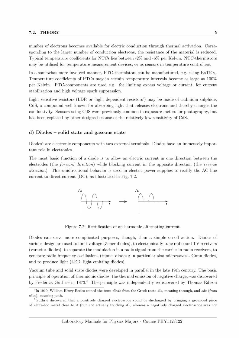
The most basic function of a diode is to allow an electric current in one direction between the
electrodes (the forward direction) while blocking current in the opposite direction (the reverse
direction). This unidirectional behavior is used in electric power supplies to rectify the AC line
current to direct current (DC), as illustrated in Fig. 7.2.
I
t
I
t
Figure 7.2: Rectification of an harmonic alternating current.
Diodes can serve more complicated purposes, though, than a simple on-off action. Diodes of
various design are used to limit voltage (Zener diodes), to electronically tune radio and TV receivers
(varactor diodes), to separate the modulation in a radio signal from the carrier in radio receivers, to
generate radio frequency oscillations (tunnel diodes); in particular also microwaves - Gunn diodes,
and to produce light (LED, light emitting diodes).
Vacuum tube and solid state diodes were developed in parallel in the late 19th century. The basic
principle of operation of thermionic diodes, the thermal emission of negative charge, was discovered
by Frederick Guthrie in 1873.5 The principle was independently rediscovered by Thomas Edison
4In 1919, William Henry Eccles coined the term diode from the Greek roots dia, meaning through, and ode (from
oδoς), meaning path.5Guthrie discovered that a positively charged electroscope could be discharged by bringing a grounded piece
of white-hot metal close to it (but not actually touching it), whereas a negatively charged electroscope was not
Laboratory Manuals for Physics Majors - Course PHY112/122

6 7. The current–voltage characteristic of electric conductors
on February 13, 18806.
Vacuum tube diodes: the thermionic valve diode
A vacuum tube diode is schematically shown to the left in Fig. 7.3.
I
V
V =anode
cathode
cathode heating voltage
Figure 7.3: Vacuum tube diode and typical current–voltage characteristic.
As indicated in the figure, the diode consists of two metallic electrodes enclosed in an evacuated
thin-walled glass tube. The lower electrode in the figure, the cathode, is provided with terminals
for a heating circuit, since the metal cathode has to be heated to glowing temperatures in order
for electrons to be easily emitted as a cloud of negative charge close to the cathode (thermionic
emission). If a potential difference of V (volt) is applied between the anode and the cathode, such
that the anode is positive relative to the cathode, the thermally emitted electrons at the cathode
will be attracted to the anode. A current then flows from the anode to the cathode (recall that the
direction of a current is by definition opposite to the transport of the negatively charged electrons).
If the potential difference of the anode is made lower than that of the cathode, electrons cannot be
extracted from the cloud at the cathode, and no current flows through the tube.
The current–voltage characteristic for a vacuum tube diode is shown to the right in Fig. 7.3. The
curve indicates that a small current flows even if no voltage is applied. This is because some
thermally activated electrons from the heated cathode have enough kinetic energy to reach the
anode. Only when a small negative potential difference is applied to the anode the current goes
to zero. Also note, that the characteristic attains saturation of the current: the plateau seen
for higher voltages. This occurs when the cloud of thermally activated electrons at the cathode
is depleted. If the rate of thermal excitation at the cathode is increased, e.g. through a higher
heating temperature, the plateau would be reached at a higher voltage V , with a higher current
flowing through the tube.
Vacuum tube diodes were dominating in electronic designs throughout the first half of the 20th
century. Since mid-century they were gradually replaced by semiconductor devices, which have the
benefit of being less bulky, and requiring no heating current. Vacuum tube technology remained
in use for applications requiring very high currents, as in high-power communication transmitters.
Today, at the beginning of the 21st century, vacuum tube components are obsolete, except in
discharged, indicating that electrical current flowed only in one direction.6Edison investigated carbon-filament light bulbs, and found that an invisible current could be drawn from the
glowing filament through the vacuum (or a low pressure noble gas filling) in the bulb, to a metal plate, but only when
the plate was connected to the positive terminal of the supply.
Laboratory Manuals for Physics Majors - Course PHY112/122
7.2. THEORY 7
specialised high-voltage equipment7.
Solid state diodes
In 1897 German physicist Karl Ferdinand Braun discovered the principle of current rectification in
certain crystals. The first semiconductor diodes, called cat’s whisker diodes, were made of crystals
of minerals such as galena, and equipped with thin contact wires.
Although the physics involved is quite different, the basic principles for vacuum tube diodes and
semiconductor diodes are equivalent: an excess charge of free carrier must be provided.
In a semiconductor this is achieved through an ingenious contraption: the p-n junction8. As the
name of the component implies, it is a combination of two parts.
Two of the most common semiconductor materials are silicon and gallium arsenide9. Both have four
valence electrons. The addition of dopant atoms with five valence electrons creates free electrons
since only four are required for binding the atom in the crystal matrix. Because of the excess
negative charge carriers the semiconductor is then said to be an n-type semiconductor.
Substituting dopant atoms with three valence electrons means that one electron per dopant atom
will be missing, which is equivalent to the presence of positive charges, ’holes’, in the crystal matrix.
A crystal that contains these formally positive charge carriers is called a p-type semiconductor.
In practice it is not possible to join two pieces of p- and n-type semiconductor crystals. A semi-
conductor diode is manufactured from a piece of single crystal semiconductor. Through a diffusion
process, a precisely controlled amount of impurities (dopants) are added in order to create a region
of p-type material in contact with a region of n-type material; this is a p-n junction.
The two types of carrier do not remain in their respective region of origin. Since they are free
carriers, albeit of different kind, they diffuse and recombine - they annihilate - thus forming a
region depleted of free charges10 across the p-n junction.
The depleted region contains fixed ions built into the lattice, which in the case of the n-type material
contribute a distributed positive charge, and the p-type negative charge. This means that the fixed
charges set up an internal electrical potential barrier over the p-n junction11. The field generated
by the space charge tends to counteract the diffusion of charge carriers into the depleted junction,
thus, at equilibrium, creating a concentration profile.
For many applications, it is common to speak of the voltage applied over the diode as bias voltage,
or simply bias, which is an important notion since the diode may be polarised either way. With the
7Vacuum tubes may occasionally also be found in esoteric niche applications, such as in electric guitar amplifiers
and so called high-end audio amplifiers, where they allegedly contribute to desirable qualities of sound, albeit for
very contrary reasons.8The p-n junction provides the basic function in almost all semiconductor electronic devices, such as diodes,
transistors, solar cells, LEDs, and integrated circuits. The discovery of the p–n junction is usually attributed to
American physicist Russell Ohl of Bell Laboratories.9Germanium is not anymore common in commercial components
10Also called a space charge region or depletion layer11There is an electric field directed from the n-type side to the p-type side
Laboratory Manuals for Physics Majors - Course PHY112/122

8 7. The current–voltage characteristic of electric conductors
p-type side of the diode on a positive potential (positive anode) and the n-type side to the negative,
we have what is called forward bias. The diode conducts current from the p-type side (the anode)
to the n-type side (the cathode) when the external potential overcomes the internal field, and the
current rapidly increases with the voltage applied.
In the forward direction of the diode, holes in the p-type region and the electrons in the n-type
region are pushed towards the depleted junction by the external field. This reduces the width of the
depletion zone, and lowers the potential barrier. For a certain forward bias voltage charge carriers
start moving across the p-n junction: the diode becomes conducting.
The current consists of electrons travelling from the n-type region toward the junction, and holes
flowing from the p-type region in the opposite direction toward the junction. The two kinds of
carriers constantly recombine in the vicinity of the junction. The electrons and holes travel in
opposite directions, but have opposite charges, so both contribute to the resulting electric current.
Reversing the polarity, making the p-type side (anode) negative negative, the voltage at the cathode
becomes higher than at the anode; the diode is working in the reverse bias region. The positive
carriers (holes) in the p-type material are pulled away from the junction, causing the width of the
depletion zone to increase. Similarly, because the n-type region is now positive, also the electrons
will be pulled away from the junction. Thus the voltage barrier over the junction increases, causing
an increased resistance to the flow of both kinds of charge carriers, only allowing a small leakage
of electric current across the p-n junction.
For large reverse bias, beyond what is the highest reverse operating voltage for normal diode
performance, the peak inverse voltage (PIV), the potential difference causes what is known as a
breakdown of the diode, creating large amount of additional pairs of oppositely charged carriers,
and drawing them through the barrier until the diode is permanently destroyed because of the
high current. Accordingly this region is known as the breakdown region of the current-voltage
characteristic. The breakdown voltage, depending on the type of diode, may be in the range 10 V
to 10 kV.
Without going into details, semiconductor diodes have a complex non-linear electrical behaviour,
which can be tailored through the doping process. A typical current–voltage characteristic for a
simple semiconductor diode is shown in Fig. 7.4.
I
V
reverse bias forward bias
Figure 7.4: Typical current–voltage characteristic for a simple semiconductor diode.
Several different types of diodes have been designed to use this to advantage. The avalanche diode
Laboratory Manuals for Physics Majors - Course PHY112/122

7.2. THEORY 9
is deliberately designed to be used in the avalanche region. For the zener diode, the concept of PIV
is not applicable. A zener diode contains a heavily doped p-n junction, allowing electrons to tunnel
through the potential barrer from the p-type material to the n-type material. The doping process
determines the maximum reverse voltage desired (called the zener voltage). Destructive avalanche
does not occur. Both devices, however, do have a limit to the maximum current and power in the
conducting reverse voltage region.
In the region of reverse bias smaller than the PIV, for a normal rectifier diode, the current through
the device is very low (in the µA range). This current is temperature dependent, however, and
at suffiently high temperatures, a substantial amount of reverse current can be observed (mA or
more). In the region of small forward bias, only a small forward current is conducted.
As the forward potential difference (the bias) is increased above an arbitrarily defined cut-in voltage,
also called on-voltage (onset of forward conduction) or more formally diode forward voltage drop,
(Vd), the diode current becomes appreciable, and the resistance over the diode low. In a normal
silicon diode, the forward bias voltage is typically 0.6 to 0.7 volts.
The current–voltage curve is exponential beyond the forward bias voltage Vd, which is a character-
istic of the diode type. Schottky diodes can be rated as low as 0.2 V, and red or blue light-emitting
diodes (LEDs) can have values of 1.4 V and 4.0 V respectively. At higher currents the forward
voltage drop over the diode increases. A drop of 1 V to 1.5 V is typical at full rated current for
power diodes.
The Shockley ideal diode equation12, also known as the diode law, represents the IV characteristic
of an ideal diode for either forward or reverse bias (in particular also for no bias voltage):
I = IS (eVD/(nVT ) − 1) (7.9)
where I is the diode current, IS is the reverse bias saturation current, VD the voltage across the
diode (the bias), and n the so called emission coefficient, also known as the ideality factor, which
is between about 1 to 2 depending on the fabrication process and semiconductor material. The
thermal voltage VT is a characteristic property of the junction defined as:
VT =k T
q(7.10)
with k Boltzmann’s constant, T the absolute temperature. and q the magnitude of the electrical
charge of the electron.
e) Electric glow discharge
An electric glow discharge may appear between two electrodes with a relative potential difference of
100 V to several kV. A typical device utilises electrodes inserted in a gas cell commonly filled with
argon at some low pressure of about 10–1000 Pa. There is no hot cathode: the process works at
ambient temperature. The ensuing current creates a plasma of ions and electrons. This principle is
12Named after transistor co-inventor William Bradford Shockley, not to be confused with tetrode inventor Walter
H. Schottky.
Laboratory Manuals for Physics Majors - Course PHY112/122

10 7. The current–voltage characteristic of electric conductors
put to work in products such as fluorescent lights and plasma-screen televisions. It finds scientific
applications in plasma physics and analytical chemistry. It was earlier used as power-on indicator
in consumer product (kitchen stoves) as well as industrial products, since the power consumption
may be very low, and the device has almost unlimited life.
The DC glow discharge is the most straightforward application. A small fraction of the population
of the gas atoms within the cell is initially in a ionized state through random processes, mostly
thermal collisions. The electric potential difference accelerates positively charged ions towards the
cathode and electrons towards the anode. Ions and electrons in turn collides with neutral atoms,
thus creating more ions and electrons. The potential difference applied between the electrodes
maintains a steady population of ions and electrons in the gas cell.
Some of the kinetic energy of the ions is transferred to the cathode, in part through ions striking
the cathode directly. The primary mechanism, is that ions strike the more numerous neutral gas
atoms, thus transferring a portion of their energy to them, which then strike the cathode. Whichever
species (ions or atoms) strike the cathode, the energy transferred redistribute and causes atoms
from the cathode to be ejected, typically in the form of free atoms. This process is known as
sputtering, which is also a general method implemented for depositing thin layers of material on a
target sample, for instance as insulating layers on a conductor.
The atoms released from the cathode have enough energy to drift into the bulk of the glow discharge,
where they may become excited through interaction with ions, electrons, or other atoms that have
been previously excited by collisions. Once excited, atoms will lose their energy fairly quickly. Of
the various ways that this energy can be lost, the most important is by emission of light. In optical
atomic spectroscopy, the wavelength of light can be used to identity the atom (i.e., the chemical
element). The intensity of light, i.e. the number of photons emitted, is directly proportional to
the concentration of that element in the sample. Glow discharge may therefore be implemented
in an apparatus with provision for changing the cathode material, which becomes a sample for
identification.
The principle may also be put to use in mass spectroscopy. Some collisions of energy high enough
will cause ionisation, creating ions that may be detected in atomic mass spectrometry, thus iden-
tifying the type of atom and the isotope, and the abundance of atoms and isotopes in the sample.
Laboratory Manuals for Physics Majors - Course PHY112/122
7.3. EXPERIMENTAL 11
7.3 Experimental
In the first part of this laboratory we measure the current–voltage characteristic of an ohmic resistor,
a light bulb and a diode. In addition, we qualitatively investigate the dependence on temperature
of a thermistor, and the influence of electromagnetic radiation on a light sensitive resistor.
The circuit is shown in Fig. 7.5. The component investigated (resistor, light bulb etc.) is connected
to a DC source. The current I and the voltage V is measured with two digital multimeters.
Caution: Take care not to increase currents and voltages beyond the respective maximum values.
V RL R =L +_power supply
0 - 12 V
IRi
resistor orlight bulb ordiode
Figure 7.5: Electrical circuit for measurement of current–voltage characteristic of an ohmic resistor,
light bulb and diode.
The input resistance Ri of the voltmeter has to be accounted for when the current is determined.
The input resistance may be regarded as a serial ohmic resistor through which part of the current
is passing. This means that the indicated current I is not the actual current in the circuit.
• Connect the components of the circuit as shown in Fig. 7.5.
• Determine the input resistance of the voltmeter without connecting RL.
• Connect the ohmic resistor RL to the circuit. Observe qualitatively the dependence of current
on voltage in order to determine voltage increments for the measurement of the current–
voltage characteristic. Where the current does not change much the voltage may be increased
in larger steps (of the order 1 V), whereas smaller steps (of the order 0.1 V) should be used
where the current increases strongly. Prepare a table for the data accordingly.
• Measure the current I as a function of the voltage V as prepared.
• Reverse the polarity of the voltage source and repeat the measurement.
• Correct for the influence of the input resistance of the voltmeter where this is appropriate.
Draw a graph of the current–voltage characteristic on millimeter ruled graph paper.
• Determine from the measured currentvoltage characteristic the differential resistance r =
dV/dI and draw a graph of r as function of voltage.
Laboratory Manuals for Physics Majors - Course PHY112/122
12 7. The current–voltage characteristic of electric conductors
• Repeat the measurements for the light bulb.
• Repeat the measurements for the diode.
Caution: The current may increase rapidly in a certain voltage range, both for forward and
reverse bias.
• Qualitatively investigate the dependence of the resistance of the thermistor on temperature.
• Qualitatively investigate the dependence of the light sensitive resistor on light intensity.
V glow dischargelamp
power supply 0 - 300 V
220 kΩI
3 mA
Ri
Figure 7.6: Circuit for measuring the the current–voltage characteristic for the glow discharge lamp.
In the second part of the laboratory the current–voltage characteristic for a glow discharge lamp
is measured. The circuit employed is shown Fig. 7.6. Note: The series resistance of 220 kΩ is
necessary in order to prevent excessive currents.
• Measure the current as function of voltage. Increase the voltage in steps of 20 V until the
lamp turns on, and then in steps of about 5 V. Subsequently reduce the voltage in steps of
10 V until the lamp turns off.
• If necessary correct the currents measured for the input resistance of the voltmeter. Draw
the measured current–voltage characteristic on graph paper.
• Determine from the measured current–voltage characteristic the differential resistance r =
dV/dI and draw a graph of r as function of voltage.
Laboratory Manuals for Physics Majors - Course PHY112/122