letter open access fabrication of a 3 dimensional
TRANSCRIPT

Lee et al. Micro and Nano Systems Letters 2013, 1:5http://www.mnsl-journal.com/content/1/1/5
LETTER Open Access
Fabrication of a 3 dimensional dielectrophoresiselectrode by a metal inkjet printing methodSeung Hyun Lee1, Gyu-Young Yun2, Yul Koh1, Sang-Ho Lee2* and Yong-Kweon Kim1*
Abstract
We proposed a micro electrode fabrication method by a metal inkjet printing technology for the bio-applications ofdielectrophoresis (DEP). The electrodes are composed of bottom planar gold (Au) electrodes and three dimensional(3D) silver (Ag) electrodes fabricated locally on the Au electrode through metal inkjet printing. We observed thenegative DEP characteristics of the 4 μm polystyrene beads on the both electrodes at the 500 kHz, AC 20 Vpp point.The number of beads trapped on the printed Ag electrode is 79 and 25 on the planar Au electrode because ofspatially larger electric field in a 3D electrode system.
Keywords: Metal inkjet printing technology; Dielectrophoresis (DEP); 3D electrode
IntroductionThree dimensional (3D) electrodes are effectively used ina wide range of applications such as electronic circuitcomponents, micro sensors, micro actuators, and micro-fluidic system. In particular, the 3D electrode is usefulfor the dielectrophoresis (DEP) of biological samplesincluding cells, proteins, and particles. Compared to theplanar electrode, the 3D electrode structure allows it totransmit a large DEP force to the biological samples dueto the high gradient electrical field generated betweenthe 3D electrodes [1]. Therefore, the high gradient elec-trical field in 3D DEP chips could enhance separationand trapping performance. There are many investiga-tions into the trapping and separation of a biologicalsample using 3D DEP chips.Conventional microfabrication technologies have sev-
eral drawbacks in 3D electrode fabrication. It is difficultto form 3D electrodes that have a micrometer scalethickness using thermal evaporation and sputtering.Metal electroplating can be used to fabricate 3D elec-trodes with high aspect ratios, but complicated proce-dures are required. The inkjet printing technology hasbeen studied for the patterning of the 3D electrode.Inkjet printing can be directly utilized in fabricating 3D
* Correspondence: [email protected]; [email protected] Institute of Industrial Technology, Ansan, Korea1School of Electrical Engineering and Computer Science, Seoul NationalUniversity, Seoul, KoreaFull list of author information is available at the end of the article
© 2013 Lee et al.; licensee Springer. This is an OAttribution License (http://creativecommons.orin any medium, provided the original work is p
structures with a simple process at short run-time andlow cost. The inkjet printing method does not requirecomplicated additional fabrication process steps such asphotoresist mold and metal seed layer formation forelectroplating, in order to pattern a 3D metal structure. Forexample, various metals can be directly patterned using ink-jet printing on the substrate by consuming a small metalsource. Therefore, inkjet printing is a very suitable technol-ogy to fabricate a 3D metal structure. However, the inkjetprinting technology has not yet been applied to the micro-fluidic systems due to its low fabrication resolution [2-4].We propose a metal inkjet printing method for the
fabrication of the 3D DEP electrode for micro particlesmanipulation in a microfluidic chamber. For a high reso-lution inkjet printing, fluorocarbon (FC) film patterningwas utilized to make the ink-phobic boundaries whichprevent droplets from spreading and enable selectivepatterning. A microfluidic chamber was assembled with theelectrode chip after printing silver (Ag) 3D electrodes forprotecting particles and adjusting for fluid control. TheDEP performance was verified using the 4 μm polystyrenebeads and AC drive voltage control [5-7].
FindingsFabrication processThe FC film as an ink-spreading barrier was selectivelypatterned on the gold (Au) film to print thick 3D DEPelectrodes in a precisely defined printing area. The fabri-cation processes are presented in Figure 1. First, the Au
pen Access article distributed under the terms of the Creative Commonsg/licenses/by/2.0), which permits unrestricted use, distribution, and reproductionroperly cited.

Figure 1 The process of DEP chip fabrication. (a) Au planar electrode fabrication with lift-off process and Cr/Au thermal evaporation. (b) AZ 4330PR patterning on the Au electrode surface where the Ag will be printed. (c) Fluorocarbon (FC) coating on the surface and sintering. (d) Removing AZ4330 PR on the Au electrode. (e) Printing Ag inkjet on the Au electrode surface where FC is not coated. (f) Bonding with PDMS chamber.
(a)
(b)
Figure 2 The process of Ag inkjet printing. (a) Several Agdroplets were jetted inside a rectangular printing region, (b) Thesesmall droplets agglomerate together to form larger clusters.
Lee et al. Micro and Nano Systems Letters 2013, 1:5 Page 2 of 7http://www.mnsl-journal.com/content/1/1/5
planar electrode (0.3 μm thickness) was fabricated onthe substrate by a conventional lift-off process by photolith-ography and Cr/Au thermal evaporation (Figure 1(a)). Topattern the surface with hydrophilic and hydrophobicregions selectively, the photoresist (AZ4330) mold wasfirst patterned on the Au bottom electrodes. Then, thefluorocarbon (FC) solution was coated on the surfaceand photoresist mold (Figure 1(b) and (c)). We used aFC-722 solution diluted with FC-40 (3 M fluorinert™)at a ratio of 4:1 for surface coating to make the surfacehydrophobic. The FC film on the photoresist mold wasremoved by a lift-off process after curing at 100°C for15 min (Figure 1(d)). Silver was inkjet printed to formthick 3D electrodes inside the printing area as definedby the patterned hydrophobic FC film. Furthermore,the printed Ag patterns were sintered at 200°C for 30 minto increase the conductivity and strength of adhesion be-tween the ink and substrate (Figure 1(e)). The used printingsystem is DMP-2800 from Fujifilm Dimatix Corporationand the Ag material is 40LT-15C silver jet ink produced byAdvanced Nano Product Corporation. Finally, the PDMSchamber was fabricated by a PDMS molding technology.The chamber and the glass substrate were bonded to eachother for the DEP experiments (Figure 1(f)).Figure 2 shows the printing process to fabricate elec-
trodes on the substrate. In the inkjet printing process(Figure 1(e)), fourteen Ag droplets (about 58.5 pl) wereprinted inside a rectangular printing region of 101.6 μm×3.9 mm in single printing. The inkjet printing fabricationresults are affected by the jetting position and the numberof metal inkjet droplets, so it is important to set the dropletjetting condition before the printing process. We sim-ply control the height of an electrode by regulating theoverlap-rate of the inkjet jetting.

Lee et al. Micro and Nano Systems Letters 2013, 1:5 Page 3 of 7http://www.mnsl-journal.com/content/1/1/5
Inkjet-printed 3D DEP chip designFigure 3 shows a schematic of the fabricated 3D DEP chip.The Au planar electrodes are fabricated on the glass wafer.The Au electrodes are patterned into the shape of a combdrive and used as bottom electrodes. An AC voltage signalis applied to the DEP chip trough the Au electrode. Thesize of the contact pad connected with the function gener-ator is 2 mm× 2 mm. The gold (Au) rectangular electrodesof 101.6 μm×3.9 mm were interdigitated with a gap of50.8 μm. Ag 3D electrodes of 10 μm thicknesses are formedon the rectangular Au electrode on the desired region asshown in Figure 3(b), and the size of the Ag 3D electrode is
(a)
(b)
Figure 3 Schematics of the DEP chip with the 3D printed electrodes.substrate and glass bottom substrate. The substrates are fabricated separatthe Au planar electrodes are patterned as a bottom electrode and Ag 3D eDEP chip and electrode: The scale of the DEP chip and Au, Ag electrodes.
101.6 μm×393.7 μm. The whole dimension of the DEPchip is 3 cm× 1 cm, and the electrodes don’t have integermultiple dimensions in meters. This is because the nozzlesize is fixed and the jetting inkjet is also restricted to inches.The polydimethylsiloxane (PDMS) chamber is used as acover to minimize the effects of external contamination asit bonds to the DEP chip. The PDMS chamber has inletand outlet holes to enable sample injection.
DEP characteristics of the beadsAccording to the direction of the DEP force, there aretwo types for the DEP characteristics: positive and
(a) Schematic of the DEP chip; the device consists of the PDMS topely from each other before being assembled. On the glass substrate,lectrodes are patterned locally on top of them. (b) The scale of the

Lee et al. Micro and Nano Systems Letters 2013, 1:5 Page 4 of 7http://www.mnsl-journal.com/content/1/1/5
negative DEP. The DEP force is expressed by equation(1) and (2).
FDEP ¼ 2πr3 ∈mRe f cm ωð Þ½ �∇ Ej j2 ω : angular velocity of the electric field ð1Þ
f CM ωð Þ ¼ ε0p ωð Þ−ε0m ωð Þ
ε0p ωð Þ þ 2ε0m ωð Þ
!εp : complex permittivity of the particleεp : complex permittivity of the medium
ð2Þ
The DEP force is positive when the Clausius-Mossotti(CM) factor (ƒCM) has a positive value while the negativeDEP force is generated when ƒCM has a negative value.Moreover, the electric field gradient and the radius of theparticles are directly affected by the DEP force [8]. Accord-ing to the electric field distribution, we can predict wherethe beads are trapped on the chip. In the positive DEP, theparticles are gathered toward the higher electric field regionwhile the particles move toward the lower electric field
(a)
(b)
Figure 4 The FEM simulations. (a) The electric field distribution on the eLine 1 is on the 3D electrodes and line 2 is on the planar electrodes. The x100 μm on 3D electrodes and 300 μm on planar electrodes.
region in the negative DEP. In the case of the polystyrenebead, it has negative DEP characteristics at almost everyfrequency range.Figure 4 shows the Finite Element Method (FEM) sim-
ulations of the electric field distribution and intensity forthe planar electrodes and the 3D electrodes. The electricfield distribution is presented in Figure 4(a). The electricfield generated between the 3D electrodes has a higherintensity than that between the planar electrodes. As
lectrode plane. (b) The electric field intensity on the electrode plane.axis of the simulation range is 0 μm to 1000 μm and the y axis are
Lee et al. Micro and Nano Systems Letters 2013, 1:5 Page 5 of 7http://www.mnsl-journal.com/content/1/1/5
shown in Figure 4(b), the electric field gradient for the3D electrode is 2 times larger than that for the planarelectrode, because the effective electric field range aroundthe 3D electrode is increased. Therefore, the beads canbe affected immensely by the electric field around the3D electrode and the trapping rate of the beads is alsohigher around the 3D electrode than around the planarelectrode [9-11].
Results and discussionInkjet printing is inherently problematic in that it is asolution based fabrication process; the ejected ink drop-let shows a different spreading behavior under differentsurface wettability after deposition onto substrates.Different spreads of the ink droplet make it difficult toapply the dimensional control of micron scale patternsof the inkjet printing to MEMS process. We solve thisissue by separating non-printing areas and printingareas through patterning FC film on ink-wettable sub-strates, because the FC film is well known to have lowsurface energy and poor wettability with various solutions.We can trap jetted Ag ink droplets only inside the ink-
(a)
(b)
Figure 5 Droplet generation and contact angle measurementaccording to FC solution treatment on the surface of thesubstrate. (a) The jetted droplet on the non-FC coated Au surface(b) The jetted droplet on the FC coated surface.
wettable printing areas surrounded by a FC film-based ink-spreading barrier. To investigate the wettability of Ag inkon the surface, we measured the contact angles of the Aginks onto each FC film and Au surface, because the print-ing area in the proposed fabrication process is affected bythe FC film patterning process. As shown in Figure 5, themeasured contact angle of the Ag ink surface is quite low,less than 10° on the Au surface. On the other hand, the Ag
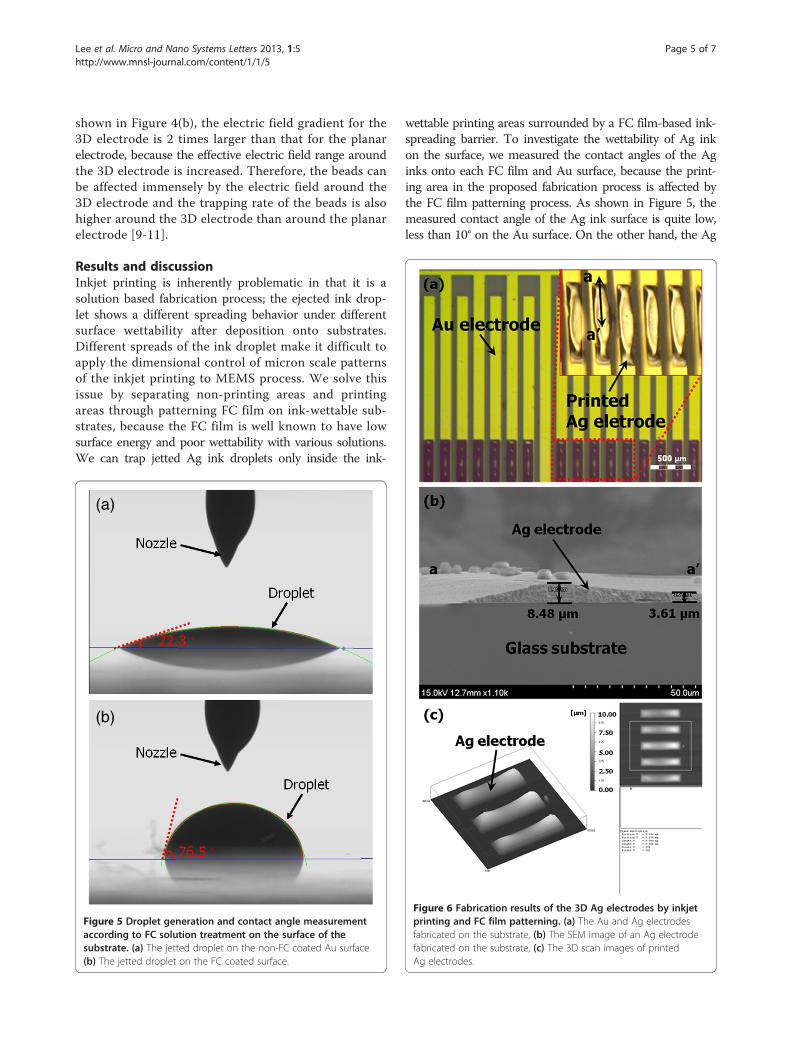
Figure 6 Fabrication results of the 3D Ag electrodes by inkjetprinting and FC film patterning. (a) The Au and Ag electrodesfabricated on the substrate, (b) The SEM image of an Ag electrodefabricated on the substrate, (c) The 3D scan images of printedAg electrodes.

Lee et al. Micro and Nano Systems Letters 2013, 1:5 Page 6 of 7http://www.mnsl-journal.com/content/1/1/5
ink droplet on the FC film surface doesn’t spread well andthe contact angle is 85.4°, which is much higher than thaton the Au surface. These results verified the fact that thehydrophobic FC film can be used as a barrier to control thespreading behavior of the Ag ink on the Au surface.The inset of Figure 6(a) shows Ag electrodes printed on
the Au electrodes inside a rectangular printing area sur-rounded by FC film. Ag ink spread and is trapped success-fully only on the Au surface without FC film, and FC filmacts as a barrier to prevent the ink from over-spreadingafter the ink-jetting process. However, the thickness of theAg electrode is not uniform and the edge shape is tilted, asshown in Figure 6(b). The overall morphology is similar toa dented rectangular with round corners (Figure 6(c)).This morphological characteristic would result from theso-called “coffee ring effect” where a ring-like pattern isformed by the accumulation of particles at the edgesthrough capillary flow induced by the differential evapor-ation rates across the drop. Ag particles inside the printedink droplet move toward the edges from the center and theparticle accumulation at the edge boundaries could resultin a dented rectangle with round corners [1]. For furtherresearch, the fabrication process needs to be improved toprovide rectangular shape of the printed structure by con-trolling the printing conditions like substrate temperature,surface wettability, and ink vapor pressure [12,13].Figure 7 shows the DEP characteristic of the 4 μm
polystyrene beads. The operational voltage was AC 20 Vpp
Figure 7 The results of the DEP experiment. (a) Initial state, (b) Applyin2D electrode, (d) on the 3D printed electrode.
and the applied frequency was 500 kHz. Under these condi-tions, micro beads represent a negative DEP characteristicon the Au and Ag electrodes, because these locations onthe electrodes have lower electric field intensity than otherlocations as shown in the simulation results of Figure 4. Inparticular, more beads gather on the Ag 3D electrodes sincethe 3D structure has a broad range of the DEP force asshown in Figure 7(c) and (d). The number of beads trappedon the Ag electrode is 79 and 25 on the Au electrode at theregions (dotted line) indicated by the arrow. The collectedbeads per unit area are approximately 3 times larger on theAg electrode than on the Au electrode. The reason for thisis that the electric field distribution is extensive around the3D electrode, and thus a large amount of the beads can bespatially exposed to the electric field. In the case of the pla-nar electrodes, an electric field distribution is concentratedon the surface of the micro DEP chip, especially at theedges among electrodes, so the electric field influence ismuch weaker in other areas. Thus, we confirmed that theexperimental results have similar trends compared to aprior prediction in the FEM simulation.
ConclusionIn this work, we successfully demonstrated the newfabrication method for fabricating 3D electrodes by ametal inkjet printing and selective FC film patterning.FC film patterning was very effective at making ink-phobic boundaries to prevent droplets from spreading
g AC 20 Vpp, 500 kHz, DEP characteristic of the microbeads (c) on the

Lee et al. Micro and Nano Systems Letters 2013, 1:5 Page 7 of 7http://www.mnsl-journal.com/content/1/1/5
after the Ag inkjet printing. Ag ink successfully spreadand was trapped only on the Au surface without FCfilm, while the FC films acted as a barrier to preventthe over-spreading after the ink-jetting process. Theoverall morphology resulted in a dented rectangle withrounded corners due to the coffee ring effect and thethickness of the Ag electrode is non-uniform. However,we could control the thickness of an electrode by regu-lating the overlap-rate of the inkjet jetting and thenumber of metal inkjet droplets. The DEP performanceof the inkjet-printed Ag electrodes was examined usingthe 4 μm polystyrene beads and AC drive voltage con-trol. We could confirm that more beads were trapped onthe 3D electrodes than on the planar electrodes becausea large amount of the beads could be spatially exposedto the high electric field in a 3D electrode system. Forfuture research, we need to improve the morphology ofthe printed structure by controlling printing conditionssuch as substrate temperature, surface wettability, andink vapor pressure.
Competing interestsThe authors declare that they have no competing interests.
Authors’ contributionsSHL carried out the experiments, analyzed the experimental results anddrafted the manuscript. G-YY performed the metal inkjet printing fabrication.YK, S-HL and Y-KK carried out experimental measurements. All authors readand approved the final manuscript.
AcknowledgementsThis work was supported by the Korea Institute of Industrial Technology.
Received: 23 September 2013 Accepted: 5 December 2013Published: 18 December 2013
References1. Pethig R (2010) Review article-dielectrophoresis: status of the theory,
technology, and applications. Biomicrofluidics 4, doi:10.1063/1.34566262. Shin KY, Lee SH, Oh JH (2011) Solvent and substrate effects on inkjet-printed
dots and lines of silver nanoparticle colloids. J Micromech Microeng 21,doi:10.1088/0960-1317/21/4/045012
3. Burns SE, Cain P, Mills J, Wang JZ, Sirringhaus H (2003) Inkjet printing ofpolymer thin-film transistor circuits. MRS Bull 28:829–834
4. de Gans BJ, Duineveld PC, Schubert US (2004) Inkjet printing of polymers:state of the art and future developments. Adv Mater 16:203–213
5. Bietsch A, Zhang JY, Hegner M, Lang HP, Gerber C (2004) Rapidfunctionalization of cantilever array sensors by inkjet printing.Nanotechnology 15:873–880
6. Lee HH, Chou KS, Huang KC (2005) Inkjet printing of nanosized silvercolloids. Nanotechnology 16:2436–2441
7. Son Y, Yeo J, Moon H, Lim TW, Hong S, Nam KH, Yoo S, Grigoropoulos CP,Yang DY, Ko SH (2011) Nanoscale electronics: digital fabrication by directfemtosecond laser processing of metal nanoparticles. Adv Mater 23:3176
8. Kim MS, Kim JH, Lee YS, Lim GG, Lee HB, Park JH, Kim YK (2009)Experimental and theoretical analysis of DEP-based particle deflection forthe separation of protein-bound particles. J Micromech Microeng 19,doi:10.1088/0960-1317/19/1/015029
9. Iliescu C, Tresset G, Xu GL (2009) Dielectrophoretic field-flow method forseparating particle populations in a chip with asymmetric electrodes.Biomicrofluidics 3, doi:10.1063/1.3251125
10. He HQ, Chang DC, Lee YK (2007) Using a micro electroporation chip todetermine the optimal physical parameters in the uptake of biomoleculesin HeLa cells. Bioelectrochemistry 70:363–368
11. Cheng IF, Froude VE, Zhu YX, Chang HC, Chang HC (2009) A continuoushigh-throughput bioparticle sorter based on 3D traveling-wavedielectrophoresis. Lab Chip 9:3193–3201
12. Soltman D, Subramanian V (2008) Inkjet-printed line morphologies andtemperature control of the coffee ring effect. Langmuir 24:2224–2231
13. de Gans BJ, Schubert US (2004) Inkjet printing of well-defined polymer dotsand arrays. Langmuir 20:7789–7793
doi:10.1186/2213-9621-1-5Cite this article as: Lee et al.: Fabrication of a 3 dimensionaldielectrophoresis electrode by a metal inkjet printing method. Micro andNano Systems Letters 2013 1:5.
Submit your manuscript to a journal and benefi t from:
7 Convenient online submission
7 Rigorous peer review
7 Immediate publication on acceptance
7 Open access: articles freely available online
7 High visibility within the fi eld
7 Retaining the copyright to your article
Submit your next manuscript at 7 springeropen.com