lm2738 550-khz/1.6-mhz 1.5-a step-down dc-dc … · lm2738 v in v in boost en sw fb gnd v out c3 c1...
TRANSCRIPT
LM2738
VIN VIN
EN
BOOST
SW
FBGND
VOUT
C3 L1C1
C2
R1
R2
D1
D2
ON
OFF
Product
Folder
Sample &Buy
Technical
Documents
Tools &
Software
Support &Community
An IMPORTANT NOTICE at the end of this data sheet addresses availability, warranty, changes, use in safety-critical applications,intellectual property matters and other important disclaimers. PRODUCTION DATA.
LM2738SNVS556C –APRIL 2008–REVISED JANUARY 2016
LM2738 550-kHz/1.6-MHz 1.5-A Step-Down DC-DC Switching Regulator
1
1 Features1• Space-Saving WSON and MSOP-PowerPAD™
Packages• 3-V to 20-V Input Voltage Range• 0.8-V to 18-V Output Voltage Range• 1.5-A Output Current• 550-kHz (LM2738Y) and 1.6-MHz (LM2738X)
Switching Frequencies• 250-mΩ NMOS Switch• 400-nA Shutdown Current• 0.8-V, 2% Internal Voltage Reference• Internal Soft-Start• Current-Mode, PWM Operation• Thermal Shutdown
2 Applications• Local Point of Load Regulation• Core Power in HDDs• Set-Top Boxes• Battery Powered Devices• USB Powered Devices• DSL Modems
3 DescriptionThe LM2738 regulator is a monolithic, high-frequency, PWM step-down DC-DC converter in an 8-pin WSON or 8-pin MSOP-PowerPAD package. Itprovides all the active functions for local DC-DCconversion with fast transient response and accurateregulation in the smallest possible PCB area.
With a minimum of external components, the LM2738is easy to use. The ability to drive 1.5-A loads with aninternal 250-mΩ NMOS switch using state-of-the-art0.5-µm BiCMOS technology results in the best powerdensity available. Switching frequency is internally setto 550 kHz (LM2738Y) or 1.6 MHz (LM2738X),allowing the use of extremely small surface-mountinductors and chip capacitors. Even though theoperating frequencies are very high, efficiencies up to90% are easy to achieve. External enable is included,featuring an ultralow standby current of 400 nA. TheLM2738 utilizes current-mode control and internalcompensation to provide high-performance regulationover a wide range of operating conditions. Additionalfeatures include internal soft-start circuitry to reducein-rush current, cycle-by-cycle current limit, thermalshutdown, and output over-voltage protection.
Device Information(1)
PARTNUMBER PACKAGE BODY SIZE (NOM)
LM2738WSON (8) 3.00 mm × 3.00 mmMSOP-PowerPAD (8) 3.00 mm × 3.00 mm
(1) For all available packages, see the orderable addendum atthe end of the data sheet.
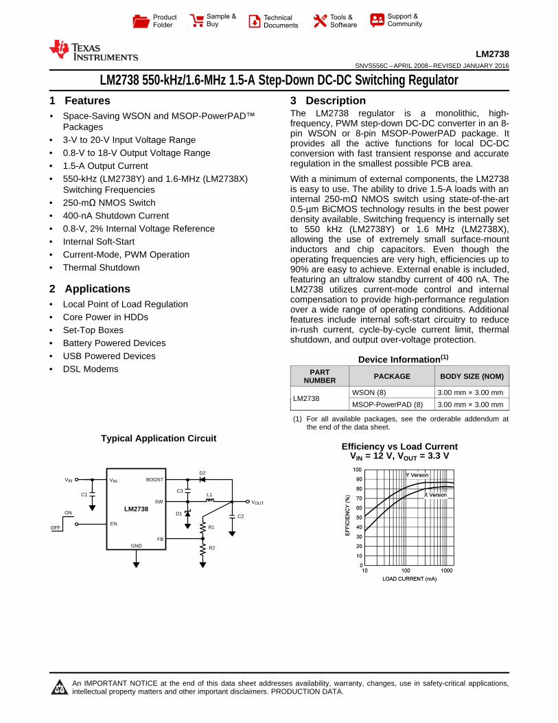
Typical Application CircuitEfficiency vs Load Current
VIN = 12 V, VOUT = 3.3 V

2
LM2738SNVS556C –APRIL 2008–REVISED JANUARY 2016 www.ti.com
Product Folder Links: LM2738
Submit Documentation Feedback Copyright © 2008–2016, Texas Instruments Incorporated
Table of Contents1 Features .................................................................. 12 Applications ........................................................... 13 Description ............................................................. 14 Revision History..................................................... 25 Pin Configuration and Functions ......................... 36 Specifications......................................................... 4
6.1 Absolute Maximum Ratings ...................................... 46.2 ESD Ratings.............................................................. 46.3 Recommended Operating Conditions....................... 46.4 Thermal Information .................................................. 56.5 Electrical Characteristics........................................... 56.6 Typical Characteristics .............................................. 6
7 Detailed Description ............................................ 107.1 Overview ................................................................. 107.2 Functional Block Diagram ....................................... 117.3 Feature Description................................................. 117.4 Device Functional Modes........................................ 14
8 Application and Implementation ........................ 158.1 Application Information............................................ 158.2 Typical Applications ................................................ 15
9 Power Supply Recommendations ...................... 3010 Layout................................................................... 30
10.1 Layout Guidelines ................................................. 3010.2 Layout Example .................................................... 3110.3 Thermal Considerations ........................................ 31
11 Device and Documentation Support ................. 3311.1 Device Support...................................................... 3311.2 Documentation Support ........................................ 3311.3 Community Resources.......................................... 3311.4 Trademarks ........................................................... 3311.5 Electrostatic Discharge Caution............................ 3311.6 Glossary ................................................................ 33
12 Mechanical, Packaging, and OrderableInformation ........................................................... 33
4 Revision HistoryNOTE: Page numbers for previous revisions may differ from page numbers in the current version.
Changes from Revision B (April 2013) to Revision C Page
• Added Device Information table, ESD Ratings table, Thermal Information table, Feature Description section, DeviceFunctional Modes, Application and Implementation section, Power Supply Recommendations section, Layoutsection, Device and Documentation Support section, and Mechanical, Packaging, and Orderable Information section...... 1
Changes from Revision A (April 2013) to Revision B Page
• Changed layout of National Data Sheet to TI format ........................................................................................................... 29

3
LM2738www.ti.com SNVS556C –APRIL 2008–REVISED JANUARY 2016
Product Folder Links: LM2738
Submit Documentation FeedbackCopyright © 2008–2016, Texas Instruments Incorporated
(1) I = Input, O = Output, and PWR = Power
5 Pin Configuration and Functions
NGQ Package8-Pin WSON With Exposed Thermal Pad
Top View
DGN Package8-Pin MSOP-PowerPAD
Top View
Pin FunctionsPIN
TYPE (1) DESCRIPTIONNO. NAME
1 BOOST I Boost voltage that drives the internal NMOS control switch. A bootstrap capacitor isconnected between the BOOST and SW pins.
2 VIN PWR Supply voltage for output power stage. Connect a bypass capacitor to this pin. Must tie pins2 and 3 together at package.
3 VCC I Input supply voltage of the device. Connect a bypass capacitor to this pin. Must tie pins 2and 3 together at the package.
4 EN I Enable control input. Logic high enables operation. Do not allow this pin to float or be greaterthan VIN + 0.3 V.
5, 7 GND PWR Signal and power ground pins. Place the bottom resistor of the feedback network as close aspossible to these pins.
6 FB I Feedback pin. Connect FB to the external resistor divider to set output voltage.8 SW O Output switch. Connects to the inductor, catch diode, and bootstrap capacitor.DAP GND — Signal and power ground. Must be connected to GND on the PCB.

4
LM2738SNVS556C –APRIL 2008–REVISED JANUARY 2016 www.ti.com
Product Folder Links: LM2738
Submit Documentation Feedback Copyright © 2008–2016, Texas Instruments Incorporated
(1) Stresses beyond those listed under Absolute Maximum Ratings may cause permanent damage to the device. These are stress ratingsonly, which do not imply functional operation of the device at these or any other conditions beyond those indicated under RecommendedOperating Conditions. Exposure to absolute-maximum-rated conditions for extended periods may affect device reliability.
(2) If Military or Aerospace specified devices are required, contact the Texas Instruments Sales Office or Distributors for availability andspecifications.
6 Specifications
6.1 Absolute Maximum Ratingsover operating free-air temperature range (unless otherwise noted) (1) (2)
MIN MAX UNITVIN, VCC –0.5 24 VSW voltage –0.5 24 VBoost voltage –0.5 30 VBoost to SW voltage –0.5 6 VFB voltage –0.5 3 VEN voltage –0.5 VIN + 0.3 VJunction temperature 150 °C
Soldering informationInfrared and convection reflow (15 s) 220 °CWave soldering lead temperature (10 s) 260 °C
Storage temperature, Tstg –65 150 °C
(1) JEDEC document JEP155 states that 500-V HBM allows safe manufacturing with a standard ESD control process.(2) Human body model, 1.5 kΩ in series with 100 pF.
6.2 ESD RatingsVALUE UNIT
V(ESD) Electrostatic discharge Human-body model (HBM), per ANSI/ESDA/JEDEC JS-001 (1) (2) ±2000 V
6.3 Recommended Operating Conditionsover operating free-air temperature range (unless otherwise noted)
MIN MAX UNITVIN, VCC 3 20 VSW voltage –0.5 20 VBoost voltage –0.5 25.5 VBoost to SW voltage 2.5 5.5 VJunction temperature −40 125 °CThermal shutdown 165 °C
5
LM2738www.ti.com SNVS556C –APRIL 2008–REVISED JANUARY 2016
Product Folder Links: LM2738
Submit Documentation FeedbackCopyright © 2008–2016, Texas Instruments Incorporated
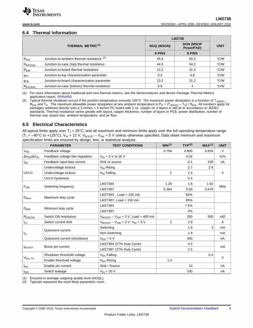
(1) For more information about traditional and new thermal metrics, see the Semiconductor and device Package Thermal Metricsapplication report, SPRA953.
(2) Typical thermal shutdown occurs if the junction temperature exceeds 165°C. The maximum power dissipation is a function of TJ(MAX) ,RθJA and TA . The maximum allowable power dissipation at any ambient temperature is PD = (TJ(MAX) – TA) / RθJA. All numbers apply forpackages soldered directly onto a 3 inches × 3 inches PC board with 2 oz. copper on 4 layers in still air in accordance to JEDECstandards. Thermal resistance varies greatly with layout, copper thickness, number of layers in PCB, power distribution, number ofthermal vias, board size, ambient temperature, and air flow.
6.4 Thermal Information
THERMAL METRIC (1)
LM2738
UNITNGQ (WSON) DGN (MSOPPowerPAD)
8 PINS 8 PINSRθJA Junction-to-ambient thermal resistance (2) 45.9 50.3 °C/WRθJC(top) Junction-to-case (top) thermal resistance 44.6 54.2 °C/WRθJB Junction-to-board thermal resistance 13.2 31.4 °C/WψJT Junction-to-top characterization parameter 0.5 4.8 °C/WψJB Junction-to-board characterization parameter 13.2 31.2 °C/WRθJC(bot) Junction-to-case (bottom) thermal resistance 5.8 4 °C/W
(1) Ensured to average outgoing quality level (AOQL).(2) Typicals represent the most likely parametric norm.
6.5 Electrical CharacteristicsAll typical limits apply over TJ = 25°C, and all maximum and minimum limits apply over the full operating temperature range(TJ = –40°C to +125°C). VIN = 12 V, VBOOST – VSW = 5 V unless otherwise specified. Data sheet minimum and maximumspecification limits are ensured by design, test, or statistical analysis.
PARAMETER TEST CONDITIONS MIN (1) TYP (2) MAX (1) UNITVFB Feedback voltage 0.784 0.800 0.816 VΔVFB/ΔVIN Feedback voltage line regulation VIN = 3 V to 20 V 0.02 %/VIFB Feedback input bias current Sink or source 0.1 100 nA
UVLOUndervoltage lockout VIN Rising 2.7 2.9
VUndervoltage lockout VIN Falling 2 2.3UVLO hysteresis 0.4
FSW Switching frequencyLM2738X 1.28 1.6 1.92
MHzLM2738Y 0.364 0.55 0.676
DMAX Maximum duty cycleLM2738X , Load = 150 mA 92%LM2738Y, Load = 150 mA 95%
DMIN Minimum duty cycleLM2738X 7.5%LM2738Y 2%
RDS(ON) Switch ON resistance VBOOST – VSW = 3 V, Load = 400 mA 250 500 mΩICL Switch current limit VBOOST – VSW = 3 V, VIN = 3 V 2 2.9 A
IQQuiescent current
Switching 1.9 3 mANon-Switching 1.9 mA
Quiescent current (shutdown) VEN = 0 V 400 nA
IBOOST Boost pin currentLM2738X (27% Duty Cycle) 4.5
mALM2738Y (27% Duty Cycle) 2.5
VEN_THShutdown threshold voltage VEN Falling 0.4
VEnable threshold voltage VEN Rising 1.4
IEN Enable pin current Sink / Source 10 nAISW Switch leakage VIN = 20 V 100 nA

6
LM2738SNVS556C –APRIL 2008–REVISED JANUARY 2016 www.ti.com
Product Folder Links: LM2738
Submit Documentation Feedback Copyright © 2008–2016, Texas Instruments Incorporated
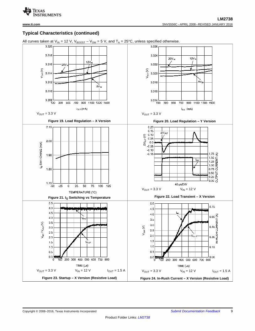
6.6 Typical CharacteristicsAll curves taken at VIN = 12 V, VBOOST – VSW = 5 V, and TA = 25°C, unless specified otherwise.
VOUT = 5 V
Figure 1. Efficiency vs Load Current – X Version
VOUT = 5 V
Figure 2. Efficiency vs Load Current – Y Version
VOUT = 3.3 V
Figure 3. Efficiency vs Load Current – X Version
VOUT = 3.3 V
Figure 4. Efficiency vs Load Current – Y Version
VOUT = 1.5 V
Figure 5. Efficiency vs Load Current – X Version
VOUT = 1.5 V
Figure 6. Efficiency vs Load Current – Y Version

7
LM2738www.ti.com SNVS556C –APRIL 2008–REVISED JANUARY 2016
Product Folder Links: LM2738
Submit Documentation FeedbackCopyright © 2008–2016, Texas Instruments Incorporated
Typical Characteristics (continued)All curves taken at VIN = 12 V, VBOOST – VSW = 5 V, and TA = 25°C, unless specified otherwise.
Figure 7. Oscillator Frequency vs Temperature – X Version Figure 8. Oscillator Frequency vs Temperature – Y Version
VIN = 5 V
Figure 9. Current Limit vs Temperature Figure 10. IQ Non-Switching vs Temperature
Figure 11. VFB vs Temperature Figure 12. RDSON vs Temperature

8
LM2738SNVS556C –APRIL 2008–REVISED JANUARY 2016 www.ti.com
Product Folder Links: LM2738
Submit Documentation Feedback Copyright © 2008–2016, Texas Instruments Incorporated
Typical Characteristics (continued)All curves taken at VIN = 12 V, VBOOST – VSW = 5 V, and TA = 25°C, unless specified otherwise.
VOUT = 1.5 V IOUT = 750 mA
Figure 13. Line Regulation – X Version
VOUT = 1.5 V IOUT = 750 mA
Figure 14. Line Regulation – Y Version
VOUT = 3.3 V IOUT = 750 mA
Figure 15. Line Regulation – X Version
VOUT = 3.3 V IOUT = 750 mA
Figure 16. Line Regulation – Y Version
VOUT = 1.5 V
Figure 17. Load Regulation – X Version
VOUT = 1.5 V
Figure 18. Load Regulation – Y Version
9
LM2738www.ti.com SNVS556C –APRIL 2008–REVISED JANUARY 2016
Product Folder Links: LM2738
Submit Documentation FeedbackCopyright © 2008–2016, Texas Instruments Incorporated
Typical Characteristics (continued)All curves taken at VIN = 12 V, VBOOST – VSW = 5 V, and TA = 25°C, unless specified otherwise.
VOUT = 3.3 V
Figure 19. Load Regulation – X Version
VOUT = 3.3 V
Figure 20. Load Regulation – Y Version
Figure 21. IQ Switching vs Temperature
VOUT = 3.3 V VIN = 12 V
Figure 22. Load Transient – X Version
VOUT = 3.3 V VIN = 12 V IOUT = 1.5 A
Figure 23. Startup – X Version (Resistive Load)
VOUT = 3.3 V VIN = 12 V IOUT = 1.5 A
Figure 24. In-Rush Current – X Version (Resistive Load)

0
0
VIN
VD
TON
t
t
InductorCurrent
D = TON/TSW
VSW
TOFF
TSWIL
IPK
SWVoltage
10
LM2738SNVS556C –APRIL 2008–REVISED JANUARY 2016 www.ti.com
Product Folder Links: LM2738
Submit Documentation Feedback Copyright © 2008–2016, Texas Instruments Incorporated
7 Detailed Description
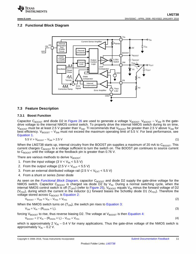
7.1 OverviewThe LM2738 is a constant frequency PWM buck regulator device that delivers a 1.5-A load current. The regulatorhas a preset switching frequency of either 550 kHz (LM2738Y) or 1.6 MHz (LM2738X). These high frequenciesallow the LM2738 to operate with small surface-mount capacitors and inductors, resulting in DC-DC convertersthat require a minimum amount of board space. The LM2738 is internally compensated, so it is simple to use andrequires few external components. The LM2738 uses current-mode control to regulate the output voltage.
The LM2738 supplies a regulated output voltage by switching the internal NMOS control switch at constantfrequency and variable duty cycle. A switching cycle begins at the falling edge of the reset pulse generated bythe internal oscillator. When this pulse goes low, the output control logic turns on the internal NMOS controlswitch. During this on time, the SW pin voltage (VSW) swings up to approximately VIN, and the inductor current(IL) increases with a linear slope. IL is measured by the current-sense amplifier, which generates an outputproportional to the switch current. The sense signal is summed with the regulator’s corrective ramp andcompared to the error amplifier’s output, which is proportional to the difference between the feedback voltageand VREF. When the PWM comparator output goes high, the output switch turns off until the next switching cyclebegins. During the switch off-time, inductor current discharges through Schottky diode D1, which forces the SWpin to swing below ground by the forward voltage (VD) of the catch diode. The regulator loop adjusts the dutycycle (D) to maintain a constant output voltage. See Functional Block Diagram and Figure 25.
Figure 25. LM2738 Waveforms of SW Pin Voltage and Inductor Current
L
R1
R2
D1
D2
BOOST
OutputControlLogic
CurrentLimit
ThermalShutdown
UnderVoltageLockout
Corrective Ramp
ResetPulse
PWMComparator
Current-Sense AmplifierRSENSE
+
+
InternalRegulator
andEnableCircuit
Oscillator
Driver 0.25:Switch
InternalCompensation
SW
EN
FB
GND
Error Amplifier -+ VREF
0.8V
COUT
ON
OFF
VBOOST
IL
VSW
+-
CBOOST
VOUT
CIN
VIN
VIN
ISENSE
+-
+ -
+- 0.93V
-+
OVPComparator
ErrorSignal
11
LM2738www.ti.com SNVS556C –APRIL 2008–REVISED JANUARY 2016
Product Folder Links: LM2738
Submit Documentation FeedbackCopyright © 2008–2016, Texas Instruments Incorporated
7.2 Functional Block Diagram
7.3 Feature Description
7.3.1 Boost FunctionCapacitor CBOOST and diode D2 in Figure 26 are used to generate a voltage VBOOST. VBOOST – VSW is the gate-drive voltage to the internal NMOS control switch. To properly drive the internal NMOS switch during its on time,VBOOST must be at least 2.5 V greater than VSW. TI recommends that VBOOST be greater than 2.5 V above VSW forbest efficiency. VBOOST – VSW must not exceed the maximum operating limit of 5.5 V. For best performance, seeEquation 1.
5.5 V > VBOOST – VSW > 2.5 V (1)
When the LM2738 starts up, internal circuitry from the BOOST pin supplies a maximum of 20 mA to CBOOST. Thiscurrent charges CBOOST to a voltage sufficient to turn the switch on. The BOOST pin continues to source currentto CBOOST until the voltage at the feedback pin is greater than 0.76 V.
There are various methods to derive VBOOST:1. From the input voltage (3 V < VIN < 5.5 V)2. From the output voltage (2.5 V < VOUT < 5.5 V)3. From an external distributed voltage rail (2.5 V < VEXT < 5.5 V)4. From a shunt or series Zener diode
As seen on the Functional Block Diagram, capacitor CBOOST and diode D2 supply the gate-drive voltage for theNMOS switch. Capacitor CBOOST is charged via diode D2 by VIN. During a normal switching cycle, when theinternal NMOS control switch is off (TOFF) (refer to Figure 25), VBOOST equals VIN minus the forward voltage of D2(VFD2), during which the current in the inductor (L) forward biases the Schottky diode D1 (VFD1). Therefore thevoltage stored across CBOOST is Equation 2:
VBOOST – VSW = VIN – VFD2 + VFD1 (2)
When the NMOS switch turns on (TON), the switch pin rises to Equation 3:VSW = VIN – (RDSON × IL), (3)
forcing VBOOST to rise, thus reverse biasing D2. The voltage at VBOOST is then Equation 4:VBOOST = 2 VIN – (RDSON × IL) – VFD2 + VFD1 (4)
which is approximately 2 VIN – 0.4 V for many applications. Thus the gate-drive voltage of the NMOS switch isapproximately VIN – 0.2 V.
LM2738
VIN BOOST
SWGND
CBOOST
L
D1
D2
D3
VBOOST
VOUT
VIN
CIN
COUT
LM2738
BOOST
SWGND
L
D1
D2
COUT
CBOOST
VOUT
CIN
VINVIN
VBOOST
12
LM2738SNVS556C –APRIL 2008–REVISED JANUARY 2016 www.ti.com
Product Folder Links: LM2738
Submit Documentation Feedback Copyright © 2008–2016, Texas Instruments Incorporated
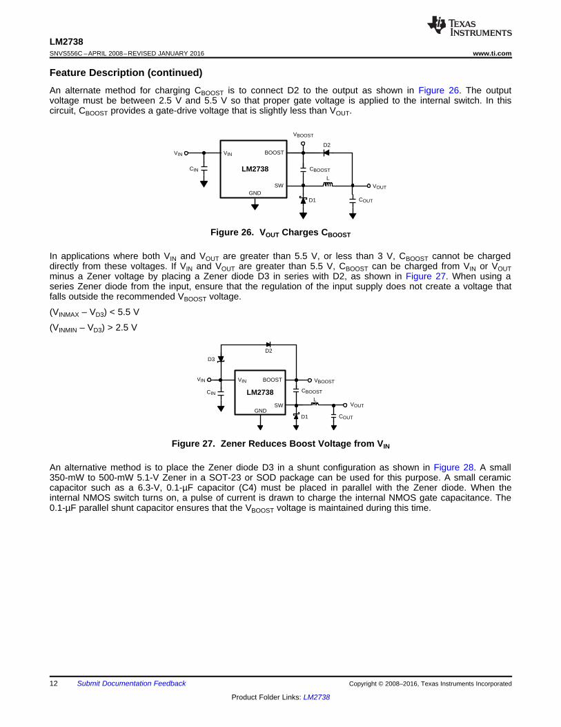
Feature Description (continued)An alternate method for charging CBOOST is to connect D2 to the output as shown in Figure 26. The outputvoltage must be between 2.5 V and 5.5 V so that proper gate voltage is applied to the internal switch. In thiscircuit, CBOOST provides a gate-drive voltage that is slightly less than VOUT.
Figure 26. VOUT Charges CBOOST
In applications where both VIN and VOUT are greater than 5.5 V, or less than 3 V, CBOOST cannot be chargeddirectly from these voltages. If VIN and VOUT are greater than 5.5 V, CBOOST can be charged from VIN or VOUTminus a Zener voltage by placing a Zener diode D3 in series with D2, as shown in Figure 27. When using aseries Zener diode from the input, ensure that the regulation of the input supply does not create a voltage thatfalls outside the recommended VBOOST voltage.
(VINMAX – VD3) < 5.5 V
(VINMIN – VD3) > 2.5 V
Figure 27. Zener Reduces Boost Voltage from VIN
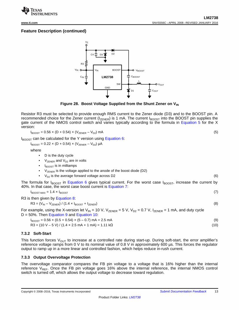
An alternative method is to place the Zener diode D3 in a shunt configuration as shown in Figure 28. A small350-mW to 500-mW 5.1-V Zener in a SOT-23 or SOD package can be used for this purpose. A small ceramiccapacitor such as a 6.3-V, 0.1-µF capacitor (C4) must be placed in parallel with the Zener diode. When theinternal NMOS switch turns on, a pulse of current is drawn to charge the internal NMOS gate capacitance. The0.1-µF parallel shunt capacitor ensures that the VBOOST voltage is maintained during this time.
LM2738
VIN BOOST
SW
GND
L
D1
D2D3
R3
C4
VBOOST
CBOOST
VZ
VOUT
COUT
VIN
CIN
13
LM2738www.ti.com SNVS556C –APRIL 2008–REVISED JANUARY 2016
Product Folder Links: LM2738
Submit Documentation FeedbackCopyright © 2008–2016, Texas Instruments Incorporated
Feature Description (continued)
Figure 28. Boost Voltage Supplied from the Shunt Zener on VIN
Resistor R3 must be selected to provide enough RMS current to the Zener diode (D3) and to the BOOST pin. Arecommended choice for the Zener current (IZENER) is 1 mA. The current IBOOST into the BOOST pin supplies thegate current of the NMOS control switch and varies typically according to the formula in Equation 5 for the Xversion:
IBOOST = 0.56 × (D + 0.54) × (VZENER – VD2) mA (5)
IBOOST can be calculated for the Y version using Equation 6:IBOOST = 0.22 × (D + 0.54) × (VZENER – VD2) µA
where• D is the duty cycle• VZENER and VD2 are in volts• IBOOST is in milliamps• VZENER is the voltage applied to the anode of the boost diode (D2)• VD2 is the average forward voltage across D2 (6)
The formula for IBOOST in Equation 6 gives typical current. For the worst case IBOOST, increase the current by40%. In that case, the worst case boost current is Equation 7:
IBOOST-MAX = 1.4 × IBOOST (7)
R3 is then given by Equation 8:R3 = (VIN – VZENER) / (1.4 × IBOOST + IZENER) (8)
For example, using the X-version let VIN = 10 V, VZENER = 5 V, VD2 = 0.7 V, IZENER = 1 mA, and duty cycleD = 50%. Then Equation 9 and Equation 10:
IBOOST = 0.56 × (0.5 + 0.54) × (5 – 0.7) mA = 2.5 mA (9)R3 = (10 V – 5 V) / (1.4 × 2.5 mA + 1 mA) = 1.11 kΩ (10)
7.3.2 Soft-StartThis function forces VOUT to increase at a controlled rate during start-up. During soft-start, the error amplifier’sreference voltage ramps from 0 V to its nominal value of 0.8 V in approximately 600 µs. This forces the regulatoroutput to ramp up in a more linear and controlled fashion, which helps reduce in-rush current.
7.3.3 Output Overvoltage ProtectionThe overvoltage comparator compares the FB pin voltage to a voltage that is 16% higher than the internalreference VREF. Once the FB pin voltage goes 16% above the internal reference, the internal NMOS controlswitch is turned off, which allows the output voltage to decrease toward regulation.

14
LM2738SNVS556C –APRIL 2008–REVISED JANUARY 2016 www.ti.com
Product Folder Links: LM2738
Submit Documentation Feedback Copyright © 2008–2016, Texas Instruments Incorporated
Feature Description (continued)7.3.4 Undervoltage LockoutUndervoltage lockout (UVLO) prevents the LM2738 from operating until the input voltage exceeds 2.7 V (typical).
The UVLO threshold has approximately 400 mV of hysteresis, so the part operates until VIN drops below 2.3 V(typical). Hysteresis prevents the part from turning off during power up if the VIN ramp-up is non-monotonic.
7.3.5 Current LimitThe LM2738 uses cycle-by-cycle current limiting to protect the output switch. During each switching cycle, acurrent limit comparator detects if the output switch current exceeds 2.9 A (typical), and turns off the switch untilthe next switching cycle begins.
7.3.6 Thermal ShutdownThermal shutdown limits total power dissipation by turning off the output switch when the device junctiontemperature exceeds 165°C. After thermal shutdown occurs, the output switch doesn’t turn on until the junctiontemperature drops to approximately 150°C.
7.4 Device Functional Modes
7.4.1 Enable Pin and Shutdown ModeThe LM2738 has a shutdown mode that is controlled by the enable pin (EN). When a logic low voltage is appliedto EN, the part is in shutdown mode, and its quiescent current drops to typically 400 nA. The voltage at this pinmust never exceed VIN + 0.3 V.

LM2738
VIN VIN
EN
BOOST
SW
FBGND
VOUT
C3L1
C2
R1
R2
D1
D2
ON
OFF
C1 R3
15
LM2738www.ti.com SNVS556C –APRIL 2008–REVISED JANUARY 2016
Product Folder Links: LM2738
Submit Documentation FeedbackCopyright © 2008–2016, Texas Instruments Incorporated
8 Application and Implementation
NOTEInformation in the following applications sections is not part of the TI componentspecification, and TI does not warrant its accuracy or completeness. TI’s customers areresponsible for determining suitability of components for their purposes. Customers mustvalidate and test their design implementation to confirm system functionality.
8.1 Application InformationThe LM2738 operates over a wide range of conditions, which is limited by the ON time of the device. Figure 29shows the recommended operating area for the X version at the full load (1.5 A) and at 25°C ambienttemperature. The Y version of the LM2738 operates at a lower frequency, and therefore operates over the entirerange of operating voltages.
Figure 29. LM2738X – 1.6 MHz (25°C, Load = 1.5 A)
8.2 Typical Applications
8.2.1 LM2738X Circuit Example 1
Figure 30. LM2738X (1.6 MHz)VBOOST Derived from VIN
5 V to 1.5 V/1.5 A
8.2.1.1 Design RequirementsThe device must be able to operate at any voltage within the Recommended Operating Conditions. The loadcurrent must be defined to properly size the inductor, input, and output capacitors. The inductor must be able tosupport the full expected load current as well as the peak current generated from load transients and start-up.

IN OUT L
S
V V 2 i
L DT
- D=
D =VO + VD
VIN + VD - VSW
D =VO
VIN
16
LM2738SNVS556C –APRIL 2008–REVISED JANUARY 2016 www.ti.com
Product Folder Links: LM2738
Submit Documentation Feedback Copyright © 2008–2016, Texas Instruments Incorporated
Typical Applications (continued)8.2.1.2 Detailed Design Procedure
Table 1. Bill of Materials for Figure 30PART ID PART VALUE PART NUMBER MANUFACTURERU1 1.5-A Buck Regulator LM2738X Texas InstrumentsC1, Input Cap 10 µF, 6.3 V, X5R C3216X5ROJ106M TDKC2, Output Cap 22 µF, 6.3 V, X5R C3216X5ROJ226M TDKC3, Boost Cap 0.1 uF, 16 V, X7R C1005X7R1C104K TDKD1, Catch Diode 0.34 VF Schottky 1.5 A, 30 V CRS08 ToshibaD2, Boost Diode 1 VF at 100-mA Diode BAT54WS Diodes, Inc.L1 2.2 µH, 1.9 A, MSS5131-222ML CoilcraftR1 8.87 kΩ, 1% CRCW06038871F VishayR2 10.2 kΩ, 1% CRCW06031022F VishayR3 100 kΩ, 1% CRCW06031003F Vishay
8.2.1.2.1 Inductor Selection
The duty cycle (D) can be approximated quickly using the ratio of output voltage (VO) to input voltage (VIN), usingEquation 11:
(11)
The catch diode (D1) forward voltage drop and the voltage drop across the internal NMOS switch must beincluded to calculate a more accurate duty cycle. Calculate D by using Equation 12:
(12)
VSW can be approximated by Equation 13:VSW = IOUT × RDSON (13)
The diode forward drop (VD) can range from 0.3 V to 0.7 V depending on the quality of the diode. The lower theVD, the higher the operating efficiency of the converter. The inductor value determines the output ripple current.Lower inductor values decrease the size of the inductor, but increase the output ripple current. An increase in theinductor value decreases the output ripple current.
One must ensure that the minimum current limit (2 A) is not exceeded, so the peak current in the inductor mustbe calculated. The peak current (ILPK) in the inductor is calculated by Equation 14 and Equation 15:
ILPK = IOUT + ΔiL (14)
Figure 31. Inductor Current
(15)
In general in Equation 16,ΔiL = 0.1 × (IOUT) → 0.2 × (IOUT) (16)

RMS _IN OUTI I D(1 D)= ´ -
2 LRMS _IN OUT
2 iI D I (1 D)
3
Dé ù- +ê ú
ë û
S
S
1T
f=
2
2 LCOND OUT DSON
OUT
i1P (I D) 1 R
3 I
æ öæ öDç ÷= ´ + ´ç ÷ç ÷è øè ø
17
LM2738www.ti.com SNVS556C –APRIL 2008–REVISED JANUARY 2016
Product Folder Links: LM2738
Submit Documentation FeedbackCopyright © 2008–2016, Texas Instruments Incorporated
Typical Applications (continued)If ΔiL = 33.3% of 1.5 A, the peak current in the inductor is 2 A. The minimum specified current limit over alloperating conditions is 2 A. One can either reduce ΔiL, or make the engineering judgment that zero margin issafe enough. The typical current limit is 2.9 A.
The LM2738 operates at frequencies allowing the use of ceramic output capacitors without compromisingtransient response. Ceramic capacitors allow higher inductor ripple without significantly increasing output ripple.See the Output Capacitor section for more details on calculating output voltage ripple. Now that the ripple currentis determined, the inductance is calculated by Equation 17:
where
• (17)
When selecting an inductor, make sure that it is capable of supporting the peak output current without saturating.Inductor saturation results in a sudden reduction in inductance and prevents the regulator from operatingcorrectly. Because of the speed of the internal current limit, the peak current of the inductor need only bespecified for the required maximum output current. For example, if the designed maximum output current is 1 Aand the peak current is 1.25 A, the inductor must be specified with a saturation current limit of > 1.25 A. There isno must specify the saturation or peak current of the inductor at the 2.9-A typical switch current limit. Because ofthe operating frequency of the LM2738, ferrite based inductors are preferred to minimize core losses. Thispresents little restriction because of the variety of ferrite-based inductors available. Lastly, inductors with lowerseries resistance (RDCR) provide better operating efficiency. For recommended inductors see LM2738X CircuitExample 1.
8.2.1.2.2 Input Capacitor
An input capacitor is necessary to ensure that VIN does not drop excessively during switching transients. Theprimary specifications of the input capacitor are capacitance, voltage, RMS current rating, and equivalent seriesinductance (ESL). The recommended input capacitance is 10 µF. The input voltage rating is specifically stated bythe capacitor manufacturer. Make sure to check any recommended deratings and also verify if there is anysignificant change in capacitance at the operating input voltage and the operating temperature. The inputcapacitor maximum RMS input current rating (IRMS-IN) must be greater than Equation 18:
(18)
Neglecting inductor ripple simplifies Equation 18 to Equation 19:
(19)
Equation 19 shows that maximum RMS capacitor current occurs when D = 0.5. Always calculate the RMS at thepoint where the duty cycle D is closest to 0.5. The ESL of an input capacitor is usually determined by theeffective cross-sectional area of the current path. A large leaded capacitor has high ESL and a 0805 ceramic-chip capacitor has very low ESL. At the operating frequencies of the LM2738, leaded capacitors may have anESL so large that the resulting impedance (2πfL) is higher than that required to provide stable operation. As aresult, surface-mount capacitors are strongly recommended.
Sanyo POSCAP, Tantalum or Niobium, Panasonic SP, and multilayer ceramic capacitors (MLCC) are all goodchoices for both input and output capacitors and have very low ESL. For MLCCs, TI recommends using X7R orX5R type capacitors due to their tolerance and temperature characteristics. Consult the capacitor manufacturer'sdata sheets to see how rated capacitance varies over operating conditions.
8.2.1.2.3 Output Capacitor
The output capacitor is selected based upon the desired output ripple and transient response. The initial currentof a load transient is provided mainly by the output capacitor. The output ripple of the converter is Equation 20:

OUT D
IN D SW
V VD
V V V
+
=
+ -
OUT
OUT LOSS
P
P Ph =
+
OUT
IN
P
Ph =
O
REF
VR1 1 R2
V
æ ö= - ´ç ÷
è ø
OUT L ESR
SW OUT
1V I R
8 F C
æ öD = D +ç ÷
´ ´è ø
18
LM2738SNVS556C –APRIL 2008–REVISED JANUARY 2016 www.ti.com
Product Folder Links: LM2738
Submit Documentation Feedback Copyright © 2008–2016, Texas Instruments Incorporated
Typical Applications (continued)
(20)
When using MLCCs, the equivalent series resistance (ESR) is typically so low that the capacitive ripple maydominate. When this occurs, the output ripple is approximately sinusoidal and 90° phase shifted from theswitching action. Given the availability and quality of MLCCs and the expected output voltage of designs usingthe LM2738, there is really no must review any other capacitor technologies. Another benefit of ceramiccapacitors is the ability to bypass high-frequency noise. A certain amount of switching edge noise couplesthrough parasitic capacitances in the inductor to the output. A ceramic capacitor bypasses this noise while atantalum capacitor does not. Since the output capacitor is one of the two external components that control thestability of the regulator control loop, most applications require a minimum of 22 µF of output capacitance.Capacitance, in general, is often increased when operating at lower duty cycles. Refer to the Circuit Examples forsuggested output capacitances of common applications. Like the input capacitor, recommended multilayerceramic capacitors are X7R or X5R types.
8.2.1.2.4 Catch Diode
The catch diode (D1) conducts during the switch off time. A Schottky diode is recommended for its fast switchingtimes and low forward voltage drop. The catch diode must be chosen so that its current rating is greater thanEquation 21:
ID1 = IOUT × (1-D) (21)
The reverse breakdown rating of the diode must be at least the maximum input voltage plus appropriate margin.To improve efficiency, choose a Schottky diode with a low forward-voltage drop.
8.2.1.2.5 Output Voltage
The output voltage is set using Equation 22 and Equation 23 where R2 is connected between the FB pin andGND, and R1 is connected between VO and the FB pin. A good value for R2 is 10 kΩ. When designing a unitygain converter (VO = 0.8 V), R1 must be between 0 Ω and 100 Ω, and R2 must not be loaded.
(22)VREF = 0.80 V (23)
8.2.1.2.6 Calculating Efficiency and Junction Temperature
The complete LM2738 DC-DC converter efficiency can be calculated by Equation 24 or Equation 25:
(24)
or,
(25)
Calculations for determining the most significant power losses are shown in Equation 26. Other losses totalingless than 2% are not discussed.
Power loss (PLOSS) is the sum of two basic types of losses in the converter: switching and conduction.Conduction losses usually dominate at higher output loads, whereas switching losses remain relatively fixed anddominate at lower output loads. The first step in determining the losses is to calculate the duty cycle (D):
(26)
VSW is the voltage drop across the internal NFET when it is on, and is equal to Equation 27:VSW = IOUT × RDSON (27)

2
2 LCOND OUT DSON
OUT
i1P (I D) 1 R
3 I
æ öæ öDç ÷= ´ + ´ ç ÷ç ÷è øè ø
OUT D DCR
IN D DCR SW
V V VD
V V V V
+ +
=
+ + -
19
LM2738www.ti.com SNVS556C –APRIL 2008–REVISED JANUARY 2016
Product Folder Links: LM2738
Submit Documentation FeedbackCopyright © 2008–2016, Texas Instruments Incorporated
Typical Applications (continued)VD is the forward voltage drop across the Schottky catch diode. It can be obtained from the diode manufacturer'sdata sheet Electrical Characteristics section. If the voltage drop across the inductor (VDCR) is accounted for, theequation becomes Equation 28:
(28)
The conduction losses in the free-wheeling Schottky diode are calculated by Equation 29:PDIODE = VD × IOUT × (1-D) (29)
Often this is the single most significant power loss in the circuit. Care must be taken to choose a Schottky diodethat has a low forward-voltage drop.
Another significant external power loss is the conduction loss in the output inductor. The equation can besimplified to Equation 30:
PIND = IOUT2 × RDCR (30)
The LM2738 conduction loss is mainly associated with the internal NFET switch in Equation 31:
(31)
If the inductor ripple current is fairly small, the conduction losses can be simplified to Equation 32:PCOND = IOUT
2 × RDSON × D (32)
Switching losses are also associated with the internal NFET switch. They occur during the switch on and offtransition periods, where voltages and currents overlap resulting in power loss. The simplest means to determinethis loss is to empirically measure the rise and fall times (10% to 90%) of the switch at the switch node.
Switching Power Loss is calculated as follows in Equation 33, Equation 34, and Equation 35:PSWR = 1/2(VIN × IOUT × FSW × TRISE) (33)PSWF = 1/2(VIN × IOUT × FSW × TFALL) (34)PSW = PSWR + PSWF (35)
Another loss is the power required for operation of the internal circuitry in Equation 36:PQ = IQ × VIN (36)
IQ is the quiescent operating current, and is typically around 1.9 mA for the 0.55-MHz frequency option.
Table 2 lists the power losses for a typical application, and in Equation 37, Equation 38, and Equation 39.
Table 2. Typical Configuration and Power Loss CalculationPARAMETER VALUE POWER PARAMETER CALCULATED POWER
VIN 12 V — —VOUT 3.3 V POUT 4.125 WIOUT 1.25 A — —VD 0.34 V PDIODE 317 mW
FSW 550 kHz — —IQ 1.9 mA PQ 22.8 mW
TRISE 8 nS PSWR 33 mWTFALL 8 nS PSWF 33 mW
RDS(ON) 275 mΩ PCOND 118 mWINDDCR 70 mΩ PIND 110 mW
D 0.275 PLOSS 634 mWη 86.7% PINTERNAL 207 mW
20
LM2738SNVS556C –APRIL 2008–REVISED JANUARY 2016 www.ti.com
Product Folder Links: LM2738
Submit Documentation Feedback Copyright © 2008–2016, Texas Instruments Incorporated
ΣPCOND + PSW + PDIODE + PIND + PQ = PLOSS (37)ΣPCOND + PSWF + PSWR + PQ = PINTERNAL (38)PINTERNAL = 207 mW (39)
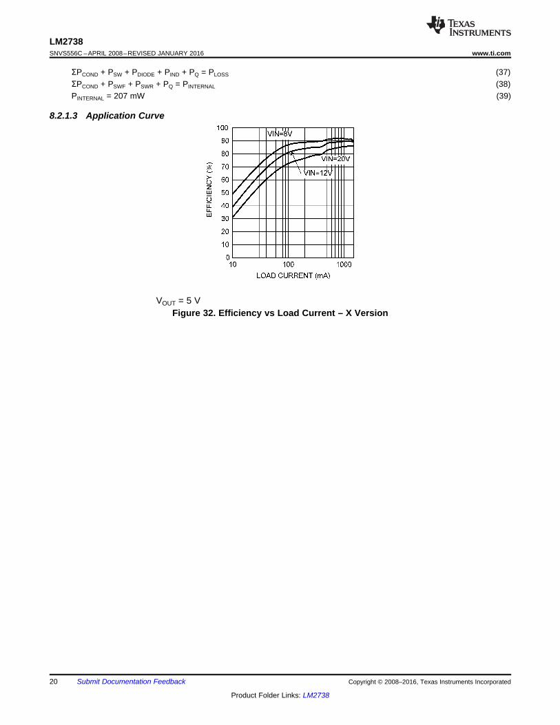
8.2.1.3 Application Curve
VOUT = 5 VFigure 32. Efficiency vs Load Current – X Version
21
LM2738www.ti.com SNVS556C –APRIL 2008–REVISED JANUARY 2016
Product Folder Links: LM2738
Submit Documentation FeedbackCopyright © 2008–2016, Texas Instruments Incorporated
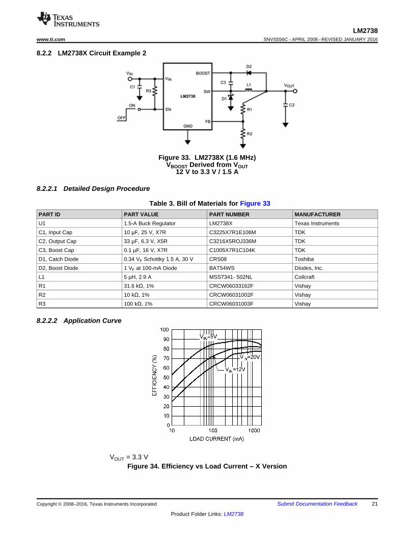
8.2.2 LM2738X Circuit Example 2
Figure 33. LM2738X (1.6 MHz)VBOOST Derived from VOUT
12 V to 3.3 V / 1.5 A
8.2.2.1 Detailed Design Procedure
Table 3. Bill of Materials for Figure 33PART ID PART VALUE PART NUMBER MANUFACTURERU1 1.5-A Buck Regulator LM2738X Texas InstrumentsC1, Input Cap 10 µF, 25 V, X7R C3225X7R1E106M TDKC2, Output Cap 33 µF, 6.3 V, X5R C3216X5ROJ336M TDKC3, Boost Cap 0.1 µF, 16 V, X7R C1005X7R1C104K TDKD1, Catch Diode 0.34 VF Schottky 1.5 A, 30 V CRS08 ToshibaD2, Boost Diode 1 VF at 100-mA Diode BAT54WS Diodes, Inc.L1 5 µH, 2.9 A MSS7341- 502NL CoilcraftR1 31.6 kΩ, 1% CRCW06033162F VishayR2 10 kΩ, 1% CRCW06031002F VishayR3 100 kΩ, 1% CRCW06031003F Vishay
8.2.2.2 Application Curve
VOUT = 3.3 VFigure 34. Efficiency vs Load Current – X Version
LM2738
VIN VIN
EN
BOOST
SW
FBGND
VOUT
C3 L1
C2
R1
R2
D1
D2
ON
OFF
D3C4
R4
C1 R3
22
LM2738SNVS556C –APRIL 2008–REVISED JANUARY 2016 www.ti.com
Product Folder Links: LM2738
Submit Documentation Feedback Copyright © 2008–2016, Texas Instruments Incorporated
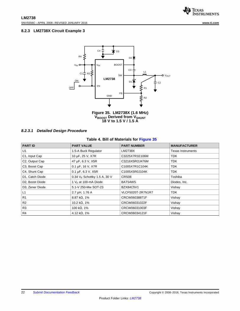
8.2.3 LM2738X Circuit Example 3
Figure 35. LM2738X (1.6 MHz)VBOOST Derived from VSHUNT
18 V to 1.5 V / 1.5 A
8.2.3.1 Detailed Design Procedure
Table 4. Bill of Materials for Figure 35PART ID PART VALUE PART NUMBER MANUFACTURERU1 1.5-A Buck Regulator LM2738X Texas InstrumentsC1, Input Cap 10 µF, 25 V, X7R C3225X7R1E106M TDKC2, Output Cap 47 µF, 6.3 V, X5R C3216X5ROJ476M TDKC3, Boost Cap 0.1 µF, 16 V, X7R C1005X7R1C104K TDKC4, Shunt Cap 0.1 µF, 6.3 V, X5R C1005X5R0J104K TDKD1, Catch Diode 0.34 VF Schottky 1.5 A, 30 V CRS08 ToshibaD2, Boost Diode 1 VF at 100-mA Diode BAT54WS Diodes, Inc.D3, Zener Diode 5.1-V 250-Mw SOT-23 BZX84C5V1 VishayL1 2.7 µH, 1.76 A VLCF5020T-2R7N1R7 TDKR1 8.87 kΩ, 1% CRCW06038871F VishayR2 10.2 kΩ, 1% CRCW06031022F VishayR3 100 kΩ, 1% CRCW06031003F VishayR4 4.12 kΩ, 1% CRCW06034121F Vishay

LM2738
VIN VIN
EN
BOOST
SW
FBGND
VOUT
C3L1
C2
R1
R2
D1 ON
OFF
D2D3
C1 R3
23
LM2738www.ti.com SNVS556C –APRIL 2008–REVISED JANUARY 2016
Product Folder Links: LM2738
Submit Documentation FeedbackCopyright © 2008–2016, Texas Instruments Incorporated
8.2.3.2 Application Curve
VOUT = 1.5 VFigure 36. Efficiency vs Load Current – X Version
8.2.4 LM2738X Circuit Example 4
Figure 37. LM2738X (1.6 MHz)VBOOST Derived from Series Zener Diode (VIN)
15 V to 1.5 V / 1.5 A
8.2.4.1 Detailed Design Procedure
Table 5. Bill of Materials for Figure 37PART ID PART VALUE PART NUMBER MANUFACTURERU1 1.5-A Buck Regulator LM2738X Texas InstrumentsC1, Input Cap 10 µF, 25 V, X7R C3225X7R1E106M TDKC2, Output Cap 47 µF, 6.3 V, X5R C3216X5ROJ476M TDKC3, Boost Cap 0.1 µF, 16 V, X7R C1005X7R1C104K TDKD1, Catch Diode 0.34 VF Schottky 1.5 A, 30 V CRS08 ToshibaD2, Boost Diode 1 VF at 100-mA Diode BAT54WS Diodes, Inc.D3, Zener Diode 11-V 350-Mw SOT-23 BZX84C11T Diodes, Inc.L1 3.3 µH, 3.5 A MSS7341-332NL CoilcraftR1 8.87 kΩ, 1% CRCW06038871F VishayR2 10.2 kΩ, 1% CRCW06031022F VishayR3 100 kΩ, 1% CRCW06031003F Vishay
LM2738
VIN VIN
EN
BOOST
SW
FBGND
VOUT
C3L1
C2
R1
R2
D1 ON
OFF
D2 D3
C1 R3
24
LM2738SNVS556C –APRIL 2008–REVISED JANUARY 2016 www.ti.com
Product Folder Links: LM2738
Submit Documentation Feedback Copyright © 2008–2016, Texas Instruments Incorporated
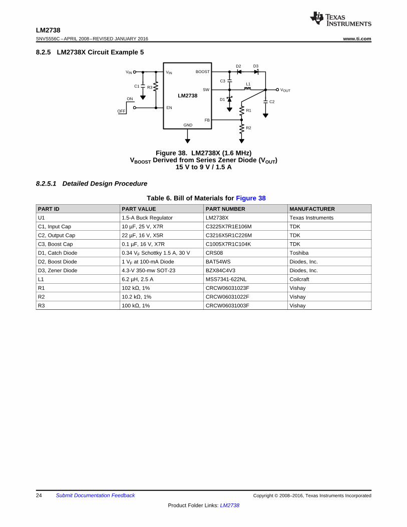
8.2.5 LM2738X Circuit Example 5
Figure 38. LM2738X (1.6 MHz)VBOOST Derived from Series Zener Diode (VOUT)
15 V to 9 V / 1.5 A
8.2.5.1 Detailed Design Procedure
Table 6. Bill of Materials for Figure 38PART ID PART VALUE PART NUMBER MANUFACTURERU1 1.5-A Buck Regulator LM2738X Texas InstrumentsC1, Input Cap 10 µF, 25 V, X7R C3225X7R1E106M TDKC2, Output Cap 22 µF, 16 V, X5R C3216X5R1C226M TDKC3, Boost Cap 0.1 µF, 16 V, X7R C1005X7R1C104K TDKD1, Catch Diode 0.34 VF Schottky 1.5 A, 30 V CRS08 ToshibaD2, Boost Diode 1 VF at 100-mA Diode BAT54WS Diodes, Inc.D3, Zener Diode 4.3-V 350-mw SOT-23 BZX84C4V3 Diodes, Inc.L1 6.2 µH, 2.5 A MSS7341-622NL CoilcraftR1 102 kΩ, 1% CRCW06031023F VishayR2 10.2 kΩ, 1% CRCW06031022F VishayR3 100 kΩ, 1% CRCW06031003F Vishay
LM2738
VIN VIN
EN
BOOST
SW
FBGND
VOUT
C3L1
C2
R1
R2
D1
D2
ON
OFF
C1 R3
25
LM2738www.ti.com SNVS556C –APRIL 2008–REVISED JANUARY 2016
Product Folder Links: LM2738
Submit Documentation FeedbackCopyright © 2008–2016, Texas Instruments Incorporated
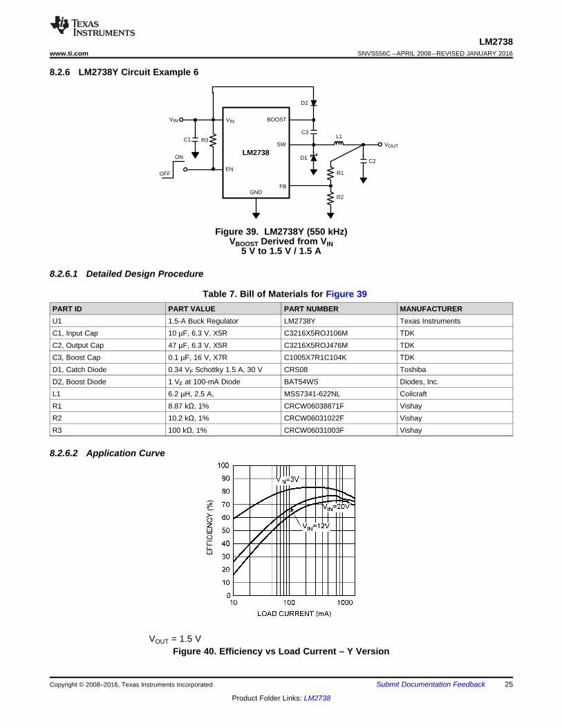
8.2.6 LM2738Y Circuit Example 6
Figure 39. LM2738Y (550 kHz)VBOOST Derived from VIN
5 V to 1.5 V / 1.5 A
8.2.6.1 Detailed Design Procedure
Table 7. Bill of Materials for Figure 39PART ID PART VALUE PART NUMBER MANUFACTURERU1 1.5-A Buck Regulator LM2738Y Texas InstrumentsC1, Input Cap 10 µF, 6.3 V, X5R C3216X5ROJ106M TDKC2, Output Cap 47 µF, 6.3 V, X5R C3216X5ROJ476M TDKC3, Boost Cap 0.1 µF, 16 V, X7R C1005X7R1C104K TDKD1, Catch Diode 0.34 VF Schottky 1.5 A, 30 V CRS08 ToshibaD2, Boost Diode 1 VF at 100-mA Diode BAT54WS Diodes, Inc.L1 6.2 µH, 2.5 A, MSS7341-622NL CoilcraftR1 8.87 kΩ, 1% CRCW06038871F VishayR2 10.2 kΩ, 1% CRCW06031022F VishayR3 100 kΩ, 1% CRCW06031003F Vishay
8.2.6.2 Application Curve
VOUT = 1.5 VFigure 40. Efficiency vs Load Current – Y Version

26
LM2738SNVS556C –APRIL 2008–REVISED JANUARY 2016 www.ti.com
Product Folder Links: LM2738
Submit Documentation Feedback Copyright © 2008–2016, Texas Instruments Incorporated
8.2.7 LM2738Y Circuit Example 7
Figure 41. LM2738Y (550 kHz)VBOOST Derived from VOUT
12 V to 3.3 V / 1.5 A
8.2.7.1 Detailed Design Procedure
Table 8. Bill of Materials for Figure 41PART ID PART VALUE PART NUMBER MANUFACTURERU1 1.5-A Buck Regulator LM2738Y Texas InstrumentsC1, Input Cap 10 µF, 25 V, X7R C3225X7R1E106M TDKC2, Output Cap 47 µF, 6.3 V, X5R C3216X5ROJ476M TDKC3, Boost Cap 0.1 µF, 16 V, X7R C1005X7R1C104K TDKD1, Catch Diode 0.34 VF Schottky 1.5 A, 30 V CRS08 ToshibaD2, Boost Diode 1 VF at 100-mA Diode BAT54WS VishayL1 12 µH, 1.7 A, MSS7341-123NL CoilcraftR1 31.6 kΩ, 1% CRCW06033162F VishayR2 10 kΩ, 1% CRCW06031002F VishayR3 100 kΩ, 1% CRCW06031003F Vishay
8.2.7.2 Application Curve
VOUT = 3.3 VFigure 42. Efficiency vs Load Current – Y Version

LM2738
VIN VIN
EN
BOOST
SW
FBGND
VOUT
C3 L1
C2
R1
R2
D1
D2
ON
OFF
D3C4
R4
C1 R3
27
LM2738www.ti.com SNVS556C –APRIL 2008–REVISED JANUARY 2016
Product Folder Links: LM2738
Submit Documentation FeedbackCopyright © 2008–2016, Texas Instruments Incorporated
8.2.8 LM2738Y Circuit Example 8
Figure 43. LM2738Y (550 kHz)VBOOST Derived from VSHUNT
18 V to 1.5 V / 1.5 A
8.2.8.1 Detailed Design Procedure
Table 9. Bill of Materials for Figure 43PART ID PART VALUE PART NUMBER MANUFACTURERU1 1.5-A Buck Regulator LM2738Y Texas InstrumentsC1, Input Cap 10 µF, 25 V, X7R C3225X7R1E106M TDKC2, Output Cap (47 µF, 6.3 V, X5R) × 2 = 94 µF C3216X5ROJ476M TDKC3, Boost Cap 0.1 µF, 16 V, X7R C1005X7R1C104K TDKC4, Shunt Cap 0.1 µF, 6.3 V, X5R C1005X5R0J104K TDKD1, Catch Diode 0.34 VF Schottky 1.5 A, 30 V CRS08 ToshibaD2, Boost Diode 1 VF at 100-mA Diode BAT54WS Diodes, Inc.D3, Zener Diode 5.1-V 250-Mw SOT-23 BZX84C5V1 VishayL1 8.7 µH, 2.2 A MSS7341-872NL CoilcraftR1 8.87 kΩ, 1% CRCW06038871F VishayR2 10.2 kΩ, 1% CRCW06031022F VishayR3 100 kΩ, 1% CRCW06031003F VishayR4 4.12 kΩ, 1% CRCW06034121F Vishay

LM2738
VIN VIN
EN
BOOST
SW
FBGND
VOUT
C3L1
C2
R1
R2
D1 ON
OFF
D2D3
C1 R3
28
LM2738SNVS556C –APRIL 2008–REVISED JANUARY 2016 www.ti.com
Product Folder Links: LM2738
Submit Documentation Feedback Copyright © 2008–2016, Texas Instruments Incorporated
8.2.8.2 Application Curve
VOUT = 1.5 VFigure 44. Efficiency vs Load Current – Y Version
8.2.9 LM2738Y Circuit Example 9
Figure 45. LM2738Y (550 kHz)VBOOST Derived from Series Zener Diode (VIN)
15 V to 1.5 V / 1.5 A
8.2.9.1 Detailed Design Procedure
Table 10. Bill of Materials for Figure 45PART ID PART VALUE PART NUMBER MANUFACTURERU1 1.5-A Buck Regulator LM2738Y Texas InstrumentsC1, Input Cap 10 µF, 25 V, X7R C3225X7R1E106M TDKC2, Output Cap (47 µF, 6.3 V, X5R) × 2 = 94 µF C3216X5ROJ476M TDKC3, Boost Cap 0.1 µF, 16 V, X7R C1005X7R1C104K TDKD1, Catch Diode 0.34 VF Schottky 1.5 A, 30 V CRS08 ToshibaD2, Boost Diode 1 VF at 100-mA Diode BAT54WS Diodes, Inc.D3, Zener Diode 11-V 350-Mw SOT-23 BZX84C11T Diodes, Inc.L1 8.7 µH, 2.2 A MSS7341-872NL CoilcraftR1 8.87 kΩ, 1% CRCW06038871F VishayR2 10.2 kΩ, 1% CRCW06031022F VishayR3 100 kΩ, 1% CRCW06031003F Vishay
LM2738
VIN VIN
EN
BOOST
SW
FBGND
VOUT
C3L1
C2
R1
R2
D1 ON
OFF
D2 D3
C1 R3
29
LM2738www.ti.com SNVS556C –APRIL 2008–REVISED JANUARY 2016
Product Folder Links: LM2738
Submit Documentation FeedbackCopyright © 2008–2016, Texas Instruments Incorporated
8.2.9.2 Application Curve
VOUT = 1.5 VFigure 46. Efficiency vs Load Current – Y Version
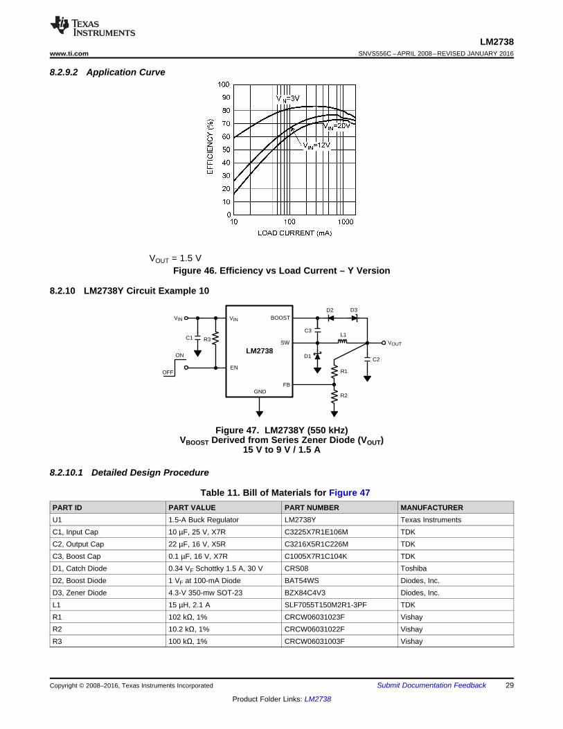
8.2.10 LM2738Y Circuit Example 10
Figure 47. LM2738Y (550 kHz)VBOOST Derived from Series Zener Diode (VOUT)
15 V to 9 V / 1.5 A
8.2.10.1 Detailed Design Procedure
Table 11. Bill of Materials for Figure 47PART ID PART VALUE PART NUMBER MANUFACTURERU1 1.5-A Buck Regulator LM2738Y Texas InstrumentsC1, Input Cap 10 µF, 25 V, X7R C3225X7R1E106M TDKC2, Output Cap 22 µF, 16 V, X5R C3216X5R1C226M TDKC3, Boost Cap 0.1 µF, 16 V, X7R C1005X7R1C104K TDKD1, Catch Diode 0.34 VF Schottky 1.5 A, 30 V CRS08 ToshibaD2, Boost Diode 1 VF at 100-mA Diode BAT54WS Diodes, Inc.D3, Zener Diode 4.3-V 350-mw SOT-23 BZX84C4V3 Diodes, Inc.L1 15 µH, 2.1 A SLF7055T150M2R1-3PF TDKR1 102 kΩ, 1% CRCW06031023F VishayR2 10.2 kΩ, 1% CRCW06031022F VishayR3 100 kΩ, 1% CRCW06031003F Vishay

30
LM2738SNVS556C –APRIL 2008–REVISED JANUARY 2016 www.ti.com
Product Folder Links: LM2738
Submit Documentation Feedback Copyright © 2008–2016, Texas Instruments Incorporated
9 Power Supply RecommendationsThe input voltage is rated as 3 V to 20 V. Care must be taken in certain circuit configurations, such as whenVBOOST is derived from VIN, where the requirement that VBOOST – VSW is less than 5.5 V must be observed. Alsofor best efficiency, VBOOST must be at least 2.5 V above VSW. The voltage on the enable (EN) pin must notexceed VIN by more than 0.3 V.
10 Layout
10.1 Layout GuidelinesWhen planning layout there are a few things to consider when trying to achieve a clean, regulated output. Themost important consideration is the close coupling of the GND connections of the input capacitor and the catchdiode D1. These ground ends must be close to one another and be connected to the GND plane with at leasttwo through-holes. Place these components as close as possible to the device. Next in importance is the locationof the GND connection of the output capacitor, which must be near the GND connections of CIN and D1. Theremust be a continuous ground plane on the bottom layer of a two-layer board except under the switching nodeisland. The FB pin is a high-impedance node, and take care to make the FB trace short to avoid noise pickupand inaccurate regulation. The feedback resistors must be placed as close to the device as possible, with theGND of R1 placed as close to the GND of the device as possible. The VOUT trace to R2 must be routed awayfrom the inductor and any other traces that are switching. High AC currents flow through the VIN, SW, and VOUTtraces, so they must be as short and wide as possible. However, making the traces wide increases radiatednoise, so the designer must make this trade-off. Radiated noise can be decreased by choosing a shieldedinductor. The remaining components must also be placed as close to the device as possible. See AN-1229SIMPLE SWITCHER® PCB Layout Guidelines (SNVA054) for further considerations, and the LM2738 demoboard as an example of a four-layer layout.
10.1.1 WSON Package
Figure 48. Internal WSON Connection
For certain high power applications, the PCB land may be modified to a dog-bone shape (see Figure 49). Byincreasing the size of ground plane, and adding thermal vias, the RθJA for the application can be reduced.
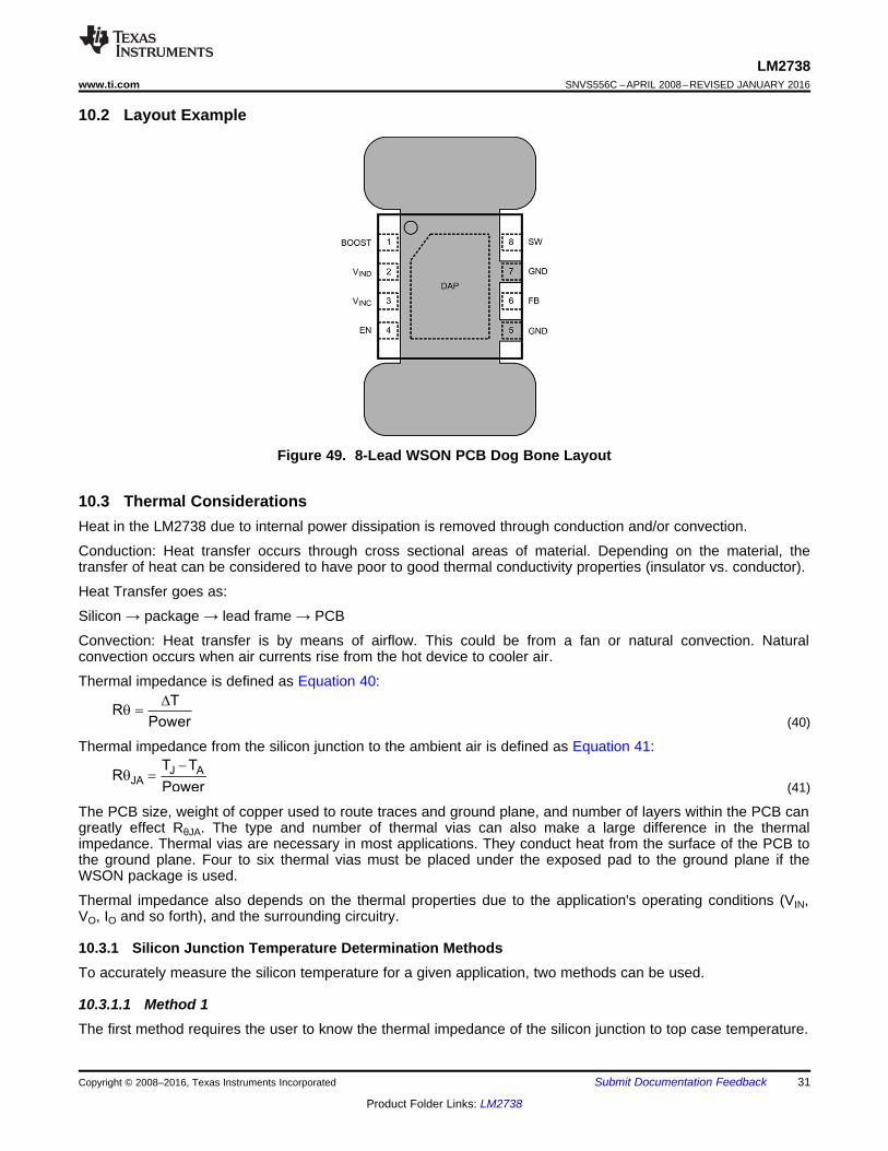
J AJA
T TR
Power
-q =
TR
Power
Dq =
31
LM2738www.ti.com SNVS556C –APRIL 2008–REVISED JANUARY 2016
Product Folder Links: LM2738
Submit Documentation FeedbackCopyright © 2008–2016, Texas Instruments Incorporated
10.2 Layout Example
Figure 49. 8-Lead WSON PCB Dog Bone Layout
10.3 Thermal ConsiderationsHeat in the LM2738 due to internal power dissipation is removed through conduction and/or convection.
Conduction: Heat transfer occurs through cross sectional areas of material. Depending on the material, thetransfer of heat can be considered to have poor to good thermal conductivity properties (insulator vs. conductor).
Heat Transfer goes as:
Silicon → package → lead frame → PCB
Convection: Heat transfer is by means of airflow. This could be from a fan or natural convection. Naturalconvection occurs when air currents rise from the hot device to cooler air.
Thermal impedance is defined as Equation 40:
(40)
Thermal impedance from the silicon junction to the ambient air is defined as Equation 41:
(41)
The PCB size, weight of copper used to route traces and ground plane, and number of layers within the PCB cangreatly effect RθJA. The type and number of thermal vias can also make a large difference in the thermalimpedance. Thermal vias are necessary in most applications. They conduct heat from the surface of the PCB tothe ground plane. Four to six thermal vias must be placed under the exposed pad to the ground plane if theWSON package is used.
Thermal impedance also depends on the thermal properties due to the application's operating conditions (VIN,VO, IO and so forth), and the surrounding circuitry.
10.3.1 Silicon Junction Temperature Determination MethodsTo accurately measure the silicon temperature for a given application, two methods can be used.
10.3.1.1 Method 1The first method requires the user to know the thermal impedance of the silicon junction to top case temperature.

JA
165 C 144 CR 102 C/W
207 mW
° - °q = = °
AJA
INTERNAL
165 TR
P
°-q =
J CJC
T TR
Power
-F =
32
LM2738SNVS556C –APRIL 2008–REVISED JANUARY 2016 www.ti.com
Product Folder Links: LM2738
Submit Documentation Feedback Copyright © 2008–2016, Texas Instruments Incorporated
Thermal Considerations (continued)To clarify:
RθJC is the thermal impedance from all six sides of a device package to silicon junction.
In this data sheet RΦJC is used, allowing the user to measure top case temperature with a small thermocoupleattached to the top case.
RΦJC is approximately 30°C/W for the 8-pin WSON package with the exposed pad. With the internal dissipationfrom the efficiency calculation given previously, and the case temperature, RΦJC can be empirically measured onthe bench as Equation 42.
(42)
Therefore in Equation 43:Tj = (RΦJC × PLOSS) + TC (43)
From the previous example, shows Equation 44 and Equation 45:Tj = (RΦJC × PINTERNAL) + TC (44)Tj = 30°C/W × 0.207 W + TC (45)
10.3.1.2 Method 2The second method can give a very accurate silicon junction temperature.
The first step is to determine RθJA of the application. The LM2738 has overtemperature protection circuitry. Whenthe silicon temperature reaches 165°C, the device stops switching. The protection circuitry has a hysteresis ofabout 15°C. Once the silicon temperature has decreased to approximately 150°C, the device starts to switchagain. Knowing this, the RθJA for any application can be characterized during the early stages of the design onemay calculate the RθJA by placing the PCB circuit into a thermal chamber. Raise the ambient temperature in thegiven working application until the circuit enters thermal shutdown. If the SW pin is monitored, it is obvious whenthe internal NFET stops switching, indicating a junction temperature of 165°C. Knowing the internal powerdissipation from the above equations, the junction temperature and the ambient temperature RθJA can bedetermined with Equation 46.
(46)
Once RθJA is determined, the maximum ambient temperature allowed for a desired junction temperature can becalculated.
An example of calculating RθJA for an application using the Texas Instruments LM2738 WSON demonstrationboard is shown in Equation 48.
The four-layer PCB is constructed using FR4 with ½ oz copper traces. The copper ground plane is on the bottomlayer. The ground plane is accessed by two vias. The board measures 3 cm × 3 cm. It was placed in an ovenwith no forced airflow. The ambient temperature was raised to 144°C, and at that temperature, the device wentinto thermal shutdown.
From the previous example, Equation 47 and Equation 48 shows:PINTERNAL = 207 mW (47)
(48)
If the junction temperature is kept below 125°C, then the ambient temperature cannot go above 109°C, seen inEquation 49 and Equation 50.
Tj – (RθJA × PLOSS) = TA (49)125°C – (102°C/W × 207 mW) = 104°C (50)

33
LM2738www.ti.com SNVS556C –APRIL 2008–REVISED JANUARY 2016
Product Folder Links: LM2738
Submit Documentation FeedbackCopyright © 2008–2016, Texas Instruments Incorporated
11 Device and Documentation Support
11.1 Device Support
11.1.1 Third-Party Products DisclaimerTI'S PUBLICATION OF INFORMATION REGARDING THIRD-PARTY PRODUCTS OR SERVICES DOES NOTCONSTITUTE AN ENDORSEMENT REGARDING THE SUITABILITY OF SUCH PRODUCTS OR SERVICESOR A WARRANTY, REPRESENTATION OR ENDORSEMENT OF SUCH PRODUCTS OR SERVICES, EITHERALONE OR IN COMBINATION WITH ANY TI PRODUCT OR SERVICE.
11.2 Documentation Support
11.2.1 Related DocumentationFor related documentation see the following:
AN-1229 SIMPLE SWITCHER® PCB Layout Guidelines (SNVA054)
11.3 Community ResourcesThe following links connect to TI community resources. Linked contents are provided "AS IS" by the respectivecontributors. They do not constitute TI specifications and do not necessarily reflect TI's views; see TI's Terms ofUse.
TI E2E™ Online Community TI's Engineer-to-Engineer (E2E) Community. Created to foster collaborationamong engineers. At e2e.ti.com, you can ask questions, share knowledge, explore ideas and helpsolve problems with fellow engineers.
Design Support TI's Design Support Quickly find helpful E2E forums along with design support tools andcontact information for technical support.
11.4 TrademarksPowerPAD, E2E are trademarks of Texas Instruments.All other trademarks are the property of their respective owners.
11.5 Electrostatic Discharge CautionThese devices have limited built-in ESD protection. The leads should be shorted together or the device placed in conductive foamduring storage or handling to prevent electrostatic damage to the MOS gates.
11.6 GlossarySLYZ022 — TI Glossary.
This glossary lists and explains terms, acronyms, and definitions.
12 Mechanical, Packaging, and Orderable InformationThe following pages include mechanical, packaging, and orderable information. This information is the mostcurrent data available for the designated devices. This data is subject to change without notice and revision ofthis document. For browser-based versions of this data sheet, refer to the left-hand navigation.

PACKAGE OPTION ADDENDUM
www.ti.com 8-Oct-2015
Addendum-Page 1
PACKAGING INFORMATION
Orderable Device Status(1)
Package Type PackageDrawing
Pins PackageQty
Eco Plan(2)
Lead/Ball Finish(6)
MSL Peak Temp(3)
Op Temp (°C) Device Marking(4/5)
Samples
LM2738XMY/NOPB ACTIVE MSOP-PowerPAD
DGN 8 1000 Green (RoHS& no Sb/Br)
CU SN Level-1-260C-UNLIM -40 to 125 STDB
LM2738XSD/NOPB ACTIVE WSON NGQ 8 1000 Green (RoHS& no Sb/Br)
CU SN Level-3-260C-168 HR -40 to 125 L237B
LM2738YMY/NOPB ACTIVE MSOP-PowerPAD
DGN 8 1000 Green (RoHS& no Sb/Br)
CU SN Level-1-260C-UNLIM -40 to 125 SJBB
LM2738YSD/NOPB ACTIVE WSON NGQ 8 1000 Green (RoHS& no Sb/Br)
CU SN Level-3-260C-168 HR -40 to 125 L174B
(1) The marketing status values are defined as follows:ACTIVE: Product device recommended for new designs.LIFEBUY: TI has announced that the device will be discontinued, and a lifetime-buy period is in effect.NRND: Not recommended for new designs. Device is in production to support existing customers, but TI does not recommend using this part in a new design.PREVIEW: Device has been announced but is not in production. Samples may or may not be available.OBSOLETE: TI has discontinued the production of the device.
(2) Eco Plan - The planned eco-friendly classification: Pb-Free (RoHS), Pb-Free (RoHS Exempt), or Green (RoHS & no Sb/Br) - please check http://www.ti.com/productcontent for the latest availabilityinformation and additional product content details.TBD: The Pb-Free/Green conversion plan has not been defined.Pb-Free (RoHS): TI's terms "Lead-Free" or "Pb-Free" mean semiconductor products that are compatible with the current RoHS requirements for all 6 substances, including the requirement thatlead not exceed 0.1% by weight in homogeneous materials. Where designed to be soldered at high temperatures, TI Pb-Free products are suitable for use in specified lead-free processes.Pb-Free (RoHS Exempt): This component has a RoHS exemption for either 1) lead-based flip-chip solder bumps used between the die and package, or 2) lead-based die adhesive used betweenthe die and leadframe. The component is otherwise considered Pb-Free (RoHS compatible) as defined above.Green (RoHS & no Sb/Br): TI defines "Green" to mean Pb-Free (RoHS compatible), and free of Bromine (Br) and Antimony (Sb) based flame retardants (Br or Sb do not exceed 0.1% by weightin homogeneous material)
(3) MSL, Peak Temp. - The Moisture Sensitivity Level rating according to the JEDEC industry standard classifications, and peak solder temperature.
(4) There may be additional marking, which relates to the logo, the lot trace code information, or the environmental category on the device.
(5) Multiple Device Markings will be inside parentheses. Only one Device Marking contained in parentheses and separated by a "~" will appear on a device. If a line is indented then it is a continuationof the previous line and the two combined represent the entire Device Marking for that device.
(6) Lead/Ball Finish - Orderable Devices may have multiple material finish options. Finish options are separated by a vertical ruled line. Lead/Ball Finish values may wrap to two lines if the finishvalue exceeds the maximum column width.

PACKAGE OPTION ADDENDUM
www.ti.com 8-Oct-2015
Addendum-Page 2
Important Information and Disclaimer:The information provided on this page represents TI's knowledge and belief as of the date that it is provided. TI bases its knowledge and belief on informationprovided by third parties, and makes no representation or warranty as to the accuracy of such information. Efforts are underway to better integrate information from third parties. TI has taken andcontinues to take reasonable steps to provide representative and accurate information but may not have conducted destructive testing or chemical analysis on incoming materials and chemicals.TI and TI suppliers consider certain information to be proprietary, and thus CAS numbers and other limited information may not be available for release.
In no event shall TI's liability arising out of such information exceed the total purchase price of the TI part(s) at issue in this document sold by TI to Customer on an annual basis.
TAPE AND REEL INFORMATION
*All dimensions are nominal
Device PackageType
PackageDrawing
Pins SPQ ReelDiameter
(mm)
ReelWidth
W1 (mm)
A0(mm)
B0(mm)
K0(mm)
P1(mm)
W(mm)
Pin1Quadrant
LM2738XMY/NOPB MSOP-Power PAD
DGN 8 1000 178.0 12.4 5.3 3.4 1.4 8.0 12.0 Q1
LM2738XSD/NOPB WSON NGQ 8 1000 178.0 12.4 3.3 3.3 1.0 8.0 12.0 Q1
LM2738YMY/NOPB MSOP-Power PAD
DGN 8 1000 178.0 12.4 5.3 3.4 1.4 8.0 12.0 Q1
LM2738YSD/NOPB WSON NGQ 8 1000 178.0 12.4 3.3 3.3 1.0 8.0 12.0 Q1
PACKAGE MATERIALS INFORMATION
www.ti.com 28-Oct-2016
Pack Materials-Page 1

*All dimensions are nominal
Device Package Type Package Drawing Pins SPQ Length (mm) Width (mm) Height (mm)
LM2738XMY/NOPB MSOP-PowerPAD DGN 8 1000 210.0 185.0 35.0
LM2738XSD/NOPB WSON NGQ 8 1000 210.0 185.0 35.0
LM2738YMY/NOPB MSOP-PowerPAD DGN 8 1000 210.0 185.0 35.0
LM2738YSD/NOPB WSON NGQ 8 1000 210.0 185.0 35.0
PACKAGE MATERIALS INFORMATION
www.ti.com 28-Oct-2016
Pack Materials-Page 2

MECHANICAL DATA
DGN0008A
www.ti.com
MUY08A (Rev A)
BOTTOM VIEW

www.ti.com
PACKAGE OUTLINE
C
8X 0.30.2
2 0.1
8X 0.50.3
2X1.5
1.6 0.1
6X 0.5
0.80.7
0.050.00
B 3.12.9
A
3.12.9
(0.1) TYP
WSON - 0.8 mm max heightNGQ0008APLASTIC SMALL OUTLINE - NO LEAD
4214922/A 03/2018
PIN 1 INDEX AREA
SEATING PLANE
0.08 C
1
45
8
PIN 1 ID 0.1 C A B0.05 C
THERMAL PADEXPOSED
9
SYMM
SYMM
NOTES: 1. All linear dimensions are in millimeters. Any dimensions in parenthesis are for reference only. Dimensioning and tolerancing per ASME Y14.5M. 2. This drawing is subject to change without notice. 3. The package thermal pad must be soldered to the printed circuit board for thermal and mechanical performance.
SCALE 4.000
www.ti.com
EXAMPLE BOARD LAYOUT
0.07 MINALL AROUND
0.07 MAXALL AROUND
(1.6)
6X (0.5)
(2.8)
8X (0.25)
8X (0.6)
(2)
(R0.05) TYP ( 0.2) VIATYP
(0.75)
WSON - 0.8 mm max heightNGQ0008APLASTIC SMALL OUTLINE - NO LEAD
4214922/A 03/2018
SYMM
1
45
8
SYMM
LAND PATTERN EXAMPLEEXPOSED METAL SHOWN
SCALE:20X
9
NOTES: (continued) 4. This package is designed to be soldered to a thermal pad on the board. For more information, see Texas Instruments literature number SLUA271 (www.ti.com/lit/slua271).5. Vias are optional depending on application, refer to device data sheet. If any vias are implemented, refer to their locations shown on this view. It is recommended that vias under paste be filled, plugged or tented.
SOLDER MASKOPENINGSOLDER MASK
METAL UNDER
SOLDER MASKDEFINED
EXPOSED METAL
METALSOLDER MASKOPENING
SOLDER MASK DETAILS
NON SOLDER MASKDEFINED
(PREFERRED)
EXPOSED METAL
www.ti.com
EXAMPLE STENCIL DESIGN
8X (0.25)
8X (0.6)
6X (0.5)
(1.79)
(1.47)
(2.8)
(R0.05) TYP
WSON - 0.8 mm max heightNGQ0008APLASTIC SMALL OUTLINE - NO LEAD
4214922/A 03/2018
NOTES: (continued) 6. Laser cutting apertures with trapezoidal walls and rounded corners may offer better paste release. IPC-7525 may have alternate design recommendations.
SOLDER PASTE EXAMPLEBASED ON 0.1 mm THICK STENCIL
EXPOSED PAD 9:
82% PRINTED SOLDER COVERAGE BY AREA UNDER PACKAGESCALE:20X
SYMM
1
45
8
SYMM
METALTYP
9

IMPORTANT NOTICE
Texas Instruments Incorporated (TI) reserves the right to make corrections, enhancements, improvements and other changes to itssemiconductor products and services per JESD46, latest issue, and to discontinue any product or service per JESD48, latest issue. Buyersshould obtain the latest relevant information before placing orders and should verify that such information is current and complete.TI’s published terms of sale for semiconductor products (http://www.ti.com/sc/docs/stdterms.htm) apply to the sale of packaged integratedcircuit products that TI has qualified and released to market. Additional terms may apply to the use or sale of other types of TI products andservices.Reproduction of significant portions of TI information in TI data sheets is permissible only if reproduction is without alteration and isaccompanied by all associated warranties, conditions, limitations, and notices. TI is not responsible or liable for such reproduceddocumentation. Information of third parties may be subject to additional restrictions. Resale of TI products or services with statementsdifferent from or beyond the parameters stated by TI for that product or service voids all express and any implied warranties for theassociated TI product or service and is an unfair and deceptive business practice. TI is not responsible or liable for any such statements.Buyers and others who are developing systems that incorporate TI products (collectively, “Designers”) understand and agree that Designersremain responsible for using their independent analysis, evaluation and judgment in designing their applications and that Designers havefull and exclusive responsibility to assure the safety of Designers' applications and compliance of their applications (and of all TI productsused in or for Designers’ applications) with all applicable regulations, laws and other applicable requirements. Designer represents that, withrespect to their applications, Designer has all the necessary expertise to create and implement safeguards that (1) anticipate dangerousconsequences of failures, (2) monitor failures and their consequences, and (3) lessen the likelihood of failures that might cause harm andtake appropriate actions. Designer agrees that prior to using or distributing any applications that include TI products, Designer willthoroughly test such applications and the functionality of such TI products as used in such applications.TI’s provision of technical, application or other design advice, quality characterization, reliability data or other services or information,including, but not limited to, reference designs and materials relating to evaluation modules, (collectively, “TI Resources”) are intended toassist designers who are developing applications that incorporate TI products; by downloading, accessing or using TI Resources in anyway, Designer (individually or, if Designer is acting on behalf of a company, Designer’s company) agrees to use any particular TI Resourcesolely for this purpose and subject to the terms of this Notice.TI’s provision of TI Resources does not expand or otherwise alter TI’s applicable published warranties or warranty disclaimers for TIproducts, and no additional obligations or liabilities arise from TI providing such TI Resources. TI reserves the right to make corrections,enhancements, improvements and other changes to its TI Resources. TI has not conducted any testing other than that specificallydescribed in the published documentation for a particular TI Resource.Designer is authorized to use, copy and modify any individual TI Resource only in connection with the development of applications thatinclude the TI product(s) identified in such TI Resource. NO OTHER LICENSE, EXPRESS OR IMPLIED, BY ESTOPPEL OR OTHERWISETO ANY OTHER TI INTELLECTUAL PROPERTY RIGHT, AND NO LICENSE TO ANY TECHNOLOGY OR INTELLECTUAL PROPERTYRIGHT OF TI OR ANY THIRD PARTY IS GRANTED HEREIN, including but not limited to any patent right, copyright, mask work right, orother intellectual property right relating to any combination, machine, or process in which TI products or services are used. Informationregarding or referencing third-party products or services does not constitute a license to use such products or services, or a warranty orendorsement thereof. Use of TI Resources may require a license from a third party under the patents or other intellectual property of thethird party, or a license from TI under the patents or other intellectual property of TI.TI RESOURCES ARE PROVIDED “AS IS” AND WITH ALL FAULTS. TI DISCLAIMS ALL OTHER WARRANTIES ORREPRESENTATIONS, EXPRESS OR IMPLIED, REGARDING RESOURCES OR USE THEREOF, INCLUDING BUT NOT LIMITED TOACCURACY OR COMPLETENESS, TITLE, ANY EPIDEMIC FAILURE WARRANTY AND ANY IMPLIED WARRANTIES OFMERCHANTABILITY, FITNESS FOR A PARTICULAR PURPOSE, AND NON-INFRINGEMENT OF ANY THIRD PARTY INTELLECTUALPROPERTY RIGHTS. TI SHALL NOT BE LIABLE FOR AND SHALL NOT DEFEND OR INDEMNIFY DESIGNER AGAINST ANY CLAIM,INCLUDING BUT NOT LIMITED TO ANY INFRINGEMENT CLAIM THAT RELATES TO OR IS BASED ON ANY COMBINATION OFPRODUCTS EVEN IF DESCRIBED IN TI RESOURCES OR OTHERWISE. IN NO EVENT SHALL TI BE LIABLE FOR ANY ACTUAL,DIRECT, SPECIAL, COLLATERAL, INDIRECT, PUNITIVE, INCIDENTAL, CONSEQUENTIAL OR EXEMPLARY DAMAGES INCONNECTION WITH OR ARISING OUT OF TI RESOURCES OR USE THEREOF, AND REGARDLESS OF WHETHER TI HAS BEENADVISED OF THE POSSIBILITY OF SUCH DAMAGES.Unless TI has explicitly designated an individual product as meeting the requirements of a particular industry standard (e.g., ISO/TS 16949and ISO 26262), TI is not responsible for any failure to meet such industry standard requirements.Where TI specifically promotes products as facilitating functional safety or as compliant with industry functional safety standards, suchproducts are intended to help enable customers to design and create their own applications that meet applicable functional safety standardsand requirements. Using products in an application does not by itself establish any safety features in the application. Designers mustensure compliance with safety-related requirements and standards applicable to their applications. Designer may not use any TI products inlife-critical medical equipment unless authorized officers of the parties have executed a special contract specifically governing such use.Life-critical medical equipment is medical equipment where failure of such equipment would cause serious bodily injury or death (e.g., lifesupport, pacemakers, defibrillators, heart pumps, neurostimulators, and implantables). Such equipment includes, without limitation, allmedical devices identified by the U.S. Food and Drug Administration as Class III devices and equivalent classifications outside the U.S.TI may expressly designate certain products as completing a particular qualification (e.g., Q100, Military Grade, or Enhanced Product).Designers agree that it has the necessary expertise to select the product with the appropriate qualification designation for their applicationsand that proper product selection is at Designers’ own risk. Designers are solely responsible for compliance with all legal and regulatoryrequirements in connection with such selection.Designer will fully indemnify TI and its representatives against any damages, costs, losses, and/or liabilities arising out of Designer’s non-compliance with the terms and provisions of this Notice.
Mailing Address: Texas Instruments, Post Office Box 655303, Dallas, Texas 75265Copyright © 2018, Texas Instruments Incorporated