lmh0318 programming guide - texas instruments · 1 kΩto vdd 20 kΩto gnd 11 01 1a 34 1 kΩto vdd...
TRANSCRIPT
Programmer's GuideSNLU183–September 2015
LMH0318 Programming Guide
This document provides a reference for the LMH0318 Reclocker from a programming model perspective.It contains detailed information relating to programming and different configuration options. The intendedaudience includes software as well as hardware engineers working on the system diagnostics and controlsoftware.
The reader should be familiar with the LMH0318 datasheet (SNLS508). In addition to the LMH0318datasheet, all other collateral data related to the LMH0318 Reclocker (application notes, models, etc.), areavailable on the TI website. Alternatively, contact your local Texas Instruments field sales representative.
Contents1 Access Methods ............................................................................................................. 2
1.1 Register Programming via SMBus and SPI Interface.......................................................... 21.2 Register Programming via SPI .................................................................................... 31.3 Register Types ..................................................................................................... 3
2 Initialization Set Up .......................................................................................................... 43 Register Command Syntax ................................................................................................ 54 Device Configuration ....................................................................................................... 6
4.1 Common Device Configuration ................................................................................... 64.2 Common Register Commands ................................................................................... 7
5 Register Tables ............................................................................................................. 195.1 Global Registers................................................................................................... 195.2 Receiver Registers ................................................................................................ 235.3 CDR Registers..................................................................................................... 295.4 Transmitter Registers ............................................................................................. 34
List of Tables
1 LMH0318 Register Initialization ............................................................................................ 42 LMH0318 SMPTE Configuration .......................................................................................... 63 SMPTE Data Rate Selection ............................................................................................... 94 CTLE Boost Setting vs Media Trace Length............................................................................ 105 Global Registers............................................................................................................ 196 Receiver Registers ......................................................................................................... 237 CDR Registers.............................................................................................................. 298 Transmitter Registers ...................................................................................................... 34
1SNLU183–September 2015 LMH0318 Programming GuideSubmit Documentation Feedback
Copyright © 2015, Texas Instruments Incorporated
Access Methods www.ti.com
1 Access MethodsTwo methods are provided for accessing the LMH0318 Registers:• Register control via the Serial Management Bus (SMBus)• Register control via the Serial Parallel Interface (SPI)
In a typical system, either SMBus or SPI access is used to configure and monitor the device status.Unless specified, the register configurations for SPI and SMBus are the same.
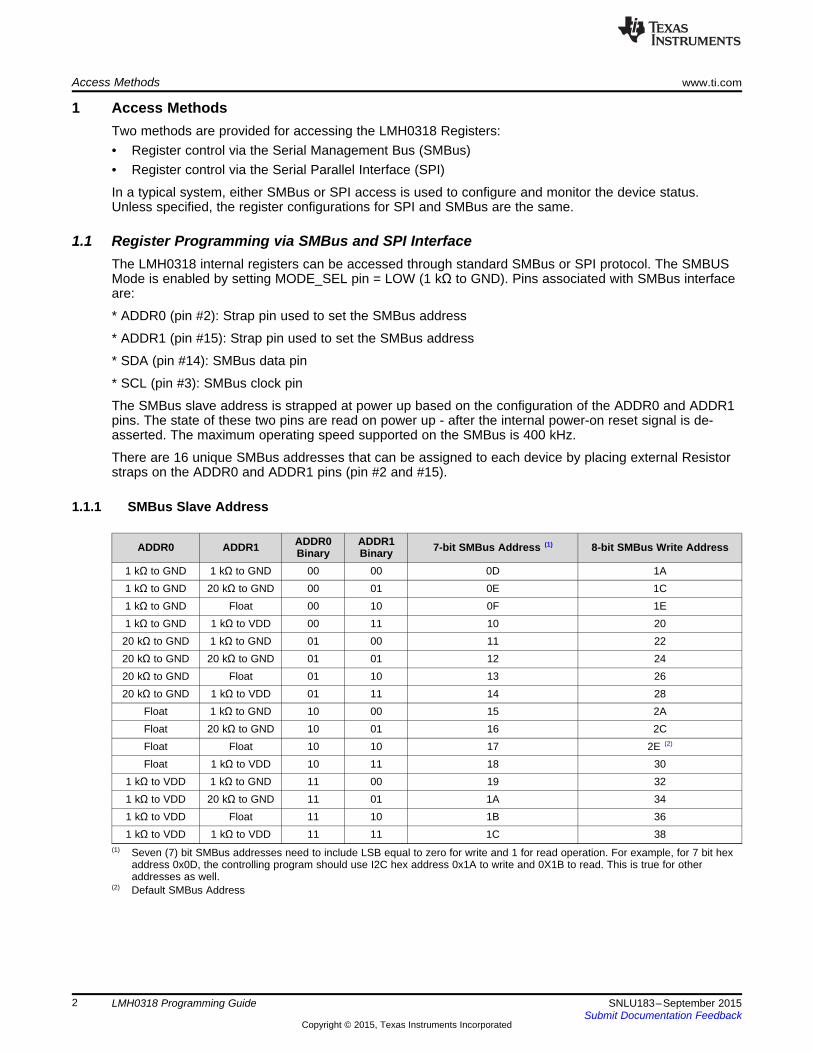
1.1 Register Programming via SMBus and SPI InterfaceThe LMH0318 internal registers can be accessed through standard SMBus or SPI protocol. The SMBUSMode is enabled by setting MODE_SEL pin = LOW (1 kΩ to GND). Pins associated with SMBus interfaceare:
* ADDR0 (pin #2): Strap pin used to set the SMBus address
* ADDR1 (pin #15): Strap pin used to set the SMBus address
* SDA (pin #14): SMBus data pin
* SCL (pin #3): SMBus clock pin
The SMBus slave address is strapped at power up based on the configuration of the ADDR0 and ADDR1pins. The state of these two pins are read on power up - after the internal power-on reset signal is de-asserted. The maximum operating speed supported on the SMBus is 400 kHz.
There are 16 unique SMBus addresses that can be assigned to each device by placing external Resistorstraps on the ADDR0 and ADDR1 pins (pin #2 and #15).
1.1.1 SMBus Slave Address
ADDR0 ADDR1ADDR0 ADDR1 7-bit SMBus Address (1) 8-bit SMBus Write AddressBinary Binary1 kΩ to GND 1 kΩ to GND 00 00 0D 1A1 kΩ to GND 20 kΩ to GND 00 01 0E 1C1 kΩ to GND Float 00 10 0F 1E1 kΩ to GND 1 kΩ to VDD 00 11 10 2020 kΩ to GND 1 kΩ to GND 01 00 11 2220 kΩ to GND 20 kΩ to GND 01 01 12 2420 kΩ to GND Float 01 10 13 2620 kΩ to GND 1 kΩ to VDD 01 11 14 28
Float 1 kΩ to GND 10 00 15 2AFloat 20 kΩ to GND 10 01 16 2CFloat Float 10 10 17 2E (2)
Float 1 kΩ to VDD 10 11 18 301 kΩ to VDD 1 kΩ to GND 11 00 19 321 kΩ to VDD 20 kΩ to GND 11 01 1A 341 kΩ to VDD Float 11 10 1B 361 kΩ to VDD 1 kΩ to VDD 11 11 1C 38
(1) Seven (7) bit SMBus addresses need to include LSB equal to zero for write and 1 for read operation. For example, for 7 bit hexaddress 0x0D, the controlling program should use I2C hex address 0x1A to write and 0X1B to read. This is true for otheraddresses as well.
(2) Default SMBus Address
2 LMH0318 Programming Guide SNLU183–September 2015Submit Documentation Feedback
Copyright © 2015, Texas Instruments Incorporated
www.ti.com Access Methods
1.2 Register Programming via SPIAlternatively, when MODE_Sel is pulled high with 1 kΩ-resistor, the SPI interface is used for deviceconfiguration. Pins associated with the SPI interface are:
* MOSI: Master Output, Slave input (pin#4)
* MISO: Master Input, Slave Output (pin#15)
* SS_N: Slave Select active low (pin#2)
* SPI_SCK: Serial clock output from master (pin#3)
The maximum operating speed supported on the SPI bus is 20 MHz.
1.3 Register TypesThe LMH0318 register set is divided into four groups:• Global Registers- These registers are divided into share and channel registers. Share register define
LMH0318 ID, revision, enabling shared registers. Channels registers are feature specific such asinterrupt status or interrupt mask
• Receiver Registers- These registers are associated with input stage of the device - equalizer boostsetting, signal detect levels and input mux selection.
• Clock Data Recovery (CDR) Registers- These registers control CDR state machine, Eye OpeningMonitor (EOM), and configuration.
• Transmitter Registers- These registers configure output multiplexers and output parameters for OUT0and OUT1.
3SNLU183–September 2015 LMH0318 Programming GuideSubmit Documentation Feedback
Copyright © 2015, Texas Instruments Incorporated
Initialization Set Up www.ti.com
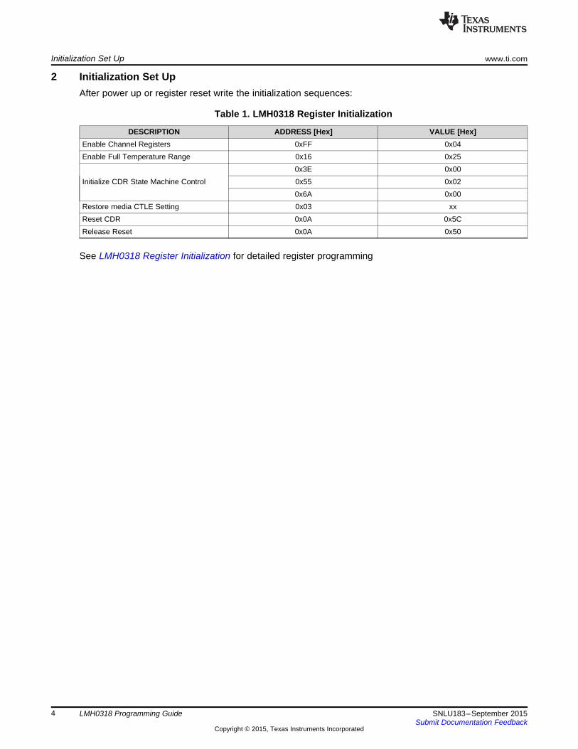
2 Initialization Set UpAfter power up or register reset write the initialization sequences:
Table 1. LMH0318 Register Initialization
DESCRIPTION ADDRESS [Hex] VALUE [Hex]Enable Channel Registers 0xFF 0x04Enable Full Temperature Range 0x16 0x25
0x3E 0x00Initialize CDR State Machine Control 0x55 0x02
0x6A 0x00Restore media CTLE Setting 0x03 xxReset CDR 0x0A 0x5CRelease Reset 0x0A 0x50
See LMH0318 Register Initialization for detailed register programming
4 LMH0318 Programming Guide SNLU183–September 2015Submit Documentation Feedback
Copyright © 2015, Texas Instruments Incorporated

www.ti.com Register Command Syntax
3 Register Command SyntaxUnless otherwise specified, the settings below apply to both SMBus and SPI register programming.Operations are read-modify-write. This requires the register to be read first and modified by applying thespecific bit mask.
Command Syntax:
RAW Register Register Register Mask //CommentsAddress Content
RAW: This defines a Read/Write commandRegister Address: Specifies the register address in hexRegister Content Specifies the value in hex that is going to be writtenRegister Mask: Defines bits within the register content that will be modified//: Text commentExample: RAW In this example, we are setting reg 0x80[0] = 1'b to power down OUT0.80 01 01 0x80[7:1] are not modified since mask = 0x01
RAR Register Register Register Mask //CommentsAddress Content
RAR: Read Only CommandRegister Address: Specifies the register address in hex formatRegister Content Specifies the register content that is being readRegister Mask: Defines the mask for register content. For example, 1 in a mask defines bits
being read//: Characters following // are text commentsExample: RAR Read 0xE2[4] and check if bit 4 is setE2 10 10
● When using SMBus or SPI interface, the host controller may need to set over-ride bit prior to settingthe control bits of a register
● It is recommended to issue CDR Reset and Release after changing register settings that alters CDRstate machine
● See Register Tables for further details on register bit definitions
5SNLU183–September 2015 LMH0318 Programming GuideSubmit Documentation Feedback
Copyright © 2015, Texas Instruments Incorporated

Device Configuration www.ti.com
4 Device ConfigurationThe following sections provide guidance for programming the LMH0318 for certain common applications.
Throughout the rest of the document, macro examples are given to setup the device for differentconfigurations and settings.
4.1 Common Device ConfigurationThe LMH0318 supports SMPTE data rates. Once configured for SMPTE application, the LMH0318 can beoptioned to lock to a selection of data rates and report lock status. The following is an example of commonregister settings for the LMH0318 initialization followed by possible settings to support SMPTE data rates.
Table 2. LMH0318 SMPTE Configuration
COMMAND REGISTER VALUE MASK //Comments//Initialization sequence
RAW FF 04 07 //Select Channel RegistersRAW 16 25 FF //Enable Full Temperature RangeRAW 3E 00 80 //Initialize CDR State Machine ControlRAW 55 02 02RAW 6A 00 FFRAW 03 XX FF //Use the desired CTLE settings. See CTLE Test Mode to determine the
CTLE settingRAW 0A 0C 0C //Reset CDRRAW 0A 00 0C //Release CDR reset
//In default mode, the LMH0318 automatically locks to different SMPTEand ST-2082/1 data rates
RAR 1 1 1 //Read LOS of IN0//Assuming signal is present on IN0, enable IN0 to 75 Ω OUT0 and powerRAW 31 1 3 down 50 Ω OUT1
RAW 2F 00 C0 //Default SMPTE is enabledRAW 0A 0C 0C //Reset CDRRAW 0A 00 0C //Release CDR ResetRAR 02 18 18 //If reg 0x02[4:3] = 11'b, CDR lockedRAW 0C 30 F0 //Setup register 0x0C to enable reg 0x02 to read the VCO divider settingsRAR 02 38 38 //0x02[5:3] Indicates lock ratesRAW 0C 00 F0 //Setup register 0x0C to enable reg 0x02 to read lock indication
6 LMH0318 Programming Guide SNLU183–September 2015Submit Documentation Feedback
Copyright © 2015, Texas Instruments Incorporated
www.ti.com Device Configuration
4.2 Common Register CommandsThe followings macros specify register settings for common operations.
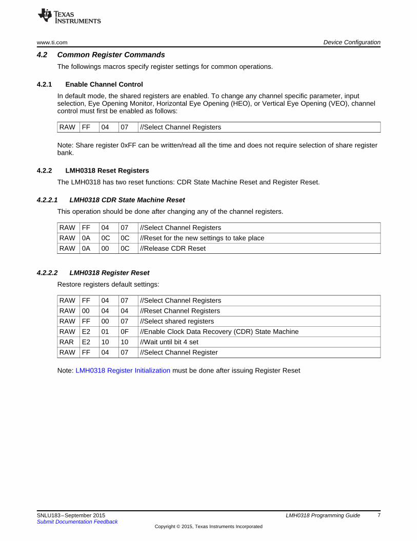
4.2.1 Enable Channel ControlIn default mode, the shared registers are enabled. To change any channel specific parameter, inputselection, Eye Opening Monitor, Horizontal Eye Opening (HEO), or Vertical Eye Opening (VEO), channelcontrol must first be enabled as follows:
RAW FF 04 07 //Select Channel Registers
Note: Share register 0xFF can be written/read all the time and does not require selection of share registerbank.
4.2.2 LMH0318 Reset RegistersThe LMH0318 has two reset functions: CDR State Machine Reset and Register Reset.
4.2.2.1 LMH0318 CDR State Machine ResetThis operation should be done after changing any of the channel registers.
RAW FF 04 07 //Select Channel RegistersRAW 0A 0C 0C //Reset for the new settings to take placeRAW 0A 00 0C //Release CDR Reset
4.2.2.2 LMH0318 Register ResetRestore registers default settings:
RAW FF 04 07 //Select Channel RegistersRAW 00 04 04 //Reset Channel RegistersRAW FF 00 07 //Select shared registersRAW E2 01 0F //Enable Clock Data Recovery (CDR) State MachineRAR E2 10 10 //Wait until bit 4 setRAW FF 04 07 //Select Channel Register
Note: LMH0318 Register Initialization must be done after issuing Register Reset
7SNLU183–September 2015 LMH0318 Programming GuideSubmit Documentation Feedback
Copyright © 2015, Texas Instruments Incorporated
Device Configuration www.ti.com
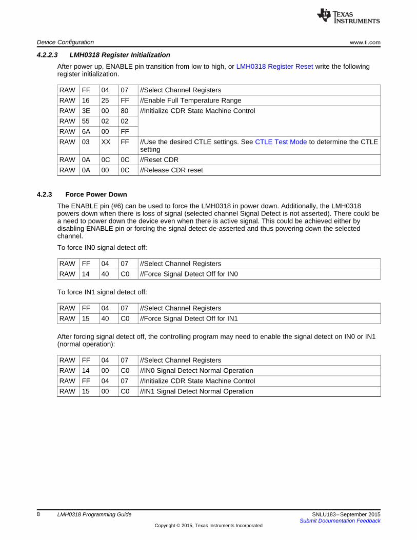
4.2.2.3 LMH0318 Register InitializationAfter power up, ENABLE pin transition from low to high, or LMH0318 Register Reset write the followingregister initialization.
RAW FF 04 07 //Select Channel RegistersRAW 16 25 FF //Enable Full Temperature RangeRAW 3E 00 80 //Initialize CDR State Machine ControlRAW 55 02 02RAW 6A 00 FFRAW 03 XX FF //Use the desired CTLE settings. See CTLE Test Mode to determine the CTLE
settingRAW 0A 0C 0C //Reset CDRRAW 0A 00 0C //Release CDR reset
4.2.3 Force Power DownThe ENABLE pin (#6) can be used to force the LMH0318 in power down. Additionally, the LMH0318powers down when there is loss of signal (selected channel Signal Detect is not asserted). There could bea need to power down the device even when there is active signal. This could be achieved either bydisabling ENABLE pin or forcing the signal detect de-asserted and thus powering down the selectedchannel.
To force IN0 signal detect off:
RAW FF 04 07 //Select Channel RegistersRAW 14 40 C0 //Force Signal Detect Off for IN0
To force IN1 signal detect off:
RAW FF 04 07 //Select Channel RegistersRAW 15 40 C0 //Force Signal Detect Off for IN1
After forcing signal detect off, the controlling program may need to enable the signal detect on IN0 or IN1(normal operation):
RAW FF 04 07 //Select Channel RegistersRAW 14 00 C0 //IN0 Signal Detect Normal OperationRAW FF 04 07 //Initialize CDR State Machine ControlRAW 15 00 C0 //IN1 Signal Detect Normal Operation
8 LMH0318 Programming Guide SNLU183–September 2015Submit Documentation Feedback
Copyright © 2015, Texas Instruments Incorporated
www.ti.com Device Configuration
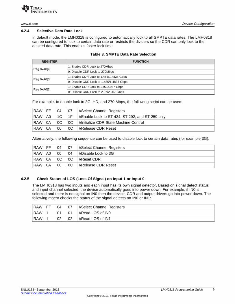
4.2.4 Selective Data Rate LockIn default mode, the LMH0318 is configured to automatically lock to all SMPTE data rates. The LMH0318can be configured to lock to certain data rate or restricts the dividers so the CDR can only lock to thedesired data rate. This enables faster lock time.
Table 3. SMPTE Data Rate Selection
REGISTER FUNCTION1: Enable CDR Lock to 270Mbps
Reg 0xA0[4]0: Disable CDR Lock to 270Mbps1: Enable CDR Lock to 1.485/1.4835 Gbps
Reg 0xA0[3]0: Disable CDR Lock to 1.485/1.4835 Gbps1: Enable CDR Lock to 2.97/2.967 Gbps
Reg 0xA0[2]0: Disable CDR Lock to 2.97/2.967 Gbps
For example, to enable lock to 3G, HD, and 270 Mbps, the following script can be used:
RAW FF 04 07 //Select Channel RegistersRAW A0 1C 1F //Enable Lock to ST 424, ST 292, and ST 259 onlyRAW 0A 0C 0C //Initialize CDR State Machine ControlRAW 0A 00 0C //Release CDR Reset
Alternatively, the following sequence can be used to disable lock to certain data rates (for example 3G):
RAW FF 04 07 //Select Channel RegistersRAW A0 00 04 //Disable Lock to 3GRAW 0A 0C 0C //Reset CDRRAW 0A 00 0C //Release CDR Reset
4.2.5 Check Status of LOS (Loss Of Signal) on Input 1 or Input 0The LMH0318 has two inputs and each input has its own signal detector. Based on signal detect statusand input channel selected, the device automatically goes into power down. For example, if IN0 isselected and there is no signal on IN0 then the device, CDR and output drivers go into power down. Thefollowing macro checks the status of the signal detects on IN0 or IN1:
RAW FF 04 07 //Select Channel RegistersRAW 1 01 01 //Read LOS of IN0RAW 1 02 02 //Read LOS of IN1
9SNLU183–September 2015 LMH0318 Programming GuideSubmit Documentation Feedback
Copyright © 2015, Texas Instruments Incorporated
Device Configuration www.ti.com
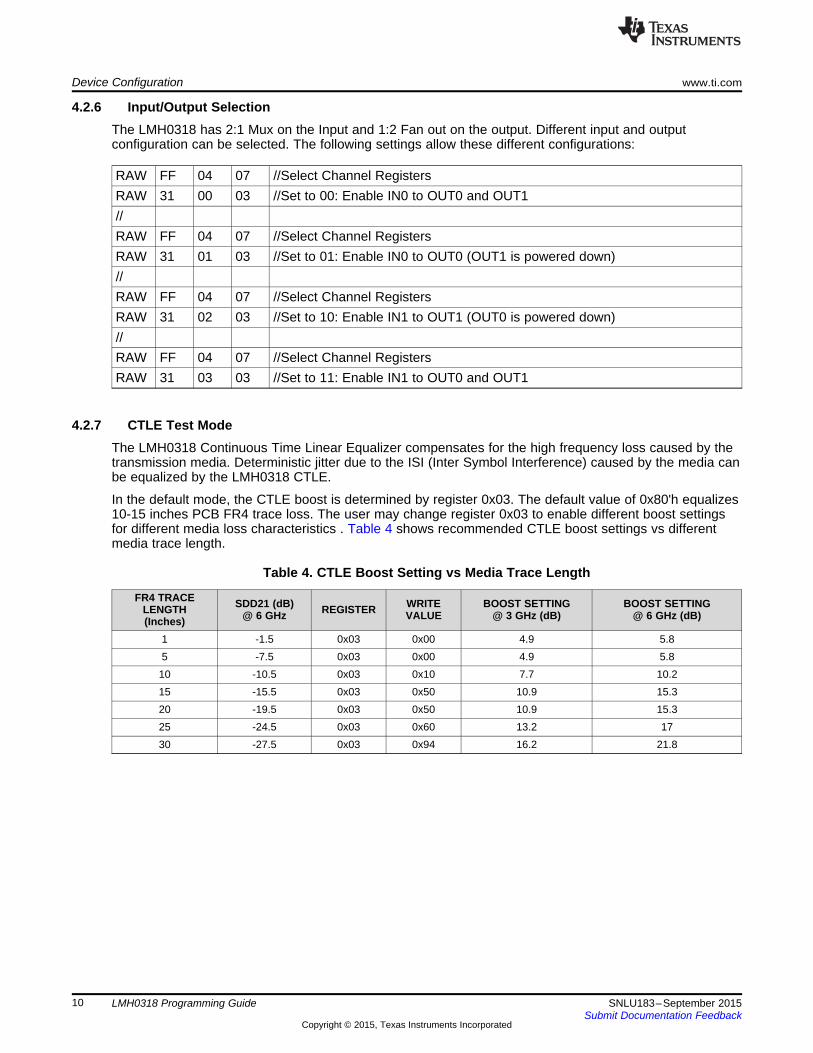
4.2.6 Input/Output SelectionThe LMH0318 has 2:1 Mux on the Input and 1:2 Fan out on the output. Different input and outputconfiguration can be selected. The following settings allow these different configurations:
RAW FF 04 07 //Select Channel RegistersRAW 31 00 03 //Set to 00: Enable IN0 to OUT0 and OUT1//RAW FF 04 07 //Select Channel RegistersRAW 31 01 03 //Set to 01: Enable IN0 to OUT0 (OUT1 is powered down)//RAW FF 04 07 //Select Channel RegistersRAW 31 02 03 //Set to 10: Enable IN1 to OUT1 (OUT0 is powered down)//RAW FF 04 07 //Select Channel RegistersRAW 31 03 03 //Set to 11: Enable IN1 to OUT0 and OUT1
4.2.7 CTLE Test ModeThe LMH0318 Continuous Time Linear Equalizer compensates for the high frequency loss caused by thetransmission media. Deterministic jitter due to the ISI (Inter Symbol Interference) caused by the media canbe equalized by the LMH0318 CTLE.
In the default mode, the CTLE boost is determined by register 0x03. The default value of 0x80'h equalizes10-15 inches PCB FR4 trace loss. The user may change register 0x03 to enable different boost settingsfor different media loss characteristics . Table 4 shows recommended CTLE boost settings vs differentmedia trace length.
Table 4. CTLE Boost Setting vs Media Trace Length
FR4 TRACE SDD21 (dB) WRITE BOOST SETTING BOOST SETTINGLENGTH REGISTER@ 6 GHz VALUE @ 3 GHz (dB) @ 6 GHz (dB)(Inches)1 -1.5 0x03 0x00 4.9 5.85 -7.5 0x03 0x00 4.9 5.810 -10.5 0x03 0x10 7.7 10.215 -15.5 0x03 0x50 10.9 15.320 -19.5 0x03 0x50 10.9 15.325 -24.5 0x03 0x60 13.2 1730 -27.5 0x03 0x94 16.2 21.8
10 LMH0318 Programming Guide SNLU183–September 2015Submit Documentation Feedback
Copyright © 2015, Texas Instruments Incorporated

www.ti.com Device Configuration
For test purpose only, the register sequence below determines the correct CTLE setting. Note, theselected CTLE setting produced by the test mode works for all of the data rates; therefore, this test shouldbe done at the highest data rate. The CTLE compensates for the media not the data rate. Additionally, for3 Gbps or lower, register 0x55 specifies the fixed CTLE setting when operating in CTLE test mode.
RAW FF 04 07 //Select Channel RegistersRAW 2D 00 08 //Disable EQ over-rideRAW 2C 40 40 //Enable VEO scalingRAW 3E 80 80 //Enable HEO/VEORAW 6A 44 FFRAW 31 20 60 //Enable CTLE Test Mode to optimize eye openingRAW 0A 0C 0C //Reset CDR for the new settings to take placeRAW 0A 00 0C //Release CDR ResetRAW 0C 00 F0 //Setup register 0x0C to read lock indicationRAW 02 18 18 //Wait until bits [4:3] = 11'b to indicate CDR lockedRAR 52 xx FF //Read EQ Boost setting and store in xx for normal mode of operationRAW 03 xx FF //Save EQ Boost setting in reg 0x03RAW 2D 08 08 //Enable the device to force EQ Setting from Reg 0x03RAW 31 00 60 //Allow register 0x03 to control CTLE settingRAW 3E 00 80 //Restore initialization settingsRAW 6A 00 FF //Restore initialization settingsRAW 2C 00 40 //Disable VEO scale
11SNLU183–September 2015 LMH0318 Programming GuideSubmit Documentation Feedback
Copyright © 2015, Texas Instruments Incorporated
Device Configuration www.ti.com
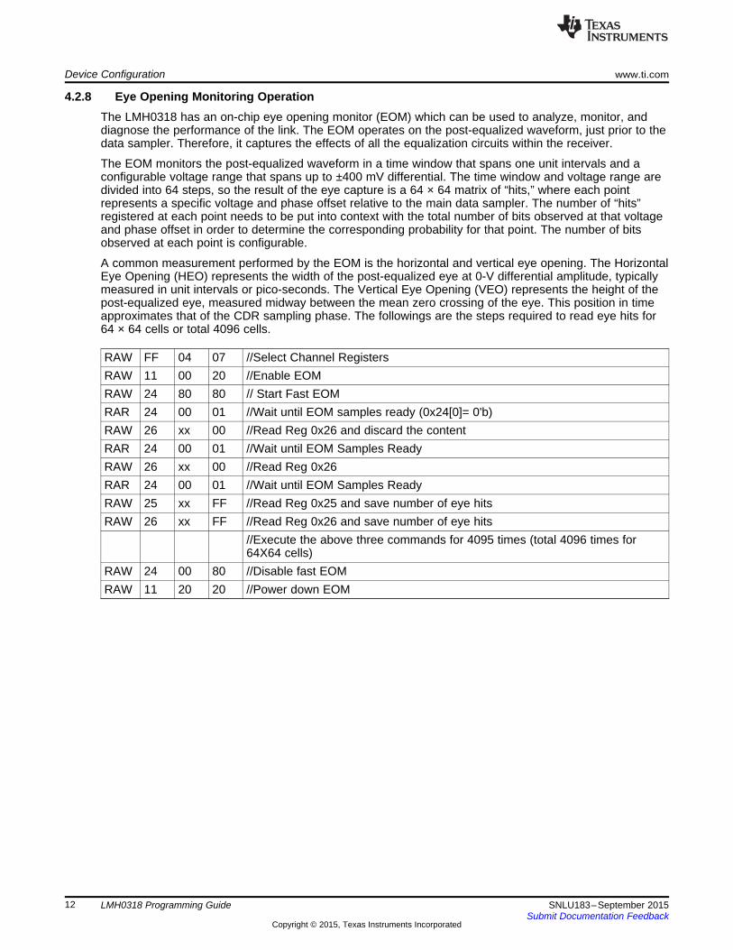
4.2.8 Eye Opening Monitoring OperationThe LMH0318 has an on-chip eye opening monitor (EOM) which can be used to analyze, monitor, anddiagnose the performance of the link. The EOM operates on the post-equalized waveform, just prior to thedata sampler. Therefore, it captures the effects of all the equalization circuits within the receiver.
The EOM monitors the post-equalized waveform in a time window that spans one unit intervals and aconfigurable voltage range that spans up to ±400 mV differential. The time window and voltage range aredivided into 64 steps, so the result of the eye capture is a 64 × 64 matrix of “hits,” where each pointrepresents a specific voltage and phase offset relative to the main data sampler. The number of “hits”registered at each point needs to be put into context with the total number of bits observed at that voltageand phase offset in order to determine the corresponding probability for that point. The number of bitsobserved at each point is configurable.
A common measurement performed by the EOM is the horizontal and vertical eye opening. The HorizontalEye Opening (HEO) represents the width of the post-equalized eye at 0-V differential amplitude, typicallymeasured in unit intervals or pico-seconds. The Vertical Eye Opening (VEO) represents the height of thepost-equalized eye, measured midway between the mean zero crossing of the eye. This position in timeapproximates that of the CDR sampling phase. The followings are the steps required to read eye hits for64 × 64 cells or total 4096 cells.
RAW FF 04 07 //Select Channel RegistersRAW 11 00 20 //Enable EOMRAW 24 80 80 // Start Fast EOMRAR 24 00 01 //Wait until EOM samples ready (0x24[0]= 0'b)RAW 26 xx 00 //Read Reg 0x26 and discard the contentRAR 24 00 01 //Wait until EOM Samples ReadyRAW 26 xx 00 //Read Reg 0x26RAR 24 00 01 //Wait until EOM Samples ReadyRAW 25 xx FF //Read Reg 0x25 and save number of eye hitsRAW 26 xx FF //Read Reg 0x26 and save number of eye hits
//Execute the above three commands for 4095 times (total 4096 times for64X64 cells)
RAW 24 00 80 //Disable fast EOMRAW 11 20 20 //Power down EOM
12 LMH0318 Programming Guide SNLU183–September 2015Submit Documentation Feedback
Copyright © 2015, Texas Instruments Incorporated

www.ti.com Device Configuration
4.2.9 Lock Data Rate IndicationThere could be a need to realize the data rate the device has locked to. In this case, register 0x02[4] isread to make sure the device is locked. Then VCO divisor setting indicates the data rate.
RAW FF 04 07 //Select Channel RegistersRAW 0C 00 F0 //Setup register 0x0c to read lock indication bit 4RAW 02 18 18 //Wait until bit 4 is set indicating device is lockedRAW 0C 30 F0 //Setup register 0x0C to read the VCO divider settingRAR 02 38 38 //Read divider settings
// 02[5-3] = 010'b 2.97 Gbps// 02[5-3] = 011'b 1.485 Gbps// 02[5-3] = 100'b 270Mbps
RAW 0C 00 F0 //Setup the default value for Reg 0x0C
4.2.10 Read Horizontal and Vertical Eye OpeningThe LMH0318 produces two readings to indicate line signal quality: The Horizontal Eye Opening (HEO)and the Vertical Eye Opening (VEO) are indications of signal quality. These parameters can be read bythe host processor or the LMH0318 can be optioned to cause interrupt if HEO/VEO reach a threshold.
To convert the HEO reading to Unit Interval (UI) eye opening, we need to divide the HEO reading, indecimal, to 64.HEO = (Decimal Reg0x27)/64For example, if the HEO reading is 0x31 (49 decimal) then the HEO UI eye opening would be49/64=0.77UI. This means the HEO is about 77% open.
Similarly, VEO has 64 steps as well. The chip automatically covers differential peak to peak value from +/-100mV to +/-400mV and reports the value adjusted to +/-100 mV. Thus, each step is 200/64 or 3.125 mV.Therefore VEO in mV = (Decimal VEO value)×3.125. For example, if we read 0xC8 (200 decimal) for theVEO reading, this corresponds to 200 × 3.125 mV = 625 mV vertical eye opening.
RAW FF 04 07 //Select Channel RegistersRAW 11 00 20 //Enable EOMRAW 3E 80 80 //Enable HEO/VEORAR 27 xx FF //Read HEO, convert hex to dec, then divide by 64 for value in UIRAR 28 xx FF //Read VEO, convert hex to decimal and Multiply by 3.125mVRAW 3E 00 80 //Restore initialization settingRAW 11 20 20 //Power down EOM
13SNLU183–September 2015 LMH0318 Programming GuideSubmit Documentation Feedback
Copyright © 2015, Texas Instruments Incorporated
Device Configuration www.ti.com
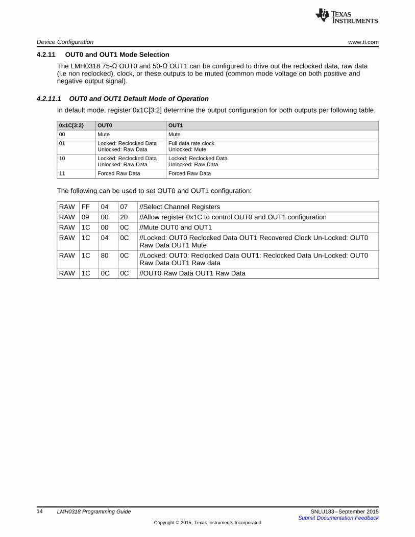
4.2.11 OUT0 and OUT1 Mode SelectionThe LMH0318 75-Ω OUT0 and 50-Ω OUT1 can be configured to drive out the reclocked data, raw data(i.e non reclocked), clock, or these outputs to be muted (common mode voltage on both positive andnegative output signal).
4.2.11.1 OUT0 and OUT1 Default Mode of OperationIn default mode, register 0x1C[3:2] determine the output configuration for both outputs per following table.
0x1C[3:2} OUT0 OUT100 Mute Mute01 Locked: Reclocked Data Full data rate clock
Unlocked: Raw Data Unlocked: Mute10 Locked: Reclocked Data Locked: Reclocked Data
Unlocked: Raw Data Unlocked: Raw Data11 Forced Raw Data Forced Raw Data
The following can be used to set OUT0 and OUT1 configuration:
RAW FF 04 07 //Select Channel RegistersRAW 09 00 20 //Allow register 0x1C to control OUT0 and OUT1 configurationRAW 1C 00 0C //Mute OUT0 and OUT1RAW 1C 04 0C //Locked: OUT0 Reclocked Data OUT1 Recovered Clock Un-Locked: OUT0
Raw Data OUT1 MuteRAW 1C 80 0C //Locked: OUT0: Reclocked Data OUT1: Reclocked Data Un-Locked: OUT0
Raw Data OUT1 Raw dataRAW 1C 0C 0C //OUT0 Raw Data OUT1 Raw Data
14 LMH0318 Programming Guide SNLU183–September 2015Submit Documentation Feedback
Copyright © 2015, Texas Instruments Incorporated
www.ti.com Device Configuration
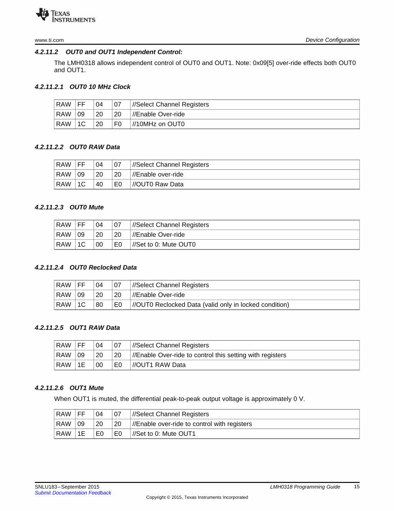
4.2.11.2 OUT0 and OUT1 Independent Control:The LMH0318 allows independent control of OUT0 and OUT1. Note: 0x09[5] over-ride effects both OUT0and OUT1.
4.2.11.2.1 OUT0 10 MHz Clock
RAW FF 04 07 //Select Channel RegistersRAW 09 20 20 //Enable Over-rideRAW 1C 20 F0 //10MHz on OUT0
4.2.11.2.2 OUT0 RAW Data
RAW FF 04 07 //Select Channel RegistersRAW 09 20 20 //Enable over-rideRAW 1C 40 E0 //OUT0 Raw Data
4.2.11.2.3 OUT0 Mute
RAW FF 04 07 //Select Channel RegistersRAW 09 20 20 //Enable Over-rideRAW 1C 00 E0 //Set to 0: Mute OUT0
4.2.11.2.4 OUT0 Reclocked Data
RAW FF 04 07 //Select Channel RegistersRAW 09 20 20 //Enable Over-rideRAW 1C 80 E0 //OUT0 Reclocked Data (valid only in locked condition)
4.2.11.2.5 OUT1 RAW Data
RAW FF 04 07 //Select Channel RegistersRAW 09 20 20 //Enable Over-ride to control this setting with registersRAW 1E 00 E0 //OUT1 RAW Data
4.2.11.2.6 OUT1 MuteWhen OUT1 is muted, the differential peak-to-peak output voltage is approximately 0 V.
RAW FF 04 07 //Select Channel RegistersRAW 09 20 20 //Enable over-ride to control with registersRAW 1E E0 E0 //Set to 0: Mute OUT1
15SNLU183–September 2015 LMH0318 Programming GuideSubmit Documentation Feedback
Copyright © 2015, Texas Instruments Incorporated

Device Configuration www.ti.com
4.2.11.2.7 OUT1 Reclocked Data
RAW FF 04 07 //Select Channel RegistersRAW 09 20 20 //Enable over-rideRAW 1E 20 E0 //Locked: OUT1 Reclocked Data (valid only in locked condition)
4.2.11.2.8 OUT1 Full Rate ClockThe following sequence enables full rate or line recovered clock.
RAW FF 04 07 //Select Channel RegistersRAW 09 20 20 //Enable over-rideRAW 1E 40 E0 //OUT1 full rate clock
4.2.11.2.9 OUT1 10 MHz Clock
RAW FF 04 07 //Select Channel RegistersRAW 09 20 20 //Enable over-rideRAW 1E A0 E0 //Enable 10 MHz on OUT1
4.2.12 Invert OUT1 Data PolarityFor ease of layout, there may be a need to invert the polarity of the OUT1 differential pair.
RAW FF 04 07 //Select Channel RegistersRAW 1E 80 80 //Invert OUT1 Polarity
4.2.13 OUT0 and OUT1 SettingsThe LMH0318 has programmable VOD (Voltage Output Differential), Pre-Emphasis (OUT0), PW (PulseWidth OUT0 settings), De-Emphasis Settings, and individual power-down settings
16 LMH0318 Programming Guide SNLU183–September 2015Submit Documentation Feedback
Copyright © 2015, Texas Instruments Incorporated
www.ti.com Device Configuration
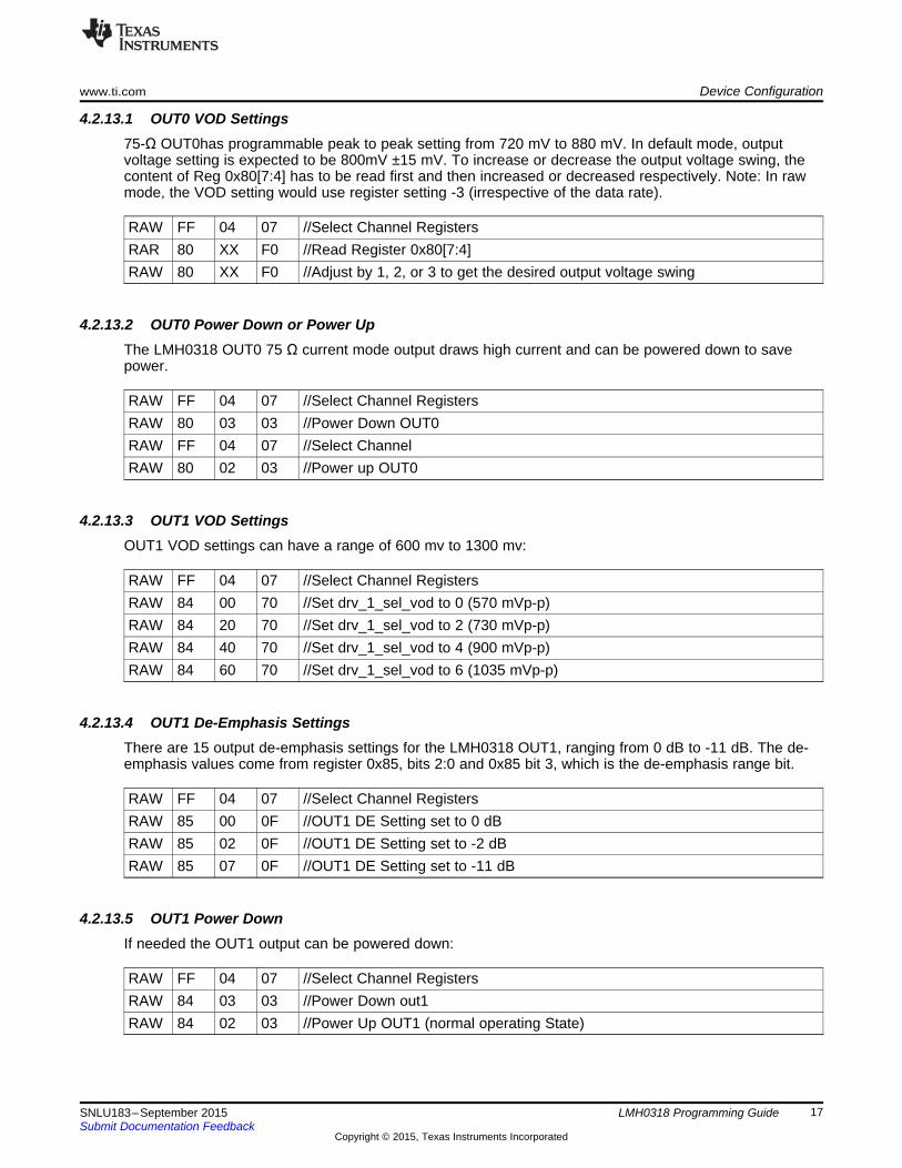
4.2.13.1 OUT0 VOD Settings75-Ω OUT0has programmable peak to peak setting from 720 mV to 880 mV. In default mode, outputvoltage setting is expected to be 800mV ±15 mV. To increase or decrease the output voltage swing, thecontent of Reg 0x80[7:4] has to be read first and then increased or decreased respectively. Note: In rawmode, the VOD setting would use register setting -3 (irrespective of the data rate).
RAW FF 04 07 //Select Channel RegistersRAR 80 XX F0 //Read Register 0x80[7:4]RAW 80 XX F0 //Adjust by 1, 2, or 3 to get the desired output voltage swing
4.2.13.2 OUT0 Power Down or Power UpThe LMH0318 OUT0 75 Ω current mode output draws high current and can be powered down to savepower.
RAW FF 04 07 //Select Channel RegistersRAW 80 03 03 //Power Down OUT0RAW FF 04 07 //Select ChannelRAW 80 02 03 //Power up OUT0
4.2.13.3 OUT1 VOD SettingsOUT1 VOD settings can have a range of 600 mv to 1300 mv:
RAW FF 04 07 //Select Channel RegistersRAW 84 00 70 //Set drv_1_sel_vod to 0 (570 mVp-p)RAW 84 20 70 //Set drv_1_sel_vod to 2 (730 mVp-p)RAW 84 40 70 //Set drv_1_sel_vod to 4 (900 mVp-p)RAW 84 60 70 //Set drv_1_sel_vod to 6 (1035 mVp-p)
4.2.13.4 OUT1 De-Emphasis SettingsThere are 15 output de-emphasis settings for the LMH0318 OUT1, ranging from 0 dB to -11 dB. The de-emphasis values come from register 0x85, bits 2:0 and 0x85 bit 3, which is the de-emphasis range bit.
RAW FF 04 07 //Select Channel RegistersRAW 85 00 0F //OUT1 DE Setting set to 0 dBRAW 85 02 0F //OUT1 DE Setting set to -2 dBRAW 85 07 0F //OUT1 DE Setting set to -11 dB
4.2.13.5 OUT1 Power DownIf needed the OUT1 output can be powered down:
RAW FF 04 07 //Select Channel RegistersRAW 84 03 03 //Power Down out1RAW 84 02 03 //Power Up OUT1 (normal operating State)
17SNLU183–September 2015 LMH0318 Programming GuideSubmit Documentation Feedback
Copyright © 2015, Texas Instruments Incorporated
Device Configuration www.ti.com
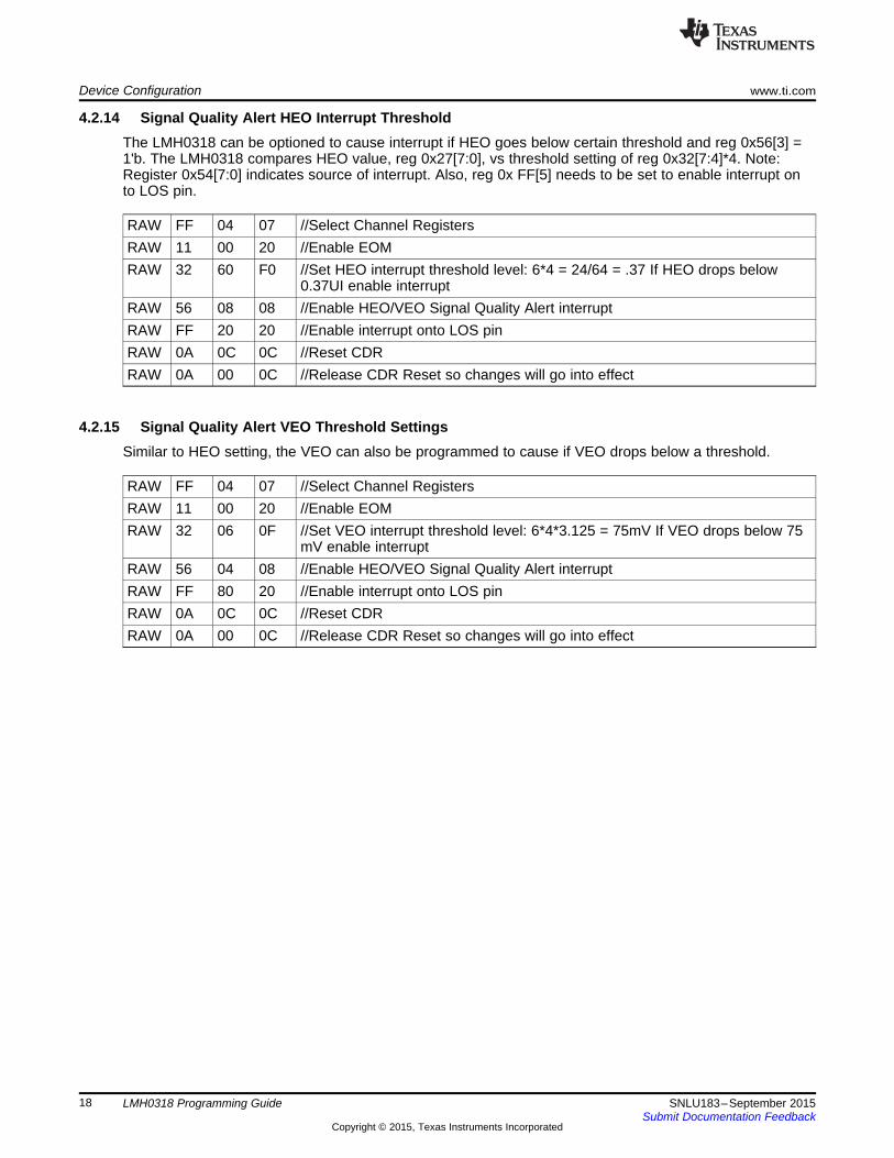
4.2.14 Signal Quality Alert HEO Interrupt ThresholdThe LMH0318 can be optioned to cause interrupt if HEO goes below certain threshold and reg 0x56[3] =1'b. The LMH0318 compares HEO value, reg 0x27[7:0], vs threshold setting of reg 0x32[7:4]*4. Note:Register 0x54[7:0] indicates source of interrupt. Also, reg 0x FF[5] needs to be set to enable interrupt onto LOS pin.
RAW FF 04 07 //Select Channel RegistersRAW 11 00 20 //Enable EOMRAW 32 60 F0 //Set HEO interrupt threshold level: 6*4 = 24/64 = .37 If HEO drops below
0.37UI enable interruptRAW 56 08 08 //Enable HEO/VEO Signal Quality Alert interruptRAW FF 20 20 //Enable interrupt onto LOS pinRAW 0A 0C 0C //Reset CDRRAW 0A 00 0C //Release CDR Reset so changes will go into effect
4.2.15 Signal Quality Alert VEO Threshold SettingsSimilar to HEO setting, the VEO can also be programmed to cause if VEO drops below a threshold.
RAW FF 04 07 //Select Channel RegistersRAW 11 00 20 //Enable EOMRAW 32 06 0F //Set VEO interrupt threshold level: 6*4*3.125 = 75mV If VEO drops below 75
mV enable interruptRAW 56 04 08 //Enable HEO/VEO Signal Quality Alert interruptRAW FF 80 20 //Enable interrupt onto LOS pinRAW 0A 0C 0C //Reset CDRRAW 0A 00 0C //Release CDR Reset so changes will go into effect
18 LMH0318 Programming Guide SNLU183–September 2015Submit Documentation Feedback
Copyright © 2015, Texas Instruments Incorporated
www.ti.com Register Tables
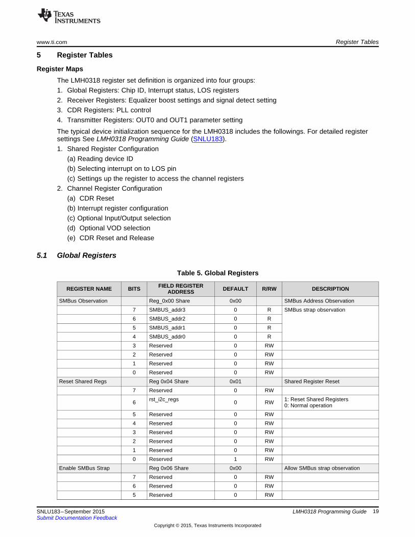
5 Register Tables
Register MapsThe LMH0318 register set definition is organized into four groups:1. Global Registers: Chip ID, Interrupt status, LOS registers2. Receiver Registers: Equalizer boost settings and signal detect setting3. CDR Registers: PLL control4. Transmitter Registers: OUT0 and OUT1 parameter setting
The typical device initialization sequence for the LMH0318 includes the followings. For detailed registersettings See LMH0318 Programming Guide (SNLU183).1. Shared Register Configuration
(a) Reading device ID(b) Selecting interrupt on to LOS pin(c) Settings up the register to access the channel registers
2. Channel Register Configuration(a) CDR Reset(b) Interrupt register configuration(c) Optional Input/Output selection(d) Optional VOD selection(e) CDR Reset and Release
5.1 Global Registers
Table 5. Global Registers
FIELD REGISTERREGISTER NAME BITS DEFAULT R/RW DESCRIPTIONADDRESSSMBus Observation Reg_0x00 Share 0x00 SMBus Address Observation
7 SMBUS_addr3 0 R SMBus strap observation6 SMBUS_addr2 0 R5 SMBUS_addr1 0 R4 SMBUS_addr0 0 R3 Reserved 0 RW2 Reserved 0 RW1 Reserved 0 RW0 Reserved 0 RW
Reset Shared Regs Reg 0x04 Share 0x01 Shared Register Reset7 Reserved 0 RW
rst_i2c_regs 1: Reset Shared Registers6 0 RW 0: Normal operation5 Reserved 0 RW4 Reserved 0 RW3 Reserved 0 RW2 Reserved 0 RW1 Reserved 0 RW0 Reserved 1 RW
Enable SMBus Strap Reg 0x06 Share 0x00 Allow SMBus strap observation7 Reserved 0 RW6 Reserved 0 RW5 Reserved 0 RW
19SNLU183–September 2015 LMH0318 Programming GuideSubmit Documentation Feedback
Copyright © 2015, Texas Instruments Incorporated
Register Tables www.ti.com
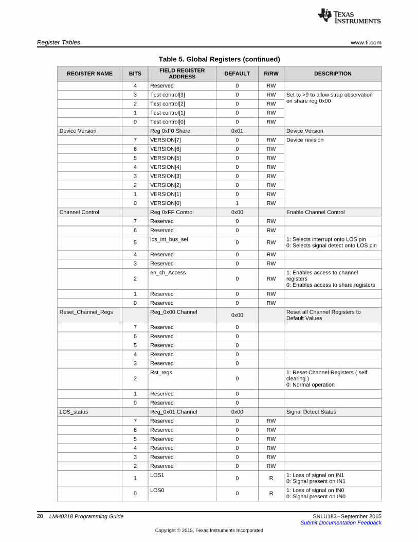
Table 5. Global Registers (continued)FIELD REGISTERREGISTER NAME BITS DEFAULT R/RW DESCRIPTIONADDRESS
4 Reserved 0 RW3 Test control[3] 0 RW Set to >9 to allow strap observation
on share reg 0x002 Test control[2] 0 RW1 Test control[1] 0 RW0 Test control[0] 0 RW
Device Version Reg 0xF0 Share 0x01 Device Version7 VERSION[7] 0 RW Device revision6 VERSION[6] 0 RW5 VERSION[5] 0 RW4 VERSION[4] 0 RW3 VERSION[3] 0 RW2 VERSION[2] 0 RW1 VERSION[1] 0 RW0 VERSION[0] 1 RW
Channel Control Reg 0xFF Control 0x00 Enable Channel Control7 Reserved 0 RW6 Reserved 0 RW
los_int_bus_sel 1: Selects interrupt onto LOS pin5 0 RW 0: Selects signal detect onto LOS pin4 Reserved 0 RW3 Reserved 0 RW
en_ch_Access 1: Enables access to channel2 0 RW registers
0: Enables access to share registers1 Reserved 0 RW0 Reserved 0 RW
Reset_Channel_Regs Reg_0x00 Channel Reset all Channel Registers to0x00 Default Values7 Reserved 06 Reserved 05 Reserved 04 Reserved 03 Reserved 0
Rst_regs 1: Reset Channel Registers ( self2 0 clearing )
0: Normal operation1 Reserved 00 Reserved 0
LOS_status Reg_0x01 Channel 0x00 Signal Detect Status7 Reserved 0 RW6 Reserved 0 RW5 Reserved 0 RW4 Reserved 0 RW3 Reserved 0 RW2 Reserved 0 RW
LOS1 1: Loss of signal on IN11 0 R 0: Signal present on IN1LOS0 1: Loss of signal on IN00 0 R 0: Signal present on IN0
20 LMH0318 Programming Guide SNLU183–September 2015Submit Documentation Feedback
Copyright © 2015, Texas Instruments Incorporated
www.ti.com Register Tables
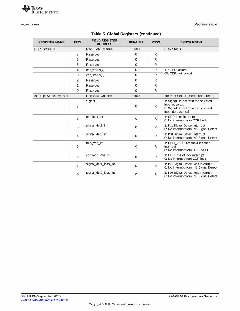
Table 5. Global Registers (continued)FIELD REGISTERREGISTER NAME BITS DEFAULT R/RW DESCRIPTIONADDRESS
CDR_Status_1 Reg_0x02 Channel 0x00 CDR Status7 Reserved 0 R6 Reserved 0 R5 Reserved 0 R4 cdr_status[4] 0 R 11: CDR locked
00: CDR not locked3 cdr_status[3] 0 R2 Reserved 0 R1 Reserved 0 R0 Reserved 0 R
Interrupt Status Register Reg 0x54 Channel 0x00 Interrupt Status ( clears upon read )Sigdet 1: Signal Detect from the selected
input asserted7 0 R 0: Signal Detect from the selectedinput de-asserted
cdr_lock_int 1: CDR Lock interrupt6 0 R 0: No interrupt from CDR Locksignal_det1_int 1: IN1 Signal Detect interrupt5 0 R 0: No interrupt from IN1 Signal Detectsignal_det0_int 1: IN0 Signal Detect interrupt4 0 R 0: No interrupt from IN0 Signal Detectheo_veo_int 1: HEO_VEO Threshold reached
3 0 R interrupt0: No interrupt from HEO_VEO
cdr_lock_loss_int 1: CDR loss of lock interrupt2 0 R 0: No interrupt from CDR locksignal_det1_loss_int 1: IN1 Signal Detect loss interrupt1 0 R 0: No interrupt from IN1 Signal Detectsignal_det0_loss_int 1: IN0 Signal Detect loss interrupt0 0 R 0: No interrupt from IN0 Signal Detect
21SNLU183–September 2015 LMH0318 Programming GuideSubmit Documentation Feedback
Copyright © 2015, Texas Instruments Incorporated

Register Tables www.ti.com
Table 5. Global Registers (continued)FIELD REGISTERREGISTER NAME BITS DEFAULT R/RW DESCRIPTIONADDRESS
Interrupt Control Reg 0x56 Channel 0x00 Interrupt Mask7 Reserved 0 RW
cdr_lock_int_en 1: Enable Interrupt if CDR lock isachieved6 0 RW 0: Disable interrupt if CDR lock isachieved
signal_det1_int_en 1: Enable interrupt if IN1 SignalDetect is asserted5 0 RW 0: Disable interrupt if IN1 SignalDetect is asserted
signal_det0_int_en 1: Enable interrupt if IN0 SignalDetect is asserted4 0 RW 0: Disable interrupt if IN0 SignalDetect is asserted
heo_veo_int_en 1: Enable interrupt if HEO-VEOthreshold is reached3 0 RW 0: Disable interrupt due to HEO-VEOthreshold
cdr_lock_loss_int_en 1: Enable interrupt if CDR loses lock2 0 RW 0: Disable interrupt if CDR loses locksignal_det1_loss_int_en 1: Enable interrupt if there is loss of
signal on IN11 0 RW 0: Disable interrupt if there is loss ofsignal on IN1
signal_det0_loss_int_en 1: Enable interrupt if there is loss ofsignal on IN00 0 RW 0: Disable interrupt if there is loss ofsignal on IN0
22 LMH0318 Programming Guide SNLU183–September 2015Submit Documentation Feedback
Copyright © 2015, Texas Instruments Incorporated
www.ti.com Register Tables
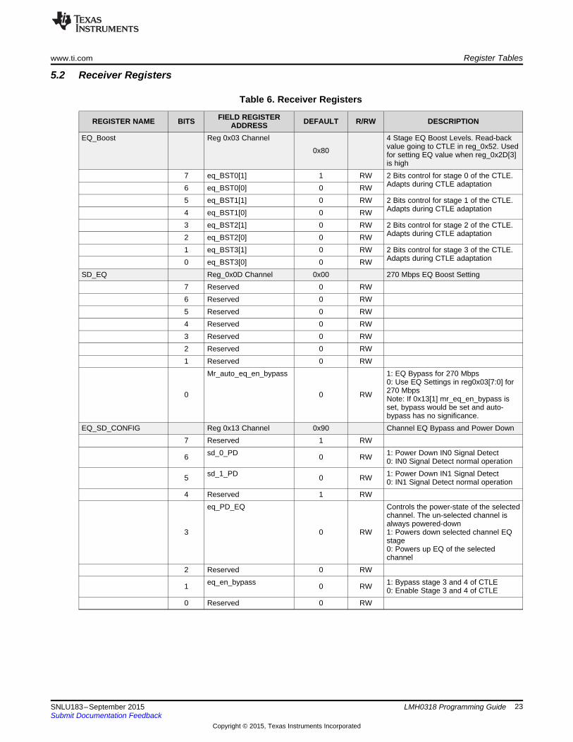
5.2 Receiver Registers
Table 6. Receiver Registers
FIELD REGISTERREGISTER NAME BITS DEFAULT R/RW DESCRIPTIONADDRESSEQ_Boost Reg 0x03 Channel 4 Stage EQ Boost Levels. Read-back
value going to CTLE in reg_0x52. Used0x80 for setting EQ value when reg_0x2D[3]is high
7 eq_BST0[1] 1 RW 2 Bits control for stage 0 of the CTLE.Adapts during CTLE adaptation6 eq_BST0[0] 0 RW
5 eq_BST1[1] 0 RW 2 Bits control for stage 1 of the CTLE.Adapts during CTLE adaptation4 eq_BST1[0] 0 RW
3 eq_BST2[1] 0 RW 2 Bits control for stage 2 of the CTLE.Adapts during CTLE adaptation2 eq_BST2[0] 0 RW
1 eq_BST3[1] 0 RW 2 Bits control for stage 3 of the CTLE.Adapts during CTLE adaptation0 eq_BST3[0] 0 RW
SD_EQ Reg_0x0D Channel 0x00 270 Mbps EQ Boost Setting7 Reserved 0 RW6 Reserved 0 RW5 Reserved 0 RW4 Reserved 0 RW3 Reserved 0 RW2 Reserved 0 RW1 Reserved 0 RW
Mr_auto_eq_en_bypass 1: EQ Bypass for 270 Mbps0: Use EQ Settings in reg0x03[7:0] for270 Mbps0 0 RW Note: If 0x13[1] mr_eq_en_bypass isset, bypass would be set and auto-bypass has no significance.
EQ_SD_CONFIG Reg 0x13 Channel 0x90 Channel EQ Bypass and Power Down7 Reserved 1 RW
sd_0_PD 1: Power Down IN0 Signal Detect6 0 RW 0: IN0 Signal Detect normal operationsd_1_PD 1: Power Down IN1 Signal Detect5 0 RW 0: IN1 Signal Detect normal operation
4 Reserved 1 RWeq_PD_EQ Controls the power-state of the selected
channel. The un-selected channel isalways powered-down
3 0 RW 1: Powers down selected channel EQstage0: Powers up EQ of the selectedchannel
2 Reserved 0 RWeq_en_bypass 1: Bypass stage 3 and 4 of CTLE1 0 RW 0: Enable Stage 3 and 4 of CTLE
0 Reserved 0 RW
23SNLU183–September 2015 LMH0318 Programming GuideSubmit Documentation Feedback
Copyright © 2015, Texas Instruments Incorporated
Register Tables www.ti.com
Table 6. Receiver Registers (continued)FIELD REGISTERREGISTER NAME BITS DEFAULT R/RW DESCRIPTIONADDRESS
SD0_CONFIG Reg 0x14 Channel 0x00 IN0 Signal Detect Threshold Setting7 Reserved 0 RW6 Reserved 0 RW5 sd_0_refa_sel[1] 0 RW Controls signal detect SDH- Assert [5:4],
SDL- De-Assert [3:2], thresholds for IN04 sd_0_refa_sel[0] 0 RW 0000: Default levels (nominal)3 sd_0_refd_sel[1] 0 RW 0101: Nominal -2 mV
1010: Nominal +5 mVsd_0_refd_sel[0]2 0 RW 1111: Nominal +3 mV1 Reserved 0 RW0 Reserved 0 RW
SD1_CONFIG Reg_0x15 Channel 0x00 IN1 Signal Detect Threshold Setting7 Reserved 0 RW6 Reserved 0 RW5 sd_1_refa_sel[1] 0 RW Controls signal detect SDH- Assert [5:4],
SDL- De-Assert [3:2], thresholds for IN14 sd_1_refa_sel[0] 0 RW 0000: Default levels (nominal)3 sd_1_refd_sel[1] 0 RW 0101: Nominal -2 mV
1010: Nominal +5 mVsd_1_refd_sel[0]2 0 RW 1111: Nominal +3 mV1 Reserved 0 RW0 Reserved 0 RW
EQ_BOOST_OV Reg_0x2D Channel 0x88 EQ Boost Override7 Reserved 1 RW6 Reserved 0 RW5 Reserved 0 RW4 Reserved 0 RW
reg_eq_bst_ov 1: Enable EQ boost over ride SeeLMH0318 Programming Guide3 1 RW (SNLU183)0: Disable EQ boost over ride
2 Reserved 0 RW1 Reserved 0 RW0 Reserved 0 RW
CTLE Setting Reg_0x31 Channel CTLE Mode of Operation and0x00 Input/Output Mux Selection7 Reserved 0 RW6 adapt_mode[1] 00: Normal Operation - Manual CTLE
Settingadapt_mode[0] 01: Test Mode - See the LMH031800 RW Programming Guide (SNLU183) for5detailsOther Settings - Invalid
4 Reserved 0 RW3 Reserved 0 RW2 Reserved 0 RW1 input_mux_ch_sel[1] 0 RW IN0/1 and OUT0/1 selection
00: selects IN0 and OUT0/1input_mux_ch_sel[0] 01: selects IN0 and OUT00 0 RW 10: selects IN1 and OUT1
11: selects IN1 and OUT0/1
24 LMH0318 Programming Guide SNLU183–September 2015Submit Documentation Feedback
Copyright © 2015, Texas Instruments Incorporated

www.ti.com Register Tables
Table 6. Receiver Registers (continued)FIELD REGISTERREGISTER NAME BITS DEFAULT R/RW DESCRIPTIONADDRESS
LOW_RATE_ Reg 0x3A Channel HD and SD EQ Level0x00EQ_BST7 fixed_eq_BST0[1] 0 RW When CTLE is operating in test mode,
Reg 0x3A[7:0] forces fixed EQ setting.6 fixed_eq_BST0[0] 0 RW In normal operating manual mode5 fixed_eq_BST1[1] 0 RW Reg_0x03 forces EQ boost. See
LMH0318 Programming Guide4 fixed_eq_BST1[0] 0 RW(SNLU183) for details
3 fixed_eq_BST2[1] 0 RW2 fixed_eq_BST2[0] 0 RW1 fixed_eq_BST3[1] 0 RW0 fixed_eq_BST3[0] 0 RW
BST_Indx0 Reg_0x40 Channel Index0 4 Stage EQ Boost. See0x00 LMH0318 Programming Guide
(SNLU183)7 I0_BST0[1] 0 RW Index 0 Boost Stage 0 bit 16 I0_BST0[0] 0 RW Index 0 Boost Stage 0 bit 05 I0_BST1[1] 0 RW Index 0 Boost Stage 1 bit 14 I0_BST1[0] 0 RW Index 0 Boost Stage 1 bit 03 I0_BST2[1] 0 RW Index 0 Boost Stage 2 bit 12 I0_BST2[0] 0 RW Index 0 Boost Stage 2 bit 01 I0_BST3[1] 0 RW Index 0 Boost Stage 3 bit 10 I0_BST3[0] 0 RW Index 0 Boost Stage 3 bit 0
BST_Indx1 Reg 0x41 Channel 0x40 Index1 4 Stage EQ Boost.7 I1_BST0[1] 0 RW Index 1 Boost Stage 0 bit 16 I1_BST0[0] 1 RW Index 1 Boost Stage 0 bit 05 I1_BST1[1] 0 RW Index 1 Boost Stage 1 bit 14 I1_BST1[0] 0 RW Index 1 Boost Stage 1 bit 03 I1_BST2[1] 0 RW Index 1 Boost Stage 2 bit 12 I1_BST2[0] 0 RW Index 1 Boost Stage 2 bit 01 I1_BST3[1] 0 RW Index 1 Boost Stage 3 bit 10 I1_BST3[0] 0 RW Index 1 Boost Stage 3 bit 0
BST_Indx2 Reg 0x42 Channel 0x80 Index2 4 Stage EQ Boost.7 I2_BST0[1] 1 RW Index 2 Boost Stage 0 bit 16 I2_BST0[0] 0 RW Index 2 Boost Stage 0 bit 05 I2_BST1[1] 0 RW Index 2 Boost Stage 1 bit 14 I2_BST1[0] 0 RW Index 2 Boost Stage 1 bit 03 I2_BST2[1] 0 RW Index 2 Boost Stage 2 bit 12 I2_BST2[0] 0 RW Index 2 Boost Stage 2 bit 01 I2_BST3[1] 0 RW Index 2 Boost Stage 3 bit 10 I2_BST3[0] 0 RW Index 2 Boost Stage 3 bit 0
25SNLU183–September 2015 LMH0318 Programming GuideSubmit Documentation Feedback
Copyright © 2015, Texas Instruments Incorporated
Register Tables www.ti.com
Table 6. Receiver Registers (continued)FIELD REGISTERREGISTER NAME BITS DEFAULT R/RW DESCRIPTIONADDRESS
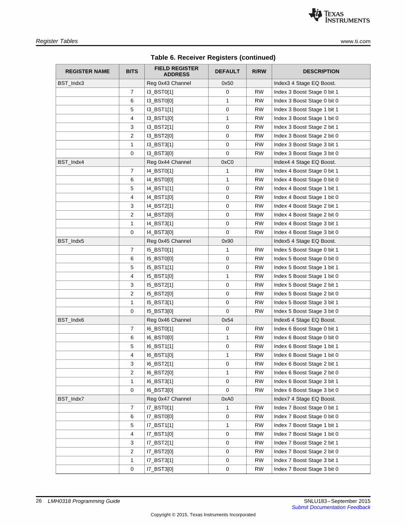
BST_Indx3 Reg 0x43 Channel 0x50 Index3 4 Stage EQ Boost.7 I3_BST0[1] 0 RW Index 3 Boost Stage 0 bit 16 I3_BST0[0] 1 RW Index 3 Boost Stage 0 bit 05 I3_BST1[1] 0 RW Index 3 Boost Stage 1 bit 14 I3_BST1[0] 1 RW Index 3 Boost Stage 1 bit 03 I3_BST2[1] 0 RW Index 3 Boost Stage 2 bit 12 I3_BST2[0] 0 RW Index 3 Boost Stage 2 bit 01 I3_BST3[1] 0 RW Index 3 Boost Stage 3 bit 10 I3_BST3[0] 0 RW Index 3 Boost Stage 3 bit 0
BST_Indx4 Reg 0x44 Channel 0xC0 Index4 4 Stage EQ Boost.7 I4_BST0[1] 1 RW Index 4 Boost Stage 0 bit 16 I4_BST0[0] 1 RW Index 4 Boost Stage 0 bit 05 I4_BST1[1] 0 RW Index 4 Boost Stage 1 bit 14 I4_BST1[0] 0 RW Index 4 Boost Stage 1 bit 03 I4_BST2[1] 0 RW Index 4 Boost Stage 2 bit 12 I4_BST2[0] 0 RW Index 4 Boost Stage 2 bit 01 I4_BST3[1] 0 RW Index 4 Boost Stage 3 bit 10 I4_BST3[0] 0 RW Index 4 Boost Stage 3 bit 0
BST_Indx5 Reg 0x45 Channel 0x90 Index5 4 Stage EQ Boost.7 I5_BST0[1] 1 RW Index 5 Boost Stage 0 bit 16 I5_BST0[0] 0 RW Index 5 Boost Stage 0 bit 05 I5_BST1[1] 0 RW Index 5 Boost Stage 1 bit 14 I5_BST1[0] 1 RW Index 5 Boost Stage 1 bit 03 I5_BST2[1] 0 RW Index 5 Boost Stage 2 bit 12 I5_BST2[0] 0 RW Index 5 Boost Stage 2 bit 01 I5_BST3[1] 0 RW Index 5 Boost Stage 3 bit 10 I5_BST3[0] 0 RW Index 5 Boost Stage 3 bit 0
BST_Indx6 Reg 0x46 Channel 0x54 Index6 4 Stage EQ Boost.7 I6_BST0[1] 0 RW Index 6 Boost Stage 0 bit 16 I6_BST0[0] 1 RW Index 6 Boost Stage 0 bit 05 I6_BST1[1] 0 RW Index 6 Boost Stage 1 bit 14 I6_BST1[0] 1 RW Index 6 Boost Stage 1 bit 03 I6_BST2[1] 0 RW Index 6 Boost Stage 2 bit 12 I6_BST2[0] 1 RW Index 6 Boost Stage 2 bit 01 I6_BST3[1] 0 RW Index 6 Boost Stage 3 bit 10 I6_BST3[0] 0 RW Index 6 Boost Stage 3 bit 0
BST_Indx7 Reg 0x47 Channel 0xA0 Index7 4 Stage EQ Boost.7 I7_BST0[1] 1 RW Index 7 Boost Stage 0 bit 16 I7_BST0[0] 0 RW Index 7 Boost Stage 0 bit 05 I7_BST1[1] 1 RW Index 7 Boost Stage 1 bit 14 I7_BST1[0] 0 RW Index 7 Boost Stage 1 bit 03 I7_BST2[1] 0 RW Index 7 Boost Stage 2 bit 12 I7_BST2[0] 0 RW Index 7 Boost Stage 2 bit 01 I7_BST3[1] 0 RW Index 7 Boost Stage 3 bit 10 I7_BST3[0] 0 RW Index 7 Boost Stage 3 bit 0
26 LMH0318 Programming Guide SNLU183–September 2015Submit Documentation Feedback
Copyright © 2015, Texas Instruments Incorporated

www.ti.com Register Tables
Table 6. Receiver Registers (continued)FIELD REGISTERREGISTER NAME BITS DEFAULT R/RW DESCRIPTIONADDRESS
BST_Indx8 Reg 0x48 Channel 0xB0 Index8 4 Stage EQ Boost.7 I8_BST0[1] 1 RW Index 8 Boost Stage 0 bit 16 I8_BST0[0] 0 RW Index 8 Boost Stage 0 bit 05 I8_BST1[1] 1 RW Index 8 Boost Stage 1 bit 14 I8_BST1[0] 1 RW Index 8 Boost Stage 1 bit 03 I8_BST2[1] 0 RW Index 8 Boost Stage 2 bit 12 I8_BST2[0] 0 RW Index 8 Boost Stage 2 bit 01 I8_BST3[1] 0 RW Index 8 Boost Stage 3 bit 10 I8_BST3[0] 0 RW Index 8 Boost Stage 3 bit 0
BST_Indx9 Reg 0x49 Channel 0X95 0x95 Index9 4 Stage EQ Boost.7 I9_BST0[1] 1 RW Index 9 Boost Stage 0 bit 16 I9_BST0[0] 0 RW Index 9 Boost Stage 0 bit 05 I9_BST1[1] 0 RW Index 9 Boost Stage 1 bit 14 I9_BST1[0] 1 RW Index 9 Boost Stage 1 bit 03 I9_BST2[1] 0 RW Index 9 Boost Stage 2 bit 12 I9_BST2[0] 1 RW Index 9 Boost Stage 2 bit 01 I9_BST3[1] 0 RW Index 9 Boost Stage 3 bit 10 I9_BST3[0] 1 RW Index 9 Boost Stage 3 bit 0
BST_Indx10 Reg 0x4A Channel 0x69 Index10 4 Stage EQ Boost.7 I10_BST0[1] 0 RW Index 10 Boost Stage 0 bit 16 I10_BST0[0] 1 RW Index 10 Boost Stage 0 bit 05 I10_BST1[1] 1 RW Index 10 Boost Stage 1 bit 14 I10_BST1[0] 0 RW Index 10 Boost Stage 1 bit 03 I10_BST2[1] 1 RW Index 10 Boost Stage 2 bit 12 I10_BST2[0] 0 RW Index 10 Boost Stage 2 bit 01 I10_BST3[1] 0 RW Index 10 Boost Stage 3 bit 10 I10_BST3[0] 1 RW Index 10 Boost Stage 3 bit 0
BST_Indx11 Reg 0x4B Channel 0xD5 Index11 4 Stage EQ Boost.7 I11_BST0[1] 1 RW Index 11 Boost Stage 0 bit 16 I11_BST0[0] 1 RW Index 11 Boost Stage 0 bit 05 I11_BST1[1] 0 RW Index 11 Boost Stage 1 bit 14 I11_BST1[0] 1 RW Index 11 Boost Stage 1 bit 03 I11_BST2[1] 0 RW Index 11 Boost Stage 2 bit 12 I11_BST2[0] 1 RW Index 11 Boost Stage 2 bit 01 I11_BST3[1] 0 RW Index 11 Boost Stage 3 bit 10 I11_BST3[0] 1 RW Index 11 Boost Stage 3 bit 0
BSTIndx12 Reg 0x4C Channel 0x99 Index12 4 Stage EQ Boost.7 I12_BST0[1] 1 RW Index 12 Boost Stage 0 bit 16 I12_BST0[0] 0 RW Index 12 Boost Stage 0 bit 05 I12_BST1[1] 0 RW Index 12 Boost Stage 1 bit 14 I12_BST1[0] 1 RW Index 12 Boost Stage 1 bit 03 I12_BST2[1] 1 RW Index 12 Boost Stage 2 bit 12 I12_BST2[0] 0 RW Index 12 Boost Stage 2 bit 01 I12_BST3[1] 0 RW Index 12 Boost Stage 3 bit 10 I12_BST3[0] 1 RW Index 12 Boost Stage 3 bit 0
27SNLU183–September 2015 LMH0318 Programming GuideSubmit Documentation Feedback
Copyright © 2015, Texas Instruments Incorporated
Register Tables www.ti.com
Table 6. Receiver Registers (continued)FIELD REGISTERREGISTER NAME BITS DEFAULT R/RW DESCRIPTIONADDRESS
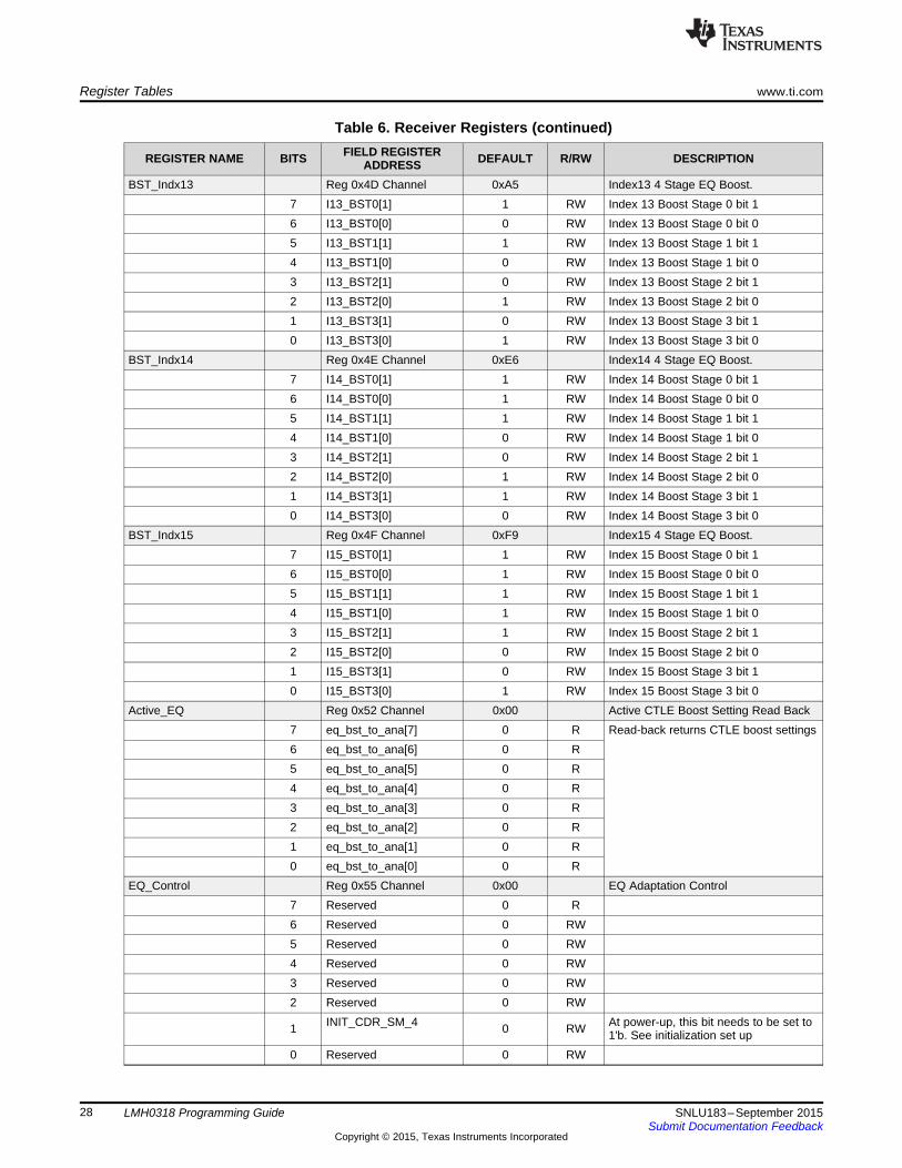
BST_Indx13 Reg 0x4D Channel 0xA5 Index13 4 Stage EQ Boost.7 I13_BST0[1] 1 RW Index 13 Boost Stage 0 bit 16 I13_BST0[0] 0 RW Index 13 Boost Stage 0 bit 05 I13_BST1[1] 1 RW Index 13 Boost Stage 1 bit 14 I13_BST1[0] 0 RW Index 13 Boost Stage 1 bit 03 I13_BST2[1] 0 RW Index 13 Boost Stage 2 bit 12 I13_BST2[0] 1 RW Index 13 Boost Stage 2 bit 01 I13_BST3[1] 0 RW Index 13 Boost Stage 3 bit 10 I13_BST3[0] 1 RW Index 13 Boost Stage 3 bit 0
BST_Indx14 Reg 0x4E Channel 0xE6 Index14 4 Stage EQ Boost.7 I14_BST0[1] 1 RW Index 14 Boost Stage 0 bit 16 I14_BST0[0] 1 RW Index 14 Boost Stage 0 bit 05 I14_BST1[1] 1 RW Index 14 Boost Stage 1 bit 14 I14_BST1[0] 0 RW Index 14 Boost Stage 1 bit 03 I14_BST2[1] 0 RW Index 14 Boost Stage 2 bit 12 I14_BST2[0] 1 RW Index 14 Boost Stage 2 bit 01 I14_BST3[1] 1 RW Index 14 Boost Stage 3 bit 10 I14_BST3[0] 0 RW Index 14 Boost Stage 3 bit 0
BST_Indx15 Reg 0x4F Channel 0xF9 Index15 4 Stage EQ Boost.7 I15_BST0[1] 1 RW Index 15 Boost Stage 0 bit 16 I15_BST0[0] 1 RW Index 15 Boost Stage 0 bit 05 I15_BST1[1] 1 RW Index 15 Boost Stage 1 bit 14 I15_BST1[0] 1 RW Index 15 Boost Stage 1 bit 03 I15_BST2[1] 1 RW Index 15 Boost Stage 2 bit 12 I15_BST2[0] 0 RW Index 15 Boost Stage 2 bit 01 I15_BST3[1] 0 RW Index 15 Boost Stage 3 bit 10 I15_BST3[0] 1 RW Index 15 Boost Stage 3 bit 0
Active_EQ Reg 0x52 Channel 0x00 Active CTLE Boost Setting Read Back7 eq_bst_to_ana[7] 0 R Read-back returns CTLE boost settings6 eq_bst_to_ana[6] 0 R5 eq_bst_to_ana[5] 0 R4 eq_bst_to_ana[4] 0 R3 eq_bst_to_ana[3] 0 R2 eq_bst_to_ana[2] 0 R1 eq_bst_to_ana[1] 0 R0 eq_bst_to_ana[0] 0 R
EQ_Control Reg 0x55 Channel 0x00 EQ Adaptation Control7 Reserved 0 R6 Reserved 0 RW5 Reserved 0 RW4 Reserved 0 RW3 Reserved 0 RW2 Reserved 0 RW
INIT_CDR_SM_4 At power-up, this bit needs to be set to1 0 RW 1'b. See initialization set up0 Reserved 0 RW
28 LMH0318 Programming Guide SNLU183–September 2015Submit Documentation Feedback
Copyright © 2015, Texas Instruments Incorporated
www.ti.com Register Tables
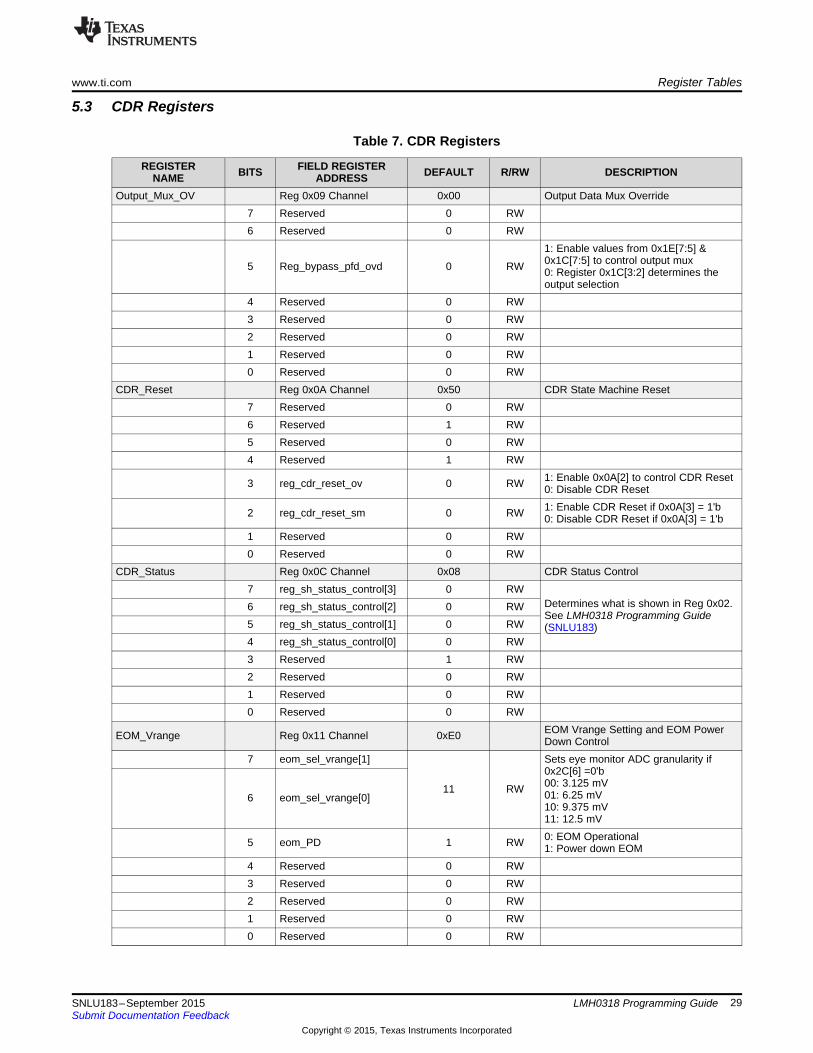
5.3 CDR Registers
Table 7. CDR Registers
REGISTER FIELD REGISTERBITS DEFAULT R/RW DESCRIPTIONNAME ADDRESSOutput_Mux_OV Reg 0x09 Channel 0x00 Output Data Mux Override
7 Reserved 0 RW6 Reserved 0 RW
1: Enable values from 0x1E[7:5] &0x1C[7:5] to control output mux5 Reg_bypass_pfd_ovd 0 RW 0: Register 0x1C[3:2] determines theoutput selection
4 Reserved 0 RW3 Reserved 0 RW2 Reserved 0 RW1 Reserved 0 RW0 Reserved 0 RW
CDR_Reset Reg 0x0A Channel 0x50 CDR State Machine Reset7 Reserved 0 RW6 Reserved 1 RW5 Reserved 0 RW4 Reserved 1 RW
1: Enable 0x0A[2] to control CDR Reset3 reg_cdr_reset_ov 0 RW 0: Disable CDR Reset1: Enable CDR Reset if 0x0A[3] = 1'b2 reg_cdr_reset_sm 0 RW 0: Disable CDR Reset if 0x0A[3] = 1'b
1 Reserved 0 RW0 Reserved 0 RW
CDR_Status Reg 0x0C Channel 0x08 CDR Status Control7 reg_sh_status_control[3] 0 RW
Determines what is shown in Reg 0x02.6 reg_sh_status_control[2] 0 RWSee LMH0318 Programming Guide
5 reg_sh_status_control[1] 0 RW (SNLU183)4 reg_sh_status_control[0] 0 RW3 Reserved 1 RW2 Reserved 0 RW1 Reserved 0 RW0 Reserved 0 RW
EOM Vrange Setting and EOM PowerEOM_Vrange Reg 0x11 Channel 0xE0 Down Control7 eom_sel_vrange[1] Sets eye monitor ADC granularity if
0x2C[6] =0'b00: 3.125 mV11 RW 01: 6.25 mV6 eom_sel_vrange[0]10: 9.375 mV11: 12.5 mV0: EOM Operational5 eom_PD 1 RW 1: Power down EOM
4 Reserved 0 RW3 Reserved 0 RW2 Reserved 0 RW1 Reserved 0 RW0 Reserved 0 RW
29SNLU183–September 2015 LMH0318 Programming GuideSubmit Documentation Feedback
Copyright © 2015, Texas Instruments Incorporated
Register Tables www.ti.com
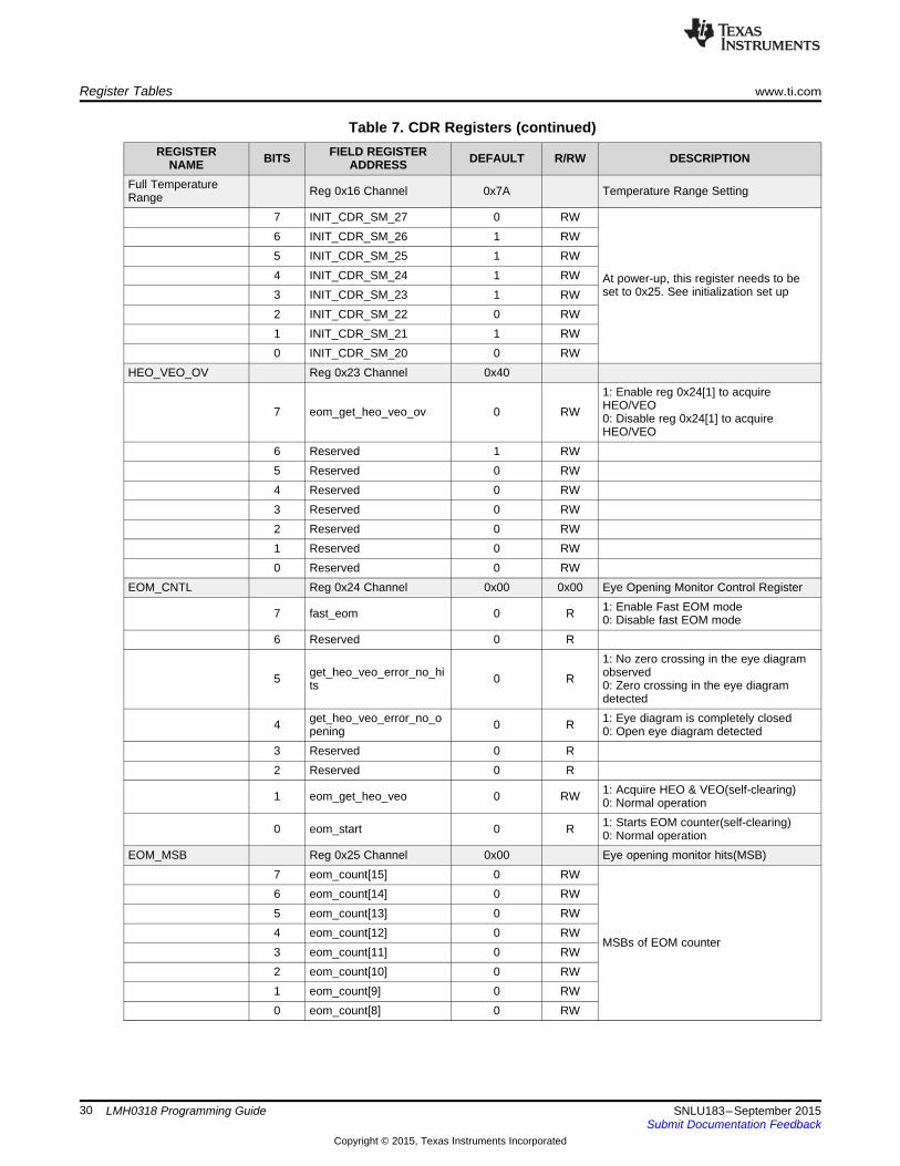
Table 7. CDR Registers (continued)REGISTER FIELD REGISTERBITS DEFAULT R/RW DESCRIPTIONNAME ADDRESS
Full Temperature Reg 0x16 Channel 0x7A Temperature Range SettingRange7 INIT_CDR_SM_27 0 RW6 INIT_CDR_SM_26 1 RW5 INIT_CDR_SM_25 1 RW4 INIT_CDR_SM_24 1 RW At power-up, this register needs to be
set to 0x25. See initialization set up3 INIT_CDR_SM_23 1 RW2 INIT_CDR_SM_22 0 RW1 INIT_CDR_SM_21 1 RW0 INIT_CDR_SM_20 0 RW
HEO_VEO_OV Reg 0x23 Channel 0x401: Enable reg 0x24[1] to acquireHEO/VEO7 eom_get_heo_veo_ov 0 RW 0: Disable reg 0x24[1] to acquireHEO/VEO
6 Reserved 1 RW5 Reserved 0 RW4 Reserved 0 RW3 Reserved 0 RW2 Reserved 0 RW1 Reserved 0 RW0 Reserved 0 RW
EOM_CNTL Reg 0x24 Channel 0x00 0x00 Eye Opening Monitor Control Register1: Enable Fast EOM mode7 fast_eom 0 R 0: Disable fast EOM mode
6 Reserved 0 R1: No zero crossing in the eye diagram
get_heo_veo_error_no_hi observed5 0 Rts 0: Zero crossing in the eye diagramdetected
get_heo_veo_error_no_o 1: Eye diagram is completely closed4 0 Rpening 0: Open eye diagram detected3 Reserved 0 R2 Reserved 0 R
1: Acquire HEO & VEO(self-clearing)1 eom_get_heo_veo 0 RW 0: Normal operation1: Starts EOM counter(self-clearing)0 eom_start 0 R 0: Normal operation
EOM_MSB Reg 0x25 Channel 0x00 Eye opening monitor hits(MSB)7 eom_count[15] 0 RW6 eom_count[14] 0 RW5 eom_count[13] 0 RW4 eom_count[12] 0 RW
MSBs of EOM counter3 eom_count[11] 0 RW2 eom_count[10] 0 RW1 eom_count[9] 0 RW0 eom_count[8] 0 RW
30 LMH0318 Programming Guide SNLU183–September 2015Submit Documentation Feedback
Copyright © 2015, Texas Instruments Incorporated
www.ti.com Register Tables
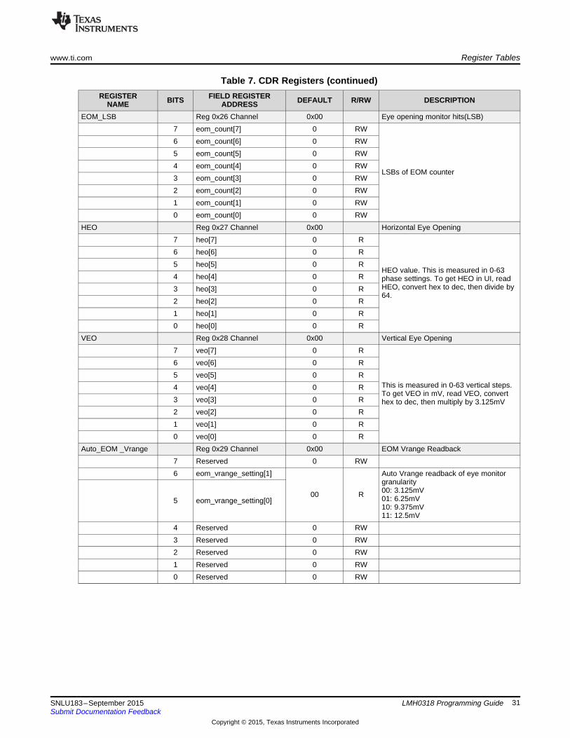
Table 7. CDR Registers (continued)REGISTER FIELD REGISTERBITS DEFAULT R/RW DESCRIPTIONNAME ADDRESS
EOM_LSB Reg 0x26 Channel 0x00 Eye opening monitor hits(LSB)7 eom_count[7] 0 RW6 eom_count[6] 0 RW5 eom_count[5] 0 RW4 eom_count[4] 0 RW
LSBs of EOM counter3 eom_count[3] 0 RW2 eom_count[2] 0 RW1 eom_count[1] 0 RW0 eom_count[0] 0 RW
HEO Reg 0x27 Channel 0x00 Horizontal Eye Opening7 heo[7] 0 R6 heo[6] 0 R5 heo[5] 0 R
HEO value. This is measured in 0-634 heo[4] 0 R phase settings. To get HEO in UI, read
HEO, convert hex to dec, then divide by3 heo[3] 0 R64.
2 heo[2] 0 R1 heo[1] 0 R0 heo[0] 0 R
VEO Reg 0x28 Channel 0x00 Vertical Eye Opening7 veo[7] 0 R6 veo[6] 0 R5 veo[5] 0 R
This is measured in 0-63 vertical steps.4 veo[4] 0 RTo get VEO in mV, read VEO, convert
3 veo[3] 0 R hex to dec, then multiply by 3.125mV2 veo[2] 0 R1 veo[1] 0 R0 veo[0] 0 R
Auto_EOM _Vrange Reg 0x29 Channel 0x00 EOM Vrange Readback7 Reserved 0 RW6 eom_vrange_setting[1] Auto Vrange readback of eye monitor
granularity00: 3.125mV00 R 01: 6.25mV5 eom_vrange_setting[0]10: 9.375mV11: 12.5mV
4 Reserved 0 RW3 Reserved 0 RW2 Reserved 0 RW1 Reserved 0 RW0 Reserved 0 RW
31SNLU183–September 2015 LMH0318 Programming GuideSubmit Documentation Feedback
Copyright © 2015, Texas Instruments Incorporated
Register Tables www.ti.com
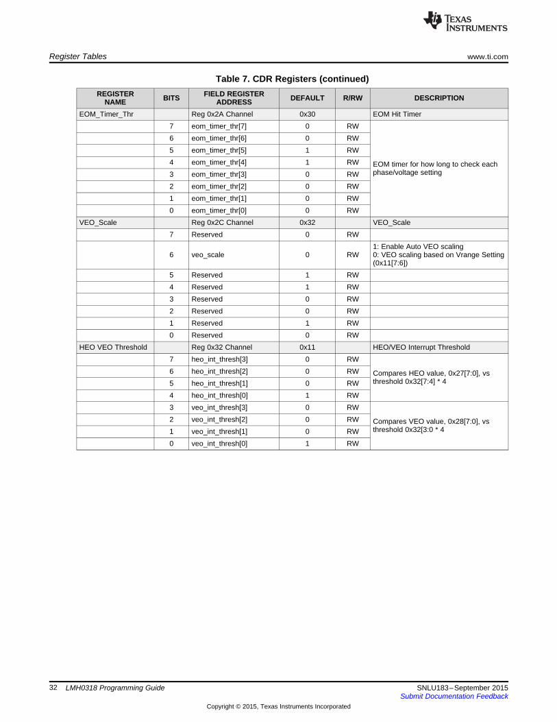
Table 7. CDR Registers (continued)REGISTER FIELD REGISTERBITS DEFAULT R/RW DESCRIPTIONNAME ADDRESS
EOM_Timer_Thr Reg 0x2A Channel 0x30 EOM Hit Timer7 eom_timer_thr[7] 0 RW6 eom_timer_thr[6] 0 RW5 eom_timer_thr[5] 1 RW4 eom_timer_thr[4] 1 RW EOM timer for how long to check each
phase/voltage setting3 eom_timer_thr[3] 0 RW2 eom_timer_thr[2] 0 RW1 eom_timer_thr[1] 0 RW0 eom_timer_thr[0] 0 RW
VEO_Scale Reg 0x2C Channel 0x32 VEO_Scale7 Reserved 0 RW
1: Enable Auto VEO scaling6 veo_scale 0 RW 0: VEO scaling based on Vrange Setting
(0x11[7:6])5 Reserved 1 RW4 Reserved 1 RW3 Reserved 0 RW2 Reserved 0 RW1 Reserved 1 RW0 Reserved 0 RW
HEO VEO Threshold Reg 0x32 Channel 0x11 HEO/VEO Interrupt Threshold7 heo_int_thresh[3] 0 RW6 heo_int_thresh[2] 0 RW Compares HEO value, 0x27[7:0], vs
threshold 0x32[7:4] * 45 heo_int_thresh[1] 0 RW4 heo_int_thresh[0] 1 RW3 veo_int_thresh[3] 0 RW2 veo_int_thresh[2] 0 RW Compares VEO value, 0x28[7:0], vs
threshold 0x32[3:0 * 41 veo_int_thresh[1] 0 RW0 veo_int_thresh[0] 1 RW
32 LMH0318 Programming Guide SNLU183–September 2015Submit Documentation Feedback
Copyright © 2015, Texas Instruments Incorporated

www.ti.com Register Tables
Table 7. CDR Registers (continued)REGISTER FIELD REGISTERBITS DEFAULT R/RW DESCRIPTIONNAME ADDRESS
CDR State Machine Reg 0x3E Channel 0x80 CDR State Machine SettingControlAt power-up, this bit needs to be set to7 INIT_CDR_SM_3 1 RW 0'b. See initialization set up
6 Reserved 0 RW5 Reserved 0 RW4 Reserved 0 RW3 Reserved 0 RW2 Reserved 0 RW1 Reserved 0 RW0 Reserved 0 RW
HEO_VEO_Lock Reg 0x69 Channel 0x0A HEO/VEO Interval Monitoring7 Reserved 0 RW6 Reserved 0 RW5 Reserved 0 RW4 Reserved 0 RW3 hv_lckmon_cnt_ms[3] 1 RW
While monitoring lock, this sets the2 hv_lckmon_cnt_ms[2] 0 RW interval time. Each interval is 6.5 ms. At
default condition, HEO_VEO Lock1 hv_lckmon_cnt_ms[1] 1 RWMonitor occurs once every 65 ms.
0 hv_lckmon_cnt_ms[0] 0 RWCDR State Machine Reg 0x6A Channel 0x44 CDR State Machine ControlControl
7 INIT_CDR_SM_57 0 RW6 INIT_CDR_SM_56 1 RW5 INIT_CDR_SM_55 0 RW4 INIT_CDR_SM_54 0 RW At power-up, this register should be set
to 0x00. See initialization set up3 INIT_CDR_SM_53 0 RW2 INIT_CDR_SM_52 1 RW1 INIT_CDR_SM_51 0 RW0 INIT_CDR_SM_50 0 RW
SMPTE_Rate_Enable Reg 0xA0 Channel 0x1f SMPTE_Data_Rate_Lock_Restriction7 Reserved 0 RW6 Reserved 0 RW5 Reserved 0 RW
1: Enable CDR Lock to 270 Mbps4 dvb_enable 1 RW 0: Disable CDR Lock to 270 Mbps1: Enable CDR Lock to 1.485/1.4835Gbps3 hd_enable 1 RW 0: Disable CDR Lock to 1.485/1.4835Gbps1: Enable CDR Lock to 2.97/2.967 Gbps2 3G_enable 1 RW 0: Disable CDR Lock to 2.97/2.967 Gbps
1 Reserved 1 RW Reserved0 Reserved 1 RW Reserved
33SNLU183–September 2015 LMH0318 Programming GuideSubmit Documentation Feedback
Copyright © 2015, Texas Instruments Incorporated

Register Tables www.ti.com
5.4 Transmitter Registers
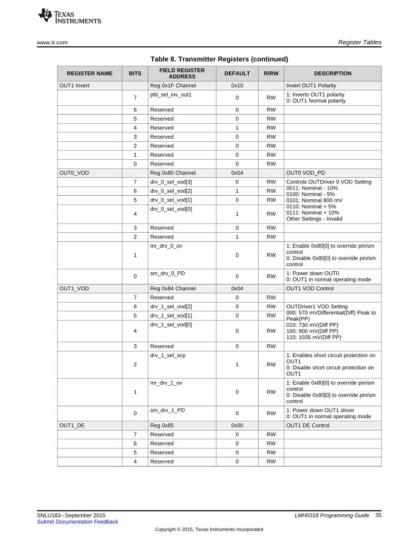
Table 8. Transmitter Registers
FIELD REGISTERREGISTER NAME BITS DEFAULT R/RW DESCRIPTIONADDRESSOut0_Mux_Select Reg 0x1C Channel 0x18 OUT0 Mux Selection
7 pfd_sel0_data_mux[2] 0 RW When 0x09[5] = 1'b OUT0 MuxSelection can be controlled as6 pfd_sel0_data_mux[1] 0 RW follows:
pfd_sel0_data_mux[0] 000: Mute001: 10 MHz Clock
5 0 RW 010: Raw Data100: Retimed DataOther Settings - Invalid
vco_clk_sel When 0x09[5] = 1'b and 0x1E[[7:5] =101'b OUT1 clock selection can be
4 1 RW controlled as follows:1: OUT1 puts out line rate clock0: OUT1 puts out 10MHz clock
3 mr_drv_out_ctrl[1] 1 RW Controls both OUT0 and OUT1:00:mr_drv_out_ctrl[0] OUT0: MuteOUT1: Mute01:OUT0: Locked Reclocked Data /Unlocked Raw DataOUT1: Locked Output Clock /Unlocked Mute
2 0 RW 10:OUT0: Locked Reclocked Data /Unlocked RAWOUT1: Locked Reclocked Data /Unlocked Raw11:OUT0: Forced RawOUT1: Forced Raw
1 Reserved 0 RW0 Reserved 0 RW
OUT1_Mux_Select Reg 0x1E Channel 0xE9 OUT1 Mux Selection7 pfd_sel_data_mux[2] 1 RW When 0x09[5] = 1'b OUT0 Mux
Selection can be controlled as6 pfd_sel_data_mux[1] 1 RW follows:pfd_sel_data_mux[0] 111: Mute
101: 10MHz Clock if reg 0x1c[4]=0and full rate clock if reg 0x1c[4] = 1
5 1 RW 010: Full Rate Clock001: Retimed Data000: Raw DataOther Settings - Invalid
4 Reserved 0 RW3 Reserved 1 RW2 Reserved 0 RW1 Reserved 0 RW0 Reserved 1 RW
34 LMH0318 Programming Guide SNLU183–September 2015Submit Documentation Feedback
Copyright © 2015, Texas Instruments Incorporated
www.ti.com Register Tables
Table 8. Transmitter Registers (continued)FIELD REGISTERREGISTER NAME BITS DEFAULT R/RW DESCRIPTIONADDRESS
OUT1 Invert Reg 0x1F Channel 0x10 Invert OUT1 Polaritypfd_sel_inv_out1 1: Inverts OUT1 polarity7 0 RW 0: OUT1 Normal polarity
6 Reserved 0 RW5 Reserved 0 RW4 Reserved 1 RW3 Reserved 0 RW2 Reserved 0 RW1 Reserved 0 RW0 Reserved 0 RW
OUT0_VOD Reg 0x80 Channel 0x54 OUT0 VOD_PD7 drv_0_sel_vod[3] 0 RW Controls OUTDriver 0 VOD Setting
0011: Nominal - 10%6 drv_0_sel_vod[2] 1 RW 0100: Nominal - 5%5 drv_0_sel_vod[1] 0 RW 0101: Nominal 800 mV
0110: Nominal + 5%drv_0_sel_vod[0]0111: Nominal + 10%4 1 RWOther Settings - Invalid
3 Reserved 0 RW2 Reserved 1 RW
mr_drv_0_ov 1: Enable 0x80[0] to override pin/smcontrol1 0 RW 0: Disable 0x80[0] to override pin/smcontrol
sm_drv_0_PD 1: Power down OUT00 0 RW 0: OUT1 in normal operating modeOUT1_VOD Reg 0x84 Channel 0x04 OUT1 VOD Control
7 Reserved 0 RW6 drv_1_sel_vod[2] 0 RW OUTDriver1 VOD Setting
000: 570 mVDifferential(Diff) Peak to5 drv_1_sel_vod[1] 0 RW Peak(PP)drv_1_sel_vod[0] 010: 730 mV(Diff PP)
4 0 RW 100: 900 mV(Diff PP)110: 1035 mV(Diff PP)
3 Reserved 0 RWdrv_1_sel_scp 1: Enables short circuit protection on
OUT12 1 RW 0: Disable short circuit protection onOUT1
mr_drv_1_ov 1: Enable 0x80[0] to override pin/smcontrol1 0 RW 0: Disable 0x80[0] to override pin/smcontrol
sm_drv_1_PD 1: Power down OUT1 driver0 0 RW 0: OUT1 in normal operating modeOUT1_DE Reg 0x85 0x00 OUT1 DE Control
7 Reserved 0 RW6 Reserved 0 RW5 Reserved 0 RW4 Reserved 0 RW
35SNLU183–September 2015 LMH0318 Programming GuideSubmit Documentation Feedback
Copyright © 2015, Texas Instruments Incorporated
Register Tables www.ti.com
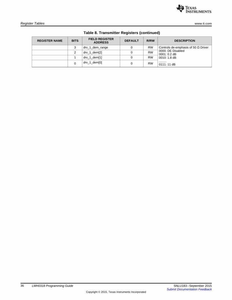
Table 8. Transmitter Registers (continued)FIELD REGISTERREGISTER NAME BITS DEFAULT R/RW DESCRIPTIONADDRESS
3 drv_1_dem_range 0 RW Controls de-emphasis of 50 Ω Driver0000: DE Disabled2 drv_1_dem[2] 0 RW 0001: 0.2 dB
1 drv_1_dem[1] 0 RW 0010: 1.8 dB.........drv_1_dem[0]0 0 RW 0111: 11 dB
36 LMH0318 Programming Guide SNLU183–September 2015Submit Documentation Feedback
Copyright © 2015, Texas Instruments Incorporated
STANDARD TERMS AND CONDITIONS FOR EVALUATION MODULES1. Delivery: TI delivers TI evaluation boards, kits, or modules, including any accompanying demonstration software, components, or
documentation (collectively, an “EVM” or “EVMs”) to the User (“User”) in accordance with the terms and conditions set forth herein.Acceptance of the EVM is expressly subject to the following terms and conditions.1.1 EVMs are intended solely for product or software developers for use in a research and development setting to facilitate feasibility
evaluation, experimentation, or scientific analysis of TI semiconductors products. EVMs have no direct function and are notfinished products. EVMs shall not be directly or indirectly assembled as a part or subassembly in any finished product. Forclarification, any software or software tools provided with the EVM (“Software”) shall not be subject to the terms and conditionsset forth herein but rather shall be subject to the applicable terms and conditions that accompany such Software
1.2 EVMs are not intended for consumer or household use. EVMs may not be sold, sublicensed, leased, rented, loaned, assigned,or otherwise distributed for commercial purposes by Users, in whole or in part, or used in any finished product or productionsystem.
2 Limited Warranty and Related Remedies/Disclaimers:2.1 These terms and conditions do not apply to Software. The warranty, if any, for Software is covered in the applicable Software
License Agreement.2.2 TI warrants that the TI EVM will conform to TI's published specifications for ninety (90) days after the date TI delivers such EVM
to User. Notwithstanding the foregoing, TI shall not be liable for any defects that are caused by neglect, misuse or mistreatmentby an entity other than TI, including improper installation or testing, or for any EVMs that have been altered or modified in anyway by an entity other than TI. Moreover, TI shall not be liable for any defects that result from User's design, specifications orinstructions for such EVMs. Testing and other quality control techniques are used to the extent TI deems necessary or asmandated by government requirements. TI does not test all parameters of each EVM.
2.3 If any EVM fails to conform to the warranty set forth above, TI's sole liability shall be at its option to repair or replace such EVM,or credit User's account for such EVM. TI's liability under this warranty shall be limited to EVMs that are returned during thewarranty period to the address designated by TI and that are determined by TI not to conform to such warranty. If TI elects torepair or replace such EVM, TI shall have a reasonable time to repair such EVM or provide replacements. Repaired EVMs shallbe warranted for the remainder of the original warranty period. Replaced EVMs shall be warranted for a new full ninety (90) daywarranty period.
3 Regulatory Notices:3.1 United States
3.1.1 Notice applicable to EVMs not FCC-Approved:This kit is designed to allow product developers to evaluate electronic components, circuitry, or software associated with the kitto determine whether to incorporate such items in a finished product and software developers to write software applications foruse with the end product. This kit is not a finished product and when assembled may not be resold or otherwise marketed unlessall required FCC equipment authorizations are first obtained. Operation is subject to the condition that this product not causeharmful interference to licensed radio stations and that this product accept harmful interference. Unless the assembled kit isdesigned to operate under part 15, part 18 or part 95 of this chapter, the operator of the kit must operate under the authority ofan FCC license holder or must secure an experimental authorization under part 5 of this chapter.3.1.2 For EVMs annotated as FCC – FEDERAL COMMUNICATIONS COMMISSION Part 15 Compliant:
CAUTIONThis device complies with part 15 of the FCC Rules. Operation is subject to the following two conditions: (1) This device may notcause harmful interference, and (2) this device must accept any interference received, including interference that may causeundesired operation.Changes or modifications not expressly approved by the party responsible for compliance could void the user's authority tooperate the equipment.
FCC Interference Statement for Class A EVM devicesNOTE: This equipment has been tested and found to comply with the limits for a Class A digital device, pursuant to part 15 ofthe FCC Rules. These limits are designed to provide reasonable protection against harmful interference when the equipment isoperated in a commercial environment. This equipment generates, uses, and can radiate radio frequency energy and, if notinstalled and used in accordance with the instruction manual, may cause harmful interference to radio communications.Operation of this equipment in a residential area is likely to cause harmful interference in which case the user will be required tocorrect the interference at his own expense.
SPACER
SPACER
SPACER
SPACER
SPACER
SPACER
SPACER
SPACER

FCC Interference Statement for Class B EVM devicesNOTE: This equipment has been tested and found to comply with the limits for a Class B digital device, pursuant to part 15 ofthe FCC Rules. These limits are designed to provide reasonable protection against harmful interference in a residentialinstallation. This equipment generates, uses and can radiate radio frequency energy and, if not installed and used in accordancewith the instructions, may cause harmful interference to radio communications. However, there is no guarantee that interferencewill not occur in a particular installation. If this equipment does cause harmful interference to radio or television reception, whichcan be determined by turning the equipment off and on, the user is encouraged to try to correct the interference by one or moreof the following measures:
• Reorient or relocate the receiving antenna.• Increase the separation between the equipment and receiver.• Connect the equipment into an outlet on a circuit different from that to which the receiver is connected.• Consult the dealer or an experienced radio/TV technician for help.
3.2 Canada3.2.1 For EVMs issued with an Industry Canada Certificate of Conformance to RSS-210
Concerning EVMs Including Radio Transmitters:This device complies with Industry Canada license-exempt RSS standard(s). Operation is subject to the following two conditions:(1) this device may not cause interference, and (2) this device must accept any interference, including interference that maycause undesired operation of the device.
Concernant les EVMs avec appareils radio:Le présent appareil est conforme aux CNR d'Industrie Canada applicables aux appareils radio exempts de licence. L'exploitationest autorisée aux deux conditions suivantes: (1) l'appareil ne doit pas produire de brouillage, et (2) l'utilisateur de l'appareil doitaccepter tout brouillage radioélectrique subi, même si le brouillage est susceptible d'en compromettre le fonctionnement.
Concerning EVMs Including Detachable Antennas:Under Industry Canada regulations, this radio transmitter may only operate using an antenna of a type and maximum (or lesser)gain approved for the transmitter by Industry Canada. To reduce potential radio interference to other users, the antenna typeand its gain should be so chosen that the equivalent isotropically radiated power (e.i.r.p.) is not more than that necessary forsuccessful communication. This radio transmitter has been approved by Industry Canada to operate with the antenna typeslisted in the user guide with the maximum permissible gain and required antenna impedance for each antenna type indicated.Antenna types not included in this list, having a gain greater than the maximum gain indicated for that type, are strictly prohibitedfor use with this device.
Concernant les EVMs avec antennes détachablesConformément à la réglementation d'Industrie Canada, le présent émetteur radio peut fonctionner avec une antenne d'un type etd'un gain maximal (ou inférieur) approuvé pour l'émetteur par Industrie Canada. Dans le but de réduire les risques de brouillageradioélectrique à l'intention des autres utilisateurs, il faut choisir le type d'antenne et son gain de sorte que la puissance isotroperayonnée équivalente (p.i.r.e.) ne dépasse pas l'intensité nécessaire à l'établissement d'une communication satisfaisante. Leprésent émetteur radio a été approuvé par Industrie Canada pour fonctionner avec les types d'antenne énumérés dans lemanuel d’usage et ayant un gain admissible maximal et l'impédance requise pour chaque type d'antenne. Les types d'antennenon inclus dans cette liste, ou dont le gain est supérieur au gain maximal indiqué, sont strictement interdits pour l'exploitation del'émetteur
3.3 Japan3.3.1 Notice for EVMs delivered in Japan: Please see http://www.tij.co.jp/lsds/ti_ja/general/eStore/notice_01.page 日本国内に
輸入される評価用キット、ボードについては、次のところをご覧ください。http://www.tij.co.jp/lsds/ti_ja/general/eStore/notice_01.page
3.3.2 Notice for Users of EVMs Considered “Radio Frequency Products” in Japan: EVMs entering Japan may not be certifiedby TI as conforming to Technical Regulations of Radio Law of Japan.
If User uses EVMs in Japan, not certified to Technical Regulations of Radio Law of Japan, User is required by Radio Law ofJapan to follow the instructions below with respect to EVMs:1. Use EVMs in a shielded room or any other test facility as defined in the notification #173 issued by Ministry of Internal
Affairs and Communications on March 28, 2006, based on Sub-section 1.1 of Article 6 of the Ministry’s Rule forEnforcement of Radio Law of Japan,
2. Use EVMs only after User obtains the license of Test Radio Station as provided in Radio Law of Japan with respect toEVMs, or
3. Use of EVMs only after User obtains the Technical Regulations Conformity Certification as provided in Radio Law of Japanwith respect to EVMs. Also, do not transfer EVMs, unless User gives the same notice above to the transferee. Please notethat if User does not follow the instructions above, User will be subject to penalties of Radio Law of Japan.
SPACER
SPACER
SPACER
SPACER
SPACER
【無線電波を送信する製品の開発キットをお使いになる際の注意事項】 開発キットの中には技術基準適合証明を受けていないものがあります。 技術適合証明を受けていないもののご使用に際しては、電波法遵守のため、以下のいずれかの措置を取っていただく必要がありますのでご注意ください。1. 電波法施行規則第6条第1項第1号に基づく平成18年3月28日総務省告示第173号で定められた電波暗室等の試験設備でご使用
いただく。2. 実験局の免許を取得後ご使用いただく。3. 技術基準適合証明を取得後ご使用いただく。
なお、本製品は、上記の「ご使用にあたっての注意」を譲渡先、移転先に通知しない限り、譲渡、移転できないものとします。上記を遵守頂けない場合は、電波法の罰則が適用される可能性があることをご留意ください。 日本テキサス・イ
ンスツルメンツ株式会社東京都新宿区西新宿6丁目24番1号西新宿三井ビル
3.3.3 Notice for EVMs for Power Line Communication: Please see http://www.tij.co.jp/lsds/ti_ja/general/eStore/notice_02.page電力線搬送波通信についての開発キットをお使いになる際の注意事項については、次のところをご覧ください。http://www.tij.co.jp/lsds/ti_ja/general/eStore/notice_02.page
SPACER4 EVM Use Restrictions and Warnings:
4.1 EVMS ARE NOT FOR USE IN FUNCTIONAL SAFETY AND/OR SAFETY CRITICAL EVALUATIONS, INCLUDING BUT NOTLIMITED TO EVALUATIONS OF LIFE SUPPORT APPLICATIONS.
4.2 User must read and apply the user guide and other available documentation provided by TI regarding the EVM prior to handlingor using the EVM, including without limitation any warning or restriction notices. The notices contain important safety informationrelated to, for example, temperatures and voltages.
4.3 Safety-Related Warnings and Restrictions:4.3.1 User shall operate the EVM within TI’s recommended specifications and environmental considerations stated in the user
guide, other available documentation provided by TI, and any other applicable requirements and employ reasonable andcustomary safeguards. Exceeding the specified performance ratings and specifications (including but not limited to inputand output voltage, current, power, and environmental ranges) for the EVM may cause personal injury or death, orproperty damage. If there are questions concerning performance ratings and specifications, User should contact a TIfield representative prior to connecting interface electronics including input power and intended loads. Any loads appliedoutside of the specified output range may also result in unintended and/or inaccurate operation and/or possiblepermanent damage to the EVM and/or interface electronics. Please consult the EVM user guide prior to connecting anyload to the EVM output. If there is uncertainty as to the load specification, please contact a TI field representative.During normal operation, even with the inputs and outputs kept within the specified allowable ranges, some circuitcomponents may have elevated case temperatures. These components include but are not limited to linear regulators,switching transistors, pass transistors, current sense resistors, and heat sinks, which can be identified using theinformation in the associated documentation. When working with the EVM, please be aware that the EVM may becomevery warm.
4.3.2 EVMs are intended solely for use by technically qualified, professional electronics experts who are familiar with thedangers and application risks associated with handling electrical mechanical components, systems, and subsystems.User assumes all responsibility and liability for proper and safe handling and use of the EVM by User or its employees,affiliates, contractors or designees. User assumes all responsibility and liability to ensure that any interfaces (electronicand/or mechanical) between the EVM and any human body are designed with suitable isolation and means to safelylimit accessible leakage currents to minimize the risk of electrical shock hazard. User assumes all responsibility andliability for any improper or unsafe handling or use of the EVM by User or its employees, affiliates, contractors ordesignees.
4.4 User assumes all responsibility and liability to determine whether the EVM is subject to any applicable international, federal,state, or local laws and regulations related to User’s handling and use of the EVM and, if applicable, User assumes allresponsibility and liability for compliance in all respects with such laws and regulations. User assumes all responsibility andliability for proper disposal and recycling of the EVM consistent with all applicable international, federal, state, and localrequirements.
5. Accuracy of Information: To the extent TI provides information on the availability and function of EVMs, TI attempts to be as accurateas possible. However, TI does not warrant the accuracy of EVM descriptions, EVM availability or other information on its websites asaccurate, complete, reliable, current, or error-free.
SPACER
SPACER
SPACER
SPACER
SPACER
SPACER
SPACER6. Disclaimers:
6.1 EXCEPT AS SET FORTH ABOVE, EVMS AND ANY WRITTEN DESIGN MATERIALS PROVIDED WITH THE EVM (AND THEDESIGN OF THE EVM ITSELF) ARE PROVIDED "AS IS" AND "WITH ALL FAULTS." TI DISCLAIMS ALL OTHERWARRANTIES, EXPRESS OR IMPLIED, REGARDING SUCH ITEMS, INCLUDING BUT NOT LIMITED TO ANY IMPLIEDWARRANTIES OF MERCHANTABILITY OR FITNESS FOR A PARTICULAR PURPOSE OR NON-INFRINGEMENT OF ANYTHIRD PARTY PATENTS, COPYRIGHTS, TRADE SECRETS OR OTHER INTELLECTUAL PROPERTY RIGHTS.
6.2 EXCEPT FOR THE LIMITED RIGHT TO USE THE EVM SET FORTH HEREIN, NOTHING IN THESE TERMS ANDCONDITIONS SHALL BE CONSTRUED AS GRANTING OR CONFERRING ANY RIGHTS BY LICENSE, PATENT, OR ANYOTHER INDUSTRIAL OR INTELLECTUAL PROPERTY RIGHT OF TI, ITS SUPPLIERS/LICENSORS OR ANY OTHER THIRDPARTY, TO USE THE EVM IN ANY FINISHED END-USER OR READY-TO-USE FINAL PRODUCT, OR FOR ANYINVENTION, DISCOVERY OR IMPROVEMENT MADE, CONCEIVED OR ACQUIRED PRIOR TO OR AFTER DELIVERY OFTHE EVM.
7. USER'S INDEMNITY OBLIGATIONS AND REPRESENTATIONS. USER WILL DEFEND, INDEMNIFY AND HOLD TI, ITSLICENSORS AND THEIR REPRESENTATIVES HARMLESS FROM AND AGAINST ANY AND ALL CLAIMS, DAMAGES, LOSSES,EXPENSES, COSTS AND LIABILITIES (COLLECTIVELY, "CLAIMS") ARISING OUT OF OR IN CONNECTION WITH ANYHANDLING OR USE OF THE EVM THAT IS NOT IN ACCORDANCE WITH THESE TERMS AND CONDITIONS. THIS OBLIGATIONSHALL APPLY WHETHER CLAIMS ARISE UNDER STATUTE, REGULATION, OR THE LAW OF TORT, CONTRACT OR ANYOTHER LEGAL THEORY, AND EVEN IF THE EVM FAILS TO PERFORM AS DESCRIBED OR EXPECTED.
8. Limitations on Damages and Liability:8.1 General Limitations. IN NO EVENT SHALL TI BE LIABLE FOR ANY SPECIAL, COLLATERAL, INDIRECT, PUNITIVE,
INCIDENTAL, CONSEQUENTIAL, OR EXEMPLARY DAMAGES IN CONNECTION WITH OR ARISING OUT OF THESETERMS ANDCONDITIONS OR THE USE OF THE EVMS PROVIDED HEREUNDER, REGARDLESS OF WHETHER TI HASBEEN ADVISED OF THE POSSIBILITY OF SUCH DAMAGES. EXCLUDED DAMAGES INCLUDE, BUT ARE NOT LIMITEDTO, COST OF REMOVAL OR REINSTALLATION, ANCILLARY COSTS TO THE PROCUREMENT OF SUBSTITUTE GOODSOR SERVICES, RETESTING, OUTSIDE COMPUTER TIME, LABOR COSTS, LOSS OF GOODWILL, LOSS OF PROFITS,LOSS OF SAVINGS, LOSS OF USE, LOSS OF DATA, OR BUSINESS INTERRUPTION. NO CLAIM, SUIT OR ACTION SHALLBE BROUGHT AGAINST TI MORE THAN ONE YEAR AFTER THE RELATED CAUSE OF ACTION HAS OCCURRED.
8.2 Specific Limitations. IN NO EVENT SHALL TI'S AGGREGATE LIABILITY FROM ANY WARRANTY OR OTHER OBLIGATIONARISING OUT OF OR IN CONNECTION WITH THESE TERMS AND CONDITIONS, OR ANY USE OF ANY TI EVMPROVIDED HEREUNDER, EXCEED THE TOTAL AMOUNT PAID TO TI FOR THE PARTICULAR UNITS SOLD UNDERTHESE TERMS AND CONDITIONS WITH RESPECT TO WHICH LOSSES OR DAMAGES ARE CLAIMED. THE EXISTENCEOF MORE THAN ONE CLAIM AGAINST THE PARTICULAR UNITS SOLD TO USER UNDER THESE TERMS ANDCONDITIONS SHALL NOT ENLARGE OR EXTEND THIS LIMIT.
9. Return Policy. Except as otherwise provided, TI does not offer any refunds, returns, or exchanges. Furthermore, no return of EVM(s)will be accepted if the package has been opened and no return of the EVM(s) will be accepted if they are damaged or otherwise not ina resalable condition. If User feels it has been incorrectly charged for the EVM(s) it ordered or that delivery violates the applicableorder, User should contact TI. All refunds will be made in full within thirty (30) working days from the return of the components(s),excluding any postage or packaging costs.
10. Governing Law: These terms and conditions shall be governed by and interpreted in accordance with the laws of the State of Texas,without reference to conflict-of-laws principles. User agrees that non-exclusive jurisdiction for any dispute arising out of or relating tothese terms and conditions lies within courts located in the State of Texas and consents to venue in Dallas County, Texas.Notwithstanding the foregoing, any judgment may be enforced in any United States or foreign court, and TI may seek injunctive reliefin any United States or foreign court.
Mailing Address: Texas Instruments, Post Office Box 655303, Dallas, Texas 75265Copyright © 2015, Texas Instruments Incorporated
spacer

IMPORTANT NOTICE
Texas Instruments Incorporated and its subsidiaries (TI) reserve the right to make corrections, enhancements, improvements and otherchanges to its semiconductor products and services per JESD46, latest issue, and to discontinue any product or service per JESD48, latestissue. Buyers should obtain the latest relevant information before placing orders and should verify that such information is current andcomplete. All semiconductor products (also referred to herein as “components”) are sold subject to TI’s terms and conditions of salesupplied at the time of order acknowledgment.TI warrants performance of its components to the specifications applicable at the time of sale, in accordance with the warranty in TI’s termsand conditions of sale of semiconductor products. Testing and other quality control techniques are used to the extent TI deems necessaryto support this warranty. Except where mandated by applicable law, testing of all parameters of each component is not necessarilyperformed.TI assumes no liability for applications assistance or the design of Buyers’ products. Buyers are responsible for their products andapplications using TI components. To minimize the risks associated with Buyers’ products and applications, Buyers should provideadequate design and operating safeguards.TI does not warrant or represent that any license, either express or implied, is granted under any patent right, copyright, mask work right, orother intellectual property right relating to any combination, machine, or process in which TI components or services are used. Informationpublished by TI regarding third-party products or services does not constitute a license to use such products or services or a warranty orendorsement thereof. Use of such information may require a license from a third party under the patents or other intellectual property of thethird party, or a license from TI under the patents or other intellectual property of TI.Reproduction of significant portions of TI information in TI data books or data sheets is permissible only if reproduction is without alterationand is accompanied by all associated warranties, conditions, limitations, and notices. TI is not responsible or liable for such altereddocumentation. Information of third parties may be subject to additional restrictions.Resale of TI components or services with statements different from or beyond the parameters stated by TI for that component or servicevoids all express and any implied warranties for the associated TI component or service and is an unfair and deceptive business practice.TI is not responsible or liable for any such statements.Buyer acknowledges and agrees that it is solely responsible for compliance with all legal, regulatory and safety-related requirementsconcerning its products, and any use of TI components in its applications, notwithstanding any applications-related information or supportthat may be provided by TI. Buyer represents and agrees that it has all the necessary expertise to create and implement safeguards whichanticipate dangerous consequences of failures, monitor failures and their consequences, lessen the likelihood of failures that might causeharm and take appropriate remedial actions. Buyer will fully indemnify TI and its representatives against any damages arising out of the useof any TI components in safety-critical applications.In some cases, TI components may be promoted specifically to facilitate safety-related applications. With such components, TI’s goal is tohelp enable customers to design and create their own end-product solutions that meet applicable functional safety standards andrequirements. Nonetheless, such components are subject to these terms.No TI components are authorized for use in FDA Class III (or similar life-critical medical equipment) unless authorized officers of the partieshave executed a special agreement specifically governing such use.Only those TI components which TI has specifically designated as military grade or “enhanced plastic” are designed and intended for use inmilitary/aerospace applications or environments. Buyer acknowledges and agrees that any military or aerospace use of TI componentswhich have not been so designated is solely at the Buyer's risk, and that Buyer is solely responsible for compliance with all legal andregulatory requirements in connection with such use.TI has specifically designated certain components as meeting ISO/TS16949 requirements, mainly for automotive use. In any case of use ofnon-designated products, TI will not be responsible for any failure to meet ISO/TS16949.
Products ApplicationsAudio www.ti.com/audio Automotive and Transportation www.ti.com/automotiveAmplifiers amplifier.ti.com Communications and Telecom www.ti.com/communicationsData Converters dataconverter.ti.com Computers and Peripherals www.ti.com/computersDLP® Products www.dlp.com Consumer Electronics www.ti.com/consumer-appsDSP dsp.ti.com Energy and Lighting www.ti.com/energyClocks and Timers www.ti.com/clocks Industrial www.ti.com/industrialInterface interface.ti.com Medical www.ti.com/medicalLogic logic.ti.com Security www.ti.com/securityPower Mgmt power.ti.com Space, Avionics and Defense www.ti.com/space-avionics-defenseMicrocontrollers microcontroller.ti.com Video and Imaging www.ti.com/videoRFID www.ti-rfid.comOMAP Applications Processors www.ti.com/omap TI E2E Community e2e.ti.comWireless Connectivity www.ti.com/wirelessconnectivity
Mailing Address: Texas Instruments, Post Office Box 655303, Dallas, Texas 75265Copyright © 2015, Texas Instruments Incorporated