hd3ss3415 4-channel high-performance differential · pdf filegnd top view rua package 1 38 2 1...
TRANSCRIPT

GND
Top View
RUA
Package
1 38
22
21
18
17
42
39
A2+
C1+
A2-
C2+
A1+
C2-
C3+
C3-
A0-
GN
D
GN
D
GN
D
VD
D
VDD
VDD
NC
SEL
GND
B2-
B1+
B1-
B3+
B3-
NC
GN
D
NC
GND
VDD
NC
VD
D
GND
B0+
B0-
NC
B2+
C1-
A0+
C0+
C0-
A1-
A3+
A3-
Product
Folder
Sample &Buy
Technical
Documents
Tools &
Software
Support &Community
HD3SS3415SLAS840C –MARCH 2012–REVISED OCTOBER 2015
HD3SS3415 4-Channel High-Performance Differential Switch1 Features 3 Description
The HD3SS3415 is a high-speed passive switch1• Compatible with Multiple Interface Standards
capable of switching four differential channels,Operating up to 12 Gbps Including PCI Expressincluding applications such as two full PCI Express x1Gen III and USB 3.0 lanes from one source to one of two target locations
• Wide –3-dB Differential BW of over 8 GHz in a PC/server application. With its bidirectionalcapability the HD3SS3415 will also support• Excellent Dynamic Characteristics (at 4 GHz)applications that allow connections between one– Crosstalk = –35 dBtarget and two source devices, such as a shared
– Off Isolation = –19 dB peripheral between two platforms. The HD3SS3415– Insertion Loss = –1.5 dB has a single control line (SEL Pin) which can be used
to control the signal path between Port A and either– Return Loss = –11 dBPort B or Port C.• VDD Operating Range 3.3 V ±10%The HD3SS3415 is offered in an industry standard• Small 3.5 mm × 9 mm, 42-Pin WQFN Package42-pin WQFN package available in a common
• Common Industry Standard Pinout footprint shared by several other vendors. The deviceis specified to operate from a single supply voltage of
2 Applications 3.3 V over the full temperature range of 0°C to 70°C• Desktop and Notebook PCs
Device Information(1)• Server/Storage Area Networks
PART NUMBER PACKAGE BODY SIZE (NOM)• PCI Express Backplanes
HD3SS3415 WQFN (42) 9.00 mm × 3.50 mm• Shared I/O Ports
(1) For all available packages, see the orderable addendum atthe end of the datasheet.
HD3SS3415 Pinout HD3SS3415 Switch Flow Through Routing
1
An IMPORTANT NOTICE at the end of this data sheet addresses availability, warranty, changes, use in safety-critical applications,intellectual property matters and other important disclaimers. PRODUCTION DATA.

HD3SS3415SLAS840C –MARCH 2012–REVISED OCTOBER 2015 www.ti.com
Table of Contents9.2 Functional Block Diagram ....................................... 121 Features .................................................................. 19.3 Feature Description................................................. 132 Applications ........................................................... 19.4 Device Functional Modes........................................ 133 Description ............................................................. 1
10 Application and Implementation........................ 144 Revision History..................................................... 210.1 Application Information.......................................... 145 Description continued ........................................... 310.2 Typical Application ............................................... 156 Pin Configuration and Functions ......................... 4
11 Power Supply Recommendations ..................... 177 Specifications......................................................... 612 Layout................................................................... 177.1 Absolute Maximum Ratings ...................................... 6
12.1 Layout Guidelines ................................................. 177.2 ESD Ratings.............................................................. 612.2 Layout Example .................................................... 177.3 Recommended Operating Conditions....................... 6
13 Device and Documentation Support ................. 187.4 Thermal Information .................................................. 613.1 Community Resources.......................................... 187.5 Electrical Characteristics........................................... 713.2 Trademarks ........................................................... 187.6 Dissipation Ratings ................................................... 713.3 Electrostatic Discharge Caution............................ 187.7 Typical Characteristics .............................................. 913.4 Glossary ................................................................ 188 Parameter Measurement Information ................ 10
14 Mechanical, Packaging, and Orderable9 Detailed Description ............................................ 12 Information ........................................................... 189.1 Overview ................................................................. 12
4 Revision HistoryNOTE: Page numbers for previous revisions may differ from page numbers in the current version.
Changes from Revision B (August 2015) to Revision C Page
• Changed the HD3SS3415 Pinout and HD3SS3415 Switch Flow Through Routing images.................................................. 1• Changed temperature From: industrial temperature range of –40°C to 85°C To: industrial temperature range of 0°C
to 70°C in the Overview section ........................................................................................................................................... 12
Changes from Revision A (July 2015) to Revision B Page
• Changed the Storage temperature MIN value From: 65 To: –65 in the Absolute Maximum Ratings (1) (2) table ................... 6
Changes from Original (February 2012 ) to Revision A Page
• Added Pin Configuration and Functions section, ESD Ratings table, Feature Description section, Device FunctionalModes, Application and Implementation section, Power Supply Recommendations section, Layout section, Deviceand Documentation Support section, and Mechanical, Packaging, and Orderable Information section .............................. 1
• Deleted the word "industrial" from Description section........................................................................................................... 1• Changed the second paragraph of the Description -40 to 0 and 85 to 70°C ......................................................................... 1• Changed TA spec values from –40°C MIN and 85°C MAX to 0°C MIN and 70°C MAX in the Recommended
Operating Conditions table. .................................................................................................................................................... 6
2 Submit Documentation Feedback Copyright © 2012–2015, Texas Instruments Incorporated
Product Folder Links: HD3SS3415
HD3SS3415www.ti.com SLAS840C –MARCH 2012–REVISED OCTOBER 2015
5 Description continuedThe HD3SS3415 is a generic 4-CH high-speed mux/demux type of switch that can be used for routing high-speed signals between two different locations on a circuit board. Although it was designed specifically to addressPCI Express Gen III applications, the HD3SS3415 will also support several other high-speed data protocols witha differential amplitude of < 1800 mVpp and a common mode voltage of < 2 V, as with USB 3.0 and DisplayPort1.2. The one select input (SEL) pin of the device can easily be controlled by an available GPIO pin within asystem or from a microcontroller.
Copyright © 2012–2015, Texas Instruments Incorporated Submit Documentation Feedback 3
Product Folder Links: HD3SS3415

GND
Top View
RUA
Package
1 38
22
21
18
17
42
39
A2+
C1+
A2-
C2+
A1+
C2-
C3+
C3-
A0-
GN
D
GN
D
GN
D
VD
D
VDD
VDD
NC
SEL
GND
B2-
B1+
B1-
B3+
B3-
NC
GN
D
NC
GND
VDD
NC
VD
D
GND
B0+
B0-
NC
B2+
C1-
A0+
C0+
C0-
A1-
A3+
A3-
HD3SS3415SLAS840C –MARCH 2012–REVISED OCTOBER 2015 www.ti.com
6 Pin Configuration and Functions
RUA Package42-Pin WQFN
Top View
Pin FunctionsPIN
I/O DESCRIPTIONNAME NO.SWITCH PORT AA0+ 1 Port A, Channel 0, High Speed Positive SignalA0– 2 Port A, Channel 0, High Speed Negative SignalA1+ 5 Port A, Channel 1, High Speed Positive SignalA1– 6 Port A, Channel 1, High Speed Negative Signal
I/OA2+ 10 Port A, Channel 2, High Speed Positive SignalA2– 11 Port A, Channel 2, High Speed Negative SignalA3+ 14 Port A, Channel 3, High Speed Positive SignalA3– 15 Port A, Channel 3, High Speed Negative SignalSWITCH PORT BB0+ 37 Port B, Channel 0, High Speed Positive SignalB0– 36 lPort B, Channel 0, High Speed Negative SignalB1+ 33 Port B, Channel 1, High Speed Positive SignalB1– 32 Port B, Channel 1, High Speed Negative Signal
I/OB2+ 28 Port B, Channel 2, High Speed Positive SignalB2– 27 Port B, Channel 2, High Speed Negative SignalB3+ 24 Port B, Channel 3, High Speed Positive SignalB3– 23 Port B, Channel 3, High Speed Negative Signal
4 Submit Documentation Feedback Copyright © 2012–2015, Texas Instruments Incorporated
Product Folder Links: HD3SS3415
HD3SS3415www.ti.com SLAS840C –MARCH 2012–REVISED OCTOBER 2015
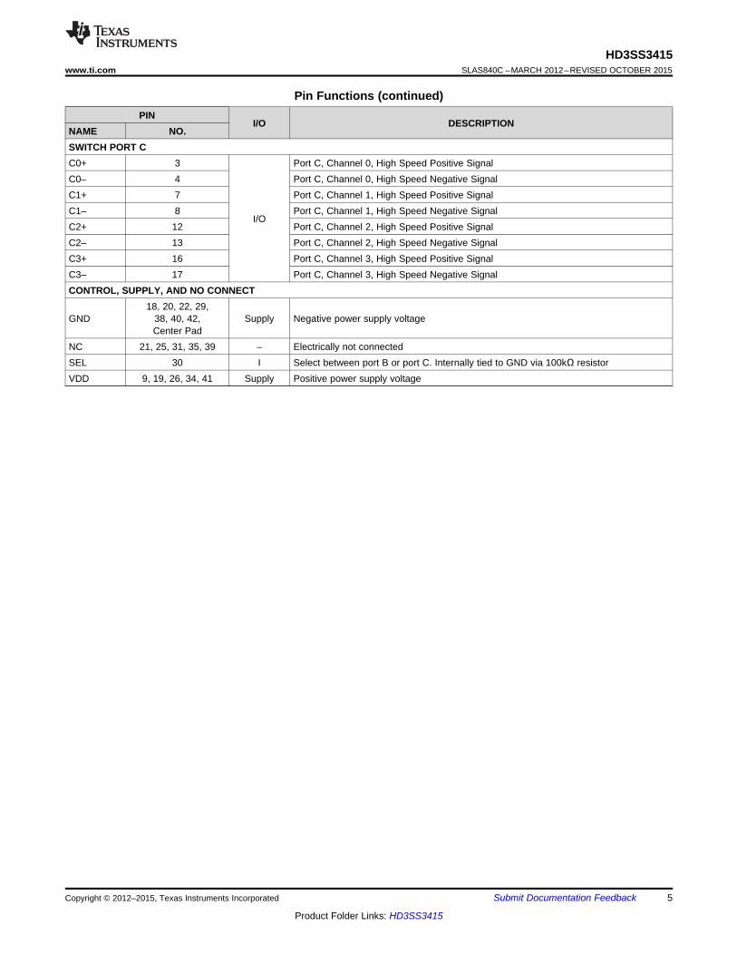
Pin Functions (continued)PIN
I/O DESCRIPTIONNAME NO.SWITCH PORT CC0+ 3 Port C, Channel 0, High Speed Positive SignalC0– 4 Port C, Channel 0, High Speed Negative SignalC1+ 7 Port C, Channel 1, High Speed Positive SignalC1– 8 Port C, Channel 1, High Speed Negative Signal
I/OC2+ 12 Port C, Channel 2, High Speed Positive SignalC2– 13 Port C, Channel 2, High Speed Negative SignalC3+ 16 Port C, Channel 3, High Speed Positive SignalC3– 17 Port C, Channel 3, High Speed Negative SignalCONTROL, SUPPLY, AND NO CONNECT
18, 20, 22, 29,GND 38, 40, 42, Supply Negative power supply voltage
Center PadNC 21, 25, 31, 35, 39 – Electrically not connectedSEL 30 I Select between port B or port C. Internally tied to GND via 100kΩ resistorVDD 9, 19, 26, 34, 41 Supply Positive power supply voltage
Copyright © 2012–2015, Texas Instruments Incorporated Submit Documentation Feedback 5
Product Folder Links: HD3SS3415

HD3SS3415SLAS840C –MARCH 2012–REVISED OCTOBER 2015 www.ti.com
7 Specifications
7.1 Absolute Maximum Ratings (1) (2)
Over operating free-air temperature range (unless otherwise noted)MIN MAX UNIT
Supply voltage (VDD) Absolute minimum/maximum supply voltage range –0.5 4 VDifferential I/O –0.5 4
Voltage VControl pin (SEL) –0.5 VDD+0.5
Storage temperature (Tstg) –65 150 ºC
(1) Stresses beyond those listed under absolute maximum ratings may cause permanent damage to the device. These are stress ratingsonly and functional operation of the device at these or any conditions beyond those indicated under recommended operating conditionsis not implied. Exposure to absolute-maximum-rated conditions for extended periods may affect device reliability.
(2) All voltage values, except differential voltages, are with respect to network ground terminal.
7.2 ESD RatingsVALUE UNIT
Human body model (HBM), per ANSI/ESDA/JEDEC JS-001 (1) ±4000V(ESD) Electrostatic discharge VCharged-device model (CDM), per JEDEC specification JESD22- ±1500C101 (2)
(1) JEDEC document JEP155 states that 500-V HBM allows safe manufacturing with a standard ESD control process.(2) JEDEC document JEP157 states that 250-V CDM allows safe manufacturing with a standard ESD control process.
7.3 Recommended Operating ConditionsTypical values for all parameters are at VDD = 3.3V and TA = 25°C. (Temperature limits are specified by design)
MIN TYP MAX UNITVDD Supply voltage 3.0 3.3 3.6 VVIH Input high voltage (SEL Pin) 2.0 VDD VVIL Input low voltage (SEL Pin) –0.1 0.8 VVI/O_Diff Differential voltage (differential pins) Switch I/O diff voltage 0 1.8 VPPVI/O_CM Common voltage (differential pins) Switch I/O common mode voltage 0 2.0 VTA Operating free-air temperature Ambient temperature 0 70 °C
7.4 Thermal InformationHD3SS3415
THERMAL METRIC (1) TQFN (RUA) UNIT42 PINS
RθJA Junction-to-ambient thermal resistance 53.8 °C/WRθJC(top) Junction-to-case (top) thermal resistance 38.2 °C/WRθJB Junction-to-board thermal resistance 21.9 °C/WψJT Junction-to-top characterization parameter 27.4 °C/WψJB Junction-to-board characterization parameter 5.6 °C/WRθJC(bot) Junction-to-case (bottom) thermal resistance 27.3 °C/W
(1) For more information about traditional and new thermal metrics, see the Semiconductor and IC Package Thermal Metrics applicationreport, SPRA953.
6 Submit Documentation Feedback Copyright © 2012–2015, Texas Instruments Incorporated
Product Folder Links: HD3SS3415

HD3SS3415www.ti.com SLAS840C –MARCH 2012–REVISED OCTOBER 2015
7.5 Electrical CharacteristicsRSC and RLOAD = 50 Ω and CL = 50 pF, over operating free-air temperature range (unless otherwise noted)
PARAMETER TEST CONDITIONS MIN TYP MAX UNIT
DEVICE PARAMETERS
IIH Input High Voltage (SEL) VDD = 3.6 V; VIN = VDD 95 µA
IIL Input Low Voltage (SEL) VDD = 3.6 V; VIN = GND 1 µA
VDD = 3.6 V; VIN = 0 V; VOUT = 2 V 130(ILK On OPEN outputs) [Ports B and C]Leakage Current (Differential I/OILK µApins) VDD = 3.6 V, VIN = 2 V; VOUT = 0 V 4(ILK On OPEN outputs) [Port A]
IDD Supply Current VDD = 3.6 V; SEL = VDD/GND; Outputs Floating 4.7 6 mA
CON Outputs ON Capacitance VIN = 0 V; Outputs Open; Switch ON 1.5 pF
COFF Outputs OFF Capacitance VIN = 0 V; Outputs Open, Switch OFF 1 pF
RON Output ON resistance VDD = 3.3 V; VCM = 0.5 V to 1.5 V ; IO = –8 mA 5 8 Ω
On resistance match between VDD = 3.3 V ; –0.35 V ≤ VIN ≤ 1.2 V; IO = –8 mA 2 ΩchannelsΔRON
On resistance match between pairs VDD = 3.3 V; –0.35 V ≤ VIN ≤ 1.2 V; IO = –8 mA 0.7 Ωof the same channel
On resistance flatnessRFLAT_ON VDD = 3.3 V; –0.35 V ≤ VIN ≤ 1.2 V 1.15 Ω(RON(MAX) – RON(MAIN)
tPD Switch propagation delay Rsc and RLOAD = 50 Ω 85 ps
SEL-to-switch Ton 70 250Rsc and RLOAD = 50 Ω ns
SEL-to-switch Toff 70 250
TSKEW_Inter Inter-pair output skew (CH-CH) 20 psRsc and RLOAD = 50 Ω
TSKEW_Intra Intra-pair output skew (bit-bit) 8 ps
f = 0.3 MHz –28Differential return loss (VCM = 0 V)RL f = 2500 MHz –12 dBSee Typical Characteristics
f = 4000 MHz –11
f = 0.3 MHz –90Differential Crosstalk(VCM = 0 V)XTALK f = 2500 MHz –39 dBSee Typical Characteristics
f = 4000 MHz –35
f = 0.3 MHz –75Differential Off-Isolation(VCM = 0 V)OIRR f = 2500 MHz –22 dBSee Typical Characteristics
f = 4000 MHz –19
f = 0.3 MHz –0.5Differential Insertion Loss (VCM = 0V)IL f = 2500 MHz –1.1 dBSee Typical Characteristics f = 4000 MHz –1.5
BW Band Width At –3 dB 8 GHz
7.6 Dissipation RatingsMIN MAX UNIT
PD Power Dissipation 15.5 21.6 mW
Copyright © 2012–2015, Texas Instruments Incorporated Submit Documentation Feedback 7
Product Folder Links: HD3SS3415

An+
An-
SEL
VDD
R = 50SC
W
R = 50SC
W
R = 50L
W
R = 50L
W
Bn+/Cn+
Bn-/Cn-
50%
50%
50%
50%
0V
0V
50%
50%
50%
50%
0V
0V
VDD
VDD
VDD
VDD
V +IN
V -IN
V +OUT
V +OUT
tP1 t
P1
HD
3S
S3415
SEL
VOUT
90%
10%
50%
Ton Toff
HD3SS3415SLAS840C –MARCH 2012–REVISED OCTOBER 2015 www.ti.com
Figure 1. Select to Switch Output On (TON) and Off (TOFF) Timing Diagram
TSKEWInter = Difference between tPD for any two pairs of outputsTSKEWIntra = Difference between tP1 and tP2 of same pair
Figure 2. Propagation Delay Timing Diagram and Test Setup
8 Submit Documentation Feedback Copyright © 2012–2015, Texas Instruments Incorporated
Product Folder Links: HD3SS3415

m1freq=dB(SDD21)=-86.588
300.0kHz
m2freq=dB(SDD21)=-33.793
2.514GHz
m3freq=dB(SDD21)=-29.900
3.985GHz
1E
7
1E
8
1E
9
1E
10
1E
6
2E
10
-100
-80
-60
-40
-20
-120
0
freq, Hz
dB
(S
DD
21
)
m1
m2m3
m1freq=dB(SDD21)=-86.588
300.0kHz
m2freq=dB(SDD21)=-33.793
2.514GHz
m3freq=dB(SDD21)=-29.900
3.985GHz
m1freq=dB(SDD21)=-78.265
300.0kHz
m2freq=dB(SDD21)=-22.547
2.514GHz
m3freq=dB(SDD21)=-19.244
3.985GHz
1E
7
1E
8
1E
9
1E
10
1E
6
2E
10
-80
-60
-40
-20
-100
0
freq, Hz
dB
(S
DD
21
)
m1
m2m3m1freq=dB(SDD21)=-78.265
300.0kHz
m2freq=dB(SDD21)=-22.547
2.514GHz
m3freq=dB(SDD21)=-19.244
3.985GHz
m5freq=dB(SDD11)=-28.295
300.0kHz
m6freq=dB(SDD11)=-13.591
2.514GHz
m7freq=dB(SDD11)=-10.275
3.985GHz
1E
7
1E
8
1E
9
1E
10
1E
6
2E
10
-25
-20
-15
-10
-5
0
-30
5
freq, Hz
dB
(S
DD
11
)
m5
m6
m7
m5freq=dB(SDD11)=-28.295
300.0kHz
m6freq=dB(SDD11)=-13.591
2.514GHz
m7freq=dB(SDD11)=-10.275
3.985GHz
m1freq=dB(SDD21)=-0.361
300.0kHz
m2freq=dB(SDD21)=-0.951
2.514GHz
m3freq=dB(SDD21)=-1.413
3.985GHz
m4freq=dB(SDD21)=-3.019
8.724GHz
1E
7
1E
8
1E
9
1E
10
1E
6
2E
10
-15
-10
-5
-20
0
freq, Hz
dB
(SD
D2
1)
m1 m2m3m4 m1
freq=dB(SDD21)=-0.361
300.0kHz
m2freq=dB(SDD21)=-0.951
2.514GHz
m3freq=dB(SDD21)=-1.413
3.985GHz
m4freq=dB(SDD21)=-3.019
8.724GHz
HD3SS3415www.ti.com SLAS840C –MARCH 2012–REVISED OCTOBER 2015
7.7 Typical Characteristics
Figure 3. Differential Insertion Loss Figure 4. Differential Return Loss
Figure 5. Differential Crosstalk Figure 6. Differential Off Isolation
Copyright © 2012–2015, Texas Instruments Incorporated Submit Documentation Feedback 9
Product Folder Links: HD3SS3415

A0+
A0-
B0+
B0-
B1+
B1-
Network
Analyzer
HD3SS3415
VDD
P1 P2
SEL
100 W
A0+
A0-
B0+
B0-
B1+
B1-
A1+
A1-
Network
Analyzer
HD3SS3415
VDD
P1 P2
SEL
100 W
100 W
HD3SS3415SLAS840C –MARCH 2012–REVISED OCTOBER 2015 www.ti.com
8 Parameter Measurement Information
Figure 7. Cross Talk Measurement Setup
Figure 8. Off Isolation Measurement Setup
10 Submit Documentation Feedback Copyright © 2012–2015, Texas Instruments Incorporated
Product Folder Links: HD3SS3415

Oscilloscope
1.4 Inches
Rogers
Microstrip
A
1.7 Inches
Rogers
Microstrip
10Gbps PRBS 27-1
Vi=0.8Vpp ; Vcm =0V
Oscilloscope10Gbps PRBS 27-1
Vi=0.8Vpp ; Vcm =0V
3.1 Inches Rogers
Microstrip
A
HD3SS3415www.ti.com SLAS840C –MARCH 2012–REVISED OCTOBER 2015
Parameter Measurement Information (continued)
Figure 9. Source Eye Diagram Test Setup
Figure 10. Output Eye Diagram Test Setup
Copyright © 2012–2015, Texas Instruments Incorporated Submit Documentation Feedback 11
Product Folder Links: HD3SS3415

SEL
VDD
GND
B0+
SEL
SEL
SEL
SEL
MU
X0
MU
X1
MU
X2
MU
X3
B0-
C0+
C0-
A0+
A0-
A1+
A1-
A2+
A2-
A3+
A3-
100kO
B1+
B1-
C1+
C1-
B3+
B3-
C3+
C3-
B2+
B2-
C2+
C2-
HD3SS3415SLAS840C –MARCH 2012–REVISED OCTOBER 2015 www.ti.com
9 Detailed Description
9.1 OverviewThe HD3SS3415 is a high-speed passive switch offered in an industry standard 42-pin WQFN package availablein a common footprint shared by several other vendors. The device is specified to operate from a single supplyvoltage of 3.3 V over the full industrial temperature range of 0°C to 70°C. The HD3SS3415 is a generic 4-CHhigh-speed mux/demux type of switch that can be used for routing high-speed signals between two differentlocations on a circuit board. Although it was designed specifically to address PCI Express Gen III applications,the HD3SS3415 will also support several other high-speed data protocols with a differential amplitude of < 1800mVpp and a common-mode voltage of < 2.0 V, as with USB 3.0 and DisplayPort 1.2.
9.2 Functional Block Diagram
12 Submit Documentation Feedback Copyright © 2012–2015, Texas Instruments Incorporated
Product Folder Links: HD3SS3415

HD3SS3415www.ti.com SLAS840C –MARCH 2012–REVISED OCTOBER 2015
9.3 Feature DescriptionThe HD3SS3415 has a single control line (SEL Pin) which can be used to control the signal path between Port Aand either Port B or Port C. Theone select input (SEL) pin of the device can easily be controlled by an availableGPIO pin within a system or from a microcontroller.
Table 1. MUX Pin Connections (1)
PORT B OR PORT C CHANNELCONNECTED TO PORT A CHANNELPORT A CHANNEL
SEL = L SEL = HA0+ B0+ C0+A0– B0– C0–A1+ B1+ C1+A1– B1– C1–A2+ B2+ C2+A2– B2– C2–A3+ B3+ C3+A3– B3– C3–
(1) The HD3SS3415 can tolerate polarity inversions for all differential signals on Ports A, B and C. Careshould be taken to ensure the same polarity is maintained on Port A vs. Port B/C.
9.4 Device Functional ModesTable 2 lists the functional modes for the HD3SS3415.
Table 2. HD3SS3415 Control LogicCONTROL PIN (SEL) PORT A TO PORT B CONNECTION STATUS PORT A TO PORT C CONNECTION STATUS
L (Default State) Connected DisconnectedH Disconnected Connected
Copyright © 2012–2015, Texas Instruments Incorporated Submit Documentation Feedback 13
Product Folder Links: HD3SS3415

HD3SS3415SLAS840C –MARCH 2012–REVISED OCTOBER 2015 www.ti.com
10 Application and Implementation
NOTEInformation in the following applications sections is not part of the TI componentspecification, and TI does not warrant its accuracy or completeness. TI’s customers areresponsible for determining suitability of components for their purposes. Customers shouldvalidate and test their design implementation to confirm system functionality.
10.1 Application Information
10.1.1 AC Coupling CapsMany interfaces require AC coupling between the transmitter and receiver. The 0402 capacitors are the preferredoption to provide AC coupling, and the 0603 size capacitors also work. The 0805 size capacitors and C-packsshould be avoided. When placing AC coupling capacitors symmetric placement is best. A capacitor value of 0.1µF is best and the value should be match for the ± signal pair. The placement should be along the TX pairs onthe system board, which are usually routed on the top layer of the board.
There are several placement options for the AC coupling capacitors. Because the switch requires a bias voltage,the capacitors must only be placed on one side of the switch. If they are placed on both sides of the switch, abiasing voltage should be provided. A few placement options are shown below. In Figure 11, the couplingcapacitors are placed between the switch and endpoint. In this situation, the switch is biased by the system/hostcontroller.
Figure 11. AC Coupling Capacitors Between Switch Tx and Endpoint Tx
In Figure 12, the coupling capacitors are placed on the host transmit pair and endpoint transmit pair. In thissituation, the switch on the top is biased by the endpoint and the lower switch is biased by the host controller.
Figure 12. AC Coupling Capacitors on Host Tx and Endpoint Tx
14 Submit Documentation Feedback Copyright © 2012–2015, Texas Instruments Incorporated
Product Folder Links: HD3SS3415

Microprocessor
Chipset
Memory/GPU
Hub
iGPU
Chipset
I/O Hub
x16
Port A
x2
x8
x16
Gra
ph
ics
Ca
rdS
lot
x8
Gra
ph
ics
Card
Slo
t
Port Bx2
Port Bx2
Port Bx2
Port Bx2
Port Cx2
Port Cx2
Port Cx2
Port Cx2
SEL Pins
GPIO
HD
3S
S3415
HD
3S
S3415
HD
3S
S3415
HD
3S
S3415
HD3SS3415www.ti.com SLAS840C –MARCH 2012–REVISED OCTOBER 2015
Application Information (continued)If the common-mode voltage in the system is higher than 2 V, the coupling capacitors are placed on both sidesof the switch (shown in Figure 13). A biasing voltage of less than 2 V is required in this case.
Figure 13. AC Coupling Capacitors on Both Sides of Switch
10.2 Typical Application
Figure 14. Typical Application Schematic
Copyright © 2012–2015, Texas Instruments Incorporated Submit Documentation Feedback 15
Product Folder Links: HD3SS3415

HD3SS3415SLAS840C –MARCH 2012–REVISED OCTOBER 2015 www.ti.com
Typical Application (continued)10.2.1 Design RequirementsTable 3 lists the design parameters of this example.
Table 3. Design ParametersDESIGN PARAMETER EXAMPLE VALUE
Input voltage range 3.3 VDecoupling capacitors 0.1 µF
75 nF - 200 nF (100 nF shown) USBSS TX p and n lines require AC capacotprs. AlternateAC Capacitors mode signals may or may not require AC capacitors
10.2.2 Detailed Design Procedure• Connect VDD and GND pins to the power and ground planes of the printed circuit board, with a 0.1-uF
bypass capacitor.• Use +3.3-V TTL/CMOS logic level at SEL• Use controlled-impedance transmission media for all the differential signals• Ensure the received complimentary signals are with a differential amplitude of <1800 mVpp and a common-
mode voltage of <2 V
10.2.3 Application Curves
Figure 16. 10 Gbps Output Eye Diagram at A:Figure 15. 10 Gbps Source Eye Diagram at A: VID = 800 VID = 800 mVpp; 27-1 PRBS; VCM = 0 V; VDD = 3.3 V; SEL =
mVpp; 27-1 PRBS; VCM = 0 V 0 V
16 Submit Documentation Feedback Copyright © 2012–2015, Texas Instruments Incorporated
Product Folder Links: HD3SS3415

VDD3P3
GND
SEL
VBUS
VDD3P3
VSS
VIA to SW Cooper Pour
AX+
AX-
BX+
BX-
CX+
CX-
Use controlled-impedanceTransmission media for allDifferential signals
Exposed ThermalPad Are3.3V Logic level
VBUS traces wideenough to carry 2Acurrent
HD3SS3415www.ti.com SLAS840C –MARCH 2012–REVISED OCTOBER 2015
11 Power Supply RecommendationsThe HD3SS3415 requires +3.3-V digital power sources. VDD 3.3 supply must have 0.1-μF bypass capacitors toVSS (ground) for proper operation. TI recommends one capacitor for each power terminal. Place the capacitor asclose as possible to the terminal on the device and keep trace length to a minimum. Smaller value capacitorssuch as 0.01-μF are also recommended on the digital supply terminals.
12 Layout
12.1 Layout Guidelines• Decoupling caps should be placed next to each power terminal on the HD3SS3415. Take care to minimize
the stub length of the trace connecting the capacitor to the power pin.• Avoid sharing vias between multiple decoupling caps.• Place vias as close as possible to the decoupling cap solder pad.• Widen VDD/GND planes to reduce effect of static and dynamic IR drop.• The VBUS traces/planes must be wide enough to carry maximum of 2 A current
12.2 Layout Example
Figure 17. Layout Example
Copyright © 2012–2015, Texas Instruments Incorporated Submit Documentation Feedback 17
Product Folder Links: HD3SS3415
HD3SS3415SLAS840C –MARCH 2012–REVISED OCTOBER 2015 www.ti.com
13 Device and Documentation Support
13.1 Community ResourcesThe following links connect to TI community resources. Linked contents are provided "AS IS" by the respectivecontributors. They do not constitute TI specifications and do not necessarily reflect TI's views; see TI's Terms ofUse.
TI E2E™ Online Community TI's Engineer-to-Engineer (E2E) Community. Created to foster collaborationamong engineers. At e2e.ti.com, you can ask questions, share knowledge, explore ideas and helpsolve problems with fellow engineers.
Design Support TI's Design Support Quickly find helpful E2E forums along with design support tools andcontact information for technical support.
13.2 TrademarksE2E is a trademark of Texas Instruments.All other trademarks are the property of their respective owners.
13.3 Electrostatic Discharge CautionThese devices have limited built-in ESD protection. The leads should be shorted together or the device placed in conductive foamduring storage or handling to prevent electrostatic damage to the MOS gates.
13.4 GlossarySLYZ022 — TI Glossary.
This glossary lists and explains terms, acronyms, and definitions.
14 Mechanical, Packaging, and Orderable InformationThe following pages include mechanical, packaging, and orderable information. This information is the mostcurrent data available for the designated devices. This data is subject to change without notice and revision ofthis document. For browser-based versions of this data sheet, refer to the left-hand navigation.
18 Submit Documentation Feedback Copyright © 2012–2015, Texas Instruments Incorporated
Product Folder Links: HD3SS3415
PACKAGE OPTION ADDENDUM
www.ti.com 20-Feb-2016
Addendum-Page 1
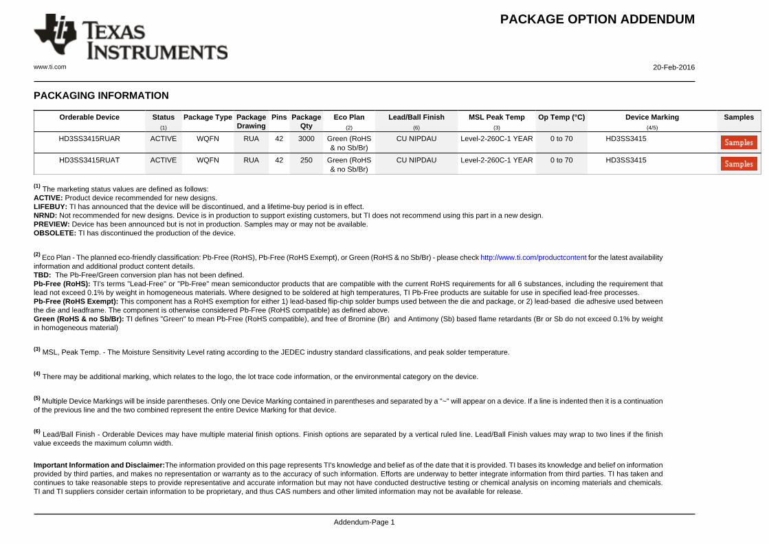
PACKAGING INFORMATION
Orderable Device Status(1)
Package Type PackageDrawing
Pins PackageQty
Eco Plan(2)
Lead/Ball Finish(6)
MSL Peak Temp(3)
Op Temp (°C) Device Marking(4/5)
Samples
HD3SS3415RUAR ACTIVE WQFN RUA 42 3000 Green (RoHS& no Sb/Br)
CU NIPDAU Level-2-260C-1 YEAR 0 to 70 HD3SS3415
HD3SS3415RUAT ACTIVE WQFN RUA 42 250 Green (RoHS& no Sb/Br)
CU NIPDAU Level-2-260C-1 YEAR 0 to 70 HD3SS3415
(1) The marketing status values are defined as follows:ACTIVE: Product device recommended for new designs.LIFEBUY: TI has announced that the device will be discontinued, and a lifetime-buy period is in effect.NRND: Not recommended for new designs. Device is in production to support existing customers, but TI does not recommend using this part in a new design.PREVIEW: Device has been announced but is not in production. Samples may or may not be available.OBSOLETE: TI has discontinued the production of the device.
(2) Eco Plan - The planned eco-friendly classification: Pb-Free (RoHS), Pb-Free (RoHS Exempt), or Green (RoHS & no Sb/Br) - please check http://www.ti.com/productcontent for the latest availabilityinformation and additional product content details.TBD: The Pb-Free/Green conversion plan has not been defined.Pb-Free (RoHS): TI's terms "Lead-Free" or "Pb-Free" mean semiconductor products that are compatible with the current RoHS requirements for all 6 substances, including the requirement thatlead not exceed 0.1% by weight in homogeneous materials. Where designed to be soldered at high temperatures, TI Pb-Free products are suitable for use in specified lead-free processes.Pb-Free (RoHS Exempt): This component has a RoHS exemption for either 1) lead-based flip-chip solder bumps used between the die and package, or 2) lead-based die adhesive used betweenthe die and leadframe. The component is otherwise considered Pb-Free (RoHS compatible) as defined above.Green (RoHS & no Sb/Br): TI defines "Green" to mean Pb-Free (RoHS compatible), and free of Bromine (Br) and Antimony (Sb) based flame retardants (Br or Sb do not exceed 0.1% by weightin homogeneous material)
(3) MSL, Peak Temp. - The Moisture Sensitivity Level rating according to the JEDEC industry standard classifications, and peak solder temperature.
(4) There may be additional marking, which relates to the logo, the lot trace code information, or the environmental category on the device.
(5) Multiple Device Markings will be inside parentheses. Only one Device Marking contained in parentheses and separated by a "~" will appear on a device. If a line is indented then it is a continuationof the previous line and the two combined represent the entire Device Marking for that device.
(6) Lead/Ball Finish - Orderable Devices may have multiple material finish options. Finish options are separated by a vertical ruled line. Lead/Ball Finish values may wrap to two lines if the finishvalue exceeds the maximum column width.
Important Information and Disclaimer:The information provided on this page represents TI's knowledge and belief as of the date that it is provided. TI bases its knowledge and belief on informationprovided by third parties, and makes no representation or warranty as to the accuracy of such information. Efforts are underway to better integrate information from third parties. TI has taken andcontinues to take reasonable steps to provide representative and accurate information but may not have conducted destructive testing or chemical analysis on incoming materials and chemicals.TI and TI suppliers consider certain information to be proprietary, and thus CAS numbers and other limited information may not be available for release.

PACKAGE OPTION ADDENDUM
www.ti.com 20-Feb-2016
Addendum-Page 2
In no event shall TI's liability arising out of such information exceed the total purchase price of the TI part(s) at issue in this document sold by TI to Customer on an annual basis.

TAPE AND REEL INFORMATION
*All dimensions are nominal
Device PackageType
PackageDrawing
Pins SPQ ReelDiameter
(mm)
ReelWidth
W1 (mm)
A0(mm)
B0(mm)
K0(mm)
P1(mm)
W(mm)
Pin1Quadrant
HD3SS3415RUAR WQFN RUA 42 3000 330.0 16.4 3.8 9.3 1.0 8.0 16.0 Q1
HD3SS3415RUAT WQFN RUA 42 250 180.0 16.4 3.8 9.3 1.0 8.0 16.0 Q1
PACKAGE MATERIALS INFORMATION
www.ti.com 24-Sep-2015
Pack Materials-Page 1

*All dimensions are nominal
Device Package Type Package Drawing Pins SPQ Length (mm) Width (mm) Height (mm)
HD3SS3415RUAR WQFN RUA 42 3000 367.0 367.0 38.0
HD3SS3415RUAT WQFN RUA 42 250 210.0 185.0 35.0
PACKAGE MATERIALS INFORMATION
www.ti.com 24-Sep-2015
Pack Materials-Page 2


IMPORTANT NOTICE
Texas Instruments Incorporated and its subsidiaries (TI) reserve the right to make corrections, enhancements, improvements and otherchanges to its semiconductor products and services per JESD46, latest issue, and to discontinue any product or service per JESD48, latestissue. Buyers should obtain the latest relevant information before placing orders and should verify that such information is current andcomplete. All semiconductor products (also referred to herein as “components”) are sold subject to TI’s terms and conditions of salesupplied at the time of order acknowledgment.TI warrants performance of its components to the specifications applicable at the time of sale, in accordance with the warranty in TI’s termsand conditions of sale of semiconductor products. Testing and other quality control techniques are used to the extent TI deems necessaryto support this warranty. Except where mandated by applicable law, testing of all parameters of each component is not necessarilyperformed.TI assumes no liability for applications assistance or the design of Buyers’ products. Buyers are responsible for their products andapplications using TI components. To minimize the risks associated with Buyers’ products and applications, Buyers should provideadequate design and operating safeguards.TI does not warrant or represent that any license, either express or implied, is granted under any patent right, copyright, mask work right, orother intellectual property right relating to any combination, machine, or process in which TI components or services are used. Informationpublished by TI regarding third-party products or services does not constitute a license to use such products or services or a warranty orendorsement thereof. Use of such information may require a license from a third party under the patents or other intellectual property of thethird party, or a license from TI under the patents or other intellectual property of TI.Reproduction of significant portions of TI information in TI data books or data sheets is permissible only if reproduction is without alterationand is accompanied by all associated warranties, conditions, limitations, and notices. TI is not responsible or liable for such altereddocumentation. Information of third parties may be subject to additional restrictions.Resale of TI components or services with statements different from or beyond the parameters stated by TI for that component or servicevoids all express and any implied warranties for the associated TI component or service and is an unfair and deceptive business practice.TI is not responsible or liable for any such statements.Buyer acknowledges and agrees that it is solely responsible for compliance with all legal, regulatory and safety-related requirementsconcerning its products, and any use of TI components in its applications, notwithstanding any applications-related information or supportthat may be provided by TI. Buyer represents and agrees that it has all the necessary expertise to create and implement safeguards whichanticipate dangerous consequences of failures, monitor failures and their consequences, lessen the likelihood of failures that might causeharm and take appropriate remedial actions. Buyer will fully indemnify TI and its representatives against any damages arising out of the useof any TI components in safety-critical applications.In some cases, TI components may be promoted specifically to facilitate safety-related applications. With such components, TI’s goal is tohelp enable customers to design and create their own end-product solutions that meet applicable functional safety standards andrequirements. Nonetheless, such components are subject to these terms.No TI components are authorized for use in FDA Class III (or similar life-critical medical equipment) unless authorized officers of the partieshave executed a special agreement specifically governing such use.Only those TI components which TI has specifically designated as military grade or “enhanced plastic” are designed and intended for use inmilitary/aerospace applications or environments. Buyer acknowledges and agrees that any military or aerospace use of TI componentswhich have not been so designated is solely at the Buyer's risk, and that Buyer is solely responsible for compliance with all legal andregulatory requirements in connection with such use.TI has specifically designated certain components as meeting ISO/TS16949 requirements, mainly for automotive use. In any case of use ofnon-designated products, TI will not be responsible for any failure to meet ISO/TS16949.
Products ApplicationsAudio www.ti.com/audio Automotive and Transportation www.ti.com/automotiveAmplifiers amplifier.ti.com Communications and Telecom www.ti.com/communicationsData Converters dataconverter.ti.com Computers and Peripherals www.ti.com/computersDLP® Products www.dlp.com Consumer Electronics www.ti.com/consumer-appsDSP dsp.ti.com Energy and Lighting www.ti.com/energyClocks and Timers www.ti.com/clocks Industrial www.ti.com/industrialInterface interface.ti.com Medical www.ti.com/medicalLogic logic.ti.com Security www.ti.com/securityPower Mgmt power.ti.com Space, Avionics and Defense www.ti.com/space-avionics-defenseMicrocontrollers microcontroller.ti.com Video and Imaging www.ti.com/videoRFID www.ti-rfid.comOMAP Applications Processors www.ti.com/omap TI E2E Community e2e.ti.comWireless Connectivity www.ti.com/wirelessconnectivity
Mailing Address: Texas Instruments, Post Office Box 655303, Dallas, Texas 75265Copyright © 2016, Texas Instruments Incorporated