ucc27531-q1 2.5-a and 5-a, 35-vmax vdd fet and igbt single ... · pdf file1 2 3 6 5 4 + en in...
TRANSCRIPT
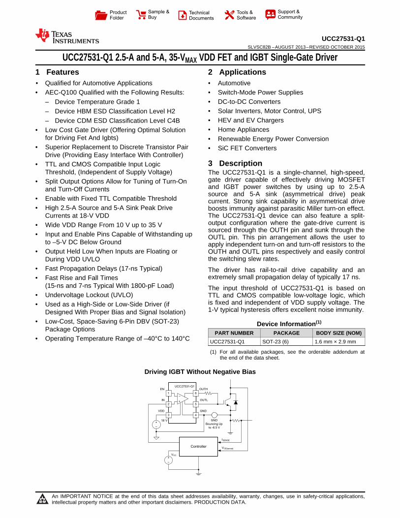
1
2
3
6
5
4
+
EN
IN
VDD
OUTH
OUTL
GND
+
–
18 V
UCC27531-Q1
Controller
+
–
VCC
GND
Bouncing Up
to -6.5 V
ISENSE
VCE(sense)
Product
Folder
Sample &Buy
Technical
Documents
Tools &
Software
Support &Community
UCC27531-Q1SLVSC82B –AUGUST 2013–REVISED OCTOBER 2015
UCC27531-Q1 2.5-A and 5-A, 35-VMAX VDD FET and IGBT Single-Gate Driver1 Features 2 Applications1• Qualified for Automotive Applications • Automotive• AEC-Q100 Qualified with the Following Results: • Switch-Mode Power Supplies
• DC-to-DC Converters– Device Temperature Grade 1• Solar Inverters, Motor Control, UPS– Device HBM ESD Classification Level H2• HEV and EV Chargers– Device CDM ESD Classification Level C4B• Home Appliances• Low Cost Gate Driver (Offering Optimal Solution
for Driving Fet And Igbts) • Renewable Energy Power Conversion• Superior Replacement to Discrete Transistor Pair • SiC FET Converters
Drive (Providing Easy Interface With Controller)3 Description• TTL and CMOS Compatible Input Logic
Threshold, (Independent of Supply Voltage) The UCC27531-Q1 is a single-channel, high-speed,gate driver capable of effectively driving MOSFET• Split Output Options Allow for Tuning of Turn-Onand IGBT power switches by using up to 2.5-Aand Turn-Off Currentssource and 5-A sink (asymmetrical drive) peak
• Enable with Fixed TTL Compatible Threshold current. Strong sink capability in asymmetrical drive• High 2.5-A Source and 5-A Sink Peak Drive boosts immunity against parasitic Miller turn-on effect.
The UCC27531-Q1 device can also feature a split-Currents at 18-V VDDoutput configuration where the gate-drive current is• Wide VDD Range From 10 V up to 35 Vsourced through the OUTH pin and sunk through the• Input and Enable Pins Capable of Withstanding up OUTL pin. This pin arrangement allows the user to
to –5-V DC Below Ground apply independent turn-on and turn-off resistors to the• Output Held Low When Inputs are Floating or OUTH and OUTL pins respectively and easily control
the switching slew rates.During VDD UVLO• Fast Propagation Delays (17-ns Typical) The driver has rail-to-rail drive capability and an
extremely small propagation delay of typically 17 ns.• Fast Rise and Fall Times(15-ns and 7-ns Typical With 1800-pF Load) The input threshold of UCC27531-Q1 is based on
• Undervoltage Lockout (UVLO) TTL and CMOS compatible low-voltage logic, whichis fixed and independent of VDD supply voltage. The• Used as a High-Side or Low-Side Driver (if1-V typical hysteresis offers excellent noise immunity.Designed With Proper Bias and Signal Isolation)
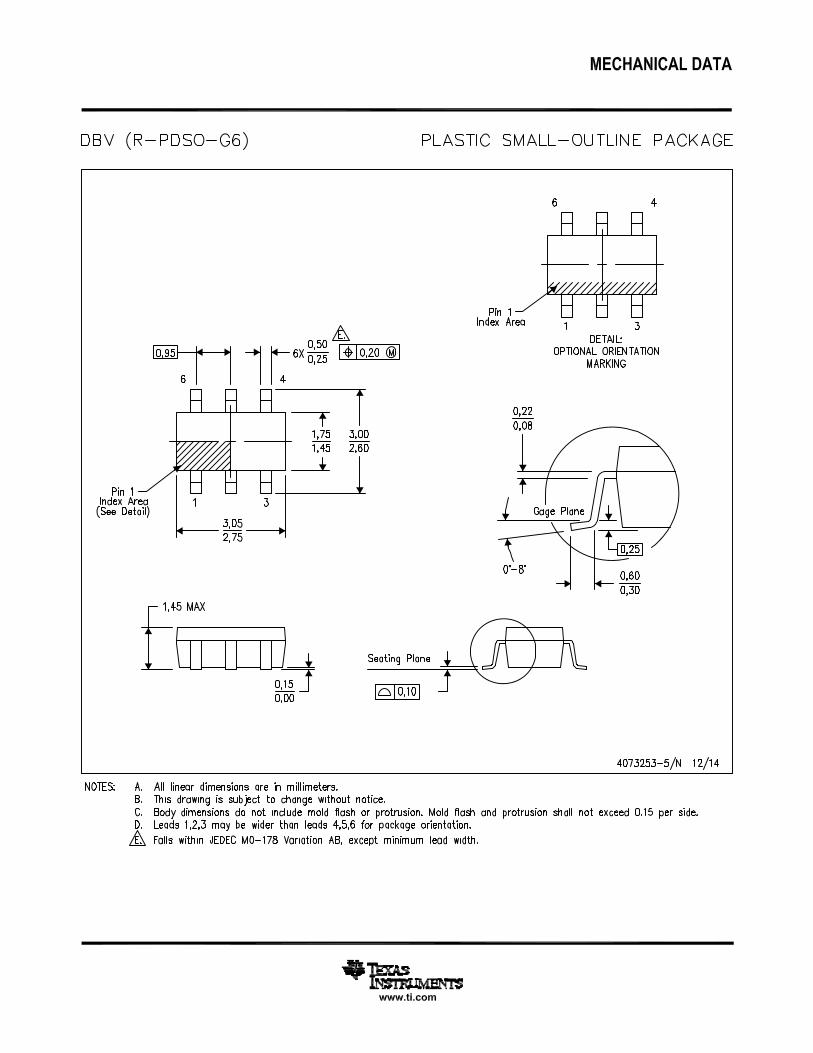
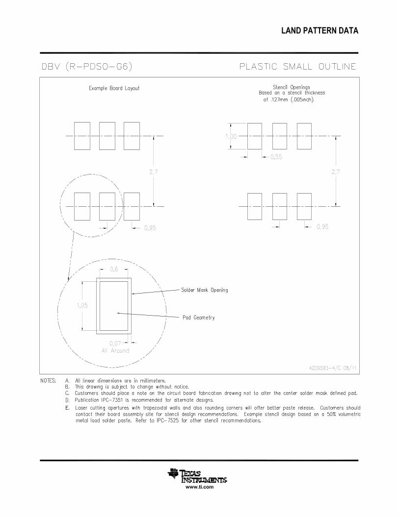
• Low-Cost, Space-Saving 6-Pin DBV (SOT-23) Device Information(1)Package Options PART NUMBER PACKAGE BODY SIZE (NOM)
• Operating Temperature Range of –40°C to 140°C UCC27531-Q1 SOT-23 (6) 1.6 mm × 2.9 mm
(1) For all available packages, see the orderable addendum atthe end of the data sheet.
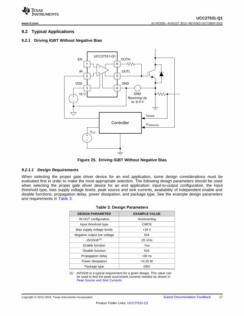
Driving IGBT Without Negative Bias
1
An IMPORTANT NOTICE at the end of this data sheet addresses availability, warranty, changes, use in safety-critical applications,intellectual property matters and other important disclaimers. PRODUCTION DATA.
UCC27531-Q1SLVSC82B –AUGUST 2013–REVISED OCTOBER 2015 www.ti.com
Table of Contents8.3 Feature Description................................................. 121 Features .................................................................. 18.4 Device Functional Modes........................................ 152 Applications ........................................................... 1
9 Application and Implementation ........................ 163 Description ............................................................. 19.1 Application Information............................................ 164 Revision History..................................................... 29.2 Typical Applications ................................................ 175 Description (continued)......................................... 3
10 Power Supply Recommendations ..................... 236 Pin Configuration and Functions ......................... 311 Layout................................................................... 237 Specifications......................................................... 4
11.1 Layout Guidelines ................................................. 237.1 Absolute Maximum Ratings ...................................... 411.2 Layout Example .................................................... 247.2 ESD Ratings.............................................................. 411.3 Thermal Considerations ........................................ 247.3 Recommended Operating Conditions....................... 4
12 Device and Documentation Support ................. 257.4 Thermal Information .................................................. 412.1 Community Resources.......................................... 257.5 Electrical Characteristics........................................... 512.2 Trademarks ........................................................... 257.6 Switching Characteristics .......................................... 512.3 Electrostatic Discharge Caution............................ 257.7 Typical Characteristics .............................................. 712.4 Glossary ................................................................ 258 Detailed Description ............................................ 11
13 Mechanical, Packaging, and Orderable8.1 Overview ................................................................. 11Information ........................................................... 258.2 Functional Block Diagram ....................................... 12
4 Revision HistoryNOTE: Page numbers for previous revisions may differ from page numbers in the current version.
Changes from Revision A (December 2013) to Revision B Page
• Added ESD Ratings table, Feature Description section, Device Functional Modes, Application and Implementationsection, Power Supply Recommendations section, Layout section, Device and Documentation Support section, andMechanical, Packaging, and Orderable Information section. ................................................................................................ 1
Changes from Original (August 2013) to Revision A Page
• Changed document from Product Preview to Production Data.............................................................................................. 1
2 Submit Documentation Feedback Copyright © 2013–2015, Texas Instruments Incorporated
Product Folder Links: UCC27531-Q1
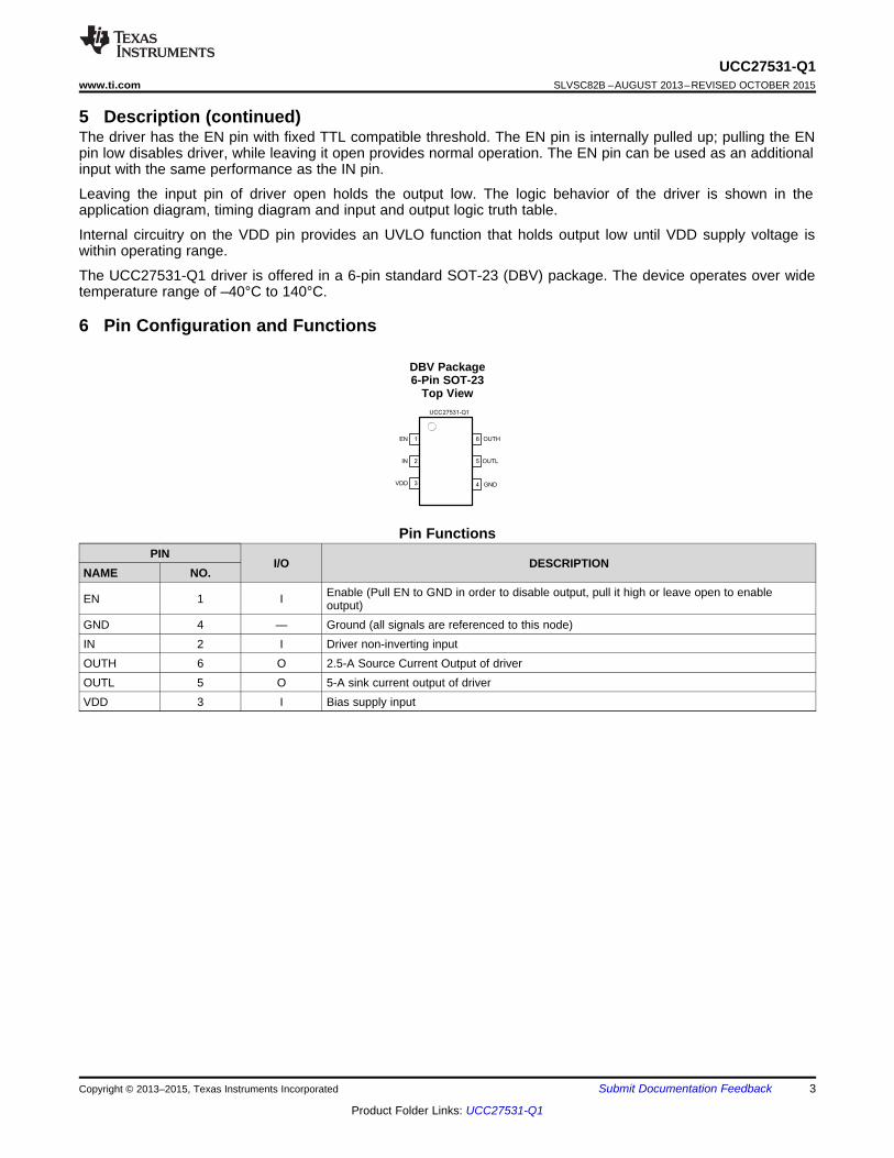
1
2
3
6
5
4
IN
EN
GND
OUTL
OUTH
VDD
UCC27531-Q1
UCC27531-Q1www.ti.com SLVSC82B –AUGUST 2013–REVISED OCTOBER 2015
5 Description (continued)The driver has the EN pin with fixed TTL compatible threshold. The EN pin is internally pulled up; pulling the ENpin low disables driver, while leaving it open provides normal operation. The EN pin can be used as an additionalinput with the same performance as the IN pin.
Leaving the input pin of driver open holds the output low. The logic behavior of the driver is shown in theapplication diagram, timing diagram and input and output logic truth table.
Internal circuitry on the VDD pin provides an UVLO function that holds output low until VDD supply voltage iswithin operating range.
The UCC27531-Q1 driver is offered in a 6-pin standard SOT-23 (DBV) package. The device operates over widetemperature range of –40°C to 140°C.
6 Pin Configuration and Functions
DBV Package6-Pin SOT-23
Top View
Pin FunctionsPIN
I/O DESCRIPTIONNAME NO.
Enable (Pull EN to GND in order to disable output, pull it high or leave open to enableEN 1 I output)GND 4 — Ground (all signals are referenced to this node)IN 2 I Driver non-inverting inputOUTH 6 O 2.5-A Source Current Output of driverOUTL 5 O 5-A sink current output of driverVDD 3 I Bias supply input
Copyright © 2013–2015, Texas Instruments Incorporated Submit Documentation Feedback 3
Product Folder Links: UCC27531-Q1
UCC27531-Q1SLVSC82B –AUGUST 2013–REVISED OCTOBER 2015 www.ti.com
7 Specifications
7.1 Absolute Maximum Ratings (1) (2) (3)
over operating free-air temperature range (unless otherwise noted)MIN MAX UNIT
Supply voltage VDD –0.3 35 VContinuous OUTH, OUTL, OUT –0.3 VDD + 0.3 VPulse OUTH, OUTL, OUT (200 ns) –2 VDD + 0.3 VContinuous IN, EN, IN+, IN-, IN1, IN2 –5 27 VPulse IN, EN, IN+, IN-, IN1, IN2 (1.5 µs) –6.5 27 VOperating virtual junction temperature, TJ –40 150 °C
Soldering, 10 sec. 300Lead temperature °C
Reflow 260Storage temperature, Tstg –65 150 °C
(1) Stresses beyond those listed under absolute maximum ratings may cause permanent damage to the device. These are stress ratingsonly and functional operation of the device at these or any other conditions beyond those indicated under recommended operatingconditions is not implied. Exposure to absolute-maximum-rated conditions for extended periods may affect device reliability.
(2) All voltages are with respect to GND unless otherwise noted. Currents are positive into, negative out of the specified terminal. SeePackaging Section of the datasheet for thermal limitations and considerations of packages.
(3) These devices are sensitive to electrostatic discharge; follow proper device handling procedures.
7.2 ESD RatingsVALUE UNIT
Human-body model (HBM), per ANSI/ESDA/JEDEC JS-001 (1) ±2000V(ESD) Electrostatic discharge VCharged-device model (CDM), per JEDEC specification JESD22- ±750C101 (2)
(1) JEDEC document JEP155 states that 500-V HBM allows safe manufacturing with a standard ESD control process.(2) JEDEC document JEP157 states that 250-V CDM allows safe manufacturing with a standard ESD control process.
7.3 Recommended Operating Conditionsover operating free-air temperature range (unless otherwise noted)
MIN NOM MAX UNITSupply voltage range, VDD 10 18 32 VAmbient temperature range –40 140 °CInput voltage, IN, IN+, IN-, IN1, IN2 –5 25 VEnable, EN –5 25 V
7.4 Thermal InformationUCC27531-Q1
THERMAL METRIC (1) DBV (SOT-23) UNIT6 PINS
RθJA Junction-to-ambient thermal resistance 178.3 °C/WRθJC(top) Junction-to-case (top) thermal resistance 109.7 °C/WRθJB Junction-to-board thermal resistance 28.3 °C/WψJT Junction-to-top characterization parameter 14.7 °C/WψJB Junction-to-board characterization parameter 27.8 °C/W
(1) For more information about traditional and new thermal metrics, see the Semiconductor and IC Package Thermal Metrics applicationreport, SPRA953.
4 Submit Documentation Feedback Copyright © 2013–2015, Texas Instruments Incorporated
Product Folder Links: UCC27531-Q1
UCC27531-Q1www.ti.com SLVSC82B –AUGUST 2013–REVISED OCTOBER 2015
7.5 Electrical CharacteristicsUnless otherwise noted, VDD = 18 V, TA = –40°C to 140°C, 1-µF capacitor from VDD to GND, f = 100 kHz. Currents arepositive into, negative out of the specified terminal. OUTH and OUTL are tied together for UCC27531-Q1. Typical conditionspecifications are at 25°C.
PARAMETER TEST CONDITIONS MIN TYP MAX UNITBIAS CURRENTS
VDD = 7, IN, EN = VDD 100 200 300IDDoff Startup current μA
IN, EN = GND 100 217 300UVLOVON Supply start threshold 8 8.9 9.8 V
Minimum operating voltageVOFF 7.3 8.2 9.1 Vafter supply startVDD_H Supply voltage hysteresis 0.7 VINPUT (IN)
Input signal high threshold,VIN_H Output High, EN = HIGH 1.8 2 2.2 Voutput highInput signal low threshold,VIN_L Output Low, EN = HIGH 0.8 1 1.2 Voutput low
VIN_HYS Input signal hysteresis 1 VENABLE (EN)VEN_H Enable signal high threshold Output High 1.7 1.9 2.1 VVEN_L Enable signal low threshold Output Low 0.8 1 1.2 VVEN_HYS Enable signal hysteresis 0.9 VOUTPUTS (OUTH/OUTL)
Source peak current (OUTH)/ISRC/SNK CLOAD = 0.22 µF, f = 1 kHz –2.5 / +5 Asink peak current (OUTL)VDD - VDD - VDD -VOH OUTH, high voltage IOUTH = –10 mA V0.2 0.12 0.07
VOL OUTL, low voltage IOUTL = 100 mA 0.065 0.125 VTA = 25°C, IOUT = –10 mA 11 12 12.5
ROH OUTH, pullup resistance ΩTA = –40°C to 140°C, IOUT = –10 mA 7 12 20TA = 25°C, IOUT = 100 mA 0.45 0.65 0.85
ROL OUTL, pulldown resistance ΩTA = –40°C to 140°C, IOUT = 100 mA 0.3 0.65 1.25
7.6 Switching CharacteristicsUnless otherwise noted, VDD = 18 V, TA = –40°C to 140°C, 1-µF capacitor from VDD to GND, f = 100 kHz. Currents arepositive into, negative out of the specified terminal. OUTH and OUTL are tied together for UCC27531-Q1. Typical conditionspecifications are at 25°C.
PARAMETER TEST CONDITIONS MIN TYP MAX UNITtR Rise time CLOAD = 1.8 nF 15 nstF Fall time CLOAD = 1.8 nF 7 nstD1 Turn-on propagation delay CLOAD = 1.8 nF, IN = 0 V to 5 V 17 26 nstD2 Turn-off propagation delay CLOAD = 1.8 nF, IN = 5 V to 0 V 17 26 ns
Copyright © 2013–2015, Texas Instruments Incorporated Submit Documentation Feedback 5
Product Folder Links: UCC27531-Q1
UCC27531-Q1SLVSC82B –AUGUST 2013–REVISED OCTOBER 2015 www.ti.com
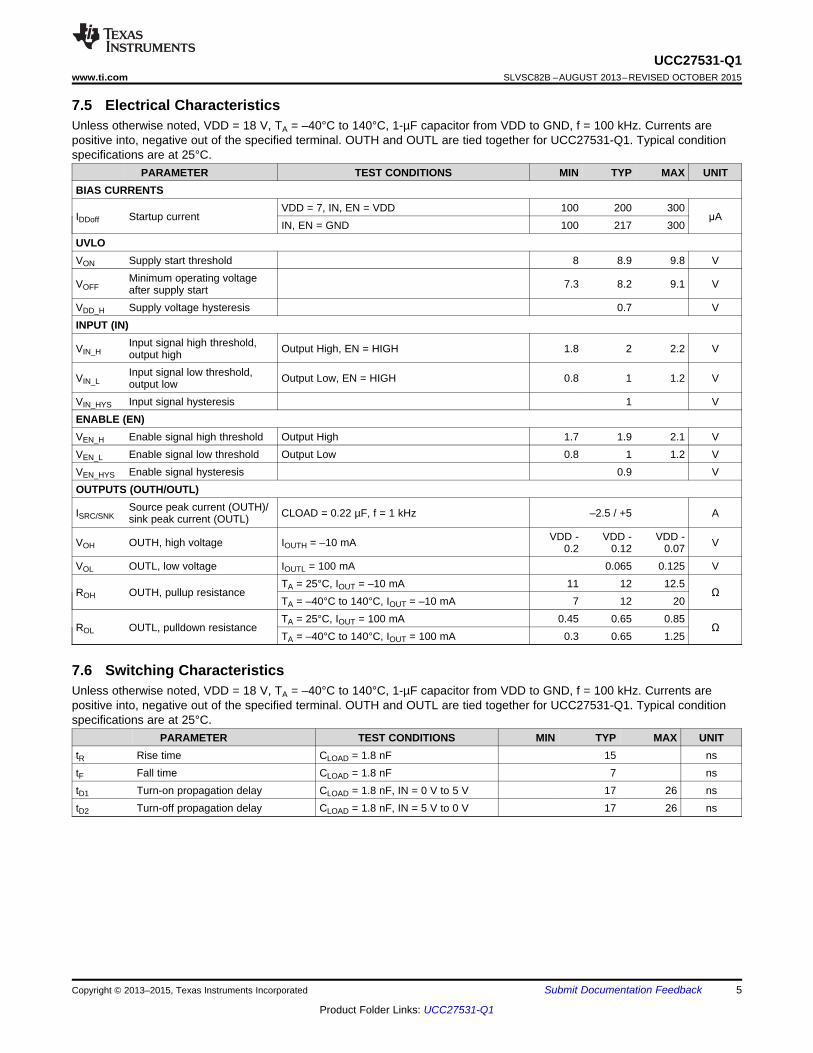
Figure 1. Timing Diagram (OUTPUT = OUTH tied to OUTL) INPUT = IN,(EN = VDD), or INPUT = EN, (IN = VDD)
6 Submit Documentation Feedback Copyright © 2013–2015, Texas Instruments Incorporated
Product Folder Links: UCC27531-Q1
0
5
10
15
20
25
30
0 100 200 300 400 500
Supply
Curr
ent
(mA
)
Frequency (kHz)
VDD = 10V
VDD = 18V
VDD = 32V
C001
100
150
200
250
300
-50 0 50 100 150
Sta
rtu
pC
urr
en
t(µ
A)
Temperature ( °C)
EN=IN=Vdd
EN=IN=GND
C005
15
17
19
21
23
25
27
0 10 20 30 40
IN-
Inpu
t T
o O
utpu
t P
ropa
gatio
n D
elay
(ns
)
Supply Voltage (V)
OUT RISING, IN- 5V to0VOUT FALLING, IN- 0Vto 5V
C001
15
17
19
21
0 10 20 30 40
Input
To
Outp
ut
Pro
pagation
Dela
y(n
s)
Supply Voltage (V)
Turn-On
Turn-Off
C003
5
10
15
20
25
0 10 20 30 40
Ris
eT
ime
(ns)
Supply Voltage (V) C001
2
4
6
8
10
12
0 10 20 30 40
Fall
Tim
e(n
s)
Supply Voltage (V) C002
UCC27531-Q1www.ti.com SLVSC82B –AUGUST 2013–REVISED OCTOBER 2015
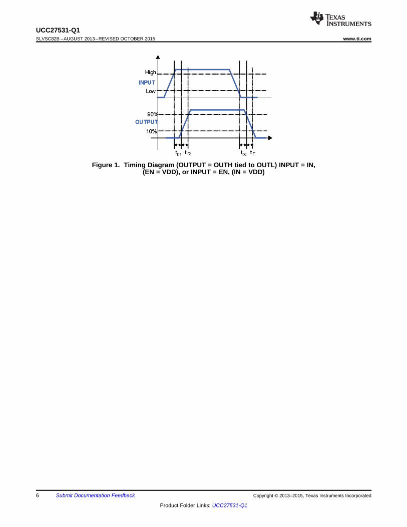
7.7 Typical CharacteristicsIf not specified, INPUT refers to non-inverting input
Figure 2. Rise Time vs Supply Voltage Figure 3. Fall Time vs Supply Voltage
Figure 5. IN - Propagation Delay vs SupplyFigure 4. Propagation Delay vs Supply Voltage
Figure 7. Start-Up Current vs TemperatureFigure 6. Operating Supply Current vs Frequency
Copyright © 2013–2015, Texas Instruments Incorporated Submit Documentation Feedback 7
Product Folder Links: UCC27531-Q1
5
10
15
20
25
-50 0 50 100 150
Outp
ut
Pu
ll-U
pR
esis
tance
()
Ω
Temperature ( °C)
ROH
C010
0.2
0.4
0.6
0.8
1
1.2
-50 0 50 100 150
Outp
ut
Pu
ll-D
ow
nR
esis
tance
()
Ω
Temperature ( °C)
ROL
C011
0.8
1
1.2
1.4
1.6
1.8
2
2.2
2.4
-50 0 50 100 150
Inpu
t T
hres
hold
(V
)
7HPSHUDWXUHÛ&
Turn-On
Turn-Off
C008
0.8
1
1.2
1.4
1.6
1.8
2
2.2
2.4
-50 0 50 100 150
Ena
ble
Thr
esho
ld (
V)
7HPSHUDWXUHÛ&
Enable
Disable
C009
8
8.4
8.8
9.2
9.6
-50 0 50 100 150
Vdd
UV
LO T
hres
hold
(V
)
7HPSHUDWXUHÛ&
UVLO Rising
UVLO Falling
C007
3.5
3.7
3.9
4.1
4.3
4.5
-50 0 50 100 150
Idd
(mA
)
Temperature ( °C)
C006
UCC27531-Q1SLVSC82B –AUGUST 2013–REVISED OCTOBER 2015 www.ti.com
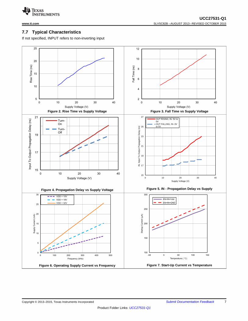
Typical Characteristics (continued)If not specified, INPUT refers to non-inverting input
Figure 8. Operating Supply Current vs Temperature (Output Figure 9. UVLO Threshold Voltage vs TemperatureSwitching)
Figure 10. Input Threshold vs Temperature Figure 11. Enable Threshold vs Temperature
Figure 12. Output Pullup Resistance vs Temperature Figure 13. Output Pulldown Resistance vs Temperature
8 Submit Documentation Feedback Copyright © 2013–2015, Texas Instruments Incorporated
Product Folder Links: UCC27531-Q1
4
5
6
7
8
9
-50 0 50 100 150
Fall
Tim
e(n
s)
Temperature ( °C)
C015
0
2
4
6
8
10
0 10 20 30 40
Su
pply
Cu
rren
t(m
A)
Supply Voltage (V)
C016
10
14
18
22
26
30
-50 0 50 100 150
IN-
Pro
pagation
Dela
y(n
s)
Temperature ( °C)
OUT RISING, IN- 5V to 0V
OUT FALLING, IN- 0V to 5V
C003
11
12
13
14
15
16
-50 0 50 100 150
Ris
eT
ime
(ns)
Temperature ( °C)
C014
0.2
0.3
0.4
0.5
0.6
-50 0 50 100 150
Opera
ting
Supply
Curr
ent
(mA
)
Temperature ( °C)
IN=HIGH
IN=LOW
C012
10
15
20
25
30
-50 0 50 100 150
Pro
pagation
Dela
y(n
s)
Temperature ( °C)
Turn-On
Turn-Off
C013
UCC27531-Q1www.ti.com SLVSC82B –AUGUST 2013–REVISED OCTOBER 2015
Typical Characteristics (continued)If not specified, INPUT refers to non-inverting input
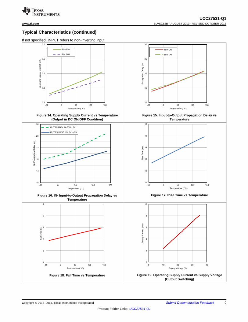
Figure 14. Operating Supply Current vs Temperature Figure 15. Input-to-Output Propagation Delay vs(Output in DC ON/OFF Condition) Temperature
Figure 17. Rise Time vs TemperatureFigure 16. IN- Input-to-Output Propagation Delay vsTemperature
Figure 19. Operating Supply Current vs Supply VoltageFigure 18. Fall Time vs Temperature(Output Switching)
Copyright © 2013–2015, Texas Instruments Incorporated Submit Documentation Feedback 9
Product Folder Links: UCC27531-Q1
10
20
30
40
50
60
70
0 10 20 30 40
Fa
llT
ime
(ns)
Supply Voltage (V)
C018
40
60
80
100
120
140
0 10 20 30 40
Ris
e T
ime
(ns)
Supply Voltage (V) C017
Cload = 10nF
UCC27531-Q1SLVSC82B –AUGUST 2013–REVISED OCTOBER 2015 www.ti.com
Typical Characteristics (continued)If not specified, INPUT refers to non-inverting input
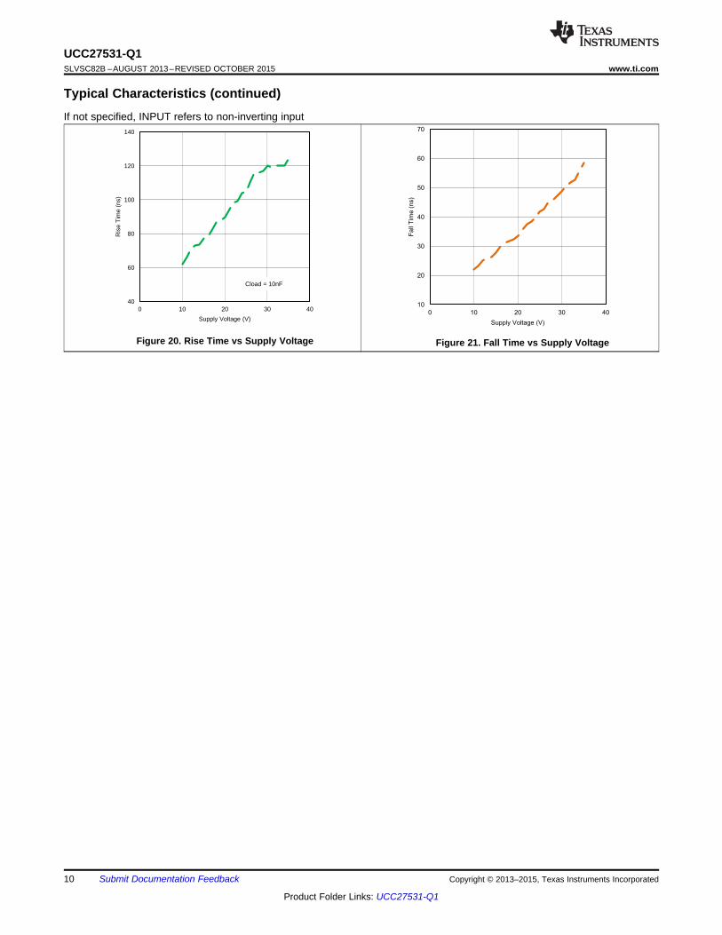
Figure 20. Rise Time vs Supply Voltage Figure 21. Fall Time vs Supply Voltage
10 Submit Documentation Feedback Copyright © 2013–2015, Texas Instruments Incorporated
Product Folder Links: UCC27531-Q1
UCC27531-Q1www.ti.com SLVSC82B –AUGUST 2013–REVISED OCTOBER 2015
8 Detailed Description
8.1 OverviewThe UCC27531-Q1 is a single-channel, high-speed, gate driver capable of effectively driving MOSFET and IGBTpower switches by up to 2.5-A source and 5-A sink (asymmetrical drive) peak current. Strong sink capability inasymmetrical drive boosts immunity against parasitic Miller turn-on effect. The UCC27531-Q1 device can alsofeature a split-output configuration where the gate-drive current is sourced through the OUTH pin and sunkthrough the OUTL pin. This pin arrangement allows the user to apply independent turn-on and turn-off resistorsto the OUTH and OUTL pins, respectively, and easily control the switching slew rates.
The driver has rail-to-rail drive capability and extremely small propagation delay, typically 17 ns.
The input threshold of UCC27531-Q1 is based on TTL and CMOS compatible low-voltage logic, which is fixedand independent of VDD supply voltage. The 1-V typical hysteresis offers excellent noise immunity.
The driver has an EN pin with fixed TTL compatible threshold. EN is internally pulled up; pulling EN low disablesthe driver, while leaving EN open provides normal operation. The EN pin can be used as an additional input withthe same performance as the IN, IN+, IN1, and IN2 pins.
Table 1. UCC27531-Q1 Features and BenefitsFEATURE BENEFIT
High source and sink current capability, 2.5 A High current capability offers flexibility in employing UCC27531-Q1 device to drive a varietyand 5 A (asymmetrical). of power switching devices at varying speeds.Low 17 ns (typ) propagation delay. Extremely low pulse transmission distortion.Wide VDD operating range of 10 V to 32 V. Flexibility in system design.
Can be used in split-rail systems such as driving IGBTs with both positive andnegative(relative to Emitter) supplies.Optimal for many SiC FETs.
VDD UVLO protection. Outputs are held Low in UVLO condition, which ensures predictable, glitch-free operation atpower up and power down.High UVLO of 8.9 V typical ensures that power switch is not on in high-impedance statewhich could result in high power dissipation or even failures.
Outputs held low when input pin (INx) in Safety feature, especially useful in passing abnormal condition tests during safetyfloating condition. certificationSplit output structure option (OUTH, OUTL). Allows independent optimization of turn-on and turn-off speeds using series gate resistors.Strong sink current (5 A) and low pull-down High immunity to high dV/dt Miller turn-on events.impedance (0.65 Ω).CMOS and TTL compatible input threshold Enhanced noise immunity, while retaining compatibility with microcontroller logic level inputlogic with wide hysteresis. signals (3.3 V, 5 V) optimized for digital power.Input capable of withstanding –6.5 V. Enhanced signal reliability in noisy environments that experience ground bounce on the
gate driver.
Copyright © 2013–2015, Texas Instruments Incorporated Submit Documentation Feedback 11
Product Folder Links: UCC27531-Q1
OUT
IN
VDD
VDD Threshold
2
1
4
3
6
5
VREF
UVLO
VDD
VDD
VDD
OUTH
OUTL
IN
EN
GND
UCC27531-Q1SLVSC82B –AUGUST 2013–REVISED OCTOBER 2015 www.ti.com
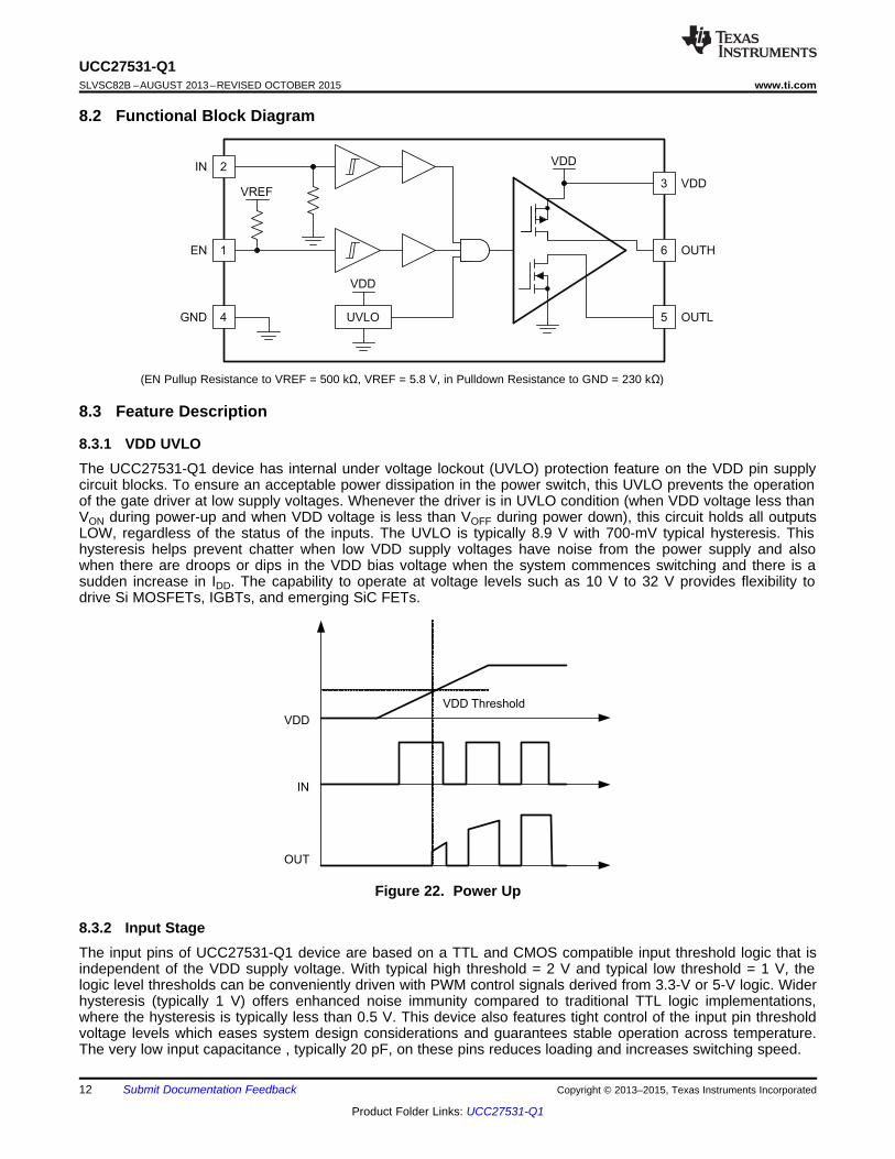
8.2 Functional Block Diagram
(EN Pullup Resistance to VREF = 500 kΩ, VREF = 5.8 V, in Pulldown Resistance to GND = 230 kΩ)
8.3 Feature Description
8.3.1 VDD UVLOThe UCC27531-Q1 device has internal under voltage lockout (UVLO) protection feature on the VDD pin supplycircuit blocks. To ensure an acceptable power dissipation in the power switch, this UVLO prevents the operationof the gate driver at low supply voltages. Whenever the driver is in UVLO condition (when VDD voltage less thanVON during power-up and when VDD voltage is less than VOFF during power down), this circuit holds all outputsLOW, regardless of the status of the inputs. The UVLO is typically 8.9 V with 700-mV typical hysteresis. Thishysteresis helps prevent chatter when low VDD supply voltages have noise from the power supply and alsowhen there are droops or dips in the VDD bias voltage when the system commences switching and there is asudden increase in IDD. The capability to operate at voltage levels such as 10 V to 32 V provides flexibility todrive Si MOSFETs, IGBTs, and emerging SiC FETs.
Figure 22. Power Up
8.3.2 Input StageThe input pins of UCC27531-Q1 device are based on a TTL and CMOS compatible input threshold logic that isindependent of the VDD supply voltage. With typical high threshold = 2 V and typical low threshold = 1 V, thelogic level thresholds can be conveniently driven with PWM control signals derived from 3.3-V or 5-V logic. Widerhysteresis (typically 1 V) offers enhanced noise immunity compared to traditional TTL logic implementations,where the hysteresis is typically less than 0.5 V. This device also features tight control of the input pin thresholdvoltage levels which eases system design considerations and guarantees stable operation across temperature.The very low input capacitance , typically 20 pF, on these pins reduces loading and increases switching speed.
12 Submit Documentation Feedback Copyright © 2013–2015, Texas Instruments Incorporated
Product Folder Links: UCC27531-Q1
VDD
R
R
RNMOS ,Pull Up
VDD
ROH
ROL
Narrow Pulse at
each Turn On
OUTH
Input SignalAnti Shoot-
Through
CircuitryOUTL
UCC27531-Q1www.ti.com SLVSC82B –AUGUST 2013–REVISED OCTOBER 2015
Feature Description (continued)The device features an important safety function wherein, whenever the input pin is in a floating condition, theoutput is held in the low state. This is achieved using pullup or pulldown resistors on the input pins as shown inthe block diagrams.
The input stage of the driver should preferably be driven by a signal with a short rise or fall time. Caution must beexercised whenever the driver is used with slowly varying input signals, especially in situations where the deviceis located in a separate daughter board or PCB layout has long input connection traces:• High dI/dt current from the driver output coupled with board layout parasitics can cause ground bounce. Since
the device features just one GND pin which may be referenced to the power ground, this may interfere withthe differential voltage between Input pins and GND and trigger an unintended change of output state.Because of fast 17 ns propagation delay, this can ultimately result in high-frequency oscillations, whichincreases power dissipation and poses risk of damage
• 1-V Input threshold hysteresis boosts noise immunity compared to most other industry standard drivers.
If limiting the rise or fall times to the power device to reduce EMI is necessary, then an external resistance ishighly recommended between the output of the driver and the power device instead of adding delays on the inputsignal. This external resistor has the additional benefit of reducing part of the gate charge related powerdissipation in the gate driver device package and transferring it into the external resistor itself.
Finally, because of the unique input structure that allows negative voltage capability on the Input and Enablepins, caution must be used in the following applications:• Input or Enable pins are switching to amplitude > 15 V• Input or Enable pins are switched at dV/dt > 2 V/nsIf both of these conditions occur, it is advised to add a series 150-Ω resistor for the pin(s) being switched to limitthe current through the input structure.
8.3.3 Enable FunctionThe Enable (EN) pin of the UCC27531-Q1 has an internal pullup resistor to an internal reference voltage soleaving Enable floating turns on the driver and allows it to send output signals properly. If desired, the Enable canalso be driven by low-voltage logic to enable and disable the driver.
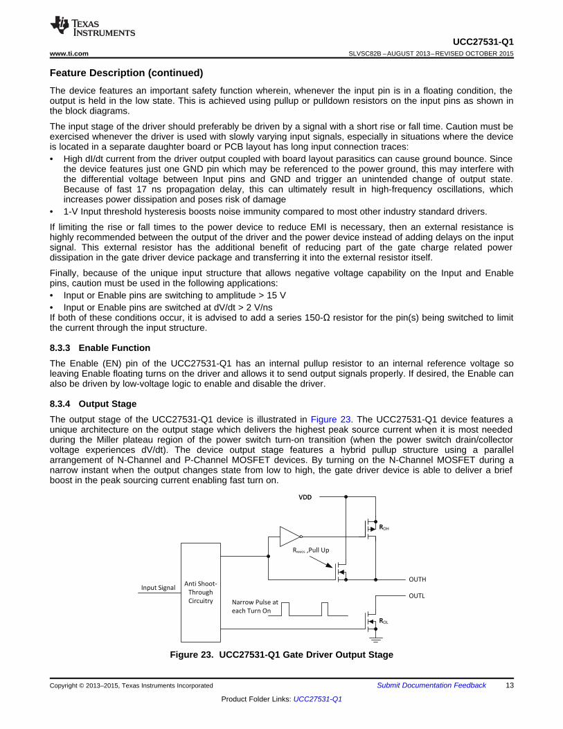
8.3.4 Output StageThe output stage of the UCC27531-Q1 device is illustrated in Figure 23. The UCC27531-Q1 device features aunique architecture on the output stage which delivers the highest peak source current when it is most neededduring the Miller plateau region of the power switch turn-on transition (when the power switch drain/collectorvoltage experiences dV/dt). The device output stage features a hybrid pullup structure using a parallelarrangement of N-Channel and P-Channel MOSFET devices. By turning on the N-Channel MOSFET during anarrow instant when the output changes state from low to high, the gate driver device is able to deliver a briefboost in the peak sourcing current enabling fast turn on.
Figure 23. UCC27531-Q1 Gate Driver Output Stage
Copyright © 2013–2015, Texas Instruments Incorporated Submit Documentation Feedback 13
Product Folder Links: UCC27531-Q1
Gate Driver
ROL
RG
CGD
CGS
COSS
VDS VIN
ISNK VIN
VTH
ON OFF
Miller Turn -On Spike in V GS
VDS of
MOSFET
VGS of
MOSFET
UCC27531-Q1SLVSC82B –AUGUST 2013–REVISED OCTOBER 2015 www.ti.com
Feature Description (continued)Split output depicted in Figure 23. For devices with single OUT pin, OUTH and OUTL are connected internallyand then connected to OUT.
The ROH parameter (see Electrical Characteristics) is a DC measurement and it is representative of the on-resistance of the P-Channel device only, because the N-Channel device is turned-on only during output changeof state from low to high. Thus the effective resistance of the hybrid pullup stage is much lower than what isrepresented by ROH parameter. The pulldown structure is composed of a N-Channel MOSFET only. The ROLparameter (see Electrical Characteristics), which is also a DC measurement, is representative of true impedanceof the pulldown stage in the device. In UCC27531-Q1, the effective resistance of the hybrid pullup structure isapproximately 3 x ROL.
The UCC27531-Q1 is capable of delivering 2.5-A source, and up to 5-A sink at VDD = 18 V. Strong sinkcapability results in a very low pulldown impedance in the driver output stage which boosts immunity against theparasitic Miller turn-on (high slew rate dV/dt turn on) effect that is seen in both IGBT and FET power switches .
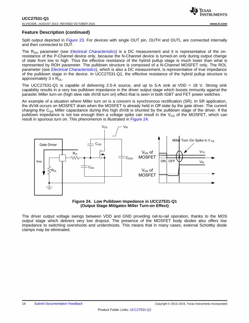
An example of a situation where Miller turn on is a concern is synchronous rectification (SR). In SR application,the dV/dt occurs on MOSFET drain when the MOSFET is already held in Off state by the gate driver. The currentcharging the CGD Miller capacitance during this high dV/dt is shunted by the pulldown stage of the driver. If thepulldown impedance is not low enough then a voltage spike can result in the VGS of the MOSFET, which canresult in spurious turn on. This phenomenon is illustrated in Figure 24.
Figure 24. Low Pulldown Impedance in UCC27531-Q1(Output Stage Mitigates Miller Turn-on Effect)
The driver output voltage swings between VDD and GND providing rail-to-rail operation, thanks to the MOSoutput stage which delivers very low dropout. The presence of the MOSFET body diodes also offers lowimpedance to switching overshoots and undershoots. This means that in many cases, external Schottky diodeclamps may be eliminated.
14 Submit Documentation Feedback Copyright © 2013–2015, Texas Instruments Incorporated
Product Folder Links: UCC27531-Q1
UCC27531-Q1www.ti.com SLVSC82B –AUGUST 2013–REVISED OCTOBER 2015
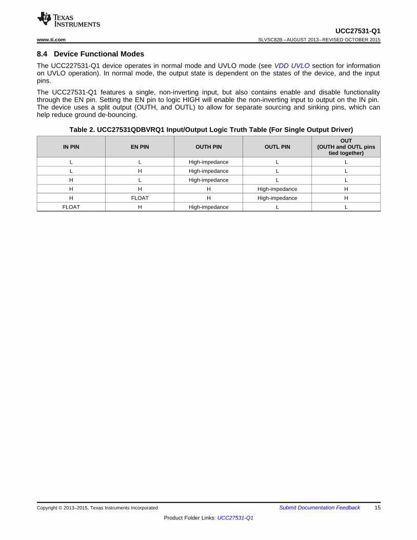
8.4 Device Functional ModesThe UCC227531-Q1 device operates in normal mode and UVLO mode (see VDD UVLO section for informationon UVLO operation). In normal mode, the output state is dependent on the states of the device, and the inputpins.
The UCC27531-Q1 features a single, non-inverting input, but also contains enable and disable functionalitythrough the EN pin. Setting the EN pin to logic HIGH will enable the non-inverting input to output on the IN pin.The device uses a split output (OUTH, and OUTL) to allow for separate sourcing and sinking pins, which canhelp reduce ground de-bouncing.
Table 2. UCC27531QDBVRQ1 Input/Output Logic Truth Table (For Single Output Driver)OUT
IN PIN EN PIN OUTH PIN OUTL PIN (OUTH and OUTL pinstied together)
L L High-impedance L LL H High-impedance L LH L High-impedance L LH H H High-impedance HH FLOAT H High-impedance H
FLOAT H High-impedance L L
Copyright © 2013–2015, Texas Instruments Incorporated Submit Documentation Feedback 15
Product Folder Links: UCC27531-Q1
UCC27531-Q1SLVSC82B –AUGUST 2013–REVISED OCTOBER 2015 www.ti.com
9 Application and Implementation
NOTEInformation in the following applications sections is not part of the TI componentspecification, and TI does not warrant its accuracy or completeness. TI’s customers areresponsible for determining suitability of components for their purposes. Customers shouldvalidate and test their design implementation to confirm system functionality.
9.1 Application InformationHigh-current gate driver devices are required in switching power applications for a variety of reasons. In order toenable fast switching of power devices and reduce associated switching power losses, a powerful gate driver canbe employed between the PWM output of controllers or signal isolation devices and the gates of the powersemiconductor devices. Further, gate drivers are indispensable when sometimes it is just not feasible to have thePWM controller directly drive the gates of the switching devices. The situation is encountered often because thePWM signal from a digital controller or signal isolation device is often a 3.3-V or 5-V logic signal which is notcapable of effectively turning on a power switch. A level shifting circuitry is needed to boost the logic-level signalto the gate-drive voltage in order to fully turn on the power device and minimize conduction losses. Traditionalbuffer drive circuits based on NPN/PNP bipolar, (or p- n-channel MOSFET), transistors in totem-polearrangement, being emitter follower configurations, prove inadequate for this because they lack level-shiftingcapability and low-drive voltage protection. Gate drivers effectively combine both the level-shifting, buffer driveand UVLO functions. Gate drivers also find other needs such as minimizing the effect of switching noise bylocating the high-current driver physically close to the power switch, driving gate-drive transformers andcontrolling floating power device gates, reducing power dissipation and thermal stress in controllers by movinggate charge power losses into itself.
The UCC27531-Q1 is very flexible in this role with a strong current drive capability and wide supply voltagerange up to 32 V. This allows the driver to be used in 12-V Si MOSFET applications, 20-V and –5-V (relative toSource) SiC FET applications, 15-V and –15-V(relative to Emitter) IGBT applications and many others. As asingle-channel driver, the UCC27531-Q1 can be used as a low-side or high-side driver. To use as a low-sidedriver, the switch ground is usually the system ground so it can be connected directly to the gate driver. To useas a high-side driver with a floating return node however, signal isolation is needed from the controller as well asan isolated bias to the UCC27531-Q1. Alternatively, in a high-side drive configuration the UCC27531-Q1 can betied directly to the controller signal and biased with a non-isolated supply. However, in this configuration theoutputs of the UCC27531-Q1 need to drive a pulse transformer which then drives the power-switch to workproperly with the floating source and emitter of the power switch. Further, having the ability to control turn-on andturn-off speeds independently with both the OUTH and OUTL pins ensures optimum efficiency while maintainingsystem reliability. These requirements coupled with the need for low propagation delays and availability incompact, low-inductance packages with good thermal capability makes gate driver devices such as theUCC27531-Q1 extremely important components in switching power combining benefits of high-performance, lowcost, component count and board space reduction and simplified system design.
16 Submit Documentation Feedback Copyright © 2013–2015, Texas Instruments Incorporated
Product Folder Links: UCC27531-Q1
1
2
3
6
5
4
+
EN
IN
VDD
OUTH
OUTL
GND
+
–
18 V
UCC27531-Q1
Controller
+
–
VCC
GND
Bouncing Up
to -6.5 V
ISENSE
VCE(sense)
UCC27531-Q1www.ti.com SLVSC82B –AUGUST 2013–REVISED OCTOBER 2015
9.2 Typical Applications
9.2.1 Driving IGBT Without Negative Bias
Figure 25. Driving IGBT Without Negative Bias
9.2.1.1 Design RequirementsWhen selecting the proper gate driver device for an end application, some design considerations must beevaluated first in order to make the most appropriate selection. The following design parameters should be usedwhen selecting the proper gate driver device for an end application: input-to-output configuration, the inputthreshold type, bias supply voltage levels, peak source and sink currents, availability of independent enable anddisable functions, propagation delay, power dissipation, and package type. See the example design parametersand requirements in Table 3.
Table 3. Design ParametersDESIGN PARAMETER EXAMPLE VALUEIN-OUT configuration NoninvertingInput threshold type CMOS
Bias supply voltage levels +18 VNegative output low voltage N/A
dVDS/dt (1) 20 V/nsEnable function YesDisable function N/A
Propagation delay <30 nsPower dissipation <0.25 W
Package type DBV
(1) dVDS/dt is a typical requirement for a given design. This value canbe used to find the peak source/sink currents needed as shown inPeak Source and Sink Currents.
Copyright © 2013–2015, Texas Instruments Incorporated Submit Documentation Feedback 17
Product Folder Links: UCC27531-Q1
UCC27531-Q1SLVSC82B –AUGUST 2013–REVISED OCTOBER 2015 www.ti.com
9.2.1.2 Detailed Design Procedure
9.2.1.2.1 Input-to-Output Configuration
See the Device Functional Modes section for information on individual device functionality.
9.2.1.2.2 Input Threshold Type
The type of Input voltage threshold determines the type of controller that can be used with the gate driver device.The UCC27531-Q1 device features a TTL and CMOS-compatible input threshold logic, with wide hysteresis. Thethreshold voltage levels are low voltage and independent of the VDD supply voltage, which allows compatibilitywith both logic-level input signals from microcontrollers as well as higher-voltage input signals from analogcontrollers. See the Electrical Characteristics table for the actual input threshold voltage levels and hysteresisspecifications for the UCC227531-Q1 device.
9.2.1.2.3 VDD Bias Supply Voltage
The bias supply voltage to be applied to the VDD pin of the device should never exceed the values listed in theRecommended Operating Conditions table. However, different power switches demand different voltage levels tobe applied at the gate terminals for effective turnon and turnoff. With certain power switches, a positive gatevoltage may be required for turnon and a negative gate voltage may be required for turnoff, in which case theVDD bias supply equals the voltage differential. With an operating range from 10 V to 32 V, the UCC227531-Q1device can be used to drive a power switches such as power MOSFETS and IGBTs (VGE = 15 V, 18 V).
9.2.1.2.4 Peak Source and Sink Currents
Generally, the switching speed of the power switch during turnon and turnoff should be as fast as possible tominimize switching power losses. The gate driver device must be able to provide the required peak current forachieving the targeted switching speeds for the targeted power MOSFET.
Using the example of a power MOSFET, the system requirement for the switching speed is typically described interms of the slew rate of the drain-to-source voltage of the power MOSFET (such as dVDS/dt). For example, thesystem requirement might state that a SPP20N60C3 power MOSFET must be turned on with a dVDS/dt of 20V/ns or higher under a DC bus voltage of 400 V in a continuous-conduction-mode (CCM) boost PFC-converterapplication. This type of application is an inductive hard-switching application and reducing switching powerlosses is critical. This requirement means that the entire drain-to-source voltage swing during power MOSFETturn-on event (from 400 V in the OFF state to VDS(on) in on state) must be completed in approximately 20 ns orless. When the drain-to-source voltage swing occurs, the Miller charge of the power MOSFET (QGD parameterin SPP20N60C3 power MOSFET data sheet = 33 nC typical) is supplied by the peak current of gate driver.According to power MOSFET inductive switching mechanism, the gate-to-source voltage of the power MOSFETat this time is the Miller plateau voltage, which is typically a few volts higher than the threshold voltage of thepower MOSFET, VGS(TH).
To achieve the targeted dVDS/dt, the gate driver must be capable of providing the QGD charge in 20 ns or less.In other words a peak current of 1.65 A (= 33 nC / 20 ns) or higher must be provided by the gate driver. TheUCC27531-Q1 series of gate drivers can provide 2.5-A peak sourcing current, and 5A peak sinking current whichclearly exceeds the design requirement and has the capability to meet the switching speed needed. The 1.5xsourcing, and 3x sinking overdrive capability provides an extra margin against part-to-part variations in the QGDparameter of the power MOSFET along with additional flexibility to insert external gate resistors and fine tune theswitching speed for efficiency versus EMI optimizations. However, in practical designs the parasitic traceinductance in the gate drive circuit of the PCB will have a definitive role to play on the power MOSFET switchingspeed. The effect of this trace inductance is to limit the dI/dt of the output current pulse of the gate driver. Toillustrate this, consider output current pulse waveform from the gate driver to be approximated to a triangularprofile, where the area under the triangle (½ ×IPEAK × time) would equal the total gate charge of the powerMOSFET (QG parameter in SPP20N60C3 power MOSFET datasheet = 87 nC typical). If the parasitic traceinductance limits the dI/dt then a situation may occur in which the full peak current capability of the gate driver isnot fully achieved in the time required to deliver the QG required for the power MOSFET switching. In otherwords, the time parameter in the equation would dominate and the IPEAK value of the current pulse would bemuch less than the true peak current capability of the device, while the required QG is still delivered. Because ofthis, the desired switching speed may not be realized, even when theoretical calculations indicate the gate drivercan achieve the targeted switching speed. Thus, placing the gate driver device very close to the power MOSFETand designing a tight gate drive-loop with minimal PCB trace inductance is important to realize the full peak-current capability of the gate driver.
18 Submit Documentation Feedback Copyright © 2013–2015, Texas Instruments Incorporated
Product Folder Links: UCC27531-Q1
2G LOAD DD sw g DD swP C V f Q V f= =
2G LOAD DD swP C V f=
2G LOAD DD
1E C V
2=
DISS DC SWP P P= +
UCC27531-Q1www.ti.com SLVSC82B –AUGUST 2013–REVISED OCTOBER 2015
9.2.1.2.5 Enable and Disable Function
Certain applications demand independent control of the output state of the driver without involving the inputsignal. A pin which offers an enable and disable function achieves this requirement. For these applications, theUCC27531-Q1 is suitable as it features an input pin and an Enable pin.
9.2.1.2.6 Propagation Delay
The acceptable propagation delay from the gate driver is dependent on the switching frequency at which it isused and the acceptable level of pulse distortion to the system. The UCC27531-Q1 device features 17-ns(typical) propagation delay which ensures very little pulse distortion and allows operation at very higherfrequencies.
9.2.1.2.7 Power Dissipation
Power dissipation of the gate driver has two portions as shown in Equation 1.
(1)
The DC portion of the power dissipation is PDC = IQ x VDD where IQ is the quiescent current for the driver. Thequiescent current is the current consumed by the device to bias all internal circuits such as input stage, referencevoltage, logic circuits, protections etc and also any current associated with switching of internal devices when thedriver output changes state (such as charging and discharging of parasitic capacitances, parasitic shoot-through). The UCC27531-Q1 features very low quiescent currents (less than 1 mA) and contains internal logic toeliminate any shoot-through in the output driver stage. Thus the effect of the PDC on the total power dissipationwithin the gate driver can be safely assumed to be negligible. In practice this is the power consumed by driverwhen its output is disconnected from the gate of power switch.
The power dissipated in the gate driver package during switching (PSW) depends on the following factors:• Gate charge required of the power device (usually a function of the drive voltage VG, which is very close to
input bias supply voltage VDD due to low VOH drop-out)• Switching frequency• Use of external gate resistors
When a driver device is tested with a discrete, capacitive load it is a fairly simple matter to calculate the powerthat is required from the bias supply. The energy that must be transferred from the bias supply to charge thecapacitor is given in Equation 2.
where• CLOAD is load capacitor and VDD is bias voltage feeding the driver. (2)
There is an equal amount of energy dissipated when the capacitor is discharged. During turn off the energystored in capacitor is fully dissipated in drive circuit. This leads to a total power loss during switching cycle givenby Equation 3.
where• ƒSW is the switching frequency (3)
The switching load presented by a power FET and IGBT can be converted to an equivalent capacitance byexamining the gate charge required to switch the device. This gate charge includes the effects of the inputcapacitance plus the added charge needed to swing the drain voltage of the power device as it switches betweenthe ON and OFF states. Most manufacturers provide specifications of typical and maximum gate charge, in nC,to switch the device under specified conditions. Using the gate charge Qg, one can determine the power thatmust be dissipated when charging a capacitor. This is done by using the equivalence, Qg = CLOADVDD, to provideEquation 4 for power
(4)
Copyright © 2013–2015, Texas Instruments Incorporated Submit Documentation Feedback 19
Product Folder Links: UCC27531-Q1
( ) ( )OFF ON
SW g DD swOFF GATE ON GATE
R RP 0.5 Q V f
R R R R
æ ö= ´ ´ ´ +ç ÷ç ÷+ +è ø
UCC27531-Q1SLVSC82B –AUGUST 2013–REVISED OCTOBER 2015 www.ti.com
This power PG is dissipated in the resistive elements of the circuit when the MOSFET and IGBT is being turnedon or off. Half of the total power is dissipated when the load capacitor is charged during turn-on, and the otherhalf is dissipated when the load capacitor is discharged during turn-off. When no external gate resistor isemployed between the driver and MOSFET and IGBT, this power is completely dissipated inside the driverpackage. With the use of external gate drive resistors, the power dissipation is shared between the internalresistance of driver and external gate resistor in accordance to the ratio of the resistances (more powerdissipated in the higher resistance component). Based on this simplified analysis, the driver power dissipationduring switching is calculated in Equation 5.
where• ROFF = ROL and RON (effective resistance of pullup structure) = 3 x ROL (5)
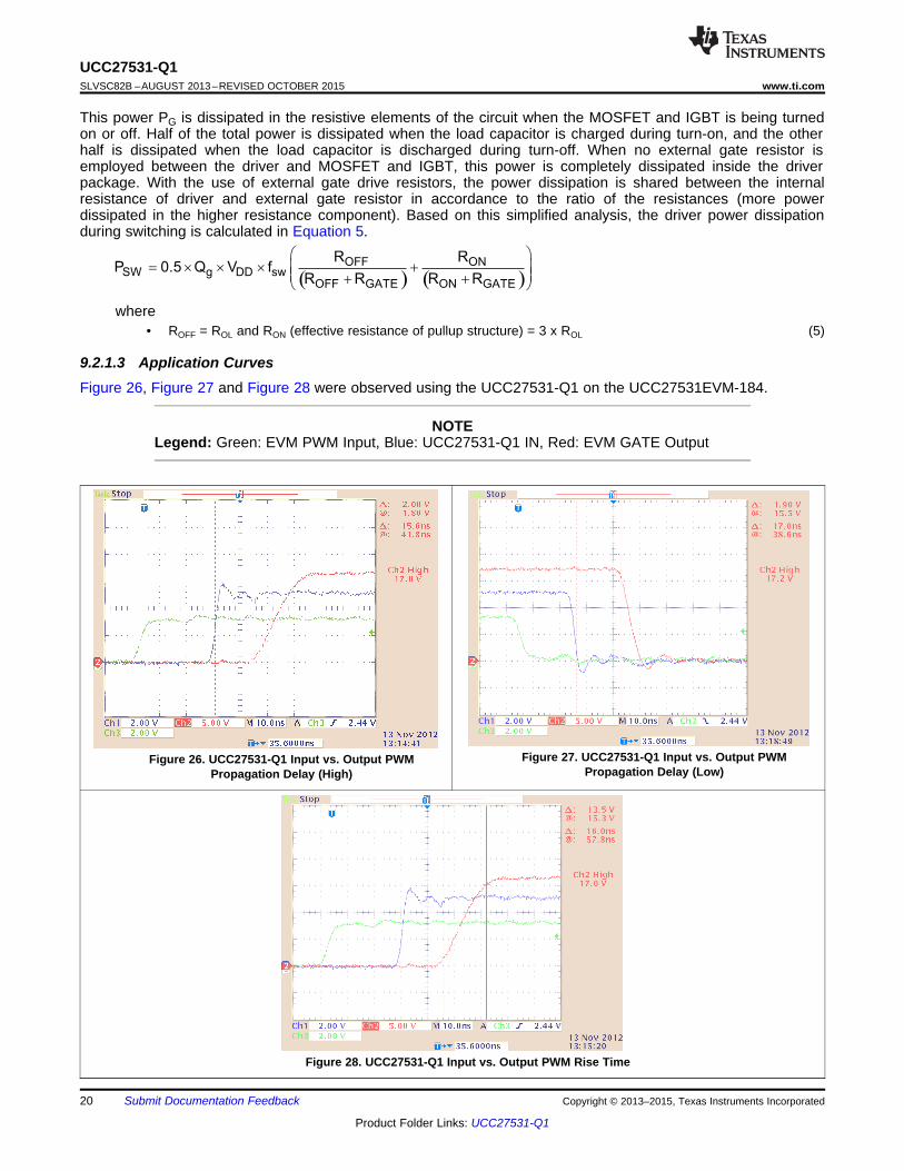
9.2.1.3 Application CurvesFigure 26, Figure 27 and Figure 28 were observed using the UCC27531-Q1 on the UCC27531EVM-184.
NOTELegend: Green: EVM PWM Input, Blue: UCC27531-Q1 IN, Red: EVM GATE Output
Figure 27. UCC27531-Q1 Input vs. Output PWMFigure 26. UCC27531-Q1 Input vs. Output PWMPropagation Delay (Low)Propagation Delay (High)
Figure 28. UCC27531-Q1 Input vs. Output PWM Rise Time
20 Submit Documentation Feedback Copyright © 2013–2015, Texas Instruments Incorporated
Product Folder Links: UCC27531-Q1
1
2
3
6
5
4
+
EN
IN
VDD
OUTH
OUTL
GND
+
–
+
–
13 V
18 V
UCC27531-Q1
UCC27531-Q1www.ti.com SLVSC82B –AUGUST 2013–REVISED OCTOBER 2015
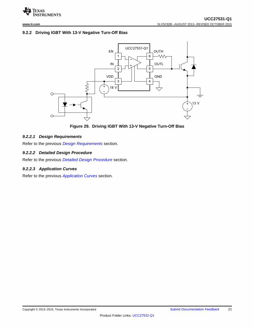
9.2.2 Driving IGBT With 13-V Negative Turn-Off Bias
Figure 29. Driving IGBT With 13-V Negative Turn-Off Bias
9.2.2.1 Design RequirementsRefer to the previous Design Requirements section.
9.2.2.2 Detailed Design ProcedureRefer to the previous Detailed Design Procedure section.
9.2.2.3 Application CurvesRefer to the previous Application Curves section.
Copyright © 2013–2015, Texas Instruments Incorporated Submit Documentation Feedback 21
Product Folder Links: UCC27531-Q1
Controller
+
–
+
–
Isol.
Isol.
Isol.
Isol.
UCC27531-Q1
E/2
E/2
UCC27531-Q1
UCC27531-Q1
UCC27531-Q1
UCC27531-Q1SLVSC82B –AUGUST 2013–REVISED OCTOBER 2015 www.ti.com
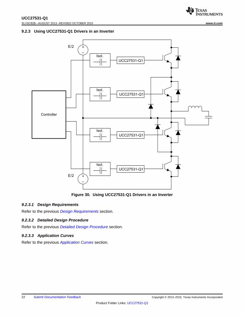
9.2.3 Using UCC27531-Q1 Drivers in an Inverter
Figure 30. Using UCC27531-Q1 Drivers in an Inverter
9.2.3.1 Design RequirementsRefer to the previous Design Requirements section.
9.2.3.2 Detailed Design ProcedureRefer to the previous Detailed Design Procedure section.
9.2.3.3 Application CurvesRefer to the previous Application Curves section.
22 Submit Documentation Feedback Copyright © 2013–2015, Texas Instruments Incorporated
Product Folder Links: UCC27531-Q1
UCC27531-Q1www.ti.com SLVSC82B –AUGUST 2013–REVISED OCTOBER 2015
10 Power Supply RecommendationsThe bias supply voltage range for which the UCC2753x devices are rated to operate is from 10 V to 32 V. Thelower end of this range is governed by the internal UVLO protection feature on the VDD pin supply circuit blocks.Whenever the driver is in UVLO condition when the VDD pin voltage is below the V(ON) supply start threshold,this feature holds the output low, regardless of the status of the inputs. The upper end of this range is driven bythe 35-V absolute maximum voltage rating of the VDD pin of the device (which is a stress rating). Keeping a 3-Vmargin to allow for transient voltage spikes, the maximum recommended voltage for the VDD pin is 32 V.
The UVLO protection feature also involves a hysteresis function. This means that when the VDD pin bias voltagehas exceeded the threshold voltage and device begins to operate, and if the voltage drops, then the devicecontinues to deliver normal functionality unless the voltage drop exceeds the hysteresis specification VDD(hys).Therefore, ensuring that, while operating at or near the 9.8 V range, the voltage ripple on the auxiliary powersupply output is smaller than the hysteresis specification of the device is important to avoid triggering deviceshutdown.
During system shutdown, the device operation continues until the VDD pin voltage has dropped below theV(OFF) threshold which must be accounted for while evaluating system shutdown timing design requirements.Likewise, at system start-up, the device does not begin operation until the VDD pin voltage has exceeded abovethe V(ON) threshold. The quiescent current consumed by the internal circuit blocks of the device is suppliedthrough the VDD pin. Although this fact is well known, recognizing that the charge for source current pulsesdelivered by the OUT pin is also supplied through the same VDD pin is important. As a result, every time acurrent is sourced out of the output pin (OUT), a corresponding current pulse is delivered into the device throughthe VDD pin. Thus ensuring that local bypass capacitors are provided between the VDD and GND pins andlocated as close to the device as possible for the purpose of decoupling is important. A low-ESR, ceramicsurface-mount capacitor is mandatory.
11 Layout
11.1 Layout GuidelinesProper PCB layout is extremely important in a high current, fast switching circuit to provide appropriate deviceoperation and design robustness. The UCC27531-Q1 gate driver incorporates short propagation delays andpowerful output stages capable of delivering large current peaks with very fast rise and fall times at the gate ofpower switch to facilitate voltage transitions very quickly. At higher VDD voltages, the peak current capability iseven higher (2.5-A and 5-A peak current is at VDD = 18 V). Very high di/dt can cause unacceptable ringing if thetrace lengths and impedances are not well controlled. The following circuit layout guidelines are stronglyrecommended when designing with these high-speed drivers.• Locate the driver device as close as possible to power device in order to minimize the length of high-current
traces between the driver Output pins and the gate of the power switch device.• Locate the VDD bypass capacitors between VDD and GND as close as possible to the driver with minimal
trace length to improve the noise filtering. These capacitors support high peak current being drawn from VDDduring turn-on of power switch. The use of low inductance SMD components such as chip resistors and chipcapacitors is highly recommended.
• The turn-on and turn-off current loop paths (driver device, power switch and VDD bypass capacitor) should beminimized as much as possible in order to keep the stray inductance to a minimum. High di/dt is establishedin these loops at two instances – during turn-on and turn-off transients, which induces significant voltagetransients on the output pins of the driver device and gate of the power switch.
• Wherever possible, parallel the source and return traces of a current loop, taking advantage of fluxcancellation
• Separate power traces and signal traces, such as output and input signals.• Star-point grounding is a good way to minimize noise coupling from one current loop to another. The GND of
the driver should be connected to the other circuit nodes such as source of power switch, ground of PWMcontroller etc at one, single point. The connected paths should be as short as possible to reduce inductanceand be as wide as possible to reduce resistance.
• Use a ground plane to provide noise shielding. Fast rise and fall times at OUT may corrupt the input signalsduring transition. The ground plane must not be a conduction path for any current loop. Instead the groundplane must be connected to the star-point with one single trace to establish the ground potential. In additionto noise shielding, the ground plane can help in power dissipation as well.
Copyright © 2013–2015, Texas Instruments Incorporated Submit Documentation Feedback 23
Product Folder Links: UCC27531-Q1
UCC27531-Q1SLVSC82B –AUGUST 2013–REVISED OCTOBER 2015 www.ti.com
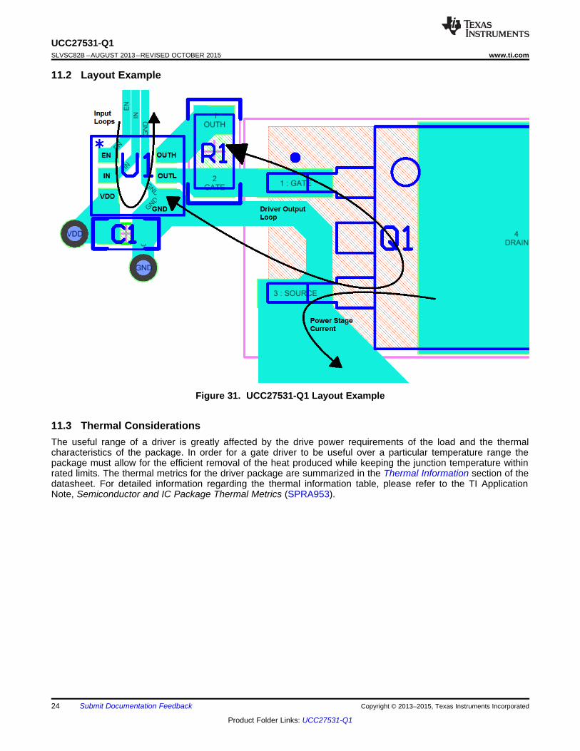
11.2 Layout Example
Figure 31. UCC27531-Q1 Layout Example
11.3 Thermal ConsiderationsThe useful range of a driver is greatly affected by the drive power requirements of the load and the thermalcharacteristics of the package. In order for a gate driver to be useful over a particular temperature range thepackage must allow for the efficient removal of the heat produced while keeping the junction temperature withinrated limits. The thermal metrics for the driver package are summarized in the Thermal Information section of thedatasheet. For detailed information regarding the thermal information table, please refer to the TI ApplicationNote, Semiconductor and IC Package Thermal Metrics (SPRA953).
24 Submit Documentation Feedback Copyright © 2013–2015, Texas Instruments Incorporated
Product Folder Links: UCC27531-Q1
UCC27531-Q1www.ti.com SLVSC82B –AUGUST 2013–REVISED OCTOBER 2015
12 Device and Documentation Support
12.1 Community ResourcesThe following links connect to TI community resources. Linked contents are provided "AS IS" by the respectivecontributors. They do not constitute TI specifications and do not necessarily reflect TI's views; see TI's Terms ofUse.
TI E2E™ Online Community TI's Engineer-to-Engineer (E2E) Community. Created to foster collaborationamong engineers. At e2e.ti.com, you can ask questions, share knowledge, explore ideas and helpsolve problems with fellow engineers.
Design Support TI's Design Support Quickly find helpful E2E forums along with design support tools andcontact information for technical support.
12.2 TrademarksE2E is a trademark of Texas Instruments.All other trademarks are the property of their respective owners.
12.3 Electrostatic Discharge CautionThese devices have limited built-in ESD protection. The leads should be shorted together or the device placed in conductive foamduring storage or handling to prevent electrostatic damage to the MOS gates.
12.4 GlossarySLYZ022 — TI Glossary.
This glossary lists and explains terms, acronyms, and definitions.
13 Mechanical, Packaging, and Orderable InformationThe following pages include mechanical, packaging, and orderable information. This information is the mostcurrent data available for the designated devices. This data is subject to change without notice and revision ofthis document. For browser-based versions of this data sheet, refer to the left-hand navigation.
Copyright © 2013–2015, Texas Instruments Incorporated Submit Documentation Feedback 25
Product Folder Links: UCC27531-Q1
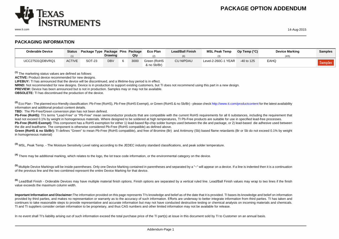
PACKAGE OPTION ADDENDUM
www.ti.com 14-Aug-2015
Addendum-Page 1
PACKAGING INFORMATION
Orderable Device Status(1)
Package Type PackageDrawing
Pins PackageQty
Eco Plan(2)
Lead/Ball Finish(6)
MSL Peak Temp(3)
Op Temp (°C) Device Marking(4/5)
Samples
UCC27531QDBVRQ1 ACTIVE SOT-23 DBV 6 3000 Green (RoHS& no Sb/Br)
CU NIPDAU Level-2-260C-1 YEAR -40 to 125 EAHQ
(1) The marketing status values are defined as follows:ACTIVE: Product device recommended for new designs.LIFEBUY: TI has announced that the device will be discontinued, and a lifetime-buy period is in effect.NRND: Not recommended for new designs. Device is in production to support existing customers, but TI does not recommend using this part in a new design.PREVIEW: Device has been announced but is not in production. Samples may or may not be available.OBSOLETE: TI has discontinued the production of the device.
(2) Eco Plan - The planned eco-friendly classification: Pb-Free (RoHS), Pb-Free (RoHS Exempt), or Green (RoHS & no Sb/Br) - please check http://www.ti.com/productcontent for the latest availabilityinformation and additional product content details.TBD: The Pb-Free/Green conversion plan has not been defined.Pb-Free (RoHS): TI's terms "Lead-Free" or "Pb-Free" mean semiconductor products that are compatible with the current RoHS requirements for all 6 substances, including the requirement thatlead not exceed 0.1% by weight in homogeneous materials. Where designed to be soldered at high temperatures, TI Pb-Free products are suitable for use in specified lead-free processes.Pb-Free (RoHS Exempt): This component has a RoHS exemption for either 1) lead-based flip-chip solder bumps used between the die and package, or 2) lead-based die adhesive used betweenthe die and leadframe. The component is otherwise considered Pb-Free (RoHS compatible) as defined above.Green (RoHS & no Sb/Br): TI defines "Green" to mean Pb-Free (RoHS compatible), and free of Bromine (Br) and Antimony (Sb) based flame retardants (Br or Sb do not exceed 0.1% by weightin homogeneous material)
(3) MSL, Peak Temp. - The Moisture Sensitivity Level rating according to the JEDEC industry standard classifications, and peak solder temperature.
(4) There may be additional marking, which relates to the logo, the lot trace code information, or the environmental category on the device.
(5) Multiple Device Markings will be inside parentheses. Only one Device Marking contained in parentheses and separated by a "~" will appear on a device. If a line is indented then it is a continuationof the previous line and the two combined represent the entire Device Marking for that device.
(6) Lead/Ball Finish - Orderable Devices may have multiple material finish options. Finish options are separated by a vertical ruled line. Lead/Ball Finish values may wrap to two lines if the finishvalue exceeds the maximum column width.
Important Information and Disclaimer:The information provided on this page represents TI's knowledge and belief as of the date that it is provided. TI bases its knowledge and belief on informationprovided by third parties, and makes no representation or warranty as to the accuracy of such information. Efforts are underway to better integrate information from third parties. TI has taken andcontinues to take reasonable steps to provide representative and accurate information but may not have conducted destructive testing or chemical analysis on incoming materials and chemicals.TI and TI suppliers consider certain information to be proprietary, and thus CAS numbers and other limited information may not be available for release.
In no event shall TI's liability arising out of such information exceed the total purchase price of the TI part(s) at issue in this document sold by TI to Customer on an annual basis.
PACKAGE OPTION ADDENDUM
www.ti.com 14-Aug-2015
Addendum-Page 2
OTHER QUALIFIED VERSIONS OF UCC27531-Q1 :
• Catalog: UCC27531
NOTE: Qualified Version Definitions:
• Catalog - TI's standard catalog product
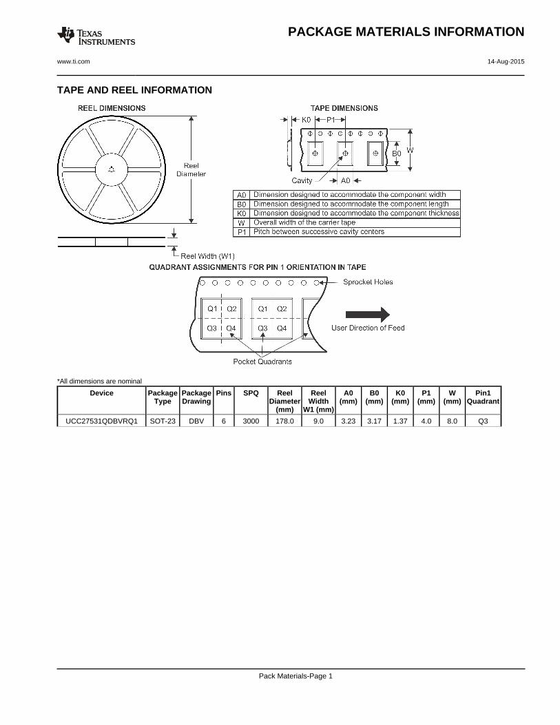
TAPE AND REEL INFORMATION
*All dimensions are nominal
Device PackageType
PackageDrawing
Pins SPQ ReelDiameter
(mm)
ReelWidth
W1 (mm)
A0(mm)
B0(mm)
K0(mm)
P1(mm)
W(mm)
Pin1Quadrant
UCC27531QDBVRQ1 SOT-23 DBV 6 3000 178.0 9.0 3.23 3.17 1.37 4.0 8.0 Q3
PACKAGE MATERIALS INFORMATION
www.ti.com 14-Aug-2015
Pack Materials-Page 1
*All dimensions are nominal
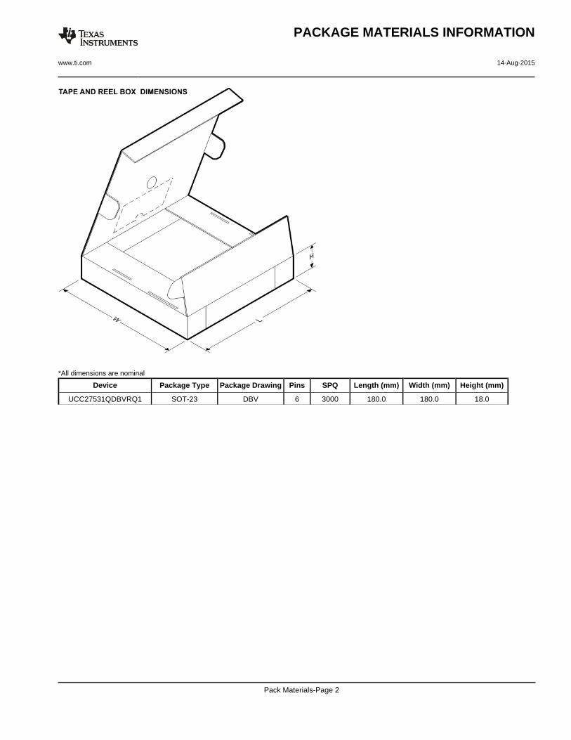
Device Package Type Package Drawing Pins SPQ Length (mm) Width (mm) Height (mm)
UCC27531QDBVRQ1 SOT-23 DBV 6 3000 180.0 180.0 18.0
PACKAGE MATERIALS INFORMATION
www.ti.com 14-Aug-2015
Pack Materials-Page 2
IMPORTANT NOTICE
Texas Instruments Incorporated and its subsidiaries (TI) reserve the right to make corrections, enhancements, improvements and otherchanges to its semiconductor products and services per JESD46, latest issue, and to discontinue any product or service per JESD48, latestissue. Buyers should obtain the latest relevant information before placing orders and should verify that such information is current andcomplete. All semiconductor products (also referred to herein as “components”) are sold subject to TI’s terms and conditions of salesupplied at the time of order acknowledgment.TI warrants performance of its components to the specifications applicable at the time of sale, in accordance with the warranty in TI’s termsand conditions of sale of semiconductor products. Testing and other quality control techniques are used to the extent TI deems necessaryto support this warranty. Except where mandated by applicable law, testing of all parameters of each component is not necessarilyperformed.TI assumes no liability for applications assistance or the design of Buyers’ products. Buyers are responsible for their products andapplications using TI components. To minimize the risks associated with Buyers’ products and applications, Buyers should provideadequate design and operating safeguards.TI does not warrant or represent that any license, either express or implied, is granted under any patent right, copyright, mask work right, orother intellectual property right relating to any combination, machine, or process in which TI components or services are used. Informationpublished by TI regarding third-party products or services does not constitute a license to use such products or services or a warranty orendorsement thereof. Use of such information may require a license from a third party under the patents or other intellectual property of thethird party, or a license from TI under the patents or other intellectual property of TI.Reproduction of significant portions of TI information in TI data books or data sheets is permissible only if reproduction is without alterationand is accompanied by all associated warranties, conditions, limitations, and notices. TI is not responsible or liable for such altereddocumentation. Information of third parties may be subject to additional restrictions.Resale of TI components or services with statements different from or beyond the parameters stated by TI for that component or servicevoids all express and any implied warranties for the associated TI component or service and is an unfair and deceptive business practice.TI is not responsible or liable for any such statements.Buyer acknowledges and agrees that it is solely responsible for compliance with all legal, regulatory and safety-related requirementsconcerning its products, and any use of TI components in its applications, notwithstanding any applications-related information or supportthat may be provided by TI. Buyer represents and agrees that it has all the necessary expertise to create and implement safeguards whichanticipate dangerous consequences of failures, monitor failures and their consequences, lessen the likelihood of failures that might causeharm and take appropriate remedial actions. Buyer will fully indemnify TI and its representatives against any damages arising out of the useof any TI components in safety-critical applications.In some cases, TI components may be promoted specifically to facilitate safety-related applications. With such components, TI’s goal is tohelp enable customers to design and create their own end-product solutions that meet applicable functional safety standards andrequirements. Nonetheless, such components are subject to these terms.No TI components are authorized for use in FDA Class III (or similar life-critical medical equipment) unless authorized officers of the partieshave executed a special agreement specifically governing such use.Only those TI components which TI has specifically designated as military grade or “enhanced plastic” are designed and intended for use inmilitary/aerospace applications or environments. Buyer acknowledges and agrees that any military or aerospace use of TI componentswhich have not been so designated is solely at the Buyer's risk, and that Buyer is solely responsible for compliance with all legal andregulatory requirements in connection with such use.TI has specifically designated certain components as meeting ISO/TS16949 requirements, mainly for automotive use. In any case of use ofnon-designated products, TI will not be responsible for any failure to meet ISO/TS16949.
Products ApplicationsAudio www.ti.com/audio Automotive and Transportation www.ti.com/automotiveAmplifiers amplifier.ti.com Communications and Telecom www.ti.com/communicationsData Converters dataconverter.ti.com Computers and Peripherals www.ti.com/computersDLP® Products www.dlp.com Consumer Electronics www.ti.com/consumer-appsDSP dsp.ti.com Energy and Lighting www.ti.com/energyClocks and Timers www.ti.com/clocks Industrial www.ti.com/industrialInterface interface.ti.com Medical www.ti.com/medicalLogic logic.ti.com Security www.ti.com/securityPower Mgmt power.ti.com Space, Avionics and Defense www.ti.com/space-avionics-defenseMicrocontrollers microcontroller.ti.com Video and Imaging www.ti.com/videoRFID www.ti-rfid.comOMAP Applications Processors www.ti.com/omap TI E2E Community e2e.ti.comWireless Connectivity www.ti.com/wirelessconnectivity
Mailing Address: Texas Instruments, Post Office Box 655303, Dallas, Texas 75265Copyright © 2015, Texas Instruments Incorporated