ct83x series - crocus technology · sot-23 package for ct834dr-is3 ana gnd vdd axis of sensitivity...
TRANSCRIPT

2018 Crocus Technology Page 1
Document Number CT83x Series Datasheet Rev 1.0
CT83x Series Omnipolar Digital TMR
Latch/Sensor for Consumer
& Industrial Applications
Features and Benefits
• High sensitivity, BOP as low as 0.9 mT
• Resistant to mechanical stress
• Ultra-low power consumption as low as 200 nA
• Digital CMOS push-pull and open drain options
• Low profile and small form factor packaging
• RoHS Compliant
Application Examples
• IoT devices
• Smartphones, tablets, and laptops
• Door or lid closure detection
• Reed switch replacement
• Motor controllers
• Proximity detection
• Power switch or open-close detection
• Tamper-proofing for utility meters
• Fluid level detection
Product Description
The CT83x Series of integrated omnipolar magnetic latches and analog sensor
are designed for consumer and industrial switching applications. It is based on
Crocus Technology’s patented Magnetic Logic Unit™ (MLU™) technology with
integrated CMOS process to provide a monolithic solution for superior sensing
performance.
This series of magnetic latches feature an industry leading low power consump-
tion as low as 200 nA. They are capable of handling large air gap applications
with low magnetic fields down to 0.9 mT with best in class high frequency perfor-
mance. The CT83x is offered in active-low push-pull CMOS and open drain con-
figuration for design flexibility. The latches are available in a low profile and small
form factor 4-lead LGA and 3-lead SOT-23 packages, providing cost effective and
space-saving solutions for high volume manufacturing. Please contact factory for
custom solutions.
SOT-23 Package
1.40 x 1.40 x 0.44 mm LGA

2018 Crocus Technology Page 2
Document Number CT83x Series Datasheet Rev 1.0
CT83x Series Omnipolar Digital TMR
Latch/Sensor for Consumer
& Industrial Applications
Figure 1: CT83x Block Diagrams
AnalogFront-End
State Machine
OscillatorUVLO Biases
Open Drain/
Push-pullOutput
GND
3
MLU OUT2
1
VDD
AnalogFront-End
State Machine
OscillatorUVLO Biases
Analog Output
GND
3
MLU ANA2
1
VDD
CT83x (SOT23 Package) Block Diagram
CT834 (SOT23 Package) Block Diagram
2018 Crocus Technology Page 3
Document Number CT83x Series Datasheet Rev 1.0
CT83x Series Omnipolar Digital TMR
Latch/Sensor for Consumer
& Industrial Applications
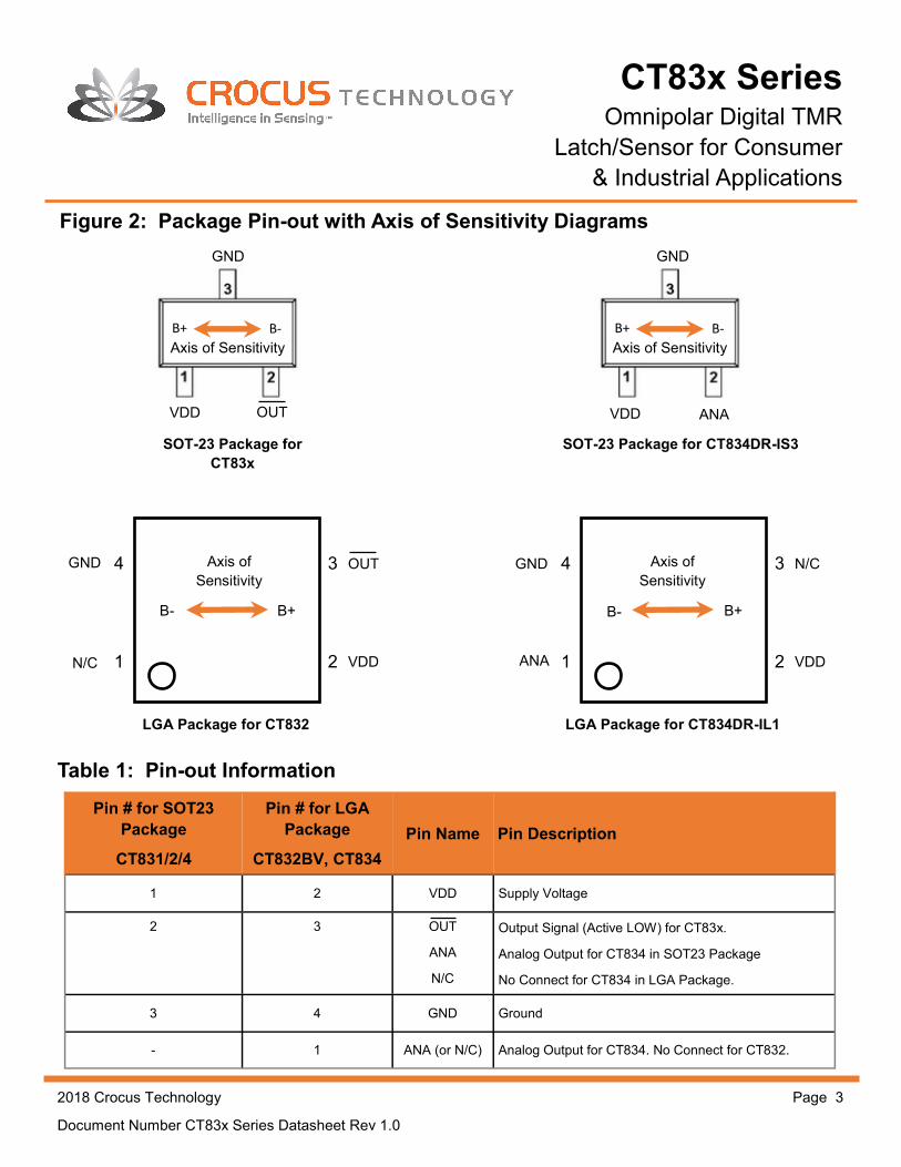
Pin # for SOT23
Package
CT831/2/4
Pin # for LGA
Package
CT832BV, CT834
Pin Name Pin Description
1 2 VDD Supply Voltage
2 3 OUT
ANA
N/C
Output Signal (Active LOW) for CT83x.
Analog Output for CT834 in SOT23 Package
No Connect for CT834 in LGA Package.
3 4 GND Ground
- 1 ANA (or N/C) Analog Output for CT834. No Connect for CT832.
Table 1: Pin-out Information
Figure 2: Package Pin-out with Axis of Sensitivity Diagrams
OUT
GND
VDD
SOT-23 Package for
CT83x
Axis of Sensitivity
B+ B-
SOT-23 Package for CT834DR-IS3
ANA
GND
VDD
Axis of Sensitivity
B+ B-
4
1 2
3
LGA Package for CT832
GND
N/C VDD
OUT Axis of
Sensitivity
B- B+
4
1 2
3
LGA Package for CT834DR-IL1
GND
ANA VDD
N/C Axis of
Sensitivity
B- B+

2018 Crocus Technology Page 4
Document Number CT83x Series Datasheet Rev 1.0
CT83x Series Omnipolar Digital TMR
Latch/Sensor for Consumer
& Industrial Applications
Table 2: Absolute Maximum Ratings
Parameter Symbol Min Max Unit
Supply Voltage VDD -0.3 4.0 V
Push-pull Output (Active LOW) VOUT_PP -0.3 VDD + 0.3 V
Open Drain Output Voltage (Active LOW) VOUT_OD -0.3 5.5 V
Analog Output VANA -0.3 VDD + 0.3 V
Input and Output Current IIN / IOUT -10 +10 mA
Junction temperature TJ -40 +125 °C
Storage temperature TSTG -65 +150 °C
Soldering temperature TSOL +260 °C
ESD Level, Human Body Model per JESD22-A114 VESD_HBM ±4.0 kV
Parameter Symbol Conditions Min Typ Max Unit
Supply Voltage VDD 2.7 3.0 3.6 V
Output Voltage VOUT 3.6 V
Operating Magnetic Flux B 12 mT
Ambient Temperature TA -40 +25 +125 °C
Junction Temperature TJ -40 +125 °C
Exceeding the absolute maximum ratings may cause permanent damage. Exposure to absolute maximum rated
conditions for extended periods may affect device reliability.
Table 3: Recommended Operating Conditions
The Recommended Operating Conditions table defines the conditions for the actual device operation. Recommend-
ed operating conditions are specified to ensure optimal performance to the data sheet specifications. Crocus Tech-
nology does not recommend exceeding them or designing to absolute maximum ratings.
Parameter Symbol Min Typ Max Unit
Junction-to-Ambient Thermal Resistance for SOT23 Package JA(SOT23) 202 °C/W
Junction-to-Ambient Thermal Resistance for LGA Package JA(LGA) 165 °C/W
Table 4: Thermal Properties
Junction-to-ambient thermal resistance is a function of application and board layout and is determined in accord-
ance to JEDEC standard JESD51 for a four (4) layer 2s2p FR-4 printed circuit board (PCB). Special attention must
be paid not to exceed junction temperature TJ(MAX) at a given ambient temperature.

2018 Crocus Technology Page 5
Document Number CT83x Series Datasheet Rev 1.0
CT83x Series Omnipolar Digital TMR
Latch/Sensor for Consumer
& Industrial Applications
Table 5: Electrical Characteristics for CT83x Series
Unless otherwise specified: VDD = 2.7 V to 3.6 V, TA = -40°C to +125°C. Typical values are VDD = 3.0 V and TA = +25°C.
Parameter Symbol Conditions Min Typ Max Unit
Power-On Time tON VDD > 2.7 V 500 µs
Under-voltage Lockout Threshold, Rising VDD
VUVLO_RISE Rising VDD 2.20 2.60 V
Under-voltage Lockout Threshold, Falling VDD
VUVLO_FALL Falling VDD 1.90 2.15 V
Under-voltage Lockout Hysteresis VUV_HYST 50 mV
Push-Pull Output
Output Voltage High OUT VOH IOUT = -2 mA 0.9 VDD V
Output Voltage Low OUT VOL IOUT = +2 mA 0.1 VDD V
Current for OUT IOUT ±2 mA
Open Drain Output
High Level Output Voltage VOH 5.5 V
Low Level Output Voltage VOL IOUT ≤ 20 mA 0 0.5 V
High Impedance Output Leakage Current (1)
ILEAK VOH = 5.5 V, B = 0 20 pA
Typical Timing Characteristics for CT83x
VDD = 3.0 V and TA = +25°C, CDD = 1.0 µF (unless otherwise specified).
Figure 3. Power-On Time for Push-pull Output (VDD
and OUT)
Figure 4. Power-On Time for Open Drain Output (VDD
and OUT)
(1) Guaranteed by design and bench characterization.

2018 Crocus Technology Page 6
Document Number CT83x Series Datasheet Rev 1.0
CT83x Series Omnipolar Digital TMR
Latch/Sensor for Consumer
& Industrial Applications
Table 6: Electrical & Magnetic Characteristics for CT831BV
Unless otherwise specified: VDD = 2.7 V to 3.6 V, TA = -40°C to +125°C. Typical values are VDD = 3.0 V and TA = +25°C.
Parameter Symbol Conditions Min Typ Max Unit
Average Supply Current IDD(AVG) t 10 s 200 700 nA
Sampling Frequency fS 1 2 4 Hz
Active Mode Time tACT 1.40 µs
Idle Mode Time tIDLE 250 500 1,000 ms
Operate Point BOPS 2.7 3.0 3.8 mT
Operate Point BOPN -3.8 -3.0 -2.7 mT
Release point BRPS 1.8 2.0 2.7 mT
Release point BRPN -2.7 -2.0 -1.8 mT
Hysteresis BHYST BHYST = BOP − BRP 0.5 1.0 mT
Table 7: Electrical & Magnetic Characteristics for CT832BV
Unless otherwise specified: VDD = 2.7 V to 3.6 V, TA = -40°C to +125°C. Typical values are VDD = 3.0 V and TA = +25°C.
Parameter Symbol Conditions Min Typ Max Unit
Average Supply Current IDD(AVG) t 10 s 200 700 nA
Sampling Frequency fS 1 2 4 Hz
Active Mode Time tACT 1.4 µs
Idle Mode Time tIDLE 250 500 1,000 ms
Operate Point BOPS 2.7 3.0 3.8 mT
Operate Point BOPN -3.8 -3.0 -2.7 mT
Release point BRPS 1.8 2.0 2.7 mT
Release point BRPN -2.7 -2.0 -1.8 mT
Hysteresis BHYST BHYST = BOP − BRP 0.5 1.0 mT

2018 Crocus Technology Page 7
Document Number CT83x Series Datasheet Rev 1.0
CT83x Series Omnipolar Digital TMR
Latch/Sensor for Consumer
& Industrial Applications
Figure 5. Average Supply Current vs. Supply Voltage
vs. Temperature
Figure 6. Average Supply Current vs. Temperature vs.
Supply Voltage
Typical Electrical Characteristics for CT831BV and CT832BV
VDD = 3.0 V and TA = +25°C, CDD = 1.0 µF (unless otherwise specified).
Figure 7. Sampling Frequency vs. Supply Voltage vs.
Temperature

2018 Crocus Technology Page 8
Document Number CT83x Series Datasheet Rev 1.0
CT83x Series Omnipolar Digital TMR
Latch/Sensor for Consumer
& Industrial Applications
Figure 8. BOPN (Red) and BOPS (Blue) vs. Supply Volt-
age at +25°C
Figure 9. BRPN (Red) and BRPS (Blue) vs. Supply Volt-
age at +25°C
Typical Magnetic Characteristics for CT831BV and CT832BV
VDD = 3.0 V and TA = +25°C, CDD = 1.0 µF (unless otherwise specified).
Figure 10. BOPN (Orange) and BOPS (Green) vs. Oper-
ating Temperature at VDD = 3.0 V
Figure 11. BRPN (Orange) and BRPS (Green) vs. Oper-
ating Temperature at VDD = 3.0 V

2018 Crocus Technology Page 9
Document Number CT83x Series Datasheet Rev 1.0
CT83x Series Omnipolar Digital TMR
Latch/Sensor for Consumer
& Industrial Applications
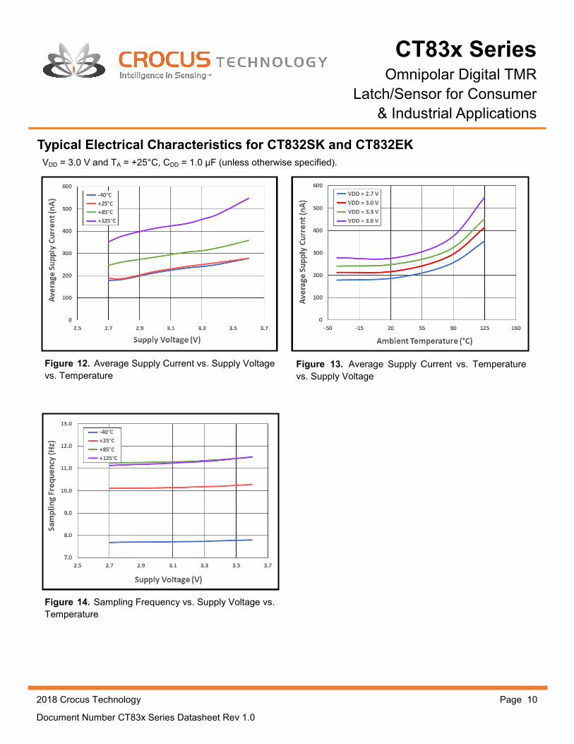
Table 8: Electrical & Magnetic Characteristics for CT832SK
Unless otherwise specified: VDD = 2.7 V to 3.6 V, TA = -40°C to +125°C. Typical values are VDD = 3.0 V and TA = +25°C.
Parameter Symbol Conditions Min Typ Max Unit
Average Supply Current IDD(AVG) t 10 s 230 700 nA
Sampling Frequency fS 7 10 13 Hz
Active Mode Time tACT 1.4 µs
Idle Mode Time tIDLE 77 100 143 ms
Operate Point BOPS 0.8 0.9 1.2 mT
Operate Point BOPN -1.2 -0.9 -0.8 mT
Release point BRPS 0.3 0.5 0.7 mT
Release point BRPN -0.7 -0.5 -0.3 mT
Hysteresis BHYST BHYST = BOP − BRP 0.3 0.4 mT
Table 9: Electrical & Magnetic Characteristics for CT832EK
Unless otherwise specified: VDD = 2.7 V to 3.6 V, TA = -40°C to +125°C. Typical values are VDD = 3.0 V and TA = +25°C.
Parameter Symbol Conditions Min Typ Max Unit
Average Supply Current IDD(AVG) t 10 s 230 700 nA
Sampling Frequency fS 7 10 13 Hz
Active Mode Time tACT 1.4 µs
Idle Mode Time tIDLE 77 100 143 ms
Operate Point BOPS 7.0 mT
Operate Point BOPN -7.0 mT
Release Point BRPS 5.0 mT
Release Point BRPN -5.0 mT
Hysteresis BHYST BHYST = BOP − BRP 2.0 mT
2018 Crocus Technology Page 10
Document Number CT83x Series Datasheet Rev 1.0
CT83x Series Omnipolar Digital TMR
Latch/Sensor for Consumer
& Industrial Applications
Figure 12. Average Supply Current vs. Supply Voltage
vs. Temperature
Figure 13. Average Supply Current vs. Temperature
vs. Supply Voltage
Typical Electrical Characteristics for CT832SK and CT832EK
VDD = 3.0 V and TA = +25°C, CDD = 1.0 µF (unless otherwise specified).
Figure 14. Sampling Frequency vs. Supply Voltage vs.
Temperature

2018 Crocus Technology Page 11
Document Number CT83x Series Datasheet Rev 1.0
CT83x Series Omnipolar Digital TMR
Latch/Sensor for Consumer
& Industrial Applications
Figure 15. BOPN (Red) and BOPS (Blue) vs. Supply
Voltage at +25°C
Figure 16. BRPN (Red) and BRPS (Blue) vs. Supply Volt-
age at +25°C
Typical Magnetic Characteristics for CT832SK
VDD = 3.0 V and TA = +25°C, CDD = 1.0 µF (unless otherwise specified).
Figure 17. BOPN (Orange) and BOPS (Green) vs. Oper-
ating Temperature at VDD = 3.0 V
Figure 18. BRPN (Orange) and BRPS (Green) vs. Oper-
ating Temperature at VDD = 3.0 V

2018 Crocus Technology Page 12
Document Number CT83x Series Datasheet Rev 1.0
CT83x Series Omnipolar Digital TMR
Latch/Sensor for Consumer
& Industrial Applications
Table 10: Electrical & Magnetic Characteristics for CT832SL
Unless otherwise specified: VDD = 2.7 V to 3.6 V, TA = -40°C to +125°C. Typical values are VDD = 3.0 V and TA = +25°C.
Parameter Symbol Conditions Min Typ Max Unit
Average Supply Current IDD(AVG) t 10 s 1.2 2.5 µA
Sampling Frequency fS 165 250 300 Hz
Active Mode Time tACT 1.4 µs
Idle Mode Time tIDLE 3.3 4.0 6.0 ms
Operate Point BOPS 0.8 0.9 1.2 mT
Operate Point BOPN -1.2 -0.9 -0.8 mT
Release point BRPS 0.3 0.5 0.7 mT
Release point BRPN -0.7 -0.5 -0.3 mT
Hysteresis BHYST BHYST = BOP − BRP 0.3 0.4 mT
Table 11: Electrical & Magnetic Characteristics for CT832BL
Unless otherwise specified: VDD = 2.7 V to 3.6 V, TA = -40°C to +125°C. Typical values are VDD = 3.0 V and TA = +25°C.
Parameter Symbol Conditions Min Typ Max Unit
Average Supply Current IDD(AVG) t 10 s 1.2 2.5 µA
Sampling Frequency fS 165 250 300 Hz
Active Mode Time tACT 1.4 µs
Idle Mode Time tIDLE 3.3 4.0 6.0 ms
Operate Point BOPS 2.7 3.0 3.8 mT
Operate Point BOPN -3.8 -3.0 -2.7 mT
Release point BRPS 1.8 2.0 2.7 mT
Release point BRPN -2.7 -2.0 -1.8 mT
Hysteresis BHYST BHYST = BOP − BRP 0.5 1.0 mT

2018 Crocus Technology Page 13
Document Number CT83x Series Datasheet Rev 1.0
CT83x Series Omnipolar Digital TMR
Latch/Sensor for Consumer
& Industrial Applications
Figure 19. Average Supply Current vs. Supply Voltage
vs. Temperature
Figure 20. Average Supply Current vs. Temperature
vs. Supply Voltage
Typical Electrical Characteristics for CT832SL and CT832BL
VDD = 3.0 V and TA = +25°C, CDD = 1.0 µF (unless otherwise specified).
Figure 21. Sampling Frequency vs. Supply Voltage vs.
Temperature

2018 Crocus Technology Page 14
Document Number CT83x Series Datasheet Rev 1.0
CT83x Series Omnipolar Digital TMR
Latch/Sensor for Consumer
& Industrial Applications
Typical Magnetic Characteristics for CT832SL
VDD = 3.0 V and TA = +25°C, CDD = 1.0 µF (unless otherwise specified).
Figure 22. BOPN (Red) and BOPS (Blue) vs. Supply
Voltage at +25°C
Figure 23. BRPN (Red) and BRPS (Blue) vs. Supply Volt-
age at +25°C
Figure 24. BOPN (Orange) and BOPS (Green) vs. Oper-
ating Temperature at VDD = 3.0 V
Figure 25. BRPN (Orange) and BRPS (Green) vs. Oper-
ating Temperature at VDD = 3.0 V

2018 Crocus Technology Page 15
Document Number CT83x Series Datasheet Rev 1.0
CT83x Series Omnipolar Digital TMR
Latch/Sensor for Consumer
& Industrial Applications
Figure 26. BOPN (Red) and BOPS (Blue) vs. Supply
Voltage at +25°C
Figure 27. BRPN (Red) and BRPS (Blue) vs. Supply Volt-
age at +25°C
Typical Magnetic Characteristics for CT832BL
VDD = 3.0 V and TA = +25°C, CDD = 1.0 µF (unless otherwise specified).
Figure 28. BOPN (Orange) and BOPS (Green) vs. Oper-
ating Temperature at VDD = 3.0 V
Figure 29. BRPN (Orange) and BRPS (Green) vs. Oper-
ating Temperature at VDD = 3.0 V

2018 Crocus Technology Page 16
Document Number CT83x Series Datasheet Rev 1.0
CT83x Series Omnipolar Digital TMR
Latch/Sensor for Consumer
& Industrial Applications
Table 12: Electrical & Magnetic Characteristics for CT832DM
Unless otherwise specified: VDD = 2.7 V to 3.6 V, TA = -40°C to +125°C. Typical values are VDD = 3.0 V and TA = +25°C.
Parameter Symbol Conditions Min Typ Max Unit
Average Supply Current IDD(AVG) t 10 s 8.0 13.0 µA
Sampling Frequency fS 1.63 2.50 3.25 kHz
Active Mode Time tACT 1.4 µs
Idle Mode Time tIDLE 308 400 614 µs
Operate Point BOPS 1.3 1.5 1.8 mT
Operate Point BOPN -1.8 -1.5 -1.3 mT
Release point BRPS 0.8 1.0 1.3 mT
Release point BRPN -1.3 -1.0 -0.8 mT
Hysteresis BHYST BHYST = BOP − BRP 0.3 0.5 mT

2018 Crocus Technology Page 17
Document Number CT83x Series Datasheet Rev 1.0
CT83x Series Omnipolar Digital TMR
Latch/Sensor for Consumer
& Industrial Applications
Figure 32. Sampling Frequency vs. Supply Voltage vs.
Temperature
Typical Electrical Characteristics for CT832DM
VDD = 3.0 V and TA = +25°C, CDD = 1.0 µF (unless otherwise specified).
Figure 30. Average Supply Current vs. Supply Voltage
vs. Temperature
Figure 31. Average Supply Current vs. Temperature
vs. Supply Voltage

2018 Crocus Technology Page 18
Document Number CT83x Series Datasheet Rev 1.0
CT83x Series Omnipolar Digital TMR
Latch/Sensor for Consumer
& Industrial Applications
Typical Magnetic Characteristics for CT832DM
VDD = 3.0 V and TA = +25°C, CDD = 1.0 µF (unless otherwise specified).
Figure 33. BOPN (Red) and BOPS (Blue) vs. Supply
Voltage at +25°C
Figure 34. BRPN (Red) and BRPS (Blue) vs. Supply Volt-
age at +25°C
Figure 35. BOPN (Orange) and BOPS (Green) vs. Oper-
ating Temperature at VDD = 3.0 V
Figure 36. BRPN (Orange) and BRPS (Green) vs. Oper-
ating Temperature at VDD = 3.0 V

2018 Crocus Technology Page 19
Document Number CT83x Series Datasheet Rev 1.0
CT83x Series Omnipolar Digital TMR
Latch/Sensor for Consumer
& Industrial Applications
Table 13: Electrical & Magnetic Characteristics for CT832BH
Unless otherwise specified: VDD = 2.7 V to 3.6 V, TA = -40°C to +125°C. Typical values are VDD = 3.0 V and TA = +25°C.
Parameter Symbol Conditions Min Typ Max Unit
Average Supply Current IDD(AVG) t 10 s 36 µA
Sampling Frequency fS 7 10 13 kHz
Active Mode Time tACT 1.4 µs
Idle Mode Time tIDLE 77 100 143 µs
Operate Point BOPS 2.7 3.0 3.8 mT
Operate Point BOPN -3.8 -3.0 -2.7 mT
Release Point BRPS 1.8 2.0 2.7 mT
Release Point BRPN -2.7 -2.0 -1.8 mT
Hysteresis BHYST BHYST = BOP − BRP 0.5 1.0 mT

2018 Crocus Technology Page 20
Document Number CT83x Series Datasheet Rev 1.0
CT83x Series Omnipolar Digital TMR
Latch/Sensor for Consumer
& Industrial Applications
Figure 39. Sampling Frequency vs. Supply Voltage vs.
Temperature
Typical Electrical Characteristics for CT832BH
VDD = 3.0 V and TA = +25°C, CDD = 1.0 µF (unless otherwise specified).
Figure 37. Average Supply Current vs. Supply Voltage
vs. Temperature
Figure 38. Average Supply Current vs. Temperature
vs. Supply Voltage

2018 Crocus Technology Page 21
Document Number CT83x Series Datasheet Rev 1.0
CT83x Series Omnipolar Digital TMR
Latch/Sensor for Consumer
& Industrial Applications
Figure 40. BOPN (Red) and BOPS (Blue) vs. Supply
Voltage at +25°C
Figure 41. BRPN (Red) and BRPS (Blue) vs. Supply Volt-
age at +25°C
Typical Magnetic Characteristics for CT832BH
VDD = 3.0 V and TA = +25°C, CDD = 1.0 µF (unless otherwise specified).
Figure 42. BOPN (Orange) and BOPS (Green) vs. Oper-
ating Temperature at VDD = 3.0 V
Figure 43. BRPN (Orange) and BRPS (Green) vs. Oper-
ating Temperature at VDD = 3.0 V

2018 Crocus Technology Page 22
Document Number CT83x Series Datasheet Rev 1.0
CT83x Series Omnipolar Digital TMR
Latch/Sensor for Consumer
& Industrial Applications
Table 14: Electrical & Magnetic Characteristics for CT834DR
Unless otherwise specified: VDD = 2.7 V to 3.6 V, TA = -40°C to +85°C. Typical values are VDD = 3.0 V and TA = +25°C.
Parameter Symbol Conditions Min Typ Max Unit
Operating Temperature TA -40 +25 +85 °C
Average Supply Current IDD(AVG) t 10 s 1.5 2.7 mA
Maximum Drive Capability IDRV(MAX)
VANA covers 19% VDD to 81% VDD
span -10 +10 µA
Output Capacitive Load CL 10 pF
Analog Output Magnetic Field
Range BANA ±1.0 ±1.5 mT
Analog Output Voltage, High VANA_HIGH 0.81 VDD V
Analog Output Voltage, Low VANA_LOW 0.19 VDD V
Voltage Output Quiescent VOQ 45 50 55 % VDD
Sensitivity @ T = +25°C ST=25 TA = +25°C 176 200 224 mV/V/mT
Sensitivity @ Full Temperature
Range SFULL_RANGE TA = -40°C to +85°C 140 200 260 mV/V/mT
Figure 44. Average Supply Current vs. Supply Voltage
vs. Temperature
Figure 45. Average Supply Current vs. Temperature
vs. Supply Voltage
Typical Characteristics for CT834DR
VDD = 3.0 V and TA = +25°C, CDD = 1.0 µF (unless otherwise specified).

2018 Crocus Technology Page 23
Document Number CT83x Series Datasheet Rev 1.0
CT83x Series Omnipolar Digital TMR
Latch/Sensor for Consumer
& Industrial Applications
Typical Magnetic Characteristics for CT834DR
VDD = 3.0 V and TA = +25°C, CDD = 1.0 µF (unless otherwise specified).
Figure 46. Magnetic Sensitivity vs. Temperature for
Positive and Negative Fields
Figure 47. Voltage Output Quiescent (VOQ) vs. Supply
Voltage vs. Temperature
Figure 48. Magnetic Sensitivity vs. Supply Voltage vs.
Temperature for Positive Field
Figure 49. Magnetic Sensitivity vs. Supply Voltage vs.
Temperature for Negative Field

2018 Crocus Technology Page 24
Document Number CT83x Series Datasheet Rev 1.0
CT83x Series Omnipolar Digital TMR
Latch/Sensor for Consumer
& Industrial Applications
Output Behavior vs. Magnetic Field
Figure 50: Omnipolar Magnetic Flux
Characteristic Conditions Output
Positive Field
B > BOPS Low (ON)
0 < B < BRPS High (OFF)
Negative Field
B < BOPN Low (ON)
0 > B > BRPN High (OFF)
B+ Field B- Field

2018 Crocus Technology Page 25
Document Number CT83x Series Datasheet Rev 1.0
CT83x Series Omnipolar Digital TMR
Latch/Sensor for Consumer
& Industrial Applications
For the analog output, a simple RC filter is recommended on the ANA output as shown below:
CT834 Analog Output
Figure 51: Application Circuits
A decoupling capacitor (CDD) between the supply voltage and ground is required with placement close to
the magnetic switch. A typical capacitor value of 1 μF (Ceramic) will suffice. For the open drain output,
maximum VSYS should not exceed 5.5 V.
CT832 Digital Output CT831 Open Drain Output

2018 Crocus Technology Page 26
Document Number CT83x Series Datasheet Rev 1.0
CT83x Series Omnipolar Digital TMR
Latch/Sensor for Consumer
& Industrial Applications
Figure 52: MLU Sensor Location
Symbols Nominal Dimensions
(mm)
A 1.60
B 2.90
C 0.80
D 1.45
D
B
C
A
1 2
3
Symbols Nominal Dimensions
(mm)
A 1.40
B 1.40
C 0.50
D 0.50
4
1 2
3
LGA Package
A
B
D
C
SOT23 Package

2018 Crocus Technology Page 27
Document Number CT83x Series Datasheet Rev 1.0
CT83x Series Omnipolar Digital TMR
Latch/Sensor for Consumer
& Industrial Applications
Table 15: Order Guide for Omnipolar TMR Digital Latches/Analog Sensors
Part Number Polarity Output Type
BOP BRP IDD(AVG) fS Description
CT831BV-HS3
CT831BV-IS3
Omnipolar
Open Drain
±3.0 mT ±2.0 mT 200 nA 2 Hz
Omnipolar Magnetic Latch SOT-23 Package, Tape & Reel Packaging
CT832BV-HL1
CT832BV-IL1
Push-Pull
Omnipolar Magnetic Latch LGA Package, Tape & Reel Packaging
CT832BV-HS3
CT832BV-IS3
Omnipolar Magnetic Latch SOT-23 Package, Tape & Reel Packaging
CT832SK-HS3
CT832SK-IS3
±0.9 mT ±0.5 mT 230 nA 10 Hz Omnipolar Magnetic Latch
SOT-23Package, Tape & Reel Packaging
CT832SL-HS3
CT832SL-IS3
±0.9 mT ±0.5 mT 1.4 µA 250 Hz Omnipolar Magnetic Latch
SOT-23 Package, Tape & Reel Packaging
CT832BL-HS3
CT832BL-IS3
±3.0 mT ±2.0 mT 1.4 µA 250 Hz Omnipolar Magnetic Latch
SOT-23 Package, Tape & Reel Packaging
CT832DM-HS3
CT832DM-IS3
±1.5 mT ±1.0 mT 12 µA 2.5 kHz Omnipolar Magnetic Latch
SOT-23 Package, Tape & Reel Packaging
CT832BH-HL1
CT832BH-IL1
±3.0 mT ±2.0 mT 36 µA 10 kHz Omnipolar Magnetic Latch
LGA Package, Tape & Reel Packaging
CT832EK-HS3
CT832EK-IS3
±7.0 mT ±5.0 mT 230 nA 10 Hz Omnipolar Magnetic Latch
SOT-23 Packages, Tape & Reel Packaging
CT834DR-IL1
Analog N/A N/A 1.5 mA Continuous
Omnipolar Magnetic Latch LGA Packages, Tape & Reel Packaging
CT834DR-IS3 Omnipolar Magnetic Latch
SOT-23 Packages, Tape & Reel Packaging

2018 Crocus Technology Page 28
Document Number CT83x Series Datasheet Rev 1.0
CT83x Series Omnipolar Digital TMR
Latch/Sensor for Consumer
& Industrial Applications
Orderable Part
Number
Package
Type Pins
Package
Quantity
Lead
Finish Eco Plan(1)
MSL Rating(2)
Operating
Temperature
Device Marking(3)
CT831BV-HS3 SOT-23 3 3,000 Sn Green & RoHS 1 -40°C to +125°C JA YWWS
CT831BV-IS3 SOT-23 3 3,000 Sn Green & RoHS 1 -40°C to +85°C JA YWWS
CT832BV-HL1 LGA 4 3,000 Au Green & RoHS 3 -40°C to +125°C A YZ
CT832BV-IL1 LGA 4 3,000 Au Green & RoHS 3 -40°C to +85°C A YZ
CT832BV-HS3 SOT-23 3 3,000 Sn Green & RoHS 1 -40°C to +125°C HA YWWS
CT832BV-IS3 SOT-23 3 3,000 Sn Green & RoHS 1 -40°C to +85°C HA YWWS
CT832SK-HS3 SOT-23 3 3,000 Sn Green & RoHS 1 -40°C to +125°C HC YWWS
CT832SK-IS3 SOT-23 3 3,000 Sn Green & RoHS 1 -40°C to +85°C HC YWWS
CT832SL-HS3 SOT-23 3 3,000 Sn Green & RoHS 1 -40°C to +125°C HE YWWS
CT832SL-IS3 SOT-23 3 3,000 Sn Green & RoHS 1 -40°C to +85°C HE YWWS
CT832BL-HS3 SOT-23 3 3,000 Sn Green & RoHS 1 -40°C to +125°C HB YWWS
CT832BL-IS3 SOT-23 3 3,000 Sn Green & RoHS 1 -40°C to +85°C HB YWWS
CT832DM-HS3 SOT-23 3 3,000 Sn Green & RoHS 1 -40°C to +125°C HD YWWS
CT832DM-IS3 SOT-23 3 3,000 Sn Green & RoHS 1 -40°C to +85°C HD YWWS
CT832BH-HL1 LGA 4 3,000 Au Green & RoHS 3 -40°C to +125°C E YZ
CT832BH-IL1 LGA 4 3,000 Au Green & RoHS 3 -40°C to +85°C E YZ
CT832EK-HS3 SOT-23 3 3,000 Sn Green & RoHS 1 -40°C to +125°C HF YWWS
CT832EK-IS3 SOT-23 3 3,000 Sn Green & RoHS 1 -40°C to +85°C HF YWWS
CT834DR-IL1 LGA 4 3,000 Au Green & RoHS 3 -40°C to +85°C D YZ
CT834DR-IS3 SOT-23 3 3,000 Sn Green & RoHS 1 -40°C to +85°C HT YWWS
Table 16. Packaging Information
(1) RoHS is defined as semiconductor products that are compliant to the current EU RoHS requirements. It also will meet the requirement that
RoHS substances do not exceed 0.1% by weight in homogeneous materials. Green is defined as the content of Chlorine (Cl), Bromine (Br) and
Antimony Trioxide based flame retardants satisfy JS709B low halogen requirements of ≤ 1,000 ppm.
(2) MSL Rating = Moisture Sensitivity Level Rating as defined by JEDEC industry standard classifications.
(3) Device Marking for SOT23 is defined as XZ YWWS where XZ = part number, Y = year, WW = work week and S = sequential number. LGA is
defined as X where X = part number and YZ = date code information.
2018 Crocus Technology Page 29
Document Number CT83x Series Datasheet Rev 1.0
CT83x Series Omnipolar Digital TMR
Latch/Sensor for Consumer
& Industrial Applications
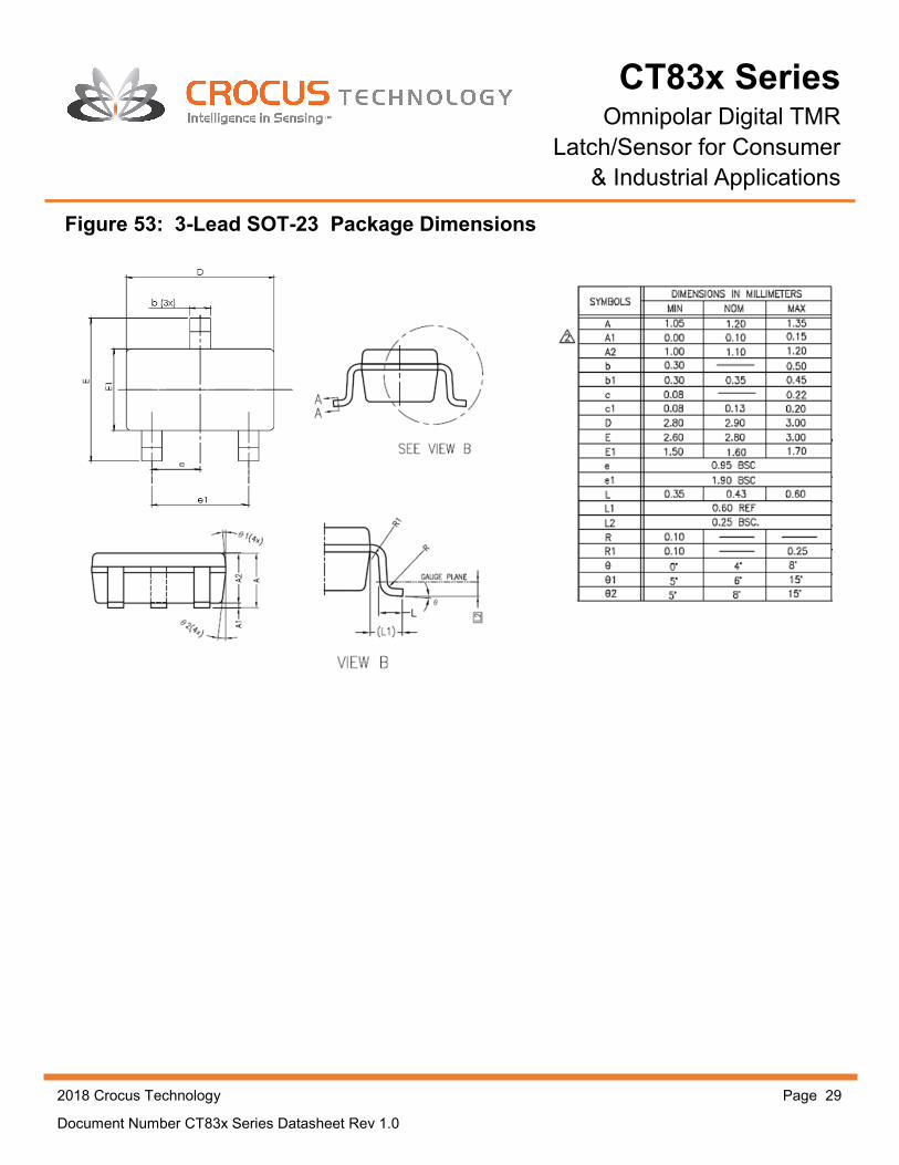
Figure 53: 3-Lead SOT-23 Package Dimensions

2018 Crocus Technology Page 30
Document Number CT83x Series Datasheet Rev 1.0
CT83x Series Omnipolar Digital TMR
Latch/Sensor for Consumer
& Industrial Applications
Figure 54: 4-Lead LGA Package Dimensions
NOTE: ALL DIMENSIONS ARE IN MILLIMETERS.

2018 Crocus Technology Page 31
Document Number CT83x Series Datasheet Rev 1.0
CT83x Series Omnipolar Digital TMR
Latch/Sensor for Consumer
& Industrial Applications
Figure 55: Tape & Pocket Dimensions for SOT23 Package
Notes:
1. Material: Conductive Polystyrene
2. Dimensions in mm.
3. 10 sprocket hole pitch cumulative tolerance ±0.2.
4. Camber not to exceed 1 mm in 100 mm.
5. Pocket position relative to sprocket hole measured
as true position of pocket, not pocket hole.
6. (S.R. /sq) means surface electric resistivity of the
carrier tape.

2018 Crocus Technology Page 32
Document Number CT83x Series Datasheet Rev 1.0
CT83x Series Omnipolar Digital TMR
Latch/Sensor for Consumer
& Industrial Applications
Figure 56: Tape & Pocket Dimensions for LGA Package

2018 Crocus Technology Page 33
Document Number CT83x Series Datasheet Rev 1.0
CT83x Series Omnipolar Digital TMR
Latch/Sensor for Consumer
& Industrial Applications
Disclaimer: The contents of this document are provided for informational purposes only. CROCUS TECHNOLOGY, INC. AND CRO-
CUS TECHNOLOGY SA (COLLECTIVELY “CROCUS”) MAKE NO REPRESENTATIONS OR WARRANTY OF ANY KIND, EX-
PRESS OR IMPLIED, WITH RESPECT TO THE ACCURACY OR COMPLETENESS OF THE CONTENTS HEREIN, INCLUDING,
BUT NOT LIMITED TO, THE IMPLIED WARRANTIES OF MERCHANTABILITY AND FITNESS FOR A PARTICULAR PURPOSE.
Crocus reserves the right to make changes to the specifications and product descriptions, and/or to discontinue or make changes to
its products at any time without notice. Crocus’s products have not been designed, tested, or manufactured for use and should not be
used in applications where the failure, malfunction or inaccuracy of the Products carries a risk of death or serious bodily injury or
damage to tangible property, including, but not limited to, life support systems, nuclear facilities, military, aircraft navigation or com-
munication, emergency systems, harsh environments, or other applications with a similar degree of potential hazard.
© 2018 Crocus Technology, Inc. and Crocus Technology SA. All rights reserved. Crocus Technology, Intelligence in Sensing, MLU,
and combinations thereof are trademarks of Crocus Technology, Inc. and Crocus Technology SA.