lmh2832 datasheet - texas · pdf filefrequency (mhz) oip3 (dbm) 0 50 100 150 200 250 300 350...
TRANSCRIPT

Frequency (MHz)
OIP
3 (d
Bm
)
0 50 100 150 200 250 300 350 400 450 500 550 60025
30
35
40
45
50
55
60
D005
Channel AChannel B
Product
Folder
Sample &Buy
Technical
Documents
Tools &
Software
Support &Community
An IMPORTANT NOTICE at the end of this data sheet addresses availability, warranty, changes, use in safety-critical applications,intellectual property matters and other important disclaimers. PRODUCTION DATA.
LMH2832SBOS709A –JULY 2016–REVISED JULY 2016
LMH2832 Fully Differential, Dual, 1.1-GHz, Digital Variable-Gain Amplifier
1
1 Features1• Dual-Channel, Individual SPI™-Controlled DVGA• Single 5-V Supply• –3-dB Bandwidth: 1.1 GHz (Max Gain)• Flat Bandwidth Response: 300 MHz• Channel-to-Channel Gain Matching: ±0.05 dB• Channel-to-Channel Phase Matching: ±0.1°• Gain:
– 30 dB to –9 dB– 1-dB Steps ±0.2 dB
• Output Third-Order Intercept Point (OIP3):– 43 dBm at 300 MHz– 51 dBm at 200 MHz
• Noise Figure (NF):– 6.5 dB (Max Gain) at 300 MHz, ZIN = 150 Ω
• Adjustable Power Consumption:– 90 mA to 108 mA per Channel
• Power-Saving, Power-Down Feature:– IQ < 4.5 mA per Channel– Power-Down Pin and SPI Programmability
• Input Return Loss at 300 MHz:– 17 dB (RS = 150 Ω)
2 Applications• DOCSIS 3.1 CMTS Upstream Direct Sampling
Receivers• CATV Modem Signal Scaling• Programmable Gain IF Amplifiers• Generic RF, IF Gain Stages• ADC Drivers
3 DescriptionThe LMH2832 is a high-linearity, dual-channel, digitalvariable-gain amplifier (DVGA) for high-speed signalchain and data-acquisition systems. The LMH2832 isoptimized to provide high bandwidth, low distortion,and low noise, thus making the device ideally suitedas a dual, 14-bit, analog-to-digital converter (ADC)driver. The device consists of one fixed-gain blockand one variable attenuator consisting of a total gainof 30 dB with a maximum attenuation of 39 dB. Thegain range is from 30 dB to –9 dB in 1-dB gain stepswith a gain accuracy of ±0.2 dB. The input impedancecan be easily matched to 50-Ω or 75-Ω systems usinga 1:3-Ω or 1:2-Ω ratio balun, respectively. TheLMH2832 is designed to drive general-purpose ADCsand also meets the requirements for both data overcable service interface specification (DOCSIS) 3.0 32quadrature amplitude modulation (QAM) carriers andDOCSIS 3.1 wideband orthogonal frequency-divisionmultiplexing (OFDM) systems. With excellent NF(6.5 dB) and linearity, the LMH2832 is designed toperform to within DOCSIS specifications. Thequiescent current in the power-down state is lessthan 5 mA per channel with the typical currentconsumption during operation at 105 mA per channel.
Device Information(1)
PART NUMBER PACKAGE BODY SIZE (NOM)LMH2832 VQFN (40) 6.00 mm × 6.00 mm
(1) For all available packages, see the orderable addendum atthe end of the data sheet.
Output Third-Order Intercept Point (OIP3) Performance

2
LMH2832SBOS709A –JULY 2016–REVISED JULY 2016 www.ti.com
Product Folder Links: LMH2832
Submit Documentation Feedback Copyright © 2016, Texas Instruments Incorporated
Table of Contents1 Features .................................................................. 12 Applications ........................................................... 13 Description ............................................................. 14 Revision History..................................................... 25 Device Comparison Table ..................................... 36 Pin Configuration and Functions ......................... 37 Specifications......................................................... 5
7.1 Absolute Maximum Ratings ...................................... 57.2 ESD Ratings.............................................................. 57.3 Recommended Operating Conditions....................... 57.4 Thermal Information .................................................. 57.5 Electrical Characteristics........................................... 67.6 Timing Requirements: SPI ........................................ 87.7 Typical Characteristics .............................................. 9
8 Parameter Measurement Information ................ 168.1 Setup Diagrams ...................................................... 168.2 ATE Testing and DC Measurements ...................... 178.3 Frequency Response .............................................. 178.4 Distortion ................................................................. 178.5 Noise Figure............................................................ 178.6 Pulse Response, Slew Rate, and Overdrive
Recovery .................................................................. 188.7 Power-Down............................................................ 188.8 Crosstalk, Gain Matching, and Phase Matching..... 188.9 Output Measurement Reference Points.................. 18
9 Detailed Description ............................................ 19
9.1 Overview ................................................................. 199.2 Functional Block Diagram ....................................... 199.3 Feature Description................................................. 199.4 Device Functional Modes........................................ 219.5 Programming........................................................... 219.6 Register Maps ......................................................... 24
10 Application and Implementation........................ 2910.1 Application Information.......................................... 2910.2 Typical Applications .............................................. 3210.3 Do's and Don'ts..................................................... 35
11 Power Supply Recommendations ..................... 3511.1 Split Supplies ........................................................ 3511.2 Supply Decoupling ................................................ 35
12 Layout................................................................... 3612.1 Layout Guidelines ................................................. 3612.2 Layout Example .................................................... 36
13 Device and Documentation Support ................. 3713.1 Device Support .................................................... 3713.2 Documentation Support ....................................... 3713.3 Receiving Notification of Documentation Updates 3713.4 Community Resources.......................................... 3713.5 Trademarks ........................................................... 3713.6 Electrostatic Discharge Caution............................ 3813.7 Glossary ................................................................ 38
14 Mechanical, Packaging, and OrderableInformation ........................................................... 38
4 Revision HistoryNOTE: Page numbers for previous revisions may differ from page numbers in the current version.
Changes from Original (July 2016) to Revision A Page
• Released to production........................................................................................................................................................... 1

Not to scale
Thermal
Pad
40IN
PA
11IN
PB
1INMA 30 OUTMA
39G
ND
12G
ND
2GND 29 GND
38V
CC
13V
CC
3VCC 28 VCC
37V
CC
14V
CC
4CS 27 VCC
36P
DA
15P
DB
5SCLK,Thermal_pad 26 VCC
35V
CC
16V
CC
6SDI 25 VCC
34V
CC
17V
CC
7SDO 24 VCC
33V
CC
18V
CC
8VCC 23 VCC
32G
ND
19G
ND
9GND 22 GND
31O
UT
PA
20O
UT
PB
10INMB 21 OUTMB
3
LMH2832www.ti.com SBOS709A –JULY 2016–REVISED JULY 2016
Product Folder Links: LMH2832
Submit Documentation FeedbackCopyright © 2016, Texas Instruments Incorporated
5 Device Comparison Table
Table 1. DVGA Device ComparisonDEVICE MAX GAIN, BW DISTORTION NOISE FIGURE
LMH6401 26 dB, 4.5 GHz 43-dBm OIP3 at 200 MHz, –80-dBc HD3 at 200 MHz 7.7 dBLHM6517 22 dB, 1.2 GHz 43-dBm OIP3 at 200 MHz, –74-dBc HD3 at 200 MHz 5.5 dBLMH6521 26 dB, 1.2 GHz 49-dBm OIP3 at 200 MHz, –84-dBc HD3 at 200 MHz 7.3 dBLMH6881 26 dB, 2.4 GHz 42-dBm OIP3 at 200 MHz, –76-dBc HD3 at 200 MHz 9.7 dB
6 Pin Configuration and Functions
RHA Package40-Pin VQFN
Top View

4
LMH2832SBOS709A –JULY 2016–REVISED JULY 2016 www.ti.com
Product Folder Links: LMH2832
Submit Documentation Feedback Copyright © 2016, Texas Instruments Incorporated
Pin FunctionsPIN
I/O DESCRIPTIONNAME NO.CS 4 I Serial interface enable, active lowGND 2, 9, 12, 19, 22, 29, 32, 39 I Analog groundINMA 1 I Negative differential input, channel AINMB 10 I Negative differential input, channel BINPA 40 I Positive differential input, channel AINPB 11 I Positive differential input, channel BOUTMA 30 O Negative differential output, channel AOUTMB 21 O Negative differential output, channel BOUTPA 31 O Positive differential output, channel AOUTPB 20 O Positive differential output, channel BPDB 15 I Power-down control, channel B (logic high = power-down)PDA 36 I Power-down control, channel A (logic high = power-down)SCLK 5 I Serial interface clock inputSDI 6 I Serial interface data inputSDO 7 O Serial interface data output
VCC 3, 8, 13, 14, 16, 17, 18, 23, 24, 25,26, 27, 28, 33, 34, 35, 37, 38 I Analog voltage supply
Thermal pad — Connected to ground

5
LMH2832www.ti.com SBOS709A –JULY 2016–REVISED JULY 2016
Product Folder Links: LMH2832
Submit Documentation FeedbackCopyright © 2016, Texas Instruments Incorporated
(1) Stresses beyond those listed under Absolute Maximum Ratings may cause permanent damage to the device. These are stress ratingsonly, which do not imply functional operation of the device at these or any other conditions beyond those indicated under RecommendedOperating Conditions. Exposure to absolute-maximum-rated conditions for extended periods may affect device reliability.
7 Specifications
7.1 Absolute Maximum Ratingsover operating free-air temperature range (unless otherwise noted) (1)
MIN MAX UNITPower supply –0.5 5.5 VInput applied to analog inputs INPA, INMA, INPB, INMB –0.5 5.5 VVoltage applied to input pins –0.5 5.5 VDigital input/output voltage range –0.3 2 VOperating junction temperature, TJ 125 °CStorage temperature, Tstg –40 125 °C
(1) JEDEC document JEP155 states that 500-V HBM allows safe manufacturing with a standard ESD control process.(2) JEDEC document JEP157 states that 250-V CDM allows safe manufacturing with a standard ESD control process.
7.2 ESD RatingsVALUE UNIT
V(ESD) Electrostatic dischargeHuman body model (HBM), per ANSI/ESDA/JEDEC JS-001 (1) ±2000
VCharged device model (CDM), per JEDEC specification JESD22-C101 (2) ±1000
7.3 Recommended Operating Conditionsover operating free-air temperature range (unless otherwise noted)
MIN NOM MAX UNITVS Power-supply voltage 4.75 5 5.25 V
Specified operating temperature range –40 85 °C
(1) For more information about traditional and new thermal metrics, see the Semiconductor and IC Package Thermal Metrics applicationreport (SPRA953).
7.4 Thermal Information
THERMAL METRIC (1)LMH2832
UNITRHA (VQFN)40 PINS
RθJA Junction-to-ambient thermal resistance 29.5 °C/WRθJC(top) Junction-to-case (top) thermal resistance 20.4 °C/WRθJB Junction-to-board thermal resistance 6.6 °C/WψJT Junction-to-top characterization parameter 0.3 °C/WψJB Junction-to-board characterization parameter 6.5 °C/WRθJC(bot) Junction-to-case (bottom) thermal resistance 2.3 °C/W
6
LMH2832SBOS709A –JULY 2016–REVISED JULY 2016 www.ti.com
Product Folder Links: LMH2832
Submit Documentation Feedback Copyright © 2016, Texas Instruments Incorporated
(1) Test levels: (A) 100% tested at 25°C. Overtemperature limits by characterization and simulation. (B) Limits set by characterization andsimulation. (C) Typical value only for information.
(2) POUT is the signal tone power at the output of the device.
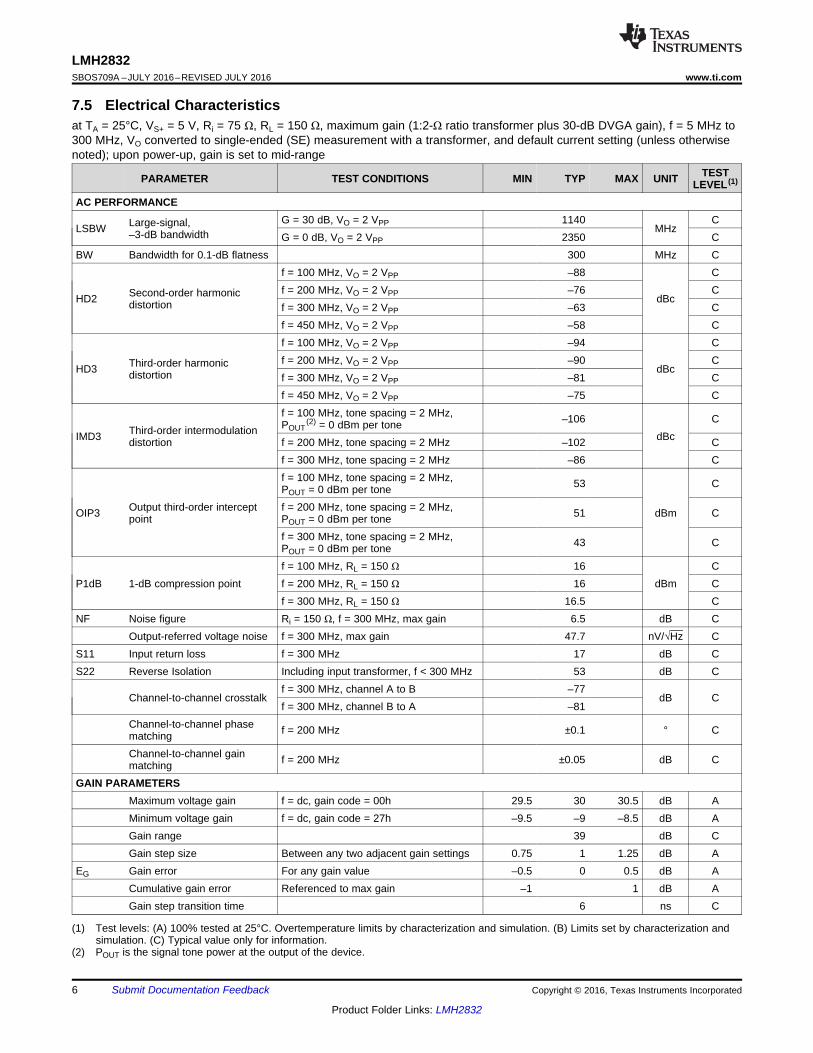
7.5 Electrical Characteristicsat TA = 25°C, VS+ = 5 V, Ri = 75 Ω, RL = 150 Ω, maximum gain (1:2-Ω ratio transformer plus 30-dB DVGA gain), f = 5 MHz to300 MHz, VO converted to single-ended (SE) measurement with a transformer, and default current setting (unless otherwisenoted); upon power-up, gain is set to mid-range
PARAMETER TEST CONDITIONS MIN TYP MAX UNIT TESTLEVEL (1)
AC PERFORMANCE
LSBW Large-signal,–3-dB bandwidth
G = 30 dB, VO = 2 VPP 1140MHz
CG = 0 dB, VO = 2 VPP 2350 C
BW Bandwidth for 0.1-dB flatness 300 MHz C
HD2 Second-order harmonicdistortion
f = 100 MHz, VO = 2 VPP –88
dBc
Cf = 200 MHz, VO = 2 VPP –76 Cf = 300 MHz, VO = 2 VPP –63 Cf = 450 MHz, VO = 2 VPP –58 C
HD3 Third-order harmonicdistortion
f = 100 MHz, VO = 2 VPP –94
dBc
Cf = 200 MHz, VO = 2 VPP –90 Cf = 300 MHz, VO = 2 VPP –81 Cf = 450 MHz, VO = 2 VPP –75 C
IMD3 Third-order intermodulationdistortion
f = 100 MHz, tone spacing = 2 MHz,POUT
(2) = 0 dBm per tone –106dBc
C
f = 200 MHz, tone spacing = 2 MHz –102 Cf = 300 MHz, tone spacing = 2 MHz –86 C
OIP3 Output third-order interceptpoint
f = 100 MHz, tone spacing = 2 MHz,POUT = 0 dBm per tone 53
dBm
C
f = 200 MHz, tone spacing = 2 MHz,POUT = 0 dBm per tone 51 C
f = 300 MHz, tone spacing = 2 MHz,POUT = 0 dBm per tone 43 C
P1dB 1-dB compression pointf = 100 MHz, RL = 150 Ω 16
dBmC
f = 200 MHz, RL = 150 Ω 16 Cf = 300 MHz, RL = 150 Ω 16.5 C
NF Noise figure Ri = 150 Ω, f = 300 MHz, max gain 6.5 dB COutput-referred voltage noise f = 300 MHz, max gain 47.7 nV/√Hz C
S11 Input return loss f = 300 MHz 17 dB CS22 Reverse Isolation Including input transformer, f < 300 MHz 53 dB C
Channel-to-channel crosstalkf = 300 MHz, channel A to B –77
dB Cf = 300 MHz, channel B to A –81
Channel-to-channel phasematching f = 200 MHz ±0.1 ° C
Channel-to-channel gainmatching f = 200 MHz ±0.05 dB C
GAIN PARAMETERSMaximum voltage gain f = dc, gain code = 00h 29.5 30 30.5 dB AMinimum voltage gain f = dc, gain code = 27h –9.5 –9 –8.5 dB AGain range 39 dB CGain step size Between any two adjacent gain settings 0.75 1 1.25 dB A
EG Gain error For any gain value –0.5 0 0.5 dB ACumulative gain error Referenced to max gain –1 1 dB AGain step transition time 6 ns C

7
LMH2832www.ti.com SBOS709A –JULY 2016–REVISED JULY 2016
Product Folder Links: LMH2832
Submit Documentation FeedbackCopyright © 2016, Texas Instruments Incorporated
Electrical Characteristics (continued)at TA = 25°C, VS+ = 5 V, Ri = 75 Ω, RL = 150 Ω, maximum gain (1:2-Ω ratio transformer plus 30-dB DVGA gain), f = 5 MHz to300 MHz, VO converted to single-ended (SE) measurement with a transformer, and default current setting (unless otherwisenoted); upon power-up, gain is set to mid-range
PARAMETER TEST CONDITIONS MIN TYP MAX UNIT TESTLEVEL (1)
(3) PSRR is defined with respect to a differential output.(4) The device power-down function can be controlled by the PDx pins or by the power-down register accessible from the SPI interface.
ANALOG INPUT CHARACTERISTICSzin Input resistance f = dc, differential 135 150 165 Ω ACin Input capacitance Differential 0.6 pF C
Single-ended input resistance f = dc 67.5 75 82.5 Ω ASingle-ended inputcapacitance 1.2 pF C
VICM Input common-mode voltage Internally biased to mid-supply –0.2 0.2 V AVIL Low-level input voltage range Differential gain shift < 1 dB (VS–) + 1.5 V CVIH High-level input voltage range Differential gain shift < 1 dB (VS+) – 1.5 V CANALOG OUTPUT CHARACTERISTICSzo Output resistance Differential 20 Ω C
VOLLow-level output voltagerange VS = 5 V, GND = 0 V 1.15 1.25 V A
VOHHigh-level output voltagerange VS = 5 V, GND = 0 V 3.75 3.85 V A
VOMMaximum output voltageswing
TA = 25°C 5 5.4V
ATA = –40°C to +85°C 5.4 6.4 B
CMRR Common-mode rejection ratio 56 dB CPOWER SUPPLYVS Supply voltage 4.75 5.0 5.25 V A
IQ Quiescent current per channelDefault current, default bias setting 102 105 108
mAA
Min current, lowest power setting 90 CMax current, highest bias setting 108 C
±PSRR Power-supply rejection ratio (3) Gain = 30 dB –48 dB CPOWER-DOWN (4)
Power-down quiescent current(per channel)
TA = 25°C 2.5 6mA
ATA = –40°C to +85°C 6.5 B
Power-down bias current –2 –1 µA A
Turn-on time delay Time to VO = 90% of final value,gain = 0 dB, VI = 2 V 55 ns C
Turn-off time delay Time to VO = 10% of original value,gain = 0 dB, VI = 2 V 110 ns C
Forward isolation in PD mode f = 300 MHz –67 dB CDIGITAL INPUTS/OUTPUTSVIH High-level input voltage 1.4 2 V AVIL Low-level input voltage –0.3 0.8 V A
VOH High-level output voltageIOH = –100 µA 1.65
VA
IOH = –2 mA 1.55 A
VOL Low-level output voltageIOL = 100 µA 0.1
VA
IOL = 2 mA 0.2 A

8
LMH2832SBOS709A –JULY 2016–REVISED JULY 2016 www.ti.com
Product Folder Links: LMH2832
Submit Documentation Feedback Copyright © 2016, Texas Instruments Incorporated
(1) Tested on the automated test equipment (ATE) only up to 25 MHz.(2) Referenced to the negative edge of SCLK.(3) Referenced to the positive edge of SCLK.
7.6 Timing Requirements: SPIMIN TYP MAX UNIT
fS_C SCLK frequency (1) 0 25 50 MHztPH SCLK pulse duration, high 10 nstPL SCLK pulse duration, low 10 nstSU SDI setup 3 nstH SDO hold 3 nstIZ SDO tri-state 3 nstODZ SDO driven to tri-state (2) 0 10 20 nstOZD SDO tri-state to driven 0 2 5 nstOD SDO output delay (2) 0 10 12 nstCSS CS setup (3) 3 5 nstCSH CS hold 3 nstIAG Inter-access gap 20 ns
Frequency (MHz)
OIP
3 (d
Bm
)
0 50 100 150 200 250 300 350 400 450 500 550 60025
30
35
40
45
50
55
60
D002
Av = 30 dBAv = 22 dBAv = 14 dBAv = 6 dBAv = 2 dBAv = -2 dB
Frequency (MHz)
OIP
3 (d
Bm
)
0 50 100 150 200 250 300 350 400 450 500 550 60025
30
35
40
45
50
55
60
D004
-40'C27'C90'C105'C
Frequency (MHz)
Inpu
t Ret
urn
Loss
(dB
)
1 10 100 1000 3000-60
-55
-50
-45
-40
-35
-30
-25
-20
-15
-10
-5
0
D008Voltage Gain (dB)
Gai
n M
atch
ing
Err
or (
dB)
Pha
se M
atch
ing
Err
or (q)
-9 -6 -3 0 3 6 9 12 15 18 21 24 27 30-0.1 -0.2
-0.05 -0.1
0 0
0.05 0.1
0.1 0.2
D034
Gain Matching Error (dB)Phase Matching Error (°)
Frequency (MHz)
Vol
tage
Gai
n (d
B)
1 10 100 1000 80008000-16
-12
-8
-4
0
4
8
12
16
20
24
28
32
D001Temperature (°C)
Gai
n (d
B)
-40 -20 0 20 40 60 80 100 11028.8
29
29.2
29.4
29.6
29.8
30
30.2
30.4
30.6
30.8
31
D025
f = 50 MHzf = 100 MHzf = 200 MHzf = 300 MHzf = 400 MHzf = 500 MHz
9
LMH2832www.ti.com SBOS709A –JULY 2016–REVISED JULY 2016
Product Folder Links: LMH2832
Submit Documentation FeedbackCopyright © 2016, Texas Instruments Incorporated
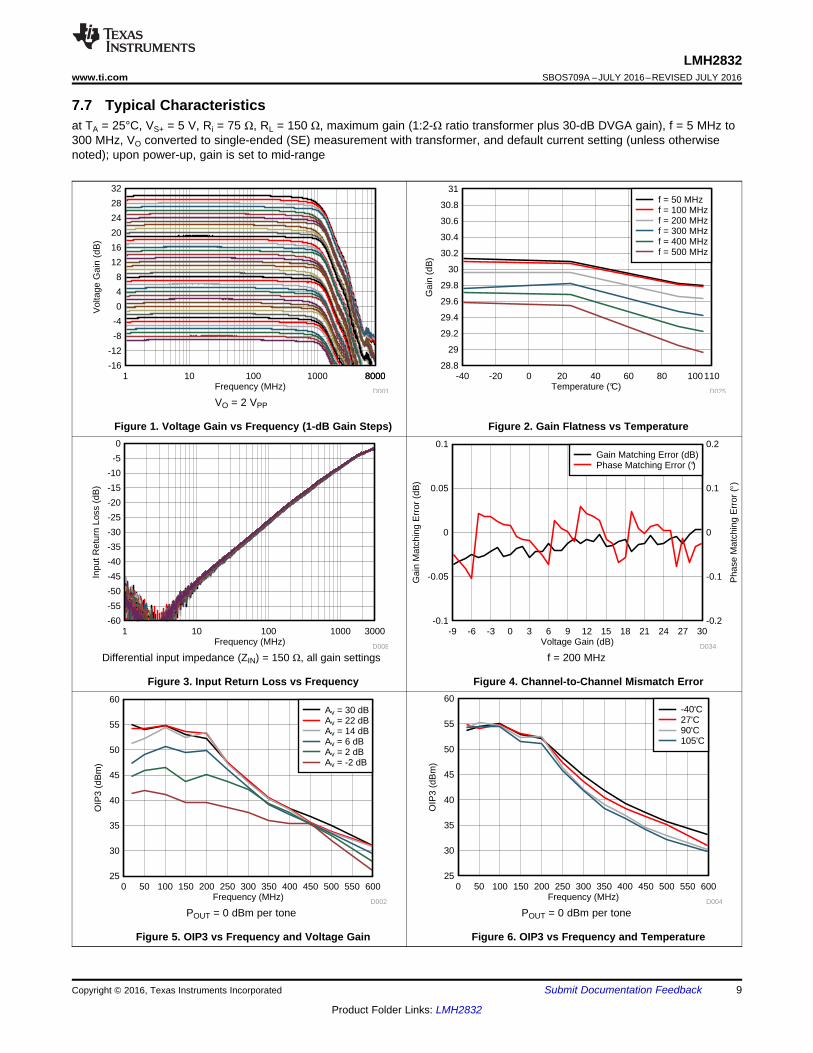
7.7 Typical Characteristicsat TA = 25°C, VS+ = 5 V, Ri = 75 Ω, RL = 150 Ω, maximum gain (1:2-Ω ratio transformer plus 30-dB DVGA gain), f = 5 MHz to300 MHz, VO converted to single-ended (SE) measurement with transformer, and default current setting (unless otherwisenoted); upon power-up, gain is set to mid-range
VO = 2 VPP
Figure 1. Voltage Gain vs Frequency (1-dB Gain Steps) Figure 2. Gain Flatness vs Temperature
Differential input impedance (ZIN) = 150 Ω, all gain settings
Figure 3. Input Return Loss vs Frequency
f = 200 MHz
Figure 4. Channel-to-Channel Mismatch Error
POUT = 0 dBm per tone
Figure 5. OIP3 vs Frequency and Voltage Gain
POUT = 0 dBm per tone
Figure 6. OIP3 vs Frequency and Temperature

Temperature (°C)
OIP
3 (d
Bm
)
-40 -20 0 20 40 60 80 100 11046
47
48
49
50
51
52
53
54
55
56
D038
Bias Setting = 00hBias Setting = 02hBias Setting = 08hBias Setting = 20hBias Setting = 80h
Frequency (MHz)
Inte
rmod
ulat
ion
Dis
tort
ion
(dB
c)
0 50 100 150 200 250 300 350 400 450 500-120
-110
-100
-90
-80
-70
-60
-50
-40
-30
-20
-10
0
D039
IMD2 (dBc)IMD3 (dBc)
Temperature (°C)
OIP
3 (d
Bm
)
-40 -20 0 20 40 60 80 100 11050
51
52
53
54
55
56
57
58
D006
VS = 4.5 VVS = 4.75 VVS = 5 VVS = 5.25 V
Temperature (°C)
OIP
3 (d
Bm
)
-40 -20 0 20 40 60 80 100 11040
41
42
43
44
45
46
D007
VS = 4.5 VVS = 4.75 VVS = 5 VVS = 5.25 V
POUT per tone (dBm)
OIP
3 (d
Bm
)
0 2 4 6 8 10 12 1425
30
35
40
45
50
55
60
D003
Av = 30 dBAv = 22 dBAv = 14 dBAv = 6 dBAv = 2 dBAv = -2 dB
Frequency (MHz)
OIP
3 (d
Bm
)
0 50 100 150 200 250 300 350 400 450 500 550 60025
30
35
40
45
50
55
60
D005
Channel AChannel B
10
LMH2832SBOS709A –JULY 2016–REVISED JULY 2016 www.ti.com
Product Folder Links: LMH2832
Submit Documentation Feedback Copyright © 2016, Texas Instruments Incorporated
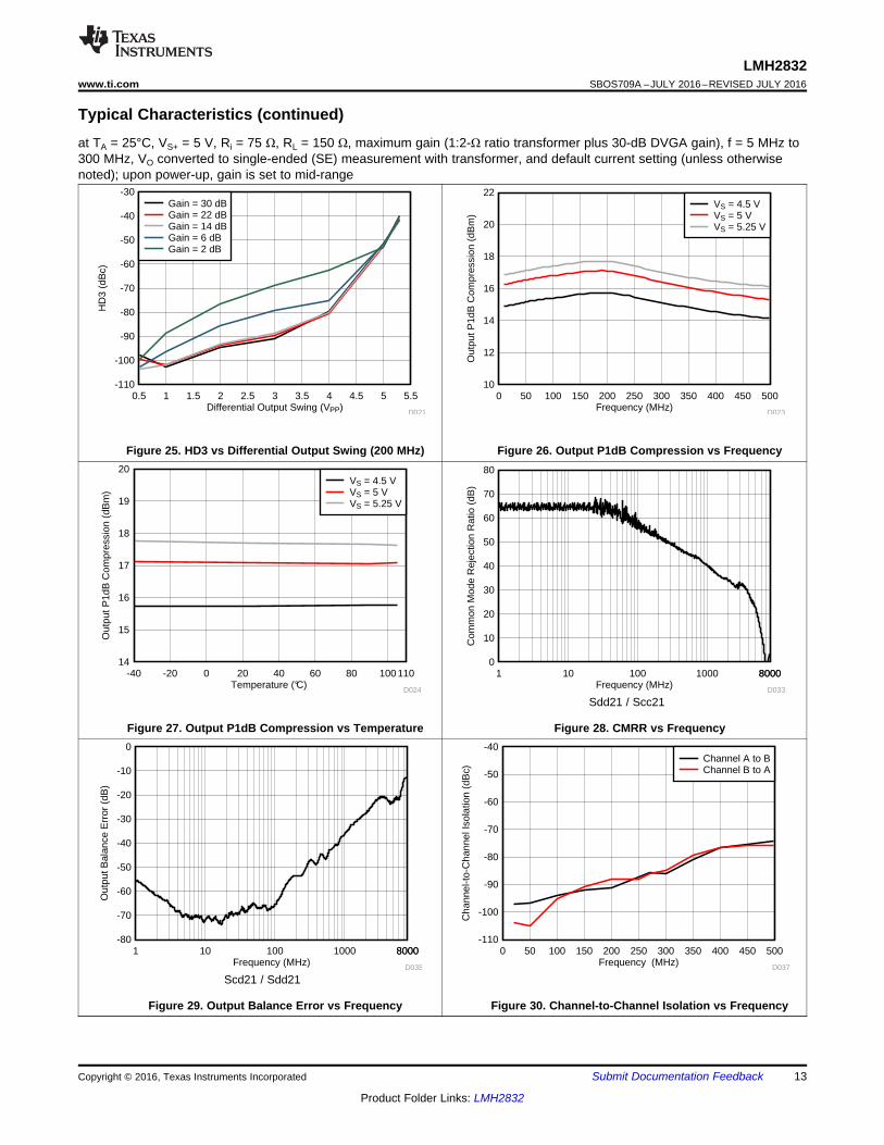
Typical Characteristics (continued)at TA = 25°C, VS+ = 5 V, Ri = 75 Ω, RL = 150 Ω, maximum gain (1:2-Ω ratio transformer plus 30-dB DVGA gain), f = 5 MHz to300 MHz, VO converted to single-ended (SE) measurement with transformer, and default current setting (unless otherwisenoted); upon power-up, gain is set to mid-range
f = 200 MHz
Figure 7. OIP3 vs Output Power
POUT = 0 dBm per tone
Figure 8. OIP3 Channel Comparison
POUT = 0 dBm per tone
Figure 9. OIP3 vs Temperature and Supply Voltage(f = 200 MHz)
POUT = 0 dBm per tone
Figure 10. OIP3 vs Temperature and Supply Voltage(f = 300 MHz)
POUT = 0 dBm per tone
Figure 11. OIP3 vs Temperature and Bias Setting(f = 200 MHz)
POUT = 0 dBm per tone
Figure 12. Intermodulation Distortion vs Frequency

Frequency (MHz)
HD
2 (d
Bc)
0 50 100 150 200 250 300 350 400 450 500-100
-90
-80
-70
-60
-50
-40
-30
-20
-10
0
D014
-40°C25°C90°C105°C
Frequency (MHz)
HD
3 (d
Bc)
0 50 100 150 200 250 300 350 400 450 500-120
-110
-100
-90
-80
-70
-60
-50
-40
-30
-20
-10
0
D015
-40°C25°C90°C105°C
Frequency (MHz)
HD
2 (d
Bc)
0 50 100 150 200 250 300 350 400 450 500-100
-90
-80
-70
-60
-50
-40
-30
-20
-10
0
D012
Gain = 30 dBGain = 22 dBGain = 14 dBGain = 6 dBGain = 2 dBGain = -2 dB
Frequency (MHz)
HD
3 (d
Bc)
0 50 100 150 200 250 300 350 400 450 500-120
-110
-100
-90
-80
-70
-60
-50
-40
-30
-20
-10
0
D013
Gain = 30 dBGain = 22 dBGain = 14 dBGain = 6 dBGain = 2 dBGain = -2 dB
Voltage Gain (dB)
Noi
se F
igur
e (d
B)
-9 -6 -3 0 3 6 9 12 15 18 21 24 27 305
10
15
20
25
30
35
40
45
50
D011
f = 50 MHzf = 100 MHzf = 200 MHzf = 300 MHz
Frequency (MHz)
Noi
se F
igur
e (d
B)
0 50 100 150 200 250 300 350 400 450 5004
5
6
7
8
9
10
11
12
D022
25°C
11
LMH2832www.ti.com SBOS709A –JULY 2016–REVISED JULY 2016
Product Folder Links: LMH2832
Submit Documentation FeedbackCopyright © 2016, Texas Instruments Incorporated
Typical Characteristics (continued)at TA = 25°C, VS+ = 5 V, Ri = 75 Ω, RL = 150 Ω, maximum gain (1:2-Ω ratio transformer plus 30-dB DVGA gain), f = 5 MHz to300 MHz, VO converted to single-ended (SE) measurement with transformer, and default current setting (unless otherwisenoted); upon power-up, gain is set to mid-range
ZIN = 150 Ω
Figure 13. Noise Figure vs Voltage Gain Figure 14. Noise Figure vs Frequency
VO = 2 VPP
Figure 15. HD2 vs Frequency and Gain Settings
VO = 2 VPP
Figure 16. HD3 vs Frequency and Gain Settings
VO = 2 VPP
Figure 17. HD2 vs Frequency and Temperature
VO = 2 VPP
Figure 18. HD3 vs Frequency and Temperature

Differential Output Swing (VPP)
HD
3 (d
Bc)
0.5 1 1.5 2 2.5 3 3.5 4 4.5 5 5.5-100
-90
-80
-70
-60
-50
-40
D019
Gain = 30 dBGain = 22 dBGain = 14 dBGain = 6 dBGain = 2 dB
Differential Output Swing (VPP)
HD
2 (d
Bc)
0.5 1 1.5 2 2.5 3 3.5 4 4.5 5 5.5-100
-90
-80
-70
-60
-50
-40
-30
D020
Gain = 30 dBGain = 22 dBGain = 14 dBGain = 6 dBGain = 2 dB
Temperature (°C)
Har
mon
ic D
isto
rtio
n (d
Bc)
-40 -20 0 20 40 60 80 100 110-100
-95
-90
-85
-80
-75
-70
-65
-60
-55
-50
D017
VS = 4.5 V (HD2)VS = 4.5 V (HD3)VS = 5 V (HD2)VS = 5 V (HD3)VS = 5.25 V (HD2)VS = 5.25 V (HD3)
Differential Output Swing (VPP)
HD
2 (d
Bc)
0.5 1 1.5 2 2.5 3 3.5 4 4.5 5 5.5-100
-90
-80
-70
-60
-50
-40
D018
Gain = 30 dBGain = 22 dBGain = 14 dBGain = 6 dBGain = 2 dB
Frequency (MHz)
Har
mon
ic D
isto
rtio
n (d
Bc)
0 50 100 150 200 250 300 350 400 450 500-120
-110
-100
-90
-80
-70
-60
-50
-40
-30
-20
-10
0
D040
Channel A (HD2)Channel A (HD3)Channel B (HD2)Channel B (HD3)
Temperature (°C)
Har
mon
ic D
isto
rtio
n (d
Bc)
-40 -20 0 20 40 60 80 100 110-100
-95
-90
-85
-80
-75
-70
-65
-60
-55
-50
D016
VS = 4.5 V (HD2)VS = 4.5 V (HD3)VS = 5 V (HD2)VS = 5 V (HD3)VS = 5.25 V (HD2)VS = 5.25 V (HD3)
12
LMH2832SBOS709A –JULY 2016–REVISED JULY 2016 www.ti.com
Product Folder Links: LMH2832
Submit Documentation Feedback Copyright © 2016, Texas Instruments Incorporated
Typical Characteristics (continued)at TA = 25°C, VS+ = 5 V, Ri = 75 Ω, RL = 150 Ω, maximum gain (1:2-Ω ratio transformer plus 30-dB DVGA gain), f = 5 MHz to300 MHz, VO converted to single-ended (SE) measurement with transformer, and default current setting (unless otherwisenoted); upon power-up, gain is set to mid-range
Figure 19. Harmonic Distortion Between Channels
VO = 2 VPP
Figure 20. Harmonic Distortion vs Temperature andSupply Voltage (100 MHz)
VO = 2 VPP
Figure 21. Harmonic Distortion vs Temperature andSupply Voltage (200 MHz)
Figure 22. HD2 vs Differential Output Swing (100 MHz)
Figure 23. HD3 vs Differential Output Swing (100 MHz) Figure 24. HD2 vs Differential Output Swing (200 MHz)
Frequency (MHz)
Out
put B
alan
ce E
rror
(dB
)
1 10 100 1000 80008000-80
-70
-60
-50
-40
-30
-20
-10
0
D035Frequency (MHz)
Cha
nnel
-to-
Cha
nnel
Isol
atio
n (d
Bc)
0 50 100 150 200 250 300 350 400 450 500-110
-100
-90
-80
-70
-60
-50
-40
D037
Channel A to BChannel B to A
Temperature (°C)
Out
put P
1dB
Com
pres
sion
(dB
m)
-40 -20 0 20 40 60 80 100 11014
15
16
17
18
19
20
D024
VS = 4.5 VVS = 5 VVS = 5.25 V
Frequency (MHz)
Com
mon
Mod
e R
ejec
tion
Rat
io (
dB)
1 10 100 1000 800080000
10
20
30
40
50
60
70
80
D033
Differential Output Swing (VPP)
HD
3 (d
Bc)
0.5 1 1.5 2 2.5 3 3.5 4 4.5 5 5.5-110
-100
-90
-80
-70
-60
-50
-40
-30
D021
Gain = 30 dBGain = 22 dBGain = 14 dBGain = 6 dBGain = 2 dB
Frequency (MHz)
Out
put P
1dB
Com
pres
sion
(dB
m)
0 50 100 150 200 250 300 350 400 450 50010
12
14
16
18
20
22
D023
VS = 4.5 VVS = 5 VVS = 5.25 V
13
LMH2832www.ti.com SBOS709A –JULY 2016–REVISED JULY 2016
Product Folder Links: LMH2832
Submit Documentation FeedbackCopyright © 2016, Texas Instruments Incorporated
Typical Characteristics (continued)at TA = 25°C, VS+ = 5 V, Ri = 75 Ω, RL = 150 Ω, maximum gain (1:2-Ω ratio transformer plus 30-dB DVGA gain), f = 5 MHz to300 MHz, VO converted to single-ended (SE) measurement with transformer, and default current setting (unless otherwisenoted); upon power-up, gain is set to mid-range
Figure 25. HD3 vs Differential Output Swing (200 MHz) Figure 26. Output P1dB Compression vs Frequency
Figure 27. Output P1dB Compression vs Temperature
Sdd21 / Scc21
Figure 28. CMRR vs Frequency
Scd21 / Sdd21
Figure 29. Output Balance Error vs Frequency Figure 30. Channel-to-Channel Isolation vs Frequency

Time (10 ns/div)
SC
LK (
V)
Out
put (
V)
-1.2 -1.2
-0.8 -0.8
-0.4 -0.4
0 0
0.4 0.4
0.8 0.8
1.2 1.2
1.6 1.6
2 2
2.4 2.4
D027
SCLKOutput
Time (10 ns/div)
SC
LK (
V)
Out
put (
V)
-1.2 -1.2
-0.8 -0.8
-0.4 -0.4
0 0
0.4 0.4
0.8 0.8
1.2 1.2
1.6 1.6
2 2
2.4 2.4
D028
SCLKOutput
Frequency (MHz)
Out
put I
mpe
danc
e (:
)
1 10 100 1000 2000-100
-50
0
50
100
150
200
D036
R (:)jX (:)|Z| (:)
Time (50 ns/div)
Pow
er D
own
Pin
(V
)
Out
put (
V)
-0.4 -1
0 -0.5
0.4 0
0.8 0.5
1.2 1
1.6 1.5
2 2
2.4 2.5
D026
Power Down PinOutput
Voltage Gain (dB)
Cum
ulat
ive
Gai
n S
tep
Err
or (
dB)
-9 -6 -3 0 3 6 9 12 15 18 21 24 27 30-0.15
-0.1
-0.05
0
0.05
0.1
0.15
D009
f = 100 MHzf = 200 MHzf = 300 MHz
Voltage Gain (dB)
Cum
ulat
ive
Pha
se S
tep
Err
or (
dB)
-9 -6 -3 0 3 6 9 12 15 18 21 24 27 30-6
-4
-2
0
2
4
6
D010
f = 100 MHzf = 200 MHzf = 300 MHz
14
LMH2832SBOS709A –JULY 2016–REVISED JULY 2016 www.ti.com
Product Folder Links: LMH2832
Submit Documentation Feedback Copyright © 2016, Texas Instruments Incorporated
Typical Characteristics (continued)at TA = 25°C, VS+ = 5 V, Ri = 75 Ω, RL = 150 Ω, maximum gain (1:2-Ω ratio transformer plus 30-dB DVGA gain), f = 5 MHz to300 MHz, VO converted to single-ended (SE) measurement with transformer, and default current setting (unless otherwisenoted); upon power-up, gain is set to mid-range
Figure 31. Cumulative Gain Step Error vs Voltage Gain Figure 32. Cumulative Phase Step Error vs Voltage Gain
Figure 33. Output Impedance vs Frequency Figure 34. Power-Down Transition Response
Figure 35. Gain Switching Response (AV = 30 dB to 22 dB) Figure 36. Gain Switching Response (AV = 22 dB to 30 dB)

Time (10 ns/div)
SC
LK (
V)
Out
put (
V)
-1.2 -1.2
-0.8 -0.8
-0.4 -0.4
0 0
0.4 0.4
0.8 0.8
1.2 1.2
1.6 1.6
2 2
2.4 2.4
D031
SCLKOutput
Time (10 ns/div)
SC
LK (
V)
Out
put (
V)
-1.2 -1.2
-0.8 -0.8
-0.4 -0.4
0 0
0.4 0.4
0.8 0.8
1.2 1.2
1.6 1.6
2 2
2.4 2.4
D032
SCLKOutput
Time (10 ns/div)
SC
LK (
V)
Out
put (
V)
-1.2 -1.2
-0.8 -0.8
-0.4 -0.4
0 0
0.4 0.4
0.8 0.8
1.2 1.2
1.6 1.6
2 2
2.4 2.4
D029
SCLKOutput
Time (10 ns/div)
SC
LK (
V)
Out
put (
V)
-1.2 -1.2
-0.8 -0.8
-0.4 -0.4
0 0
0.4 0.4
0.8 0.8
1.2 1.2
1.6 1.6
2 2
2.4 2.4
D030
SCLKOutput
15
LMH2832www.ti.com SBOS709A –JULY 2016–REVISED JULY 2016
Product Folder Links: LMH2832
Submit Documentation FeedbackCopyright © 2016, Texas Instruments Incorporated
Typical Characteristics (continued)at TA = 25°C, VS+ = 5 V, Ri = 75 Ω, RL = 150 Ω, maximum gain (1:2-Ω ratio transformer plus 30-dB DVGA gain), f = 5 MHz to300 MHz, VO converted to single-ended (SE) measurement with transformer, and default current setting (unless otherwisenoted); upon power-up, gain is set to mid-range
Figure 37. Gain Switching Response (AV = 30 dB to 14 dB) Figure 38. Gain Switching Response (AV = 14 dB to 30 dB)
Figure 39. Gain Switching Response (AV = 30 dB to 6 dB) Figure 40. Gain Switching Response (AV = 6 dB to 30 dB)

10
10
½ LMH2832
INPx
INMx
OUTPx
OUTMx
Copyright © 2016, Texas Instruments Incorporated
40
40
USB
SPI
VS+ = 5 V
GND
LMH2832EVM-75
0.1 µF
0.1 µF
0.1 µF
0.1 µF
50
Spectrum Analyzer with 50-,QSXWV
ETC1-1-13T(1:1, zo = 50 )
BMP5075
F-Connector
SMA
50-5HIHUHQFH
75-5HIHUHQFH
MABA011033(1:2, zo = 75 )
50
Signal Generator with 50-2XWSXWV
Band-PassFilter
50
Signal Generator with 50-2XWSXWV
ZFSCJ-2-1 or
ZFSCJ-2-4
6-dB Attenuation
Pads OUT_AMP+-
10-
10-
½ LMH2832
INPx
INMx
OUTPx
OUTMx
40
40
USB
SPI
VS+ = 5 V
GND
LMH2832EVM-75
0.1 µF
0.1 µF
0.1 µF
0.1 µF
50
Spectrum Analyzer with 50-,QSXWV
ETC1-1-13T(1:1, zo = 50 )
BMP5075
BMP5075
50
Signal Generatorwith 50-2XWSXWV
zo = 50 , 1:2
0º
180º
Band-PassFilter ZFSCJ-2-1-S+
F-Connector
F-Connector
SMA
50-5HIHUHQFH 75-5HIHUHQFH
OUT_AMP+-
Copyright © 2016, Texas Instruments Incorporated
10
10
½ LMH2832
INPx
INMx
OUTPx
OUTMx
15
15
USB
SPI
VS+ = 5 V
GND
LMH2832EVM-50
50
50
Port 2
Port 4
Test Equipment with 50-,QSXWV/Outputs
50
50 Port 1
Port 3
Test Equipment with 50-,QSXWV/Outputs
Vector Network Analyzer
Vector Network Analyzer
0.1 µF
0.1 µF
0.1 µF
0.1 µFSMA
SMA
SMA
SMA
OUT_AMP+- OUT_LOAD
+-
Copyright © 2016, Texas Instruments Incorporated
16
LMH2832SBOS709A –JULY 2016–REVISED JULY 2016 www.ti.com
Product Folder Links: LMH2832
Submit Documentation Feedback Copyright © 2016, Texas Instruments Incorporated
8 Parameter Measurement Information
8.1 Setup DiagramsFigure 41 to Figure 44 illustrate various test setup diagrams using the LMH2832 evaluation module (EVM).
Figure 41. Frequency Response Differential Test Setup
Figure 42. Single-Tone Harmonic Distortion Test Setup
Figure 43. Two-Tone Linearity Test Setup (OIP3, OIP2)

10
10
½ LMH2832
INPx
INMx
OUTPx
OUTMx
40
40
USB
SPI
VS+ = 5 V
GND
LMH2832EVM-50
0.1 µF
0.1 µF
0.1 µF
0.1 µF
ETC1-1-13T(1:1, zo = 50 )
SMA
MABA011038(1:3, zo = 50 )
SMA
50
Agilent E4443A with 50-2XWSXWV
346B Noise Source
50
Agilent E4443A with 50-,QSXWV
Copyright © 2016, Texas Instruments Incorporated
17
LMH2832www.ti.com SBOS709A –JULY 2016–REVISED JULY 2016
Product Folder Links: LMH2832
Submit Documentation FeedbackCopyright © 2016, Texas Instruments Incorporated
Setup Diagrams (continued)
Figure 44. Noise Figure Test Setup
8.2 ATE Testing and DC MeasurementsAll production testing and dc parameters are measured on automated test equipment (ATE) capable of dcmeasurements only. Some measurements (such as voltage gain) are referenced to the output of the internalamplifier and do not include losses attributed to the on-chip output resistors. The Electrical Characteristics valuesspecify these conditions. When the measurement is referred to the amplifier output, the output resistors are notincluded in the measurement. If the measurement is referred to the device pins, then the output resistor loss isincluded in the measurement.
8.3 Frequency ResponseThis test is done by running an S-parameter sweep on a 4-port differential network analyzer using the standardEVM with no baluns; see Figure 41. The inputs and outputs of the EVM are connected to the network analyzerusing 75-Ω coaxial cables with the input ports set to a characteristic impedance of 75 Ω, and the output ports setto a characteristic impedance of 50 Ω.
The frequency response test with capacitive load is done by soldering the capacitor across the LMH2832 outputpins. In this configuration, the on-chip, 10-Ω resistors on each output leg isolate the capacitive load from theamplifier output pins.
8.4 DistortionThe standard EVM is used for measuring both the single-tone harmonic distortion and two-tone intermodulationdistortion; see Figure 42 and Figure 43, respectively. The distortion is measured with differential input signals tothe LMH2832. In order to interface with 50-Ω, single-ended test equipment, 50-Ω to 75-Ω impedance matchingpads followed by external baluns (1:2, zo = 75 Ω) are required between the EVM output ports and the testequipment. These baluns are used to combine two single tones in the two-tone test plots as well as to convertthe single-ended input to differential output for harmonic distortion tests. The use of 6-dB attenuator pads on boththe inputs and outputs is recommended to provide a balanced match between the external balun and the EVM.
8.5 Noise FigureThis test is done by matching the input of the LMH2832 to a 50-Ω noise source using a 50-Ω to 75-Ω impedancetransformation pad followed by a 1:2 balun (Figure 44), with the noise figure being referred to the inputimpedance (RS = 150 Ω). As noted in Figure 44, a Keysight Technologies™ E4443A with NF features is used forthe testing.

18
LMH2832SBOS709A –JULY 2016–REVISED JULY 2016 www.ti.com
Product Folder Links: LMH2832
Submit Documentation Feedback Copyright © 2016, Texas Instruments Incorporated
8.6 Pulse Response, Slew Rate, and Overdrive RecoveryFor time-domain measurements, the standard EVM is driven through an impedance transformation pad and abalun again to convert a single-ended output from the test equipment to the differential inputs of the LMH2832.The differential outputs are directly connected to the oscilloscope inputs, with the differential signal responsecalculated using trace math from the two separate oscilloscope inputs.
8.7 Power-DownThe standard EVM is used for this test by completely removing the shorting block on jumper JPD. A high-speed,50-Ω pulse generator is used to drive the PDx pin that toggles the output signal on or off depending upon thePDx pin voltage.
8.8 Crosstalk, Gain Matching, and Phase MatchingThe standard EVM is used for these tests with both channels enabled. For gain and phase matching, theresponses of both channels are measured on a network analyzer and the gain and phase values are compared.For crosstalk, a single channel is driven with a signal on the network analyzer when the other channel ismeasured.
8.9 Output Measurement Reference PointsThe LMH2832 has two on-chip, 10-Ω output resistors on each channel. When matching the output to a 100-Ωload, the evaluation module (EVM) uses an external 40-Ω resistor on each output leg to complete the outputmatching. The inclusion of on-chip output resistors creates two potential reference points for measuring theoutput voltage. The first reference point is at the internal amplifier output (OUT_AMP), and the second referencepoint is at the externally-matched 100-Ω load (OUT_LOAD). The measurements in the Electrical Characteristicstable and in the Typical Characteristics section are referred to the (OUT_AMP) reference point unless otherwisespecified. The conversion between reference points is a straightforward correction of 3 dB for power and 6 dB forvoltage, as shown in Equation 1 and Equation 2. The measurements are referenced to OUT_AMP when notspecified.
VOUT_LOAD = (VOUT_AMP – 6 dB) (1)POUT_LOAD = (POUT_AMP – 3 dB) (2)

INPA
INMA
PDA
SCLKSDI
SDO
PDB
INMB
INPB
SPI POR
Channel A Control Logic
Channel B Control Logic
FDAG = 30 dB
FDAG = 30 dB
OUTPA
OUTMA
OUTMB
OUTPB
1-dB Attenuator Steps:0 dB to -39 dB
1-dB Attenuator Steps:0 dB to -39 dB
150
150
CS
19
LMH2832www.ti.com SBOS709A –JULY 2016–REVISED JULY 2016
Product Folder Links: LMH2832
Submit Documentation FeedbackCopyright © 2016, Texas Instruments Incorporated
9 Detailed Description
9.1 OverviewEach channel of the LMH2832 consists of an input attenuator block followed by a fully differential amplifier thathas a gain of 30 dB. The attenuator has a range of 0 dB to –39 dB in 1-dB steps that is controlled by an SPIinterface. The two channels can be controlled independently using the digital interface including power-down andbias settings. A separate analog power-down pin (PDA, PDB) is also included for each channel so that thedevice can bet set to a low-power state without waiting for a serial write to a register. The internal registers alsoinclude a power-on-reset (POR) that ensures the device starts in a known state after the power is reset.
9.2 Functional Block Diagram
9.3 Feature Description
9.3.1 Analog Input CharacteristicsThe LMH2832 is a dual-channel device with two identical channels (A and B) that each have differential inputpins (INP and INM) that denote the positive and negative inputs, respectively. The inputs are expected to be ac-coupled only, typically through a transformer or capacitor. The amplifier self-biases the input common-mode tomid-supply for the maximum input voltage range. The inputs of the LMH2832 can only be driven differentially. Forsingle-ended input source applications, use a balun or fully differential amplifier (such as the LMH3401 orLMH5401) that can convert single-ended to differential signals before the LMH2832.

20
LMH2832SBOS709A –JULY 2016–REVISED JULY 2016 www.ti.com
Product Folder Links: LMH2832
Submit Documentation Feedback Copyright © 2016, Texas Instruments Incorporated
Feature Description (continued)At maximum gain, the digital attenuator is set to 0 dB of attenuation, causing the input signal to be much largerthan the output signal and forcing the maximum output voltage swing to be limited by the outputs of the device.However at minimum gain, the maximum voltage swing is limited by the inputs of the device because theattenuator causes the output voltage to be 9 dB lower than the input voltage. In minimum gain, the input voltagelimits against the electrostatic discharge (ESD) devices before the output reaches the maximum swing limits. Forlinear operation, the input voltage must be kept within the maximum input voltage ratings described in theElectrical Characteristics table.
The input impedance of the LMH2832 is set by internal termination resistors to a nominal value of 150 Ω,differential. Process variations result in a range of values, as described in the Electrical Characteristics table. Theinput impedance is also affected by device parasitic effects at higher frequencies that cause the impedance toshift away from the nominal value.
9.3.2 Analog Output CharacteristicsThe LMH2832 has series, 10-Ω, on-chip resistors on each output to provide isolation from board parasitics thatcan cause instability. When designing a filter following the LMH2832, the filter source impedance calculationmust include the two 10-Ω, on-chip resistors. Table 2 shows the calculated external source impedance valuesrequired for various matched filter loads.
Table 2. Output Resistor Values for Matched LoadsMATCHED FILTER IMPEDANCE (Ω) EXTERNAL SERIES RESISTOR PER OUTPUT (Ω)
100 80150 130200 180300 280
9.3.3 Driving Low Insertion-Loss FiltersWhen driving high-speed ADCs, a filter is commonly driven with a matched impedance to the ADC. Thisimpedance is matched by the amplifier by setting the combination of the output resistors to the same impedanceas the ADC inputs. Impedance matching is often done to minimize any transmission reflections caused by thephysical signal path. The drawback to using a matched impedance is that a voltage swing is required from theamplifier outputs that is twice the desired ADC input voltage swing, which can cause output voltage limitationissues.
To avoid using a matched impedance, a low insertion loss filter can be driven where there is little to noresistance added at the amplifier outputs. The amplifier outputs then only must swing to the value of the ADCfull-scale input voltage, thus eliminating most of the potential amplifier output headroom issues. The requirementsof this technique are that the amplifier must be able to provide enough current to the load of the ADC and thatthe path between the amplifier outputs and ADC inputs must be minimized to prevent any reflections.
9.3.4 Input Impedance MatchingThe LMH2832 has a differential input impedance of 150 Ω that can be easily matched to single-ended, 50-Ω or75-Ω systems using baluns. For a single-ended, 50-Ω input, a 1:3-Ω ratio balun can be used to create a 150-Ωdifferential source impedance to the device with a balun gain of 4.8 dB. For a single-ended, 75-Ω input, a 1:2-Ωratio balun creates a 150-Ω differential source impedance to the device with a voltage gain of 3 dB.
9.3.5 Power-On Reset (POR)The LMH2832 has a built-in, power-on-reset (POR) that sets the device registers to their default state (see theRegister Maps section) on power-up. Note that the LMH2832 register information is lost when power is removed.When power is reapplied, the POR ensures that the device enters a default state. Power glitches (of sufficientduration) can also initiate the POR and return the device to a default state.

21
LMH2832www.ti.com SBOS709A –JULY 2016–REVISED JULY 2016
Product Folder Links: LMH2832
Submit Documentation FeedbackCopyright © 2016, Texas Instruments Incorporated
9.4 Device Functional Modes
9.4.1 Power-Down (PD)The device supports power-down control using an external power-down (PDx) pin or by writing a logic high to bit6 of SPI register 2h (see the Register Maps section). The external PDx pins are active high; when left floating,the device defaults to an on condition resulting from the internal pulldown resistors that cause a logic low on thePDx pins. The device PDx thresholds are noted in the Electrical Characteristics table. The device consumesapproximately 7 mA in power-down mode. Note that the SPI register contents are preserved in power-downmode.
9.4.2 Gain ControlThe LMH2832 gain can be controlled from 30-dB gain (0-dB attenuation) to –9-dB gain in 1-dB steps by digitallyprogramming the SPI register 2h; see the Register Maps section for more details.
9.5 Programming
9.5.1 Details of the Serial InterfaceThe LMH2832 has a set of internal registers that can be accessed by the serial interface formed by the CS(serial interface enable), SCLK (serial interface clock), SDI (serial interface input data), and SDO (serial interfaceread-back data) pins. Serially shifting bits into the device is enabled when CS is low. SDI serial data are latchedat every SCLK rising edge when CS is active (low). The serial data are loaded into the register at every 16thSCLK rising edge when CS is low. When the word length exceeds a multiple of 16 bits, the excess bits areignored. Data can be loaded in multiples of 16-bit words within a single active CS pulse. The first eight bits formthe register address and the remaining eight bits are the register data. The interface can function with SCLKfrequencies from 25 MHz down to very low speeds (of a few hertz) and also with a non-50% SCLK duty cycle. Asummary of the LMH2832 SPI protocol is:1. SPI-1.1 interface2. Independent channel A, B attenuation programming (6-bit gain control)3. SPI register contents are preserved in power-down mode4. SPI-controlled power modes (3-bit control for eight options to step down the power)5. Powered for the main 5-V power supply6. 1.8-V logic

tPL
SCLK
tPH
tPL
CS
SDI
SDO
A6 A5 A4 A3 A2 A1 A0
1 765432 8 9 151413121110 16 17 232221201918 24
SCLK
Addr N Addr N+1
D7 D1D2D3D4D5D6 D0 D7 D1D2D3D4D5D6 D0
CS
SDI
SDO
A6 A5 A4 A3 A2 A1 A0 D7 D1D2D3D4D5D6 D0
1 765432 8 9 151413121110 16 17 232221201918 24
D7 D1D2D3D4D5D6 D0
SCLK
Addr N Addr N+1
CS
SCLK
SDI
SDO
A6 A5 A4 A3 A2 A1 A0
1 765432 8 9 151413121110 16
D7 D1D2D3D4D5D6 D0
CS
SCLK
SDI
SDO
A6 A5 A4 A3 A2 A1 A0 D7 D1D2D3D4D5D6 D0
1 765432 8 9 151413121110 16
22
LMH2832SBOS709A –JULY 2016–REVISED JULY 2016 www.ti.com
Product Folder Links: LMH2832
Submit Documentation Feedback Copyright © 2016, Texas Instruments Incorporated
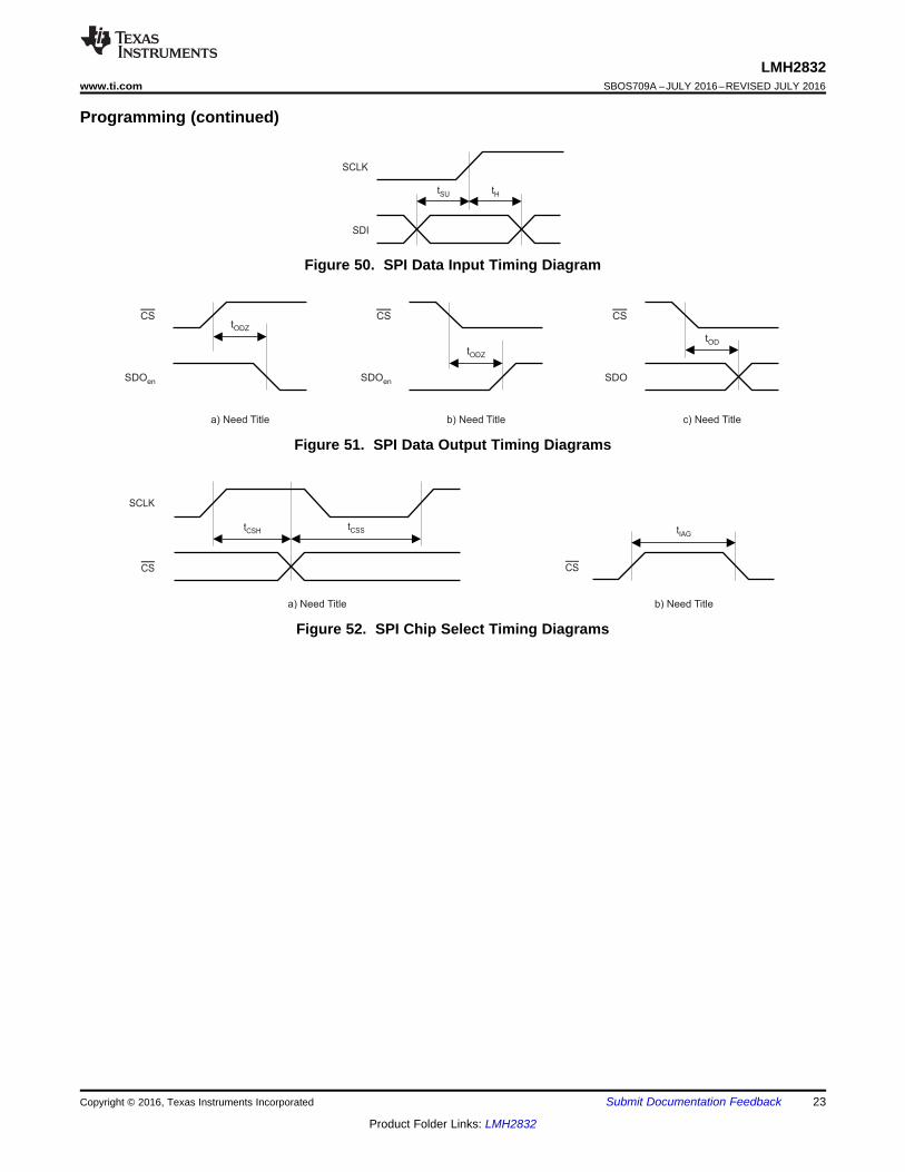
Programming (continued)9.5.2 Timing DiagramsFigure 45 and Figure 46 show timing diagrams for the SPI write and read bus cycles, respectively. Figure 47shows an example timing diagram for a streaming write cycle and Figure 48 shows an example timing diagramfor a streaming read cycle. Figure 49, Figure 50, Figure 51, and Figure 52 illustrate timing diagrams andrequirements for the clock, data input, data output, and chip select, respectively. See the Timing Requirements:SPI table for SPI timing requirements.
Figure 45. SPI Write Bus Cycle Timing Diagram
Figure 46. SPI Read Bus Cycle Timing Diagram
Figure 47. SPI Streaming Write Example Timing Diagram
Figure 48. SPI Streaming Read Example Timing Diagram
Figure 49. SPI Clock Timing Diagram
CS
SCLK
tCSStCSH
CS
tIAG
a) Need Title b) Need Title
SDOen
tODZ
CS
b) Need Title
SDOen
tODZ
CS
a) Need Title
SDO
tOD
CS
c) Need Title
SDI
tSU
SCLK
tH
23
LMH2832www.ti.com SBOS709A –JULY 2016–REVISED JULY 2016
Product Folder Links: LMH2832
Submit Documentation FeedbackCopyright © 2016, Texas Instruments Incorporated
Programming (continued)
Figure 50. SPI Data Input Timing Diagram
Figure 51. SPI Data Output Timing Diagrams
Figure 52. SPI Chip Select Timing Diagrams

LMH2832SBOS709A –JULY 2016–REVISED JULY 2016 www.ti.com
24
Product Folder Links: LMH2832
Submit Documentation Feedback Copyright © 2016, Texas Instruments Incorporated
9.6 Register MapsTable 3 shows the SPI registers for the LMH2832.
Table 3. SPI Register Map
ADDRESS(A[6:0]) R/W
DEFAULT(Hex) REGISTER NAME
REGISTER DATA7 6 5 4 3 2 1 0
0 R B3 Revision ID 1 0 1 1 0 0 1 11 R 23 Product ID 0 0 1 0 0 0 1 12 R/W 00 SW reset Reserved Reset B Reserved Reset A3 R/W 00 Power-down Reserved PD B Reserved PD A4 R/W 20 Channel A RW0, bias control Channel A RW05 R/W 14 Channel A RW1, attenuator control Channel A RW16 R/W 20 Channel B RW0, bias control Channel B RW07 R/W 14 Channel B RW1, attenuator control Channel B RW1
8-127 R 00 Reserved 0 0 0 0 0 0 0 0

25
LMH2832www.ti.com SBOS709A –JULY 2016–REVISED JULY 2016
Product Folder Links: LMH2832
Submit Documentation FeedbackCopyright © 2016, Texas Instruments Incorporated
9.6.1 Register DescriptionsExercising the SW reset function returns all registers to the default values of the respective channel.
9.6.1.1 SW Reset Register (address = 2)
Figure 53. SW Reset Register
7 6 5 4 3 2 1 0Reserved Reset B Reserved Reset A
R-0h R/W-0h R-0h R/W-0hLEGEND: R/W = Read/Write; R = Read only; -n = value after reset
Table 4. SW Reset Register Field DescriptionsBit Field Type Reset Description7-5 Reserved R 0h Reserved.4 Reset B R/W 0h This bit is a self-clearing bit.
0 = No action1 = Reset
3-1 Reserved R 0h Reserved.0 Reset A R/W 0h This bit is a self-clearing bit.
0 = No action1 = Reset
9.6.2 Power-Down Control Register (address = 3)
Figure 54. Power-Down Control Register
7 6 5 4 3 2 1 0Reserved PD B Reserved PD A
R-0h R/W-0h R-0h R/W-0hLEGEND: R/W = Read/Write; R = Read only; -n = value after reset
Table 5. Power-Down Control Register Field DescriptionsBit Field Type Reset Description7-5 Reserved R 0h Reserved.4 PD B R/W 0h 0 = Active
1 = PD3-1 Reserved R 0h Reserved.0 PD A R/W 0h 0 = Active
1 = PD
9.6.3 Channel A RW0 Register (address = 4)
Figure 55. Channel A RW0 Register
7 6 5 4 3 2 1 0Channel A RW0
R/W-0hLEGEND: R/W = Read/Write; R = Read only; -n = value after reset
Table 6. Channel A RW0 Register Field DescriptionsBit Field Type Reset Description7-0 Channel A RW0 R/W 0h These bits drive the output CHA_RW0[7:0] and are reset by a
device reset or Reset A. Table 10 lists controls for this register.
26
LMH2832SBOS709A –JULY 2016–REVISED JULY 2016 www.ti.com
Product Folder Links: LMH2832
Submit Documentation Feedback Copyright © 2016, Texas Instruments Incorporated
9.6.4 Channel A RW1 Register (address = 5)
Figure 56. Channel A RW1 Register
7 6 5 4 3 2 1 0Channel A RW1
R/W-0hLEGEND: R/W = Read/Write; R = Read only; -n = value after reset
Table 7. Channel A RW1 Register Field DescriptionsBit Field Type Reset Description7-0 Channel A RW1 R/W 0h These bits drive the output CHA_RW1[7:0] and are reset by a
device reset or Reset A. Table 11 lists controls for this register.
9.6.5 Channel B RW0 Register (address = 6)
Figure 57. Channel B RW0 Register
7 6 5 4 3 2 1 0Channel B RW0
R/W-0hLEGEND: R/W = Read/Write; R = Read only; -n = value after reset
Table 8. Channel B RW0 Register Field DescriptionsBit Field Type Reset Description7-0 Channel B RW0 R/W 0h These bits drive the output CHB_RW0[7:0] and are reset by a
device reset or Reset B. Table 10 lists controls for this register.

27
LMH2832www.ti.com SBOS709A –JULY 2016–REVISED JULY 2016
Product Folder Links: LMH2832
Submit Documentation FeedbackCopyright © 2016, Texas Instruments Incorporated
9.6.6 Channel B RW1 Register (address = 7)
Figure 58. Channel B RW1 Register
7 6 5 4 3 2 1 0Channel B RW1
R/W-0hLEGEND: R/W = Read/Write; R = Read only; -n = value after reset
Table 9. Channel B RW1 Register Field DescriptionsBit Field Type Reset Description7-0 Channel B RW1 R/W 0h These bits drive the output CHB_RW1[7:0] and are reset by a
device reset or Reset B. Table 11 lists controls for this register.
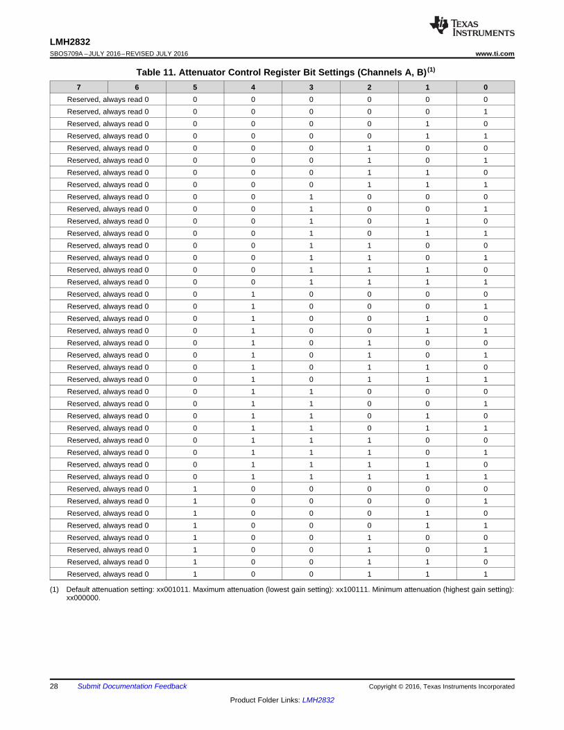
(1) Default value: 001xxxxx. Highest power: 1xxxxxxx. Lower power: 00000000.
Table 10. Bias Control Register Bit Settings (Channels A, B) (1)
7 6 5 4 3 2 1 00 0 0 0 0 0 0 00 0 0 0 0 0 0 10 0 0 0 0 0 1 X0 0 0 0 0 1 X X0 0 0 0 1 X X X0 0 0 1 X X X X0 0 1 X X X X X0 1 X X X X X X1 X X X X X X X
28
LMH2832SBOS709A –JULY 2016–REVISED JULY 2016 www.ti.com
Product Folder Links: LMH2832
Submit Documentation Feedback Copyright © 2016, Texas Instruments Incorporated
(1) Default attenuation setting: xx001011. Maximum attenuation (lowest gain setting): xx100111. Minimum attenuation (highest gain setting):xx000000.
Table 11. Attenuator Control Register Bit Settings (Channels A, B) (1)
7 6 5 4 3 2 1 0Reserved, always read 0 0 0 0 0 0 0Reserved, always read 0 0 0 0 0 0 1Reserved, always read 0 0 0 0 0 1 0Reserved, always read 0 0 0 0 0 1 1Reserved, always read 0 0 0 0 1 0 0Reserved, always read 0 0 0 0 1 0 1Reserved, always read 0 0 0 0 1 1 0Reserved, always read 0 0 0 0 1 1 1Reserved, always read 0 0 0 1 0 0 0Reserved, always read 0 0 0 1 0 0 1Reserved, always read 0 0 0 1 0 1 0Reserved, always read 0 0 0 1 0 1 1Reserved, always read 0 0 0 1 1 0 0Reserved, always read 0 0 0 1 1 0 1Reserved, always read 0 0 0 1 1 1 0Reserved, always read 0 0 0 1 1 1 1Reserved, always read 0 0 1 0 0 0 0Reserved, always read 0 0 1 0 0 0 1Reserved, always read 0 0 1 0 0 1 0Reserved, always read 0 0 1 0 0 1 1Reserved, always read 0 0 1 0 1 0 0Reserved, always read 0 0 1 0 1 0 1Reserved, always read 0 0 1 0 1 1 0Reserved, always read 0 0 1 0 1 1 1Reserved, always read 0 0 1 1 0 0 0Reserved, always read 0 0 1 1 0 0 1Reserved, always read 0 0 1 1 0 1 0Reserved, always read 0 0 1 1 0 1 1Reserved, always read 0 0 1 1 1 0 0Reserved, always read 0 0 1 1 1 0 1Reserved, always read 0 0 1 1 1 1 0Reserved, always read 0 0 1 1 1 1 1Reserved, always read 0 1 0 0 0 0 0Reserved, always read 0 1 0 0 0 0 1Reserved, always read 0 1 0 0 0 1 0Reserved, always read 0 1 0 0 0 1 1Reserved, always read 0 1 0 0 1 0 0Reserved, always read 0 1 0 0 1 0 1Reserved, always read 0 1 0 0 1 1 0Reserved, always read 0 1 0 0 1 1 1
10
10
½ LMH2832
INPx
INMx
OUTPx
OUTMx
RO
RO
SPI
VS+ = 5V
GND
1:3
OUT_AMP+-
ADC
ZS = 50-
Copyright © 2016, Texas Instruments Incorporated
LPF
29
LMH2832www.ti.com SBOS709A –JULY 2016–REVISED JULY 2016
Product Folder Links: LMH2832
Submit Documentation FeedbackCopyright © 2016, Texas Instruments Incorporated
10 Application and Implementation
NOTEInformation in the following applications sections is not part of the TI componentspecification, and TI does not warrant its accuracy or completeness. TI’s customers areresponsible for determining suitability of components for their purposes. Customers shouldvalidate and test their design implementation to confirm system functionality.
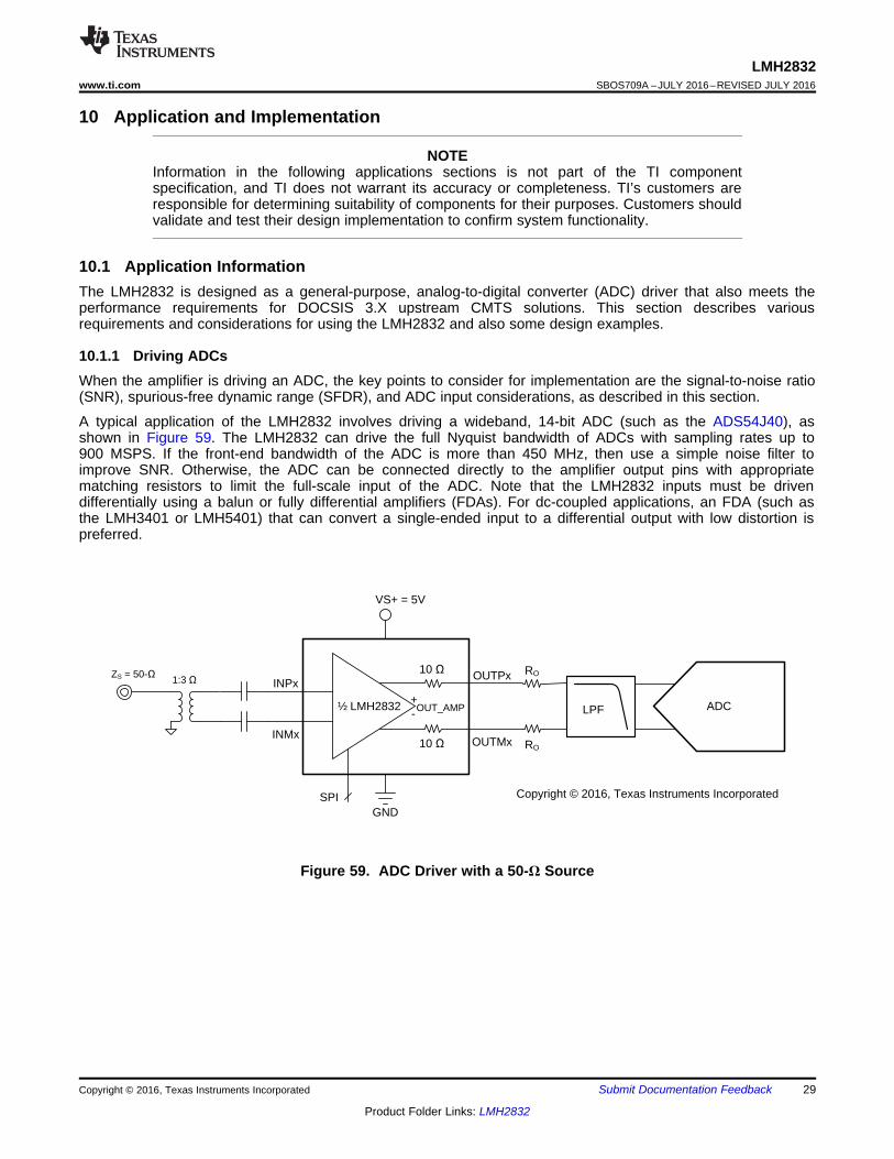
10.1 Application InformationThe LMH2832 is designed as a general-purpose, analog-to-digital converter (ADC) driver that also meets theperformance requirements for DOCSIS 3.X upstream CMTS solutions. This section describes variousrequirements and considerations for using the LMH2832 and also some design examples.
10.1.1 Driving ADCsWhen the amplifier is driving an ADC, the key points to consider for implementation are the signal-to-noise ratio(SNR), spurious-free dynamic range (SFDR), and ADC input considerations, as described in this section.
A typical application of the LMH2832 involves driving a wideband, 14-bit ADC (such as the ADS54J40), asshown in Figure 59. The LMH2832 can drive the full Nyquist bandwidth of ADCs with sampling rates up to900 MSPS. If the front-end bandwidth of the ADC is more than 450 MHz, then use a simple noise filter toimprove SNR. Otherwise, the ADC can be connected directly to the amplifier output pins with appropriatematching resistors to limit the full-scale input of the ADC. Note that the LMH2832 inputs must be drivendifferentially using a balun or fully differential amplifiers (FDAs). For dc-coupled applications, an FDA (such asthe LMH3401 or LMH5401) that can convert a single-ended input to a differential output with low distortion ispreferred.
Figure 59. ADC Driver with a 50-Ω Source
HD =x -SYSTEM 20 log× 10 + 10-HDxAMP+FILTER
20
- ADCHDx
20
SNR = -SYSTEM 20 log× 10 + 10-SNRAMP+FILTER
10
-SNRADC
10
SNR =AMP+FILTER 10 log×
V2O
e2FILTEROUT
= 20 log×
VO
eFILTEROUT
30
LMH2832SBOS709A –JULY 2016–REVISED JULY 2016 www.ti.com
Product Folder Links: LMH2832
Submit Documentation Feedback Copyright © 2016, Texas Instruments Incorporated
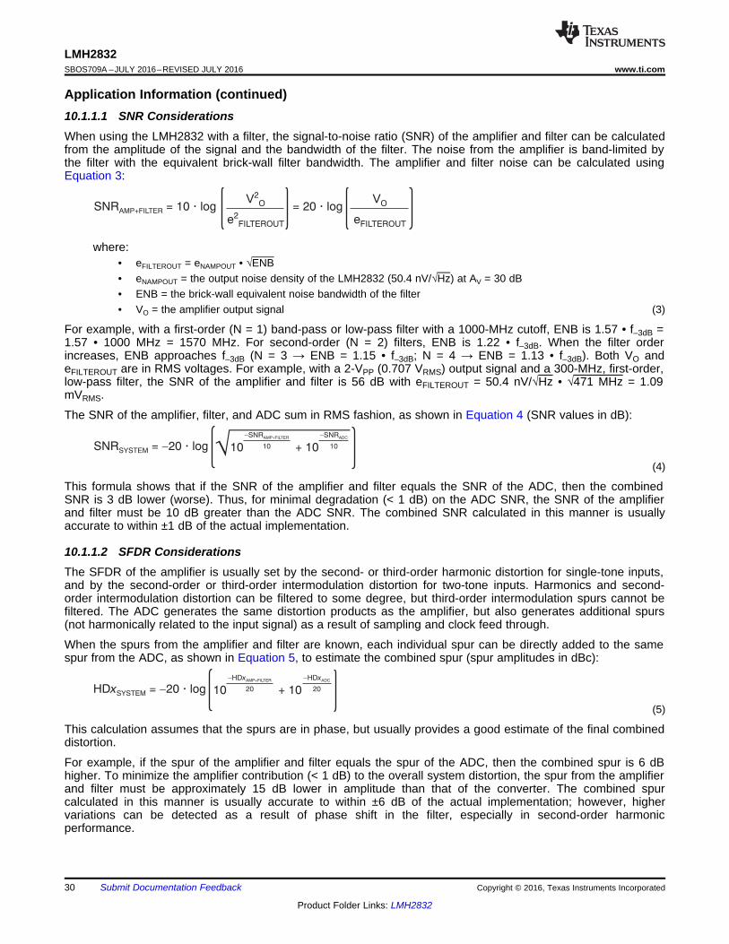
Application Information (continued)10.1.1.1 SNR ConsiderationsWhen using the LMH2832 with a filter, the signal-to-noise ratio (SNR) of the amplifier and filter can be calculatedfrom the amplitude of the signal and the bandwidth of the filter. The noise from the amplifier is band-limited bythe filter with the equivalent brick-wall filter bandwidth. The amplifier and filter noise can be calculated usingEquation 3:
where:• eFILTEROUT = eNAMPOUT • √ENB• eNAMPOUT = the output noise density of the LMH2832 (50.4 nV/√Hz) at AV = 30 dB• ENB = the brick-wall equivalent noise bandwidth of the filter• VO = the amplifier output signal (3)
For example, with a first-order (N = 1) band-pass or low-pass filter with a 1000-MHz cutoff, ENB is 1.57 • f–3dB =1.57 • 1000 MHz = 1570 MHz. For second-order (N = 2) filters, ENB is 1.22 • f–3dB. When the filter orderincreases, ENB approaches f–3dB (N = 3 → ENB = 1.15 • f–3dB; N = 4 → ENB = 1.13 • f–3dB). Both VO andeFILTEROUT are in RMS voltages. For example, with a 2-VPP (0.707 VRMS) output signal and a 300-MHz, first-order,low-pass filter, the SNR of the amplifier and filter is 56 dB with eFILTEROUT = 50.4 nV/√Hz • √471 MHz = 1.09mVRMS.
The SNR of the amplifier, filter, and ADC sum in RMS fashion, as shown in Equation 4 (SNR values in dB):
(4)
This formula shows that if the SNR of the amplifier and filter equals the SNR of the ADC, then the combinedSNR is 3 dB lower (worse). Thus, for minimal degradation (< 1 dB) on the ADC SNR, the SNR of the amplifierand filter must be 10 dB greater than the ADC SNR. The combined SNR calculated in this manner is usuallyaccurate to within ±1 dB of the actual implementation.
10.1.1.2 SFDR ConsiderationsThe SFDR of the amplifier is usually set by the second- or third-order harmonic distortion for single-tone inputs,and by the second-order or third-order intermodulation distortion for two-tone inputs. Harmonics and second-order intermodulation distortion can be filtered to some degree, but third-order intermodulation spurs cannot befiltered. The ADC generates the same distortion products as the amplifier, but also generates additional spurs(not harmonically related to the input signal) as a result of sampling and clock feed through.
When the spurs from the amplifier and filter are known, each individual spur can be directly added to the samespur from the ADC, as shown in Equation 5, to estimate the combined spur (spur amplitudes in dBc):
(5)
This calculation assumes that the spurs are in phase, but usually provides a good estimate of the final combineddistortion.
For example, if the spur of the amplifier and filter equals the spur of the ADC, then the combined spur is 6 dBhigher. To minimize the amplifier contribution (< 1 dB) to the overall system distortion, the spur from the amplifierand filter must be approximately 15 dB lower in amplitude than that of the converter. The combined spurcalculated in this manner is usually accurate to within ±6 dB of the actual implementation; however, highervariations can be detected as a result of phase shift in the filter, especially in second-order harmonicperformance.

Amp
RO
RO
ADC
AIN-
AIN+
CMRCM
RCM
31
LMH2832www.ti.com SBOS709A –JULY 2016–REVISED JULY 2016
Product Folder Links: LMH2832
Submit Documentation FeedbackCopyright © 2016, Texas Instruments Incorporated
Application Information (continued)This worst-case spur calculation assumes that the amplifier and filter spur of interest is in phase with thecorresponding spur in the ADC, such that the two spur amplitudes can be added linearly. There are two phase-shift mechanisms that cause the measured distortion performance of the amplifier-ADC chain to deviate from theexpected performance calculated using Equation 5; one mechanism is the common-mode phase shift and theother is the differential phase shift.
Common-mode phase shift is the phase shift detected equally in both branches of the differential signal pathincluding the filter. Common-mode phase shift nullifies the basic assumption that the amplifier, filter, and ADCspur sources are in phase. This phase shift can lead to better performance than predicted when the spursbecome phase shifted, and there is the potential for cancellation when the phase shift reaches 180°. However,there is a significant challenge in designing an amplifier-ADC interface circuit to take advantage of a common-mode phase shift for cancellation: the phase characteristics of the ADC spur sources are unknown, thus thenecessary phase shift in the filter and signal path for cancellation is also unknown.
Differential phase shift is the difference in the phase response between the two branches of the differential filtersignal path. Differential phase shift in the filter is a result of mismatched components caused by nominaltolerances and can severely degrade the even harmonic distortion of the amplifier-ADC chain. This effect has thesame result as mismatched path lengths for the two differential traces, and causes more phase shift in one paththan the other. Ideally, the phase responses over frequency through the two sides of a differential signal path areidentical, such that even harmonics remain optimally out of phase and cancel when the signal is takendifferentially. However, if one side has more phase shift than the other, then the even harmonic cancellation isnot as effective.
Single-order, resistor-capacitor (RC) filters cause very little differential phase shift with nominal tolerances of 5%or less, but higher-order, inductor-capacitor (LC) filters are very sensitive to component mismatch. For instance,a third-order Butterworth band-pass filter with a 100-MHz center frequency and a 20-MHz bandwidth displays asmuch as 20° of differential phase imbalance in a SPICE Monte Carlo analysis with 2% component tolerances.Therefore, although a prototype may work, production variance is unacceptable. For ac-coupled or dc-coupledapplications where a transformer or balun cannot be used, using first- or second-order filters is recommended tominimize the effect of differential phase shift.
10.1.1.3 ADC Input Common-Mode Voltage Considerations (AC-Coupled Input)When interfacing to an ADC, the input common-mode voltage range of the ADC must be taken into account forproper operation. In an ac-coupled application between the amplifier and the ADC, the input common-modevoltage bias of the ADC can be accomplished in different ways. Some ADCs use internal bias networks such thatthe analog inputs are automatically biased to the required input common-mode voltage if the inputs are ac-coupled with capacitors (or if the filter between the amplifier and ADC is a band-pass filter). Other ADCs supplythe required input common-mode voltage from a reference voltage output pin (often termed CM or VCM). Withthese ADCs, the ac-coupled input signal can be re-biased to the input common-mode voltage by connectingresistors from each input to the CM output of the ADC, as shown in Figure 60. AC coupling provides dc common-mode isolation between the amplifier and the ADC; thus, the output common-mode voltage of the amplifier is adon’t care for the ADC.
Figure 60. Biasing AC-Coupled ADC Inputs Using the ADC CM Output

10
10
½ LMH2832
INPx
INMx
OUTPx
OUTMx
64.9
64.9
SPI
VS+ = 5V
GND
0.1 µF
0.1 µF
0.1 µF
0.1 µF
1:2 O
OUT_AMP+-
½ ADS54J405.5 pF 5.5 pF
24 nH
24 nH
82 nH
82 nH
24 nH
24 nH
100
100
VOCM
5.1
5.1
ZS = 75-
Copyright © 2016, Texas Instruments Incorporated
32
LMH2832SBOS709A –JULY 2016–REVISED JULY 2016 www.ti.com
Product Folder Links: LMH2832
Submit Documentation Feedback Copyright © 2016, Texas Instruments Incorporated
Application Information (continued)10.1.1.4 ADC Input Common-Mode Voltage Considerations (DC-Coupled Input)The LMH2832 is designed to primarily be used in ac-coupled applications only. However, the LMH2832 can bedc-coupled if certain strict conditions are met. The LMH2832 has an internal common-mode bias equal to themid-supply voltage, so any dc coupling on the input or output must have a common-mode voltage that is also setto mid-supply. To dc couple to an ADC input, the mid-supply voltage of the LMH2832 must be centered aroundthe ADC input common-mode. This common-mode matching can be accomplished by shifting the supplies tocenter the mid-supply voltage around the ADC input common-mode voltage. However, shifting the supplies alsochanges the ground reference for the digital inputs, which then likely requires a voltage-shifted interface as well.The LMH2832 is not recommended to be operated as dc-coupled unless absolutely necessary.
10.2 Typical Applications
10.2.1 DOCSIS 3.X DriverThe LMH2832 is designed to perform best when driving differential input ADCs in high-speed applications.Figure 61 shows an example diagram of the LMH2832 driving an ADC with a fifth-order, low-pass filter for a 75-Ωimpedance, data over cable service interface specification (DOCSIS) 3.X upstream receiver return pathapplication. The primary interface between the amplifier and the ADC is usually an antialiasing filter to suppresshigh-frequency harmonics that otherwise alias back into the ADC FFT spectrum. Filters range from single-orderreal RC poles to higher-order, resistor-inductor-capacitor (RLC) filters, depending on the applicationrequirements. Series output resistors (RO) help isolate the amplifier from any capacitive load presented by thefilter, and can also be used to create a matched impedance to drive transmission lines.
Figure 61. DOCSIS 3.X Driver with the ADS54J40 and a 300-MHz, 4th-Order, Butterworth, Low-Pass Filter
10.2.1.1 Design RequirementsTable 12 shows example design requirements for the LMH2832 in an upstream receiver application.
Table 12. Example Design RequirementsSPECIFICATION DESIGN REQUIREMENTS
Supply voltage 4.75 to 5.25 VUsable input frequency range 300 MHz
System voltage gain and range 33-dB voltage gain with 30-dB rangeSource impedance 75 Ω, single-ended
Signal path SNR at 175 MHz (measured at ADC) > 50 dBFS

33
LMH2832www.ti.com SBOS709A –JULY 2016–REVISED JULY 2016
Product Folder Links: LMH2832
Submit Documentation FeedbackCopyright © 2016, Texas Instruments Incorporated
10.2.1.2 Detailed Design ProcedureTo begin the design process, make sure that none of the following design parameters exceed the limits listed inthe Electrical Characteristics table, such as:
• Supply voltage• Temperature range• Input voltage range across gain• Output current requirements• Digital I/O voltages and currents
10.2.1.2.1 Source Resistance Matching
Standard DOCSIS systems use a characteristic single-ended impedance of 75 Ω that must be properly matchedto the 150-Ω differential impedance of the LMH2832. The circuit in Figure 61 uses a transformer with a 1:2-Ωratio to convert the signal from single-ended to differential, and also to match the differential impedance. Thetransformer also adds a signal gain of approximately 3 dB to the system with some insertion loss depending onthe chosen transformer.
10.2.1.2.2 Output Impedance Matching
For the circuit in Figure 61, the output impedance is matched to a 150-Ω characteristic impedance filter tomaximize the performance of the LMH2832. On the amplifier output side, the output impedance is matched to150 Ω by including a 65-Ω series resistor on each output. Combined with the internal 10-Ω resistors on eachoutput, the total differential impedance becomes 150 Ω. The ADS54J40 has an input impedance ofapproximately 600 Ω that is reduced to 150 Ω by using two 5-Ω series input resistors in parallel with two 100-Ωseries resistors. The 5-Ω series resistors are included to isolate the input capacitance of the ADC so that theresponse of the filter is not affected. With both the amplifier and ADC impedances matched, any transmissionline effects of the connection are minimized.
If the ADC is physically located close enough to the amplifier, a matched impedance may not be needed; seeDriving Low Insertion-Loss Filters section for more information on driving non-matched filters.
10.2.1.2.3 Voltage Headroom Considerations
Because of the series resistors included on both the amplifier outputs and ADC inputs, the amplifier must drive avoltage that is significantly higher than the ADC full-scale input. For the circuit in Figure 61, the ADS54J40 full-scale input voltage is 1.9 VPP, so the required voltage at the amplifier output pins is 3.6 VPP. This voltage is lessthan the specified output voltage of 5 VPP for the LMH2832, thus system performance is not limited. If therequired output voltage is higher than what the amplifier can support, then the matched resistance value can bereduced. However, this reduction can have performance implications because more current output is requiredfrom the amplifier.
The input voltage swing can be larger than the output voltage swing because the LMH2832 can operate as anattenuator. To maintain the full-scale voltage of the ADS54J40 input in this application, the amplifier cannotattenuate more than 1 dB from input to output; otherwise, the maximum input voltage swing is exceeded. If theamplifier must be operated with more attenuation, then the output voltage must be reduced.

LMH2832 ADS54J60
RF IN
I Channel
Q Channel
LPF
LPF
Copyright © 2016, Texas Instruments Incorporated
Frequency (MHz)
Cha
nnel
-to-
Cha
nnel
Isol
atio
n (d
Bc)
0 50 100 150 200 250 300 350 400 450 500-110
-100
-90
-80
-70
-60
-50
-40
D037
Channel A to BChannel B to A
34
LMH2832SBOS709A –JULY 2016–REVISED JULY 2016 www.ti.com
Product Folder Links: LMH2832
Submit Documentation Feedback Copyright © 2016, Texas Instruments Incorporated
10.2.1.3 Application Curve
Figure 62. Amplifier Dual Channel Isolation Presented to ADC Interface
10.2.2 IQ ReceiverThe LMH2832 is a dual-channel device; therefore, the device has excellent gain and phase matching betweenchannels A and B. This matching makes the LMH2832 an excellent choice for systems that require two matchedchannels (such as an IQ demodulation receiver), as shown in Figure 63. For an IQ system, both the gain andphase must match for the real and imaginary channel. When using two single-channel amplifiers, the matchingcharacteristics are subject to process lot and packaging variations for two individual devices, and there is oftenno way to make sure that the amplifiers match without testing each amplifier. However, the dual-channelarchitecture of the LMH2832 allows for much tighter gain and phase matching with minimal crosstalk effects. Formore matching information, see the Electrical Characteristics table.
Figure 63. IQ Receiver Block Diagram
35
LMH2832www.ti.com SBOS709A –JULY 2016–REVISED JULY 2016
Product Folder Links: LMH2832
Submit Documentation FeedbackCopyright © 2016, Texas Instruments Incorporated
10.3 Do's and Don'ts
10.3.1 Do:• Include a thermal analysis at the beginning of the project• Use well-terminated transmission lines for all signals• Maintain symmetrical input and output trace layouts• Use solid metal layers for the power supplies• Keep signal lines as straight as possible
10.3.2 Don't:• Use a lower power-supply voltage than necessary• Forget about the common-mode response of filters and transmission lines• Rout digital line traces close to the analog signals and supply line traces
11 Power Supply RecommendationsThe LMH2832 is designed to be used with a single supply with a range of 4.75 V to 5.25 V. The ideal supplyvoltage is a 5.0-V total single-ended supply. If the supply is reduced to the minimum voltage, then the maximuminput and output voltage range is reduced by 0.25 V.
11.1 Split SuppliesIdeally, the LMH2832 uses a single-ended, 5-V supply, but the device can be operated on a split supply ifnecessary. However, the digital logic is referenced to the GND pins, meaning that the logic reference shifts withthe GND supply if connected to a negative voltage and must be accounted for in the logic connections. Ingeneral, the LMH2832 is not suggested to be operated with a split-supply configuration.
11.2 Supply DecouplingPower-supply decoupling is critical to high-frequency performance. Onboard bypass capacitors are used on theLMH2832EVM; however, the most important component of the supply bypassing is provided by the printed circuitboard (PCB). As illustrated in Figure 64, there are multiple vias connecting the LMH2832 power planes to thepower-supply traces. These vias connect the internal power planes to the LMH2832. Both VCC and GND must beconnected to the internal power planes with several square centimeters of continuous plane in the immediatevicinity of the amplifier. The capacitance between these power planes provides the bulk of the high-frequencybypassing for the LMH2832.

36
LMH2832SBOS709A –JULY 2016–REVISED JULY 2016 www.ti.com
Product Folder Links: LMH2832
Submit Documentation Feedback Copyright © 2016, Texas Instruments Incorporated
12 Layout
12.1 Layout GuidelinesWith a small bandwidth greater than 1 GHz, layout for the LMH2832 is critical and nothing can be neglected. Inorder to simplify board design, the LMH2832 has on-chip resistors that reduce the affect of off-chip capacitance.For this reason, make sure that the ground layer below the LMH2832 is not cut. The recommendation to not cutthe ground plane under the amplifier input and output pins is different than many other high-speed amplifiers, butthe reason is that parasitic inductance is more harmful to the LMH2832 performance than parasitic capacitance.By leaving the ground layer under the device intact, parasitic inductance of the output and power traces isminimized. The DUT portion of the evaluation board layout is shown in Figure 64.
The EVM uses long-edge capacitors for the decoupling capacitors, which reduces series resistance andincreases the resonant frequency. Vias are also placed to the power planes before the bypass capacitors.Although not evident in the top layer, two vias are used at the capacitor in addition to the two vias underneath thedevice.
The output-matching resistors are 0402 size and are placed very close to the amplifier output pins, whichreduces both parasitic inductance and capacitance. The use of 0603 output-matching resistors produces ameasurable decrease in bandwidth.
When the signal is on a 50-Ω or 75-Ω controlled impedance transmission line, the layout then becomes muchless critical. The transition from the 50-Ω or 75-Ω transmission line to the amplifier pins is the most critical area.
12.2 Layout Example
Figure 64. Layout Example

LMH2832
IRHA
TI YMS
LLLL
Legend:
= Pin 1 Designator
LMH2832 = Device Name
TI = Texas Instruments
YM = Year Month Date Code
S = Assembly Site Code
LLLL = Assembly Lot Code
37
LMH2832www.ti.com SBOS709A –JULY 2016–REVISED JULY 2016
Product Folder Links: LMH2832
Submit Documentation FeedbackCopyright © 2016, Texas Instruments Incorporated
13 Device and Documentation Support
13.1 Device Support
13.1.1 Device Nomenclature
Figure 65. Device Marking Information
13.2 Documentation Support
13.2.1 Related DocumentationFor related documentation see the following:• ADS54J40 Dual-Channel, 14-Bit, 1.0-GSPS Analog-to-Digital Converter Data Sheet (SBAS714)• LMH3401 7-GHz, Ultra-Wideband, Fixed-Gain, Fully-Differential Amplifier Data Sheet (SBOS695)• LMH5401 8-GHz, Low-Noise, Low-Power, Fully-Differential Amplifier Data Sheet (SBOS710)• LMH6521 High Performance Dual DVGA Data Sheet (SNOSB47)• LMH3404 Dual-Channel, 7-GHz, Low-Noise, Low-Power, Fully Differential Amplifier Data Sheet (SBOS739)• LMH3402 Dual, Selectable-Gain, 7-GHz, Low-Noise, Low-Power, Fully Differential Amplifier Data Sheet
(SBOS744)• LMH2832EVM-50 Evaluation Module User's Guide (SLOU454)• LMH2832EVM-75 Evaluation Module User's Guide (SLOU438)• LMH2832 TINA-TI Reference Design (SBOMA21)• LMH2832 TINA-TI Spice Model (SBOMA22)
13.3 Receiving Notification of Documentation UpdatesTo receive notification of documentation updates, navigate to the device product folder on ti.com. In the upperright corner, click on Alert me to register and receive a weekly digest of any product information that haschanged. For change details, review the revision history included in any revised document.
13.4 Community ResourcesThe following links connect to TI community resources. Linked contents are provided "AS IS" by the respectivecontributors. They do not constitute TI specifications and do not necessarily reflect TI's views; see TI's Terms ofUse.
TI E2E™ Online Community TI's Engineer-to-Engineer (E2E) Community. Created to foster collaborationamong engineers. At e2e.ti.com, you can ask questions, share knowledge, explore ideas and helpsolve problems with fellow engineers.
Design Support TI's Design Support Quickly find helpful E2E forums along with design support tools andcontact information for technical support.
13.5 TrademarksE2E is a trademark of Texas Instruments.Keysight Technologies is a trademark of Keysight Technologies.SPI is a trademark of Motorola Mobility LLC.All other trademarks are the property of their respective owners.

38
LMH2832SBOS709A –JULY 2016–REVISED JULY 2016 www.ti.com
Product Folder Links: LMH2832
Submit Documentation Feedback Copyright © 2016, Texas Instruments Incorporated
13.6 Electrostatic Discharge CautionThis integrated circuit can be damaged by ESD. Texas Instruments recommends that all integrated circuits be handled withappropriate precautions. Failure to observe proper handling and installation procedures can cause damage.
ESD damage can range from subtle performance degradation to complete device failure. Precision integrated circuits may be moresusceptible to damage because very small parametric changes could cause the device not to meet its published specifications.
13.7 GlossarySLYZ022 — TI Glossary.
This glossary lists and explains terms, acronyms, and definitions.
14 Mechanical, Packaging, and Orderable InformationThe following pages include mechanical, packaging, and orderable information. This information is the mostcurrent data available for the designated devices. This data is subject to change without notice and revision ofthis document. For browser-based versions of this data sheet, refer to the left-hand navigation.

PACKAGE OPTION ADDENDUM
www.ti.com 22-Jul-2016
Addendum-Page 1
PACKAGING INFORMATION
Orderable Device Status(1)
Package Type PackageDrawing
Pins PackageQty
Eco Plan(2)
Lead/Ball Finish(6)
MSL Peak Temp(3)
Op Temp (°C) Device Marking(4/5)
Samples
LMH2832IRHAR ACTIVE VQFN RHA 40 2500 Green (RoHS& no Sb/Br)
CU NIPDAU Level-3-260C-168 HR -40 to 85 LMH2832IRHA
LMH2832IRHAT ACTIVE VQFN RHA 40 250 Green (RoHS& no Sb/Br)
CU NIPDAU Level-3-260C-168 HR -40 to 85 LMH2832IRHA
(1) The marketing status values are defined as follows:ACTIVE: Product device recommended for new designs.LIFEBUY: TI has announced that the device will be discontinued, and a lifetime-buy period is in effect.NRND: Not recommended for new designs. Device is in production to support existing customers, but TI does not recommend using this part in a new design.PREVIEW: Device has been announced but is not in production. Samples may or may not be available.OBSOLETE: TI has discontinued the production of the device.
(2) Eco Plan - The planned eco-friendly classification: Pb-Free (RoHS), Pb-Free (RoHS Exempt), or Green (RoHS & no Sb/Br) - please check http://www.ti.com/productcontent for the latest availabilityinformation and additional product content details.TBD: The Pb-Free/Green conversion plan has not been defined.Pb-Free (RoHS): TI's terms "Lead-Free" or "Pb-Free" mean semiconductor products that are compatible with the current RoHS requirements for all 6 substances, including the requirement thatlead not exceed 0.1% by weight in homogeneous materials. Where designed to be soldered at high temperatures, TI Pb-Free products are suitable for use in specified lead-free processes.Pb-Free (RoHS Exempt): This component has a RoHS exemption for either 1) lead-based flip-chip solder bumps used between the die and package, or 2) lead-based die adhesive used betweenthe die and leadframe. The component is otherwise considered Pb-Free (RoHS compatible) as defined above.Green (RoHS & no Sb/Br): TI defines "Green" to mean Pb-Free (RoHS compatible), and free of Bromine (Br) and Antimony (Sb) based flame retardants (Br or Sb do not exceed 0.1% by weightin homogeneous material)
(3) MSL, Peak Temp. - The Moisture Sensitivity Level rating according to the JEDEC industry standard classifications, and peak solder temperature.
(4) There may be additional marking, which relates to the logo, the lot trace code information, or the environmental category on the device.
(5) Multiple Device Markings will be inside parentheses. Only one Device Marking contained in parentheses and separated by a "~" will appear on a device. If a line is indented then it is a continuationof the previous line and the two combined represent the entire Device Marking for that device.
(6) Lead/Ball Finish - Orderable Devices may have multiple material finish options. Finish options are separated by a vertical ruled line. Lead/Ball Finish values may wrap to two lines if the finishvalue exceeds the maximum column width.
Important Information and Disclaimer:The information provided on this page represents TI's knowledge and belief as of the date that it is provided. TI bases its knowledge and belief on informationprovided by third parties, and makes no representation or warranty as to the accuracy of such information. Efforts are underway to better integrate information from third parties. TI has taken andcontinues to take reasonable steps to provide representative and accurate information but may not have conducted destructive testing or chemical analysis on incoming materials and chemicals.TI and TI suppliers consider certain information to be proprietary, and thus CAS numbers and other limited information may not be available for release.
PACKAGE OPTION ADDENDUM
www.ti.com 22-Jul-2016
Addendum-Page 2
In no event shall TI's liability arising out of such information exceed the total purchase price of the TI part(s) at issue in this document sold by TI to Customer on an annual basis.

TAPE AND REEL INFORMATION
*All dimensions are nominal
Device PackageType
PackageDrawing
Pins SPQ ReelDiameter
(mm)
ReelWidth
W1 (mm)
A0(mm)
B0(mm)
K0(mm)
P1(mm)
W(mm)
Pin1Quadrant
LMH2832IRHAR VQFN RHA 40 2500 330.0 16.4 6.3 6.3 1.1 12.0 16.0 Q2
LMH2832IRHAT VQFN RHA 40 250 180.0 16.4 6.3 6.3 1.1 12.0 16.0 Q2
PACKAGE MATERIALS INFORMATION
www.ti.com 22-Jul-2016
Pack Materials-Page 1

*All dimensions are nominal
Device Package Type Package Drawing Pins SPQ Length (mm) Width (mm) Height (mm)
LMH2832IRHAR VQFN RHA 40 2500 367.0 367.0 38.0
LMH2832IRHAT VQFN RHA 40 250 210.0 185.0 35.0
PACKAGE MATERIALS INFORMATION
www.ti.com 22-Jul-2016
Pack Materials-Page 2
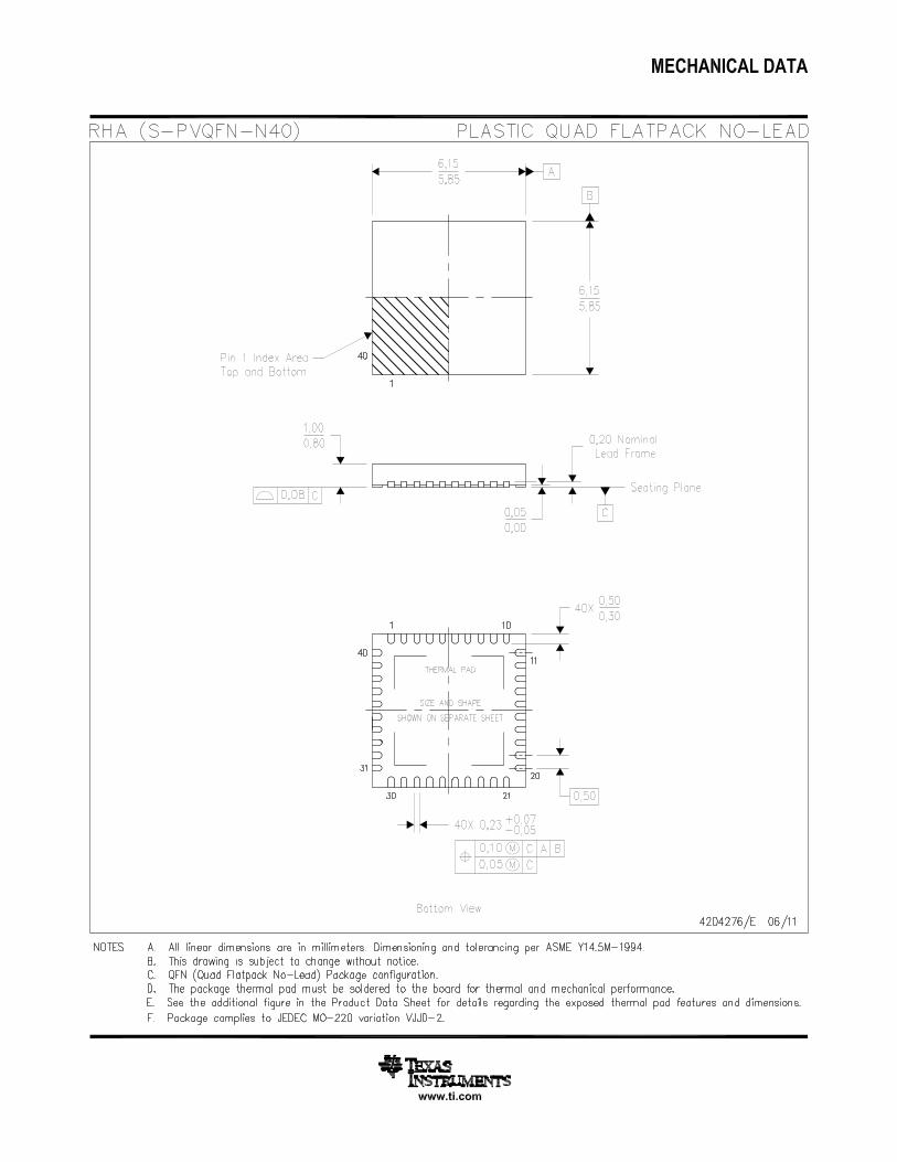


IMPORTANT NOTICE
Texas Instruments Incorporated and its subsidiaries (TI) reserve the right to make corrections, enhancements, improvements and otherchanges to its semiconductor products and services per JESD46, latest issue, and to discontinue any product or service per JESD48, latestissue. Buyers should obtain the latest relevant information before placing orders and should verify that such information is current andcomplete. All semiconductor products (also referred to herein as “components”) are sold subject to TI’s terms and conditions of salesupplied at the time of order acknowledgment.TI warrants performance of its components to the specifications applicable at the time of sale, in accordance with the warranty in TI’s termsand conditions of sale of semiconductor products. Testing and other quality control techniques are used to the extent TI deems necessaryto support this warranty. Except where mandated by applicable law, testing of all parameters of each component is not necessarilyperformed.TI assumes no liability for applications assistance or the design of Buyers’ products. Buyers are responsible for their products andapplications using TI components. To minimize the risks associated with Buyers’ products and applications, Buyers should provideadequate design and operating safeguards.TI does not warrant or represent that any license, either express or implied, is granted under any patent right, copyright, mask work right, orother intellectual property right relating to any combination, machine, or process in which TI components or services are used. Informationpublished by TI regarding third-party products or services does not constitute a license to use such products or services or a warranty orendorsement thereof. Use of such information may require a license from a third party under the patents or other intellectual property of thethird party, or a license from TI under the patents or other intellectual property of TI.Reproduction of significant portions of TI information in TI data books or data sheets is permissible only if reproduction is without alterationand is accompanied by all associated warranties, conditions, limitations, and notices. TI is not responsible or liable for such altereddocumentation. Information of third parties may be subject to additional restrictions.Resale of TI components or services with statements different from or beyond the parameters stated by TI for that component or servicevoids all express and any implied warranties for the associated TI component or service and is an unfair and deceptive business practice.TI is not responsible or liable for any such statements.Buyer acknowledges and agrees that it is solely responsible for compliance with all legal, regulatory and safety-related requirementsconcerning its products, and any use of TI components in its applications, notwithstanding any applications-related information or supportthat may be provided by TI. Buyer represents and agrees that it has all the necessary expertise to create and implement safeguards whichanticipate dangerous consequences of failures, monitor failures and their consequences, lessen the likelihood of failures that might causeharm and take appropriate remedial actions. Buyer will fully indemnify TI and its representatives against any damages arising out of the useof any TI components in safety-critical applications.In some cases, TI components may be promoted specifically to facilitate safety-related applications. With such components, TI’s goal is tohelp enable customers to design and create their own end-product solutions that meet applicable functional safety standards andrequirements. Nonetheless, such components are subject to these terms.No TI components are authorized for use in FDA Class III (or similar life-critical medical equipment) unless authorized officers of the partieshave executed a special agreement specifically governing such use.Only those TI components which TI has specifically designated as military grade or “enhanced plastic” are designed and intended for use inmilitary/aerospace applications or environments. Buyer acknowledges and agrees that any military or aerospace use of TI componentswhich have not been so designated is solely at the Buyer's risk, and that Buyer is solely responsible for compliance with all legal andregulatory requirements in connection with such use.TI has specifically designated certain components as meeting ISO/TS16949 requirements, mainly for automotive use. In any case of use ofnon-designated products, TI will not be responsible for any failure to meet ISO/TS16949.
Products ApplicationsAudio www.ti.com/audio Automotive and Transportation www.ti.com/automotiveAmplifiers amplifier.ti.com Communications and Telecom www.ti.com/communicationsData Converters dataconverter.ti.com Computers and Peripherals www.ti.com/computersDLP® Products www.dlp.com Consumer Electronics www.ti.com/consumer-appsDSP dsp.ti.com Energy and Lighting www.ti.com/energyClocks and Timers www.ti.com/clocks Industrial www.ti.com/industrialInterface interface.ti.com Medical www.ti.com/medicalLogic logic.ti.com Security www.ti.com/securityPower Mgmt power.ti.com Space, Avionics and Defense www.ti.com/space-avionics-defenseMicrocontrollers microcontroller.ti.com Video and Imaging www.ti.com/videoRFID www.ti-rfid.comOMAP Applications Processors www.ti.com/omap TI E2E Community e2e.ti.comWireless Connectivity www.ti.com/wirelessconnectivity
Mailing Address: Texas Instruments, Post Office Box 655303, Dallas, Texas 75265Copyright © 2016, Texas Instruments Incorporated