mars mv converter input plane design and implementation shuai lu, prof el-sharkawi ee, university of...
TRANSCRIPT

MARS MV converter input plane design and implementation
Shuai Lu, Prof El-Sharkawi
EE, University of Washington
March 29, 2005

Outline
• Input plane components overview
• MV switching circuit topology
• Converter startup power supply
• Switching operation and AB selection logic
• MV voltage and current measurement

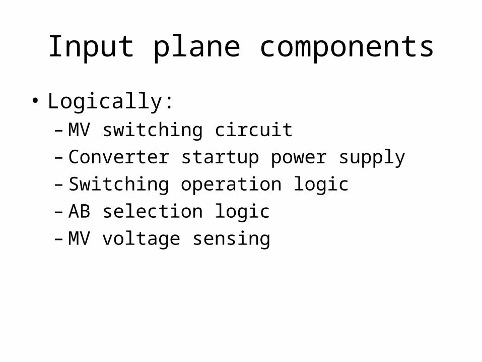
Input plane components
• Physically:– MV switching board, including MV switches,
voltage dividers, (isolation diodes), charging resistors, etc. Mostly HV parts
– MV logic board, including converter startup power supply, switching control logic circuit, and MV voltage sensing circuit. All LV parts.
Input plane components
• Logically:– MV switching circuit– Converter startup power supply– Switching operation logic– AB selection logic– MV voltage sensing

MV switching circuit
ConverterB
ConverterA
V_in_A
V_in_B
S1_AS2
(2)(1) (3) (4) (5)
-10kV in400V out
S1_B3k
Diodes: isolate positive voltage from converter input
S1_A and S1_B: 10kV isolation switches
3k ohm resistor: limits charging current when connecting converters to 10kV
S2: bypass 10kV isolation switch

MV switching circuit
• Rules behind switching operations:– Two converters, one in cold standby (means
when one is working, another is isolated from 10kV)
– When one converter has fault, it should be isolated so that the other one will work.
– Switches not close to a load or open with current flowing at voltage higher than 500V (means S1 and S2 have to be latching switches, and operated at low voltage)

Converter startup power supply
• Functions:– Supply power to logic circuit to operate switches– Supply power to converter gate signal for startup. Requires 20-
25W, 10V for at least 4ms.– Must be available when converter is not running. Therefore after
converter is shutdown for load fault, it can still be started.• The last two points mean that the startup power supply
has to be periodical pulse. Otherwise, it’ll consume too much energy. (25W constantly)
• Startup power supply has to be available both at low voltage for switching operations and high voltage for starting converter.
• A 12V voltage regulator with input from 100V to 10kV, positive or negative.

Converter startup power supply
Waveform at positive voltage (Sing_vin=0), switches are being opened:
1: VCC (inverted) 2: NAND gate output

Converter startup power supply
Waveform at positive voltage (Sing_vin=0), switches are already opened:
1: VCC (inverted) 2: NAND gate output

Converter startup power supply
Waveform at negative voltage (Sing_vin=1), when switches are being closed:
1: counter clock signal
2: fault detection circuit voltage sensing output (ignore the spikes, it can be seen as VCC inverted)

Switching operation logic
• Functions:– Open all switches (S1 and S2) at positive
voltage– Close S1 at negative voltage – Check fault at place (4), i.e., converter input. If
fault exists, open S1.

Switching operation logic
Voltage polarity sensing
Fault voltage detection
VCC low detection
30 Hz Counter
Logic functions
&0
0
0 0
Relay driving circuit
Switching operation logic circuit diagram

Switching operation logic
Open all switchesVflag=1
V_in=-500V
Close S1_A
Fault
No fault
Open S1_A,
A_Ok=1Close S1_B
Fault
No fault
Open S1_B,
t0 t1 t2 t3 t4 t5
Vflag=1
Vflag=0
A_Ok=0 B_Ok=0
B_Ok=1 Vflag=0
V_in=+500V
Logic sequence for switching operations
A_OK and B_OK are indicating the fault status of converter input. They are sent to node controller.

Switching operation logic
Vin = -500V. When S1_A has 250k fault, S1_B has 500k fault.
1: clock signal
2: LPF(CA3140) output in fault detection circuit

Switching operation logic
Vin = -500V. When S1_A has 250k fault, S1_B has no fault.
1: clock signal
2: LPF(CA3140) output in fault detection circuit

Switching operation logic
Vin = -500V. When S1_A no fault, S1_B has no fault.
1: clock signal
2: LPF(CA3140) output in fault detection circuit

Switching operation logic
Vin = -500V. When S1_A has 250k fault, S1_B has 500k fault. Whole process view.
1: clock signal2: LPF(CA3140) output in fault detection circuit

AB selection logic
• Functions:– Close S2 after Vin is higher than threshold
voltage(5.3kV).– Close S3 to give converter gate signal to start
it.– When converter A works, open S1_B to
isolate B from 10kV.– When converter A doesn’t work, open S1_A
and starts B.

AB selection logic
Vlotage sensing hysteresis circuit
400V_OK detection
Status memory(counter with cap)
Logic functions Relay driving circuit
clock
reset
AB selection logic circuit diagram

AB selection logic
When converter is successfully started:
1: S3_A closing signal
2: VCC (inverted)

AB selection logic
When converter is successfully started:
1: S3_A closing signal
2: S2 closing signal (inverted) 15ms earlier than S3_A closing signal

AB selection logic
When converter is not successfully started:
1: S3_A closing signal
2: VCC (inverted) (the drop at the end is caused by the 3.6 ohm resistor simulating converter gate driving circuit)

Voltage measurement result
Vin 6.03 6.53 7.03 7.53 8.04 9.04 9.54 10.04 10.55
Vmeas 6.015 6.515 7.017 7.529 8.037 9.045 9.551 10.046 10.573
1 2 3 4 5 6 7 8 96
6.5
7
7.5
8
8.5
9
9.5
10
10.5
11
Measurement
Cab
le V
olta
ge(k
V)
real valueVmeas