master report - aau
TRANSCRIPT
DESIGN & I MPLEMENTATION OF FPGA-BASED
MULTI -STANDARD SOFTWARE RADIO RECEIVER
E-STUDYBOARD
AALBORG UNIVERSITY
GROUP ASPI-1044MASTERS’ T HESIS, JUNE 2007


Aalborg UniversityE-StudyboardApplied Signal Processing and Implementation 10th Semester
TITLE:
Design & Implementation of FPGA-based Multi-standard Software Radio Receiver
PROJECT PERIOD:P102nd February -7th June 2007
PROJECT GROUP:ASPI10-2007 - Gr. 1044
GROUP MEMBERS:Mehmood-Ur-Rehman AwanMuhammad Mahtab Alam
PROJECT SUPERVISORS:Peter KochNastaran Behjou
Publications: 5
Total number of pages:138
ABSTRACT:
The objective of the project was to design and imple-ment FPGA-based Multi-standard Software Radio Receiver.WLAN and UMTS are taken as case study. Xilinx FPGAVirtex-IV is the target platform. Bandpass sampling tech-nique at 840MHz is used to alias the combined band ofWLAN and UMTS. The WLAN and UMTS channels arerequired at baseband with the sampling rate of 20MHz and61.44MHz respectively. Bandpass filters are used to separatethe UMTS and WLAN bands. In the channelization process,in contrast to conventional channelizer, polyphase channel-izer is used. In the simulations, optimal-method-based FIRfilters are used. In polyphase channelizers, the prototypefilter for WLAN has 50 taps, partitioned into 5 polyphasesub-filters whereas the prototype filter for UMTS has 2520taps, partitioned into 210 polyphase sub-filters. The receivedchannels at baseband has 50dB of dynamic range. In theimplementation, different structures for polyphase channel-izer are considered (such as) standard structure, symmetric-property based structure, Adder shared structure and serialpolyphase structure with serial and parallel MAC. Serialpolyphase structure with parallel MAC is selected. In the in-dividual sub-filter implementation, different implementationstructures are considered. These being Parallel Multipliersand Accumulate, Bit systolic array, Distributed Arithmetic(DA), Fast FIR, Frequency domain filtering and Multiplier-Less filtering techniques. An analysis based on the approxi-mations for the area requirements for multipliers, adders andregisters for these structures is performed. For 16-tap filter,the structures for Parallel-Multiply and accumulate, DA, FastFIR and Frequency domain filtering require 2896 (withoutadders), 3072, 4064, and 5572 slices, respectively. The DAis found to be suitable for the implementation due to beingresource efficient. Polyphase sub-filter is implemented withDistributed Arithmetic structure or with Xilinx-DSP48 slicesfor improved performance.

PREFACE
This report is written by group 1044, studying the master specialization Applied Signal Processingand Implementation (ASPI) at Aalborg University. The report serves as documentation of theThesis work at the 10th semester.
The introduction provides a rationale for the project, and leads to a definition of the problem.The problem is specified in the problem statement, which leads to a definition of the modulesnecessary for the project. The functionality of the algorithms are examined in the Software RadioSystem Design, WLAN and UMTS Channelizers, and Simulationschapters, and the mapping ofthe algorithm to the architecture is conducted in the Algorithm-to-Architecture-Mapping chapter.
The appendices expand on some of the details in the project, where it is not strictly necessaryin the main report.
All chapters, sections, figures, and tables have assigned numbers, and the reference will makeclear, whether the reference is made for figures or tables. The equations are assigned numbers,and the reference for an equation is shown in parentheses. References to the bibliography are doneusing Harvard citation style, e.g. [Haykin, 2002, p. 205]
The enclosed CD-ROM contains all the relevant MatLab scripts, and VHDL codes used in theproject.
Muhammad Mahtab Alam Mehmood-Ur-Rehman Awan
i

TABLE OF CONTENTS
1 Introduction 11.1 Wireless Radio’s . . . . . . . . . . . . . . . . . . . . . . . . . . . . . . . . .. 11.2 Problem Description . . . . . . . . . . . . . . . . . . . . . . . . . . . . . .. . 4
2 Software Radio System Design 112.1 Downconversion Techniques for Software Radio . . . . . . . .. . . . . . . . . . 112.2 Architecture Selection . . . . . . . . . . . . . . . . . . . . . . . . . . .. . . . 142.3 Design Process . . . . . . . . . . . . . . . . . . . . . . . . . . . . . . . . . . .142.4 Channelization . . . . . . . . . . . . . . . . . . . . . . . . . . . . . . . . . .. 162.5 Polyphase Channelization . . . . . . . . . . . . . . . . . . . . . . . . .. . . . . 182.6 Polyphase filter bank parameters . . . . . . . . . . . . . . . . . . . .. . . . . . 252.7 Maximally decimated filter bank . . . . . . . . . . . . . . . . . . . . .. . . . . 252.8 Polyphase Computational Complexity . . . . . . . . . . . . . . . .. . . . . . . 26
3 WLAN and UMTS Channelizers 293.1 WLAN and UMTS Channelizers . . . . . . . . . . . . . . . . . . . . . . . . .. 293.2 Modified System Design . . . . . . . . . . . . . . . . . . . . . . . . . . . . .. 343.3 Sampling Rate Changes . . . . . . . . . . . . . . . . . . . . . . . . . . . . .. . 373.4 Observations . . . . . . . . . . . . . . . . . . . . . . . . . . . . . . . . . . . .44
4 Simulations 514.1 Digital Filter . . . . . . . . . . . . . . . . . . . . . . . . . . . . . . . . . . .. . 524.2 Polyphase Channelizers . . . . . . . . . . . . . . . . . . . . . . . . . . .. . . . 604.3 Conclusion . . . . . . . . . . . . . . . . . . . . . . . . . . . . . . . . . . . . . 66
5 Implementation Analysis 695.1 Polyphase Filter Structure . . . . . . . . . . . . . . . . . . . . . . . .. . . . . . 695.2 Symmetric Structure . . . . . . . . . . . . . . . . . . . . . . . . . . . . . .. . 715.3 Serial Polyphase Filter Bank . . . . . . . . . . . . . . . . . . . . . . .. . . . . 755.4 Conclusion . . . . . . . . . . . . . . . . . . . . . . . . . . . . . . . . . . . . . 765.5 FIR Filtering . . . . . . . . . . . . . . . . . . . . . . . . . . . . . . . . . . . . 775.6 Cost Function for the Implementation . . . . . . . . . . . . . . . .. . . . . . . 995.7 Design Space Exploration . . . . . . . . . . . . . . . . . . . . . . . . . .. . . . 99
iii

TABLE OF CONTENTS
6 Algorithm-to-Architecture Mapping 1016.1 Parallel Multipliers and Accumulators . . . . . . . . . . . . . .. . . . . . . . . 1026.2 Bit Systolic Array Architecture . . . . . . . . . . . . . . . . . . . .. . . . . . . 1036.3 Fast FIR Algorithm . . . . . . . . . . . . . . . . . . . . . . . . . . . . . . . .. 1096.4 Frequency Domain Filtering . . . . . . . . . . . . . . . . . . . . . . . .. . . . 1106.5 Conclusion . . . . . . . . . . . . . . . . . . . . . . . . . . . . . . . . . . . . . 112
7 Conclusion 1157.1 Conclusions . . . . . . . . . . . . . . . . . . . . . . . . . . . . . . . . . . . . .1157.2 Future prospective . . . . . . . . . . . . . . . . . . . . . . . . . . . . . . .. . . 118
Bibliography 119
Appendix 121
A Multirate Signal Processing 123
B Virtex-FPGA 137
iv
CHAPTER 1
I NTRODUCTION
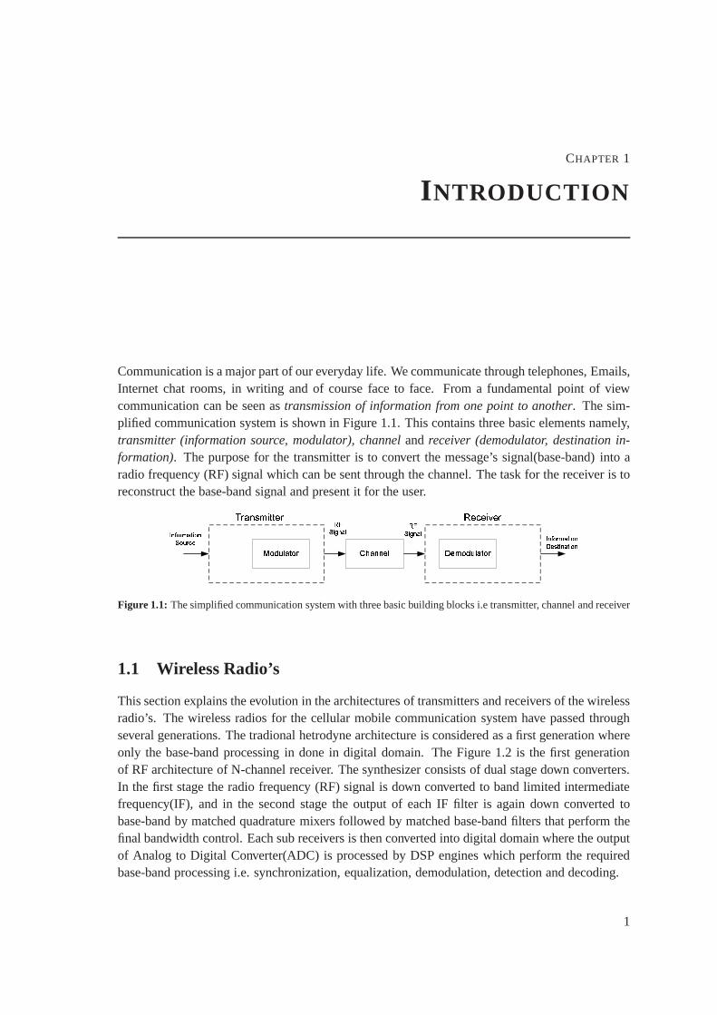
Communication is a major part of our everyday life. We communicate through telephones, Emails,Internet chat rooms, in writing and of course face to face. From a fundamental point of viewcommunication can be seen astransmission of information from one point to another. The sim-plified communication system is shown in Figure 1.1. This contains three basic elements namely,transmitter (information source, modulator), channeland receiver (demodulator, destination in-formation). The purpose for the transmitter is to convert the message’ssignal(base-band) into aradio frequency (RF) signal which can be sent through the channel. The task for the receiver is toreconstruct the base-band signal and present it for the user. ! " # $ % ! & % ' ! ! ( )" !* +( )" !* +, Figure 1.1: The simplified communication system with three basic building blocks i.e transmitter, channel and receiver
1.1 Wireless Radio’s
This section explains the evolution in the architectures oftransmitters and receivers of the wirelessradio’s. The wireless radios for the cellular mobile communication system have passed throughseveral generations. The tradional hetrodyne architecture is considered as a first generation whereonly the base-band processing in done in digital domain. TheFigure 1.2 is the first generationof RF architecture of N-channel receiver. The synthesizer consists of dual stage down converters.In the first stage the radio frequency (RF) signal is down converted to band limited intermediatefrequency(IF), and in the second stage the output of each IF filter is again down converted tobase-band by matched quadrature mixers followed by matchedbase-band filters that perform thefinal bandwidth control. Each sub receivers is then converted into digital domain where the outputof Analog to Digital Converter(ADC) is processed by DSP engines which perform the requiredbase-band processing i.e. synchronization, equalization, demodulation, detection and decoding.
1

Chapter 1 Introduction
.... .
.
.
.
Figure 1.2: A traditional radio receiver with multiple stage down conversion. There could possible be more than onedown-conversion in RF with single stage IF down-converter.Only the baseband processing is done in digital domain.
The problem with this type of architecture is that they have amplitude and phase imbalancewhich results in cross-talk between the narrow band channels due to ageing(time, temperature) ofanalog components of the quadrature down-converters, so each imbalance related spectral imagemust be lower then the desired spectral term, which is difficult to sustain over time and temper-ature. So the need to acheive the extreme levels of I/Q balance brings the second gereration ofradio’s which is shown in the Figure 1.3. In the second generation, the second stage(IF) downconversion is digitized, so for each sub-channel a digital down converter and a LPF is required.The digital conversion at IF brings more control on the imbalance by manipulating the number ofbits involved in the arithematic operation. The precision of coefficients used in the filtering pro-cess sets an upper bound to spectral artifacts levels at−5dB/bit, so the12bitADC will have animage level below−60dBs. Thus DSP based complex down conversion brings two advantages.First, the spectral images are controlled to be below the quantization noise floor of the ADC in-volved in the conversion process and second, the digital filter following and preceeding the mixersare designed to have linear phase characteristics [FredricJ. Harris and Rice, 2003]. This secondgeneation of wireless radio is a reliazable verion of software radio and is called ’Software DefinedRadio’.
!"#$% &' &() &*(+ , !"-+!"#$.,/0!"-+!"#$. ,/0%12 3
%12 42 !%12 42 5%12 625%12 62 !
7 &8 &(" * !"- + !"#$7 &8 &(" *9)7 &8 &(" *9) 7 &8 &(" * !"- + !"#$.
.
.
.
.
.
:) 3 759);<=Figure 1.3: The second generation of radio receiver, in which the IF stage becomes completely in digital domain. Thesecond generation bring control on the I/Q imbalance created by hardware oscillators.
2

1.1 Wireless Radio’s
1.1.1 Software Defined Radio
A software-defined radio (SDR) system is a radio communication system which can tune to anyfrequency band and receive any modulation across a large frequency spectrum by means of aprogrammable hardware which is controlled by software. An ideal software radio(ISR) samplesthe signal at RF, just after the antenna, whereas the realizable version of the software radio is theone that solve the problem of sampling the RF signal (according to minimum nyquits criteria, i.e.to sample at twice the maximum frequency of the incomming signal), by using a mixer and areference oscillator to heterodyne the radio signal to a lower frequency (Intermediate frequency),as described in the second generation of cellular radio’s, shown in Figure 1.3. In the Section 1.1,the architectural level significance of SDR is described, but there are lots of system level issues inthe wireless communication industry which embarks the essence and motivation for the SoftwareDefined Radio’s, which are:
• Commercial wireless network standards are continuously evolving from 2G to 2.5G/3G andthen further onto 4G. Each generation of networks differ significantly in link-layer protocolstandards causing problems to subscribers, wireless network operators and equipment ven-dors. Subscribers are forced to buy new handsets whenever a new generation of networkstandards is deployed. Wireless network operators face problems during migration of thenetwork from one generation to next due to presence of large number of subscribers usinglegacy handsets that may be incompatible with newer generation network.
• The air interface and link-layer protocols differ across various geographies (for e.g., Euro-pean wireless networks are predominantly GSM/TDMA based while in USA the wirelessnetworks are predominantly IS-95/CDMA2000 CDMA based). This problem has inhibitedthe deployment of global roaming facilities causing great inconvenience to subscribers whotravel frequently from one continent to another. Handset vendors face problems in buildingviable multi-mode handsets due to high cost and bulky natureof such handsets.
• Wireless network operators face deployment issues while rolling-out new services/featuresto realize new revenue-streams since this may require large-scale customizations on sub-scribers’ handsets.
SDR technology promises to solve these problems by implementing the radio functionality assoftware modules running on a generic hardware platform. Further, multiple software modulesimplementing different standards can be present in the radio system. The software modules thatimplement new services/features can be downloaded over-the-air onto the handsets. This kind offlexibility offered by SDR systems helps in dealing with problems due to differing standards andissues related to deployment of new services/features. There are lot of advantages of the full-downloadable type software radio, the system can be changedon demand by changing software,there are many gains for not only operators and service providers, but also for government andcommercial customers. such as, Global roaming services, bug fixed without the need to recall theproduct and new services can be added without changing the terminals [Ramjee Prasad, 2002].The most promising application of SDR is the application of cognitive radio (CR). The radio spec-trum becomes more and more sparse, making it an extensive task to allocate a new spectrum fornew services. The radio that is aware of its environment, internal state, and its location, then it
3
Chapter 1 Introduction
make a dicision about its operating behaviour based on that information [Cook, 2006].
1.2 Problem Description
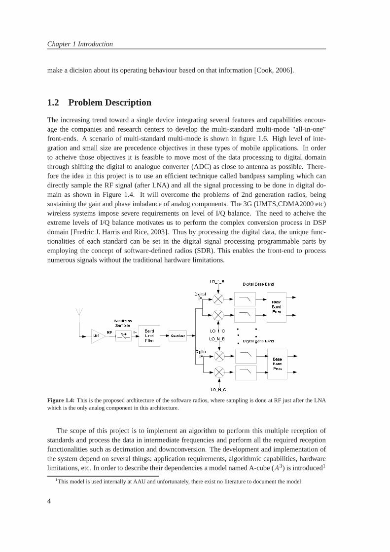
The increasing trend toward a single device integrating several features and capabilities encour-age the companies and research centers to develop the multi-standard multi-mode "all-in-one"front-ends. A scenario of multi-standard multi-mode is shown in figure 1.6. High level of inte-gration and small size are precedence objectives in these types of mobile applications. In orderto acheive those objectives it is feasible to move most of thedata processing to digital domainthrough shifting the digital to analogue converter (ADC) asclose to antenna as possible. There-fore the idea in this project is to use an efficient technique called bandpass sampling which candirectly sample the RF signal (after LNA) and all the signal processing to be done in digital do-main as shown in Figure 1.4. It will overcome the problems of 2nd generation radios, beingsustaining the gain and phase imbalance of analog components. The 3G (UMTS,CDMA2000 etc)wireless systems impose severe requirements on level of I/Qbalance. The need to acheive theextreme levels of I/Q balance motivates us to perform the complex conversion process in DSPdomain [Fredric J. Harris and Rice, 2003]. Thus by processing the digital data, the unique func-tionalities of each standard can be set in the digital signalprocessing programmable parts byemploying the concept of software-defined radios (SDR). This enables the front-end to processnumerous signals without the traditional hardware limitations.
.
.
.
.
.
.
!" # $ % & Figure 1.4: This is the proposed architecture of the software radios, where sampling is done at RF just after the LNAwhich is the only analog component in this architecture.
The scope of this project is to implement an algorithm to perform this multiple reception ofstandards and process the data in intermediate frequenciesand perform all the required receptionfunctionalities such as decimation and downconversion. The development and implementation ofthe system depend on several things: application requirements, algorithmic capabilities, hardwarelimitations, etc. In order to describe their dependencies amodel named A-cube (A3) is introduced1
1This model is used internally at AAU and unfortunately, there exist no literature to document the model
4

1.2 Problem Description
as shown in Figure 1.9. This model deals with two major parts,one being mapping from appli-cation to algorithm (algorithm development) and second mapping from algorithm to architecture(implementation). It is an iterative process, which means that we can go back and forth to tune theparameters of application, algorithm and architecture.
!"# Figure 1.5: The A3 model, used for illustrating the mapping from the application to the algorithm, and the mappingfrom algorithm to architecture. It is an iterative process.
1.2.1 Application
$ % & ' ( ) * + , -+ . / 0 1 2 ( ) * + , -+ .3 4 5 6 7 7 85 6 9 : ; < 9 4 ; ; 7 = 6 5 > > 5 ? <@ 8A ; 6 6A 3 B < C A <D 8B 4 E
= F G H6 I J KL M G N O P = 6 QFigure 1.6: A scenario of multi-standard multi-mode "all-in-one" front-ends user equipment. It highlights the userequipment capbale of receiving two standards i.e. UMTS and WLAN.
5

Chapter 1 Introduction
In the project, a multi-standard software radio reciever isconsidered. One of the main chal-langes is the coexistance of several standards in one user equipment(UE), since the chances forchannels interferance among the standards is very high [Behjou Nastaran, 2006]. Therefore, outof the multi-standards i.e. GPS, GSM, Bluetooth, zigbee, satellite communication, the applicationis limited to a case study where two standards being UMTS and WLAN are considered whichare shown in Figure 1.6, This is a case study which actually fits to the cellular systems where thepossible scenario could be that a doctor is talking with a patient on the mobile phone(UMTS) andat the same time it is down-loading the histroy of that patient(WLAN). Some of the specificationsof these standards are shown in Table 1.1 [Behjou Nastaran, 2006].
UMTS and WLAN Specifications for UEUMTS IEEE 802.11g
Duplexing FDD TDDFrequency Band 1920 - 1980 MHz: UL 2.4 - 2.4835 GHz
2110 - 2170 MHz: DLReceiver Sensitivity -117 dBm -82 to -65 dBmTransmitter Power Level 24 dBm (Class 3) 20 dBm (Europe)Channel Bandwidth 3.84 MHz 16.6 MHzNumber of non-overlapping channels 12 3
Table 1.1: Some specifications of UMTS and WLAN standards [Behjou Nastaran, 2006]
In the scenario of the project, the receiver must be able to receive the signals coming in alldifferent channels of these two standards. As mentioned in Table 1.1, the UMTS and WLAN sig-nal bands have 12 and 3 non-overlapping channels respectively. Thus, the target device must betune-able to serve to all different combinations of the two signals (36 different frequency combi-nations). we have to recieve only one of the possible combination out of them at a time.
1.2.2 Algorithm
The system level block diagram is shown in figure 4.2. The band-select filter is required to initiallyselect the whole band of information that contains both the standards i.e (UMTS and WLAN) andthen seperate them through a channel which have bandpass filters, and the block of channelizerwhich down convert and down-sample the IF signal to desired baseband along with the requiredchannels for each standard.
The algorithmic development for the design analysis of multiple standards have few phases.
• First, the idea is to use the aliases of the original signal atlower frequency(IF) while sampleit at higher frequency(RF). So the technique called ’bandpass sampling’ is used to acheivethe non-overlapped aliases of the WLAN and UMTS channels.
• Secondly, to design the digital band-select and bandpass filters at intermediate frequency(IF)(within the specification defined by first phase) to extract the relevent band within eachstandards.
• Finally, the channelizer is required to down-convert the IFsignals to baseband and to down-sample to the desired sampling frequency for both the UMTS and WLAN.
6

1.2 Problem Description
! " #
Figure 1.7: This is a complete block diagram of the system. After receiving the signal at antenna it is passed throughthe low noise amplifier(LNA) which boost-up the signal (adding a low noise). The next block is of bandpass samplingwhich samples the input at RF and brings the information downto IF. The band-select filter then select the completeband of interest followed by two channels which have individual BPF to seperate the multiple information, in this caseit is two i.e. UMTS and WLAN. followed by the block of channelizer which further down convert by down-samplingand filter the IF signal.
1.2.3 Architecture
The RF (Radio Frequency) front-end is supposed to receive two mentioned signals(UMTS,WLAN)at the same time. The signals are adjusted, filtered and consequently downconverted from RF tolower intermediate frequencies in the RF front-end design.After digitization, the signals arepassed through the digital signal processing block. The perspective of the project is to employ thestate of the art technology such as moderen DSPs or FPGA to process the data in intermediatefrequencies and perform all the required reception functionalities such as decimation and down-conversion.
$%&'()(*+ ,-.(%/%0)1-2+ 3+0('+.,-.(%3(&()-4 ,-.(%56789:;<9==>?@A:B=9CDEFFGHIJ KLMNOPQ RSTUVWX YQWZV[\ ]^[_SWZVZ[]_Z ]W SW `a S_QVWT_QSZVWX b\ S ^ST[]_ ]^[c] QdQ_\ ZQT]WY \QS_eFf FghGLiJjJhFGJFi Li klmnopmnpq
mnprmnpsmnptuvwx uvvx yxxx yxux zHLGJ
Figure 1.8: Gorden E. Moore Law: The number of transsitors are increasing by a factor of 2 after every 18 to 24months, due to increasing demand of applications. The complexity of the overall systems are increasing but with thedemands of minimum cost, minimum size, faster execution time and least power dissipation.
The selection of the hardware architecture is not easy for SDR based applications in an erawhere the number of transistors in an integrated circuit areincreasing by a factor of two every sec-ond year(Moor’s Law) as shown in the figure 1.8. As signal processing tasks (the algorithms) are
7
Chapter 1 Introduction
getting more and more complex which is at the same time putting high requirements on the tech-nologies platform with increasing demand of the MIPS(million of instructions per second). So thesoftware solution for SDR makes it possible to make the transition from dedicated, single-purposehardware (ASICs, etc.) to highly versatile general-purpose hardware such as FPGAs and DSPs,and even to general-purpose processors whose functionality is defined solely by their softwareconfiguration. This in turn paves the way for high-volume/low-cost production, making it finan-cially viable to embed autonomous radio communication devices in a wide range of new kindsof devices and applications [CSD, 2007]. The DSP is a specialized microprocessor optimized forperforming multiply and accumulate operations. The DSP hasalso proven to be inefficient forsome tasks, where a customized architecture actually is more suitable. One solution has been theapplication specific IC (ASIC), which is the least flexible, but most optimal solution with regardto execution time, power dissipation and cost. The cost factor is however, only low for a verylarge number of units, as the development of an ASIC is very expensive and time consuming.As the applications that request SDR based technology continue to require systems that can bereconfigured fast, as well as provide a massive amount of processing power, the need for powerfulreconfigurable architectures emerges. One solution for this is the use of field programmable gatearrays (FPGAs). FPGAs offer the possibility of programminglogic to be more suitable for certainalgorithms than the general DSP. This goes especially for algorithms where parallelism can be ex-ploited efficiently, but also more special operations like square root, cosine etc. are very suitablefor FPGA implementation. The use of FPGAs in handheld devices might be limited, as the costand power dissipation are still relatively high compared toan ASIC solution.
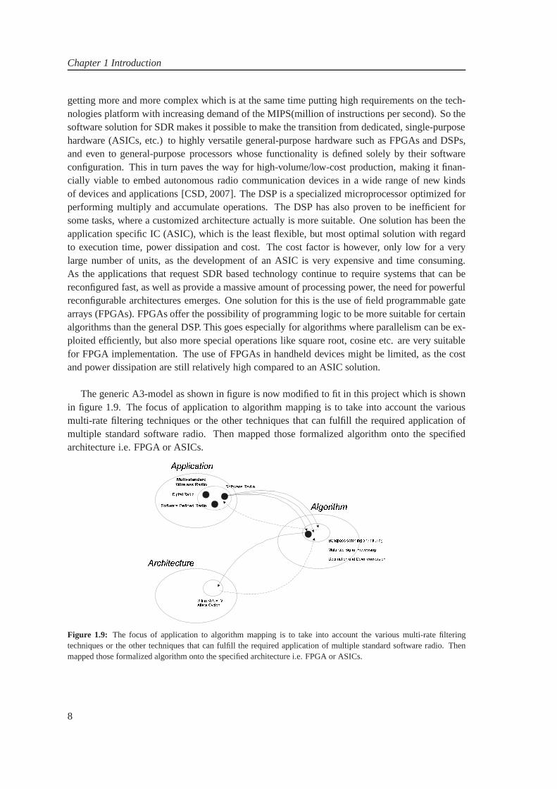
The generic A3-model as shown in figure is now modified to fit in this project which is shownin figure 1.9. The focus of application to algorithm mapping is to take into account the variousmulti-rate filtering techniques or the other techniques that can fulfill the required application ofmultiple standard software radio. Then mapped those formalized algorithm onto the specifiedarchitecture i.e. FPGA or ASICs.
! " #$$ % $&'( )(*+), -.$ ++/0123452678698:39;1;55 <683= >?@ABCDE FCGH?>?@ABCDE IE@HJEG FCGH?
Figure 1.9: The focus of application to algorithm mapping is to take intoaccount the various multi-rate filteringtechniques or the other techniques that can fulfill the required application of multiple standard software radio. Thenmapped those formalized algorithm onto the specified architecture i.e. FPGA or ASICs.
8
1.2 Problem Description
1.2.4 Problem Definition
Design analysis and implementation of Multi-standard Software Radio Receiver.
9


CHAPTER 2
SOFTWARE RADIO SYSTEM DESIGN
The principle idea behind the design of a software radio is toplace the analog-to-digital and digital-to-analog converters as near the antenna as possible, such that most of the radio functionalities canbe implemented on a programmable digital signal processor.One way to achieve this is by directbandpass sampling of the desired RF signal band to baseband frequency. However, the design ofa software radio receiver becomes more complicated when twoor more distinct RF signals are tobe received [Dennis M. Akos and Caschera, 1999].
In a multi-standard radio receiver design, UMTS and WLAN standards are taken as case studyand a receiver is required to receive both these standard simultaneously with same front-end, anddownconvert them to baseband separately. The spectral location for UMTS and WLAN standardsare shown in Figure 2.1. UMTS has a bandwidth of 60MHz for downlink having 12 channelsand WALN has a 84.5MHz of bandwidth having 3 channels. It is required to downsample and todownconvert these channels to baseband.
!" #$ %& '() * ++, %- & ., / 0, ' 12 3 " 45 6* 7Figure 2.1: Spectrum Allocation for UMTS and WLAN standards. UMTS has a bandwidth of 60MHz for downlinkhaving 12 channels and WALN has a 84.5MHz of bandwidth having3 channels.
2.1 Downconversion Techniques for Software Radio
Traditionally the superheterodyne architecture has been used extensively for radio systems sinceit provides a number of advantages such as image rejection and adjacent channel selectivity. Soft-ware radio is an enabling technology for future radio transceivers, allowing the realisation of mul-
11

Chapter 2 Software Radio System Design
timode, multiband, and reconfigurable base stations and terminals. Bandpass sampling and directconversion are two receiver architectures that are suitable for software radios. However, consider-able research efforts and breakthroughs in technology are required before the ideal software radiocan be realised.
2.1.1 Bandpass sampling Architecture
The sampling of bandpass signals can be carried out at rates lower than conventional lowpassNyquist sampling, causing intentional aliasing the signal. Bandpass sampling can allow for re-ceived signals to be digitized closer to the antenna using manageable sampling rates and hencecould be favourable for downconversion in software radios.In this project secnario, the totalreceiver bandwidth for the UMTS and the WLAN is 373.5MHz, as shown in the Figure 2.1. Ac-cording to bandpass sampling, the sampling frequency should be twice the signal bandwith ratherthan twice the maximum frequency component as in the case of Nyquist sampling. So the sam-pling frequency for the combined band of UMTS and WLAN must beatleast 747MHz to havenon-overlap alaises. Today’s technology set a limit to achieve such a high sampling rate. Signifi-cant improvement in ADC performance is required for sampling at RF.
! !
" # $ % & ' & ' ( # $ # ) * # " +, Figure 2.2: Bandpass sampling Architecture of Sofware Defined Radio
As the ADC is moved closer to the antenna, more radio functions can be written in softwareand embedded on programmable logic. However, ADC performance still is not sufficient enoughto perform digitization at RF [Patel and Lane, ]. In particular, the input analogue bandwidth, sam-pling rate, dynamic range and therefore resolution need considerable amounts of improvement ifwideband front-ends and sampling at RF are to become in a reality. The performance of DSPmust be able to cope with the increased amount of programmable radio functionality as a resultof moving the ADC closer to antenna. Schemes using a mixture of DSP and FPGA have beenproposed [Patel and Lane, ].
2.1.2 Direct Conversion Architecture
Direct conversion, also sometimes called zero-IF, due to the lack of an intermediate frequency,converts the received RF signal direct to baseband. This is particularly attractive for the use inwireless systems, especially in handsets since direct conversion receivers lend themselves more
12

2.1 Downconversion Techniques for Software Radio
easily to monolithic integration than heterodyne architectures, since the IF components are re-placed by lowpass filters and baseband amplifiers. Direct conversion exhibits immunity to theproblem of image since there is no IF [Patel and Lane, ]. Thereare a number of design issuesassociated with the direct conversion architecture. The most serious problem is DC offset in thebaseband, following the mixer. This offset appears in the middle of the downconverted signal spec-trum, and may be larger than the signal itself. This phenomenon can be caused by local oscillatorleakage and self-mixing [Patel and Lane, ]. ! " # $ % & ' (# ) * $ % & ' ( +
+ , - . / 0 1 Figure 2.3: Direct conversion Architecture of Sofware Defined Radio
Bandpass sampling allows for the ADC to digitize at RF, providing the ADC is of adequate per-formance, whereas direct conversion, although consistingof more analogue components, placesfewer demands on ADC performance since digitization occursat baseband.
As mentioned above that by moving the ADC closer to the antenna, more radio functions canbe written in software and embedded on programmable logic. Sampling at the antenna is notrealistic since some amount of band select and filtering mustoccur prior to the ADC to minimizeadjacent channel issues. However, sampling at the First-IFis practical, yeilding the concept ofDirect-IF sampling.
2.1.3 Direct-IF Sampling Architecture
Recent advances in converter technology have allowed data converters to faithfully sample analogsignals as high as several hundred MHz. Sample rates need only be as high as twice the signalbandwidth to keep the Nyquist principle. Since most air interface standards are less than a fewhundred MHz wide, sample rates in the tens of MHz are required, eliminating the need for ex-tremely fast sample rates in radio design. Thus allowing forlow cost digitizers [Brannon, ]. AIF-sampling radio receiver is shown in Figure 2.4.
Once digitized, the signal would have to be processed. With atypical sample rate of 20 MHz(for instance), data would stream too fast for even the hottest DSP to do much with in terms offiltering, much less process the data for user information. Therefore, some preprocessing of thedata must occur [Brannon, ]. With a sample rate of 20 MHz, the data bandwidth would be 10MHz, much more than is needed for most air interfaces. Therefore, one thing that preprocessingshould achieve is to reduce the data bandwidth as well as the data rate. Thus in addition to theADC (analog-to-digital converter) a DSP preprocessor is required as shown in Figure 2.5.
13

Chapter 2 Software Radio System Design
! Figure 2.4: Direct IF sampling software Defined Radio
" # $ % & '( " ) # * " + +, - . / 0 1 ( " ) # * " + +, - . / 0 1( " ) # * " + +, - . / 0 1# 0 $ - 2 " / 3 1# 0 $ - 2 " / 3 1
4 5 & 6 7 8 9 : ; <4 ; = > ? @ 6 A > & > A = : B ; ( C D E F C G H* I J K E D D L G M
Figure 2.5: Interface circuit required between IF-sampling and baseband processing
2.2 Architecture Selection
In the above section, different architectures have been discussed in terms of their performance andstructures. The project aim is to have multi-standard receiver where the ADC is place as closeto the antenna as possible. The Direct-IF sampling uses downconversion process prior to ADCconversion. This leaves the other two possible arhitecturei.e bandpass sampling and direct con-version for the consideration. Bandpass sampling architecture does not require additional circuitsfor downconversion prior to quantization. This leads to allthe processing required for bandpasssampling architecture to be implemented on FPGA which can bereconfigured to different radioconfiguration. Although the choice of ADC becomes more critical, but we will not deal with theseissues.
The project focuses on the bandpass sampling architecture.We deal only with the sampled dataafter the ADC process. It is required to downconvert and downsample the individual channels ofUMTS and WLAN standards to baseband.
2.3 Design Process
Bandpass sampling architecture has been selected as discussed in the previous section. This leadsto the selection of sampling frequency which is critical. A sampling frequncy of 676MHz is takenas a start [Behjou Nastaran, 2006]. This frequency is below the required sampling of 747MHz,in order to have non-overlap aliases. In the combined spectrum for UMTS and WLAN, there
14

2.3 Design Process
is an unsed spectrum between them. By having the overlap aliases in this unused spectrum, thesampling frequency can be decreased. This is the case for thesampling frequency at 676MHz asshown in Figure 2.6.
! "# $! % ! & $ '(" ) * + , - ./ 0. 1 23/ 0.4 5 3 26 078 6 - ./ - 9/ 8 :; < = > ? @ A+ B C 08 3 ./ D 98 - 5 E 2D / F G H G < I J - ./ 6 K D B L M 3 08 6N 9D M 3D . 1 L , - ./ : 7O O P < I J C 1 Q .6 - 0. 8 6 K D - 20- 8 D 8 Q N 6 K D 8 6 - ./ - 9/ 8 04 . - 28 R = K D - 2 0- 8 D 8 Q N 6 K D 9D 1 D 0S 0.4 , - ./ - 9D Q S D 9 2- E E D /, 36 - 20- 8 D 8 NQ 9 0./ 0S 0/ 3 - 2 8 6 - ./ - 9/ , - ./ 8 - 9D 8 6 022 . Q .7Q S D 9 2- E ED / R = K D @ A+ B ,D 1 Q 5 D 8 8 E D 1 6 9- 22L 0.S D 96D / 0. 6 K D B M 3 08 6N 9D M 3 . 1 L J Q . D R T U V W X YZ [Z \]^ _ ` aT U V W Z \]^ _ ` aX YZ [[ b c d ]_ ef g` c d ` h i bj k h `
Figure 2.6: Combined spectrum of UMTS and WLAN is bandpass sampled at 676MHz. 12 channels of UMTS arerequired to downsample from 676MHz to 61.44MHz, and 3 channels of WLAN are required to downsample from676MHz to 20MHz, along with downconversion to base band.
The combined spectrum is aliased to Nyquist-zone (fs/2) as overlap aliases but the requiredUMTS and WLAN bands are still non-overlapped. The zoom of spectrum in the Nyquist-zone isshown in the Figure 2.7.
l l mn o p q o o o r s r qtu v o o o
w o r rp x rp r r o x r s r rx r s x r yz | ~ w ¡ ¢£ ¤ ¡ ¢£ ¤
Figure 2.7: The zoom of spectrum in the Nyquist-zone. The resulted aliased signals for UMTS and WLAN lie at(82-142)MHz and (220-304)MHz respectively.
The individual channels (12 UMTS channels and 3 WLAN channels) are shown in Figure 2.8.Each of UMTS channel is 5MHz wide and have 5MHz of spacing between inter-channel carriers,whereas each of the WLAN channel is 24MHz wide and have 30MHz of spacing between inter-channel carriers.
The resulted aliased signals for UMTS and WLAN lie at (82-142)MHz and (220-304)MHzrespectively. The goal is to downsample these signals to thedesired rate i.e. 20MHz for WLANand16 × 3.84 = 61.44MHz for UMTS. 3.84 is the UMTS bandwidth and the number16 is theoversampled ratio that can vary as 16, 32, etc. But the number16 has been taken into account.The required sample rates for UMTS and WLAN are summaried in the Table 2.1.
15

Chapter 2 Software Radio System Design ! " # # $ $ % & ' ( ) * + ,- . " # " / & ' ( ) " 01 " $ % 2 ' 3 4 5 # $" ! 6 7 $ 6 # 7 8 5 " + ,- . " 9 " $ % 1 : ' 3 4 5 # ; ' 3 4 $ % " ! 6 7 $ 6 < " /
= = = = => ? @> ? A > ? AB > ? AC $ % # & ' ( ) " # $ < $5 " 7 ! % $ 7; D ; ' 3 4 #$ ; 0 /: : ' 3 4 $5 $ # # $ < " < " 5 E " " $5 < $ F C $ % # + ,- . " # $ < $5 " 7 ! % $ 7; D ; ' 34 #$ 1 G ' 3 4 $5 $ # #$ < " < "5 E " " $5 <$ FH I J K L M NO O P Q R H I J K S T P Q R> ? B => ? B => ? @Figure 2.8: Individual channels: (12 UMTS channels and 3 WLAN channels). Each of UMTS channel is 5MHz wideand have 5MHz of spacing between inter-channel carriers, whereas each of the WLAN channel is 24MHz wide andhave 30MHz of spacing between inter-channel carriers.
Specifications for UMTS and WLAN sample ratesStandards Current sampling rate (MHz) Desired Sampling rate (MHz)UMTS 676 61.44WLAN 676 20
Table 2.1: Specifications for UMTS and WLAN sample rates.
In order to extract these channels and downconvert them to baseband at the required rates,channelizers are required, which will be explained in the next section.
2.4 Channelization
A conventional way to do channelization is presented in the Figure 2.9, where each channel is firstdownconverted to baseband and then downsampled after passing through a lowpass filter.U VWX YZ [\ ]^_ U VWX YZ [\ ] `_
U VWX YZ [\ ]a_ U VWX YZ [\ ]b c`_def gh ii jklmn odef gh ii jklmn odef gh ii jklmn odef gh ii jklmn ophq g ln r r h mh sth uun l vsth uun l wsth u un l xs th uun l y z w
Figure 2.9: Conventional channelization: where each channel is first downconverted to baseband and then downsam-pled after passing through a lowpass filter.
16

2.4 Channelization
The digital sample rate conversion uses the techniques suchas decimation, interpolation andcombination of them to have rate conversion by rational numbers. In a process of decimation byM , M − 1 samples are discarded and every Mth sample is taken in to account. This results in thespectral expansion, so the bandwith of the signal is first reduced before the decimation process tocompensate this expansion. The general system for decimation is shown in Figure 2.10. !" # $% & ' () *" ' + ,- .
Figure 2.10: General system for sampling rate reduction by facor M [Alan V. Oppenheim, 1999].
On the other hand, in a process of interpolation byM , M − 1 zeros are inserted between thesamples. It results in the aliases at the multiple of the output frequency which are removed byusing a lowpass filter after the interpolation process. The zero insertion also results in decrease inthe average signal energy, which is compensated by the gain of the filter. The general system forinterpolation is shown in Figure 2.11. These processes are explained in detail in Appendix A./ 0 12 34 50 34 56 7 8 9 :;< =9 > ? ;@ A B 6 7 8 9 : ;< = 9 > ? ;@ AB CD B E F G HI J K L L M NOP Q RS K NT U GV WP H M M U X YZ0 2 34 5 6 7 8 9 :;< = 9 > ? ;@ AB CD B E F
Figure 2.11: General system for sampling rate increase by facor L [Alan V.Oppenheim, 1999]
There are some of the observation in the conventional channelizer, which are listed below:
• The rate conversion process is carried out after downconversion and passing through thefilter, which simply discards the samples processed by the downconverter and filter(in thecase of decimator). There is no need to process the samples which are eventually discardedby the down sample operation. This will result in the significant computational savings.
• Rate changes by large factor, requires a long filter which results in an increase in computa-tional complexity. One of the solutions is to have multi-stage operations.
• The downconversion and the filter operate at the same rate as the input sampling frequency.
Based on the above observations, there should be some efficient channelizer structure. An ef-ficient structure performs the channelization as a single merged process called a polyphase-pathfilter bank, which is shown in Figure 2.12. The polyphase filter bank partition offers a numberof significant advantages relative to the set of individual down-conversion receivers. The primaryadvantage is reduced cost due to major reduction in system resources required to perform the mul-tichannel processing [Fredric J. Harris and Rice, 2003]. The next section describes the polyphasechannelization in detail.
17

Chapter 2 Software Radio System Design
! " #! " # $ % &' Figure 2.12: Polyphase channelizer: resampler, all-pas partition, andFFT phase shifters
2.5 Polyphase Channelization
In conventional channelizer as shown in Figure 2.9, individual channelizer for each channel arerequired. One can form only one channel and by having reconfigurability of that, can be used forother channels. On the other hand, the channelizer proposedby ’Fredric J. Harris’ as shown inFigure 2.12 is capable of delivering all the required channels just by using one channelizer. Be-sides that it is more efficient when large sampling rate changes are required.
In the understanding of polyphase channelizer, a stepwise process is explained now, startingfrom the conventional channelizer and transforming it to the polyphase channelizer [Fredric J. Harris and Rice, 2003].The block diagram of a single channel of a conventional channelizer is shown in Figure2.13. Thisstructure performs the standard operations of down conversion of the selected channel with acomplex heterodyne, low-pass filtering to reduce bandwidthto the channel bandwidth, and downsampling to a reduced rate commensurate with the reduced bandwidth.
( ) * + ,- . / 0 1 2 3 4 5 46 7 89 : ; < 7 = = > 4 8 6 ? @A B C D E B C F G D E B C , F G DFigure 2.13: Kth channel of conventional channelizer
The expression fory(n, k), the time series output from the kth channel, prior to resampling, isa simple convolution, as shown in the following:
y(n, k) = [x[n]e−jθkn] ∗ h[n] (2.1)
=
N−1∑
r=0
x[n − r]e−jθk(n−r)h[r] (2.2)
The summation of Equation 2.2 can be rearranged to obtain a related summation reflectingthe equivalency theorem. The equivalency theorem states that the operations of down conversion
18

2.5 Polyphase Channelization
followed by a low-pass filter are totally equivalent to the operations of a bandpass filter followedby a down conversion.
y(n, k) =
N−1∑
r=0
x[n − r]e−jθk(n−r)h[r] (2.3)
=
N−1∑
r=0
x[n − r]e−jnθkh[r]ejrθk (2.4)
= e−jnθk
N−1∑
r=0
x[n − r]h[r]ejrθk (2.5)
The block diagram demonstrating this relationship is shownin Figure 2.14, while the rear-ranged version of Equation 2.2 is shown in Equation 2.5. ! !
Figure 2.14: Bandpass filter, Kth channel of channelizer
Applying the transformation suggested by the equivalency theorem to an analog prototype sys-tem does not make sense since it doubles the required hardware. It would have to replace a com-plex scalar heterodyne (two mixers) and a pair of low-pass filters with a pair of bandpass filters,containing twice the number of reactive components, and a full complex heterodyne (four mixers),whereas digital filters which are defined as a set of weights stored in coefficient memory. So, inthe digital world, no cost is incurred in replacing the low-pass filter required in the first option withbandpass filter required for the second option. This is accomplished by a simple download to thecoefficient memory.
It is noted that following the output down conversion, a sample rate reduction is performed byretaining only one sample in everyM samples. Recognizing that there is no need to down convertthe samples that are discarded in the down sample operation,so only the retained samples are tobe down sampled. This is shown in Figure 2.15." # $ % & ' ( ) * + , & ' + ( - ./ 01 02 3 45 3 6 7 8 9 3 : : ; 0 4 2 < => ? @ A B ? @ + C D A
Figure 2.15: Down-sampled down-converted bandpass kth channel of channelizer
The down converter is shifted to the low data-rate side of theresampler, it is, in fact, also downsampling the time series of the complex sinusoid. The rotation rate of the sampled complex si-nusoid isΘk andMΘk radians per sample at the input and output, respectively, ofthe M-to-1
19
Chapter 2 Software Radio System Design
resampler.
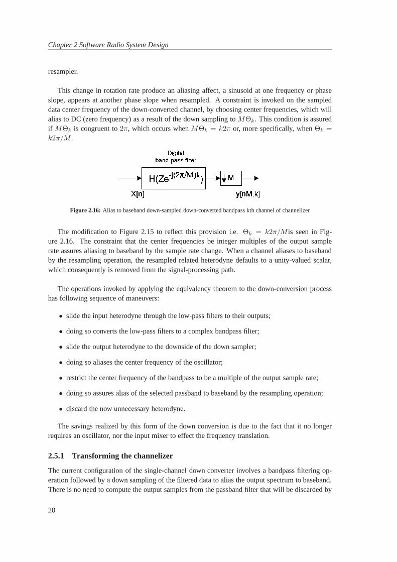
This change in rotation rate produce an aliasing affect, a sinusoid at one frequency or phaseslope, appears at another phase slope when resampled. A constraint is invoked on the sampleddata center frequency of the down-converted channel, by choosing center frequencies, which willalias to DC (zero frequency) as a result of the down sampling to MΘk. This condition is assuredif MΘk is congruent to2π, which occurs whenMΘk = k2π or, more specifically, whenΘk =
k2π/M . ! " # $ !Figure 2.16: Alias to baseband down-sampled down-converted bandpass kth channel of channelizer
The modification to Figure 2.15 to reflect this provision i.e.Θk = k2π/M is seen in Fig-ure 2.16. The constraint that the center frequencies be integer multiples of the output samplerate assures aliasing to baseband by the sample rate change.When a channel aliases to basebandby the resampling operation, the resampled related heterodyne defaults to a unity-valued scalar,which consequently is removed from the signal-processing path.
The operations invoked by applying the equivalency theoremto the down-conversion processhas following sequence of maneuvers:
• slide the input heterodyne through the low-pass filters to their outputs;
• doing so converts the low-pass filters to a complex bandpass filter;
• slide the output heterodyne to the downside of the down sampler;
• doing so aliases the center frequency of the oscillator;
• restrict the center frequency of the bandpass to be a multiple of the output sample rate;
• doing so assures alias of the selected passband to baseband by the resampling operation;
• discard the now unnecessary heterodyne.
The savings realized by this form of the down conversion is due to the fact that it no longerrequires an oscillator, nor the input mixer to effect the frequency translation.
2.5.1 Transforming the channelizer
The current configuration of the single-channel down converter involves a bandpass filtering op-eration followed by a down sampling of the filtered data to alias the output spectrum to baseband.There is no need to compute the output samples from the passband filter that will be discarded by
20
2.5 Polyphase Channelization
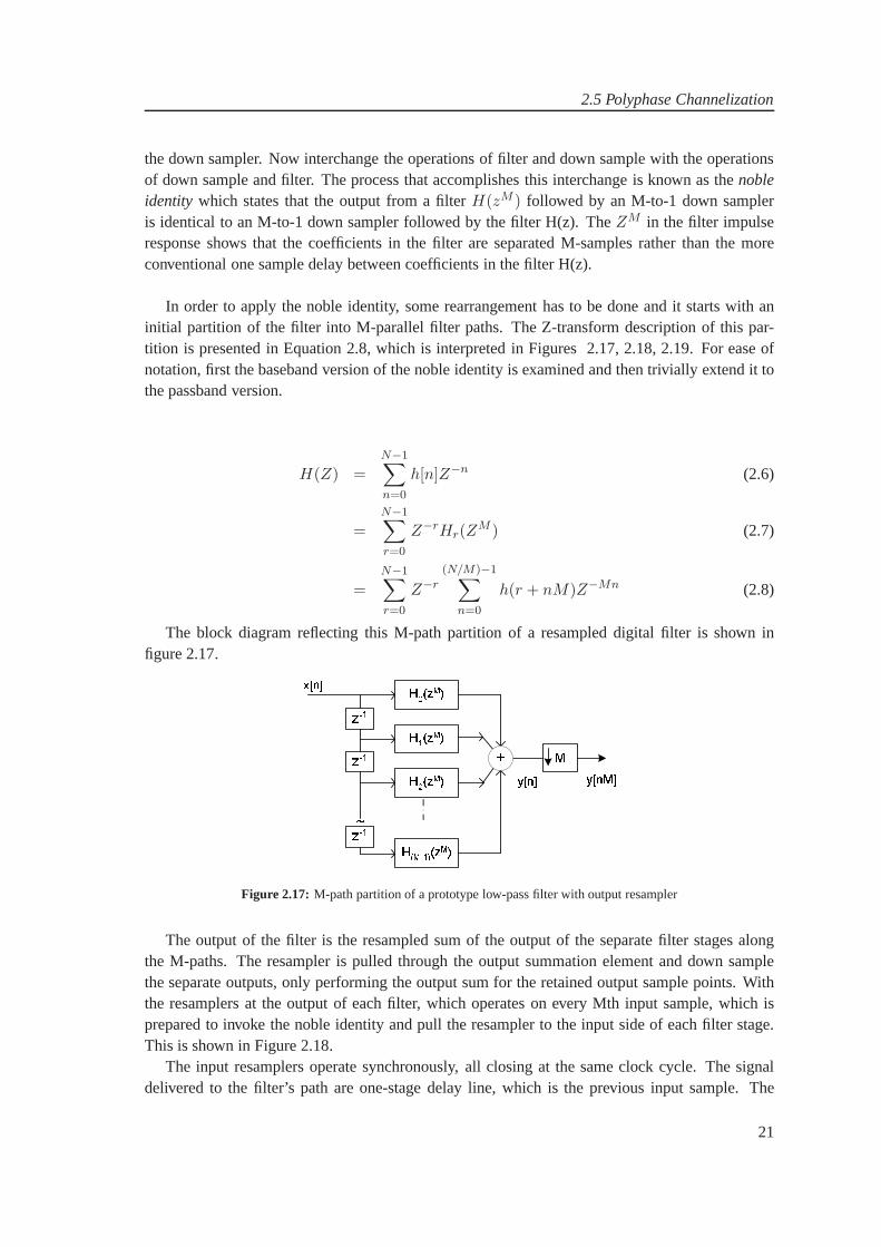
the down sampler. Now interchange the operations of filter and down sample with the operationsof down sample and filter. The process that accomplishes thisinterchange is known as thenobleidentity which states that the output from a filterH(zM ) followed by an M-to-1 down sampleris identical to an M-to-1 down sampler followed by the filter H(z). TheZM in the filter impulseresponse shows that the coefficients in the filter are separated M-samples rather than the moreconventional one sample delay between coefficients in the filter H(z).
In order to apply the noble identity, some rearrangement hasto be done and it starts with aninitial partition of the filter into M-parallel filter paths.The Z-transform description of this par-tition is presented in Equation 2.8, which is interpreted inFigures 2.17, 2.18, 2.19. For ease ofnotation, first the baseband version of the noble identity isexamined and then trivially extend it tothe passband version.
H(Z) =
N−1∑
n=0
h[n]Z−n (2.6)
=N−1∑
r=0
Z−rHr(ZM ) (2.7)
=
N−1∑
r=0
Z−r
(N/M)−1∑
n=0
h(r + nM)Z−Mn (2.8)
The block diagram reflecting this M-path partition of a resampled digital filter is shown infigure 2.17.
Figure 2.17: M-path partition of a prototype low-pass filter with output resampler
The output of the filter is the resampled sum of the output of the separate filter stages alongthe M-paths. The resampler is pulled through the output summation element and down samplethe separate outputs, only performing the output sum for theretained output sample points. Withthe resamplers at the output of each filter, which operates onevery Mth input sample, which isprepared to invoke the noble identity and pull the resamplerto the input side of each filter stage.This is shown in Figure 2.18.
The input resamplers operate synchronously, all closing atthe same clock cycle. The signaldelivered to the filter’s path are one-stage delay line, which is the previous input sample. The
21

Chapter 2 Software Radio System Design
Figure 2.18: M-path partition of a prototype low-pass filter with input resampler (Noble Identity)
interaction of the delay lines in each path with the set of synchronous switches(M-1 converters)can be likened to an input commutator that delivers successive samples to successive legs of theM-path filter. This interpretation is shown in Figure 2.19.
! " # $ % & '
Figure 2.19: M-path partition of a prototype low-pass filter with input path delays and M-1 resamplers replaced byinput commutator.
Now the final steps of the transform is carried out that changes a standard mixer down converterto a resampling M-path down converter. By applying the frequency translation property of theZ-transform, a low-pass filter can be converted to a bandpassfilter by associating the complexheterodyne terms of the modulation process either with the filter weights or with the delay elementsstoring the filter weights.
H(Z) =
N−1∑
n=0
h[n]Z−n (2.9)
G(Z) = H(Z)|z=ejθZ = H(e−jθZ) (2.10)
Now applying this relationship to Equation 2.5 or, equivalently, to Figure 2.19 by replacingeachZ with Ze−jθ, or more clearly, replacing eachZ−1 with Z−1ejθ, with the phase term sat-isfying the congruency constraint thatθ = k(2π/M). Thus,Z−1 is replaced withZ−1ejk(2π/M),andZ−M is replaced withZ−MejkM(2π/M). By design, the kMth multiple of2π/M is a multiple
22

2.5 Polyphase Channelization
of 2π for which the complex phase rotator term defaults to unity, or in this interpretation, aliasesto baseband (dc). The default to unity of the complex phase rotator occurs in each path of theM-path filter shown in Figure 2.20. The nondefault complex phase angles are attached to the de-lay elements on each of the M paths. For these delays, the terms Z−rare replaced by the termsZ−rejkr(2π/M). The complex scalar attached to each path of the M-path filtercan be placed any-where along the path and, in anticipation of the next step, the complex scalar are placed after thedown-sampled path filter segmentsHr(Z). This is shown in Figure 2.20. ! " #$% & '( )*
Figure 2.20: Re-sampling M-path down converter
The modification to the original partitioned Z-transform ofEquation 2.8 to reflect the addedphase rotators of Figure 2.20 is shown in the following:
H(Ze−j(2π/M)k) =M−1∑
r=0
Z−rej(2π/M)rkHr(Z) (2.11)
The computation of the time series obtained from the output summation in Figure 2.20 is shownin Equation 2.12.
y(nM, k) =
M−1∑
r=0
yr(nM)ej(2π/M)rk (2.12)
Here, the argumentnM reflects the down-sampling operation, which increments through thetime index in stride of lengthM , delivering everyM th sample of the original output series. Thevariableyr(nM) is thenM th sample from the filter segment in therth path, andy(nM, k) is thenM th time sample of the time series from thekth center frequency. The down-converted centerfrequencies located at integer multiples of the output sample frequency are the frequencies thatalias to zero frequency under the resampling operation. Note the outputy(nM, k) is computed asa phase coherent summation of theM output seriesyr(nM). This phase coherent sum is, in fact,a discrete Fourier transform (DFT) of the M-path outputs, which can be likened to beam formingthe output of the path filters.
The beam-forming perspective offers an interesting insight to the operation of the resampleddown-converter system. The reasoning proceeds as follows:the commutator delivering consecu-tive samples to the M input ports of the M-path filter performsa down-sampling operation. Each
23
Chapter 2 Software Radio System Design
port of the M-path filter receives data at oneM th of the input rate. The down sampling causes theM-to-1 spectral folding, effectively translating the M-multiples of the output sample rate to base-band. The alias terms in each path of the M-path filter exhibitunique phase profiles due to theirdistinct center frequencies and the time offsets of the different down-sampled time series deliveredto each port. These time offset are, in fact, the input delaysshown in Figure 2.18 and in Equa-tion 2.13. Each of the aliased center frequency experiencesa phase shift shown in Equation 2.13equal to the product of its center frequency and the path timedelay.
φ(r, k) = ωk∆Tr = 2π(fs/M)krTs = 2π(fs/M)kr(1/fs) = (2π/M)kr (2.13)
The phase shifters of the DFT perform phase coherent summation, very much like that per-formed in narrow-band beam forming, extracting from the myriad of aliased time series, the aliaswith the particular matching phase profile. This phase-sensitive summation aligns contributionsfrom the desired alias to realize the processing gain of the coherent sum while the remaining aliasterms, which exhibit rotation rates corresponding to the M roots of unity, are destructively can-celed in the summation.
The inputs to the M-path filter are not narrow-band, and phaseshift alone is insufficient toeffect the destructive cancellation over the full bandwidth of the undesired spectral contributions.To successfully separate wide-band signals with unique phase profiles due to the input commuta-tor delays, the operation equivalent of time-delay beam forming must be performed. The M-pathfilters, obtained by M-to-1 down sampling of the prototype low-pass filter supply the requiredtime delays. The M-path filters are approximations to all-pass filters, exhibiting, over the channelbandwidth, equal ripple approximation to unity gain and theset of linear phase shifts that providethe time delays required for the time-delay beam-forming task.
A useful perspective is that the phase rotators following the filters perform phase alignmentof the band center for each aliased spectral band while the polyphase filters perform the requireddifferential phase shift across these same channel bandwidths. When the polyphase filter is usedto down convert and down sample a single channel, the phase rotators are implemented as ex-ternal complex products following each path filter. When a small number of channels are beingdown converted and down sampled, appropriate sets of phase rotators can be applied to the filterstage outputs and summed to form each channel output. When the number of channels becomessufficiently large in the order oflog2(N), the DFT operation can be used to simultaneously ap-ply the phase shifters for all of the channels required to extract from the aliased signal set. Forcomputational efficiency, the FFT algorithm is used to implement the DFT.
2.5.2 Summary
The commutator performs an input sample rate reduction by commutating successive input sam-ples to selected paths of the M-path filter. Sample rate reduction occurring prior to any signalprocessing causes spectral regions residing at multiples of the output sample rate to alias to base-band. This desired result allows to replace the many down converters of a standard channelizer,implemented with dual mixers, quadrature oscillators, andbandwidth reducing filters, with a col-
24
2.6 Polyphase filter bank parameters
lection of trivial aliasing operations performed in a single partitioned and resampled filter.
The partitioned M-path filter performs the task of aligning the time origins of the offset sampleddata sequences delivered by the input commutator to a singlecommon output time origin. This isaccomplished by the all-pass characteristics of the M-pathfilter sections that apply the requireddifferential time delay to the individual input time series. The DFT performs the equivalent ofa beam-forming operation; the coherent summation of the time-aligned signals at each outputport with selected phase profiles. The phase coherent summation of the outputs of the M-pathfilters separate the various aliases residing in each path byconstructively summing the selectedaliased frequency components located in each path, while simultaneously destructively cancelingthe remaining aliased spectral components.
2.6 Polyphase filter bank parameters
Channel bandwidth, spectral spacingand theoutput sampling rates are the parameters, re-quired to be adjusted for the polyphase channelizer. The DFTperforms the task of separat-ing the channels after the polyphase filter so it is natural toconclude that the transform size islocked to the number of channels [Fredric J. Harris and Rice,2003]. Filter bandwidth is deter-mined by the weights of the low-pass prototype and that this bandwidth and spectral shape iscommon to all the channels. In standard channelizer designs, the bandwidth of the prototype isspecified in accord with the end use of the channelizer outputs. when a channelizer is used toseparate adjacent communication channels, which are characterized by known center frequenciesand known controlled nonoverlapping bandwidths, the channelizer must preserve separation ofthe channel outputs. Inadequate adjacent channel separation results in adjacent channel interfer-ence [Fredric J. Harris and Rice, 2003].
The polyphase filter channelizer uses the input M-to-1 resampling to alias the spectral termsresiding at multiples of the output sample rate to baseband.This means that, for the standardpolyphase channelizer, the output sample rate is the same asthe channel spacing. When operatedin this mode, the system is called amaximally decimated filter bank.
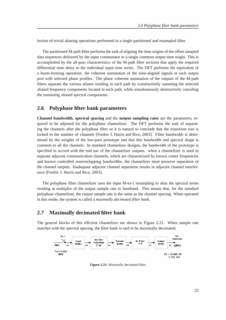
2.7 Maximally decimated filter bank
The general blocks of this efficient channelizer are shown inFigure 2.21. When sample ratematches with the spectral spacing, the filter bank is said to be maximally decimated. ! " # $ # $ # $ # $ # $ % & ' ( ) * + ! " , # $
Figure 2.21: Maximally decimated filter
25
Chapter 2 Software Radio System Design
Figure 2.21 shows a system in which a sequence atfs is downsampled by a factor ofM = 64
and fed to a 64-path polyphase filter. The commutator performs an input sample rate reduction bycommutating successive input samples to selected paths of the M-path filter. The down-sampler- acommutator operating at a rate of M (64), is an efficient implementation of down-sampler, insteadof using delay elements and then 64-1 (M-1) down-samplers for each polyphase path.
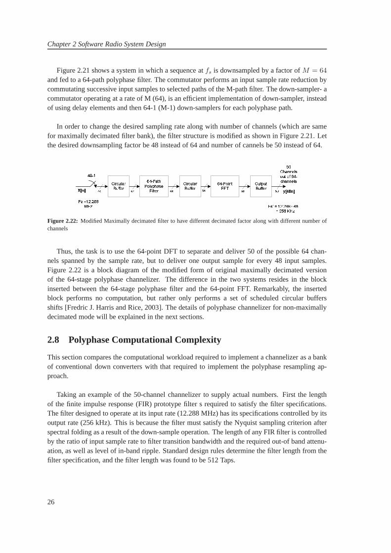
In order to change the desired sampling rate along with number of channels (which are samefor maximally decimated filter bank), the filter structure ismodified as shown in Figure 2.21. Letthe desired downsampling factor be 48 instead of 64 and number of cannels be 50 instead of 64. ! " # $ % $ % $ % & ' & ' ( ) * + , - . " #
- / % 0Figure 2.22: Modified Maximally decimated filter to have different decimated factor along with different number ofchannels
Thus, the task is to use the 64-point DFT to separate and deliver 50 of the possible 64 chan-nels spanned by the sample rate, but to deliver one output sample for every 48 input samples.Figure 2.22 is a block diagram of the modified form of originalmaximally decimated versionof the 64-stage polyphase channelizer. The difference in the two systems resides in the blockinserted between the 64-stage polyphase filter and the 64-point FFT. Remarkably, the insertedblock performs no computation, but rather only performs a set of scheduled circular buffersshifts [Fredric J. Harris and Rice, 2003]. The details of polyphase channelizer for non-maximallydecimated mode will be explained in the next sections.
2.8 Polyphase Computational Complexity
This section compares the computational workload requiredto implement a channelizer as a bankof conventional down converters with that required to implement the polyphase resampling ap-proach.
Taking an example of the 50-channel channelizer to supply actual numbers. First the lengthof the finite impulse response (FIR) prototype filter s required to satisfy the filter specifications.The filter designed to operate at its input rate (12.288 MHz) has its specifications controlled by itsoutput rate (256 kHz). This is because the filter must satisfythe Nyquist sampling criterion afterspectral folding as a result of the down-sample operation. The length of any FIR filter is controlledby the ratio of input sample rate to filter transition bandwidth and the required out-of band attenu-ation, as well as level of in-band ripple. Standard design rules determine the filter length from thefilter specification, and the filter length was found to be 512 Taps.
26

2.8 Polyphase Computational Complexity
An important consideration and perspective for filters thathave different input and output sam-ple rates is the ratio of filter length (with units of operations/output) to resample ratio (with units ofinputs/output) to obtain the filter workload (with units of operations/input) [Fredric J. Harris and Rice, 2003].A useful comparison of two processes is the number of multiplies and adds per input point. A mul-tiply and add with their requisite data and coefficient fetchcycles is counted as a single processoroperation and uses the shorthand notation of "ops" per input.
A single channel of a standard down-converter channelizer requires one complex multiply perinput point for the input heterodyne and computes one complex output from the pair of 512 tapfilters after collecting 48 inputs from the heterodyne. The four real ops per input for the mixer andthe two (512/48) ops per input for the filter result in a per channel workload of 26 ops per input,which occur at the input sample rate [Fredric J. Harris and Rice, 2003].
The polyphase version of the down converter collects 48 input samples from the input commu-tator, performs 1024 ops in the pair of 512 tap filters, and then performs a 64-point FFT with itsupper bound workload of real ops. The total workload of 1024 ops for the filter and 768 ops for theFFT results in 1792 ops performed once per 48 inputs for an input workload of 38 real ops/input.The higher workload per input is the consequence of forming 64 output channels in the FFT, butpreserving only 50 of them [Fredric J. Harris and Rice, 2003].
The workload per input sample for the standard channelizer was found to be 26 ops, and forthe polyphase channelizer was found to be 38 ops. The advantage is that the polyphase 38 opsper input built all 50 channels, and the standard down converter’s 26 ops per input built only onechannel and has to be repeated 50 times. Thats impressive!. By comparing numbers, it can beconcluded that the polyphase form should be used even if justa few output channels are required,because the polyphase down converter requires less computations than even two standard downconverters.
While comparing hardware resources, the standard channelizer must build and apply 50 com-plex sinusoids as input heterodynes to the input data at the high input sample rate and furthermust store the 50 sets of down converted data for the filteringoperations. On the other hand, thepolyphase filter bank only stores one set of input data because the complex phase rotators are ap-plied after the filter rather than before and the phase rotators are applied at the filter output rate, asopposed to the filter input rate.
27


CHAPTER 3
WLAN AND UMTS CHANNELIZERS
In this chapter, polyphase channelizers for WLAN and UMTS are designed based on the analy-sis carried out in the Chapter 2. It cover the basic channelizers, system level modifications, andtechniques to obtain the desired output sampling rate. Based on the observations, polyphase chan-nelizers are reconstructed (after resampling the data), inorder to reduce the processing load onthe sub-filters. Refering back toA3-Model, we are now in the Algorithm domain, performing theApplication to Algorithm mapping, as shown in the Figure 3.1.
! " # $ $ % $ & '#()*+,- ./0-1231435 .46 ,600 713 .8 9:;<= >?@ A>B C:9:;<= >?@ D@;CE@B A>B C:)" FG
Figure 3.1: A3-Model: Emphasising the Algorithm domain, where the mapping from the Application to Algorithm isperformed.
3.1 WLAN and UMTS Channelizers
Polyphase channelizer are most efficient in term of computations and required hardware resourcesas compared to standard channelizer. Based on the uniques features of the polyphase channelizer,
29
Chapter 3 WLAN and UMTS Channelizers
we have choosen it, to implement the project scenario.
! " # $
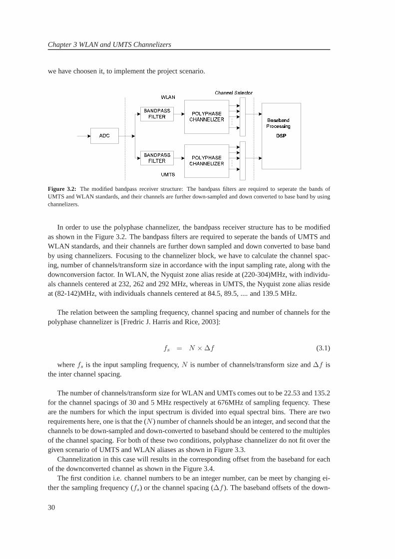
Figure 3.2: The modified bandpass receiver structure: The bandpass filters are required to seperate the bands ofUMTS and WLAN standards, and their channels are further down-sampled and down converted to base band by usingchannelizers.
In order to use the polyphase channelizer, the bandpass receiver structure has to be modifiedas shown in the Figure 3.2. The bandpass filters are required to seperate the bands of UMTS andWLAN standards, and their channels are further down sampledand down converted to base bandby using channelizers. Focusing to the channelizer block, we have to calculate the channel spac-ing, number of channels/transform size in accordance with the input sampling rate, along with thedownconversion factor. In WLAN, the Nyquist zone alias reside at (220-304)MHz, with individu-als channels centered at 232, 262 and 292 MHz, whereas in UMTS, the Nyquist zone alias resideat (82-142)MHz, with individuals channels centered at 84.5, 89.5, .... and 139.5 MHz.
The relation between the sampling frequency, channel spacing and number of channels for thepolyphase channelizer is [Fredric J. Harris and Rice, 2003]:
fs = N × ∆f (3.1)
wherefs is the input sampling frequency,N is number of channels/transform size and∆f isthe inter channel spacing.
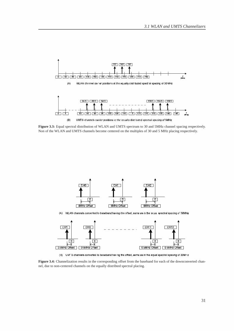
The number of channels/transform size for WLAN and UMTs comes out to be 22.53 and 135.2for the channel spacings of 30 and 5 MHz respectively at 676MHz of sampling fequency. Theseare the numbers for which the input spectrum is divided into equal spectral bins. There are tworequirements here, one is that the (N ) number of channels should be an integer, and second that thechannels to be down-sampled and down-converted to basebandshould be centered to the multiplesof the channel spacing. For both of these two conditions, polyphase channelizer do not fit over thegiven scenario of UMTS and WLAN aliases as shown in Figure 3.3.
Channelization in this case will results in the corresponding offset from the baseband for eachof the downconverted channel as shown in the Figure 3.4.
The first condition i.e. channel numbers to be an integer number, can be meet by changing ei-ther the sampling frequency (fs) or the channel spacing (∆f ). The baseband offsets of the down-
30
3.1 WLAN and UMTS Channelizers
! " # $ % & ' $ & % " ! $ $ ## ! !# # # !& (# % # % # & #& $ ! (#$ & (# % ! (#% & (# ! (#
)* + ,-.)*+ , -./ 0 12 3
Figure 3.3: Equal spectral distribution of WLAN and UMTS spectrum to 30 and 5MHz channel spacing respectively.Non of the WLAN and UMTS channels become centered on the multiples of 30 and 5 MHz placing respectively.
4 5 6 67 8 5 9 : ; ; < = > 4 5 ? 67 8 5 9 : ; ; < = > 4 5 @ 67 8 5 9 : ; ; < = >4 5 ? 66 AB 8 5 9 : ; ; < = > 4 5 @ 66 AB 8 5 9 : ; ; < = > 4 5 ? ? 66 AB 8 5 9 : ; ; < = > 4 5 ? @ 66 AB 8 5 9 : ; ; < = >CD E F G D H I J K L L = M< I N L O = P > = Q > N R K < = R K L Q J K O S L T > J = N ; ; < = > U < K V = K < S L > J = = W X K M < Y = I > P K M < Y K I S L T N ; Z 6 8 5 9C [ E \ 8 ] ^ I J K L L = M< I N L O = P > = Q > N R K < = R K L Q J K O S L T > J = N ; ; < = > U < K V = K < S L > J = = W X K M < Y = I > P K M < Y K I SL T N ; Z 6 8 5 9
Figure 3.4: Channelization results in the corresponding offset from the baseband for each of the downconverted chan-nel, due to non-centered channels on the equally distribtedspectral placing.
31

Chapter 3 WLAN and UMTS Channelizers
converted channels due to voilation of the second requiremnt, can be treated by having follwingthree ways:
• One is to change the sampling frequency and chosen such that the aliases of UMTS andWLAN channels satisfy the required demands of being at the equal spectral intervals.Different sampling frequencies instead of 676MHz are tried(frequencies lower than 676MHz),keeping the required aliases of UMTS and WLAN non-overlapped, in order to meet the in-teger number of channels and equal spectral spacing, but nonof them satisfied both of theseconditions.
• Second way is to use the channelizer as it is, with unequal channel placements but havingthe first condition true. In order to compensate the resultedfrequency offset from the baseband, the signal can be further hyterodyned and lowpass filtered, as shown in the Figure 3.5.
! " ##$ % &' ( ) * ! " ##$ % &' ( )
+ , ' ) - , . % . /Figure 3.5: Frequency offset from the base band is compensated by further hyterodyned and lowpass filteringthe signal.
But this is not an efficient structure, since it uses an extra filter and a mixer for each of thechannel, resulting in the requirement of more hardware resources. The required mixer cansimply be restricted to±1 or 0, if the required hytrodyne is a simple translation from thequarter sampling rate to the base band, thus avoiding the useof actual multiplication.
• The third way is to made some changes in the polyphase structure so that this hetrodyninggets embedded in it. Now a variant of the polyphase structurehaving the required funtion-ality is described [Harris, 2006]. The Z-transform of the frequency translated version of theprototype filter impluse response is:
H(Z) =
N−1∑
n=0
h(n)ej(2π/M)nkZ−n (3.2)
and the 1-to-M polyphase partition of it is:
H(Z) =
M−1∑
r=0
(N/M)−1∑
n=0
h(r + nM)ej(2π/M)(r+nM)kZ−(r+nM) (3.3)
=M−1∑
r=0
ej(2π/M)rkZ−r
(N/M)−1∑
n=0
h(r + nM)ej(2π/M)nMkZ−nM (3.4)
32
3.1 WLAN and UMTS Channelizers
When the frequency index k is an integer.2πnk is congruent to2π, and the selected fre-quency bin, bin k, aliases to zero in the polyphase partition. A variant of this relation shipis obtained by replacingk with k + s/d, where s= 0,1,2...d-1. Lets taked = 4 and thesbecomes 0,1,2,3. and the resulted equation is:
H(Z) =
M−1∑
r=0
ej(2π/M)r(k+s/4)Z−r
(N/M)−1∑
n=0
h(r + nM)ej(2π/M)nM(k+s/4)Z−nM(3.5)
=M−1∑
r=0
ej(2π/M)r(k+s/4)Z−r
(N/M)−1∑
n=0
h(r + nM)ej(2π/4)nsZ−nM (3.6)
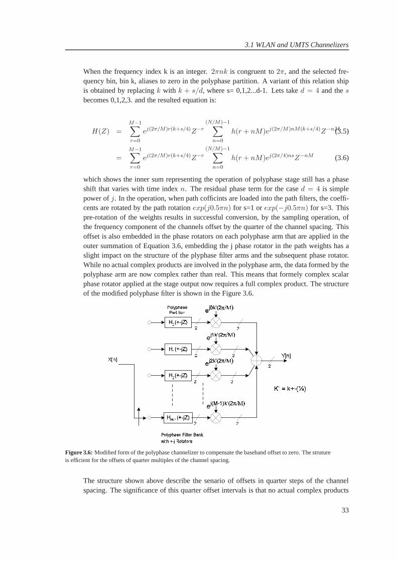
which shows the inner sum representing the operation of polyphase stage still has a phaseshift that varies with time indexn. The residual phase term for the cased = 4 is simplepower ofj. In the operation, when path cofficints are loaded into the path filters, the coeffi-cents are rotated by the path rotationexp(j0.5πn) for s=1 orexp(−j0.5πn) for s=3. Thispre-rotation of the weights results in successful conversion, by the sampling operation, ofthe frequency component of the channels offset by the quarter of the channel spacing. Thisoffset is also embedded in the phase rotators on each polyphase arm that are applied in theouter summation of Equation 3.6, embedding the j phase rotator in the path weights has aslight impact on the structure of the plyphase filter arms andthe subsequent phase rotator.While no actual complex products are involved in the polyphase arm, the data formed by thepolyphase arm are now complex rather than real. This means that formely complex scalarphase rotator applied at the stage output now requires a fullcomplex product. The structureof the modified polyphase filter is shown in the Figure 3.6. ! "
# $ % & ' ( ) * + , -
....... .. / 0 12 3 45 6
7 8 9 : ; 8 9 :Figure 3.6: Modified form of the polyphase channelizer to compensate thebaseband offset to zero. The strutureis efficient for the offsets of quarter multiples of the channel spacing.
The structure shown above describe the senario of offsets inquarter steps of the channelspacing. The significance of this quarter offset intervals is that no actual complex products
33
Chapter 3 WLAN and UMTS Channelizers
are involved in the polyphase arms. The offsets other than the quarter one can be achievedin the polyphase structure but doing so results in complex products in the polyphase arms,requiring more hardware resources.
3.1.1 Conclusions
The methods for compensating the offsets of the downconverted signals to baseband havebeen discussed above and it is seen that the modified polyphase structure is more efficient.Furthermore the modified structure is best for the offsets ofquarter multiples of the channelsspacing.
3.2 Modified System Design
Based on the conclusions above, it is seen that the offset of the quarters of the channel spac-ing can be efficiently downconverted to the baseband. But even this modification does not helpin transforming the UMTS and WLAN channels to baseband, because in WLAN the offsets of8MHz is not the quarter sub-multiple of channel spacing of 30MHz and in UMTS the offsets of0.5MHz is not the quarter sub-multiple of channel spacing of5MHz. In order to fit the polyphasechannelizers, there can be two options:
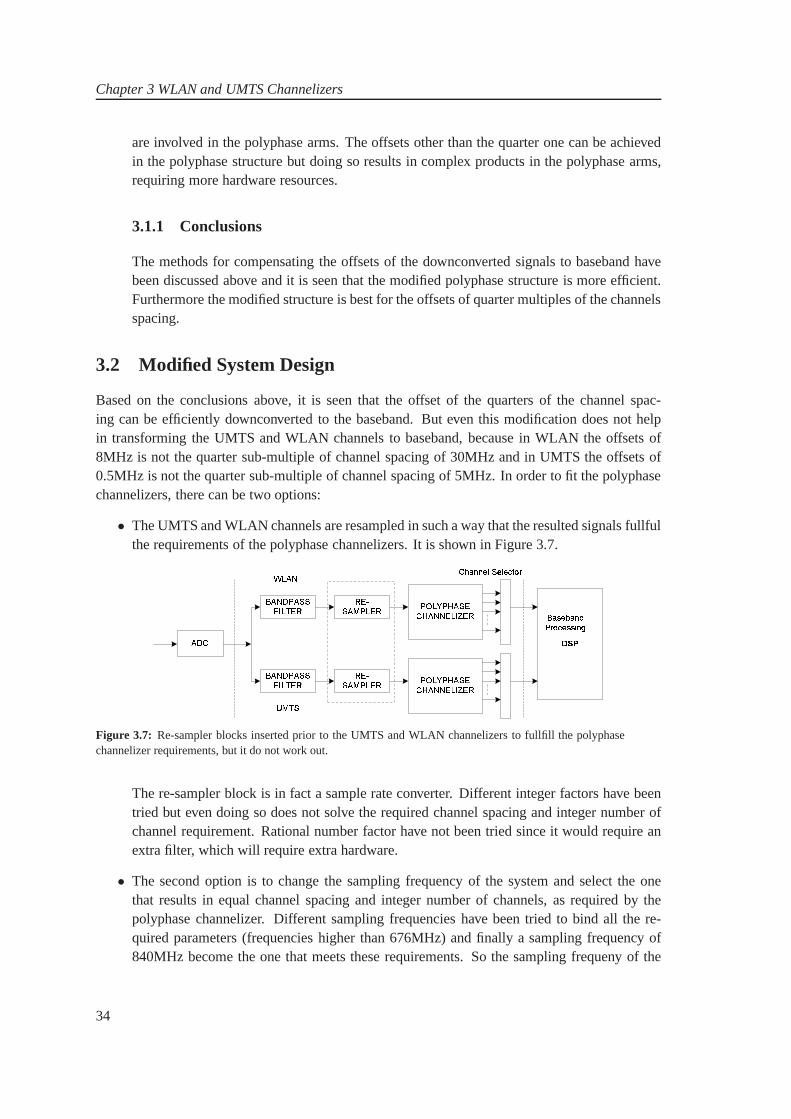
• The UMTS and WLAN channels are resampled in such a way that theresulted signals fullfulthe requirements of the polyphase channelizers. It is shownin Figure 3.7.
! "
# $ % $ % $
Figure 3.7: Re-sampler blocks inserted prior to the UMTS and WLAN channelizers to fullfill the polyphasechannelizer requirements, but it do not work out.
The re-sampler block is in fact a sample rate converter. Different integer factors have beentried but even doing so does not solve the required channel spacing and integer number ofchannel requirement. Rational number factor have not been tried since it would require anextra filter, which will require extra hardware.
• The second option is to change the sampling frequency of the system and select the onethat results in equal channel spacing and integer number of channels, as required by thepolyphase channelizer. Different sampling frequencies have been tried to bind all the re-quired parameters (frequencies higher than 676MHz) and finally a sampling frequency of840MHz become the one that meets these requirements. So the sampling frequeny of the
34

3.2 Modified System Design
! " # ! $ % & ' ( ) * + , - + . /0 , -+ 1 2 0 /3 -4 5 3 * + , * 6, 5 7 8 9 : ; < = > ( ? @ -5 0 + , A 65 * 2 B /A , C D E 9 F G* + , 3 H A ? I J 0 -5 3 K 6 A J 0 A + . I ) * + , 7 4 E L 9 F G @ . M + 3 * -+ 5 3 H A * / -* 5 A 5 M K 3 H A 5 3 * + , * 6, 5 -1 + * /5 N : H A * / -* 5 A 5 M K3 H A . M 2 ) -+ A , ) * + , M K O P E 9 F G * 6 A + M + 4 M Q A 6 /* B B A , N : H A = > ( ? * + , 8 9 : ; ) M 3 H * 6 A 5 B A . 3 6 * / /I - + Q A 63 A , -+3 H A ? J 0 -5 3 K 6 A J 0 + . I G M + A N R S T U V W X YX Z [\ ] ^ _R S T U X Z [\ ] ^ _V W X YY ` a b [] cd e^ a b ^ f g `h i f ^Figure 3.8: The combined spectrum of UMTS and WLAN is bandpass sampled at840MHz, and the resultedaliases in the Nyquist zone are spectrally inverted.
system has been changed to 840MHz. The corrsponding sampling aliases are shown inFigure 3.8.
The corresponding channels of UMTS and WLAN are shown in Figure 3.9.
j k lj m lj n l j o l p l lj q l p rls t uvw x yz| ~ ~ | | | ~ | | | | ~ | ~| | | | ~ ¡ ~| | | | ¢ |
p l q l n l m l rl lo lk l r rl r£ ll Figure 3.9: Individual channels: (12 UMTS channels and 3 WLAN channels). Each of UMTS channel is 5MHzwide and have 5MHz of spacing between inter-channel carriers, whereas each of the WLAN channel is 24MHzwide and have 30MHz of spacing between inter-channel carriers.
The channel spacing for UMTS is set to be 5MHz that corresponds to 168 channels for theinput frequency of 840MHz, whereas for WLAN, channel spacing is set to be 24MHz thatcorresponds to 35 channels. The channel positions of UMTS and WLAN on the spectraldistribution of 5MHz and 24MHz are shown in Figure 3.9.
It is seen from the Figure 3.9 that in the case of UMTS, all the channels centered at theoffset of half of the channel spacing (2nd multiple of the quarter of channel spacing), so thecorresponding value ofs becomes 2 and channel numberk varies from 70 to 81. So onepolyphase structure can extract all the channels at the sametime. In the case of WLAN,the arrangement is somehow different. Channels are centered at positions characterized by(k=2,s=0),(k=3,s=1),(k=4,s=2). This means that for each of the channel, one has to changethes parameter. This will limit the extraction of WLAN channel toone at a time, and de-pends on the value ofs along with value ofk. Since we deal with only one of the channelsfrom UMTS and WLAN at a time, so it does not make a difference. The channel spacingand corresponding number of channels are listed in Table 3.1.
35

Chapter 3 WLAN and UMTS Channelizers
! " # $ %% ! $ % & ' % & ' '' & # % & # ' & ! % & ! ' & % & '% & # (' % %& " '& " % % ' % $%& ' ! ('& ' (' % ! (' % ('& " ! ('
)* + , - .)* + , - ./ 0 1 2 3
$ $# 4 5 $4 5 4 5 &4 5 $4 5 4 5 &4 5 $%4 5 $ $4 5 $ 6 7 8 9 : 8 % ; 6 7 8 & 9 : 8 $ ; 6 7 8 9 : 8 ;
6 7 8 ! % 9 : 8 ; 6 7 8 $ 9 : 8 ;Figure 3.10: Equal spectral distribution of WLAN and UMTS spectrum to 30 and 5MHz channel spacingrespectively. UMTS channels become centered on the multiples of 5MHz plus two quarters of 5MHz, whereasin WLAN channels, one become centered on the multiples of 24MHz, another requires an extra offset of onequarter of 24MHz and the other requires an extra offset of twoquarters of 24MHz.
Specifications for UMTS and WLAN channelizersCases Sampling rate Channel Spacing No. of Channels
(MHz) (MHz)UMTS 840 5 168WLAN 840 24 35
Table 3.1: Specifications for the channelizer for UMTS and WLAN
36
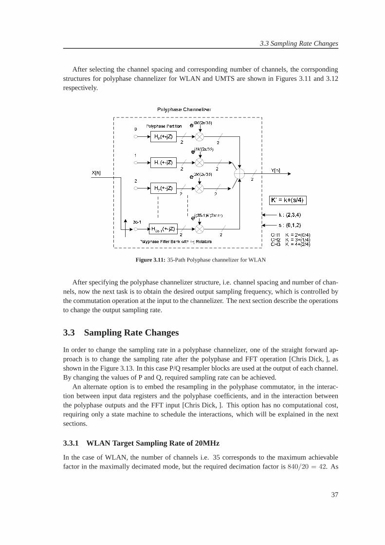
3.3 Sampling Rate Changes
After selecting the channel spacing and corresponding number of channels, the corrspondingstructures for polyphase channelizer for WLAN and UMTS are shown in Figures 3.11 and 3.12respectively. ! " ! # $ % &
! ' ( ) " * + ! , - . / 0 1 2 3 4 5
6 7 8 9 ) :
; < = > ? < = >@ A B C D E F G H I J K L M@ A G C D E F N H I B K L M@ A N C D E F L H IG K L M
"' ( ) "
O P QR S T U V W X T U Y Y W Q Z[ W \
] ^ _ `a `b V ^ c ` d `_ Figure 3.11: 35-Path Polyphase channelizer for WLAN
After specifying the polyphase channelizer structure, i.e. channel spacing and number of chan-nels, now the next task is to obtain the desired output sampling frequency, which is controlled bythe commutation operation at the input to the channelizer. The next section describe the operationsto change the output sampling rate.
3.3 Sampling Rate Changes
In order to change the sampling rate in a polyphase channelizer, one of the straight forward ap-proach is to change the sampling rate after the polyphase andFFT operation [Chris Dick, ], asshown in the Figure 3.13. In this case P/Q resampler blocks are used at the output of each channel.By changing the values of P and Q, required sampling rate can be achieved.
An alternate option is to embed the resampling in the polyphase commutator, in the interac-tion between input data registers and the polyphase coefficients, and in the interaction betweenthe polyphase outputs and the FFT input [Chris Dick, ]. This option has no computational cost,requiring only a state machine to schedule the interactions, which will be explained in the nextsections.
3.3.1 WLAN Target Sampling Rate of 20MHz
In the case of WLAN, the number of channels i.e. 35 corresponds to the maximum achievablefactor in the maximally decimated mode, but the required decimation factor is840/20 = 42. As
37

Chapter 3 WLAN and UMTS Channelizers
! " # ! " $ % & ' ! " # ( ) * # + , ! " - . / 0 1 2 3 4 5 6
7 8 9 : * ; < = > ? @ = > ?
A B C D E F G H I J K L MN OA B L D E F G H C J K L MN OA B CL D E F G P C J K L MN O
## ( ) * #
Q R ST U V W X Y Z V W [ [ Y S \] Y ^_ ` a b ca d e f fg d X ` h
Figure 3.12: 168-Path Polyphase channelizer for UMTS
i j k l mn n mo p qr s t u v wo u xy z y zp | u ~ s qw u y u i
k j j k j j k j j k j j k j j
Figure 3.13: Straight forward approach is to change the sampling rate after the polyphase and FFT opera-tion [Chris Dick, ]. In this case P/Q resampler blocks are used at the output of each channel. By changing the values ofP and Q, required sampling rate can be achieved.
38

3.3 Sampling Rate Changes
mentioned eariler, that any arbitrary sampling rate can be achieved by simply modifying the com-mutation operation.
The task is to modify the input commutator to support the 42-to-1 down sample rather than thestandard 35-to-1 down sample. This is an almost trivial task. The modified resampling is arrangedby keeping the 35-path filter, but feeding 42 ports from the commutator. The commutator for thestandard 35-point polyphase filter starts at port 34 and delivers 35 successive inputs to ports 34,33, 32, and so on through 0, the modified commutator starts at port 6 and delivers 7 successiveinputs to ports 6, 5, 4, and so on through 0, and again startingfrom the bottom i.e. 34, 33 and so onthrough 0 thus completing 42 inputs. The previous data at theport is shifted before accomodataingnext data. Input memory for the 35-path filter must be modifiedto support this long commutatorinput schedule. The mapping structure of the reindexing scheme is best seen in the original one-dimensional prototype filter shown in figure and then transferred to the two-dimensional polyphasepartition [Harris, 2006].
Figure 3.14: Memory contents for successive 42-point input data blocks into a 35-point prototype pre-polyphasepartitioned filter and FFT. !"#$#%"!&!'"!!!("(%( "'
)"( !"#$#%"!&!'"!!!("(%( "')"(' ")'))")()*"$ $#"%)%$"%*
&" #Figure 3.15: Memory contents for successive 42-point input data blocks into a 35-point polyphase filter.
39
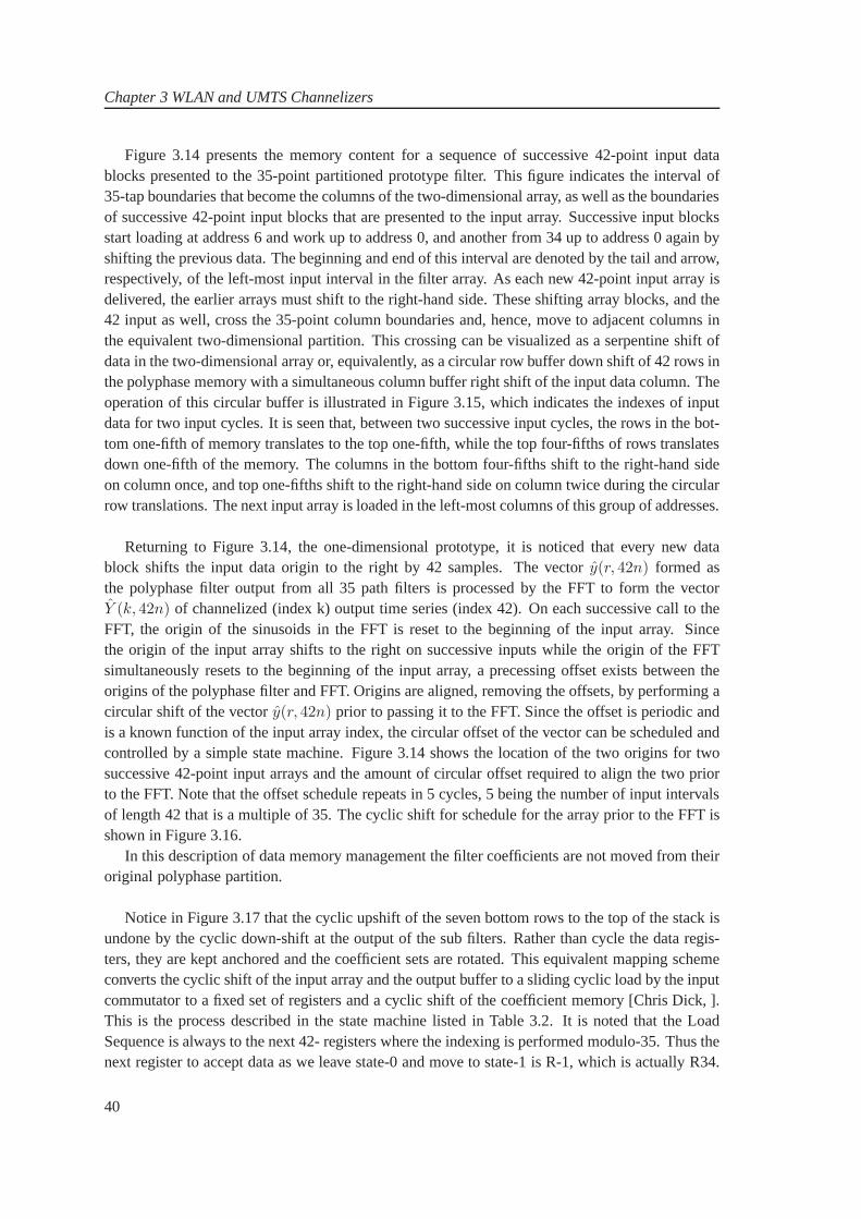
Chapter 3 WLAN and UMTS Channelizers
Figure 3.14 presents the memory content for a sequence of successive 42-point input datablocks presented to the 35-point partitioned prototype filter. This figure indicates the interval of35-tap boundaries that become the columns of the two-dimensional array, as well as the boundariesof successive 42-point input blocks that are presented to the input array. Successive input blocksstart loading at address 6 and work up to address 0, and another from 34 up to address 0 again byshifting the previous data. The beginning and end of this interval are denoted by the tail and arrow,respectively, of the left-most input interval in the filter array. As each new 42-point input array isdelivered, the earlier arrays must shift to the right-hand side. These shifting array blocks, and the42 input as well, cross the 35-point column boundaries and, hence, move to adjacent columns inthe equivalent two-dimensional partition. This crossing can be visualized as a serpentine shift ofdata in the two-dimensional array or, equivalently, as a circular row buffer down shift of 42 rows inthe polyphase memory with a simultaneous column buffer right shift of the input data column. Theoperation of this circular buffer is illustrated in Figure 3.15, which indicates the indexes of inputdata for two input cycles. It is seen that, between two successive input cycles, the rows in the bot-tom one-fifth of memory translates to the top one-fifth, whilethe top four-fifths of rows translatesdown one-fifth of the memory. The columns in the bottom four-fifths shift to the right-hand sideon column once, and top one-fifths shift to the right-hand side on column twice during the circularrow translations. The next input array is loaded in the left-most columns of this group of addresses.
Returning to Figure 3.14, the one-dimensional prototype, it is noticed that every new datablock shifts the input data origin to the right by 42 samples.The vectory(r, 42n) formed asthe polyphase filter output from all 35 path filters is processed by the FFT to form the vectorY (k, 42n) of channelized (index k) output time series (index 42). On each successive call to theFFT, the origin of the sinusoids in the FFT is reset to the beginning of the input array. Sincethe origin of the input array shifts to the right on successive inputs while the origin of the FFTsimultaneously resets to the beginning of the input array, aprecessing offset exists between theorigins of the polyphase filter and FFT. Origins are aligned,removing the offsets, by performing acircular shift of the vectory(r, 42n) prior to passing it to the FFT. Since the offset is periodic andis a known function of the input array index, the circular offset of the vector can be scheduled andcontrolled by a simple state machine. Figure 3.14 shows the location of the two origins for twosuccessive 42-point input arrays and the amount of circularoffset required to align the two priorto the FFT. Note that the offset schedule repeats in 5 cycles,5 being the number of input intervalsof length 42 that is a multiple of 35. The cyclic shift for schedule for the array prior to the FFT isshown in Figure 3.16.
In this description of data memory management the filter coefficients are not moved from theiroriginal polyphase partition.
Notice in Figure 3.17 that the cyclic upshift of the seven bottom rows to the top of the stack isundone by the cyclic down-shift at the output of the sub filters. Rather than cycle the data regis-ters, they are kept anchored and the coefficient sets are rotated. This equivalent mapping schemeconverts the cyclic shift of the input array and the output buffer to a sliding cyclic load by the inputcommutator to a fixed set of registers and a cyclic shift of thecoefficient memory [Chris Dick, ].This is the process described in the state machine listed in Table 3.2. It is noted that the LoadSequence is always to the next 42- registers where the indexing is performed modulo-35. Thus thenext register to accept data as we leave state-0 and move to state-1 is R-1, which is actually R34.
40
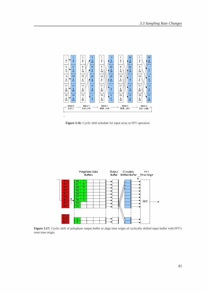
3.3 Sampling Rate Changes
Figure 3.16: Cyclic shift schedule for input array to FFT operation.
! " # $% & ' $ ($) *++& ,% - .,/ * $ , !0 # .++& 1 ) *++ & ,2 *(" *() *++ & ,
3 343 344 .5 & 2 , .6 .7
Figure 3.17: Cyclic shift of polyphase output buffer to align time originof cyclically shifted input buffer with FFT’sreset time origin.
41

Chapter 3 WLAN and UMTS Channelizers
In a similar fashion the filter weights assigned to perform the inner products with the registers arealways offset -7 modulo 35 relative to the previous filter set.
State Machines for LOAD and FILTER coefficientsSTATE LOAD FILTERS
0 R6, R5 ,...,R0,R34,R33,...,R0 C0, C1 ,.................,C341 R34,R33,...,R0,R34,R33,...,R28C7, C6 ,...,C34,C0,C1,...,C62 R27,R26,...,R0,R34,R33,...,R21C14,C13,...,C34,C0,C1,...,C133 R20,R19,...,R0,R34,R33,...,R14C21,C22,...,C34,C0,C1,...,C204 R13,R12,...,R0,R34,R33,...,R7 C28,C29,...,C34,C0,C1,...,C27
Table 3.2: State Machines for register loads and filter coefficients
3.3.2 UMTS Target Sampling Rate of 61.44MHz
In the case of UMTS, the number of channels i.e. 168 corresponds to the maximum achievablefactor in the maximally decimated mode, but the required decimation factor is840/61.44 = 13.67.
The required resampling ratio the process is then 13.6 or 68/5. This ratio can be realized byfirst up sampling the input stream by 5 and then down sampling by 68. The up sampling is per-formed by zero packing the input data and the down sampling byserpentine shifting data throughthe filter in stride of length 68. This process is illustratedfor two data load iterations in Figure 3.18.
Figure 3.18: Successive serpentine data shifts in polyphase memory and data load for a 68/5 re-sampling in a 168-stagepolyphase filter. It shows just two data load operations.
There is no actual zero packing in the final configuration, This is just to illustrate, how the(non-zero) data memory interacts with coefficient memory. It is worth noting that in the first dataload, the left Figure, 14-actual data samples are deliveredto the 68 register addresses, while in thesecond load 13-actual data samples are delivered to the 68 register addresses. The data loadingprocedure is found to be periodic in 210-load cycles for which it will require 210-states to controlthe process. (The least common multiple of 68 and 168 is 2856,and since 68 zeropacked inputs
42

3.3 Sampling Rate Changes
are delivered at a time, results in 42 states. For upsamplingfactor of 5, the LCM of 42 and 5becomes 210, which is the periodic interval). Table 3.3 lists the memory loading instructions forthe process that anchors the data registers and cycles the data load and coefficient sets. Note that inthe 210-states, a total of 2856 inputs are delivered and takefrom the polyphase engine 210 outputsto realize the desired embedded 68/5 resampling. The loading scheme is seen to be a constantoffset of -5 modulo 168 within a sequence as well as in the transition between sequences. The -5offset is a consequence of the 1-to-5 up sampling represented by the zero packing but not actuallyimplemented in the process.
State Machines for LOAD SequenceSTATE No. of Inputs LOADING SEQUENCE
0 14 R67, R62, R57, R52, R47, R42, R37, R32, R27, R22, R17, R12, R7,R21 13 R165, R160, R155, R150, R145, R140, R135, R130, R125, R120, R115, R110, R1052 14 R100, R95, R90, R85, R80, R75, R70, R65, R60, R55, R50, R45, R40, R35| | || | || | |
208 13 R34, R29, R24, R19, R14, R9, R4, R167, R162, R157, R152, R147,R142209 14 R137, R132, R127, R122, R117, R112, R107, R102, R97, R92, R87, R82, R77, R72
Table 3.3: Polyphase filter’s Data loading sequence with the state machine
Because of the 1-to-5 up sampling implemented by the zero packing, only one fifth of theweights in each stage actually contributes to the subfilter output. Thus each stage is further par-titioned into 5 sub sets of weights, which results in a total of 168 × 5 = 840 filter weight sets.These sets are denoted by C0, C1,..., C839 where the integer is the starting index from the originalnon-partitioned prototype filter. Each filter starts with its index and increments in stride of length840. Table 3.4 lists the filter assignment to the 168-successive data registers for 210-states of theprocess.
Table 3.4 shows that in a given state the successive filter index increments by 169 modulo-840and between states, the filter index increments by 68 modulo-840. The integer 169 is the offsetbetween two data samples in the zero-packed load in two adjacent rows. The 68 index is the num-ber of zero-packed data points introduced per data load cycle.
State Machines for FILTER Co-efficientsSTATE FILTER Co-efficients sets
0 C0, C169, C338, C507, C676,................,C836, C165, C334, C5031 C68, C237, C406, C575, C744,...............,C64, C223,C402, 571| || || |
209 C772, C101, C270, C439, C608,..............,C599, C768, C97, C266, C435
Table 3.4: Filter Co-efficients loading sequence with the state machine
43

Chapter 3 WLAN and UMTS Channelizers
In the design process of up sample the data by a factor of five onthe way into the filter requiresthat the prototype filter has to be designed to operate at 5 timesfs or 4200 MHz. Consequently,the filter becomes five times longer than the standard design but since only one-fifth of it is usedper processing cycle so no processing penalty is paid.
The 1-to-5 zero-packed signal presents 5 spectral copies tothe processing stream of filter andFFT. Figure 3.19 indicates the frequency indices of the spectra prior to up sampling and afterthe 1-to-5 up sampling. By examining the spectra of the up sampled data at the frequencies thatcorrespond to the pre-up sampled locations, i.e. multiplesof 2π/168, different spectral centersare obsevered. For instance, the spectra at2π/168 at the input rate is frequency "1", but at theoutput rate there is frequency "5". The spectral locations are re-ordered as a result of processingthe up-sampled data in the polyphase filter. This re-ordering is an expected result and is seen in theGood-Thomas (or Prime Factor) algorithm as the result of reside addressing of a-two dimensionalarray [Chris Dick, ]. Thus the FFT processing the polyphase data outputs frequencies in the order[0, 5, 10, 15, .....,158,163,168], which is seen to be indexing stride of 5 modulo-168. The responseto the observed rearranged indices is to re-order them back to their natural order.
Figure 3.19: Re-ordering of the spectral locations as a result of processing the up-sampled data in the polyphase filter
3.4 Observations
In the polyphase channelizer for WLAN, which has 35 channelsof 24 MHz at the input samplingrate of 840 MHz and UMTS, which has 168 channels of 5MHz at the input sampling frequency of840MHz, there are some observations which are:
• In UMTS, the filter designed for polyphase channelizer has tooperate on 5 times the inputsampling frequency of 840MHz, results in a very long-lengthfilter. The filter is decomposedto have 840 sets of 168 sub-filter coefficients. Although onlyone-fifth of the cofficients areused at a time, but it requires large memory to store all the filter coefficients.
• There are total of 168 channels, from which the desired are only 12 of them and only one isused at a time.
44

3.4 Observations
• Similarly in WLAN, there are total of 35 channels, but the desired are 3 of them and onlyone is used at a time.
This puts the extra load on the filtering process in terms of high clock speed requirement andlarge memory storage for filter coefficients.
In order to lower down these burdens, one of the ways is to decrease the sampling frequency ofthe signal, that can be done by resampling the signal before the polyphase channelizer input. Theidea is that the sampling frequency should be kept as low as possible (not to have overlap aliases).The resampling factor should be chosen such that the resampled signal for WLAN and UMTShave integer number of channels of 5MHz and 30 MHz (or 24MHz asin previous case) respec-tively based on the new sampling frequency. The second thingis that the correponding aliasedchannels of WLAN and UMTS must be centered on their channel placing or on the multiples ofthe quarter of their channel spacing respectively.
Based on the above criteria, different resampling factors for WLAN and UMTS have beentried, which are listed in Tables 3.5 and 3.6.
WLAN Resampling processDownsampling New Sampling Freq. Channel Status Channelfactor (MHz) Integer/non-Integer
2 420 non-overlapped non-integer3 280 non-overlapped non-integer4 210 overlapped non-integer5 168 overlapped integer6 140 overlapped non-integer
Table 3.5: Resampling factors for WLAN, showing the channel status as overlapped/non-overlapped and resultingnumber of channels as integer/non-integer.
UMTS Resampling processDownsampling New Sampling Freq. Channel Status Channelfactor (MHz) Integer/non-Integer
4 210 non-overlapped integer5 168 non-overlapped non-integer6 140 overlapped integer7 120 overlapped integer8 105 overlapped integer
Table 3.6: Resampling factors for UMTS, showing the channel status as overlapped/non-overlapped and resultingnumber of channels as integer/non-integer.
It is seen from the Table 3.5 that non of the resampling factors satisfy the two mentioned con-ditions. Similarly Table 3.6 shows that only one resamplingfactor i.e. 4 satisfy the two abovementioned conditions.
The bottleneck in the resampling process is the image signalthat do not allow the resamplingby large factors. This restriction can be omitted if the bandpass filters for WLAN and UMTS
45
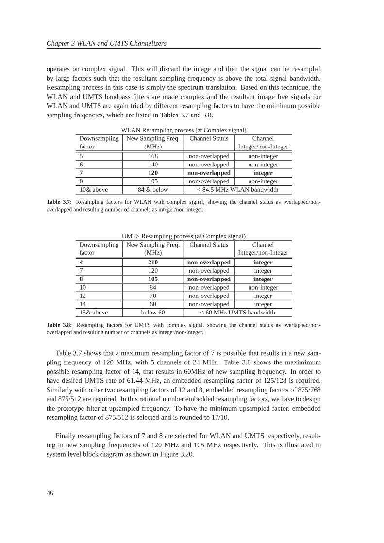
Chapter 3 WLAN and UMTS Channelizers
operates on complex signal. This will discard the image and then the signal can be resampledby large factors such that the resultant sampling frequencyis above the total signal bandwidth.Resampling process in this case is simply the spectrum translation. Based on this technique, theWLAN and UMTS bandpass filters are made complex and the resultant image free signals forWLAN and UMTS are again tried by different resampling factors to have the mimimum possiblesampling freqencies, which are listed in Tables 3.7 and 3.8.
WLAN Resampling process (at Complex signal)Downsampling New Sampling Freq. Channel Status Channelfactor (MHz) Integer/non-Integer
5 168 non-overlapped non-integer6 140 non-overlapped non-integer7 120 non-overlapped integer8 105 non-overlapped non-integer10& above 84 & below < 84.5 MHz WLAN bandwidth
Table 3.7: Resampling factors for WLAN with complex signal, showing the channel status as overlapped/non-overlapped and resulting number of channels as integer/non-integer.
UMTS Resampling process (at Complex signal)Downsampling New Sampling Freq. Channel Status Channelfactor (MHz) Integer/non-Integer
4 210 non-overlapped integer7 120 non-overlapped integer8 105 non-overlapped integer10 84 non-overlapped non-integer12 70 non-overlapped integer14 60 non-overlapped integer15& above below 60 < 60 MHz UMTS bandwidth
Table 3.8: Resampling factors for UMTS with complex signal, showing the channel status as overlapped/non-overlapped and resulting number of channels as integer/non-integer.
Table 3.7 shows that a maximum resampling factor of 7 is possible that results in a new sam-pling frequency of 120 MHz, with 5 channels of 24 MHz. Table 3.8 shows the maximimumpossible resampling factor of 14, that results in 60MHz of new sampling frequency. In order tohave desired UMTS rate of 61.44 MHz, an embedded resampling factor of 125/128 is required.Similarly with other two resampling factors of 12 and 8, embedded resampling factors of 875/768and 875/512 are required. In this rational number embedded resampling factors, we have to designthe prototype filter at upsampled frequency. To have the minimum upsampled factor, embeddedresampling factor of 875/512 is selected and is rounded to 17/10.
Finally re-sampling factors of 7 and 8 are selected for WLAN and UMTS respectively, result-ing in new sampling frequencies of 120 MHz and 105 MHz respectively. This is illustrated insystem level block diagram as shown in Figure 3.20.
46

3.4 Observations
! "#$ %&
' ( ( !) $ %&
* + * + , ( " #- ./ 0 %12 , " 3 4+ 56 78 99: * 8; < ; = + > 7? @ * 98: = + >7? A : *; 9: = + > + B C+ B < 9:A + >98: + > D) D ) )E F 0 %12 D) D ) ) E G H I/ / %12Figure 3.20: Modified system block diagram having re-samplers prior to UMTS and WLAN channelizers.
Based on the above results, a re-sampling factor of 7 is selected for WLAN and the samplingfrequency is reduced to 105MHz. The corresponding band of WLAN channels translate to (-42,-12 and 48)MHz. Based on the change in the input sampling frequency, the polyphase channelizerhas to be restructured. The modified channelizer for WALN is shown in Figure 3.21 with reducednumbers of polyphase sub-filters.J K LM N O P Q R J P ST UT U K VW X YZ [\ ] ^W _ YZ [\ ] ^ ` a b c d ef g h i j` a k c d ef g h i jW l YZ [\ ] ^W m n _ YZ [\ ] ^
` a f c d ef g h i j` a eo p k q c ref g h i j s t u v w xy z |ffff
fff ffJ K LM N O P Q R U L T R S ~ P V c UT O pa K T P T K SQ
bkfo p k ¡¢ £ Y¤ ¥¦ § ^
¨ © Yª «¬ « ^ © Y® «¯ «ª ^Figure 3.21: Modified WLAN channelizer.
With the sampling frequency of 120MHz and channel spacing of24MHz, the number of chan-nels become 5 which is the number of the polyphase decomposition. Now the new downfactor tohave 20MHz required rate at 120MHz sampling frequency, is 6.This is realized by down samplingby serpentine shifting data through the filter in stride of length 6. This overall process is same asin the previous case with sampling frequency of 840MHz. The only difference is the shifting datathrough the filter of 5 stages in stride of length 6, instead ofshifting data through the filter of 35stages in stride of length 42. The modified process is illustrated for two data load iterations inFigure 3.22.
A resampling factor of 8 is selected for UMTS and the samplingfrequency is reduced to105MHz. The corresponding band of UMTS channels translate to (35.5 to -12.25)MHz. Basedon the change in the input sampling frequency, the polyphasechannelizer has to be restructured.
47

Chapter 3 WLAN and UMTS Channelizers
Figure 3.22: Successive serpentine data shifts in polyphase memory and data load for 6:1 re-sampling in a 5-stagepolyphase filter. It shows just two data load operations.
The modified channelizer for UMTS is shown in Figure 3.23 withreduced numbers of polyphasesub-filters. ! "# $ % & ' ( & )* +* + ! ,- . /0 12 3 4- 5 /0 12 3 4 6 7 8 9 : ;< = > ? @A6 7 B 9 : ;< = > ? @A- C /0 12 3 4- C 5 D 5 /0 12 3 4
6 7 < 9 : ;< = > ? @A6 7 ;< B E B F 9 G ;< = > ? @A H I J K L MN OP Q<<<<
<<< << ! "# $ % & ' ( R + " * ( ) S & , 9 T +* % U E7 V ! * & * ! )'
W X Y Z [ X Y Z8B<< B E B
\ ] ^_ ` a b c d e a b f f d ^gh d ij kc k l
Figure 3.23: Modified UMTS cahnnelizer
With the sampling frequency of 105MHz and channel spacing of5MHz, the number of chan-nels become 21 which is the number of the polyphase decomposition. Now the new downfactorto have 61.44MHz required rate at 105MHz sampling frequency, is 1.7 or 17/10. This ratio canbe realized by first up sampling the input stream by 10 and thendown sampling it by 17. The upsampling is performed by zero packing the input data and the down sampling by serpentine shift-ing data through the filter in stride of length 17. This overall process is same as in the previouscase with sampling frequency of 840MHz. The only differenceis the shifting data through thefilter of 21 stages in stride of length 17, instead of shiftingdata through the filter of 168 stagesin stride of length 68. The modified process is illustrated for two data load iterations in Figure 3.24.
There is no actual zero packing in the final configuration. In the first data load, the Figure 3.24a,2-actual data samples are delivered to the 17 register addresses, while in the second load 2-actualdata samples are delivered to the 17 register addresses. Thedata loading procedure is found to beperiodic in 210-load cycles for which it will require 210-states to control the process. (The leastcommon multiple of 21 and 17 is 357, and since 17 zeropacked inputs are delivered at a time,results in 21 states. For upsampling factor of 10, the LCM of 21 and 10 becomes 210, whichis the periodic interval). The periodic factor is same as in the previous case. Table 3.9 lists the
48
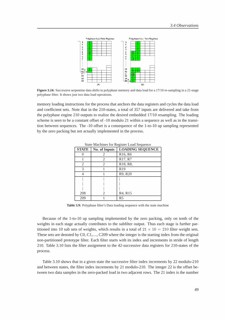
3.4 Observations
Figure 3.24: Successive serpentine data shifts in polyphase memory and data load for a 17/10 re-sampling in a 21-stagepolyphase filter. It shows just two data load operations.
memory loading instructions for the process that anchors the data registers and cycles the data loadand coefficient sets. Note that in the 210-states, a total of 357 inputs are delivered and take fromthe polyphase engine 210 outputs to realize the desired embedded 17/10 resampling. The loadingscheme is seen to be a constant offset of -10 modulo 21 within asequence as well as in the transi-tion between sequences. The -10 offset is a consequence of the 1-to-10 up sampling representedby the zero packing but not actually implemented in the process.
State Machines for Register Load SequenceSTATE No. of Inputs LOADING SEQUENCE
0 2 R16, R61 2 R17, R72 2 R18, R8,3 1 R194 1 R9, R20| | || | || | |
208 2 R4, R15209 1 R5
Table 3.9: Polyphase filter’s Data loading sequence with the state machine
Because of the 1-to-10 up sampling implemented by the zero packing, only on tenth of theweights in each stage actually contributes to the subfilter output. Thus each stage is further par-titioned into 10 sub sets of weights, which results in a totalof 21 × 10 = 210 filter weight sets.These sets are denoted by C0, C1,...., C209 where the integeris the starting index from the originalnon-partitioned prototype filter. Each filter starts with its index and increments in stride of length210. Table 3.10 lists the filter assignment to the 42-successive data registers for 210-states of theprocess.
Table 3.10 shows that in a given state the successive filter index increments by 22 modulo-210and between states, the filter index increments by 21 modulo-210. The integer 22 is the offset be-tween two data samples in the zero-packed load in two adjacent rows. The 21 index is the number
49
Chapter 3 WLAN and UMTS Channelizers
of zero-packed data points introduced per data load cycle.
State Machines for FILTER Co-efficientsSTATE FILTER Co-efficients sets
0 C0, C22, C44, C66, C88,................,C164, C186, C208,C201 C17, C39, C61, C83, C105,...............,C181, C203, C15,C372 C34, C56, C78, C100, C122,...............,C198, C10, C32,C54| || || |
209 C193, C5, C27, C49, C71,..............,C147, C169, C191, C3
Table 3.10:Filter Co-efficients loading sequence with the state machine
The prototype filter has to be designed to operate at 10 timesfs or 1050 MHz due to up samplethe data by a factor of ten on the way into the filter. Consequently, the filter becomes ten timeslonger than the standard design but since only one-tenth of it is used per processing cycle so noprocessing penalty is paid.
50

CHAPTER 4
SIMULATIONS
A filter is essentially a system or a network that selectivelychange the wave shape in the formof magnitude-frequency and phase-frequency characteristics of the signal. A digitial filter is a setof mathematical equations which forms an algorithm and thatcan be implemented in hardware orsoftware to produce a desired output against the specific input [Emmanuel C. Ifeachor, 2002]. Thenature of modification of the signal is dependent on the phaseand amplitude characteristics of thefilter. Some useful definitions are explained below, which will guide us to better understanding ofthe filters design flow.
Phase/Group Delay.The phase delay or group delay provides a useful measure of how the filtermodifies the phase characteristics of the signal. Phase delay is the amount of delay that eachfrequency component of the composite signal suffers, as it passes through the filter. Thegroup delay on the other hand is anaveragetime delay the composite signal suffers at eachfrequency. Mathematically the phase delay i.e.Tp is the negative of the phase angle dividedby frequency, whereas the group delay i.e.Tg is the negative of the derivitive of the phasewith respect to frequency:
Tp = −θ(w)/w (4.1)
Tg = −dθ(w)/dw (4.2)
A filter with non-linear phase characteristics (i.e the delay not proportional with frequency)causes the phase distortion in the signal that passes through it.
Symmetric Impulse Response.A filter is said to have linear phase response if its phase responsesatisfies one of the following condition.
θ(w) = −αw (4.3)
θ(w) = β − αw (4.4)
51

Chapter 4 Simulations
whereα andβ are constant. If a filter satisfies the equation 4.3 it will have both constantphase/group delay response and it must have positive symmetry, and is described mathemat-ically as:
h(n) = h(N − n − 1)
n = 0, 1, . . . , (N − 1)/2 (N : Odd)
n = 0, 1, . . . , (N/2) − 1 (N : Even)(4.5)
(4.6)
α = (N − 1)/2 (4.7)
Whereas, if the equation 4.4 of linear phase of the filter is satisfied then it will have onlyconstant group delay. In this case the impulse response havenegative or anti symmetry,which is expressed as:
h(n) = −h(N − n − 1) (4.8)
α = (N − 1)/2 (4.9)
β = pi/2 (4.10)
4.1 Digital Filter
There are two classes of digital filters i.e. finite impulse response (FIR) and an infinite impulseresponse (IIR) filter. The question of economics also arise in implementation of digital filter. Theeconomic concerns are mainly measure interms of hardware complexity, chip area, and computa-tional speed, If we put aside the linear consideration in IIRfilters then it can be the best choice, butsince many application does require least phase distortionin passband and also the fact that FIRfilters have been supported by special purpose DSP which havemultiplier and accumulator thathelp to reduce the computational speed of higher order FIR filters. The FIR filters have mainlybeen analyzed for algorithmic devolopment and for simulations due to the reason that the channelsof the WLAN and UMTS are compactly placed in the spectrum and the phase distortion in thepassband can cause severe interference.
4.1.1 FIR Filters
The brief summary of the methods for finding the FIR filter coefficients is explined below. Gener-ally there are three methods for finding the FIR filter coefficients
1. Window Method
2. Optimal Method
3. Frequency Selective Method
The most common choice among the methods for finding the FIR filter coefficients is awindowmethod. The flow of this method for calculating the filter coefficients is:
52

4.1 Digital Filter
• Specify the desired frequency responsse of the filterHd(w).
• Obtain the impulse responsehd(n) of the desired filter by taking the inverse Fourier trans-form. This impulse response tends towards the infinity.
• To truncate the infinite impulse response, an appropriate window function that satisfies thepassband and stopband attenuation specifications, is multiplied with the desired impulseresponse to determine the number of filter coefficients.
The window method is a most common choice, as it requires the least computational require-ments, simple, and is easy to understand, but it has some limitations:
Lack Of Flexibility. Both the peaks of passband and stopband are equal, so the designer may endup with either too small passband ripples or too larger stopband attenuation. Therefore thedesigner does not have a freedom to select the parameters according to its requirement.
Approximation Issues. The window method does not provide individual control over the approx-imation error in different bands. The approximation of the desired frequency response havepeaks in the passband ripples near the band edges and decreases away from the band edges.
The better approximation of the desired frequency responsecan be achieved by evenly dis-tributed ripples in the passband or stopband that oscillates between1 + δp and 1 − δp, in thepassband and between0 to δs,in the stopband. whereδp andδs are the passband and the stopbandripples respectively. TheOptimal filter is the one which provides such an approximation withequal ripple design and is known asequiripple design. The above discussion is shown in Figure4.1.
! ! " "
# $ % &#'( )* )+ ', )- *.% &# '( )* )+ ', )-*.Figure 4.1: Comparision of the frequency response of a low pass filter(a)the window filter and (b) the optimal filter. In(a) the ripples are larger near the band edge; and in (b) the ripples have same peaks(equiripple) in passband or stopband
The difference between the ideal and practical response canbe viewed as error function:
E(w) = W (w)[Hd(w) − H(w)] (4.11)
where, w ǫ Ω
Hd(w) : desired response
53

Chapter 4 Simulations
H(w) : practical response
W (w) is a weighting function which provides the relative error control over the different bands,for the low pass filter. It is defined as:
W (w) =
1/K 0 ≤ w ≥ wp,
1 wp ≤ w ≥ pi,(4.12)
(4.13)
The objective in the optimal filter design is to determine thefilter coefficientsh(n) such thatthe value of the maximum weighted approximation error|E(w)| is minimized in the passbandand stopband, this particular criterion used in the design procedure of Park-MaClellan algorithmis calledminimaxor chebyshev[J. H. McClellan and Rabiner, 1973]. Mathematically it can beexpressed as:
‖E(w)‖ = min[max |E(w)|] (4.14)
The second issue of flexibility have been overcome in the optimal design by two approaches[?]. In the first approach, developed by Hermann and schusslerN, δp andδs parametrs are fixedandwp, ws are variables, whereas in the second procedure from Park MaClellan N,wp, ws andthe ratio ofδp/δs parametrs are fixed andδp, δs are variables. The algorithmic details for theseapproaches can be found from [J. H. McClellan and Rabiner, 1973].
4.1.2 Summary of Equiripple Optimal Filter
• choose the required design specifications i.e sampling frequency, band edge and transitionwidth (normalized form), passband ripples and stopband attenuation.
• Then calculate the order of the filter (there is different formula for the bandpass and low passfilter). The following formula calculates the order of the bandpass filter [Emmanuel C. Ifeachor, 2002].
N ≈D∞(δp, δs)
∆F− f(δp, δs)∆F + 1 (4.15)
∆F : is a normalized transition width.
D∞(δp, δs) = log(δs)[b1(log(δp))2 + b2(log(δp))+ b3] + [b4(log(δp))
2 + b5(log(δp))+ b6]
(4.16)
f(δp, δs) = −14.6 log(δp/δs) − 16.9 (4.17)
All the b’s coeffients are approximated and are listed in [Emmanuel C. Ifeachor, 2002].
• After finding the filter taps then the proper weights for the passband and stopband can befind by the ratio of passband to stopband ripples.
54
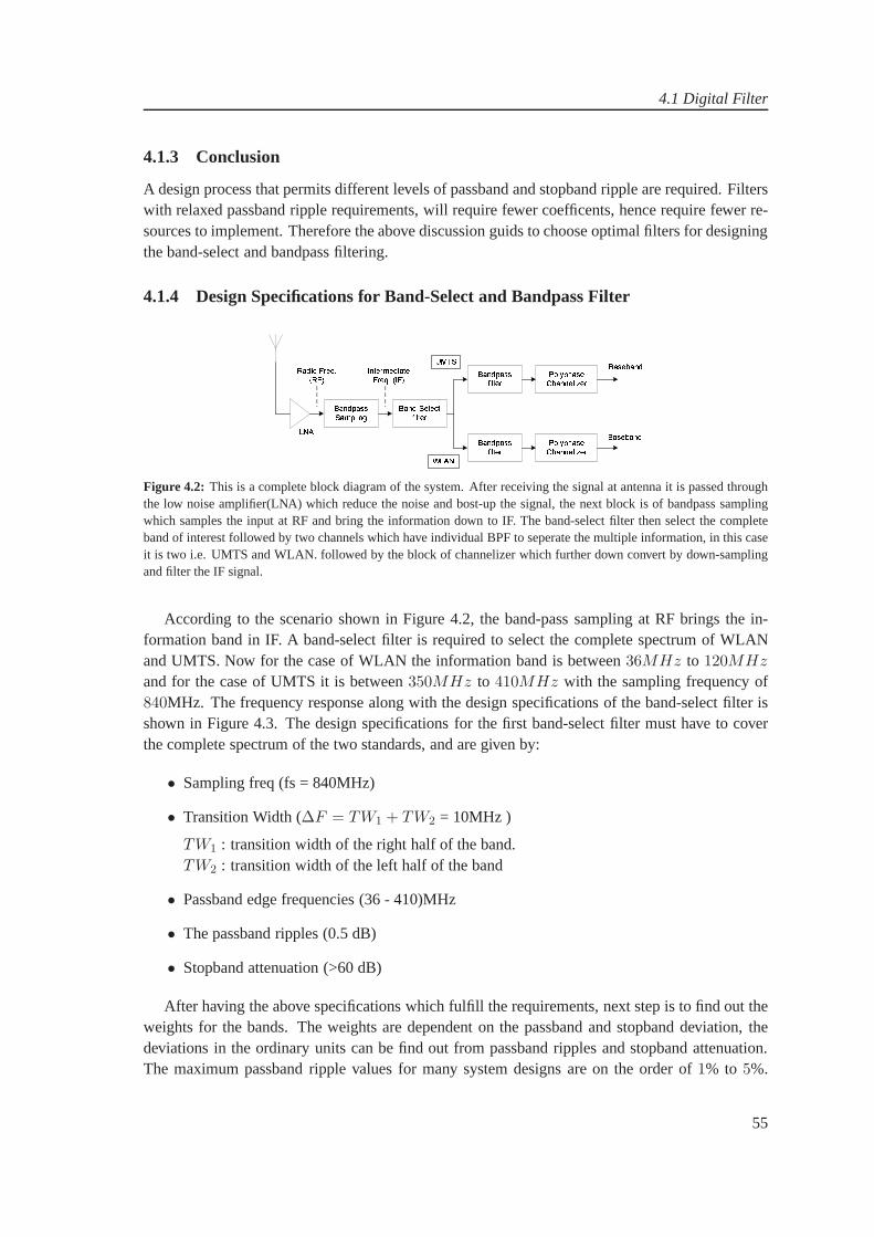
4.1 Digital Filter
4.1.3 Conclusion
A design process that permits different levels of passband and stopband ripple are required. Filterswith relaxed passband ripple requirements, will require fewer coefficents, hence require fewer re-sources to implement. Therefore the above discussion guidsto choose optimal filters for designingthe band-select and bandpass filtering.
4.1.4 Design Specifications for Band-Select and Bandpass Filter
! "#$%!
Figure 4.2: This is a complete block diagram of the system. After receiving the signal at antenna it is passed throughthe low noise amplifier(LNA) which reduce the noise and bost-up the signal, the next block is of bandpass samplingwhich samples the input at RF and bring the information down to IF. The band-select filter then select the completeband of interest followed by two channels which have individual BPF to seperate the multiple information, in this caseit is two i.e. UMTS and WLAN. followed by the block of channelizer which further down convert by down-samplingand filter the IF signal.
According to the scenario shown in Figure 4.2, the band-passsampling at RF brings the in-formation band in IF. A band-select filter is required to select the complete spectrum of WLANand UMTS. Now for the case of WLAN the information band is between36MHz to 120MHz
and for the case of UMTS it is between350MHz to 410MHz with the sampling frequency of840MHz. The frequency response along with the design specifications of the band-select filter isshown in Figure 4.3. The design specifications for the first band-select filter must have to coverthe complete spectrum of the two standards, and are given by:
• Sampling freq (fs = 840MHz)
• Transition Width (∆F = TW1 + TW2 = 10MHz )
TW1 : transition width of the right half of the band.TW2 : transition width of the left half of the band
• Passband edge frequencies (36 - 410)MHz
• The passband ripples (0.5 dB)
• Stopband attenuation (>60 dB)
After having the above specifications which fulfill the requirements, next step is to find out theweights for the bands. The weights are dependent on the passband and stopband deviation, thedeviations in the ordinary units can be find out from passbandripples and stopband attenuation.The maximum passband ripple values for many system designs are on the order of1% to 5%.
55
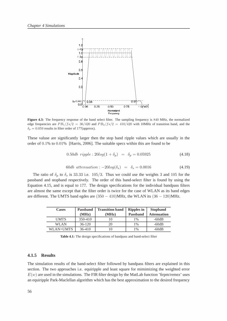
Chapter 4 Simulations
!"#$%& " '!(
)Figure 4.3: The frequency response of the band select filter. The sampling frequency is840 MHz, the normalizededge frequencies arePB1/fs/2 = 36/420 andPB2/fs/2 = 410/420 with 10MHz of transition band, and theδp = 0.059 results in filter order of 177(apprrox).
These valuse are significantly larger then the stop band ripple values which are usually in theorder of0.1% to0.01% [Harris, 2006]. The suitable specs within this are found tobe
0.50db ripple : 20log(1 + δp) = δp = 0.05925 (4.18)
60db attenuation : −20log(δs) = δs = 0.0016 (4.19)
The ratio ofδp to δs is 33.33 i.e. 105/3. Thus we could use the weights3 and105 for thepassband and stopband respectively. The order of this band-select filter is found by using theEquation 4.15, and is equal to177. The design specifications for the individual bandpass filtersare almost the same except that the filter order is twice for the case of WLAN as its band edgesare different. The UMTS band egdes are(350 − 410)MHz, the WLAN its (36 − 120)MHz.
Cases Passband Transition band Ripples in Stopband(MHz) (MHz) Passband Attenuation
UMTS 350-410 10 1% -60dBWLAN 36-120 20 1% -60dB
WLAN+UMTS 36-410 10 1% -60dB
Table 4.1: The design specifications of bandpass and band-select filter
4.1.5 Results
The simulation results of the band-select filter followed bybandpass filters are explained in thissection. The two approaches i.e. equiripple and least square for mimimizing the weighted errorE(w) are used in the simulations. The FIR filter design by the MatLab function ’firpm/remez’ usesan equiripple Park-Maclellan algorithm which has the best approximation to the desired frequency
56

4.1 Digital Filter
response in the minimax sense. However, it may not be desirable if we want to minimize the energyof the error signal, Concequently if we want to reduce the energy of the error signalE(w) as muchas possible in certain frequency bands, least square designis preferrable. The MatLab function’firls’ provides a measure that minimizes the error in the least square sense that is 2-norm i.e.(‖E(w)‖2).
0 0.2 0.4 0.6 0.8 1−15000
−10000
−5000
0
5000
Normalized Frequency (Hz)
Pha
se (
degr
ees)
Phase Response
0 0.2 0.4 0.6 0.8 1−100
−50
0
50
Normalized Frequency (Hz)
Mag
nitu
de (
dB)
Magnitude Response of ’firls’
Figure 4.4: The magnitude and phase response of the ’firls’. The ripples in the passband and in the stopband areminimum in the magnitude response, with the constant group delay in the passband.
The simulation results of the band-select filter with both equiripple and with the least squaredesign are carried out. The Figure 4.4 shows the phase and themagnitude response of the filterwith ’firls’. The ripples in the passband and in the stopband are minimum which is visible fromthe magnitude response in Figure 4.6 and the stopband attenuation is around50dB on the average.The phase reponse has a constant group delay meaning that every frequency component is facingthe same delay. The result from the ’firpm/remez’ equirippledesign is very much similar exceptthe fact that there are equal ripple in the pass/stop band in the magnitude response as shown inFigure 4.6. These ripples are not minimize to zero as it is in the case of ’firls’. The stop bandattenuation is much better for the case of equiripple designwith the same specs i.e order,transitionwidth.
The impulse response for both the functions are shown in Figures 4.7 and 4.8. The filter co-efficients obtained from the function ’firls’ have anOdd Symmetryash(n) = −h(N − n − 1),whereas the function ’firpm’ have anEven Symmetrywith h(n) = h(N − n − 1). So the linearphase characteristics of these FIR filters help to reduce thecomputation by exploiting this sym-metry. Therefore the effective order of the FIR filter isN/2, which means that the computationalresourses would also be reduced by factor of2, and the overall computational speed would becomedouble.
The magnitude and phase response of the individual bandpassfilters that seperate the multiple-band are shown in the Figures 4.9 and 4.10. The least square algorithm provides the best fit as it
57
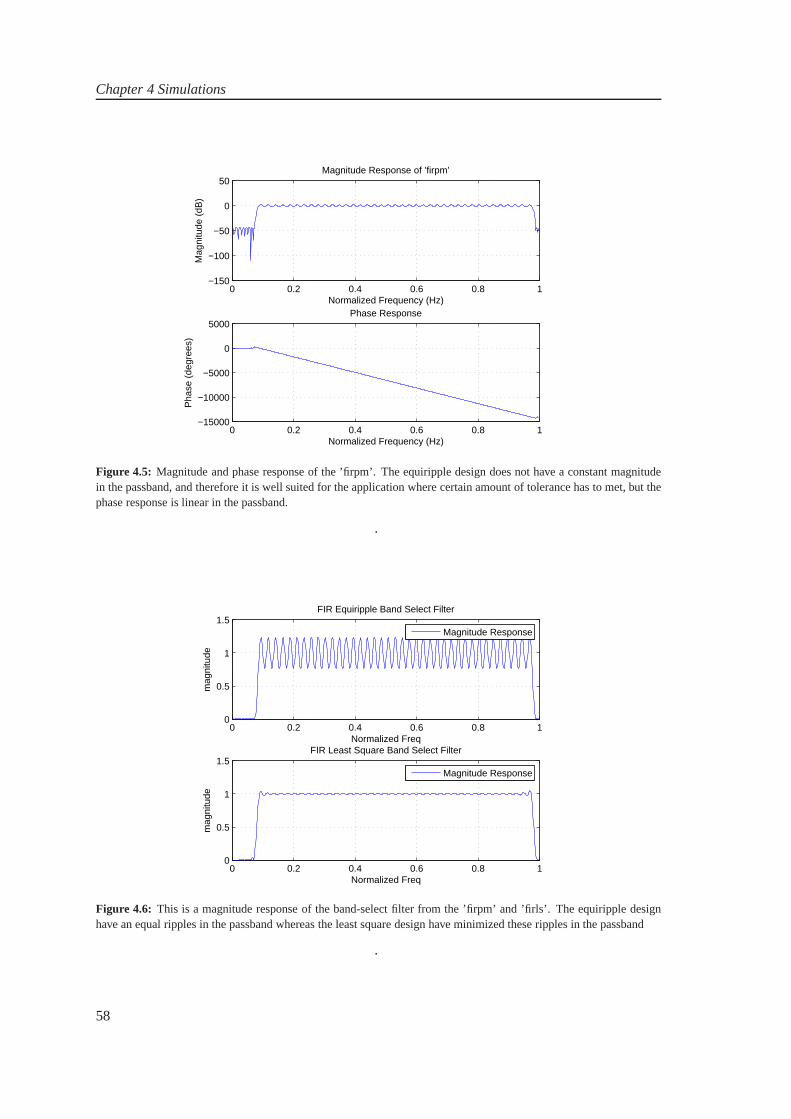
Chapter 4 Simulations
0 0.2 0.4 0.6 0.8 1−15000
−10000
−5000
0
5000
Normalized Frequency (Hz)
Pha
se (
degr
ees)
Phase Response
0 0.2 0.4 0.6 0.8 1−150
−100
−50
0
50
Normalized Frequency (Hz)
Mag
nitu
de (
dB)
Magnitude Response of ’firpm’
Figure 4.5: Magnitude and phase response of the ’firpm’. The equiripple design does not have a constant magnitudein the passband, and therefore it is well suited for the application where certain amount of tolerance has to met, but thephase response is linear in the passband.
.
0 0.2 0.4 0.6 0.8 10
0.5
1
1.5FIR Equiripple Band Select Filter
Normalized Freq
mag
nitu
de
Magnitude Response
0 0.2 0.4 0.6 0.8 10
0.5
1
1.5FIR Least Square Band Select Filter
Normalized Freq
mag
nitu
de
Magnitude Response
Figure 4.6: This is a magnitude response of the band-select filter from the ’firpm’ and ’firls’. The equiripple designhave an equal ripples in the passband whereas the least square design have minimized these ripples in the passband
.
58

4.1 Digital Filter
0 20 40 60 80 100 120 140 160 180−0.8
−0.6
−0.4
−0.2
0
0.2
0.4
0.6
0.8
Filter Taps
Mag
nitu
de
Impulse Response Of BSF(firls)
Figure 4.7: The impulse response of the band-select filter by ’firls’. It has an odd symmetry with half of the filtercoefficients are same i.e h(n) = -h(N-n-1)
0 20 40 60 80 100 120 140 160 180−0.3
−0.2
−0.1
0
0.1
0.2
0.3
0.4
0.5
0.6
Filter Taps
Mag
nitu
de
Impulse response of BSF (firpm)
Figure 4.8: The impulse response of the band-select filter by ’firpm’. It has an even symmetry with half of the filtercoefficients are same i.e h(n) = h(N-n-1).
.
59
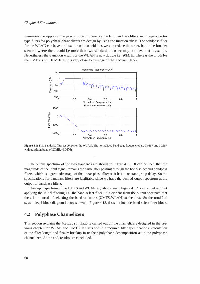
Chapter 4 Simulations
minimizes the ripples in the pass/stop band, therefore the FIR bandpass filters and lowpass proto-type filters for polyphase channelizers are design by using the function ’firls’. The bandpass filterfor the WLAN can have a relaxed transition width as we can reduce the order, but in the broaderscenario where there could be more than two standards then wemay not have that relaxation.Nevertheless the transition width for the WLAN is now doublei.e. 20MHz, whereas the width forthe UMTS is still 10MHz as it is very close to the edge of the stectrum (fs/2).
0 0.2 0.4 0.6 0.8 1−2000
−1000
0
1000
Normalized Frequency (Hz)
Pha
se (
degr
ees)
Phase Response(WLAN)
0 0.2 0.4 0.6 0.8 1−150
−100
−50
0
50
Normalized Frequency (Hz)
Mag
nitu
de (
dB)
Magnitude Response(WLAN)
Figure 4.9: FIR Bandpass filter response for the WLAN. The normalized band edge frequencies are 0.0857 and 0.2857with transition band of 20MHz(0.0476)
.
The output spectrum of the two standards are shown in Figure 4.11. It can be seen that themagnitude of the input signal remains the same after passingthrough the band-select and pandpassfilters, which is a great advantage of the linear phase filter as it has a constant group delay. So thespecifications for bandpass filters are justifiable since we have the desired output spectrum at theoutput of bandpass filters.
The ouput spectrum of the UMTS and WLAN signals shown in Figure 4.12 is an output withoutapplying the initial filtering i.e. the band-select filter. It is evident from the output spectrum thatthere isno needof selecting the band of interest(UMTS,WLAN) at the first. Sothe modifiedsystem level block diagram is now shown in Figure 4.13, does not include band-select filter block.
4.2 Polyphase Channelizers
This section explains the MatLab simulations carried out onthe channelizers designed in the pre-vious chapter for WLAN and UMTS. It starts with the required filter specifications, calculationof the filter length and finally breakup in to their polyphase decomposition as in the polyphasechannelizer. At the end, results are concluded.
60
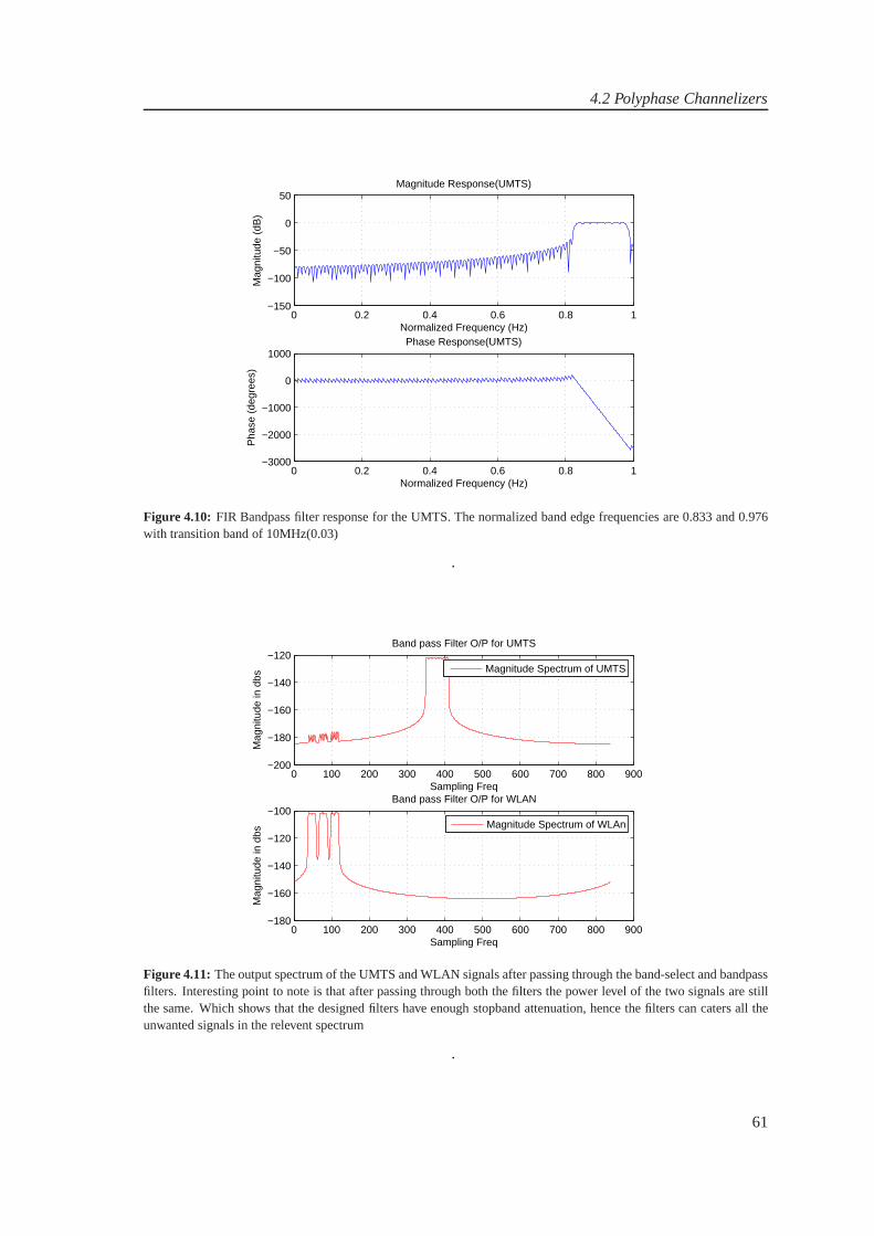
4.2 Polyphase Channelizers
0 0.2 0.4 0.6 0.8 1−3000
−2000
−1000
0
1000
Normalized Frequency (Hz)
Pha
se (
degr
ees)
Phase Response(UMTS)
0 0.2 0.4 0.6 0.8 1−150
−100
−50
0
50
Normalized Frequency (Hz)
Mag
nitu
de (
dB)
Magnitude Response(UMTS)
Figure 4.10: FIR Bandpass filter response for the UMTS. The normalized band edge frequencies are 0.833 and 0.976with transition band of 10MHz(0.03)
.
0 100 200 300 400 500 600 700 800 900−200
−180
−160
−140
−120Band pass Filter O/P for UMTS
Sampling Freq
Mag
nitu
de in
dbs
Magnitude Spectrum of UMTS
0 100 200 300 400 500 600 700 800 900−180
−160
−140
−120
−100Band pass Filter O/P for WLAN
Sampling Freq
Mag
nitu
de in
dbs
Magnitude Spectrum of WLAn
Figure 4.11: The output spectrum of the UMTS and WLAN signals after passing through the band-select and bandpassfilters. Interesting point to note is that after passing through both the filters the power level of the two signals are stillthe same. Which shows that the designed filters have enough stopband attenuation, hence the filters can caters all theunwanted signals in the relevent spectrum
.
61

Chapter 4 Simulations
0 100 200 300 400 500 600 700 800 900−200
−180
−160
−140
−120Band pass Filter O/P for UMTS
Sampling Freq
Mag
nitu
de in
dbs
Magnitude Spectrum of UMTS
0 100 200 300 400 500 600 700 800 900−180
−160
−140
−120
−100Band pass Filter O/P for WLAN
Sampling Freq
Mag
nitu
de in
dbs
Magnitude Spectrum of WLAn
Figure 4.12: The output spectrum of the UMTS and WLAN signals after passing through the band-select and bandpassfilters. Interesting point to note is that after passing through both the filters the power level of the two signals are stillthe same. Which shows that the designed filters have enough stopband attenuation, hence the filters can caters all theunwanted signals in the relevent spectrum
.
! !
" #$
%& "#$ ! ! Figure 4.13: The modified system level block diagram. The band-select filter is not required at the up-front for selectingthe band of information as the required performance can be achieved from the individual bandpass filters.
62

4.2 Polyphase Channelizers
4.2.1 Filter Specifications
In the previous chapter, it is discussed that the polyphase channelizer requires equal spectral distri-bution of the input sampling frequency to form channels. Theresulted channel spectral distributionfor UMTS and WLAN are 5MHz and 24MHz respectively. In polyphase channelizer, the filter isdesigned at the baseband. The corresponding desired filtersfor WLAN and UMTS are shown inFigures 4.14 and 4.15. In WLAN filter specifications, the passband bandwidth is 16.6MHz andthe transition bandwidth is 7.4MHz. The transition band is taken as the bandwidth between edgesof the passband of the adjacent channels. Similarly in the case of UMTS, the passband bandwidthis 3.84MHz and the transition bandwidth is 1.16MHz. The filter specifications are summarized inthe Table 4.2.
! "#$ %& ! "#$ %& ' ()* +,-. / 01.2 +3 +24- +567 35 / 89: ; <=466. ,+>./Figure 4.14: Filter specifications for WLAN channelizer. It has passbandbandwidth of 16.6MHz and the transitionbandwidth is 7.4MHz.
? @A @ B C D E F GABACADAEAFHIJ J KI LMKN OP QRS T UV
AGW XI LJ YZ Y[ L KI LM KN O \ Q\] T UV
^ _I L L` a b I cd YLefT UV^ _IL L` a b I cd YLefT UV g hT UVij klmn o p qn r ks krt m ku vw su o xy zp |t vvn lk n oFigure 4.15: Filter specifications for UMTS channelizer. It has passbandbandwidth of 3.84MHz and the transitionbandwidth is 1.16MHz.
Filter specification for UMTS and WLANCases PassBand Bandwidth Transition Bandwidth PassBand Stop band
(MHz) (MHz) Ripples AttenuationWLAN 16.6 7.4 1% -60dBUMTS 3.92 1.16 1% -60dB
Table 4.2: Filter specifications for UMTS and WLAN
63

Chapter 4 Simulations
In the design process of the filters, the first task is to determine the filter length. The designis based on equirripple optimal method. The filter length canbe approximated by the followingempirical formula [Harris, 2006]:
N ≈fs
∆f
Atten(dB)
22(4.20)
wherefs is the sampling frequency and∆f is the transition bandwidth. The MatLab expressionfor calculating the order of equiripple filter is:
FilterLength = firpmord(F,A,DEV,Fs) (4.21)
where′F ′ is a vector of cutoff frequencies in Hz, in ascending order between 0 and half thesampling frequency′F ′
s (Nyquist frequency).′A′ is a vector specifying the desired function’s am-plitude on the bands defined by′F ′. ′DEV ′ is a vector of maximum deviations or ripples (in linearunits) allowable for each band.
The next task is to calculate the filter coefficients for the calculated filter length and specifica-tions as given in the Table 4.2. MatLab functionfirls is used for calculating filter coefficients
B = firls(N,F,A) (4.22)
which returns a length N+1 linear phase (real, symmetric coefficients) FIR filter which has thebest approximation to the desired frequency response described by F and A in the least squaresense. F is a vector of frequency band edges in pairs, in ascending order between 0 and 1. 1corresponds to the Nyquist frequency or half the sampling frequency. A is a real vector the samesize as F which specifies the desired amplitude of the frequency response of the resultant filter B.
By using the MatLab expression, the corresponding filter length for WLAN comes out 41. Forpolyphase decomposition as in the case of polyphase channelizer for WLAN, the number of chan-nels is 5, which is also polyphase decomposition number. In order to have a integer number ofco-efficients in each of the decomposed sub-filters, the order is increased to 50, which correspondsto 10 coefficients in each of 5 sub-filters. The impluse response and frequency response of the pro-totype filter is shown in Figure 4.16.
The composite complex signal consisting of three WLAN channels is generated by adding theexponentials together, is not the original WLAN signal thathas been used in the bandpass filter-ing. The reason is that we need to have all of the WLAN channelsand in the original signal wehave only one of them. The purpose is to illustrate the functionality of Polyphase channelizer withmultiple channels. This is also the case for composite complex signal consisting of the twelveUMTS channels. The generated complex signal consisting of the three WLAN channels shown inFigure 4.17. It shows three channels centered at frequencies of -42, -12 and 48 MHz occupyinga bandwidth of 16.6MHz (useful bandwidth). The spectral placing is same as it would be in theoriginal WLAN signal.
The composite signal is fed to the polyphase channelizer forWLAN, along with the parame-ters of channel numberk and channel offsets to extract the desired channel. The channel centered
64
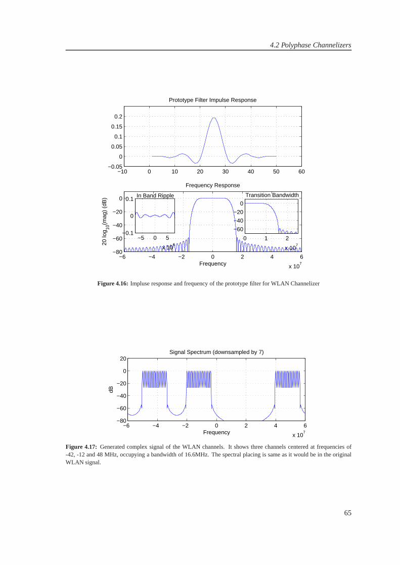
4.2 Polyphase Channelizers
−10 0 10 20 30 40 50 60−0.05
0
0.05
0.1
0.15
0.2
Prototype Filter Impulse Response
−6 −4 −2 0 2 4 6
x 107
−80
−60
−40
−20
0
Frequency Response
Frequency
20 lo
g 10(m
ag)
(dB
)
−5 0 5
x 106
−0.1
0
0.1In Band Ripple
0 1 2
x 107
−60
−40
−20
0
Transition Bandwidth
Figure 4.16: Impluse response and frequency of the prototype filter for WLAN Channelizer
−6 −4 −2 0 2 4 6
x 107
−80
−60
−40
−20
0
20Signal Spectrum (downsampled by 7)
Frequency
dB
Figure 4.17: Generated complex signal of the WLAN channels. It shows three channels centered at frequencies of-42, -12 and 48 MHz, occupying a bandwidth of 16.6MHz. The spectral placing is same as it would be in the originalWLAN signal.
65

Chapter 4 Simulations
at 48MHz corresponds to k=2, and s=0, and its output which is downconverted to baseband anddownsampled to the required sampling rate of 20MHz is shown in Figure 4.21.
−1 −0.8 −0.6 −0.4 −0.2 0 0.2 0.4 0.6 0.8 1
x 107
−80
−70
−60
−50
−40
−30
−20
−10
0Output Signal Spectrum @ 20MHz
dB
Figure 4.18: The channel centered at 48MHz corresponds to k=2, and s=0, isdownconverted to baseband and down-sampled to the required sampling rate of 20MHz.
In the polyphase channelizer for UMTS, a downsampling factor of 17/10 is required, which isachieved by simultaneously upsampling by 10 and downsampling by 17 in the polyphase commu-tator. This upsampling of factor 10 creates 10 copies of the signal. Thus, the filter as shown inFigure 4.15 has to be designed on the new sampling frequency,which is10× 105 = 1050MHz.
The corresponding filter length at frequency 1050MHz comes out 2301. For polyphase decom-position as in the case of polyphase channelizer for UMTS, the number of channels is 21, whichis also the polyphase decomposition number. In order to havea integer number of co-efficients ineach of the decomposed sub-filters, the order is increased to2520, which corresponds to 12 coef-ficients in each of 21 sub-filters. The impluse response and frequency response of the prototypefilter is shown in Figure 4.19.
The generated composite signal consisting of the UMTS channels and the signal downsam-pled by factor 8, is shown in Figure 4.20. It shows 12 channelscentered at frequencies of(15,20,25....70)MHz occupying a bandwidth of 3.84MHz. Thespectral placing is same as it wouldbe in the original UMTS signal.
The composite signal is fed to the polyphase channelizer forUMTS, along with the parametersof channel numberk and channel offsets to extract the desired channel. The channel centered at35 MHz corresponding to k=7 and s=2, is downconverted to baseband and downsampled to therequired sampling rate of 61.77MHz (61.44MHz) as shown in figure 4.21.
4.3 Conclusion
The composite complex signal consisting of three WLAN channels is generated by adding theexponentials together, is not the original WLAN signal thathas been used in the bandpass filtering.The reason is that we need to have all of the WLAN channels and in the original signal we have
66

4.3 Conclusion
0 500 1000 1500 2000−1
0
1
2
3
4
5x 10
−3 Prototype Filter Impulse Response (UMTS)
−2 −1 0 1 2 3
x 107
−80
−60
−40
−20
0
Frequency Response
Frequency
20 lo
g 10(m
ag)
(dB
)
−2 0 2
x 106
−0.2
0
0.2In Band Ripple
0 5
x 106
−60
−40
−20
0Transition Bandwidth
Figure 4.19: Impluse response and frequency of the prototype filter for UMTS Channelizer
−4 −3 −2 −1 0 1 2 3 4
x 108
−80
−60
−40
−20
0
20Input Signal Spectrum
Frequency
dB
−5 0 5
x 107
−80
−60
−40
−20
0
20Signal Spectrum (downsampled by 8)
Frequency
dB
Figure 4.20: Generated composite signal of the UMTS channels (Top Figure). The bottom figure shows the compositesignal downsamped by factor 8. 12 channels are translated tocenter frequencies of (15,20,25....70)MHz occupying abandwidth of 3.84MHz. The spectral placing is same as it would be in the original UMTS signal.
67

Chapter 4 Simulations
−3 −2 −1 0 1 2 3
x 107
−80
−60
−40
−20
0Output signal Spectrum CH−1
Frequency
dB
Figure 4.21: The channel centered at 35 MHz corresponding to k=7 and s=2, is downconverted to base band anddownsampled to the required sampling rate of 61.77MHz (61.44MHz).
only one of them. The purpose is to illustrate the functionality of Polyphase channelizer withmultiple channels. This is also the case for composite complex signal consisting of the twelveUMTS channels.
The prototype filter for WLAN has 50 taps which are partitioned into 5 polyphase sub-filters,so that each sub-filter has 10 coefficients, whereas the prototype filter for UMTS has 2520 tapswhich are partitioned into 210 polyphase sub-filters, so that each sub-filter has 12 coefficients.Only one tenth of the sub-filters i.e. 21 out of 210 are used at atime. This saves the processingpanelty due to embedded upsampling process. The recovered signals at the baseband has 50dB ofdynamic range.
68
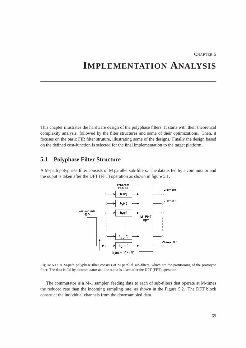
CHAPTER 5
I MPLEMENTATION ANALYSIS
This chapter illustrates the hardware design of the polyphase filters. It starts with their theoreticalcomplexity analysis, followed by the filter structures and some of their optimizations. Then, itfocuses on the basic FIR filter struture, illustrating some of the designs. Finally the design basedon the defined cost-function is selected for the final implementation to the target platform.
5.1 Polyphase Filter Structure
A M-path polyphase filter consists of M parallel sub-filters.The data is fed by a commutator andthe ouput is taken after the DFT (FFT) operation as shown in figure 5.1.
! " #
$ %$ &$ ' ( &
Figure 5.1: A M-path polyphase filter consists of M parallel sub-filters,which are the partitioning of the prototypefilter. The data is fed by a commutator and the ouput is taken after the DFT (FFT) operation.
The commutator is a M-1 sampler, feeding data to each of sub-filters that operate at M-timesthe reduced rate than the incoming sampling rate, as shown inthe Figure 5.2. The DFT blockconstruct the individual channels from the downsampled data.
69
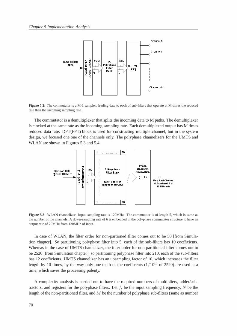
Chapter 5 Implementation Analysis
! " # $ $ %" # $ $ &" # $ $ ' ( &
)*++,-.-*/01234.-56 7 8 '9 7 8 '9Figure 5.2: The commutator is a M-1 sampler, feeding data to each of sub-filters that operate at M-times the reducedrate than the incoming sampling rate.
The commutator is a demultiplexer that splits the incoming data to M paths. The demultiplexeris clocked at the same rate as the incoming sampling rate. Each demultiplexed output has M timesreduced data rate. DFT(FFT) block is used for constructing multiple channel, but in the systemdesign, we focused one one of the channels only. The polyphase channelizers for the UMTS andWLAN are shown in Figures 5.3 and 5.4.
: ; ; < => ? @ A BC D E ? F ?G H I J K L M N O P Q C R S T UC D V W ? X X C B? F Y ? Z C [ ? X D \ ? FL M N O P U ? F C]_abcdebfghi_jekclm n Z o pq qr s t u vw x y z I | v~ z z y I H v~ v ~ y u H K M s~ z x I t y z I u y ~ z ~ u
Figure 5.3: WLAN channelizer: Input sampling rate is 120MHz. The commutator is of length 5, which is same asthe number of the channels. A down-sampling rate of 6 is embedded in the polyphase commutator structure to have anoutput rate of 20MHz from 120MHz of input.
In case of WLAN, the filter order for non-partioned filter comes out to be 50 [from Simula-tion chapter]. So partitioning polyphase filter into 5, eachof the sub-filters has 10 coefficients.Whereas in the case of UMTS channelizer, the filter order for non-partitioned filter comes out tobe 2520 [from Simulation chapter], so partitioning polyphase filter into 210, each of the sub-filtershas 12 coefficients. UMTS channelizer has an upsampling factor of 10, which increases the filterlength by 10 times, by the way only one tenth of the coefficents(1/10th of 2520) are used at atime, which saves the processing palenty.
A complexity analysis is carried out to have the required numbers of multipliers, adder/sub-tractors, and registers for the polyphase filters. Letfs be the input sampling frequency,N be thelength of the non-partitioned filter, andM be the number of polyphase sub-filters (same as number
70

5.2 Symmetric Structure
!" # $ % & '( ) * + , - . / " 0 1 2 3 " # 4 5 6 6 " ! % 7 ( " 8 6 # 9 %: ;< < , - . 3 % "=>?@ABCDEB>F>GHI?JIEKCLM ' ( N O PQ R Q RP P OS S S S TP P OS S S S T
U V W W Figure 5.4: UMTS channelizer: Input sampling rate is 105MHz. The commutator is of length 21, which is same as thenumber of the channels. A sampling-conversion rate of 17/10is embedded in the polyphase commutator structure tohave an output rate of 61.44MHz from 105MHz of input.
of channels), then the length of each sub-filter becomesN/M . For WLAN channelizer, each ofthe sub-filters of length (N/M ) 10-tapes require (N/M ) 10 multipliers, ((N/M)−1) 9 adders and((L/M)− 1) 9 registers that results in overall requirement of(10× 5) multipliers,(9× 5) addersand(9 × 5) registers for (M ) 5 polyphase sub-filters. Whereas in the case of UMTS, each ofthesub-filters of length (N/M ) 12-tapes require (N/M ) 12 multipliers, ((N/M) − 1) 11 adders and((N/M) − 1) 11 registers that results in overall requirement of(12 × 21) multipliers,(11 × 21)
adders and(11 × 21) registers for (M ) 21 polyphase sub-filters. These results are tabulated in thetable 5.1.
Complexity Analysis for WLAN and UMTS polyphase filter banksCases Multipliers Adders Registers
WLAN (N=50, M=5) (N/M)x M ((N/M)-1)x M ((N/M)-1)x M(Direct form) 50 45 45UMTS (N=252, M=21) (N/M)x M ((N/M)-1)x M ((N/M)-1)x M(Direct form) 252 231 231
Table 5.1: Complexity Analysis for WLAN and UMTS polyphase filter banks, in terms of multipliers, adders, andregisters.
5.2 Symmetric Structure
The filters used for polyphase filter bank are symmetric. Thismeans that the firstN/2 and the lastN/2 coefficients are the same, but in reverse order. By exploiting this symmetry of the filter bank,the number of coefficient multipliers can be reduced [Raghu Rao, ].
This symmetry can be used in polyphase filter bank by re-structuring the filter as illustrated inFigure 5.5. By examining the filter structures for the first and the last sub-filters, it is concludedthat the coefficients multiplied are same but used in the reverse order.
The two filters - the first and the last sub-filters, shown in figure 5.6 have their coefficientsmultiplied in the reverse order. These two sub-filters can becombined to have a single sub-filter
71

Chapter 5 Implementation Analysis
Figure 5.5: Polyphase symmetric structure: FirstN/2 and the lastN/2 coefficients are the same, but in reverse order.By using this symmetry, the number of coefficient multipliers can be reduced [Raghu Rao, ].
! ! ! !" " "#$% #$% #$% & '( ') '* '+, - . /0 . /- . /
! ! ! !" " "#$% #$% #$%& ' ( ' ) ' * '+, - . /0 . /- . /
1 2 3 4 . 2 56 78/9 : ; / / < 9 2 = / /= > 1? :; , @ - = @ 9 6= :> 31; 3 4 . 2 56 78/ 9 : ; / / < 9 /= - 1? :; , @ - = @ 9 6 = :> 3
Figure 5.6: Filter structures for the first and the last sub-filters. The coefficients multiplied are same but used in thereverse order.
72
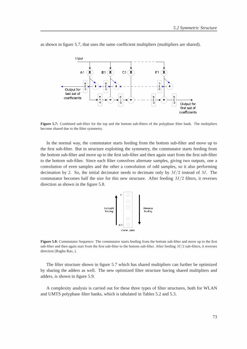
5.2 Symmetric Structure
as shown in figure 5.7, that uses the same coefficient multipliers (multipliers are shared).
Figure 5.7: Combined sub-filter for the top and the bottom sub-filters of the polyphase filter bank. The multipliersbecome shared due to the filter symmetry.
In the normal way, the commutator starts feeding from the bottom sub-filter and move up tothe first sub-filter. But in structure exploiting the symmetry, the commutator starts feeding fromthe bottom sub-filter and move up to the first sub-filter and then again start from the first sub-filterto the bottom sub-filter. Since each filter convolves alternate samples, giving two outputs, one aconvolution of even samples and the other a convolution of odd samples, so it also performingdecimation by 2. So, the initial decimator needs to decimateonly by M/2 instead ofM . Thecommutator becomes half the size for this new structure. After feedingM/2 filters, it reversesdirection as shown in the figure 5.8.
!"# $%&%'%(%%)*+,-.)(%%)*+,Figure 5.8: Commutator Sequence: The commutator starts feeding from the bottom sub-filter and move up to the firstsub-filter and then again start from the first sub-filter to thebottom sub-filter. After feedingM/2 sub-filters, it reversesdirection [Raghu Rao, ].
The filter structure shown in figure 5.7 which has shared multipliers can further be optimizedby sharing the adders as well. The new optimized filter structure having shared multipliers andadders, is shown in figure 5.9.
A complexity analysis is carried out for these three types offilter structures, both for WLANand UMTS polyphase filter banks, which is tabulated in Tables5.2 and 5.3.
73
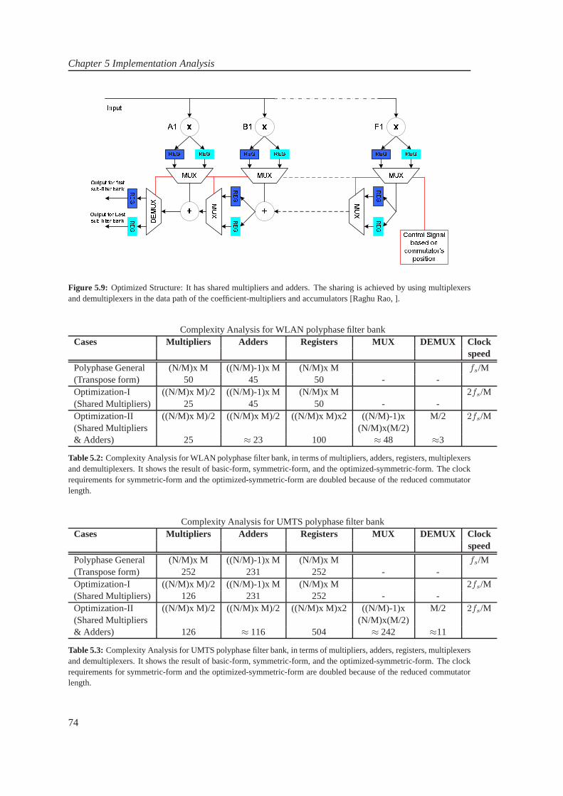
Chapter 5 Implementation Analysis
!" # $ # % & ' ( ) ) # *% % ! !
+ , - . , - /0 1 / 21 3 -3 , 4 5 / 2 6- 7 1 4 8 9 :+ , - . , - /0 1 ; 8 3 -3 , 4 5 / 2 6- 7 1 4 8 9 :Figure 5.9: Optimized Structure: It has shared multipliers and adders.The sharing is achieved by using multiplexersand demultiplexers in the data path of the coefficient-multipliers and accumulators [Raghu Rao, ].
Complexity Analysis for WLAN polyphase filter bankCases Multipliers Adders Registers MUX DEMUX Clock
speed
Polyphase General (N/M)x M ((N/M)-1)x M (N/M)x M fs/M(Transpose form) 50 45 50 - -Optimization-I ((N/M)x M)/2 ((N/M)-1)x M (N/M)x M 2fs/M(Shared Multipliers) 25 45 50 - -Optimization-II ((N/M)x M)/2 ((N/M)x M)/2 ((N/M)x M)x2 ((N/M)-1)x M/2 2fs/M(Shared Multipliers (N/M)x(M/2)& Adders) 25 ≈ 23 100 ≈ 48 ≈3
Table 5.2: Complexity Analysis for WLAN polyphase filter bank, in termsof multipliers, adders, registers, multiplexersand demultiplexers. It shows the result of basic-form, symmetric-form, and the optimized-symmetric-form. The clockrequirements for symmetric-form and the optimized-symmetric-form are doubled because of the reduced commutatorlength.
Complexity Analysis for UMTS polyphase filter bankCases Multipliers Adders Registers MUX DEMUX Clock
speed
Polyphase General (N/M)x M ((N/M)-1)x M (N/M)x M fs/M(Transpose form) 252 231 252 - -Optimization-I ((N/M)x M)/2 ((N/M)-1)x M (N/M)x M 2fs/M(Shared Multipliers) 126 231 252 - -Optimization-II ((N/M)x M)/2 ((N/M)x M)/2 ((N/M)x M)x2 ((N/M)-1)x M/2 2fs/M(Shared Multipliers (N/M)x(M/2)& Adders) 126 ≈ 116 504 ≈ 242 ≈11
Table 5.3: Complexity Analysis for UMTS polyphase filter bank, in termsof multipliers, adders, registers, multiplexersand demultiplexers. It shows the result of basic-form, symmetric-form, and the optimized-symmetric-form. The clockrequirements for symmetric-form and the optimized-symmetric-form are doubled because of the reduced commutatorlength.
74

5.3 Serial Polyphase Filter Bank
Tables 5.2 and 5.3 shows the resource and clock speed requirements for WLAN and UMTSfilter banks. It shows the result of basic-form, symmetric-form, and the optimized-symmetric-form. The clock requirements for symmetric-form and the optimized-symmetric-form are doubledbecause of the reduced commutator length.
5.3 Serial Polyphase Filter Bank
In M-path polyphase filter bank there are M sub-filters, from which M-1 sub-filters are unused atall the time. A more efficient implementation can be achievedby having a serial implementationof polyphase filter bank [Murphy, ]. By doing so, we can get ridof unnecessary sub-filters. MAC(Multiply-Accumulate) can be implementated both in parallel and serial form. In the case of serialMAC, the system have to be clocked at N/M rate, where M is the polyphase sub-filters and N is thenumber of coefficeints in each of the subfilter. A serial MAC implementation structure is shownin figure 5.10 [Murphy, ].
! " # Figure 5.10: Serial polyphase filter bank structure: The incoming data toeach of the sub-filters is fed to a combinedblock of Addressable-Shift-Registers. The set of data that corresponds to the individual sub-filter is accessed bythe pointer addressed by thecounter, which updates at the rate of incoming data. At anycounter value (same ascommutator position), theBranch Index provide the offsets for accessing filter coefficients which are multiplied to thedata-set corresponding to the sub-filter at that time. The data from theAddressable-Shift-Registersand the coefficientfrom theCoefficient Memory are multiplied and accumulated in a serial fasion to have thefinal accumulated results forsub-filter at that time. This process continues for other sub-filters operation as directed bycounter value that providesthe commutator position.
The incoming data to each of the sub-filters is fed to a combined block ofAddressable-Shift-Registers. The set of data that corresponds to the individual sub-filter is accessed by the pointeraddressed by thecounter, which updates at the rate of incoming data. At anycounter value(same as commutator position), theBranch Index provide the offsets for accessing filter coeffi-cients which are multiplied to the data-set corresponding to the sub-filter at that time. The datafrom theAddressable-Shift-Registersand the coefficient from theCoefficient Memory are mul-tiplied and accumulated in a serial fasion to have the final accumulated results for sub-filter atthat time. This process continues for other sub-filters operation as directed bycounter value thatprovides the commutator position.
In the case of parallel MAC structure, the data and the coefficients are fed parallel for the MACoperation, which run at the same clock as the incoming data. In this case there is no need to have
75

Chapter 5 Implementation Analysis
offset from theBranch Index block to access individual coefficients, as all the coefficients areaccessed and multiplied in parallel. A parallel MAC implementation structure is shown in fig-ure 5.10.
Figure 5.11: Parallel MAC structure: The data and the coefficents are fed parallel to the MAC operation, which run atthe same clock as the incoming data. In this case there is no need to have offset from theBranch Index block to accessindividual coefficients as all the coefficients are accessedand multiplied in parallel.
In both of these cases, the output of the filter has to be storedin the individual registers (equalto polyphase sub-filters), which is further processed by theDFT block.
The complexity analysis for Serial Polyphase filter bank implementation with serial and parallelMAC structures is tabulated in Table 5.4.
Complexity Analysis for Serial Polyphase filter bankCases Multipliers Adders Registers Clock Requirement
Serial Polyphase(Serial MAC) 1 1 N fs x (N/M)Serial Polyphase(Parallel MAC) N/M (M/N)-1 N fs
Table 5.4: Complexity Analysis for Serial Polyphase filter bank, interms of multipliers, adders, registers and clockspeed requiremnets.
The table 5.4 shows Area-Speed trade-off between two structures. Serial polyphase structurewith serial MAC requires less resources but demands high clock speed, whereas structure withparallel MAC requires large resources but low clock speed.
5.4 Conclusion
we have analyzed the structure of polyphase channelizer andpresented different structural tech-niques to carry out the implementation. In this regard, general polyphase structure, optimized
76

5.5 FIR Filtering
structures - symmetric property based structure, adder shared structure, serial polyphase struc-tures with serial and parallel MAC are considered. Complexity Analysis is carried out to choosethe least expensive solution amoung them. Based on Tables 5.2, 5.3 and 5.4, serial polyphasestructure with parallel MAC is selected for the final implementation. In an M channels filterbank,each sub-filter operates at 1/M of the input sample-rate (fs), we take advantage of this propertyand share the multipliers and the multi-operand adder of onesub-filter among all the sub-filters inthe filter bank. This results in a clock requirement to be sameas input sampling rate. Thus wecome up withtime-constraint for implementation, which is equal to input sampling rate (fs).
We have discussed the system level modifications and optimizations of the polyphase chan-nelizer having focus on polyphase filter bank. As the basic block of the polyphase filter bank isa sub-filter, which is a FIR filter as well, so in the next sections, we look further into differentimplementation structures for the basic FIR filter, which later on, is used in the polyphase filterbank.
5.5 FIR Filtering
A FIR filter computes the discrete convolution of an input anda finite length filter response. Thisconvolution can be written as
y[n] =
N−1∑
k=0
h[k]x[n − k] (5.1)
where N is the length of the filter response and is referred to as the number of taps in the filter.
Several different algorithms or filtering techniques are investigated for implementing a FIRfilter including:
• FIR filtering using parallel multipliers and accumulators
• A bit-level systolic array
• Distributed Arithmetic
• Fast FIR algorithms
• Frequency domain filtering
• Multiplier-less FIR filter (SOPOT)
In the next sections, each of these different types is brieflyexplained, followed by their struc-tures and optimizations.
5.5.1 Parallel Multipliers and Accumulators
The most direct realization of a FIR filter is to calculate theoutput using parallel multipliers andaccumulators (MACs). The parallel MAC structure is illustrated in Figure 5.12, and is deriveddirectly from the FIR convolution in equation 5.1 [Alan V. Oppenheim, 1999]. In this structure,
77
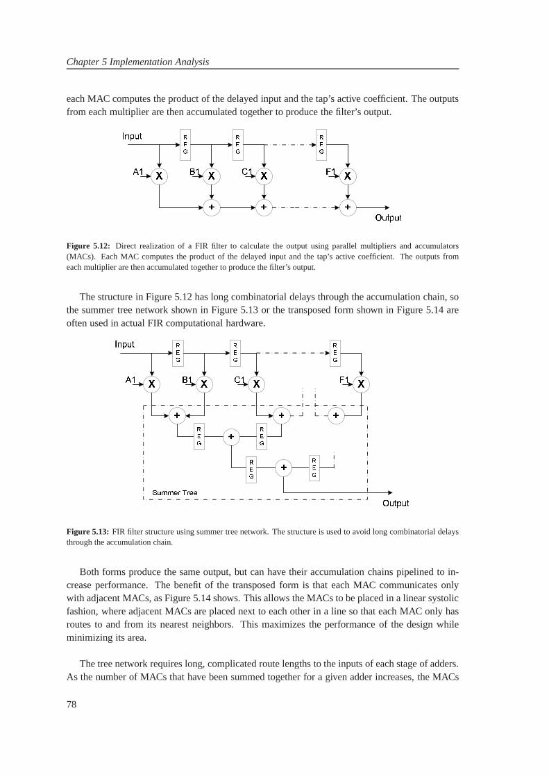
Chapter 5 Implementation Analysis
each MAC computes the product of the delayed input and the tap’s active coefficient. The outputsfrom each multiplier are then accumulated together to produce the filter’s output.
Figure 5.12: Direct realization of a FIR filter to calculate the output using parallel multipliers and accumulators(MACs). Each MAC computes the product of the delayed input and the tap’s active coefficient. The outputs fromeach multiplier are then accumulated together to produce the filter’s output.
The structure in Figure 5.12 has long combinatorial delays through the accumulation chain, sothe summer tree network shown in Figure 5.13 or the transposed form shown in Figure 5.14 areoften used in actual FIR computational hardware.
! " " # $ % $ # #
Figure 5.13: FIR filter structure using summer tree network. The structure is used to avoid long combinatorial delaysthrough the accumulation chain.
Both forms produce the same output, but can have their accumulation chains pipelined to in-crease performance. The benefit of the transposed form is that each MAC communicates onlywith adjacent MACs, as Figure 5.14 shows. This allows the MACs to be placed in a linear systolicfashion, where adjacent MACs are placed next to each other ina line so that each MAC only hasroutes to and from its nearest neighbors. This maximizes theperformance of the design whileminimizing its area.
The tree network requires long, complicated route lengths to the inputs of each stage of adders.As the number of MACs that have been summed together for a given adder increases, the MACs
78

5.5 FIR Filtering
Figure 5.14: Transpose-FIR filter structure. The structure is used to avoid long combinatorial delays through theaccumulation chain.
grow farther apart. This prohibits a simple linear distribution of MAC cells and slows the design’sperformance due to the long routes.
One problem with the transposed form of the parallel MAC filter is that it requires a largefan-out on theinput signals, as they must connect to every MAC. To reduce this fan-out whilemaintaining pipelining in the accumulation chain and allowing the MACs to be placed in a linearsystolic fashion, an additional stage of pipelining in boththe inputs and outputs of each MAC canbe introduced into the direct filter structure as shown in Figure 5.15.
Figure 5.15: Direct filter structure having additional stage of pipelining in both the inputs and outputs of each MAC,inorder to reduce large fan-out on theinput signal while maintaining pipelining in the accumulation chain and allowingthe MACs to be placed in a linear systolic fashion.
A frequent method used to decrease the area of a parallel MAC approach to FIR filtering is toincrease the number of taps computed per MAC. This is the technique used in the custom VLSIchip [Moeller and Martinez, 1999] [David R. Martinez and Teitelbaum, 2000].
A block diagram of the custom VLSI chip’s architecture is shown in Figure 5.16 [Moeller and Martinez, 1999][David R. Martinez and Teitelbaum, 2000]. It consists of 64 MAC units. Each MAC unit containsa multiplier, accumulator and intermediate storage memory, and two banks of coefficient memory.The two banks of coefficient memory allows one set of coefficients to be active and is used bythe multipliers while a new set can be loaded into the other coefficient bank. Once the new sethas been loaded, it can now become active, allowing the chip to instantly change from one set ofcoefficients to another. Each MAC, by using the accumulator and intermediate storage memory, iscapable of forming the products of the current chip input andup to eight filter taps (i.e. eight co-efficients). These products are accumulated together as required within the MAC, and then added
79

Chapter 5 Implementation Analysis
!"#$%&%& ' () !"#$%&%& ' ' * #+ ,- ./ $
Figure 5.16: Block diagram of the custom VLSI chip’s architecture. It consists of 64 MAC units. If the MACs areoperating in their eight tap mode, they must run at a clock rate eight times the input sample rate so that all eighttaps’ products are computed each time a new input arrives. Inthis mode, the 64 MACs can compute a 512-tap realfilter [Moeller and Martinez, 1999] [David R. Martinez and Teitelbaum, 2000].
to the other MACs’ results when a new input is present. If the MACs are operating in their eighttap mode, they must run at a clock rate eight times the input sample rate so that all eight taps’products are computed each time a new input arrives. In this mode, the 64 MACs can compute a512-tap real filter [Moeller and Martinez, 1999] [David R. Martinez and Teitelbaum, 2000].
One variation [Moeller, 1999] of this technique is shown in Figure 5.17. In this structure, asingle multiplier is re-used eight times to compute the product of eightinput values multiplied byeight coefficients for each input into the filter. An eight-word deep RAM stores the eight coeffi-cients for the tap, and a seven-word long shift register stores theinput values. This architecture issimilar to the one used in the custom VLSI chip (Figure 5.16),except that shift registers have beenused to store multiple input values for each MAC instead of RAM storing the multiplier’s outputs.The result is the same except that storing multiple inputs per tap requires less memory since theinputs are only 16-bits long versus the 24-bit multiplier outputs.
The shift registers are loaded with a new value at the beginning of each eight-clock cycle. Theshift registers are then fed their outputs back into their inputs for the next seven clock cycles. Thismoves the input that was shifted into the register at the beginning of the eight clock cycles to thesecond shift register position at the beginning of the next eight clock cycles so that the next newvalue is loaded into the first position. After eight clock cycles, this input becomes the new valueto the next MAC’s shift registers. At the same time, the shiftregisters are arranged so that eightconsecutive input values are supplied to the multiplier to be multiplied by eight consecutive coef-ficient values. These will be added together by the final accumulator shown in Figure 5.17.
The output of the first two MACs’ shift registers and coefficient registers (i.e. the multiplierinputs) are shown in Table 5.5, for two-tap MACs. With eight-tap MACs, the movement of inputsthrough the shift registers produces the same effect with 64multipliers as if 512 multipliers hadbeen used with a clock rate equal to the sample rate.
80
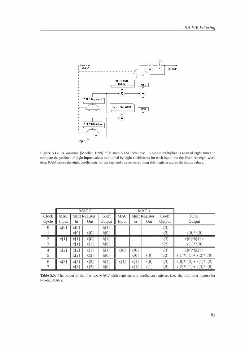
5.5 FIR Filtering
! "#$%&
'()* + ,-./ '0) 12* +,-./
Figure 5.17: A variation [Moeller, 1999] of custom VLSI technique. A single multiplier is re-used eight times tocompute the product of eightinput values multiplied by eight coefficients for each input into the filter. An eight-worddeep RAM stores the eight coefficients for the tap, and a seven-word long shift register stores theinput values.
MAC 0 MAC 1Clock MAC Shift Register Coeff MAC Shift Register Coeff FinalCycle Input In Out Output Input In Out Output Output
0 x[0] x[0] h[1] h[3]1 x[0] x[0] h[0] h[2] x[0]*h[0]
2 x[1] x[1] x[0] h[1] h[3] x[0]*h[1] +3 x[1] x[1] h[0] h[2] x[1]*h[0]
4 x[2] x[2] x[1] h[1] x[0] x[0] h[3] x[0]*h[2] +5 x[2] x[2] h[0] x[0] x[0] h[2] x[1]*h[1] + x[2]*h[0]
6 x[3] x[3] x[2] h[1] x[1] x[1] x[0] h[3] x[0]*h[3] + x[1]*h[2]7 x[3] x[3] h[0] x[1] x[1] h[2] x[2]*h[1] + x[3]*h[0]
Table 5.5: The output of the first two MACs’ shift registers and coefficient registers (i.e. the multiplier inputs) fortwo-tap MACs.
81

Chapter 5 Implementation Analysis
5.5.2 Bit-level Systolic Array
It is a fully-efficient bit-level systolic structure by [Chin-Liang Wang and Chen, 1988]. With thistechnique, single-bit processors compute each tap’s multiplication partial products and accumu-late tap outputs together in a systolic array. As inputs propagate through the array, filtered out-puts are produced. The systolic nature of this approach lends itself well to VLSI, and would beideal for a FPGA if it was area-efficient, as it would limit therouting requirements in the FPGAto local connections between CLBs. The details of the mathematical derivations can be foundin [Chin-Liang Wang and Chen, 1988]
This technique did not turn out to be efficient in a FPGA architecture (detials are in the nextchapter). It is presented to show the differences between architectures optimized for a FPGA’scoarse-grained structure versus architectures optimizedat the transistor level for a VLSI ap-proach [Moeller, 1999].
5.5.3 Distributed Arithmetic (DA)
This section describes Distributed Arithmetic (DA), and isbased on information presentedin [Xilinx, ] [Moeller and Martinez, 1999].
Distributed Arithmetic works by distributing the bit arithmetic of the sum-of-products (alsocalled the vector dot product) used to calculate the FIR filter output given in Equation5.1. Thisequation will be re-written as
y[n] =
N−1∑
k=0
AkXk(n) (5.2)
whereAk = h[k].
A FIR filter is typically implemented with some variation of Figure 5.12 or Figure 5.14, wherea summation of the results of N multipliers each calculatingan AkXk(n) product produce theoutput for a givenn input.
The number format used in the custom VLSI chip and in the FPGA design is 2’s complementfractional fixed-point [Moeller, 1999]. In this format, thebinary point is to the right of the mostsignificant bit so that the most significant bit of a number represents -1, and each subsequent bitrepresents a power of1/2. Using this format, the variable may be written as
Xk = −Xk0 +
B−1∑
b=1
Xkb2−b (5.3)
wherexkb is thebth bit of xk , and B is the number of bits in the input variable.
82

5.5 FIR Filtering
Substituting Equation 5.3 into Equation 5.2 gives (n has been dropped, as we are only con-cerned with a single given output sample)
y =
N−1∑
k=0
Ak
(
−Xk0 +
B−1∑
b=1
Xkb2−b
)
(5.4)
which when rewritten, gives
y = −N−1∑
k=0
Xk0Ak +B−1∑
b=1
2−b
(
N−1∑
k=0
XkbAk
)
(5.5)
Explicitly writing the summation results in the following DA equation:
y = −[
X00A0 + X10A1 + ....... + X(N−1)0AN−1
]
= +[
X01A0 + X11A1 + ....... + X(N−1)1AN−1
]
2−1
....
= +[
X0(B−1)A0 + X1(B−1)A1 + ....... + X(N−1)(B−1)AN−1
]
2B−1
(5.6)
Each multiplication of aXkb term and anAk term is the product of a coefficient word with aninput bit. This can be implemented by using an AND gate between each bit of the coefficient wordand the input bit. Each scaling factor2−i can be implemented by shifting the data to be scaledright i bits. Equation 5.6, therefore becomes the summation of the scaled summation of a seriesof AND gates. This operation could be performed in parallel or bit-serially, where on each clockcycle a single bit from everyXk is multiplied by the correspondingAk, forming one bracketedterm in Equation 5.6. These partial products are then accumulated together with the appropriatescaling to produce a final multiplier output. An example of bit-serial multiplication for a singlecoefficient and input is shown in figure 5.18 [Moeller and Martinez, 1999].
! " # $% &' ! #$()*+ , -./ 012 34567450 78 649:; <5== = =
Figure 5.18: Bit-serial multiplication: The partial products obtainedby multiplying each bit of input with the filtercoefficient through AND gate, are accumulated together withthe appropriate scaling to produce a final multiplieroutput.
Figure 5.18 illustrates, on each clock cycle a single partial product consisting of one bit ofthe input multiplied by the coefficient is produced. This partial product is then added to an accu-mulating sum of partial products, which has been shifted right one bit (multiplied by 1/2). This
83
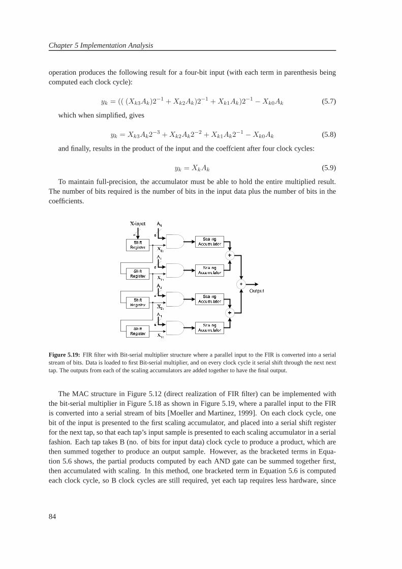
Chapter 5 Implementation Analysis
operation produces the following result for a four-bit input (with each term in parenthesis beingcomputed each clock cycle):
yk = (( (Xk3Ak)2−1 + Xk2Ak)2
−1 + Xk1Ak)2−1 − Xk0Ak (5.7)
which when simplified, gives
yk = Xk3Ak2−3 + Xk2Ak2
−2 + Xk1Ak2−1 − Xk0Ak (5.8)
and finally, results in the product of the input and the coeffcient after four clock cycles:
yk = XkAk (5.9)
To maintain full-precision, the accumulator must be able tohold the entire multiplied result.The number of bits required is the number of bits in the input data plus the number of bits in thecoefficients.
! !
" " # #
$$ $
Figure 5.19: FIR filter with Bit-serial multiplier structure where a parallel input to the FIR is converted into a serialstream of bits. Data is loaded to first Bit-serial multiplier, and on every clock cycle it serial shift through the next nexttap. The outputs from each of the scaling accumulators are added together to have the final output.
The MAC structure in Figure 5.12 (direct realization of FIR filter) can be implemented withthe bit-serial multiplier in Figure 5.18 as shown in Figure 5.19, where a parallel input to the FIRis converted into a serial stream of bits [Moeller and Martinez, 1999]. On each clock cycle, onebit of the input is presented to the first scaling accumulator, and placed into a serial shift registerfor the next tap, so that each tap’s input sample is presentedto each scaling accumulator in a serialfashion. Each tap takes B (no. of bits for input data) clock cycle to produce a product, which arethen summed together to produce an output sample. However, as the bracketed terms in Equa-tion 5.6 shows, the partial products computed by each AND gate can be summed together first,then accumulated with scaling. In this method, one bracketed term in Equation 5.6 is computedeach clock cycle, so B clock cycles are still required, yet each tap requires less hardware, since
84

5.5 FIR Filtering
only one master scaling accumulator is now necessary. The new FIR structure is shown in Fig-ure 5.20 [Moeller and Martinez, 1999].
! ! " " # # $
$ $Figure 5.20: FIR filter with Bit-serial multiplier structure where a parallel input to the FIR is converted into a serialstream of bits. In this structure, only one scaling accumulator is used after adding partial products from all the taps.
To maintain full precision in this case, the scaling accumulator is now required to hold the num-ber of bits in the input plus the number of bits in the coefficients plus the number of bits added dueto word growth through the adder stages (1 bit per stage).
If the coefficients for the filter are constant, then the output of the summer tree depends solelyon the single-bit inputs to each tap. With this being the case, the storage registers for the coeffi-cients, the AND gates, and the summer tree can all be replacedby a single look-up-table addressedby the single-bit shift register outputs as shown in Figure 5.21.
With four taps as shown in Figure 5.21, a LUT with 16 entries isrequired. Each 4-bit addressinto the LUT can be thought of as being a sum of coefficients: ifa particular address bit is high,then that address’ sum should include the corresponding coefficient. To keep the output of theLUT at full precision, the LUT should be two bits larger than the size of the coefficients to accom-modate for word growth through the additions.
Implementation considerations
The 16x1 RAM units within the Xilinx CLBs are ideal candidates for this sort of DA scheme. Onebit of a single 4-input LUT can fit into one of these units with no unused logic [Moeller and Martinez, 1999].For FIR filters larger than 4-taps, the filter can be broken into four tap groups, each constructed asshown in Figure 5.21. For example, a 8-tap FIR is shown in figure 5.22. To eliminate overflow,each adder stage must grow by one bit, and the scaling accumulator must also grow accordinglyin size (the scaling accumulator could drop the lower bits inits accumulation if less precision isrequired).
85

Chapter 5 Implementation Analysis
! "
#$ %&'(()$*+,-.Figure 5.21: Look-up Table based Serial distributed FIR structure.
/ 0 1 2 0 13 4 5 6 789: 4 4 ; < ; 65 = > ?3 @ 7A= B C 9 DE F GH I J KL M N OP 2 0 1QR R S N 0 2T U V WX3 @ 7A= B C 9 D3 @ 7A= B C 9 D3 @ 7A= B C 9 D3 @ 7A= B C 9 D M N OP 2 0 1QR R S N 0 2T U V WX3 @ 7A= B C 9 D3 @ 7A= B C 9 D3 @ 7A= B C 9 D
YFigure 5.22: 8-Tap Serial Distributed FIR filter structure. Two 4-Tap Serial Distributed FIR filters are used to have a8-Tap filter.
86

5.5 FIR Filtering
Although larger LUTs could be used with less adders, LUTs larger than four inputs do not savespace. For example, a five-input LUT would require 32- entries and take up two 16x1 RAM units(an entire slice). However, if these two 16x1 RAM units were used separately, they could each beaddressed by four taps, allowing an entire slice to handle eight taps. The extra adder needed tosum the two four-input LUTs together would not significantlyincrease the area enough to justifya five-input LUT.
Parallel Distributed Arithmetic
A benefit of distributed arithmetic is that it easily allows atrade-off to be made between the filter’sarea and performance. By doubling the filter’s area, the filter’s throughput or sample rate can bedoubled without changing the clock rate that the individualfilter components operate at. In theserial distributed arithmetic (SDA) designs discussed before, a clock rate B times the sample rateis required, as one clock cycle is needed to look up a partial product for each bit of x. However,by taking advantage of a feature inherent in the DA equation,Equation 5.6, fewer clock cycles canbe required per input sample. Presently, one term in the equation has been computed per clockcycle. However, any number of terms can be computed per clockcycle (referred to as paralleldistributed arithmetic, or PDA). For example, if two terms are computed per clock cycle, then B/2clock cycles are required to compute an output.
!" #$ # #% & & & $ '() * + ) , - ./ 0 1 2 3 4 5 6 3 4 / 6 7 5 3 8 9 : ; 4
$ < = > > ! #? #@ #% & & & ' $ A B A A C D C + Figure 5.23: 2-Bit Parallel Distributed Arithmetic FIR. By computing 2 terms per clock cycle, then B/2 clock cyclesare required to compute an output.
To compute two terms per clock cycle, two identical SDA FIR filters as described above mustbe constructed. Each filter will compute one term in Equation5.6 so that two terms are computedper clock cycle. One filter will compute outputs for even input sample bits, and the other filter willcompute outputs for odd input sample bits. For example, on the first clock cycle, the first filterwill compute the output term associated withXk0 while the other filter computes the output termassociated withXk1. These outputs are then added together, being the first filter’s output (the bit0 term) scaled by 1/2, and then sent to the scaling accumulator. On each clock cycle, the scalingaccumulator scales its registered accumulation by 1/4 to accommodate for the fact that it is han-dling two partial products per clock cycle instead of one. The 2-bit PDA approach requires twiceas much area as the serial approach, but has twice the performance, and is illustrated in Figure 5.23.
87

Chapter 5 Implementation Analysis
! ! " " # # $ % $ % $ % $ %
$ % $ % $ %
& '& (& )& *& +& ,& -& .& / &
0 1 2 0 3 2Figure 5.24: (a). A single-bit PDA and (b). A 8-bit fully PDA FIR filter.
For the fully parallel 8-bit PDA FIR filter implementation, the 8-bit input sample is partitionedinto eight 1-bit sub-samples so as to achieve maximum speed.Figure 5.24 [Al-Haj, 2004] showsthe ultimate fully parallel PDA FIR filter, where all 8 input bits are computed in parallel and thensummed by a binary-tree like adder network. The lower input to each adder is scaled down by afactor of 2. No scaling accumulator is needed in this case, since the output from the adder tree isthe entire sum of products.
5.5.4 Fast FIR Algorithm
The class of fast FIR algorithms (FFA) attempt to increase the parallelism of the FIR struc-ture without a linear increase in area [Parker and Parhi, 1997] [Jin-Cyun Chung and Wang., 1998].Traditionally, to double the throughput of a FIR filter without increasing the clock rate of the filteritself, the filter area would have to be doubled.
Doubling the throughput of a FIR filter without changing its internal clock rate means that twooutputs are to be calculated each clock cycle. These two outputs will be referred to asy[2j] andy[2j +1]. Producing two outputs per clock cycle would require two inputs per clock cycle as well,x[2j] andx[2j + 1]. This leads to the following set of equations:
x0[j] = x[2j]
x1[j] = x[2j + 1]
y0[j] = y[2j]
y1[j] = y[2j + 1]
wherex0 andy0 represent the even inputs and outputs, andx1 andy1 represent the odd inputsand outputs.
88

5.5 FIR Filtering
Two polyphase decompositions of the filter will be required,one containing the even samples ofthe original filter, the other the odd:
h0[k] = h[2k]
h1[k] = h[2k + 1]
whereh[n] is the original filter, and N is the length of the original filter. The above equationsgive the following z-transforms:
X = X0 + X1z−1
H = H0 + H1z−1
Y = Y0 + Y1z−1
which leads to the following two-parallel polyphase representation of the FIR filter:
Y = X.H
= (X0 + X1z−1)(H0 + H1z
−1)
= X0H0 + (X0H1 + X1H0)z−1 + X1H1z
−2 (5.10)
Y0 = X0H0 + X1H1z−2
Y1 = X0H1 + X1H0
Equation 5.10 indicates that to double the throughput of theoverall FIR filter two of each ofthe length N/2 polyphase filters would be required as shown inFigure 5.25, resulting in an overallfilter with twice as many taps as the original filter (four N/2 length filters).
Figure 5.25: Traditional Two-parallel FIR Filter Implementation. To double the throughput of the overall FIR filter,two of each of the length N/2 polyphase filters are required.
Two input samples are collected at a time and passed into the filter structure as illustrated inFigure 5.25, which produces two output samples. Each filter block shown in the Figure 5.25 isrunning as fast as the original filter, however, the throughput has been doubled. The FFA approachtakes advantage of a rewriting of the polyphase equations derived from Equation 5.10:
89

Chapter 5 Implementation Analysis
Y = X0H0 + (X0H1 + X1H0)z−1 + X1H1z
−2
= X0H0 + [(X0 + X1)(H0 + H1) − X0H0 − X1H1]z−1 + X1H1z
−2 (5.11)
which implies that
Y0 = X0H0 + X1H1z−2
Y1 = (X0 + X1)(H0 + H1) − X0H0 − X1H1
The structure that implements Equation 5.12 is shown in Figure 5.26 for the same overall filterinputs and outputs. This filter only requires 1.5 times as many taps as the original, non-parallel,filter, although the coefficients for the middle FIR element in this case must be pre-computedbefore being loaded into the FIR element. This is not an issuefor most applications, as such acomputation can be performed external to the filter.
Figure 5.26: Two-Parallel FFA Implementation
5.5.5 Frequency Domain Filtering
Instead of using convolution to calculate the output response for a FIR filter, the filtering can beperformed in the frequency domain. Convolution in the time domain is simply a multiplicationoperation in the frequency domain, so such an operation requires a transformation from the timedomain to the frequency domain by a fast Fourier transform (FFT), a point multiplication of theinput signal’s spectrum by the filter’s spectrum, and a transformation back to the time domain byan inverse fast Fourier transform (IFFT). The benefit of thistechnique is that it requires much lesscomputational hardware than any of the approaches discussed so far using convolution. A FFT’scomputational requirements scales on the order oflog2N versus N for convolution approaches.
The FFT is derived from the discrete Fourier transform (DFT), which is used to transform dis-crete time waveforms into discrete frequency spectrums [Alan V. Oppenheim, 1999] [Groginsky and Works., ].The DFT is defined by
x[k] =
N−1∑
n=0
x[n]W knN (5.12)
where
W knN = e−j(2π/N)kn (5.13)
90
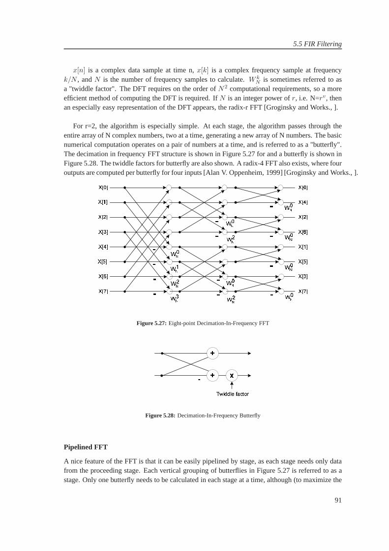
5.5 FIR Filtering
x[n] is a complex data sample at time n,x[k] is a complex frequency sample at frequencyk/N , andN is the number of frequency samples to calculate.W k
N is sometimes referred to asa "twiddle factor". The DFT requires on the order ofN2 computational requirements, so a moreefficient method of computing the DFT is required. IfN is an integer power ofr, i.e. N=rv, thenan especially easy representation of the DFT appears, the radix-r FFT [Groginsky and Works., ].
For r=2, the algorithm is especially simple. At each stage, the algorithm passes through theentire array of N complex numbers, two at a time, generating anew array of N numbers. The basicnumerical computation operates on a pair of numbers at a time, and is referred to as a "butterfly".The decimation in frequency FFT structure is shown in Figure5.27 for and a butterfly is shown inFigure 5.28. The twiddle factors for butterfly are also shown. A radix-4 FFT also exists, where fouroutputs are computed per butterfly for four inputs [Alan V. Oppenheim, 1999] [Groginsky and Works., ].
Figure 5.27: Eight-point Decimation-In-Frequency FFT
Figure 5.28: Decimation-In-Frequency Butterfly
Pipelined FFT
A nice feature of the FFT is that it can be easily pipelined by stage, as each stage needs only datafrom the proceeding stage. Each vertical grouping of butterflies in Figure 5.27 is referred to as astage. Only one butterfly needs to be calculated in each stageat a time, although (to maximize the
91

Chapter 5 Implementation Analysis
sample rate), each stage must have a butterfly calculated each clock cycle. Therefore, the FFT canbe built in a pipelined fashion, with each stage handled by a single pipelined butterfly.
Each pipelined butterfly needs shift register storage wordslong (where m is the stage number,with 0 being the right-most stage) to align its inputs and outputs correctly. For example, the firststage has butterflies that process inputs four samples apartin time. A shift register four wordslong is required to store the first four inputs, then output those four inputs to the top of that stage’sbutterfly as the next four inputs arrive at the bottom of the butterfly to compute the correct butterflyoutputs. The top output of the butterfly are sent to the next stage while the bottom outputs are putinto the shift register, which are then shifted out after thefour butterflies have been computed. Anexample of a pipeline module is shown in Figure 5.29 [Groginsky and Works., ], and an eight-pointpipelined FFT architecture is shown in Figure 5.30 [Groginsky and Works., ].
! " # ! $% & ' ! # ' # ( ) * ( + , & $- (
Figure 5.29: Pipelined FFT Butterfly Module
The twiddle factors can be arranged so that they may be sent toall of the modules from a com-mon memory if they are retrieved at the correct time, reducing memory requirements [Groginsky and Works., ].
. /0 1 2 /3 1 45 6 4 7 21 . /0 1 2 /3 1 45 6 4 7 21 . /0 1 2 /3 1 45 6 4 7 218 9 /4 4 21 : ; < = 6 > ? = 6 > ; @ 1Figure 5.30: 8-Point Pipelined FFT Architecture Block Diagram
FFT Covolution
Performing convolution with a FFT (i.e. transforming to thefrequency domain, multiplying, andtransforming back to the time domain) requires a FFT at leasttwice as large as the length of the fil-ter to avoid time-aliasing in computing the DFT of the filter coefficients [Alan V. Oppenheim, 1999].
92

5.5 FIR Filtering
If a filter is N taps long, the FFT of the filter will have to be 2N points (with zero padding used toextend the N taps to 2N inputs for a 2N-point FFT). The convolution is performed by retrieving ablock of N inputs, performing a 2N-point FFT (with zero-padding filling out the inputs) on them,multiplying them by the 2N filter frequency components previously transformed to the frequencydomain by FFT, and performing an IFFT on the multiplication outputs. However, since only Ninputs were taken and N outputs should be produced from the filter for a given block, and the2N-point IFFT produces 2N outputs, only the last N IFFT outputs should be used as filter outputs,as the first N IFFT outputs do not represent correct values of the convolution of the filter and theblock of inputs [Alan V. Oppenheim, 1999]. This process is termed overlap-save.
A fixed-point FFT requires a considerable amount of rounding, as each stage has a multiplierthat increases the stage’s bit-length drastically. Rounding is required to reduce the stage’s outputto a manageable size. The noise analysis for a fixed-point FFTis complex, and is described indetail in [Alan V. Oppenheim, 1999] and [Liu, 1975]. The important result is that each stage’sbutterfly’s outputs require a scaling factor of 1/2 to keep their adders from overflowing, which alsoreduces the final total amount of noise at the output.
5.5.6 Multiplier-less FIR filter
There are many structures for implementing FIR filters in theliterature. Figure 5.31 shows thedirect form implementation of the FIR filter. The filter coefficients and the registers (denotedby R) form the tapped-delay line of the FIR filter. For low datathroughput rate, the coefficientmultiplications can be implemented using the multipliers in a digital signal processor (DSP).
Figure 5.31: Direct Form implmentation of general FIR filter
For high data throughput, usually in traditional VLSI design, hardware multipliers are usedwhich are expensive in terms of hardware resources and powerconsumption, So in order to solvethis problem Sum Of Power Of Two (SOPOT) coeffient representation is used. Where SOPOTcan be implemented by shift and add operations. The hardwarecomplexities of these multiplier-less FIR filter is thus very low. Another efficient method for reducing hardware complexity is toemploy the hardware multiplier block technique explained in [A.G. Dempster, 1995].
93
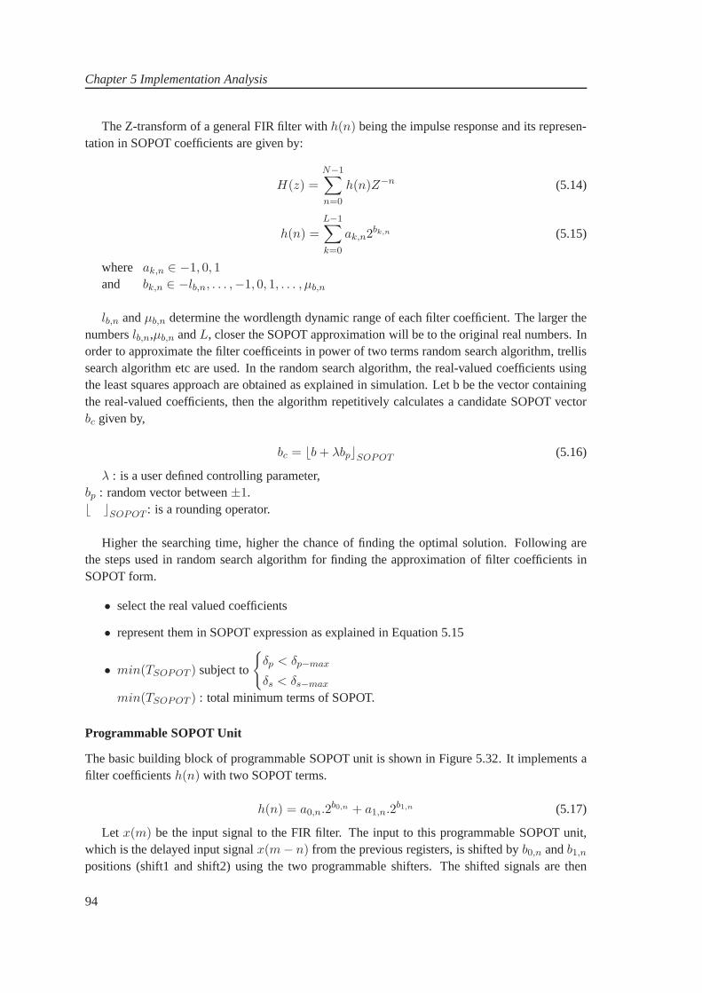
Chapter 5 Implementation Analysis
The Z-transform of a general FIR filter withh(n) being the impulse response and its represen-tation in SOPOT coefficients are given by:
H(z) =
N−1∑
n=0
h(n)Z−n (5.14)
h(n) =
L−1∑
k=0
ak,n2bk,n (5.15)
where ak,n ∈ −1, 0, 1
and bk,n ∈ −lb,n, . . . ,−1, 0, 1, . . . , µb,n
lb,n andµb,n determine the wordlength dynamic range of each filter coefficient. The larger thenumberslb,n,µb,n andL, closer the SOPOT approximation will be to the original realnumbers. Inorder to approximate the filter coefficeints in power of two terms random search algorithm, trellissearch algorithm etc are used. In the random search algorithm, the real-valued coefficients usingthe least squares approach are obtained as explained in simulation. Let b be the vector containingthe real-valued coefficients, then the algorithm repetitively calculates a candidate SOPOT vectorbc given by,
bc = ⌊b + λbp⌋SOPOT (5.16)
λ : is a user defined controlling parameter,bp : random vector between±1.⌊ ⌋SOPOT : is a rounding operator.
Higher the searching time, higher the chance of finding the optimal solution. Following arethe steps used in random search algorithm for finding the approximation of filter coefficients inSOPOT form.
• select the real valued coefficients
• represent them in SOPOT expression as explained in Equation5.15
• min(TSOPOT ) subject to
δp < δp−max
δs < δs−max
min(TSOPOT ) : total minimum terms of SOPOT.
Programmable SOPOT Unit
The basic building block of programmable SOPOT unit is shownin Figure 5.32. It implements afilter coefficientsh(n) with two SOPOT terms.
h(n) = a0,n.2b0,n + a1,n.2b1,n (5.17)
Let x(m) be the input signal to the FIR filter. The input to this programmable SOPOT unit,which is the delayed input signalx(m − n) from the previous registers, is shifted byb0,n andb1,n
positions (shift1 and shift2) using the two programmable shifters. The shifted signals are then
94
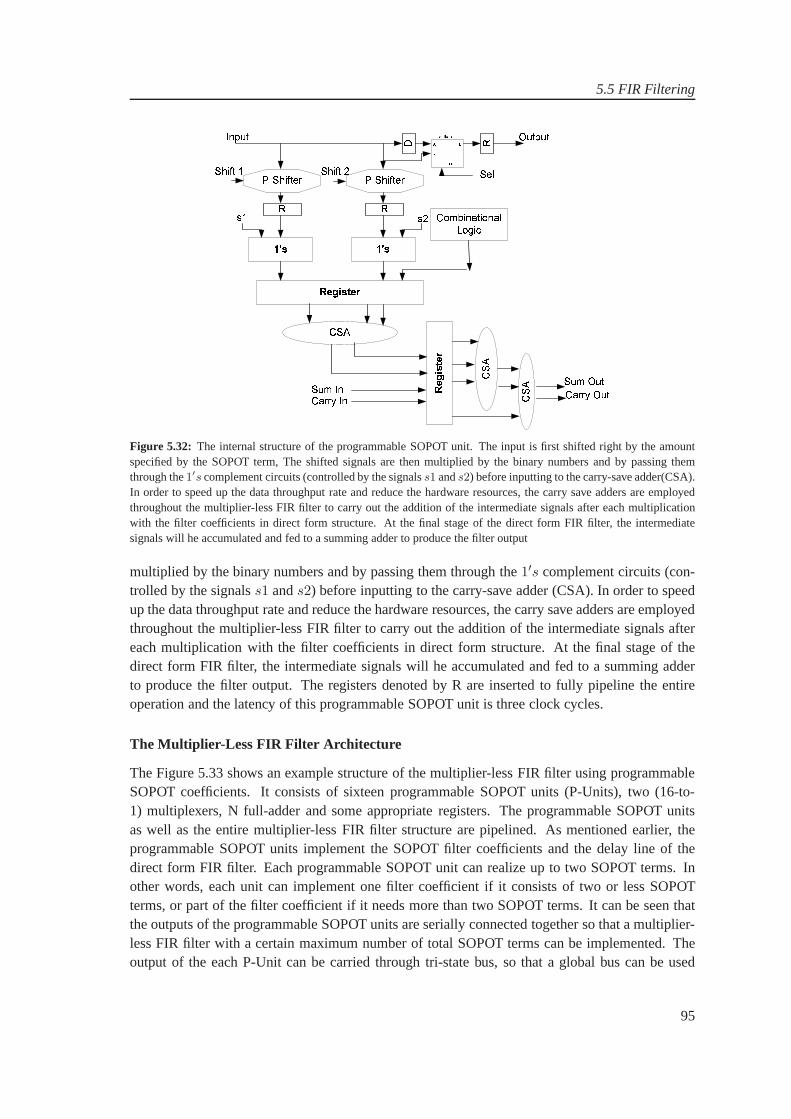
5.5 FIR Filtering
!"#$ %&' %&'
( )*+,-.- / . /
, * , 0, 1 0 , 1 *
2324 56 789: ; <= >? <@A @ B 0 ,+ ,
Figure 5.32: The internal structure of the programmable SOPOT unit. The input is first shifted right by the amountspecified by the SOPOT term, The shifted signals are then multiplied by the binary numbers and by passing themthrough the1′s complement circuits (controlled by the signalss1 ands2) before inputting to the carry-save adder(CSA).In order to speed up the data throughput rate and reduce the hardware resources, the carry save adders are employedthroughout the multiplier-less FIR filter to carry out the addition of the intermediate signals after each multiplicationwith the filter coefficients in direct form structure. At the final stage of the direct form FIR filter, the intermediatesignals will he accumulated and fed to a summing adder to produce the filter output
multiplied by the binary numbers and by passing them throughthe1′s complement circuits (con-trolled by the signalss1 ands2) before inputting to the carry-save adder (CSA). In order tospeedup the data throughput rate and reduce the hardware resources, the carry save adders are employedthroughout the multiplier-less FIR filter to carry out the addition of the intermediate signals aftereach multiplication with the filter coefficients in direct form structure. At the final stage of thedirect form FIR filter, the intermediate signals will he accumulated and fed to a summing adderto produce the filter output. The registers denoted by R are inserted to fully pipeline the entireoperation and the latency of this programmable SOPOT unit isthree clock cycles.
The Multiplier-Less FIR Filter Architecture
The Figure 5.33 shows an example structure of the multiplier-less FIR filter using programmableSOPOT coefficients. It consists of sixteen programmable SOPOT units (P-Units), two (16-to-1) multiplexers, N full-adder and some appropriate registers. The programmable SOPOT unitsas well as the entire multiplier-less FIR filter structure are pipelined. As mentioned earlier, theprogrammable SOPOT units implement the SOPOT filter coefficients and the delay line of thedirect form FIR filter. Each programmable SOPOT unit can realize up to two SOPOT terms. Inother words, each unit can implement one filter coefficient ifit consists of two or less SOPOTterms, or part of the filter coefficient if it needs more than two SOPOT terms. It can be seen thatthe outputs of the programmable SOPOT units are serially connected together so that a multiplier-less FIR filter with a certain maximum number of total SOPOT terms can be implemented. Theoutput of the each P-Unit can be carried through tri-state bus, so that a global bus can be used
95

Chapter 5 Implementation Analysis
!"#$#%&
' ()' ()' ()' ()
Figure 5.33: The multiplier-less FIR architecture which consists of sixteen programmable SOPOT units (P-Units), two(16 − to − 1) multiplexers, N full-adder and some appropriate registers. The outputs of the programmable SOPOTunits are serially connected together so that a multiplier-less FIR filter with a certain maximum number of total SOPOTterms can be implemented.
to reduce the routing area. (16-to-1) multiplexers are usedfor each sum and carry, which can beconfigured by usingSel(3:0)as control signal.
Complexity Analysis of Multiplier-less FIR filter
The P-unit consists primarily of shifters and adders, so thecomplexity of each P-unit depends onthese processing elements. The Programmable shifter is shown in Figure 5.34. It is used to shiftthe input signal from (0-31) bits to the right. It consists of5, (2-to-1) mux arranged in5 differentstages and some registers for pipelining purpose. The position of the shift is first decomposed intoweighted binary representation. Since the amount of shift is either0 or 2n, they can be imple-mented by (2-to-1) multiplexer with appropriate hardwiring of its input. The carry save adder isan effective replacement of the normal ripple-carry adders, as it just saves the carry and finally thePipelined ripple-carry adder is used to calculate the accumulated and intermediate outputs of thelast P-unit as shown in Figure 5.33. These adders needs (N + 1) clock cycles, whereas the carrysave adder can addN bits in1 cycle. There are2, (16-to-1) multiplexers require to select the sumand carry of each P-unit. The internal structure of (N − 1) MUX needs to havelog2(N) stages,so (16-to-1) Mux needs to have4 stages of (2-to-1) multiplexers. * +, - + ,./ - +,0 1 2 34 5 56 7 0 1 23 6 7 0 1 23 8 7 0 1 23 4 70 1 239 7 0 1 2 3: 7; ; <=>?@ =>?@; ; A ; ; B =>?@ ; ; CD >?@=>?@; ; C === =Figure 5.34: The programmable shifter, it consists oflog2(N) stages with either 0 or2n shifts and it can be imple-mented with (2 − to − 1) multiplexer by appropriate hardwiring of its input.
96
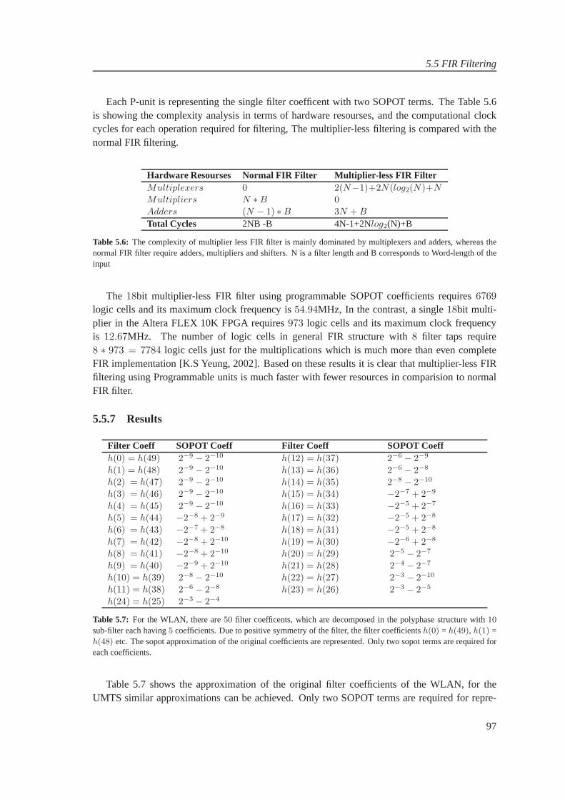
5.5 FIR Filtering
Each P-unit is representing the single filter coefficent withtwo SOPOT terms. The Table 5.6is showing the complexity analysis in terms of hardware resourses, and the computational clockcycles for each operation required for filtering, The multiplier-less filtering is compared with thenormal FIR filtering.
Hardware Resourses Normal FIR Filter Multiplier-less FIR FilterMultiplexers 0 2(N−1)+2N(log2(N)+N
Multipliers N ∗ B 0
Adders (N − 1) ∗ B 3N + B
Total Cycles 2NB -B 4N-1+2Nlog2(N)+B
Table 5.6: The complexity of multiplier less FIR filter is mainly dominated by multiplexers and adders, whereas thenormal FIR filter require adders, multipliers and shifters.N is a filter length and B corresponds to Word-length of theinput
The 18bit multiplier-less FIR filter using programmable SOPOT coefficients requires6769logic cells and its maximum clock frequency is54.94MHz, In the contrast, a single18bit multi-plier in the Altera FLEX 10K FPGA requires973 logic cells and its maximum clock frequencyis 12.67MHz. The number of logic cells in general FIR structure with8 filter taps require8 ∗ 973 = 7784 logic cells just for the multiplications which is much more than even completeFIR implementation [K.S Yeung, 2002]. Based on these results it is clear that multiplier-less FIRfiltering using Programmable units is much faster with fewerresources in comparision to normalFIR filter.
5.5.7 Results
Filter Coeff SOPOT Coeff Filter Coeff SOPOT Coeffh(0) = h(49) 2−9 − 2−10 h(12) = h(37) 2−6 − 2−9
h(1) = h(48) 2−9 − 2−10 h(13) = h(36) 2−6 − 2−8
h(2) = h(47) 2−9 − 2−10 h(14) = h(35) 2−8 − 2−10
h(3) = h(46) 2−9 − 2−10 h(15) = h(34) −2−7 + 2−9
h(4) = h(45) 2−9 − 2−10 h(16) = h(33) −2−5 + 2−7
h(5) = h(44) −2−8 + 2−9 h(17) = h(32) −2−5 + 2−8
h(6) = h(43) −2−7 + 2−8 h(18) = h(31) −2−5 + 2−8
h(7) = h(42) −2−8 + 2−10 h(19) = h(30) −2−6 + 2−8
h(8) = h(41) −2−8 + 2−10 h(20) = h(29) 2−5 − 2−7
h(9) = h(40) −2−9 + 2−10 h(21) = h(28) 2−4 − 2−7
h(10) = h(39) 2−8 − 2−10 h(22) = h(27) 2−3 − 2−10
h(11) = h(38) 2−6 − 2−8 h(23) = h(26) 2−3 − 2−5
h(24) = h(25) 2−3 − 2−4
Table 5.7: For the WLAN, there are50 filter coefficents, which are decomposed in the polyphase structure with10
sub-filter each having5 coefficients. Due to positive symmetry of the filter, the filter coefficientsh(0) = h(49), h(1) =h(48) etc. The sopot approximation of the original coefficients are represented. Only two sopot terms are required foreach coefficients.
Table 5.7 shows the approximation of the original filter coefficients of the WLAN, for theUMTS similar approximations can be achieved. Only two SOPOTterms are required for repre-
97

Chapter 5 Implementation Analysis
senting each filter coefficient. Maximum power of2 is 10 which means that we only require10right shifts in order to achieve the FIR filtering, whereas the normal filtering requires shifts equalto the word-length. The Figure 5.35 shows the impulse reponse of the approximated coefficientsin order to represent it in power of two. The approximated impulse response is very similar tothe original impulse response which is shown in the simulation chapter (WLAN) and therefore thepolyphase channelizer output is also acceptable with required accuracy as shown in Figure 5.36.
0 10 20 30 40 50−0.05
0
0.05
0.1
0.15
0.2Approximated Impulse Response(SOPOT)
Filter Lenght N
Filt
er C
oeffi
cien
ts
Figure 5.35: The approximated impulse response of the polyphase filter ofWLAN. The approximation in SOPOT formis shown in 5.7.
−1 −0.5 0 0.5 1
x 107
−80
−70
−60
−50
−40
−30
−20
−10
0Output signal Spectrum CH−2
Frequency
dB
Figure 5.36: The output of the polyphase channelizer for the second channel of the WLAN. The results shows that theapproximations are acceptable
There are25 P-Units require for implementing the WLAN polyphase filter,which can be ob-tained by cascading the two structures shown in Figure 5.33 as each structure implments16 coef-ficients.
98

5.6 Cost Function for the Implementation
The multiplier-less FIR filtering technique described in this section could possible be optimizedin the VLSI design. Most of the operations can be hardwired and highly optimized based on thegiven cost function (Area, Time, Power, etc.)
5.6 Cost Function for the Implementation
When making a decision, leading to an outcome, there are someparameters involved in the design.The suitable architecture can be analysed and decided basedon the parameters, such as algorithm,constraint and platform in the following manner:
Architecture(i) = fAlgorithm(i), Constraints(i), P latform(i)
It means that the intrinsic property of the algorithm, the constraints and the final target platform canhave a strong influence on final architecture decision. This means that the final architecture shouldinherit the intrinsic properties of the algorithm. The parameters for choosing the final architecturecan be described by the cost function based on the common design metrics in the following way:
C = fTE,A,N, TD
• Execution time (TE): The execution time is the time needed toexecute the algorithm, whichcorresponds to the performance in the design metrics. Mainly the data length determine theexecution time, i.e., longer data length results in longer execution time, as longer arithmeticoperations are to be performed.
• Area (A): Area is defined as the amount of hardware used in the system. It relates to thephysical size of the product and has the influence on the powerconsumption and the finan-cial cost. Applied technology and the data length determines the area.
• Numerical properties (N): Rounding noise is produced when data are rounded to finite datalength. Applied data length determines the amount of the rounding noise. i.e., longer datalength causes less noise. Rounding noise can cause degradation in algorithm performancein comparison. Algorithms sensitive to rounding noise may become unstable in the worstcase.
• Development time (TD): Development time is defined as the time needed to design andimplement the algorithm on to the simulation or hardware platform.
The purpose of cost function is to optimize the required variable/variables with respect to someconstraints. In this project, the focus is on the area optimization of the algorithm with respect tothe time constraints (105MHz for UMTS and 120MHz for WALN). The area is bounded by thearea parameter of Xilinx Virtex-IV XC4VSX35 chip.
5.7 Design Space Exploration
A design can be implemented in a number of ways on a number of architectures. These numberof solutions form a huge solution space. Design space exploration provides area-time trade offcurves of the implementation of a design. This is due to inherent parallelism that can be deployed
99
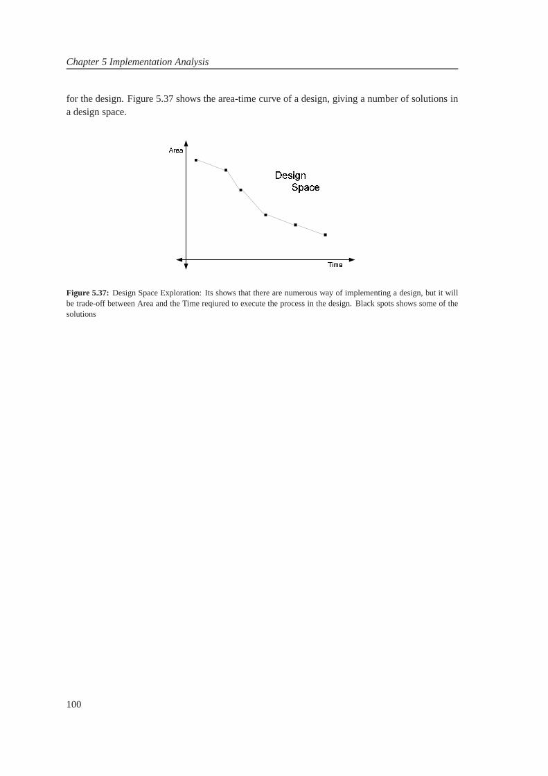
Chapter 5 Implementation Analysis
for the design. Figure 5.37 shows the area-time curve of a design, giving a number of solutions ina design space.
Figure 5.37: Design Space Exploration: Its shows that there are numerousway of implementing a design, but it willbe trade-off between Area and the Time reqiured to execute the process in the design. Black spots shows some of thesolutions
100
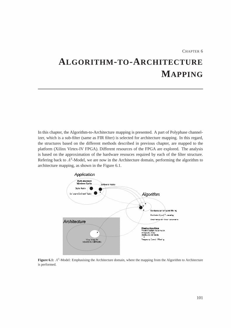
CHAPTER 6
ALGORITHM -TO-ARCHITECTURE
M APPING
In this chapter, the Algorithm-to-Architecture mapping ispresented. A part of Polyphase channel-izer, which is a sub-filter (same as FIR filter) is selected forarchitecture mapping. In this regard,the structures based on the different methods described in previous chapter, are mapped to theplatform (Xilinx Virtex-IV FPGA). Different resources of the FPGA are explored. The analysisis based on the approximation of the hardware resouces required by each of the filter structure.Refering back toA3-Model, we are now in the Architecture domain, performing the algorithm toarchitecture mapping, as shown in the Figure 6.1.
! " # $ $ % $ & ' ( ) ( * +)' ,-)"' ./*0122334,
5678 9:;8<=><?>@ 9?A 7A;; B<> 9C DEFGH IJK LIM NEDEFGH IJK OKFNPKM LIM NEQRSTUVRWX Y SXZ VRT [\ ]# ! *^$$!! *_ $ ^ _ `! ^ a $22^2 b!$_ 2
Figure 6.1: A3-Model: Emphasising the Architecture domain, where the mapping from the Algorithm to Architectureis performed.
101

Chapter 6 Algorithm-to-Architecture Mapping
In the polyphase channelizers, UMTS polyphase filter bank has 21 sub-filters each of length 12taps, whereas WLAN polyphase filter bank has 5 sub-filters each of length 10 taps. So we have todesign filters of length 12 and 10. The basic design parameters are:
• Input Data-width: 16 Bits
• Filter’s Coefficient Data-width: 18 Bits
• Input data and Filter Coefficent both are taken as Real data (for simplicity)
A filter length of 16 is selected to make the flow simpler. The design is based on followingrequirements:
• Clock frequency for WLAN sub-filters is 120MHz and for UMTS sub-filters is 105MHz
• In the serial implementation of the Polyphase filter bank (asdiscussed in the previous chap-ter), it is required to have a swapable coefficient memory bank, so that one subfilter’s coeffi-cients are used in multiply-accumulate process while the next coefficients are being loadedinto the other memory bank for the next process.
6.1 Parallel Multipliers and Accumulators
In the custom VLSI chip, each multiplier was re-used eight times per input sample. This meantthat each tap would compute eight products and accumulate them together every input sample foreight separate coefficients. In this manner, 2 MACs were all that were needed to compute a 16-tapfilter. However, each MAC needed to operate at a clock rate eight times that of the input data rate,so for a 105MHz input sample rate for UMTS, a 840 MHz clock was required, and for a 120MHzinput sample rate for WLAN, a 960MHz clock was required. These clock specifications are quitehigh for Vixtex-FPGA (Maximum clock freq. of 500MHz). The clock speed can be decreasedby decreasing the number of taps per MAC to be processed. By processing 4 taps per MAC, therequired clock speed becomes 420MHz for UMTS and 480MHz for WLAN, which are within thespecifications of Vixtex-FPGA, but it will increase the number of MACs.
The Xilinx Virtex series FPGA has dedicated multiplicationresources so that two multiplica-tion bits can fit into a single slice. Ana-bit by b-bit parallel multiplier requires approximately
b log2b + (b − 1)a2
(6.1)
CLB slices [Xilinx_Multiplier, 2000] [Moeller, 1999]. A 16-bit by 18-bit parallel multiplierwould require 163 slices. Therefore, the multipliers alonein a parallel MAC structure of 4 tapsper MAC would require 652 slices. The adders, additional registers and control logic requiredfor this design would push this number higher. A 16-Tap parallel MAC filter is shown in Fig-ure 6.2 [Moeller, 1999].
If each MAC was responsible for 4 taps, the coefficient storage for a single bank for a singleMAC would require 9 slices since a slice contains two 16x1 RAMblocks, and one RAM blockcould hold a single bit for all 4 taps (maximum 16 taps). 18-bit coefficients would therefore require
102
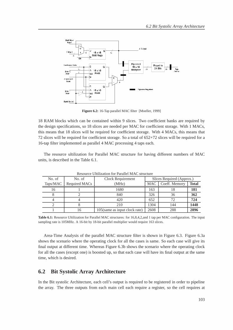
6.2 Bit Systolic Array Architecture
! ! "# $# % %%&' () *+ ,, -&' () .+ ,, -&'() /0 10 23450 667270 (385 ',450 667270 (3 9' 3' 4 1) %: ;(<=3/3' -3 >0?;(<=3 : @=3 <=3 A' <@=3<=3BCBC
% D 7<0 17(0 E0 F 7G30 -GFigure 6.2: 16-Tap parallel MAC filter [Moeller, 1999]
18 RAM blocks which can be contained within 9 slices. Two coefficient banks are required bythe design specifications, so 18 slices are needed per MAC forcoefficient storage. With 1 MACs,this means that 18 slices will be required for coefficient storage. With 4 MACs, this means that72 slices will be required for coefficient storage. So a totalof 652+72 slices will be required for a16-tap filter implemented as parallel 4 MAC processing 4 tapseach.
The resource ultilization for Parallel MAC structure for having different numbers of MACunits, is described in the Table 6.1.
Resource Ultilization for Parallel MAC structureNo. of No. of Clock Requirement Slices Required (Approx.)
Taps/MAC Required MACs (MHz) MAC Coeff. Memory Total
16 1 1680 163 18 1818 2 840 326 36 3624 4 420 652 72 7242 8 210 1304 144 14481 16 105(same as input clock rate)2608 288 2896
Table 6.1: Resource Ultilization for Parallel MAC structures: for 16,8,4,2,and 1 tap per MAC configuration. The inputsampling rate is 105MHz. A 16-bit by 18-bit parallel multiplier would require 163 slices.
Area-Time Analysis of the parallel MAC structure filter is shown in Figure 6.3. Figure 6.3ashows the scenario where the operating clock for all the cases is same. So each case will give itsfinal output at different time. Whereas Figure 6.3b shows thescenario where the operating clockfor all the cases (except one) is boosted up, so that each casewill have its final output at the sametime, which is desired.
6.2 Bit Systolic Array Architecture
In the Bit systolic Architecture, each cell’s output is required to be registered in order to pipelinethe array. The three outputs from each main cell each requirea register, so the cell requires at
103

Chapter 6 Algorithm-to-Architecture Mapping
Area-Time Analysis
2896
1448
724
362181
0
500
1000
1500
2000
2500
3000
3500
0 0.2 0.4 0.6 0.8 1 1.2
Time (x 9.52nsec)
Are
a (S
lices
)
! " # $ % ! ! & $ ! ' # # ( ) * + , - # ! " # $ % ! ! & ! . ! $ ! '/ $ ! $ 0 1 . / $ ( ) * + , - 2 $ $ / & $ ! ! & ( ) * + ,' - ' 3 -Area-Time Analysis
2896
1448
724
362181
0
500
1000
1500
2000
2500
3000
3500
0 1 2 3 4 5 6Time (x 9.52nsec)
Are
a (S
lices
)
Figure 6.3: Area-Time Analysis of the parallel MAC structure filter. Figure 6.3a shows the scenario where the operatingclock for all the cases is same. So each case will give its finaloutput at different time. Whereas Figure 6.3b showsthe scenario where the operating clock for all the cases (except one) is boosted up, so that each case will have its finaloutput at the same time, which is desired.
least one and a half slices. Each main cell also must compute two functions of four inputs (each ofwhich can fit into a Virtex LUT) and needs to store one bit of a coefficient (without dualbankingas required by the design specifications). A CLB LUT may be used to store this bit. Therefore,each main cell requires three registers and three LUTs. Two main cells may be contained withinthree slices, which would contain six LUTs and six registers, without dual-banking.
According to [Chin-Liang Wang and Chen, 1988], the number ofmain cells required for thesystolic array is(B + L).N , where B = the number of bits in the input, N = the number of taps,andL = log2N . For a 16-tap, 18-bit filter, the number of main cells required for the systolic arrayis 320. This would require 480 slices to implement. Since this structure is bit-level pipelined, oneoutput is produced every B clock cycles, or every 16 clock cycles for the 16-bit design. Therefore,for a 105 MHz input and output sample rate, the array will haveto operate at 1680MHz, whichis too high for Vixtex-FPGA (Maximum clock freq. of 500MHz).In addition to the main array,there are other cells required for the design that would alsoincrease the area.
This architecture was used for a full-custom, transistor mask-level design. The reason that thisdesign was so efficient for a full-custom chip versus a FPGA isthat it requires a very fine-grainedarchitecture. The basic cell in the bit-level systolic array is only three registers and a few logicgates, which takes up very little area on a custom chip. However, for a coarse-grained FPGA suchas the Virtex, the simplicity of a single cell is actually a drawback, area-wise. A better approachfor a FPGA design is to use cell sizes that more appropriatelymap into the FPGA’s architecture,such as those used in Distributed Arithmetic.
6.2.1 Distributed Arithmetic
The distributed arithmetic approach can easily be expandedto 16-taps, but two problems remain.First of all, the DA coefficients are constant, but the designrequirements demand two swapable,
104
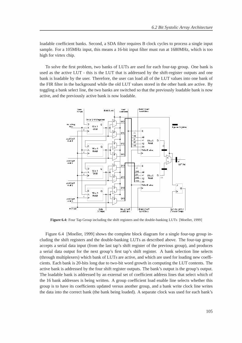
6.2 Bit Systolic Array Architecture
loadable coefficient banks. Second, a SDA filter requires B clock cycles to process a single inputsample. For a 105MHz input, this means a 16-bit input filter must run at 1680MHz, which is toohigh for virtex chip.
To solve the first problem, two banks of LUTs are used for each four-tap group. One bank isused as the active LUT - this is the LUT that is addressed by theshift-register outputs and onebank is loadable by the user. Therefore, the user can load allof the LUT values into one bank ofthe FIR filter in the background while the old LUT values stored in the other bank are active. Bytoggling a bank select line, the two banks are switched so that the previously loadable bank is nowactive, and the previously active bank is now loadable.
!"#$% & '('( !"#$% & '('( !"#$% & '('( !"#$% & '('(
!"#$'% &$($)$*+,-./ 01234/ !"#$'% &$($)$*+,-./ 01234/
($'($ (($)($*)$')$()$))$*
($'($(($)($*)$')$()$))$* '(
5555
6
7 8 9: ;
#% & ; < = >/,-24 >?-@. A/B-C./,C
7DE FG 8HIE 7
Figure 6.4: Four Tap Group including the shift registers and the double-banking LUTs [Moeller, 1999]
Figure 6.4 [Moeller, 1999] shows the complete block diagramfor a single four-tap group in-cluding the shift registers and the double-banking LUTs as described above. The four-tap groupaccepts a serial data input (from the last tap’s shift register of the previous group), and producesa serial data output for the next group’s first tap’s shift register. A bank selection line selects(through multiplexers) which bank of LUTs are active, and which are used for loading new coeffi-cients. Each bank is 20-bits long due to two-bit word growth in computing the LUT contents. Theactive bank is addressed by the four shift register outputs.The bank’s output is the group’s output.The loadable bank is addressed by an external set of coefficient address lines that select which ofthe 16 bank addresses is being written. A group coefficient load enable line selects whether thisgroup is to have its coefficients updated versus another group, and a bank write clock line writesthe data into the correct bank (the bank being loaded). A separate clock was used for each bank’s
105
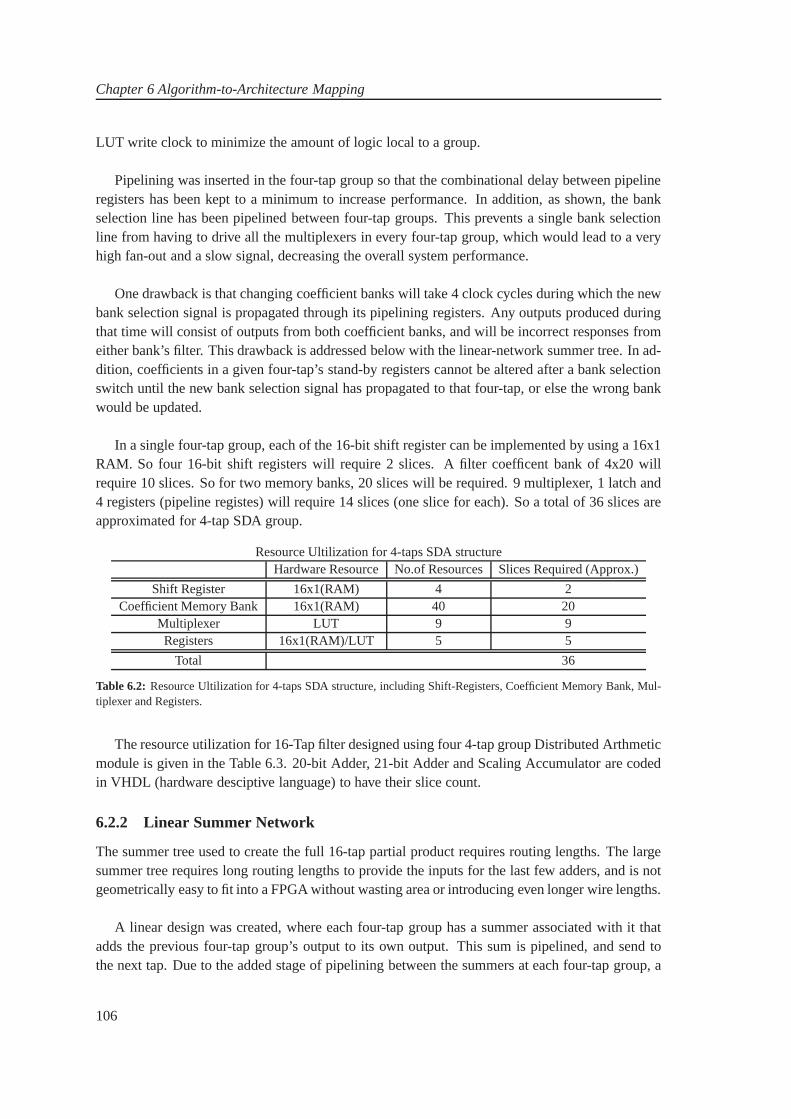
Chapter 6 Algorithm-to-Architecture Mapping
LUT write clock to minimize the amount of logic local to a group.
Pipelining was inserted in the four-tap group so that the combinational delay between pipelineregisters has been kept to a minimum to increase performance. In addition, as shown, the bankselection line has been pipelined between four-tap groups.This prevents a single bank selectionline from having to drive all the multiplexers in every four-tap group, which would lead to a veryhigh fan-out and a slow signal, decreasing the overall system performance.
One drawback is that changing coefficient banks will take 4 clock cycles during which the newbank selection signal is propagated through its pipeliningregisters. Any outputs produced duringthat time will consist of outputs from both coefficient banks, and will be incorrect responses fromeither bank’s filter. This drawback is addressed below with the linear-network summer tree. In ad-dition, coefficients in a given four-tap’s stand-by registers cannot be altered after a bank selectionswitch until the new bank selection signal has propagated tothat four-tap, or else the wrong bankwould be updated.
In a single four-tap group, each of the 16-bit shift registercan be implemented by using a 16x1RAM. So four 16-bit shift registers will require 2 slices. A filter coefficent bank of 4x20 willrequire 10 slices. So for two memory banks, 20 slices will be required. 9 multiplexer, 1 latch and4 registers (pipeline registes) will require 14 slices (oneslice for each). So a total of 36 slices areapproximated for 4-tap SDA group.
Resource Ultilization for 4-taps SDA structureHardware Resource No.of Resources Slices Required (Approx.)
Shift Register 16x1(RAM) 4 2Coefficient Memory Bank 16x1(RAM) 40 20
Multiplexer LUT 9 9Registers 16x1(RAM)/LUT 5 5
Total 36
Table 6.2: Resource Ultilization for 4-taps SDA structure, includingShift-Registers, Coefficient Memory Bank, Mul-tiplexer and Registers.
The resource utilization for 16-Tap filter designed using four 4-tap group Distributed Arthmeticmodule is given in the Table 6.3. 20-bit Adder, 21-bit Adder and Scaling Accumulator are codedin VHDL (hardware desciptive language) to have their slice count.
6.2.2 Linear Summer Network
The summer tree used to create the full 16-tap partial product requires routing lengths. The largesummer tree requires long routing lengths to provide the inputs for the last few adders, and is notgeometrically easy to fit into a FPGA without wasting area or introducing even longer wire lengths.
A linear design was created, where each four-tap group has a summer associated with it thatadds the previous four-tap group’s output to its own output.This sum is pipelined, and send tothe next tap. Due to the added stage of pipelining between thesummers at each four-tap group, a
106
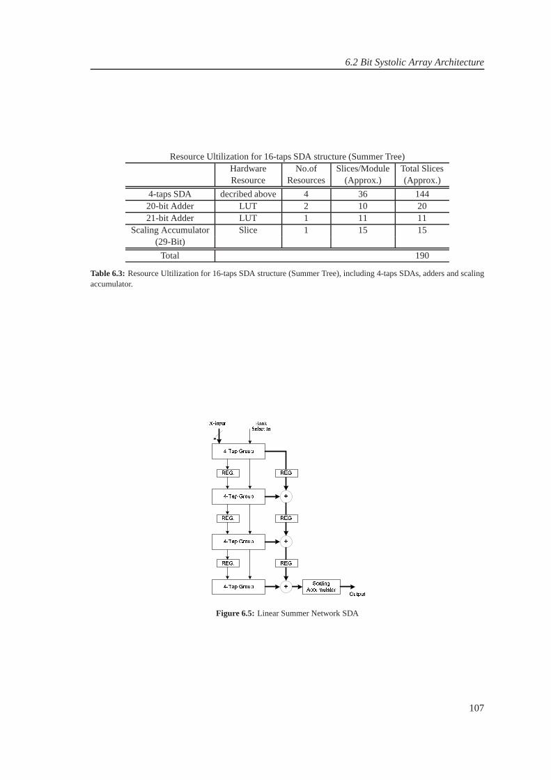
6.2 Bit Systolic Array Architecture
Resource Ultilization for 16-taps SDA structure (Summer Tree)Hardware No.of Slices/Module Total SlicesResource Resources (Approx.) (Approx.)
4-taps SDA decribed above 4 36 14420-bit Adder LUT 2 10 2021-bit Adder LUT 1 11 11
Scaling Accumulator Slice 1 15 15(29-Bit)
Total 190
Table 6.3: Resource Ultilization for 16-taps SDA structure (Summer Tree), including 4-taps SDAs, adders and scalingaccumulator.
!"#$#% &
Figure 6.5: Linear Summer Network SDA
107
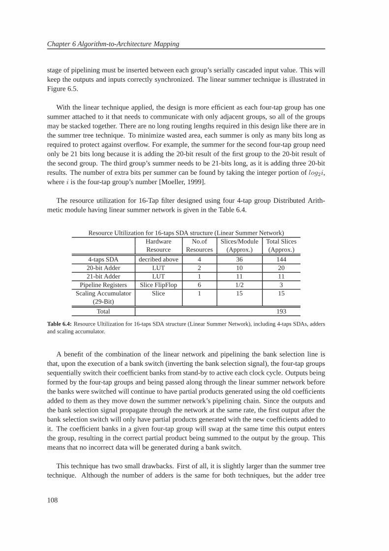
Chapter 6 Algorithm-to-Architecture Mapping
stage of pipelining must be inserted between each group’s serially cascaded input value. This willkeep the outputs and inputs correctly synchronized. The linear summer technique is illustrated inFigure 6.5.
With the linear technique applied, the design is more efficient as each four-tap group has onesummer attached to it that needs to communicate with only adjacent groups, so all of the groupsmay be stacked together. There are no long routing lengths required in this design like there are inthe summer tree technique. To minimize wasted area, each summer is only as many bits long asrequired to protect against overflow. For example, the summer for the second four-tap group needonly be 21 bits long because it is adding the 20-bit result of the first group to the 20-bit result ofthe second group. The third group’s summer needs to be 21-bits long, as it is adding three 20-bitresults. The number of extra bits per summer can be found by taking the integer portion oflog2i,wherei is the four-tap group’s number [Moeller, 1999].
The resource utilization for 16-Tap filter designed using four 4-tap group Distributed Arith-metic module having linear summer network is given in the Table 6.4.
Resource Ultilization for 16-taps SDA structure (Linear Summer Network)Hardware No.of Slices/Module Total SlicesResource Resources (Approx.) (Approx.)
4-taps SDA decribed above 4 36 14420-bit Adder LUT 2 10 2021-bit Adder LUT 1 11 11
Pipeline Registers Slice FlipFlop 6 1/2 3Scaling Accumulator Slice 1 15 15
(29-Bit)
Total 193
Table 6.4: Resource Ultilization for 16-taps SDA structure (Linear Summer Network), including 4-taps SDAs, addersand scaling accumulator.
A benefit of the combination of the linear network and pipelining the bank selection line isthat, upon the execution of a bank switch (inverting the bankselection signal), the four-tap groupssequentially switch their coefficient banks from stand-by to active each clock cycle. Outputs beingformed by the four-tap groups and being passed along throughthe linear summer network beforethe banks were switched will continue to have partial products generated using the old coefficientsadded to them as they move down the summer network’s pipelining chain. Since the outputs andthe bank selection signal propagate through the network at the same rate, the first output after thebank selection switch will only have partial products generated with the new coefficients added toit. The coefficient banks in a given four-tap group will swap at the same time this output entersthe group, resulting in the correct partial product being summed to the output by the group. Thismeans that no incorrect data will be generated during a bank switch.
This technique has two small drawbacks. First of all, it is slightly larger than the summer treetechnique. Although the number of adders is the same for bothtechniques, but the adder tree
108
6.3 Fast FIR Algorithm
requires less area as the adder bit size grows, whereas the linear network requires more. However,as long as the design still fits within a Virtex device, this isacceptable. The second drawback isthat the output has a latency of 4 clock cycles due to the pipelining of each four-tap group’s output.In most signal processing applications, small latencies such as this are not detrimental.
6.2.3 Achieving Low clock rate performance for 105 MHz Sample-Rate
The serial distributed arithmetic design as described above requires a clock rate 16 times fasterthan the input data rate. For a 105 MHz data rate, this means the serial filters must run at 1680MHz.
Two solutions exist to solve this problem. The first is to operate the SDA filter at 1680 MHz,using the Virtex DLL to multiply the external 105 MHz clock upto a 1680 MHz internal clockrate. But the DLL can work up to 500 MHz. The second is to use 2-bit PDA, with two 16-tapSDA filters. A clock rate 8 times faster than the sample rate would be required for this design, andthe internal filters would have to operate at 840 MHz, yet the design would require twice as mucharea as a SDA design. Even this solution donot fit for the clockspecification of the Virtex Chip.To use 4-bit PDA, with four 16-tap SDA filters, would requiresa clock rate 4 times faster than thesample rate. The internal filters would have to operate at 420MHz, but the design would requirefour times the area as a SDA design. The trade-off between thethese techniques is speed versusarea. The 4-bit PDA design requires 768 slices for the 16-taplinear-network filter.
The Area-Time analysis for Distributed Arithmetic technique, having different numbers of bitsprocessed at a time is shown in Figure 6.6. Figure 6.6a shows the scenario where the operatingclock for all the cases is same. So each case will give its finaloutput at different time. WhereasFigure 6.3b shows the scenario where the operating clock forall the cases (except one at 105MHz)is boosted up, so that each case will have its final output at the same time, which is desired.
6.3 Fast FIR Algorithm
The parallel MAC approach to the filtering problem can be combined with the FFA algorithm toderive small filtering structures [Moeller, 1999]. In the parallel MAC approach implementation, 4MACs used to calculate a 16-tap FIR response by having each MAC performing four multiplica-tions per input word, so that each MAC handle four filter taps.This could be decreased to 2 tapsper MAC, so that 8 MACs would be needed with an 210 MHz clock rate.
If each MAC is responsible for 2 taps, 8 MACs would be required, but a 210MHz clock rateis required. The new FFA approach would take the polyphase decomposition of the filter. Eachpolyphase filter (i.e.H0 or H1) would be half the size of the original 16-tap filter, or 8-taps. Ap-plying the FFA algorithm would require three 8-tap filters. Each of these smaller filters would nowhave to run at only half the original filter’s sample rate, or 52.5 MHz to maintain an overall samplerate of 105 MHz (the FFA approach allows an overall throughput twice that of the individual fil-ters’ sample rates). Each polyphase filter could be implemented with 4 MACs, where each MAChandled 2 taps. The benefit is that the sample rate of each filter is now only 52.5 MHz, meaningthat each MAC would only have to run at 105 MHz to compute the results from 2 taps per input.
109

Chapter 6 Algorithm-to-Architecture Mapping
! " # $ # % & ' $ $ ( ) * + , - . $ ! " # $ # % & ' ' / $ " 0/ $ " # . # ( ) * + , - . 1 & # ( ) * + , -' . ' " . 2 2 2 3 Area-Time Analysis
3072
1536
768
384192
0
500
1000
1500
2000
2500
3000
3500
0 1 2 3 4 5 6Time (x 9.52nsec)
Are
a (S
lices
)
Area-Time Analysis
3072
1536
768
384192
0
500
1000
1500
2000
2500
3000
3500
0 0.2 0.4 0.6 0.8 1 1.2Time (x 9.52nsec)
Are
a (S
lices
) 4 2 2 4 3 2 ' . ' " .
Figure 6.6: The Area-Time analysis for Distributed Arithmetic technique, having different numbers of bits processedat a time. Figure 6.6a shows the scenario where the operatingclock for all the cases is same. So each case will giveits final output at different time. Whereas Figure 6.3b showsthe scenario where the operating clock for all the cases(except one at 105MHz) is boosted up, so that each case will have its final output at the same time, which is desired.
With no change in clock rate (i.e. at 210MHz), the total number of MACs would be decreased to6 (Polyphase structure) from the original 8.
One major change is that the middle filter would be multiplying 17-bit inputs by 19-bit coeffi-cients because of the one-bit word growth through the addition of before the filter and the one bitword growth in the addition of to compute the filter’s coefficients. Therefore, the middle polyphasefilter would be slightly larger than the other two filters. Theoverall FFA filter will also be slightlylarger due to the five extra summers and the delay element.
The middle filter requires MACs of size 17x19 bits, whereas the other two filters requiresMACs of size 16x18 bits. The area required by multipliers of size 17x19 bits and 16x18 bitsis 187 and 173 slices respectively. So 16 multipliers of 16x18 bits (both top and bottom filters)requires 2768 slices and 8 multipliers of 17x19 bits (middlefilter) requires 1496 slices, whichresults in overall slices of4264. The five extra adders will push this value little high.
6.4 Frequency Domain Filtering
For the frequency domain filtering implementation, a 32-point FFT and IFFT are required (previ-ous chapter). However, since the input data is real, both thereal and imaginary parts of the FFTmay be used to hold the real input data [Alan V. Oppenheim, 1999] [Groginsky and Works., ].Therefore, a 32-point FFT can be calculated with a 16-point FFT structure.
The next step for the frequency domain filtering implementation was to determine the bit-sizerequired for the FFTs in order to meet the custom VLSI chip’s output precision. The minimumbit-width to maintain approximately 18 bits of output precision was determined for each variable
110
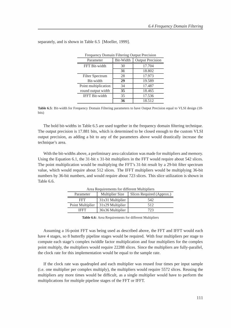
6.4 Frequency Domain Filtering
separately, and is shown in Table 6.5 [Moeller, 1999].
Frequency Domain Filtering Output PrecisionParameter Bit-Width Output Precision
FFT Bit-width 30 17.70431 18.802
Filter Spectrum 28 17.973Bit-width 29 19.589
Point multiplication 34 17.487round output width 35 18.465
IFFT Bit-width 35 17.53636 18.512
Table 6.5: Bit-width for Frequency Domain Filtering parameters to have Output Precision equal to VLSI design (18-bits)
The bold bit-widths in Table 6.5 are used together in the frequency domain filtering technique.The output precision is 17.881 bits, which is determined to be closed enough to the custom VLSIoutput precision, as adding a bit to any of the parameters above would drastically increase thetechnique’s area.
With the bit-widths above, a preliminary area calculation was made for multipliers and memory.Using the Equation 6.1, the 31-bit x 31-bit multipliers in the FFT would require about 542 slices.The point multiplication would be multiplying the FFT’s 31-bit result by a 29-bit filter spectrumvalue, which would require about 512 slices. The IFFT multipliers would be multiplying 36-bitnumbers by 36-bit numbers, and would require about 723 slices. This slice utilization is shown inTable 6.6.
Area Requirements for different MultipliersParameter Multiplier Size Slices Required (Approx.)
FFT 31x31 Multiplier 542Point Multiplier 31x29 Multiplier 512
IFFT 36x36 Multiplier 723
Table 6.6: Area Requirements for different Multipliers
Assuming a 16-point FFT was being used as described above, the FFT and IFFT would eachhave 4 stages, so 8 butterfly pipeline stages would be required. With four multipliers per stage tocompute each stage’s complex twiddle factor multiplication and four multipliers for the complexpoint multiply, the multipliers would require 22288 slices. Since the multipliers are fully-parallel,the clock rate for this implementation would be equal to the sample rate.
If the clock rate was quadrupled and each multiplier was reused four times per input sample(i.e. one multiplier per complex multiply), the multipliers would require 5572 slices. Reusing themultipliers any more times would be difficult, as a single multiplier would have to perform themultiplications for multiple pipeline stages of the FFT or IFFT.
111
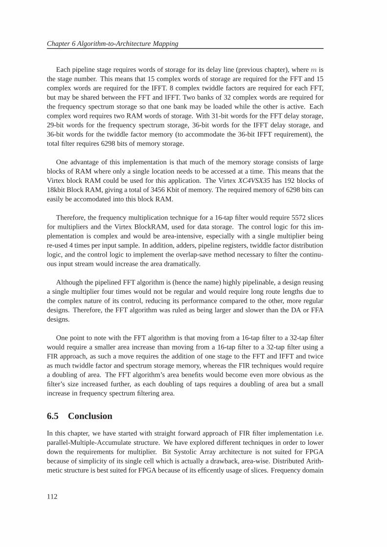
Chapter 6 Algorithm-to-Architecture Mapping
Each pipeline stage requires words of storage for its delay line (previous chapter), wherem isthe stage number. This means that 15 complex words of storageare required for the FFT and 15complex words are required for the IFFT. 8 complex twiddle factors are required for each FFT,but may be shared between the FFT and IFFT. Two banks of 32 complex words are required forthe frequency spectrum storage so that one bank may be loadedwhile the other is active. Eachcomplex word requires two RAM words of storage. With 31-bit words for the FFT delay storage,29-bit words for the frequency spectrum storage, 36-bit words for the IFFT delay storage, and36-bit words for the twiddle factor memory (to accommodate the 36-bit IFFT requirement), thetotal filter requires 6298 bits of memory storage.
One advantage of this implementation is that much of the memory storage consists of largeblocks of RAM where only a single location needs to be accessed at a time. This means that theVirtex block RAM could be used for this application. The Virtex XC4VSX35has 192 blocks of18kbit Block RAM, giving a total of 3456 Kbit of memory. The required memory of 6298 bits caneasily be accomodated into this block RAM.
Therefore, the frequency multiplication technique for a 16-tap filter would require 5572 slicesfor multipliers and the Virtex BlockRAM, used for data storage. The control logic for this im-plementation is complex and would be area-intensive, especially with a single multiplier beingre-used 4 times per input sample. In addition, adders, pipeline registers, twiddle factor distributionlogic, and the control logic to implement the overlap-save method necessary to filter the continu-ous input stream would increase the area dramatically.
Although the pipelined FFT algorithm is (hence the name) highly pipelinable, a design reusinga single multiplier four times would not be regular and wouldrequire long route lengths due tothe complex nature of its control, reducing its performancecompared to the other, more regulardesigns. Therefore, the FFT algorithm was ruled as being larger and slower than the DA or FFAdesigns.
One point to note with the FFT algorithm is that moving from a 16-tap filter to a 32-tap filterwould require a smaller area increase than moving from a 16-tap filter to a 32-tap filter using aFIR approach, as such a move requires the addition of one stage to the FFT and IFFT and twiceas much twiddle factor and spectrum storage memory, whereasthe FIR techniques would requirea doubling of area. The FFT algorithm’s area benefits would become even more obvious as thefilter’s size increased further, as each doubling of taps requires a doubling of area but a smallincrease in frequency spectrum filtering area.
6.5 Conclusion
In this chapter, we have started with straight forward approach of FIR filter implementation i.e.parallel-Multiple-Accumulate structure. We have explored different techniques in order to lowerdown the requirements for multiplier. Bit Systolic Array architecture is not suited for FPGAbecause of simplicity of its single cell which is actually a drawback, area-wise. Distributed Arith-metic structure is best suited for FPGA because of its efficently usage of slices. Frequency domain
112

6.5 Conclusion
filtering is the most resource consuming. The FFT algorithm’s area benefits would become obvi-ous as the filter’s size increased, as each doubling of taps requires a doubling of area but a smallincrease in frequency spectrum filtering area.
So finally Distributed Arithmetic structure is delected forthe final implementation to the FPGAbecause of being resource efficent. Area-time analysis of these different structured filters is shownin Figure 6.7.
Area-Time Analysis
0
1000
2000
3000
4000
5000
6000
0 0.5 1 1.5
Time (x 9.52nsec)
Are
a (S
lices
)
Area (Parallel-MAC)
Area (DA)
Area (FFA)
Area (Freq. DomainFiltering)
Figure 6.7: Area-Time Analysis of different structured filters
In this all analysis, we have not consider the parameter of maximum operating speed for thedesigns, which will definately restrict some of the design for the application. This is due to thefact that combinational logic lower down the maximum operating speed for a designed system.
The DSP48 slice is a new element in the Xilinx development model referred to as Applica-tion Specific Modular Blocks (ASMBL) architecture. The purpose of this model is to deliveroff-the-shelf programmable devices with the best mix of logic, memory, I/O, processors, clockmanagement, and digital signal processing. ASMBL is an efficient FPGA development model fordelivering off-the-shelf, flexible solutions ideally suited to different application domains.
Each XtremeDSP tile contains two DSP48 slices to form the basis of a versatile coarse-grainDSP architecture. Many DSP designs follow a multiply with addition. In Virtex-4 devices,these elements are supported in dedicated circuits. The DSP48 slices support many independentfunctions, including multiplier, multiplier-accumulator (MACC), multiplier followed by an adder,three-input adder, barrel shifter, wide bus multiplexers,magnitude comparator, or wide counter.The architecture also supports connecting multiple DSP48 slices to form wide math functions,DSP filters, and complex arithmetic without the use of general FPGA fabric.
The math portion of the DSP48 slice consists of an 18-bit x 18-bit, two’s complement mul-tiplier followed by three 48-bit datapath multiplexers (with outputs X, Y, and Z) followed by a
113
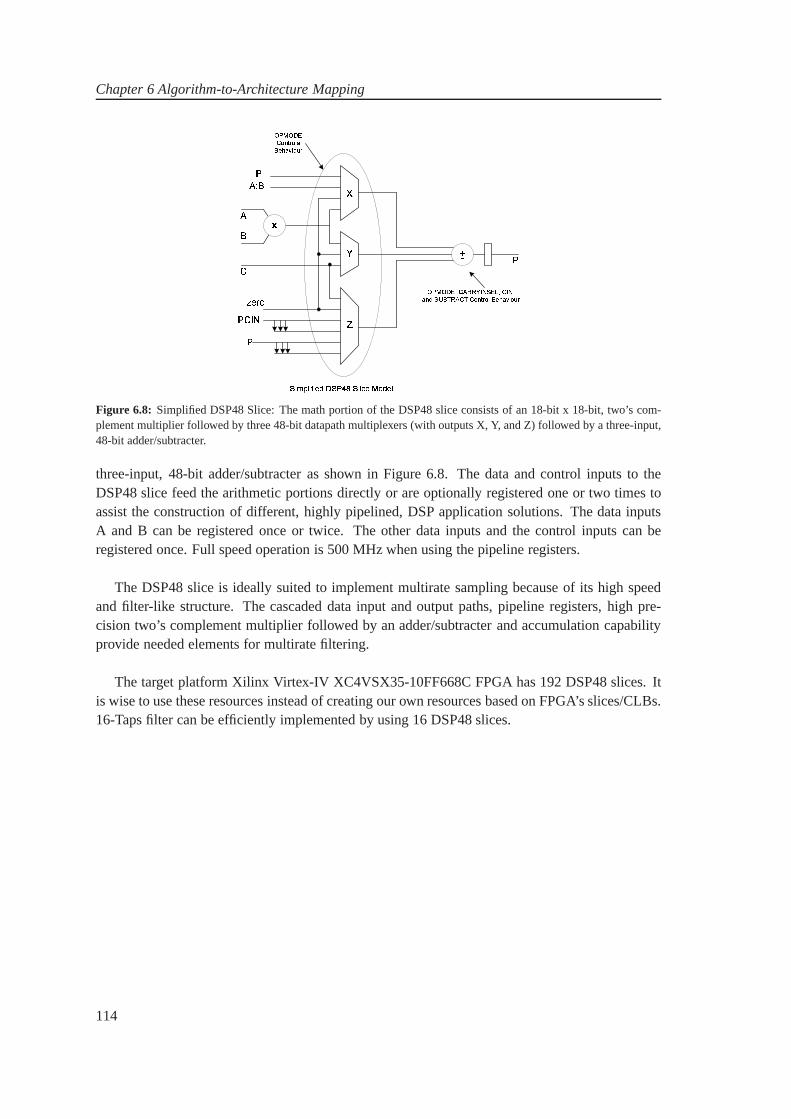
Chapter 6 Algorithm-to-Architecture Mapping
! "#$ $ % & '% ( #) *+ ,% - '
% & '% (.#)*+ ,% -'
/ 012304056 7/89: / 30;5 <=653Figure 6.8: Simplified DSP48 Slice: The math portion of the DSP48 slice consists of an 18-bit x 18-bit, two’s com-plement multiplier followed by three 48-bit datapath multiplexers (with outputs X, Y, and Z) followed by a three-input,48-bit adder/subtracter.
three-input, 48-bit adder/subtracter as shown in Figure 6.8. The data and control inputs to theDSP48 slice feed the arithmetic portions directly or are optionally registered one or two times toassist the construction of different, highly pipelined, DSP application solutions. The data inputsA and B can be registered once or twice. The other data inputs and the control inputs can beregistered once. Full speed operation is 500 MHz when using the pipeline registers.
The DSP48 slice is ideally suited to implement multirate sampling because of its high speedand filter-like structure. The cascaded data input and output paths, pipeline registers, high pre-cision two’s complement multiplier followed by an adder/subtracter and accumulation capabilityprovide needed elements for multirate filtering.
The target platform Xilinx Virtex-IV XC4VSX35-10FF668C FPGA has 192 DSP48 slices. Itis wise to use these resources instead of creating our own resources based on FPGA’s slices/CLBs.16-Taps filter can be efficiently implemented by using 16 DSP48 slices.
114
CHAPTER 7
CONCLUSION
7.1 Conclusions
The overall goal of this project is to design and implement a multi-standard software radio receiver.In a multi-standard secnario, WLAN and UMTS are taken as casestudy. The goal was stated inthe form of an initial problem:
How can an efficient multi-standard (WLAN & UMTS) software ra dioreceiver be designed and implemented.
In order to meet the goal, two project objectives were stated: 1) Select an algorithm / techniqueto obtain the desired functionality and 2) design and implement a system based on the selectedalgorithm. In the following, conclusions are made for theseobjectives.
In the selection of the technique for multi-standard software radio, bandpass sampling tech-nique has been selected. The UMTS and WLAN standards have 12 and 3 channels respectively,but only one channel from each standard is required at a time.It is required to down convertthese channels to baseband at the required sampling rate of 20MHz for WLAN and 61.44MHzfor UMTS. Initially, the combined band of UMTS and WLAN is undersampled at 676MHz. Thebandpass filters are requried to seperate these two bands of WLAN and UMTS. The applicationrequirement demands a linear phased characteristic of the bandpass filter, as the channels of eachstandard are very compactly spaced, and therefore the FIR filters are desirable choice. Further,a brief overview of the different methods which are used to calculate the filter coefficients arecompared. It is concluded that anOptimal Filter is required for the filtering purpose based on theapplication requirements. It is required to have that the minimum ripples in the passband whichis provided by the least square criterion in the optimal filter design. Finally, a channelizer wasrequired to obtain the desired functionality of downconversion and downsampling.
Two types of channelizer were considered in this case. The first one is the conventional chan-nelizer which has a downconverter followed by a lowpass filter, and rate converters. In this ap-proach, each channelizer works only for one of the channels.Thus to have multiple channels at theoutput, multiple channelizers are required. The second type is the polyphase channelizer which
115
Chapter 7 Conclusion
has commutator, polyphase partitioned filter and beam former by coherent phase summation. Ithas unique features of having all the channels at baseband with required sampling rate just byusing one filter (polyphase filter). It also has the features of efficient utilization of the resourcewith reduced clock-rate requirements. All the process to have a polyphase channelizer from theconventional channelizer is investigated. It uses theEquivalence TheoremandNobel Identity.The polyphase channelizer has been selected based on these unique features.
In order to meet the requirements of polyphase channelizer i.e. equal channel spacing and in-teger number of channels over the span of sampling frequency, we have gone through differentiterations. Different sampling frequencies are tried to have non-overlap alaised channels alongwith polyphase channelizer requirements of equal channel spacing and integer number of chan-nels. The sampling frequency is iteratively changed to 840 MHz, but still not perfectly matchedto one of the polyphase requirement of equal channel spacing. Unequal channel spacing results inbaseband offset for the downconverted signals.
In order to compensate for the baseband offset, we use a variant of polyphase channelizerthat has hyterdyning embedded in it. This variant polyphasechannelizer is best for the offsetsof multiples of quarter of channel spacing. Because of different channel bandwidth and channelspacing, both WLAN and UMTS require seperate polyphase channelizer. The resultant channel-izers for WLAN and UMTS have 35 and 168 sub-filters respectively with the input sampling rateof 840MHz. The processing load on sub-filters in the polyphase channelizer is reduced by lower-ing the input sampling frequency (as low as possible) by resampling the signal. In this case, theinput to bandpass filters in WLAN and UMTS path is considered as complex while making thefilter coefficients as real, which means that the output of thebandpass filter is complex with lesscomplexity i.e. multiplications and additions. This allowthe ssampling frequency for WLAN andUMTS to be lowered to 120 and 105 MHz respectively, due to having no interference with imagesignals. The resultant channelizers for WLAN and UMTS now have 5 and 21 sub-filters, with theinput sampling rate of 120 and 105MHz respectively.
In order to achieve the desired sampling rate at the output, different techniques are considered(such as) P/Q resampling and resampling embedded in the polyphase channelizer. Out of them,resampling embedded in the polyphase structure is selected. This is based on serpentine shift atthe input data and circular shifting the date before the coherent phase summation. The techniqueis further modified to have sliding movement of commutator and circulating the filter coefficient.
In the simulations, the results are the same having a band-select filter (complete spectrum) fol-lowed by bandpass filter UMTS and WLAN) as only having bandpass filters which removes theneed to select the complete band at the start. The signal power spectrum after passing through thebandpasss filter is still the same. The polyphase channelizers for WLAN and UMTS are simulatedto shows the desired signal at baseband with the required sampling rates of 20MHz and approx.61.44MHz respectively. The received signals have 50dB of dynamic range. The prototype filterfor WLAN has 50 taps which are partitioned into 5 polyphase branches, so that each sub-filter has10 coefficients. In UMTS channelizer, based on the required output sampling rate, a downfactorof approximately 17/10 is required, which has an upsamplingof 10. This upsampling factor of 10requires a 10 times longer prototype filter than the normal filter because of 10 times increase in
116

7.1 Conclusions
sampling frequency. The resultant prototype filter for UMTShas 2520 taps which are partitionedinto 210 polyphase branches, so that each sub-filter has 12 coefficients. Only one tenth (1/10)of the sub-filters i.e. 21 out of 210 are used at a time. This saves the processing panelty due toincreased filter length.
In the implementation phase, polyphase channelizers are analyzed in terms of the requiredcomponents, consisting of demultiplexer as commutator, a filter bank having polyphase filters, andfinally the coherent phase summation (multiply and accumulate). Different structural techniquesto carry out the implementation were presented. In this regard, general polyphase structure, op-timized structures - symmetric property based structure, adder shared structure, serial polyphasestructures with serial and parallel MAC are considered. Based on the complexity analysis, serialpolyphase structure with parallel MAC is selected for the final implementation.
In the individual sub-filter implemetation, different implementaion structures are considered.These being Parallel multipliers and accumulate, Bit systolic array, Distributed Arithmetic, FastFIR, frequency domain filtering and Multiplier less filtering techniques. Each structure and its vari-ants are analyzed in terms of hardware resources. The analysis is based on the approximations forthe area requirements for multipliers, adders and registers etc. For 16-tap filter Parallel-Multiplyand accumulate, Distributed Arithmetic, Fast FIR and Frequency domain filtering structures re-quire 2896(without adders), 3072, 4064, and 5572 slices, respectively. The Distributed arithmeticis found to be suitable for the implementation due to being resource efficient.
The focus of the above techniques is to use multipliers as less as possible, to save the area. Butdue to technology advancement, now the FPGAs have dedicatedmultiplier blocks which are moreefficient than the CLB-slices based multipliers in terms of operating speed and reduced powerrequirements. Xilinx FPGA, Virtex-IV has XtremeDSP blocksthat can perform multiplicationupto 500MHz rate. The system performance is increased by using these blocks. Each XtremeDSPblock has two DSP48 slices. So the polyphase filter bank implemented as serial-polyphase-filterstructure with parallel MAC for WLAN and UMTS channelizer can be built by using 10 and 12DSP48 slices respectively.
We have choosen the target architecture from the start, and we have said that it can only beFPGA or ASIC that can meet the required clock frequency for this project. We know from thestart that moderen FPGA’s like Virtex-IV have dedicated multipliers which are higly optimised asexplined above and at the end we are using them. But it was necessary to understand the knowl-edge of all the methods and techniques for the basic DSP operations and thats what we did. Nowat this stage we can say that the VLSI design is possible to have optimized architecture for DSPoperations based on the techniques that we have gone through. We can also guess that the tech-nique with Programmable SOPOT have an architecture which isvery similar to the architecture ofthe dedicated multipliers, (This is an assumption since theinternal architectures of the dedicatedmultipliers are confidentials of Xilinx, and they are not available).
The A3 model was used to describe the problems of mapping the algorithm to a system ar-chitecture. Many solutions of an architecture existed for the algorithm and the architecture alsohad to comply with the constraints of the application. The many different solutions formed a
117

Chapter 7 Conclusion
huge design space. Furthermore, the constraints on execution time and area consumption had tobe maintained making the mapping between the algorithm and the architecture an iterative process.
Finally, the answer to the initial problem is given:
Bandpass sampling technique has been selected for the WLAN and UMTSstandard receiver, which is followed by polyphase channelizers to have thechannels at the baseband with required sampling rates. Serial polyphase-channelizer implementation structure with parallel MAC is used for im-plementation. Polyphase sub-filter is implemented with Distributed Arith-metic structure or with Xilinx-DSP48 slices for improved performance.
In the following section, the future perspectives of the project are given. These perspectives arebased on the obtained results and considerations concerning the assumptions that have been made.
7.2 Future prospective
There is always room for improvement, and we also have some suggestions for the future work.
• In the project, we have considered a scenario by taking two standards (UMTS and WLAN),which can be expanded to include more standards.
• Polyphase channelizer is not used to its level best advantages of extracting all the channelsat the same time. This is due to the fact the different standards have different channelbandwidth and inter-carrier spacing. Even for one of the standards, all of its sub-channelsare not converted at the same time. This is due to the unequal channel spacing (from theDC). The polyphase channelizer can be used to its level best features that is extractingall of the channels for any standard, by having a heterodyning at the input of the polyphasechannelizer, and heterodyning-carrier is selected such that the translated channels have equalchannel spacing. This case will result in extracting all thechannels of a standard, justby using standard polyphase channelizer, not by its variantto compensate the offsets ofmultiples of quarter of channel spacing.
• In the polyphase channelizer for UMTS, the required downfactor of 875/512 is rounded to17/10, which results in the output sampling rate of 61.76 MHzinstead of 61.44 MHz. Arbi-trary sampling rate techique as mention in [Harris, 2006] can be used along with polyphasechannelizer to have the exact required sampling rate of 61.44 MHz.
• The implementation part is based on the analysis of the required hardware resources by hav-ing estimates and writing simple VHDL programs. The full implementation of the systemis a proposed future work.
118

BIBLIOGRAPHY
BIBLIOGRAPHY
[CSD, 2007] (2007).Stream radio goes digital.http://www.csdr.dk.
[A.G. Dempster, 1995] A.G. Dempster, M. M. (1995).Use of minimum adder and multiplier blocks in fir digital filter.IEEE Trans. circuit system II.
[Al-Haj, 2004] Al-Haj, A. M. (2004).An FPGA-Based Parallel Distributed Arithmetic Implementation of the 1-D Discrete Wavelet
Transform.Department of Computer Engineering, Princess Sumaya University for Technology, Al-Jubeiha
P.O.Box 1438, Amman 11941, Jordan. http://ai.ijs.si/informatica/PDF/29-2/13_Al-Haj-An%20FPGA-Based%20Parallel...pdf.
[Alan V. Oppenheim, 1999] Alan V. Oppenheim, R. W. S. (1999).Discrete-Time Signal Processing.Prentice Hall, second edition.
[Behjou Nastaran, 2006] Behjou Nastaran, Priyanto, B. E. J.O. K. L. T. (2006).Interference issues between umts & wlan in a multi-standardrf receiver.IST Mobile Wireless Comms Summit.
[Brannon, ] Brannon, B.Designing a Superheterodyne Receiver Using an IF Sampling Diversity Chipset,AN-502 AP-
PLICATION NOTE.http://www.analog.com.
[Chin-Liang Wang and Chen, 1988] Chin-Liang Wang, C.-H. W. and Chen, S.-H. (1988).Efficient bit-level systolic array implementation of fir andiir digital filters.IEEE Journal on Selected Areas in Communications, 6(3):484–493.
[Chris Dick, ] Chris Dick, f. h.Performing Simultaneous Arbitrary Spectral Translation and Sample Rate Change, in
Polyphase Interpolating or Decimating Filters in Transmitters and Receivers.www.xilinx.com/products/logicore/dsp/sdr_paper_1.pdf.
[Cook, 2006] Cook, P. G. (2006).
119

BIBLIOGRAPHY
Sdrf cognitive definition.http://www.sdrforum.org.
[Crochiere and Rabiner, 1983] Crochiere, R. and Rabiner, L.(1983).Multirate Digital Signal Processing.Prentice Hall, Englewood cliff, NJ.
[David R. Martinez and Teitelbaum, 2000] David R. Martinez,T. J. M. and Teitelbaum, K.(2000).
Application of reconfigurable computing to a high performance front-end radar signal proces-sor.
Journal of VLSI Signal. Kluwer Academic Publishers Processing Systems.
[Dennis M. Akos and Caschera, 1999] Dennis M. Akos, Michael Stockmaster, J. B. Y. T. andCaschera, J. (1999).
Direct bandpass sampling of multiple distinct rf signals.IEEE TRANSACTIONS ON COMMUNICATIONS, 47(7).
[Emmanuel C. Ifeachor, 2002] Emmanuel C. Ifeachor, B. W. j. (2002).Digital Signal Processing (A Practical Approach).Pearson Education Ltd., second edition.
[Fredric J. Harris and Rice, 2003] Fredric J. Harris, C. D. and Rice, M. (2003).Digital receivers and transmitters using polyphase filter banks for wireless communications.IEEE Transactios on microwave theory and techniques, 51(4).
[Groginsky and Works., ] Groginsky, H. L. and Works., G. A.A pipeline fast fourier transform [Liu, 1975].pages 369–373.
[Harris, 2006] Harris, F. J. (2006).Multirate Signal Processing for Communication Systems.Prentice Hall.
[Haykin, 2002] Haykin, S. (2002).Adaptive Filter Theory.Prentice Hall, 4. edition.
[J. H. McClellan and Rabiner, 1973] J. H. McClellan, T. W. P. and Rabiner, L. R. (1973).Computer program for designing optimum fir linear phase digital filters.IEEE Trans. Audio Electroacoust.
[Jin-Cyun Chung and Wang., 1998] Jin-Cyun Chung, Yong-Bae Kim, H.-G. J. K. K. P. andWang., Z. (1998).
Efficient parallel fir filter implementations using frequency spectrum characteristics.Proceedings of IEEE International Symposium on Circuits and Systems (ISCAS ’98), pages
354–358.
[K.S Yeung, 2002] K.S Yeung, S. C. (2002).Multiplier-less fir digital filters using programmable sopot coefficients.Field-Programmable Technology, 2002. (FPT). Proceedings. 2002 IEEE International Confer-
ence.
120
BIBLIOGRAPHY
[Liu, 1975] Liu, E. (1975).Digital Filters and the Fast Fourier Transform (Benchmark papers in electrical engineering
and computer science ; v. 12).John Wiley & Sons Inc.
[Moeller, 1999] Moeller, T. J. (1999).Field Programmable Gate Arrays for Radar Front-End DigitalSignal Processing.Master Thesis at MIT. http://cag.csail.mit.edu/saman/student_thesis/Tyler-Moeller-99.pdf.
[Moeller and Martinez, 1999] Moeller, T. J. and Martinez, D.R. (1999).Field programmable gate array based radar front-end digital signal processing.In IEEE Symposium on Field-Programmable Custom Computing Machines, IEEE Computer
Society, pages 21–23.
[Murphy, ] Murphy, P.Digital Communications using FPGAs & Xilinx System Generator.October 5-6, 2006,IIT Delhi, India. http://cmclab.rice.edu/workshops/materials/2006-10-
05_DigitalComm/Rice_Comm_Workshop_Slides.pdf.
[Parker and Parhi, 1997] Parker, D. A. and Parhi, K. K. (1997).Low-area/power parallel fir digital filter implementation.Journal of VLSI Signal Processing, 17:75–92.
[Patel and Lane, ] Patel, M. and Lane, P.Comparison of downconversion techniques for software radio.Department of Electronics and Electrical Engineering, University College London.www.ee.ucl.ac.uk/lcs/papers2000/lcs050.pdf.
[Raghu Rao, ] Raghu Rao, Matthieu Tisserand, M. S. P. J. V.FPGA Polyphase Filter Bank Study & Implementation.Image Communications/Reconfigurable Computing Lab. Electrical Engineering Dept.UCLA
http://slaac.east.isi.edu/presentations/retreat_9909/polyphase.pdf.
[Ramjee Prasad, 2002] Ramjee Prasad, H. H. (2002).Simulation and software radio for mobile comm.Artech House.
[Xilinx, ] Xilinx, P.The role of distributed arithmetic in FPGA based signal processing.http://www.xilinx.com/appnotes/theory1.pdf.
[Xilinx_Multiplier, 2000] Xilinx_Multiplier (2000).Variable Parallel Virtex Multiplier V2.0.http://www.xilinx.com/ipcenter/catalog/logicore/docs/mult_vgen_v2_0.pdf.
121


APPENDIX A
M ULTIRATE SIGNAL PROCESSING
A.1 Introduction
The increasing need in modern digital systems to process data at more than one sampling ratehas led to the development of a new sub-area in DSP known as multirate processing. A straightforward approach is to convert the digital signal back to analog and the resampled at the desiredrate. However, this is not a desireable approach, because ofthe non-ideal analog reconstructionfilter, D/A converter, and A/D converter that would be used ina practical implementation. Thusit is of interest to consider methods of changing the sampling rate that involve only discrete-timeoperations [Alan V. Oppenheim, 1999].
The two primary operations in multirate processing are decimation and interpotaion and theyenable the data rate to be altered in an efficeient manner [Emmanuel C. Ifeachor, 2002]. Decima-tion reduces the sampling rate (sampling frequency), effictively compressing the data and retainingonly the desired information. Interpolation, on the otherhand increases the sampling rate. Oftenthe purpose of converting the data to a new rate is to make it easier (e.g. computationally moreefficient) to process or to achieve compatibility with another system.
There are many advantages of multirate processing which have been exploited in many andincreasing number of modern systems. Some of them are [Emmanuel C. Ifeachor, 2002]:
• High quality data acquisition and storage systems uses multirate techniques. Analog signalis sampled at much higher frequency than specified by the sampling theorem, which requiresa much simpler anti-aliasing filter to bandlimit it before digitizing. Once in the digital formthe signal can be readily reduced to desired rate using the multirate approach.
• In speech processing, multirate techniques are used to reduce the storage space or the trans-mission rate of speech data. Estimates of speech parametersare computed at a very lowsampling rate for storage or transmission. When required, the original speech is recon-structed from the low bit-rate represenation at much higherrates using multirate approach.
• Multirate processing has found important application in the efficient implementaion of DSPfunctions. For example, the implementation of narrow band digital FIR (Finite Impulse
123

Chapter A Multirate Signal Processing
response) filters using conventional DSP poses a serious problem because such filters requirea very large number of coefficients to meet their tight frequency response specifications. Theuse of multirate techniques leads to very efficient implemetation by allowing filtering to beperformed at a much lower rate, which greatly reduces the filter order.
Multirate processing allows the strength of the conventional DSP to be exploited. Anti-aliasingand anti-imaging filtering in real time DSP systems can be performed in the digital domain, en-abling both sharp magnitude frequency as well as linear phase responses.
A.2 Sampling rate reduction (Decimation)
The sampling rate of a sequence can be reduced by sampling it i.e. by defining a new sequence. Figure A.1: Sampler rate compressor or decimator
Figure A.1 shows the M-fold decimator, which takes an input sequencex[n] and produces theoutput sequencexd[n]
xd[n] = x[nM ] (A.1)
where M is an integer. Only those samples ofx[n] which occur at time equal to multiples ofM
are retained by the decimator. More precisely, sampling rate reduction is achieved by discardingM − 1 samples for everyM samples of the signal. Equation A.1 defines the system shown infigure A.1 and called the sampling rate compressor or simply compressor.
Figures A.2 illustrate the decimation process of a signal. Figure A.2a is the Fourier transformof the impulse train of samples with sampling period of T, (ΩNT = π/2) i.e. sampling rate istwice the minimum rate to avoid aliasing. Figure A.2b is the Fourier transform of the downsam-pled sequence when M=2. As the original sampling rate is twice the minimum sampling rate andthe downsampled factor M is also 2, so no aliasing occur. If the downsampled facorM is morethan 2 then alaising will result, as shown in figure A.2c.
Decimation results in aliasing unlessx[n] is bandlimited. Sampling rate can be reduced by afactor M without aliasing if the original sampling rate was at least Mtimes the Nyquist rate orif the bandwidth of the sequence is first reduced by a factor ofM by discrete-time filtering. Thedownsampling process accompanied by discrete-time filtering is shown in figure A.3. Figure A.3ais the Fourier transform of the impulse train of samples withsampling period of T (ΩNT = π/2)and is same as shown in figure A.3a. In general, to avoid alaising in downsampling by a factor ofM requiresΩN < π/M . In order to downsampled by a factor M=3 without aliasing, signal has tobe bandlimited before downsampling. Thus if the signalx[n] is filtered by an ideal lowpass filterwith cutoff frequencyΩc = π/M = π/3, then the signal can be downsampled (M = 3) withoutaliasing, as shown in figure A.3d.
124

A.2 Sampling rate reduction (Decimation)
! "#$ % &
& ' ' ( )
*+,
Figure A.2: frequency-domain representaion of downsampling
- . / 0 . 1 / 2 345- . -. 252 42542 678 9 :;<= > - / 0 15- ?- ? / 2 3@ 252 42542 AB :;<= > - / 0 1- ?6
252 42542 678 9 C:;<= > D AB :;<= >9 :;< = > - / 0 12 3E52 3E2 3@ / 2 3E252 42542 67 F 8 9 CB :;< = > - / 0 1 G2 3E52 3E2 3@ / 2 3E: F DH >
IJKL
Figure A.3:
125

Chapter A Multirate Signal Processing
A general system for downsampling by a factor ofM is shown in figure A.4. Such a systemis called decimator, and downsampling by lowpass filtering followed by compression has beentermed decimation [Crochiere and Rabiner, 1983]. !" # $% & ' () * " ' + , - .
Figure A.4: General system for sampling rate reduction by facor M [Alan V. Oppenheim, 1999]
A.3 Sampling rate expansion (expander)
The sampling rate of a sequence can be increased by operationanaloqous to D/C conversion./ 0 1 2 3 4 5 0 2 3 6 7 40 2 3 48 9 : ; < = > ? ; @ A = B C D 8 9 : ; < = > ? ; @ A = B C D E F D G HFigure A.5: Sampler rate expansion or expander
Figure A.5 shows the L-fold expander, which takes an input sequencex[n] and produces theoutput sequencexe[n]
xe[n] =
x[n/L] if n is integer multiple of L0 otherwise
(A.2)
where L is an integer. For each sample ofx[n] the expander insertsL− 1 zero-valued samplesto form the new signal at rateLFs (whereFs is the original sampling rate). The signal is thenlowpass filtered to remove image frequencies created by rateincrease. The insertion ofL − 1
zero spread the energy of each signal sample overL output samples, effectively attenuating eachsample by a factor ofL. Thus it is necessary to compensate for this, for example by multiplyingeach sample ofxe[n] by L. Equation A.2 defines the system shown in figure A.5 and called thesampling rate expander or simply expander.
Figures A.6 illustrate the upsampling process of a signal. Figure A.6a is the Fourier transformof the impulse train of samples with sampling period of T, (ΩNT = π) i.e. sampling rate is equalto the minimum rate to avoid aliasing. Figure A.6b is the Fourier transform of the upsampledsequence when L=2. The new upsampled sequence can be obtained from expended sequence asshown in figure A.6b by correcting the amplitude scale from 1/T to 1/T’ and by removing all theimage signals except at integer multiples of 2π. So it requires alowpass filter with a gain of 2 and acuttoff frequencyπ/2 as shown in figure A.6c. In general, required gain would be L and the cuttofffrequency would beπ/L. The final upsampled signal without aliases is shown in figureA.6d.
A general system for upsampling by a factor ofL is shown in figure A.7. Such a system iscalled expander or interpolator as it fills in the missing samples.
126
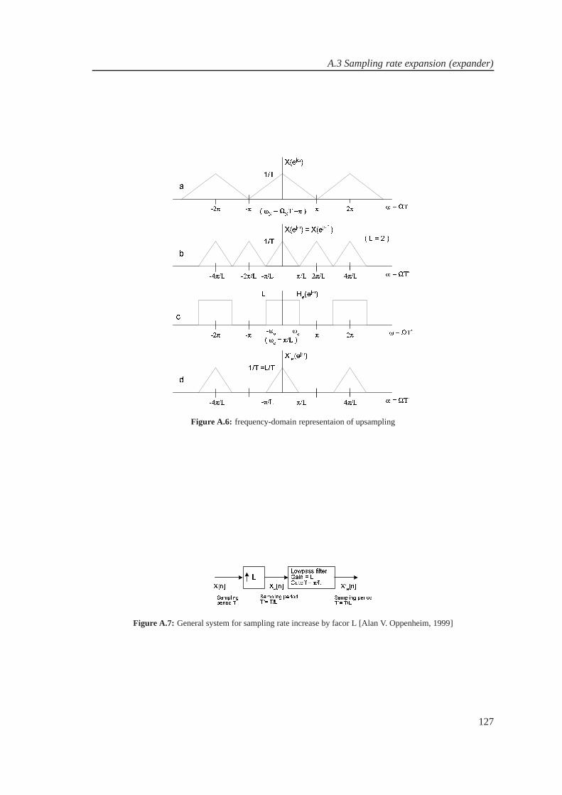
A.3 Sampling rate expansion (expander)
!
"
Figure A.6: frequency-domain representaion of upsampling
# $ %& '( )$ '( )* + , - ./0 1- 2 3 /4 5 6 * + , - . /0 1 - 2 3 /4 56 78 6 9: ; <= > ? @ @ A BCD E FG ? BH I ;J KD< A A I L MN$ & '( ) * + , - ./0 1 - 2 3 /4 56 78 6 9 :Figure A.7: General system for sampling rate increase by facor L [Alan V.Oppenheim, 1999]
127
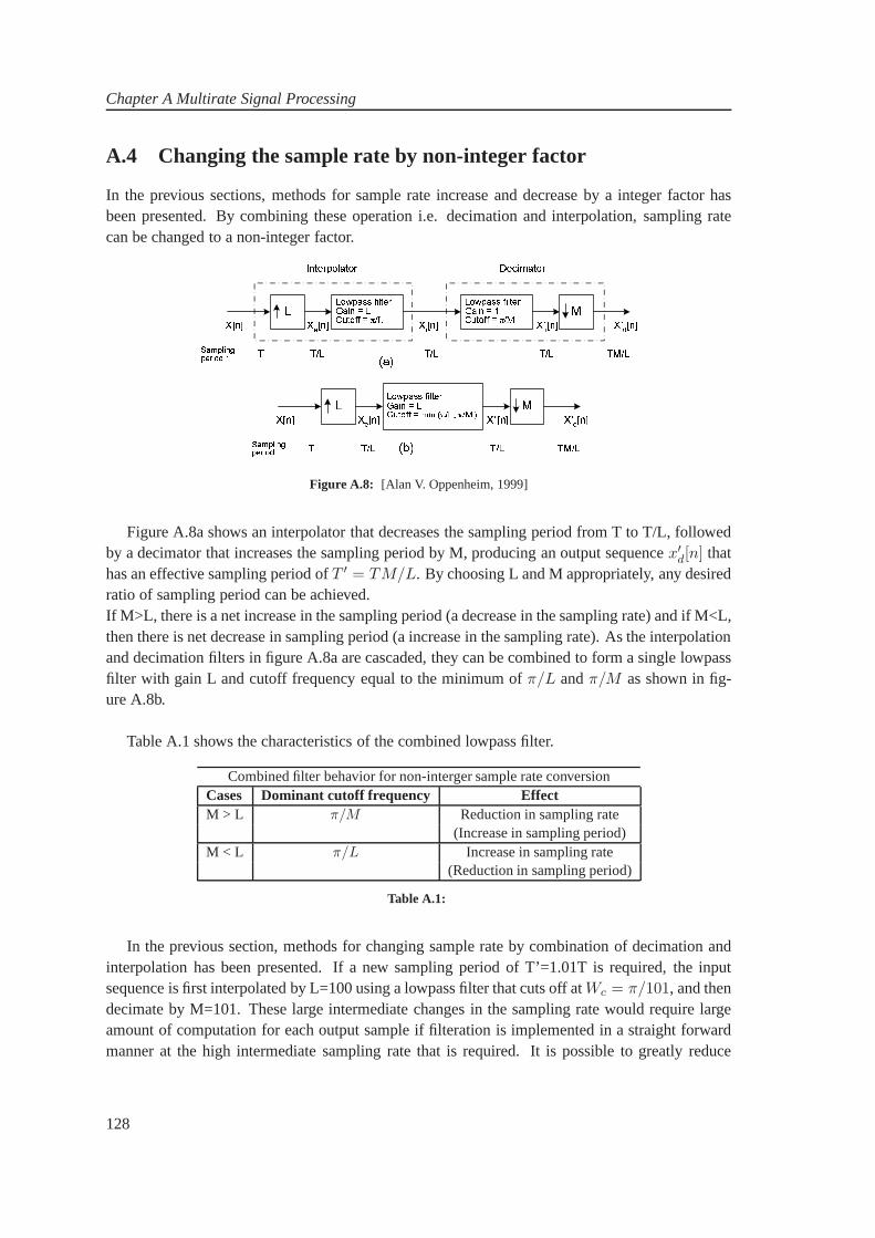
Chapter A Multirate Signal Processing
A.4 Changing the sample rate by non-integer factor
In the previous sections, methods for sample rate increase and decrease by a integer factor hasbeen presented. By combining these operation i.e. decimation and interpolation, sampling ratecan be changed to a non-integer factor. !" # $ % & $ ' () * + !" # $ ,% & $ ' (- . / 0 1 23 4 56 04 2 78 7 9 1 : ;< 6 04 2
* + !" # $ % & $ = >? @' () A ' (- B . 78 7 CD E CF EFigure A.8: [Alan V. Oppenheim, 1999]
Figure A.8a shows an interpolator that decreases the sampling period from T to T/L, followedby a decimator that increases the sampling period by M, producing an output sequencex′
d[n] thathas an effective sampling period ofT ′ = TM/L. By choosing L and M appropriately, any desiredratio of sampling period can be achieved.If M>L, there is a net increase in the sampling period (a decrease in the sampling rate) and if M<L,then there is net decrease in sampling period (a increase in the sampling rate). As the interpolationand decimation filters in figure A.8a are cascaded, they can becombined to form a single lowpassfilter with gain L and cutoff frequency equal to the minimum ofπ/L andπ/M as shown in fig-ure A.8b.
Table A.1 shows the characteristics of the combined lowpassfilter.
Combined filter behavior for non-interger sample rate conversionCases Dominant cutoff frequency EffectM > L π/M Reduction in sampling rate
(Increase in sampling period)M < L π/L Increase in sampling rate
(Reduction in sampling period)
Table A.1:
In the previous section, methods for changing sample rate bycombination of decimation andinterpolation has been presented. If a new sampling period of T’=1.01T is required, the inputsequence is first interpolated by L=100 using a lowpass filterthat cuts off atWc = π/101, and thendecimate by M=101. These large intermediate changes in the sampling rate would require largeamount of computation for each output sample if filteration is implemented in a straight forwardmanner at the high intermediate sampling rate that is required. It is possible to greatly reduce
128

A.5 Polyphase Decomposition
the amount of computation required by taking the advantagesof some basic multirate processingtechniques. These techniques include identities
A.5 Polyphase Decomposition
The polyphase decomposition of a sequence is obtained by representing it as a superposition of Msubsequnces, each consisting of every mth value of successfully delayed version of the sequence.By appling this decomposition to filter impusle respose, efficient implementation structure forlinear filters can be obtained. Conside an impulse responseH[n] that has to be decompose into Msebsequnceshk[n] as follows:
hk[n] =
h[n + k] if n is integer multiple of M0 otherwise
(A.3)
By successfully delaying these subsequences, the originalimpluse responseh[n] can be con-structed; i.e.
h[n] =M−1∑
k=0
hk[n − k] (A.4)
This decomposition can be represented by block diagram as shown in figure A.9. The se-quencesek[n] are
ek[n] = h[nM + k] = hk[nM ] (A.5)
and are reffered as polyphase components of h[n]. Figure A.10 shows a chain of advanceelements at the input and a chain of delay elements at the output and is equivalent to figure A.9.
Figure A.9: Polyphase decomposition of filter h[n] using componentsek[n] [Alan V. Oppenheim, 1999]
Figures A.9 and A.10 are not realization of the filter, but they show the decomposition of filterinto M parallel filters. In frequency or z-domain, the polyphase components are represented as:
H(z) =
M−1∑
k=0
Ek(zM )z−k (A.6)
The equation A.6 expresses the system function H(z) as a sum of delayed polyphase compo-nents filters, as shown in figure A.11.
129

Chapter A Multirate Signal Processing
Figure A.10: Polyphase decomposition of filter h[n] using componentsek[n] with chained de-lays [Alan V. Oppenheim, 1999]
! " # $ % &$ % &$ % &' (
Figure A.11: Realization structure based on polyphase decomposition ofh[n] [Alan V. Oppenheim, 1999]
130
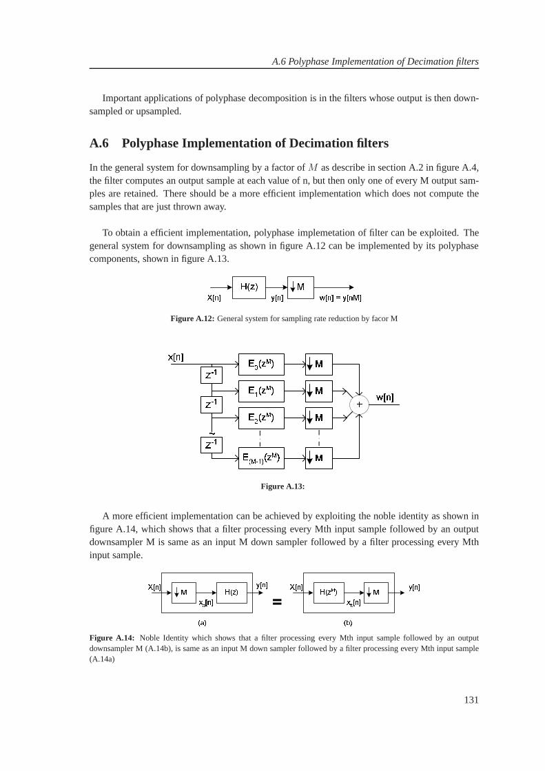
A.6 Polyphase Implementation of Decimation filters
Important applications of polyphase decomposition is in the filters whose output is then down-sampled or upsampled.
A.6 Polyphase Implementation of Decimation filters
In the general system for downsampling by a factor ofM as describe in section A.2 in figure A.4,the filter computes an output sample at each value of n, but then only one of every M output sam-ples are retained. There should be a more efficient implementation which does not compute thesamples that are just thrown away.
To obtain a efficient implementation, polyphase implemetation of filter can be exploited. Thegeneral system for downsampling as shown in figure A.12 can beimplemented by its polyphasecomponents, shown in figure A.13.
Figure A.12: General system for sampling rate reduction by facor M
!!!! "Figure A.13:
A more efficient implementation can be achieved by exploiting the noble identity as shown infigure A.14, which shows that a filter processing every Mth input sample followed by an outputdownsampler M is same as an input M down sampler followed by a filter processing every Mthinput sample. # $ %& '( % & ' ) *+ , - . / % & '# $ % & '( % & ' ) *+ -. 0 % & ' =* 1 - * 2 -Figure A.14: Noble Identity which shows that a filter processing every Mthinput sample followed by an outputdownsampler M (A.14b), is same as an input M down sampler followed by a filter processing every Mth input sample(A.14a)
131
Chapter A Multirate Signal Processing
Applying the nobel identity to decimator structure shown infigure A.13, the resulted efficientstructure is shown in figure A.15. For computational efficiency of the structure shown in fig-ure A.15, consider an input x[n] clocked at a rate of 1 sample per unit time and H(z) an N-pointFIR filter. Straight forward implementation of decimator shown in figure A.12 would require Nmultiplications and (N-1) additions per unit time. In the structure shown in figure A.15, each offilter Ez(k) is of lengthN/M , and their inputs are clocks at the rate of 1 per M units of time. Soeach filter requires1/M(N/M) multiplications per time and(N/M −1)+(M −1) additions perunit time, resulting in significant saving for values of M andN.
Figure A.15:
A.7 Polyphase Implementation of Interpolation filters
An efficient implementation as presented for decimation filters in previous section, can also beachieved for interpolation filters shown in figure. Since only every Lth sample of w[n] is nonzero,the most stsright forward implementation of figure would require applying filter cofficient to se-quence that are known to be zero. So there should be some efficient implementation.
To obtain a efficient implementation, polyphase implemetation of filter can be exploited. Thegeneral system for upsampling as shown in figure can be implemented by its polyphase compo-nents, shown in figure A.13.
Figure A.16: General system for sampling rate increase by factor L
A more efficient implementation can be achieved by exploiting the noble identity for upsam-pling shown in figure , which shows that a filter processing every input sample followed by anoutput upsampler L (A.18b), is same as an input L up sampler followed by a filter processingevery Lth input sample. The resulted rearranged upsampler system is shown in figure A.19.
For computational efficiency of the structure shown in figureA.19, consider an input x[n]clocked at a rate of 1 sample per unit time and H(z) an N-point FIR filter. Straight forward
132
A.7 Polyphase Implementation of Interpolation filters
Figure A.17:
! " # = $ % Figure A.18: Noble Identity for upsamping which shows that a filter processing every input sample followed by anoutput upsampler L (A.18b), is same as an input L up sampler followed by a filter processing every Lth input sample(A.18a).
133

Chapter A Multirate Signal Processing
implementation of upsampler shown in figure A.16 would require NL multiplications and (NL-1) additions per unit time. In the structure shown in figure A.19, each of filterEz(k) requiresL(N/L) multiplications andL(N/L − 1) additions per unit time, plus (L-1) additions to obtainoutputy[n]. It results in a significant saving for values of L and N.
Figure A.19:
Gain in computational efficieny for both the decimation and interpolation results from the re-arranging the operations so that the filtering is done at the low sampling rate.
A.8 Multi-stage filters
Changes in sampling rate can be achieved in single stage using one decimator or interpolator.When large changes in sampling rate is required, it is more efficient to change the rate in twoor more than two stages [Emmanuel C. Ifeachor, 2002]. Most practical multirate systems employthe multistage approach because it allows a gradual change in the sampling rate, leading to asignificant relaxtion in the requirements of anti-aliasingor anti-imaging filter at each stage. Figureshows an I-stage decimator. The overall decimation factor M, is expressed as the product of thesmaller factors:
M = M1 M2 M3 ....... MI = N (A.7)
Each stage is independent as shown in dashed boxes. If M»1 themultistage approach leads tomuch reduced computational and storage requirements, a relaxation in the characteristics of thefilters used in the decimators, and consequently to filters that are less sensitive to finite wordlengtheffects. But these advantages are achieved at the expense ofincreased difficulty in the design andimplemetation of the system [Emmanuel C. Ifeachor, 2002].
The design of a practical multiple stage sample rate converter can be broken down into follow-ing four steps [Emmanuel C. Ifeachor, 2002]:
• Specify the overal anti-aliasing or anti-imaging filters and those for individual stages;
• Determine the optimum number of stages of decimation or interpolation that yield the mostefficient implementation;
134
A.8 Multi-stage filters
• Determine the decimation or interpolation factors for eachstage;
• Design an appropriate filter for each stage.
The performance of multirate system depends critically on the type and quality of the filterused. Either FIR or IIR filters can be used for decimation or interpolation, but the FIR is the morepopular. FIR filters have desirable attributes like linear phase response and low sensitivity to finitewordlength effect, as well as being simple to effect. In particular, the optimal and half-band filtersare widely used [Emmanuel C. Ifeachor, 2002].
135

APPENDIX B
V IRTEX -FPGA
FPGAs are similar to custom designed chips in that they implement specific circuitry for a par-ticular function. The major difference is that a FPGA is configured by a bitstream instead of bybeing hardwired through fabrication at a factory. This means that a FPGA’s internal circuitry maybe altered an unlimited number of times.
FPGAs may be classified as "coarse-grained" or "fine-grained", referring to the number andcomplexity of each basic logic element in the FPGA. Xilinx Virtex series chips are coarse-grained,and have logic units based on look-up tables (LUTs) and registers. The basic Virtex logic elementis a Configurable Logic Block (CLB) slice. Two slices are present in each CLB. Each slice con-tains two 4-input, 1-output LUTs and two registers. The interconnections between these elementsare configured by multiplexers controlled by SRAM cells programmed by a user’s bitstream. TheLUTs allow any function of five inputs, any two functions of four inputs, or some functions of upto nine inputs to be created within a CLB slice. The outputs ofthese functions may be registered,or the registers may be used independently of the LUTs. This structure allows a very powerfulmethod of implementing arbitrary, complex digital logic.
The Xilinx slices also have the ability to implement distributed memory instead of logic. Each4-input LUT in a slice may be used to implement a 16x1 ROM or RAM, or the two LUTs maybe combined together to create a 32x1 ROM or RAM or a 16x1 dual-port RAM. This allows eachslice to trade logic resources for memory in order to maximize the resources available for a partic-ular application.
The CLBs in a Virtex FPGA are connected via programmable interconnect called the generalpurpose routing. This interconnect consists of differing length lines, some connecting adjacentCLBs together, while some span the entire length of the chip and others are designed for high fan-out signals such as clocks. The connections between the interconnect and the CLBS are controlledby switch matrices called general routing matrices (GRMs).The programmable interconnect al-lows mappings that require local communication to be handled efficiently along with requirementsfor arbitrary, longer-distance, routing demands. In addition to the programmable interconnect,there are a few dedicated routing resources. One example is the carry-chains between CLBs that
137

Chapter B Virtex-FPGA
allow high-speed carry propagation through a series of slices, enabling high-speed adders andother arithmetic units to be designed in a chain of CLBs. Connections between the internal rout-ing and the external world are made through Input/Output Blocks, or IOBs, which contain input/output registers and connect directly to a package pin.
The Virtex FPGAs also include Block RAM units on the edges of the FPGA. These resourcesare ideal when large amounts of memory are required that would not use the small, distributedCLB-based memory efficiently. Finally, the Virtex also has advanced clock management resourcesbuilt in, including a delay locked loop (DLL) that reduces clock skew and can divide (by up to 16)or multiply (by 2) external clocks for slower or faster internal clocking.
The highly replicated, register rich architecture of the Virtex makes it suitable for custom com-puting applications. Each slice can perform a two-bit computation or look-up, allowing a systolicstructure of processors to be built out of the regular array of CLBs in a Virtex. There are caseswhen a finer grain structure may be more efficient, as the CLB structure may not be the mostefficient medium for very small systolic-cell based arithmetic.
The VirtexIV-XC4VSX35, has 15,360 CLB slices and 3,456Kb Block RAM. More details canbe seen on Virtex datasheets.
B.1 Computational Unit Implementation
To illustrate the capacity of a slice, two commonly used DSP computational units, an adder anda multiplier, are presented with their area in terms of CLB slices. The Virtex has dedicated fast-carry chain resources built into each CLB. Two adder bits canfit into a single slice so that a b-bitadder consumes b/2 CLB slices. A 16-bit adder would require 8slices. [Xil98a] The Virtex alsohas dedicated multiplication resources so that two multiplication bits can fit into a single slice. Ana-bit by b-bit multiplier requires approximately
b log2b + (b − 1)a2
(B.1)
CLB slices. A 16x16-bit multiplier would require about 152 slices.
138