max77650max77651 ultra-low power pmic with 3-otpt …€¦ · · 2017-07-13configuring a valid...
TRANSCRIPT

General DescriptionThe MAX77650/MAX77651 provide highly-integrated bat-tery charging and power supply solutions for low-power wearable applications where size and efficiency are critical. Both devices feature a SIMO buck-boost regulator that provides three independently programmable power rails from a single inductor to minimize total solution size. A 150mA LDO provides ripple rejection for audio and other noise-sensitive applications. A highly configu-rable linear charger supports a wide range of Li+ battery capacities and includes battery temperature monitoring for additional safety (JEITA).The devices include other features such as current sinks for driving LED indicators and an analog multiplexer that switches several internal voltage and current signals to an external node for monitoring with an external ADC. A bidi-rectional I2C interface allows for configuring and check-ing the status of the devices. An internal on/off controller provides a controlled startup sequence for the regulators and provides supervisory functionality when the devices are on. Numerous factory programmable options allow the device to be tailored for many applications, enabling faster time to market.
Benefits and Features Highly Integrated
• Smart Power Selector™ Li+/Li-Poly Charger• 3 Output, Single-Inductor Multiple-Output (SIMO)
Buck-Boost Regulator• 150mA LDO• 3-Channel Current Sink Driver• Analog MUX Output for Power Monitoring
Low Power• 0.3μA Standby Current• 5.6μA Operating Current (3 SIMO Channels +
LDO) Charger Optimized for Small Battery Size
• Programmable Fast-Charge Current from 7.5mA to 300mA
• Programmable Battery Regulation Voltage from 3.6V to 4.6V
• Programmable Termination Current from 0.375mA to 45mA
• JEITA Battery Temperature Monitors Adjust Charge Current and Battery Regulation Voltage for Safe Charging
Flexible and Configurable• I2C Compatible Interface and GPIO• Factory OTP Options Available
Small Size• 2.75mm x 2.15mm x 0.7mm WLP Package• 30-Bump, 0.4mm-Pitch WLP, 6x5 Array• Small Total Solution Size (19.2mm2)
Applications Bluetooth Headphones/Hearables Fitness, Health, and Activity Monitors Portable Devices Internet of Things (IoT)
Ordering Information appears at end of data sheet.
19-8550; Rev 4; 7/17
Smart Power Selector is a trademark of Maxim Integrated Products, Inc.
Simplified System Diagram
PWR_HLD
GPIO
VBUSCHGIN VSYSSYS
GND
PGND
2.05VSBB0
1.2VSBB1
1.5µHLXALXB
VIO
SDASCL
nIRQ
IN_LDO
1.85VLDO
nENnRST
3.3VSBB2
LED0
LED1
LED2PROCESSOR
VIO/POWER
SYS
ADC INPUT
MAX77650
PWR_HLD
nRST
SDASCL
nIRQ
SYSTEM RESOURCES
IN_SBB
GPIO
**
AMUX AMUX
BATT+
THMTBIAS
**
*THIS DRAWING ASSUMES THAT THE PROCESSOR HAS INTERNAL PULLUPRESISTORS FOR THIS NODE.
MAX77650/MAX77651 Ultra-Low Power PMIC with 3-Output SIMO and Charger Optimized for Small Li+
EVALUATION KIT AVAILABLE
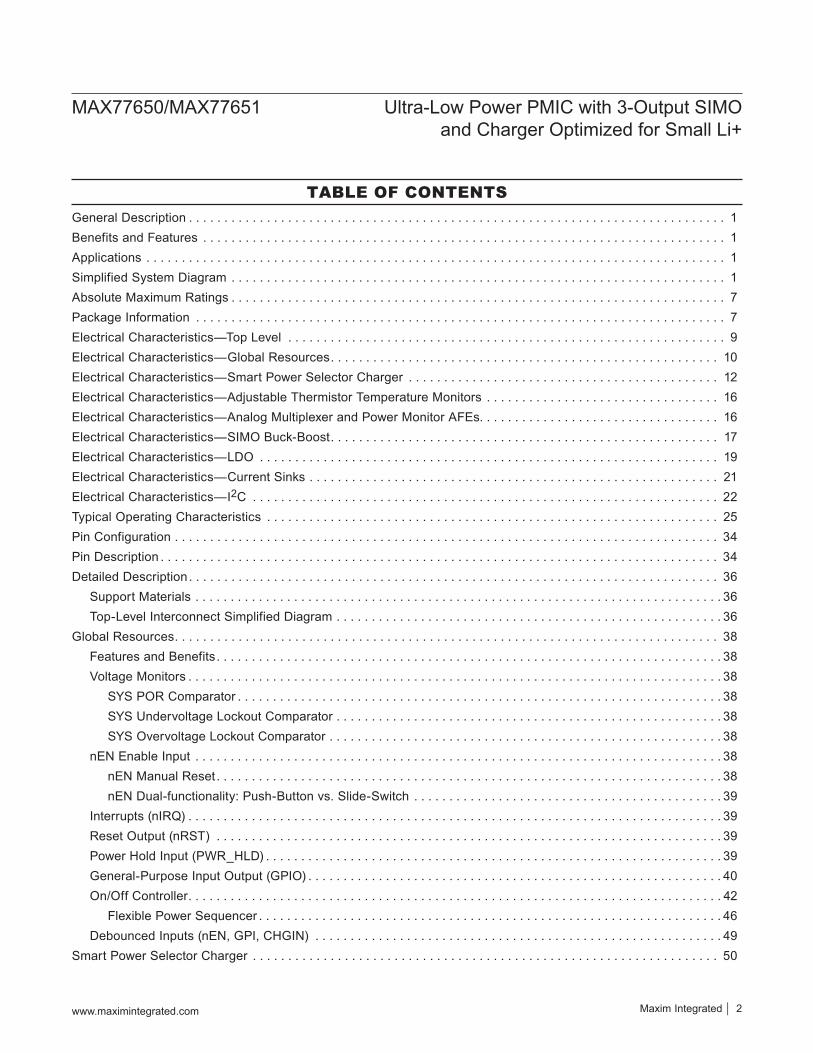
General Description . . . . . . . . . . . . . . . . . . . . . . . . . . . . . . . . . . . . . . . . . . . . . . . . . . . . . . . . . . . . . . . . . . . . . . . . . . . . 1Benefits and Features . . . . . . . . . . . . . . . . . . . . . . . . . . . . . . . . . . . . . . . . . . . . . . . . . . . . . . . . . . . . . . . . . . . . . . . . . . 1Applications . . . . . . . . . . . . . . . . . . . . . . . . . . . . . . . . . . . . . . . . . . . . . . . . . . . . . . . . . . . . . . . . . . . . . . . . . . . . . . . . . . 1Simplified System Diagram . . . . . . . . . . . . . . . . . . . . . . . . . . . . . . . . . . . . . . . . . . . . . . . . . . . . . . . . . . . . . . . . . . . . . . 1Absolute Maximum Ratings . . . . . . . . . . . . . . . . . . . . . . . . . . . . . . . . . . . . . . . . . . . . . . . . . . . . . . . . . . . . . . . . . . . . . . 7Package Information . . . . . . . . . . . . . . . . . . . . . . . . . . . . . . . . . . . . . . . . . . . . . . . . . . . . . . . . . . . . . . . . . . . . . . . . . . . 7Electrical Characteristics—Top Level . . . . . . . . . . . . . . . . . . . . . . . . . . . . . . . . . . . . . . . . . . . . . . . . . . . . . . . . . . . . . . 9Electrical Characteristics—Global Resources. . . . . . . . . . . . . . . . . . . . . . . . . . . . . . . . . . . . . . . . . . . . . . . . . . . . . . . 10Electrical Characteristics—Smart Power Selector Charger . . . . . . . . . . . . . . . . . . . . . . . . . . . . . . . . . . . . . . . . . . . . 12Electrical Characteristics—Adjustable Thermistor Temperature Monitors . . . . . . . . . . . . . . . . . . . . . . . . . . . . . . . . . 16Electrical Characteristics—Analog Multiplexer and Power Monitor AFEs. . . . . . . . . . . . . . . . . . . . . . . . . . . . . . . . . . 16Electrical Characteristics—SIMO Buck-Boost. . . . . . . . . . . . . . . . . . . . . . . . . . . . . . . . . . . . . . . . . . . . . . . . . . . . . . . 17Electrical Characteristics—LDO . . . . . . . . . . . . . . . . . . . . . . . . . . . . . . . . . . . . . . . . . . . . . . . . . . . . . . . . . . . . . . . . . 19Electrical Characteristics—Current Sinks . . . . . . . . . . . . . . . . . . . . . . . . . . . . . . . . . . . . . . . . . . . . . . . . . . . . . . . . . . 21Electrical Characteristics—I2C . . . . . . . . . . . . . . . . . . . . . . . . . . . . . . . . . . . . . . . . . . . . . . . . . . . . . . . . . . . . . . . . . . 22Typical Operating Characteristics . . . . . . . . . . . . . . . . . . . . . . . . . . . . . . . . . . . . . . . . . . . . . . . . . . . . . . . . . . . . . . . . 25Pin Configuration . . . . . . . . . . . . . . . . . . . . . . . . . . . . . . . . . . . . . . . . . . . . . . . . . . . . . . . . . . . . . . . . . . . . . . . . . . . . . 34Pin Description . . . . . . . . . . . . . . . . . . . . . . . . . . . . . . . . . . . . . . . . . . . . . . . . . . . . . . . . . . . . . . . . . . . . . . . . . . . . . . . 34Detailed Description. . . . . . . . . . . . . . . . . . . . . . . . . . . . . . . . . . . . . . . . . . . . . . . . . . . . . . . . . . . . . . . . . . . . . . . . . . . 36
Support Materials . . . . . . . . . . . . . . . . . . . . . . . . . . . . . . . . . . . . . . . . . . . . . . . . . . . . . . . . . . . . . . . . . . . . . . . . . . . 36Top-Level Interconnect Simplified Diagram . . . . . . . . . . . . . . . . . . . . . . . . . . . . . . . . . . . . . . . . . . . . . . . . . . . . . . . 36
Global Resources. . . . . . . . . . . . . . . . . . . . . . . . . . . . . . . . . . . . . . . . . . . . . . . . . . . . . . . . . . . . . . . . . . . . . . . . . . . . . 38Features and Benefits. . . . . . . . . . . . . . . . . . . . . . . . . . . . . . . . . . . . . . . . . . . . . . . . . . . . . . . . . . . . . . . . . . . . . . . . 38Voltage Monitors . . . . . . . . . . . . . . . . . . . . . . . . . . . . . . . . . . . . . . . . . . . . . . . . . . . . . . . . . . . . . . . . . . . . . . . . . . . . 38
SYS POR Comparator . . . . . . . . . . . . . . . . . . . . . . . . . . . . . . . . . . . . . . . . . . . . . . . . . . . . . . . . . . . . . . . . . . . . . 38SYS Undervoltage Lockout Comparator . . . . . . . . . . . . . . . . . . . . . . . . . . . . . . . . . . . . . . . . . . . . . . . . . . . . . . . 38SYS Overvoltage Lockout Comparator . . . . . . . . . . . . . . . . . . . . . . . . . . . . . . . . . . . . . . . . . . . . . . . . . . . . . . . . 38
nEN Enable Input . . . . . . . . . . . . . . . . . . . . . . . . . . . . . . . . . . . . . . . . . . . . . . . . . . . . . . . . . . . . . . . . . . . . . . . . . . . 38nEN Manual Reset . . . . . . . . . . . . . . . . . . . . . . . . . . . . . . . . . . . . . . . . . . . . . . . . . . . . . . . . . . . . . . . . . . . . . . . . 38nEN Dual-functionality: Push-Button vs. Slide-Switch . . . . . . . . . . . . . . . . . . . . . . . . . . . . . . . . . . . . . . . . . . . . 39
Interrupts (nIRQ) . . . . . . . . . . . . . . . . . . . . . . . . . . . . . . . . . . . . . . . . . . . . . . . . . . . . . . . . . . . . . . . . . . . . . . . . . . . . 39Reset Output (nRST) . . . . . . . . . . . . . . . . . . . . . . . . . . . . . . . . . . . . . . . . . . . . . . . . . . . . . . . . . . . . . . . . . . . . . . . . 39Power Hold Input (PWR_HLD) . . . . . . . . . . . . . . . . . . . . . . . . . . . . . . . . . . . . . . . . . . . . . . . . . . . . . . . . . . . . . . . . . 39General-Purpose Input Output (GPIO) . . . . . . . . . . . . . . . . . . . . . . . . . . . . . . . . . . . . . . . . . . . . . . . . . . . . . . . . . . . 40On/Off Controller. . . . . . . . . . . . . . . . . . . . . . . . . . . . . . . . . . . . . . . . . . . . . . . . . . . . . . . . . . . . . . . . . . . . . . . . . . . . 42
Flexible Power Sequencer . . . . . . . . . . . . . . . . . . . . . . . . . . . . . . . . . . . . . . . . . . . . . . . . . . . . . . . . . . . . . . . . . . 46Debounced Inputs (nEN, GPI, CHGIN) . . . . . . . . . . . . . . . . . . . . . . . . . . . . . . . . . . . . . . . . . . . . . . . . . . . . . . . . . . 49
Smart Power Selector Charger . . . . . . . . . . . . . . . . . . . . . . . . . . . . . . . . . . . . . . . . . . . . . . . . . . . . . . . . . . . . . . . . . . 50
TABLE OF CONTENTS
www.maximintegrated.com Maxim Integrated 2
MAX77650/MAX77651 Ultra-Low Power PMIC with 3-Output SIMO and Charger Optimized for Small Li+

Features . . . . . . . . . . . . . . . . . . . . . . . . . . . . . . . . . . . . . . . . . . . . . . . . . . . . . . . . . . . . . . . . . . . . . . . . . . . . . . . . . . 50Charger Symbol Reference Guide . . . . . . . . . . . . . . . . . . . . . . . . . . . . . . . . . . . . . . . . . . . . . . . . . . . . . . . . . . . . . . 51Smart Power Selector . . . . . . . . . . . . . . . . . . . . . . . . . . . . . . . . . . . . . . . . . . . . . . . . . . . . . . . . . . . . . . . . . . . . . . . . 52Input Current Limiter . . . . . . . . . . . . . . . . . . . . . . . . . . . . . . . . . . . . . . . . . . . . . . . . . . . . . . . . . . . . . . . . . . . . . . . . . 52Minimum Input Voltage Regulation . . . . . . . . . . . . . . . . . . . . . . . . . . . . . . . . . . . . . . . . . . . . . . . . . . . . . . . . . . . . . . 52Minimum System Voltage Regulation . . . . . . . . . . . . . . . . . . . . . . . . . . . . . . . . . . . . . . . . . . . . . . . . . . . . . . . . . . . . 52Die Temperature Regulation . . . . . . . . . . . . . . . . . . . . . . . . . . . . . . . . . . . . . . . . . . . . . . . . . . . . . . . . . . . . . . . . . . . 52Charger State Machine . . . . . . . . . . . . . . . . . . . . . . . . . . . . . . . . . . . . . . . . . . . . . . . . . . . . . . . . . . . . . . . . . . . . . . . 53
Charger Off State. . . . . . . . . . . . . . . . . . . . . . . . . . . . . . . . . . . . . . . . . . . . . . . . . . . . . . . . . . . . . . . . . . . . . . . . . 54Prequalification State. . . . . . . . . . . . . . . . . . . . . . . . . . . . . . . . . . . . . . . . . . . . . . . . . . . . . . . . . . . . . . . . . . . . . . 54Fast-Charge States . . . . . . . . . . . . . . . . . . . . . . . . . . . . . . . . . . . . . . . . . . . . . . . . . . . . . . . . . . . . . . . . . . . . . . . 54Top-Off State . . . . . . . . . . . . . . . . . . . . . . . . . . . . . . . . . . . . . . . . . . . . . . . . . . . . . . . . . . . . . . . . . . . . . . . . . . . . 54Done State . . . . . . . . . . . . . . . . . . . . . . . . . . . . . . . . . . . . . . . . . . . . . . . . . . . . . . . . . . . . . . . . . . . . . . . . . . . . . . 54Prequalification Timer Fault State . . . . . . . . . . . . . . . . . . . . . . . . . . . . . . . . . . . . . . . . . . . . . . . . . . . . . . . . . . . . 54Fast-Charge Timer Fault State . . . . . . . . . . . . . . . . . . . . . . . . . . . . . . . . . . . . . . . . . . . . . . . . . . . . . . . . . . . . . . 55Battery Temperature Fault State . . . . . . . . . . . . . . . . . . . . . . . . . . . . . . . . . . . . . . . . . . . . . . . . . . . . . . . . . . . . . 55JEITA-Modified States . . . . . . . . . . . . . . . . . . . . . . . . . . . . . . . . . . . . . . . . . . . . . . . . . . . . . . . . . . . . . . . . . . . . . 55Typical Charge Profile . . . . . . . . . . . . . . . . . . . . . . . . . . . . . . . . . . . . . . . . . . . . . . . . . . . . . . . . . . . . . . . . . . . . . 55
Charger Applications Information . . . . . . . . . . . . . . . . . . . . . . . . . . . . . . . . . . . . . . . . . . . . . . . . . . . . . . . . . . . . . . . 56Configuring a Valid System Voltage . . . . . . . . . . . . . . . . . . . . . . . . . . . . . . . . . . . . . . . . . . . . . . . . . . . . . . . . . . 56CHGIN/SYS/BATT Capacitor Selection. . . . . . . . . . . . . . . . . . . . . . . . . . . . . . . . . . . . . . . . . . . . . . . . . . . . . . . . 56
Adjustable Thermistor Temperature Monitors . . . . . . . . . . . . . . . . . . . . . . . . . . . . . . . . . . . . . . . . . . . . . . . . . . . . . . . 57Thermistor Bias . . . . . . . . . . . . . . . . . . . . . . . . . . . . . . . . . . . . . . . . . . . . . . . . . . . . . . . . . . . . . . . . . . . . . . . . . . . . . 59Configurable Temperature Thresholds . . . . . . . . . . . . . . . . . . . . . . . . . . . . . . . . . . . . . . . . . . . . . . . . . . . . . . . . . . . 59Thermistor Applications Information . . . . . . . . . . . . . . . . . . . . . . . . . . . . . . . . . . . . . . . . . . . . . . . . . . . . . . . . . . . . . 60
Using Different Thermistor β . . . . . . . . . . . . . . . . . . . . . . . . . . . . . . . . . . . . . . . . . . . . . . . . . . . . . . . . . . . . . . . . 60NTC Thermistor Selection . . . . . . . . . . . . . . . . . . . . . . . . . . . . . . . . . . . . . . . . . . . . . . . . . . . . . . . . . . . . . . . . . . 60
Analog Multiplexer & Power Monitor AFEs . . . . . . . . . . . . . . . . . . . . . . . . . . . . . . . . . . . . . . . . . . . . . . . . . . . . . . . . . 61Measuring Battery Current . . . . . . . . . . . . . . . . . . . . . . . . . . . . . . . . . . . . . . . . . . . . . . . . . . . . . . . . . . . . . . . . . . . . 62
Method for Measuring Discharging Current . . . . . . . . . . . . . . . . . . . . . . . . . . . . . . . . . . . . . . . . . . . . . . . . . . . . 62Method for Measuring Charging Current . . . . . . . . . . . . . . . . . . . . . . . . . . . . . . . . . . . . . . . . . . . . . . . . . . . . . . . 62
SIMO Buck-Boost. . . . . . . . . . . . . . . . . . . . . . . . . . . . . . . . . . . . . . . . . . . . . . . . . . . . . . . . . . . . . . . . . . . . . . . . . . . . . 63SIMO Benefits and Features . . . . . . . . . . . . . . . . . . . . . . . . . . . . . . . . . . . . . . . . . . . . . . . . . . . . . . . . . . . . . . . . . . 63SIMO Control Scheme . . . . . . . . . . . . . . . . . . . . . . . . . . . . . . . . . . . . . . . . . . . . . . . . . . . . . . . . . . . . . . . . . . . . . . . 64SIMO Soft-Start . . . . . . . . . . . . . . . . . . . . . . . . . . . . . . . . . . . . . . . . . . . . . . . . . . . . . . . . . . . . . . . . . . . . . . . . . . . . 64SIMO Registers. . . . . . . . . . . . . . . . . . . . . . . . . . . . . . . . . . . . . . . . . . . . . . . . . . . . . . . . . . . . . . . . . . . . . . . . . . . . . 64SIMO Active Discharge Resistance . . . . . . . . . . . . . . . . . . . . . . . . . . . . . . . . . . . . . . . . . . . . . . . . . . . . . . . . . . . . . 64SIMO Applications Information . . . . . . . . . . . . . . . . . . . . . . . . . . . . . . . . . . . . . . . . . . . . . . . . . . . . . . . . . . . . . . . . . 65
SIMO Available Output Current . . . . . . . . . . . . . . . . . . . . . . . . . . . . . . . . . . . . . . . . . . . . . . . . . . . . . . . . . . . . . . 65
TABLE OF CONTENTS (CONTINUED)
www.maximintegrated.com Maxim Integrated 3
MAX77650/MAX77651 Ultra-Low Power PMIC with 3-Output SIMO and Charger Optimized for Small Li+

TABLE OF CONTENTS (CONTINUED)Inductor Selection . . . . . . . . . . . . . . . . . . . . . . . . . . . . . . . . . . . . . . . . . . . . . . . . . . . . . . . . . . . . . . . . . . . . . . . . 65Input Capacitor Selection. . . . . . . . . . . . . . . . . . . . . . . . . . . . . . . . . . . . . . . . . . . . . . . . . . . . . . . . . . . . . . . . . . . 66Boost Capacitor Selection . . . . . . . . . . . . . . . . . . . . . . . . . . . . . . . . . . . . . . . . . . . . . . . . . . . . . . . . . . . . . . . . . . 66Output Capacitor Selection . . . . . . . . . . . . . . . . . . . . . . . . . . . . . . . . . . . . . . . . . . . . . . . . . . . . . . . . . . . . . . . . . 66SIMO Switching Frequency . . . . . . . . . . . . . . . . . . . . . . . . . . . . . . . . . . . . . . . . . . . . . . . . . . . . . . . . . . . . . . . . . 66Unused Outputs . . . . . . . . . . . . . . . . . . . . . . . . . . . . . . . . . . . . . . . . . . . . . . . . . . . . . . . . . . . . . . . . . . . . . . . . . . 67
LDO . . . . . . . . . . . . . . . . . . . . . . . . . . . . . . . . . . . . . . . . . . . . . . . . . . . . . . . . . . . . . . . . . . . . . . . . . . . . . . . . . . . . . . . 67Features . . . . . . . . . . . . . . . . . . . . . . . . . . . . . . . . . . . . . . . . . . . . . . . . . . . . . . . . . . . . . . . . . . . . . . . . . . . . . . . . . . 67LDO Simplified Block Diagram . . . . . . . . . . . . . . . . . . . . . . . . . . . . . . . . . . . . . . . . . . . . . . . . . . . . . . . . . . . . . . . . . 67LDO Active Discharge Resistor . . . . . . . . . . . . . . . . . . . . . . . . . . . . . . . . . . . . . . . . . . . . . . . . . . . . . . . . . . . . . . . . 67LDO Soft-Start . . . . . . . . . . . . . . . . . . . . . . . . . . . . . . . . . . . . . . . . . . . . . . . . . . . . . . . . . . . . . . . . . . . . . . . . . . . . . 68LDO Applications Information . . . . . . . . . . . . . . . . . . . . . . . . . . . . . . . . . . . . . . . . . . . . . . . . . . . . . . . . . . . . . . . . . . 68
Input and Output Capacitor Selection . . . . . . . . . . . . . . . . . . . . . . . . . . . . . . . . . . . . . . . . . . . . . . . . . . . . . . . . . 68Current Sink Applications Information . . . . . . . . . . . . . . . . . . . . . . . . . . . . . . . . . . . . . . . . . . . . . . . . . . . . . . . . . . . 70
LED Assignment . . . . . . . . . . . . . . . . . . . . . . . . . . . . . . . . . . . . . . . . . . . . . . . . . . . . . . . . . . . . . . . . . . . . . . . . . 70Unused Current Sink Ports . . . . . . . . . . . . . . . . . . . . . . . . . . . . . . . . . . . . . . . . . . . . . . . . . . . . . . . . . . . . . . . . . 70
I2C . . . . . . . . . . . . . . . . . . . . . . . . . . . . . . . . . . . . . . . . . . . . . . . . . . . . . . . . . . . . . . . . . . . . . . . . . . . . . . . . . . . . . . . . 71I2C System Configuration . . . . . . . . . . . . . . . . . . . . . . . . . . . . . . . . . . . . . . . . . . . . . . . . . . . . . . . . . . . . . . . . . . . . . 72I2C Interface Power. . . . . . . . . . . . . . . . . . . . . . . . . . . . . . . . . . . . . . . . . . . . . . . . . . . . . . . . . . . . . . . . . . . . . . . . . . 72I2C Data Transfer . . . . . . . . . . . . . . . . . . . . . . . . . . . . . . . . . . . . . . . . . . . . . . . . . . . . . . . . . . . . . . . . . . . . . . . . . . . 72I2C Start and Stop Conditions . . . . . . . . . . . . . . . . . . . . . . . . . . . . . . . . . . . . . . . . . . . . . . . . . . . . . . . . . . . . . . . . . 72I2C Acknowledge Bit . . . . . . . . . . . . . . . . . . . . . . . . . . . . . . . . . . . . . . . . . . . . . . . . . . . . . . . . . . . . . . . . . . . . . . . . . 73I2C Slave Address. . . . . . . . . . . . . . . . . . . . . . . . . . . . . . . . . . . . . . . . . . . . . . . . . . . . . . . . . . . . . . . . . . . . . . . . . . . 73I2C Clock Stretching . . . . . . . . . . . . . . . . . . . . . . . . . . . . . . . . . . . . . . . . . . . . . . . . . . . . . . . . . . . . . . . . . . . . . . . . . 74I2C General Call Address . . . . . . . . . . . . . . . . . . . . . . . . . . . . . . . . . . . . . . . . . . . . . . . . . . . . . . . . . . . . . . . . . . . . . 74I2C Device ID . . . . . . . . . . . . . . . . . . . . . . . . . . . . . . . . . . . . . . . . . . . . . . . . . . . . . . . . . . . . . . . . . . . . . . . . . . . . . . 74I2C Communication Speed . . . . . . . . . . . . . . . . . . . . . . . . . . . . . . . . . . . . . . . . . . . . . . . . . . . . . . . . . . . . . . . . . . . . 74I2C Communication Protocols. . . . . . . . . . . . . . . . . . . . . . . . . . . . . . . . . . . . . . . . . . . . . . . . . . . . . . . . . . . . . . . . . . 75
Writing to a Single Register . . . . . . . . . . . . . . . . . . . . . . . . . . . . . . . . . . . . . . . . . . . . . . . . . . . . . . . . . . . . . . . . . 75Writing Multiple Bytes to Sequential Registers . . . . . . . . . . . . . . . . . . . . . . . . . . . . . . . . . . . . . . . . . . . . . . . . . . 76Reading from a Single Register. . . . . . . . . . . . . . . . . . . . . . . . . . . . . . . . . . . . . . . . . . . . . . . . . . . . . . . . . . . . . . 77Reading from Sequential Registers . . . . . . . . . . . . . . . . . . . . . . . . . . . . . . . . . . . . . . . . . . . . . . . . . . . . . . . . . . . 77Engaging HS-mode for operation up to 3.4MHz . . . . . . . . . . . . . . . . . . . . . . . . . . . . . . . . . . . . . . . . . . . . . . . . . 78
Typical Application Circuit . . . . . . . . . . . . . . . . . . . . . . . . . . . . . . . . . . . . . . . . . . . . . . . . . . . . . . . . . . . . . . . . . . . . . . 79Ordering Information . . . . . . . . . . . . . . . . . . . . . . . . . . . . . . . . . . . . . . . . . . . . . . . . . . . . . . . . . . . . . . . . . . . . . . . . . . 80Revision History . . . . . . . . . . . . . . . . . . . . . . . . . . . . . . . . . . . . . . . . . . . . . . . . . . . . . . . . . . . . . . . . . . . . . . . . . . . . . . 81
www.maximintegrated.com Maxim Integrated 4
MAX77650/MAX77651 Ultra-Low Power PMIC with 3-Output SIMO and Charger Optimized for Small Li+

LIST OF FIGURESFigure 1. Top-Level Interconnect Simplified Diagram . . . . . . . . . . . . . . . . . . . . . . . . . . . . . . . . . . . . . . . . . . . . . . . . . 37Figure 2. nEN Usage Timing Diagram. . . . . . . . . . . . . . . . . . . . . . . . . . . . . . . . . . . . . . . . . . . . . . . . . . . . . . . . . . . . . 39Figure 3. GPIO Block Diagram . . . . . . . . . . . . . . . . . . . . . . . . . . . . . . . . . . . . . . . . . . . . . . . . . . . . . . . . . . . . . . . . . . .41Figure 4. Top-Level On/Off Controller . . . . . . . . . . . . . . . . . . . . . . . . . . . . . . . . . . . . . . . . . . . . . . . . . . . . . . . . . . . . . 43Figure 5. Power-Up/Power-Down Sequence . . . . . . . . . . . . . . . . . . . . . . . . . . . . . . . . . . . . . . . . . . . . . . . . . . . . . . . . 45Figure 6. Flexible Power Sequencer Basic Timing Diagram . . . . . . . . . . . . . . . . . . . . . . . . . . . . . . . . . . . . . . . . . . . . 46Figure 7. Startup Timing Diagram Due to nEN . . . . . . . . . . . . . . . . . . . . . . . . . . . . . . . . . . . . . . . . . . . . . . . . . . . . . . 47Figure 8. Startup Timing Diagram Due to Charge Source Insertion . . . . . . . . . . . . . . . . . . . . . . . . . . . . . . . . . . . . . . 48Figure 9. Debounced Inputs. . . . . . . . . . . . . . . . . . . . . . . . . . . . . . . . . . . . . . . . . . . . . . . . . . . . . . . . . . . . . . . . . . . . . 49Figure 10. Linear Charger Simplified Block Diagram . . . . . . . . . . . . . . . . . . . . . . . . . . . . . . . . . . . . . . . . . . . . . . . . . 50Figure 11. Charger Simplified Control Loops. . . . . . . . . . . . . . . . . . . . . . . . . . . . . . . . . . . . . . . . . . . . . . . . . . . . . . . . 51Figure 12. Charger State Diagram. . . . . . . . . . . . . . . . . . . . . . . . . . . . . . . . . . . . . . . . . . . . . . . . . . . . . . . . . . . . . . . . 53Figure 13. Example Battery Charge Profile . . . . . . . . . . . . . . . . . . . . . . . . . . . . . . . . . . . . . . . . . . . . . . . . . . . . . . . . . 55Figure 14. Thermistor Logic Functional Diagram. . . . . . . . . . . . . . . . . . . . . . . . . . . . . . . . . . . . . . . . . . . . . . . . . . . . . 57Figure 15. Safe-Charging Profile Example . . . . . . . . . . . . . . . . . . . . . . . . . . . . . . . . . . . . . . . . . . . . . . . . . . . . . . . . . 58Figure 16. Thermistor Bias State Diagram. . . . . . . . . . . . . . . . . . . . . . . . . . . . . . . . . . . . . . . . . . . . . . . . . . . . . . . . . . 59Figure 17. Thermistor Circuit with Adjusting Series and Parallel Resistors. . . . . . . . . . . . . . . . . . . . . . . . . . . . . . . . . 60Figure 18. SIMO Detailed Block Diagram . . . . . . . . . . . . . . . . . . . . . . . . . . . . . . . . . . . . . . . . . . . . . . . . . . . . . . . . . . 63Figure 19. LDO Capacitance for Stability . . . . . . . . . . . . . . . . . . . . . . . . . . . . . . . . . . . . . . . . . . . . . . . . . . . . . . . . . . 69Figure 20. LDO Simplified Block Diagram . . . . . . . . . . . . . . . . . . . . . . . . . . . . . . . . . . . . . . . . . . . . . . . . . . . . . . . . . . 69Figure 21. Current Sink Block Diagram . . . . . . . . . . . . . . . . . . . . . . . . . . . . . . . . . . . . . . . . . . . . . . . . . . . . . . . . . . . . 70Figure 22. I2C Simplified Block Diagram . . . . . . . . . . . . . . . . . . . . . . . . . . . . . . . . . . . . . . . . . . . . . . . . . . . . . . . . . . . 71Figure 23. I2C System Configuration . . . . . . . . . . . . . . . . . . . . . . . . . . . . . . . . . . . . . . . . . . . . . . . . . . . . . . . . . . . . . . 72Figure 24. I2 C Start and Stop Conditions . . . . . . . . . . . . . . . . . . . . . . . . . . . . . . . . . . . . . . . . . . . . . . . . . . . . . . . . . . 72Figure 25. Acknowledge Bit . . . . . . . . . . . . . . . . . . . . . . . . . . . . . . . . . . . . . . . . . . . . . . . . . . . . . . . . . . . . . . . . . . . . . 73Figure 26. Slave Address Example . . . . . . . . . . . . . . . . . . . . . . . . . . . . . . . . . . . . . . . . . . . . . . . . . . . . . . . . . . . . . . . 73Figure 27. Writing to a Single Register with the Write Byte Protocol. . . . . . . . . . . . . . . . . . . . . . . . . . . . . . . . . . . . . . 75Figure 28. Writing to Sequential registers X to N . . . . . . . . . . . . . . . . . . . . . . . . . . . . . . . . . . . . . . . . . . . . . . . . . . . . 76Figure 29. Reading from a Single Register with the Read Byte Protocol . . . . . . . . . . . . . . . . . . . . . . . . . . . . . . . . . . 77Figure 30. Reading Continuously from Sequential Registers X to N. . . . . . . . . . . . . . . . . . . . . . . . . . . . . . . . . . . . . . 77Figure 31. Engaging HS Mode. . . . . . . . . . . . . . . . . . . . . . . . . . . . . . . . . . . . . . . . . . . . . . . . . . . . . . . . . . . . . . . . . . . 78
www.maximintegrated.com Maxim Integrated 5
MAX77650/MAX77651 Ultra-Low Power PMIC with 3-Output SIMO and Charger Optimized for Small Li+

LIST OF TABLESTable 1. Regulator Summary . . . . . . . . . . . . . . . . . . . . . . . . . . . . . . . . . . . . . . . . . . . . . . . . . . . . . . . . . . . . . . . . . . . . 36Table 2. On/Off Controller Transition/State . . . . . . . . . . . . . . . . . . . . . . . . . . . . . . . . . . . . . . . . . . . . . . . . . . . . . . . . . 44Table 3. Charger Quick Symbol Reference Guide. . . . . . . . . . . . . . . . . . . . . . . . . . . . . . . . . . . . . . . . . . . . . . . . . . . . 51Table 4. Trip Temperatures vs. Trip Voltages for Different NTC β. . . . . . . . . . . . . . . . . . . . . . . . . . . . . . . . . . . . . . . . 59Table 5. Example RS and RP Correcting Values for NTC β Above 3380K . . . . . . . . . . . . . . . . . . . . . . . . . . . . . . . . 60Table 6. NTC Thermistors . . . . . . . . . . . . . . . . . . . . . . . . . . . . . . . . . . . . . . . . . . . . . . . . . . . . . . . . . . . . . . . . . . . . . . 60Table 7. AMUX Signal Transfer Functions . . . . . . . . . . . . . . . . . . . . . . . . . . . . . . . . . . . . . . . . . . . . . . . . . . . . . . . . . . 61Table 8. Battery Current Direction Decode . . . . . . . . . . . . . . . . . . . . . . . . . . . . . . . . . . . . . . . . . . . . . . . . . . . . . . . . . 62Table 9. SIMO Available Output Current for Common Applications . . . . . . . . . . . . . . . . . . . . . . . . . . . . . . . . . . . . . . 65Table 10. Example Inductors . . . . . . . . . . . . . . . . . . . . . . . . . . . . . . . . . . . . . . . . . . . . . . . . . . . . . . . . . . . . . . . . . . . . 65Table 11. I2C Slave Address Options. . . . . . . . . . . . . . . . . . . . . . . . . . . . . . . . . . . . . . . . . . . . . . . . . . . . . . . . . . . . . . .74
www.maximintegrated.com Maxim Integrated 6
MAX77650/MAX77651 Ultra-Low Power PMIC with 3-Output SIMO and Charger Optimized for Small Li+
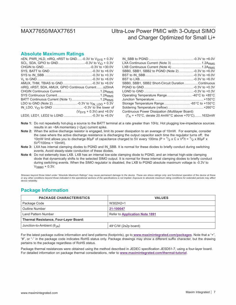
nEN, PWR_HLD, nIRQ, nRST to GND .....-0.3V to VSYS + 0.3VSCL, SDA, GPIO to GND .............................-0.3V to VIO + 0.3VCHGIN to GND ...................................................-0.3V to +30.0VSYS, BATT to GND ..............................................-0.3V to +6.0VSYS to IN_SBB ....................................................-0.3V to +0.3VVL to GND ............................................................-0.3V to +6.0VAMUX, THM, TBIAS to GND ................................-0.3V to +6.0VnIRQ, nRST, SDA, AMUX, GPIO Continous Current .......±20mACHGIN Continuous Current...........................................1.2ARMSSYS Continuous Current ...............................................1.2ARMSBATT Continuous Current (Note 1) ...............................1.2ARMSLDO to GND (Note 2) ...........................-0.3V to VIN_LDO + 0.3VIN_LDO, VIO to GND ................................. -0.3V to the lower of
(VSYS + 0.3V) and +6.0VLED0, LED1, LED2 to LGND ...............................-0.3V to +6.0V
IN_SBB to PGND .................................................-0.3V to +6.0VLXA Continuous Current (Note 3) .................................1.2ARMSLXB Continuous Current (Note 4) .................................1.2ARMSSBB0, SBB1, SBB2 to PGND (Note 2) ................-0.3V to +6.0VBST to IN_SBB .....................................................-0.3V to +6.0VBST to LXB ...........................................................-0.3V to +6.0VSBB0, SBB1, SBB2 Short-Circuit Duration ...............ContinuousPGND to GND ......................................................-0.3V to +0.3VLGND to GND ......................................................-0.3V to +0.3VOperating Temperature Range ........................... -40°C to +85°CJunction Temperature ......................................................+150°CStorage Temperature Range ............................ -65°C to +150°CSoldering Temperature (reflow) .......................................+260°CContinuous Power Dissipation (Multilayer Board)
(TA = +70°C, derate 20.4mW/°C above +70°C) ........1632mW
PACKAGE CHARACTERISTICS VALUESPackage Code W302H2+1Outline Number 21-100047Land Pattern Number Refer to Application Note 1891Thermal Resistance, Four-Layer Board:
Junction-to-Ambient (θJA) 49°C/W (2s2p board)
Absolute Maximum Ratings
Stresses beyond those listed under “Absolute Maximum Ratings” may cause permanent damage to the device. These are stress ratings only, and functional operation of the device at these or any other conditions beyond those indicated in the operational sections of the specifications is not implied. Exposure to absolute maximum rating conditions for extended periods may affect device reliability.
Package thermal resistances were obtained using the method described in JEDEC specification JESD51-7, using a four-layer board. For detailed information on package thermal considerations, refer to www.maximintegrated.com/thermal-tutorial.
For the latest package outline information and land patterns (footprints), go to www.maximintegrated.com/packages. Note that a “+”, “#”, or “-” in the package code indicates RoHS status only. Package drawings may show a different suffix character, but the drawing pertains to the package regardless of RoHS status.
Package Information
Note 1: Do not repeatedly hot-plug a source to the BATT terminal at a rate greater than 10Hz. Hot plugging low-impedance sources results in an ~8A momentary (~2µs) current spike.
Note 2: When the active discharge resistor is engaged, limit its power dissipation to an average of 10mW. For example, consider the case where the active discharge resistance is discharging the output capacitor each time the regulator turns off; the 10mW limit allows you to discharge 80µF of capacitance charged to 5V every 100ms (P = 1/2 x C x V2/t = 1/2 x 80µF x 5V2/100ms = 10mW).
Note 3: LXA has internal clamping diodes to PGND and IN_SBB. It is normal for these diodes to briefly conduct during switching events. Avoid steady-state conduction of these diodes.
Note 4: Do not externally bias LXB. LXB has an internal low-side clamping diode to PGND, and an internal high-side clamping diode that dynamically shifts to the selected SIMO output. It is normal for these internal clamping diodes to briefly conduct during switching events. When the SIMO regulator is disabled, the LXB to PGND absolute maximum voltage is -0.3V to VSBB0 + 0.3V.
www.maximintegrated.com Maxim Integrated 7
MAX77650/MAX77651 Ultra-Low Power PMIC with 3-Output SIMO and Charger Optimized for Small Li+

Package Information (continued)
e
E1
D1
b
SE
SD
0.05 M S AB
B
A
E
D
Pin 1Indicator Marking see Note 7
A3
A2 A A1
0.05 S
S
FRONT VIEW
TOP VIEW
BOTTOM VIEW
A
1
0.640.190.45
0.0400.27
1.602.000.400.000.20
A
AAAA
SIDE VIEW
2.1482.748
1 65432
E
D
C
B
TITLE
DOCUMENT CONTROL NO. REV. 11
APPROVAL
COMMON DIMENSIONS
A
A2
A1
A3
b
E1
D1
e
SD
SE
0.050.03
0.03BASICREF
BASIC
NOTES:1. Terminal pitch is defined by terminal center to center value.2. Outer dimension is defined by center lines between scribe lines.3. All dimensions in millimeter.4. Marking shown is for package orientation reference only.5. Tolerance is ± 0.02 unless specified otherwise.6. All dimensions apply to PbFree (+) package codes only.7. Front - side finish can be either Black or Clear.
BASICBASIC
- DRAWING NOT TO SCALE - A
BASICBASIC
maxim integrated TM
21-100047
PACKAGE OUTLINE 30 BUMPSWLP PKG. 0.4 mm PITCH, W302H2+1
D 0.0250.025E
DEPOPULATED BUMPS:NONE
www.maximintegrated.com Maxim Integrated 8
MAX77650/MAX77651 Ultra-Low Power PMIC with 3-Output SIMO and Charger Optimized for Small Li+

(VCHGIN = 0V, VSYS = VBATT = VIN_SBB = VIN_LDO = 3.7V, VIO = 1.8V, limits are 100% production tested at TA = +25°C, limits over the operating temperature range (TA = -40°C to +85°C) are guaranteed by design and characterization, unless otherwise noted.)
PARAMETER SYMBOL CONDITIONS MIN TYP MAX UNITSOperating Voltage Range VSYS 2.7 5.5 V
Shutdown Supply Current ISHDN
Current measured into BATT and SYS and IN_SBB and IN_LDO, all resources are off (LDO, SBB0, SBB1, SBB2, LED0, LED1, LED2), TA = 25°C
Main bias is off (SBIA_EN = 0). This is the standby state
0.3 1
μA
Main bias is on in low-power mode (SBIA_EN = 1, SBIA_LPM = 1)
1
Main bias is on in normal-power mode (SBIA_EN = 1, SBIA_LPM = 0)
28
Quiescent Supply Current IQ
Current measured into BATT and SYS and IN_SBB and IN_LDO. LDO, SBB0, SBB1, and SBB2 are enabled with no load. LED0, LED1, and LED2 are disabled
Main bias is in low-power mode (SBIA_LPM = 1)
5.6 13
μA
Main bias is in normal-power mode (SBIA_LPM = 0)
40 60
Electrical Characteristics—Top Level
www.maximintegrated.com Maxim Integrated 9
MAX77650/MAX77651 Ultra-Low Power PMIC with 3-Output SIMO and Charger Optimized for Small Li+

(VSYS = 3.7V, limits are 100% production tested at TA = +25°C, limits over the operating temperature range (TA = -40°C to +85°C) are guaranteed by design and characterization, unless otherwise noted.)
PARAMETER SYMBOL CONDITIONS MIN TYP MAX UNITSPOWER-ON RESET (POR)POR Threshold VPOR VSYS falling 1.6 1.9 2.1 VPOR Threshold Hysteresis 100 mV
UNDERVOLTAGE LOCKOUT (UVLO)
UVLO Threshold VSYSUVLOVSYS falling, UVLO_F[3:0] = 0xA 2.5 2.6 2.7
VVSYS falling, UVLO_F[3:0] = 0xF 2.75 2.85 2.95
UVLO Threshold Hysteresis VSYSUVLO_HYS UVLO_H[3:0] = 0x5 300 mV
OVERVOLTAGE LOCKOUT (OVLO)OVLO Threshold VSYSOVLO VSYS rising 5.70 5.85 6.00 VTHERMAL MONITORSOvertemperature Lockout Threshold TOTLO TJ rising 165 °C
Thermal Alarm Temperature 1 TJAL1 TJ rising 80 °C
Thermal Alarm Temperature 2 TJAL2 TJ rising 100 °C
Thermal Alarm Temperature Hysteresis 15 °C
ENABLE INPUT (nEN)
nEN Input Leakage Current InEN_LKG
VSYS = 5.5V, VnEN = 0V, and 5.5V
TA = +25°C -1 ±0.001 +1μA
TA = +85°C ±0.01
Electrical Characteristics—Global Resources
www.maximintegrated.com Maxim Integrated 10
MAX77650/MAX77651 Ultra-Low Power PMIC with 3-Output SIMO and Charger Optimized for Small Li+

(VSYS = 3.7V, limits are 100% production tested at TA = +25°C, limits over the operating temperature range (TA = -40°C to +85°C) are guaranteed by design and characterization, unless otherwise noted.)
PARAMETER SYMBOL CONDITIONS MIN TYP MAX UNITSnEN Input Falling Threshold VTH_nEN_F nEN falling VSYS
- 1.4VSYS - 1.0 V
nEN Input Rising Threshold VTH_nEN_F nEN falling VSYS
- 0.9VSYS - 0.6 V
Debounce Time tDBNC_nENDBEN_nEN = 0 100 μsDBEN_nEN = 1 30 ms
Manual Reset Time tMRSTMRT_OTP = 0 14 16 20
sMRT_OTP = 1 7 8 10.5
POWER HOLD INPUT (PWR_HLD)
PWR_HLD Input Leakage Current IPWR_HLD_LKG
VSYS = VIO = 5.5V, VPWR_HLD = 0V, and 5.5V
TA = +25°C -1 ±0.001 +1μA
TA = +85°C ±0.01
PWR_HLD Input Voltage Low VIL VIO = 1.8V 0.3 x
VIOV
PWR_HLD Input Voltage High VIH VIO = 1.8V 0.7 x
VIOV
PWR_HLD Input Hysteresis VHYS VIO = 1.8V 50 mV
PWR_HLD Glitch Filter tPWR_HLD_GF Both rising and falling edges are filtered 100 μs
PWR_HLD Wait Time tPWR_HLD_WAIT
Maximum time for PWR_HLD input to assert after nRST deasserts during the power-up sequence
3.5 4.0 5.0 s
OPEN-DRAIN INTERRUPT OUTPUT (nIRQ)Output Voltage Low VOL ISINK = 2mA 0.4 VOutput Falling Edge Time tf_nIRQ CIRQ = 25pF 2 ns
Leakage Current InIRQ_LKG
VSYS = VIO = 5.5V, nIRQ set to be high impedance (i.e., no interrupts), VnIRQ = 0V and 5.5V
TA = +25°C -1 ±0.001 +1
μATA = +85°C ±0.01
OPEN-DRAIN RESET OUTPUT (nRST)Output Voltage Low VOL ISINK = 2mA 0.4 VOutput Falling Edge Time tf_nRST CRST = 25pF 2 ns
nRST Deassert Delay Time tRSTODD
See Figure 5 and Figure 7 for more information 5.12 ms
nRST Assert Delay Time tRSTOAD See Figure 5 for more information 10.24 ms
Leakage Current InRST_LKG
VSYS = VIO = 5.5V, nRST set to be high impedance (i.e., not reset), VnRST = 0V and 5.5V
TA = +25°C -1 ±0.001 +1
μATA = +85°C ±0.01
Electrical Characteristics—Global Resources (continued)
www.maximintegrated.com Maxim Integrated 11
MAX77650/MAX77651 Ultra-Low Power PMIC with 3-Output SIMO and Charger Optimized for Small Li+

(VSYS = 3.7V, limits are 100% production tested at TA = +25°C, limits over the operating temperature range (TA = -40°C to +85°C) are guaranteed by design and characterization, unless otherwise noted.)
(VCHGIN = 5.0V, VSYS = 4.5V, VBATT = 4.2V, limits are 100% production tested at TA = +25°C, limits over the operating temperature range (TA = -40°C to +85°C) are guaranteed by design and characterization, unless otherwise noted.)
PARAMETER SYMBOL CONDITIONS MIN TYP MAX UNITSGENERAL-PURPOSE INPUT/OUTPUT (GPIO)
Input Voltage Low VIL VIO = 1.8V 0.3 x VIO
V
Input Voltage High VIH VIO = 1.8V 0.7 x VIO
V
Input Leakage Current IGPI_LKG
DIR = 1, VIO = 5.5V, VGPIO = 0V and 5.5V
TA = +25°C -1 ±0.001 +1μA
TA = +85°C ±0.01
Output Voltage Low VOL ISINK = 2mA 0.4 V
Output Voltage High VOH ISOURCE = 1mA 0.8 x VIO
V
Input Debounce Time tDBNC_GPI DBEN_GPI = 1 30 msOutput Falling Edge Time tf_GPIO CGPIO = 25pF 3 ns
Output Rising Edge Time tr_GPIO CGPIO = 25pF 3 ns
FLEXIBLE POWER SEQUENCERPower-Up Event Periods tEN See Figure 6 1.28 msPower-Down Event Periods tDIS See Figure 6 2.56 ms
PARAMETER SYMBOL CONDITIONS MIN TYP MAX UNITSDC INPUTCHGIN Valid Voltage Range VCHGIN
Initial CHGIN voltage before enabling charging 4.10 7.25 V
CHGIN Standoff Voltage Range VSTANDOFF DC rising 28 V
CHGIN Overvoltage Threshold VCHGIN_OVP DC rising 7.25 7.50 7.75 V
CHGIN Overvoltage Hysteresis 100 mV
CHGIN Undervoltage Lockout VCHGIN_UVLO DC rising 3.9 4.0 4.1 V
CHGIN Undervoltage Lockout Hysteresis 500 mV
Input Current Limit Range ICHGIN-LIM
VSYS = VSYS-REG - 100mV , programmable in 95mA steps 95 475 mA
Electrical Characteristics—Global Resources (continued)
Electrical Characteristics—Smart Power Selector Charger
www.maximintegrated.com Maxim Integrated 12
MAX77650/MAX77651 Ultra-Low Power PMIC with 3-Output SIMO and Charger Optimized for Small Li+

(VCHGIN = 5.0V, VSYS = 4.5V, VBATT = 4.2V, limits are 100% production tested at TA = +25°C, limits over the operating temperature range (TA = -40°C to +85°C) are guaranteed by design and characterization, unless otherwise noted.)
PARAMETER SYMBOL CONDITIONS MIN TYP MAX UNITSInput Current Limit Accuracy
ICHGIN-LIM = 95mA, VSYS = VSYS-REG - 100mV 90 95 100 mA
Minimum Input Voltage Regulation Range VCHGIN-MIN
VCHGIN falling due to loading conditions and/or high-impedance charge source, programmable in 100mV increments with VCHGIN_MIN[2:0].
4.0 4.7 V
Minimum Input Voltage Regulation Accuracy
VCHGIN-MIN = 4.5V (VCHGIN_MIN[2:0] = 0b101), ICHGIN reduced by 10% 4.32 4.50 4.68 V
Charger Input Debounce Timer tCHGIN-DB
VCHGIN = 5V, time before CHGIN is allowed to deliver current to SYS or BATT 100 120 140 ms
SUPPLY AND QUIESCENT CURRENTS
BATT Bias Current IBATT-BIAS
VCHGIN = 5V, charger is not in USB suspend (USBS = 0), charging is finished (CHG_DTLS indicate done), ISYS = 0mA
5 μA
CHGIN Supply Current ICHGIN
VCHGIN = 5V, charger is not in USB suspend (USBS = 0), Charging is finished (CHG_DTLS indicate done), ISYS = 0mA
1.0 1.8 mA
VCHGIN = 0V to 1V, VBATT = 3.3V, ISYS = 0A 50 μA
CHGIN Suspend Supply Current ICHGIN
VCHGIN = 5V, charger in USB suspend (USBS = 1) 50 μA
PREQUALIFICATIONSCharge Current Soft-Start Slew Time Zero to full scale 1 ms
Input Current Soft-Start Slew Time Zero to full scale 1 ms
Prequalification Voltage Threshold Range VPQ
Charger is in prequalification mode when VBATT < VPQ, this threshold has 100mV of hysteresis, programmable in 100mV steps with CHG_PQ[2:0]
2.3 3.0 V
Prequalification Voltage Threshold Accuracy VPQ = 3.0V -3 +3 %
Prequalification Mode Charge Current IPQ
VBATT = 2.5V, VPQ = 3.0V, expressed as a percentage of IFAST-CHG, I_PQ = 0 10
%VBATT = 2.5V, VPQ = 3.0V, expressed as a percentage of IFAST-CHG, I_PQ = 1 20
Prequalification Safety Timer tPQ VBATT < VPQ = 3.0V 27 30 33 minutes
Electrical Characteristics—Smart Power Selector Charger (continued)
www.maximintegrated.com Maxim Integrated 13
MAX77650/MAX77651 Ultra-Low Power PMIC with 3-Output SIMO and Charger Optimized for Small Li+

(VCHGIN = 5.0V, VSYS = 4.5V, VBATT = 4.2V, limits are 100% production tested at TA = +25°C, limits over the operating temperature range (TA = -40°C to +85°C) are guaranteed by design and characterization, unless otherwise noted.)
PARAMETER SYMBOL CONDITIONS MIN TYP MAX UNITSFAST CHARGEFast-Charge Voltage Range VFAST-CHG
IBATT = 0mA, programmable in 25mV steps with CHG_CV[5:0] 3.6 4.6 V
Fast-Charge Voltage Accuracy
IBATT = 0mA, VFAST-CHG = 4.3V, VSYS = 4.5V, TA = +25°C -0.5 ±0.15 +0.5
%IBATT = 0mA, VFAST-CHG = 3.6V to 4.6V, VSYS = 4.8V 1.0
Fast-Charge Current Range IFAST-CHG
Programmable in 7.5mA steps with CHG_CC[5:0] 7.5 300 mA
Fast-Charge Current Accuracy
IFAST-CHG = 15mA, TA = 25°C, VBATT = VFAST-CHG - 300mV -1.5 +1.5
%IFAST-CHG = 300mA, TA = 25°C, VBATT = VFAST-CHG - 300mV -1.5 +1.5
Fast-Charge Current Accuracy over Temperature
Across all current settings, VBATT = VFAST-CHG - 300mV -10 +10 %
Fast-Charge Safety Timer Range tFC
Programmable in 2 hour increments or disabled with T_FAST_CHG[1:0], from prequal done to timer fault
3 7 hours
Fast-Charge Safety Timer Accuracy tFC = 3 hours -10 +10 %
Fast-Charge Safety Timer Suspend Threshold
Fast-charge CC mode, loading conditions and/or a weak charging source caused charge current to drop below this threshold, expressed as a percentage of IFAST-CHG
20 %
Junction Temperature Regulation Setting Range
TJ-REGProgrammable in 10°C steps with TJ_REG[2:0] 60 100 °C
Junction Temperature Regulation Loop Gain GTJ-REG
Rate at which IFAST-CHG/IPQ is reduced to maintain TJ-REG, expressed a percentage of IFAST-CHG/IPQ per degree centigrade rise
-5.4 %/°C
TERMINATION AND TOPOFF
End-of-Charge Termination Current ITERM
I_TERM = 0b00 (expressed as a percentage of IFAST-CHG) 5
%
I_TERM = 0b01 (expressed as a percentage of IFAST-CHG) 7.5
I_TERM = 0b10 (expressed as a percentage of IFAST-CHG) 10
I_TERM = 0b11 (expressed as a percentage of IFAST-CHG) 15
Electrical Characteristics—Smart Power Selector Charger (continued)
www.maximintegrated.com Maxim Integrated 14
MAX77650/MAX77651 Ultra-Low Power PMIC with 3-Output SIMO and Charger Optimized for Small Li+

(VCHGIN = 5.0V, VSYS = 4.5V, VBATT = 4.2V, limits are 100% production tested at TA = +25°C, limits over the operating temperature range (TA = -40°C to +85°C) are guaranteed by design and characterization, unless otherwise noted.)
PARAMETER SYMBOL CONDITIONS MIN TYP MAX UNITS
End-of-Charge Termina-tion Current Accuracy
IFAST-CHG = 15mA, ITERM = 1.5mA (10% of IFAST-CHG), TA = +25°C 1.35 1.5 1.65
mAIFAST-CHG = 300mA, ITERM = 30mA (10% of IFAST-CHG), TA = +25°C 27 30 33
Top-Off Timer Range tTOIBATT < ITERM, programmable in 5 minute steps with T_TOPOFF[2:0] 0 35 minutes
Top-Off Timer Accuracy tTO = 10 minutes -10 +10 %
Charge Restart Thresh-old VRESTART
CHG = 0 (charging done), charging re-sumes when VBATT < VFAST-CHG - VRE-START
65 150 mV
DEVICE ON-RESISTANCE AND LEAKAGEBATT to SYS On-Resistance
VBATT = 3.7V, IBATT = 300mA, VCHGIN = 0V, battery is discharging to SYS 100 mΩ
Charger FET Leakage Current
VSYS = 4.5V, VBATT = 0V, TA = 25°C, charger disabled 0.1 1.0
μAVSYS = 4.5V, VBATT = 0V, TA = 85°C, charger disabled 1
CHGIN to SYS On-Resistance VCHGIN = 4.65V 600 mΩ
Input FET Leakage Current
VCHGIN = 0V, VSYS = 4.2V, TA = +25°C, body-switched diode reverse biased 0.1 1.0
μAVCHGIN = 0V, VSYS = 4.2V, TA = +85°C, body-switched diode is reverse biased 1
SYSTEM NODESystem Voltage Regulation Range VSYS-REG
Programmable in 25mV steps with VSYS_REG[4:0] 4.1 4.8 V
System Voltage Regulation Accuracy VSYS
VSYS-REG = 4.5V, ISYS = 1mA, TA = +25°C 4.41 4.50 4.59VVSYS-REG = 4.5V, ISYS = 1mA, TA = -40°C
to +85°C 4.365 4.500 4.635
Minimum System Voltage Regulation Loop Setpoint
VSYS-MIN
VCHGIN = 5V, VSYS-REG = 4.5V, VSYS < VSYS-REG due to ICHGIN = ICHGIN-LIM (in-put in current-limit), battery charging, IBATT reduced to 50% of IFAST-CHG (minimum system voltage regulation active)
4.34 4.4 4.45 V
Supplement Mode Sys-tem Voltage Regulation ISYS = 150mA VBATT
- 0.15V V
Electrical Characteristics—Smart Power Selector Charger (continued)
www.maximintegrated.com Maxim Integrated 15
MAX77650/MAX77651 Ultra-Low Power PMIC with 3-Output SIMO and Charger Optimized for Small Li+

(VCHGIN = 5.0V, VSYS = 4.5V, VBATT = 4.2V, limits are 100% production tested at TA = +25°C, limits over the operating temperature range (TA = -40°C to +85°C) are guaranteed by design and characterization, unless otherwise noted.)
(VCHGIN = 5.0V, VSYS = 4.5V, VBATT = 4.2V, limits are 100% production tested at TA = +25°C, limits over the operating temperature range (TA = -40°C to +85°C) are guaranteed by design and characterization, unless otherwise noted.)
PARAMETER SYMBOL CONDITIONS MIN TYP MAX UNITSJEITA TEMPERATURE MONITORSTBIAS Voltage VTBIAS THM_EN = 1, VCHGIN = 5V 1.25 V
JEITA Cold Threshold Range VCOLD
Voltage rising threshold, programmable with THM_COLD[1:0] in 5ºC increments when using an NTC β = 3380K
0.867 1.024 V
JEITA Cool Threshold Range VCOOL
Voltage rising threshold, programmable with THM_COOL[1:0] in 5ºC increments when using an NTC β = 3380K
0.747 0.923 V
JEITA Warm Threshold Range VWARM
Voltage falling threshold, programmable with THM_WARM[1:0] in 5ºC increments when using an NTC β = 3380K
0.367 0.511 V
JEITA Hot Threshold Range VHOT
Voltage falling threshold, programmable with THM_HOT[1:0] in 5ºC increments when using an NTC β = 3380K
0.291 0.411 V
Temperature Threshold Accuracy
Voltage threshold accuracy expressed as temperature for an NTC β = 3380K ±3 °C
Temperature Threshold Hysteresis
Temperature hysteresis set on each volt-age threshold for an NTC β = 3380K 3 °C
JEITA Modified Fast-Charge Voltage Range
VFAST-CHG_JEITA
IBATT = 0mA, programmable in 25mV steps, battery is either cool or warm 3.6 4.6 V
JEITA Modified Fast-Charge Current Range
IFAST-CHG_JEI-TA
Programmable in 7.5mA steps, battery is either cool or warm 7.5 300 mA
PARAMETER SYMBOL CONDITIONS MIN TYP MAX UNITSANALOG MULTIPLEXER AND POWER MONITOR AFEsFull-Scale Voltage VFS 1.25 VSYS Voltage Monitor Gain GVSYS
VFS corresponds to maximum VSYS-REG setting 0.26 V/V
CHGIN POWERCHGIN Current Monitor Gain GICHGIN
VFS corresponds to maximum ICHGIN-LIM setting 2.632 V/A
CHGIN Voltage Monitor Gain GVCHGIN VFS corresponds to VCHGIN_OVP 0.167 V/V
BATT MONITORBattery Charge Current Monitor Gain GIBATT-CHG
VFS corresponds to 100% of IFAST-CHG setting (CHG_CC[5:0]) 12.5 mV/%
Electrical Characteristics—Analog Multiplexer and Power Monitor AFEs
Electrical Characteristics—Adjustable Thermistor Temperature Monitors
www.maximintegrated.com Maxim Integrated 16
MAX77650/MAX77651 Ultra-Low Power PMIC with 3-Output SIMO and Charger Optimized for Small Li+

(VCHGIN = 5.0V, VSYS = 4.5V, VBATT = 4.2V, limits are 100% production tested at TA = +25°C, limits over the operating temperature range (TA = -40°C to +85°C) are guaranteed by design and characterization, unless otherwise noted.)
(VSYS = 3.7V, VIN_SBB = 3.7V, CSBBx = 10μF, L = 1.5μH, limits are 100% production tested at TA = +25°C, limits over the operating temperature range (TA = -40°C to +85°C) are guaranteed by design and characterization, unless otherwise noted.)
PARAMETER SYMBOL CONDITIONS MIN TYP MAX UNITS
Charge Current Monitor Accuracy
IFAST-CHG = 15mA, TA = 25°C, VBATT = VFAST-CHG - 300mV -3.5 +3.5
%IFAST-CHG = 300mA, TA = +25°C, VBATT = VFAST-CHG - 300mV -3.5 +3.5
Charge Current Monitor Accuracy over Temperature
Across all current settings, VBATT = VFAST-CHG - 300mV -10 +10 %
Battery Discharge Monitor Full-Scale Current Range
IDISCHG-SCALEProgrammable with IMON_DISCHG_SCALE[3:0] 8.2 300 mA
Battery Discharge Current Monitor Accuracy
15mA to 300mA battery discharge current, IDISCHG-SCALE = 300mA -15 +15 %
Battery Discharge Current Monitor Offset IBATT = 0mA -0.5 +0.65 mA
Battery Voltage Monitor Gain GVBATT
VFS corresponds to maximum VFAST-CHG setting 0.272 V/V
ANALOG MULTIPLEXERChannel Switching Time 0.3 μs
Off Leakage Current VAMUX = 0V, AMUX is high impedance
TA = +25°C 1 500 nATA = +85°C 1 μA
THM AND TBIASTHM Voltage Monitor Gain GVTHM 1 V/V
TBIAS Voltage Monitor Gain GVTBIAS 1 V/V
PARAMETER SYMBOL CONDITIONS MIN TYP MAX UNITSGENERAL CHARACTERISTICS
Shutdown Current (Note 3)
SBB0, SBB1, SBB2 are disabled, VSYS = VIN_SBB = 5.5V, VLXA = 0V
TA = +25°C 0.05 1μATA = -40°C to
+85°C 0.25
SIMO Quiescent Supply Current (Note 3) IQ
Additional current required to enable the first SIMO channel 0.8 3.0
μAAdditional current required to enable the second or third SIMO channel 0.7 1.8
Electrical Characteristics—Analog Multiplexer and Power Monitor AFEs (continued)
Electrical Characteristics—SIMO Buck-Boost
www.maximintegrated.com Maxim Integrated 17
MAX77650/MAX77651 Ultra-Low Power PMIC with 3-Output SIMO and Charger Optimized for Small Li+
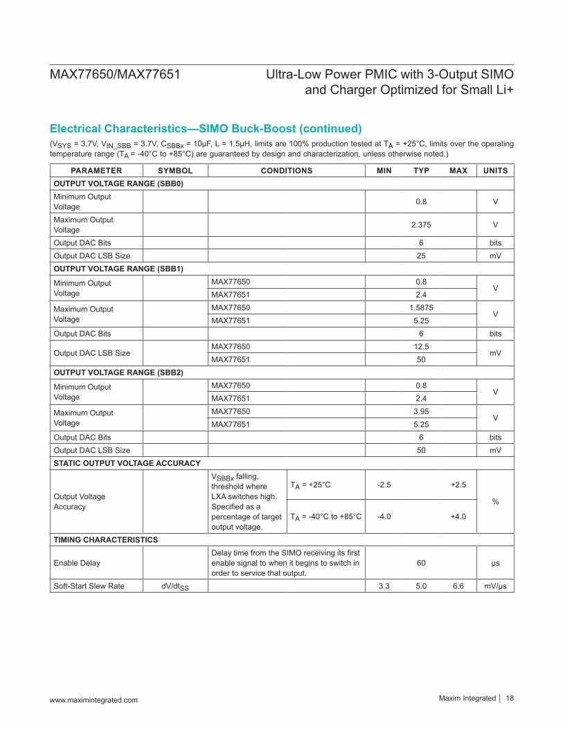
(VSYS = 3.7V, VIN_SBB = 3.7V, CSBBx = 10μF, L = 1.5μH, limits are 100% production tested at TA = +25°C, limits over the operating temperature range (TA = -40°C to +85°C) are guaranteed by design and characterization, unless otherwise noted.)
PARAMETER SYMBOL CONDITIONS MIN TYP MAX UNITSOUTPUT VOLTAGE RANGE (SBB0)Minimum Output Voltage 0.8 V
Maximum Output Voltage 2.375 V
Output DAC Bits 6 bitsOutput DAC LSB Size 25 mVOUTPUT VOLTAGE RANGE (SBB1)
Minimum Output Voltage
MAX77650 0.8V
MAX77651 2.4
Maximum Output Voltage
MAX77650 1.5875V
MAX77651 5.25Output DAC Bits 6 bits
Output DAC LSB SizeMAX77650 12.5
mVMAX77651 50
OUTPUT VOLTAGE RANGE (SBB2)
Minimum Output Voltage
MAX77650 0.8V
MAX77651 2.4
Maximum Output Voltage
MAX77650 3.95V
MAX77651 5.25Output DAC Bits 6 bitsOutput DAC LSB Size 50 mVSTATIC OUTPUT VOLTAGE ACCURACY
Output Voltage Accuracy
VSBBx falling, threshold where LXA switches high. Specified as a percentage of target output voltage.
TA = +25°C -2.5 +2.5
%
TA = -40°C to +85°C -4.0 +4.0
TIMING CHARACTERISTICS
Enable DelayDelay time from the SIMO receiving its first enable signal to when it begins to switch in order to service that output.
60 μs
Soft-Start Slew Rate dV/dtSS 3.3 5.0 6.6 mV/μs
Electrical Characteristics—SIMO Buck-Boost (continued)
www.maximintegrated.com Maxim Integrated 18
MAX77650/MAX77651 Ultra-Low Power PMIC with 3-Output SIMO and Charger Optimized for Small Li+

(VSYS = 3.7V, VIN_SBB = 3.7V, CSBBx = 10μF, L = 1.5μH, limits are 100% production tested at TA = +25°C, limits over the operating temperature range (TA = -40°C to +85°C) are guaranteed by design and characterization, unless otherwise noted.)
Note 3: Guaranteed by design and characterization but not directly production tested. Production test coverage is provided by the shutdown supply current and quiescent supply current specification in the Electrical Characteristics—Top Level table.
Note 4: Typical values align with bench observations using the stated conditions. Minimum and maximum values are tested in pro-duction with DC currents. See the Typical Operating Characteristics SIMO switching waveforms to gain more insight on this specification.
PARAMETER SYMBOL CONDITIONS MIN TYP MAX UNITSPOWER STAGE CHARACTERISTICS
LXA Leakage Current
SBB0, SBB1, SBB2 are disabled, VIN_SBB = 5.5V, VLXA = 0V, or 5.5V
TA = +25°C -1.0 ±0.1 +1.0μA
TA = +85°C ±1.0
LXB Leakage Current
SBB0, SBB1, SBB2 are disabled, VIN_SBB = 5.5V, VLXA = 0V or 5.5V, all VSBBx = 5.5V
TA = +25°C -1.0 ±0.1 +1.0
μA
TA = +85°C ±1.0
BST Leakage CurrentVIN_SBB = 5.5V, VLXB = 5.5V, VBST = 11V
TA = +25°C +0.01 +1.0μA
TA = +85°C +0.1
Disabled Output Leakage Current
SBB0, SBB1, SBB2 are disabled, active-discharge disabled (ADE_SBBx = 0), VSBBx = 5.5V, VLXB = 0V, VSYS = VIN_SBB = VBST = 5.5V
TA = +25°C +0.1 +1.0
μA
TA = +85°C +0.2
Active Discharge Impedance RAD_SBBx
SBB0, SBB1, SBB2 are disabled, active discharge enabled (ADE_SBBx = 1) 80 140 260 Ω
CONTROL SCHEME
Peak Current Limit (Note 4) IP_SBB
IP_SBBx = 0b11 0.414 0.500 0.586
AIP_SBBx = 0b10 0.589 0.707 0.806IP_SBBx = 0b01 0.713 0.866 0.947IP_SBBx = 0b00 0.892 1.000 1.108
Electrical Characteristics—SIMO Buck-Boost (continued)
www.maximintegrated.com Maxim Integrated 19
MAX77650/MAX77651 Ultra-Low Power PMIC with 3-Output SIMO and Charger Optimized for Small Li+

(VSYS = 3.7V, VIN_LDO = 2.05V, VLDO = 1.85V, CLDO = 10μF, limits are 100% production tested at TA = +25°C, limits over the operating temperature range (TA = -40°C to +85°C) are guaranteed by design and characterization, unless otherwise noted.)
PARAMETER SYMBOL CONDITIONS MIN TYP MAX UNITSGENERAL CHARACTERISTICS
Input Voltage VIN_LDOIN_LDO cannot exceed SYS voltage (Note 5) 1.8 5.5 V
LDO Shutdown Current IIN_LDOCurrent measured into IN_LDO, LDO output disabled (Note 6) 0.1 1 μA
LDO Quiescent Supply Current (Note 6) IIN_LDO
Current measured into IN_LDO, ILDO = 0mA
LDO output enabled and in regulation, VIN_LDO = 2.05V, VLDO = 1.85V
1.7 5.15
μALDO output enabled and in dropout, VIN_LDO = 1.8V, VLDO target is 1.85V
2.3
Maximum Output Current IOUT 150 mA
Current Limit VLDO externally forced to 1.3V 165 255 375 mAOUTPUT VOLTAGE RANGE
Output Voltage Range Programmable with TV_LDO[6:0] in 12.5mV steps 1.3500 2.9375 V
Output DAC Bits 7 bitsOutput DAC LSB Size 12.5 mVSTATIC CHARACTERISTICSInitial Output Voltage Accuracy ILDO = 75mA, TA = +25°C -2.5 +2.5 %
Output Voltage Accuracy
VLDO programmed from 1.35V to 2.9375V, VIN_LDO = 1.8V to 5.5V, LDO not in drop-out, ILDO = 0mA to 150mA, TA = -5°C to +85°C
-3 +3 %
Output Noise
f = 10Hz to 100kHz, IOUT = 15mA, VSYS = 3.7V, VIN_LDO = 2.05V, VLDO = 1.85V
Main bias circuits are in normal-power mode (SBIA_LPM = 0)
550
μVRMSMain bias circuits are in low-power mode (SBIA_LPM = 1)
800
Electrical Characteristics—LDO
www.maximintegrated.com Maxim Integrated 20
MAX77650/MAX77651 Ultra-Low Power PMIC with 3-Output SIMO and Charger Optimized for Small Li+

(VSYS = 3.7V, VIN_LDO = 2.05V, VLDO = 1.85V, CLDO = 10μF, limits are 100% production tested at TA = +25°C, limits over the operating temperature range (TA = -40°C to +85°C) are guaranteed by design and characterization, unless otherwise noted.)
Note 5: Dropout is the condition where the input voltage is in its valid input range but the output cannot be properly regulated because the input voltage is not sufficiently higher than the output voltage. The dropout voltage is the difference between the input voltage and the output voltage when the regulator is in dropout. The dropout on-resistance is the resistance of the power MOSFET between the input and the output when the regulator is in dropout. Generally speaking, applications should avoid dropout by having sufficient input voltage. A dropout detection interrupt is available (DOD_R; see the Programmer’s Guide for more information). For example, applications with the output voltage target of 1.85V and the maximum load cur-rent is 80mA (ILDO_MAX), has a dropout voltage of 96mV (VLDO_DO = ILDO_MAX x RDSON_LDO = 80mA x 1.2Ω = 96mV). To avoid dropout, the input voltage should be 1.95V (VIN_LDO = VLDO + VLDO_DO).
Note 6: Guaranteed by design and characterization but not directly production tested. Production test coverage is provided by the shutdown supply current and quiescent supply current specification in the Electrical Characteristics—Top Level table.
Note 7: Guaranteed by design and characterization but not directly production tested. The ability to disconnect the active discharge resistance is functionally checked in a production test.
PARAMETER SYMBOL CONDITIONS MIN TYP MAX UNITSTIMING CHARACTERISTICSEnable Delay TA = +25°C 0.6 1.25 ms
Soft-Start Slew Rate dV/dtSSVLDO from 10% to 90% of final value. TA = +25°C 0.5 1.25 2.50 mV/μs
POWER STAGE CHARACTERISTICS
Dropout Voltage VLDO_DO
VSYS = 3.7V, 1.85V programmed output voltage (TV_LDO[6:0] = 0x20), VIN_LDO = 1.8V, ILDO = 150mA (Note 5)
90 180 mV
Active-Discharge Impedance RAD_LDO
Regulator disabled, active discharge enabled (ADE_LDO = 1) 50 100 200 Ω
Disabled Output Leakage Current
Regulator disabled, active discharge disabled (ADE_LDO = 0), VSYS = VIN_LDO = 5.5V, VLDO = 5.5V and 0V
TA = +25°C (Note 7) +0.1 +1.0
μA
TA = +85°C +1.0
Dropout On-Resistance RDSON
VSYS = 3.7V, 1.85V programmed output voltage (TV_LDO[6:0] = 0x20), VIN_LDO = 1.8V, ILDO = IMAX, (Note 5)
TA = +25°C 0.6 0.9
Ω
TA = +85°C 1.2
Electrical Characteristics—LDO (continued)
www.maximintegrated.com Maxim Integrated 21
MAX77650/MAX77651 Ultra-Low Power PMIC with 3-Output SIMO and Charger Optimized for Small Li+

(VSYS = 3.7V, limits are 100% production tested at TA = +25°C, limits over the operating temperature range (TA = -40°C to +85°C) are guaranteed by design and characterization, unless otherwise noted.)
PARAMETER SYMBOL CONDITIONS MIN TYP MAX UNITSGENERAL CHARACTERISTICS
Current Sink Quiescent Current IQ
Change in supply current at SYS when one channel is enabled and delivering 12.8mA, VLEDx = 0.2V
6 12 µA
Current Sink Leakage
All current sink drivers combined, outputs disabled, VLEDx = 5.5V
TA = +25ºC +0.1 +1.0µA
TA = +85ºC +1.0
3.2mA CURRENT SINK RANGE (LED_FSx[1:0] = 0b01, VLEDx = 0.2V)Minimum Sink Current BRT_LEDx[4:0] = 0b00000 0.1 mAMaximum Sink Current BRT_LEDx[4:0] = 0b11111 3.2 mACurrent Sink DAC Bits 5 bitsCurrent Sink DAC LSB 0.1 mA
Current Sink AccuracyTA = +25ºC 3.10 3.20 3.25
mATA = -40ºC to +85ºC 3.03 3.20 3.36
Dropout Voltage VDO BRT_LEDx[4:0] = 0b11111, ILEDx = 2.9mA 35 70 mV6.4mA CURRENT SINK RANGE (LED_FSx[1:0] = 0b10, VLEDx = 0.2V)Minimum Sink Current BRT_LEDx[4:0] = 0b00000 0.2 mAMaximum Sink Current BRT_LEDx[4:0] = 0b11111 6.4 mACurrent Sink DAC Bits 5 bitsCurrent Sink DAC LSB 0.2 mA
Current Sink AccuracyTA = +25ºC 6.30 6.40 6.50
mATA = -40ºC to +85ºC 6.06 6.40 6.72
Dropout Voltage VDOLED_FSx[1:0] = 0b11, BRT_LEDx[4:0] = 0b11111, ILEDx = 5.75mA 35 70 mV
12.8mA CURRENT SINK RANGE (LED_FSx[1:0] = 0b11, VLEDx = 0.2V)Minimum Sink Current BRT_LEDx[4:0] = 0b00000 0.4 mAMaximum Sink Current BRT_LEDx[4:0] = 0b11111 12.8 mACurrent Sink DAC Bits 5 bitsCurrent Sink DAC LSB 0.4 mA
Current Sink AccuracyTA = +25ºC 12.6 12.8 13.0
mATA = -40ºC to +85ºC 12.16 12.80 13.44
Dropout Voltage VDO BRT_LEDx[4:0] = 0b11111, ILEDx = 11.5mA 35 70 mVTIMING CHARACTERISTICSRoot Clock Frequency 25.6 32.0 38.4 Hz
Electrical Characteristics—Current Sinks
www.maximintegrated.com Maxim Integrated 22
MAX77650/MAX77651 Ultra-Low Power PMIC with 3-Output SIMO and Charger Optimized for Small Li+

(VSYS = 3.7V, limits are 100% production tested at TA = +25°C, limits over the operating temperature range (TA = -40°C to +85°C) are guaranteed by design and characterization, unless otherwise noted.)
(VSYS = 3.7V, VIO = 1.8V, limits are 100% production tested at TA = +25°C, limits over the operating temperature range (TA = -40°C to +85°C) are guaranteed by design and characterization, unless otherwise noted.)
PARAMETER SYMBOL CONDITIONS MIN TYP MAX UNITSTIMING CHARACTERISTICS/BLINK PERIOD SETTINGS
Minimum Blink Period0.5 s16 clocks
Maximum Blink Period8 s
256 clocks
Blink Period LSB0.5 s16 clocks
TIMING CHARACTERISTICS/BLINK DUTY CYCLEMinimum Blink Duty Cycle D_LEDx[3:0] = 0b0000 6.25 %Maximum Blink Duty Cycle D_LEDx[3:0] = 0b1111 100 %Blink Duty Cycle LSB 6.25 %
PARAMETER SYMBOL CONDITIONS MIN TYP MAX UNITSPOWER SUPPLYVIO Voltage Range VIO 1.7 1.8 3.6 V
VIO Bias CurrentVIO = 3.6V, VSDA = VSCL = 0V or 3.6V, TA = +25°C -1 0 +1
μAVIO = 1.7V, VSDA = VSCL= 0V or 1.7V -1 0 +1
SDA AND SCL I/O STAGESCL, SDA Input High Voltage VIH VIO = 1.7V to 3.6V 0.7 x
VIOV
SCL, SDA Input Low Voltage VIL VIO = 1.7V to 3.6V 0.3 x
VIOV
SCL, SDA Input Hysteresis VHYS
0.05 x VIO
V
SCL, SDA Input Leakage Current II VIO = 3.6V, VSCL = VSDA = 0V and 3.6V -10 +10 μA
SDA Output Low Voltage VOL Sinking 20mA 0.4 V
SCL, SDA Pin Capacitance CI 10 pF
Output Fall Time from VIH to VIL (Note 2) tOF 120 ns
Electrical Characteristics—Current Sinks (continued)
Electrical Characteristics—I2C
www.maximintegrated.com Maxim Integrated 23
MAX77650/MAX77651 Ultra-Low Power PMIC with 3-Output SIMO and Charger Optimized for Small Li+

(VSYS = 3.7V, VIO = 1.8V, limits are 100% production tested at TA = +25°C, limits over the operating temperature range (TA = -40°C to +85°C) are guaranteed by design and characterization, unless otherwise noted.)
PARAMETER SYMBOL CONDITIONS MIN TYP MAX UNITSI2C-COMPATIBLE INTERFACE TIMING (STANDARD, FAST AND FAST MODE PLUS) (Note 8)Clock Frequency fSCL 0 1000 kHzHold Time (REPEATED) START Condition tHD;STA 0.26 μs
SCL Low Period tLOW 0.5 μsSCL High Period tHIGH 0.26 μsSetup Time REPEATED START Condition tSU_STA 0.26 μs
Data Hold Time tHD_DAT 0 μsData Setup Time tSU_DAT 50 nsSetup Time for STOP Condition tSU_STO 0.26 μs
Bus Free Time between STOP and START Condition
tBUF 0.5 μs
Pulse Width of Sup-pressed Spikes tSP
Maximum pulse width of spikes that must be suppressed by the input filter 50 ns
I2C-COMPATIBLE INTERFACE TIMING (HIGH-SPEED MODE, CB = 100pF) (Note 8)Clock Frequency fSCL 3.4 MHzSetup Time REPEATED START Condition tSU_STA 160 ns
Hold Time (REPEATED) START Condition tHD_STA 160 ns
SCL Low Period tLOW 160 nsSCL High Period tHIGH 60 nsData Setup Time tSU_DAT 10 nsData Hold Time tHD_DAT 0 70 nsSCL Rise Time trCL TA = +25°C 10 40 nsRise Time of SCL Signal after REPEATED START Condition and after Acknowledge Bit
trCL1 TA = +25°C 10 80 ns
SCL Fall Time tfCL TA = +25°C 10 40 nsSDA Rise Time trDA TA = +25°C 10 80 nsSDA Fall Time tfDA TA = +25°C 10 80 nsSetup Time for STOP Condition tSU_STO 160 ns
Bus Capacitance CB 100 pFPulse Width of Sup-pressed Spikes tSP
Maximum pulse width of spikes that must be suppressed by the input filter 10 ns
Electrical Characteristics—I2C (continued)
www.maximintegrated.com Maxim Integrated 24
MAX77650/MAX77651 Ultra-Low Power PMIC with 3-Output SIMO and Charger Optimized for Small Li+
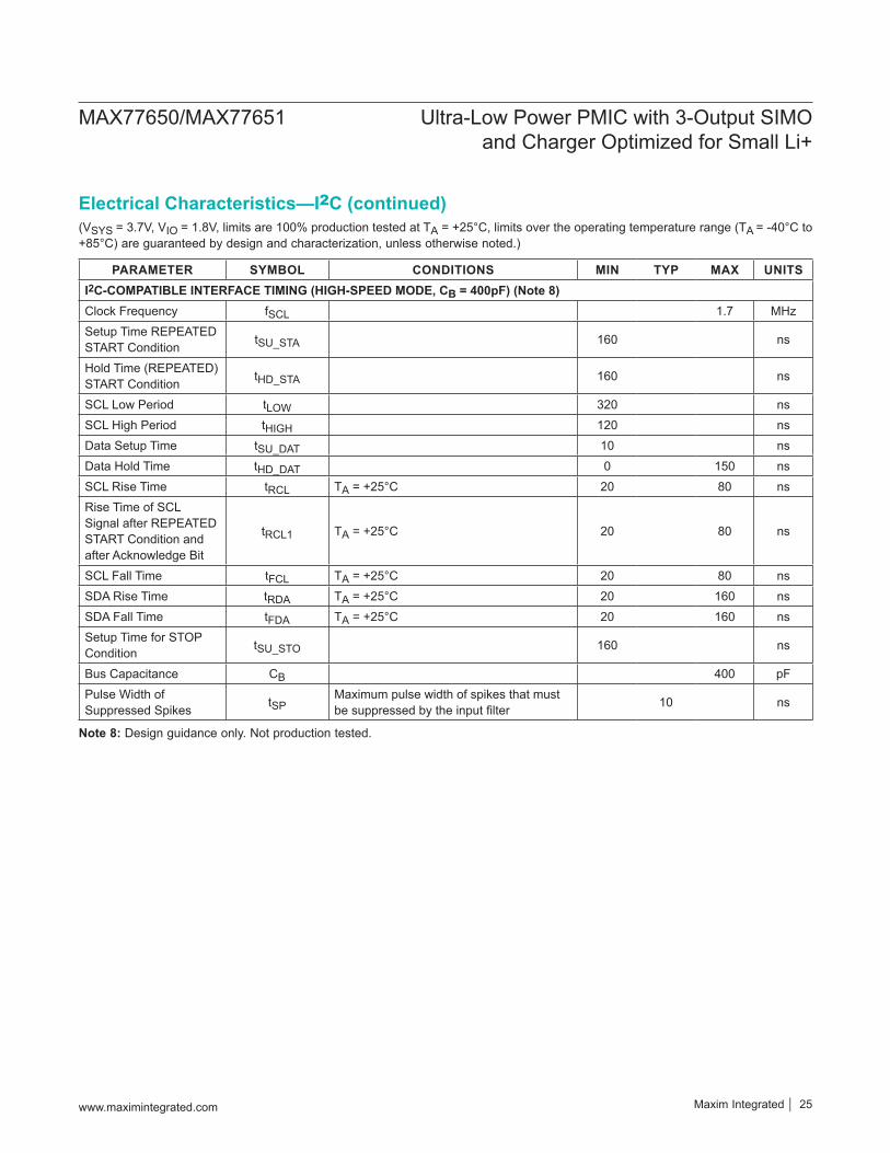
(VSYS = 3.7V, VIO = 1.8V, limits are 100% production tested at TA = +25°C, limits over the operating temperature range (TA = -40°C to +85°C) are guaranteed by design and characterization, unless otherwise noted.)
Note 8: Design guidance only. Not production tested.
PARAMETER SYMBOL CONDITIONS MIN TYP MAX UNITSI2C-COMPATIBLE INTERFACE TIMING (HIGH-SPEED MODE, CB = 400pF) (Note 8)Clock Frequency fSCL 1.7 MHzSetup Time REPEATED START Condition tSU_STA 160 ns
Hold Time (REPEATED) START Condition tHD_STA 160 ns
SCL Low Period tLOW 320 nsSCL High Period tHIGH 120 nsData Setup Time tSU_DAT 10 nsData Hold Time tHD_DAT 0 150 nsSCL Rise Time tRCL TA = +25°C 20 80 nsRise Time of SCL Signal after REPEATED START Condition and after Acknowledge Bit
tRCL1 TA = +25°C 20 80 ns
SCL Fall Time tFCL TA = +25°C 20 80 nsSDA Rise Time tRDA TA = +25°C 20 160 nsSDA Fall Time tFDA TA = +25°C 20 160 nsSetup Time for STOP Condition tSU_STO 160 ns
Bus Capacitance CB 400 pFPulse Width of Suppressed Spikes tSP
Maximum pulse width of spikes that must be suppressed by the input filter 10 ns
Electrical Characteristics—I2C (continued)
www.maximintegrated.com Maxim Integrated 25
MAX77650/MAX77651 Ultra-Low Power PMIC with 3-Output SIMO and Charger Optimized for Small Li+
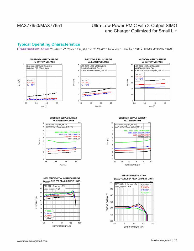
(Typical Application Circuit, VCHGIN = 0V, VSYS = VIN_SBB = 3.7V, VBATT = 3.7V, VIO = 1.8V, TA = +25°C, unless otherwise noted.)
0
1
2
3
4
5
6
2.5 3.5 4.5 5.5
I BATT
(µA)
VBATT (V)
LDO, SIMO, LED'S ARE DISABLEDMAIN-BIAS OFF (SBIA_EN = 0)
TA = +85°CTA = +25°CTA = -40°C
SHUTDOWN SUPPLY CURRENTvs. BATTERY VOLTAGE
toc 01
0
1
2
3
4
5
6
2.5 3.5 4.5 5.5
I BATT
(µA)
VBATT (V)
LDO, SIMO, LED'S ARE DISABLEDMAIN-BIAS ON (SBIA_EN = 1)LOW-POWER MODE (SBIA_LPM = 1)
TA = +85°CTA = +25°CTA = -40°C
SHUTDOWN SUPPLY CURRENTvs. BATTERY VOLTAGE
toc 02
0
10
20
30
40
50
60
2.5 3.5 4.5 5.5
I BATT
(µA)
VBATT (V)
LDO, SIMO, LED'S ARE DISABLEDMAIN-BIAS ON (SBIA_EN = 1)NORMAL-POWER MODE (SBIA_LPM = 0)
TA = +85°CTA = +25°CTA = -40°C
SHUTDOWN SUPPLY CURRENTvs. BATTERY VOLTAGE
toc 03
0
1
2
3
4
5
6
7
8
9
10
2.5 3.5 4.5 5.5
I BATT
(µA)
VBATT (V)
MAIN-BIAS ON (SBIA_EN = 1)LOW-POWER MODE (SBIA_LPM = 1)
SBB0 ENABLEDSBB0, SBB1 ENABLED
SBB0, SBB1, SBB2 ENABLEDSBB0, SBB1, SBB2, LDO ENABLED
QUIESCENT SUPPLY CURRENTvs. BATTERY VOLTAGE
toc 04
0
1
2
3
4
5
6
7
8
9
10
-40 -15 10 35 60 85
I BATT
(µA)
TEMPERATURE (°C)
SBB0 ENABLEDSBB0, SBB1 ENABLED
SBB0, SBB1, SBB2 ENABLEDSBB0, SBB1, SBB2, LDO ENABLED
MAIN-BIAS ON (SBIA_EN = 1)LOW-POWER MODE (SBIA_LPM = 1)
QUIESCENT SUPPLY CURRENTvs. TEMPERATURE
toc 05
70
72
74
76
78
80
82
84
86
88
0.1 1 10 100 1000
EFFIC
IENC
Y (%
)
OUTPUT CURRENT (mA)
DRV_SBB = 0, VIN_SBB = 3.7VCSBB2_EFFECTIVE = 3µF
IP_SBB2 = 0IP_SBB2 = 1IP_SBB2 = 2IP_SBB2 = 3
SBB2 EFFICIENCY vs. OUTPUT CURRENT (VSBB2 = 3.3V, PER PEAK CURRENT LIMIT)
toc 06
3.20
3.25
3.30
3.35
3.40
3.45
3.50
0.1 1 10 100 1000
OUTP
UT V
OLTA
GE (V
)
OUTPUT CURRENT (mA)
DRV_SBB = 0, VIN_SBB = 3.7VCSBB2_EFFECTIVE = 3µF
IP_SBB2 = 0IP_SBB2 = 1IP_SBB2 = 2IP_SBB2 = 3
SBB2 LOAD REGULATION(VSBB2 = 3.3V, PER PEAK CURRENT LIMIT)
toc 07
Typical Operating Characteristics
www.maximintegrated.com Maxim Integrated 26
MAX77650/MAX77651 Ultra-Low Power PMIC with 3-Output SIMO and Charger Optimized for Small Li+
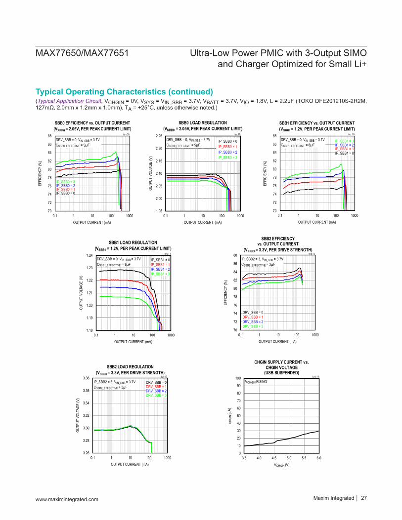
(Typical Application Circuit, VCHGIN = 0V, VSYS = VIN_SBB = 3.7V, VBATT = 3.7V, VIO = 1.8V, L = 2.2µF (TOKO DFE201210S-2R2M, 127mΩ, 2.0mm x 1.2mm x 1.0mm), TA = +25°C, unless otherwise noted.)
70
72
74
76
78
80
82
84
86
88
0.1 1 10 100 1000
EFFI
CIEN
CY (%
)
OUTPUT CURRENT (mA)
DRV_SBB = 0, VIN_SBB = 3.7VCSBB0_EFFECTIVE = 5µF
IP_SBB0 = 0IP_SBB0 = 1IP_SBB0 = 2IP_SBB0 = 3
SBB0 EFFICIENCY vs. OUTPUT CURRENT (VSBB0 = 2.05V, PER PEAK CURRENT LIMIT)
toc08
1.95
2.00
2.05
2.10
2.15
2.20
2.25
0.1 1 10 100 1000
OUTP
UT V
OLTA
GE (V
)
OUTPUT CURRENT (mA)
DRV_SBB = 0, VIN_SBB = 3.7VCSBB0_EFFECTIVE = 5µF
IP_SBB0 = 0IP_SBB0 = 1IP_SBB0 = 2IP_SBB0 = 3
SBB0 LOAD REGULATION(VSBB0 = 2.05V, PER PEAK CURRENT LIMIT)
toc 09
70
72
74
76
78
80
82
84
86
88
0.1 1 10 100 1000
EFFI
CIEN
CY (%
)
OUTPUT CURRENT (mA)
DRV_SBB = 0, VIN_SBB = 3.7VCSBB1_EFFECTIVE = 8µF
IP_SBB1 = 0IP_SBB1 = 1IP_SBB1 = 2IP_SBB1 = 3
SBB1 EFFICIENCY vs. OUTPUT CURRENT(VSBB1 = 1.2V, PER PEAK CURRENT LIMIT)
toc10
1.18
1.19
1.20
1.21
1.22
1.23
1.24
0.1 1 10 100 1000
OUTP
UT V
OLTA
GE (V
)
OUTPUT CURRENT (mA)
DRV_SBB = 0, VIN_SBB = 3.7VCSBB1_EFFECTIVE = 8µF
IP_SBB1 = 0IP_SBB1 = 1IP_SBB1 = 2IP_SBB1 = 3
SBB1 LOAD REGULATION(VSBB1 = 1.2V, PER PEAK CURRENT LIMIT)
toc 11
70
72
74
76
78
80
82
84
86
88
0.1 1 10 100 1000
EFFI
CIEN
CY (%
)
OUTPUT CURRENT (mA)
IP_SBB2 = 3, VIN_SBB = 3.7VCSBB2_EFFECTIVE = 3µF
DRV_SBB = 0DRV_SBB = 1DRV_SBB = 2DRV_SBB = 3
SBB2 EFFICIENCYvs. OUTPUT CURRENT
(VSBB2 = 3.3V, PER DRIVE STRENGTH)toc12
3.26
3.28
3.30
3.32
3.34
3.36
3.38
0.1 1 10 100 1000
OUTP
UT V
OLTA
GE (V
)
OUTPUT CURRENT (mA)
IP_SBB2 = 3, VIN_SBB = 3.7VCSBB2_EFFECTIVE = 3µF
DRV_SBB = 0DRV_SBB = 1DRV_SBB = 2DRV_SBB = 3
SBB2 LOAD REGULATION(VSBB2 = 3.3V, PER DRIVE STRENGTH)
toc13
0
10
20
30
40
50
60
70
80
90
100
3.5 4.0 4.5 5.0 5.5 6.0
I CHGI
N(µ
A)
VCHGIN (V)
VCHGIN RISING
CHGIN SUPPLY CURRENT vs.CHGIN VOLTAGE
(USB SUSPENDED)toc 14
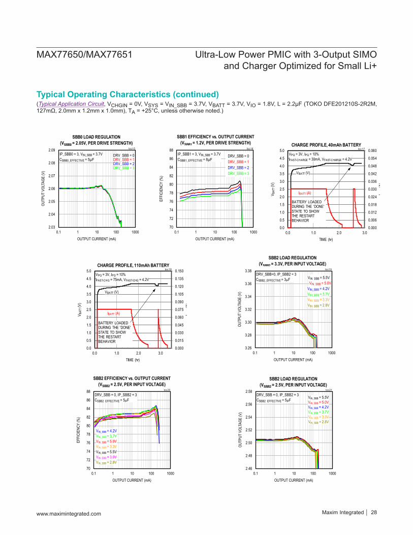
Typical Operating Characteristics (continued)
Maxim Integrated 27www.maximintegrated.com
MAX77650/MAX77651 Ultra-Low Power PMIC with 3-Output SIMO and Charger Optimized for Small Li+
2.03
2.04
2.05
2.06
2.07
2.08
2.09
0.1 1 10 100 1000
OUTP
UT V
OLTA
GE (V
)
OUTPUT CURRENT (mA)
IP_SBB0 = 3, VIN_SBB = 3.7VCSBB0_EFFECTIVE = 5µF
DRV_SBB = 0DRV_SBB = 1DRV_SBB = 2DRV_SBB = 3
SBB0 LOAD REGULATION(VSBB0 = 2.05V, PER DRIVE STRENGTH)
toc15
70
72
74
76
78
80
82
84
86
88
0.1 1 10 100 1000
EFFI
CIEN
CY (%
)
OUTPUT CURRENT (mA)
IP_SBB1 = 3, VIN_SBB = 3.7VCSBB1_EFFECTIVE = 8µF
DRV_SBB = 0DRV_SBB = 1DRV_SBB = 2DRV_SBB = 3
SBB1 EFFICIENCY vs. OUTPUT CURRENT (VSBB1 = 1.2V, PER DRIVE STRENGTH)
toc16
0.000
0.006
0.012
0.018
0.024
0.030
0.036
0.042
0.048
0.054
0.060
0.0
0.5
1.0
1.5
2.0
2.5
3.0
3.5
4.0
4.5
5.0
0.0 1.0 2.0 3.0
I BATT
(A)
V BAT
T(V
)
TIME (hr)
VPQ = 3V, IPQ = 10%IFAST-CHARGE = 30mA, VFAST-CHARGE = 4.2V
VBATT (V)
IBATT (A)
CHARGE PROFILE, 40mAh BATTERYtoc 17
BATTERY LOADED DURING THE 'DONE' STATE TO SHOW THE RESTART BEHAVIOR
0.000
0.015
0.030
0.045
0.060
0.075
0.090
0.105
0.120
0.135
0.150
0.0
0.5
1.0
1.5
2.0
2.5
3.0
3.5
4.0
4.5
5.0
0.0 1.0 2.0 3.0
I BATT
(A)
V BAT
T(V
)
TIME (hr)
VPQ = 3V, IPQ = 10%IFAST-CHG = 75mA, VFAST-CHG = 4.2V
VBATT (V)
IBATT (A)
CHARGE PROFILE, 110mAh BATTERYtoc 18
BATTERY LOADED DURING THE 'DONE' STATE TO SHOW THE RESTART BEHAVIOR
70
72
74
76
78
80
82
84
86
88
0.1 1 10 100 1000
EFFI
CIEN
CY (%
)
OUTPUT CURRENT (mA)
VIN_SBB = 5.5V
VIN_SBB = 5.0V
VIN_SBB = 4.2VVIN_SBB = 3.7V
VIN_SBB = 3.3V
VIN_SBB = 3.0VVIN_SBB = 2.8V
DRV_SBB = 0, IP_SBB2 = 3CSBB2_EFFECTIVE = 5µF
SBB2 EFFICIENCY vs. OUTPUT CURRENT (VSBB2 = 2.5V, PER INPUT VOLTAGE)
toc20
3.26
3.28
3.30
3.32
3.34
3.36
3.38
0.1 1 10 100 1000
OUTP
UT V
OLTA
GE (V
)
OUTPUT CURRENT (mA)
DRV_SBB=0, IP_SBB2 = 3CSBB2_EFFECTIVE = 3µF VIN_SBB = 5.5V
VIN_SBB = 5.0VVIN_SBB = 4.2VVIN_SBB = 3.7VVIN_SBB = 3.3VVIN_SBB = 2.8V
SBB2 LOAD REGULATION(VSBB2 = 3.3V, PER INPUT VOLTAGE)
toc19
2.46
2.48
2.50
2.52
2.54
2.56
2.58
0.1 1 10 100 1000
OUTP
UT V
OLTA
GE (V
)
OUTPUT CURRENT (mA)
DRV_SBB = 0, IP_SBB2 = 3CSBB2_EFFECTIVE = 5µF VIN_SBB = 5.5V
VIN_SBB = 5.0VVIN_SBB = 4.2VVIN_SBB = 3.7VVIN_SBB = 3.3VVIN_SBB = 2.8V
SBB2 LOAD REGULATION(VSBB2 = 2.5V, PER INPUT VOLTAGE)
toc21
Typical Operating Characteristics (continued)(Typical Application Circuit, VCHGIN = 0V, VSYS = VIN_SBB = 3.7V, VBATT = 3.7V, VIO = 1.8V, L = 2.2µF (TOKO DFE201210S-2R2M, 127mΩ, 2.0mm x 1.2mm x 1.0mm), TA = +25°C, unless otherwise noted.)
Maxim Integrated 28www.maximintegrated.com
MAX77650/MAX77651 Ultra-Low Power PMIC with 3-Output SIMO and Charger Optimized for Small Li+

(Typical Application Circuit, VCHGIN = 0V, VSYS = VIN_SBB = 3.7V, VBATT = 3.7V, VIO = 1.8V, L = 2.2µF (TOKO DFE201210S-2R2M, 127mΩ, 2.0mm x 1.2mm x 1.0mm), TA = +25°C, unless otherwise noted.)
70
72
74
76
78
80
82
84
86
88
0.1 1 10 100 1000
EFFI
CIEN
CY (%
)
OUTPUT CURRENT (mA)
DRV_SBB = 0, IP_SBB0 = 3CSBB0_EFFECTIVE = 5µF
VIN_SBB = 5.5VVIN_SBB = 5.0V
VIN_SBB = 4.2V
VIN_SBB = 3.7VVIN_SBB = 3.3V
VIN_SBB = 3.0VVIN_SBB = 2.8V
SBB0 EFFICIENCY vs. OUTPUT CURRENT(VSBB0 = 2.05V, PER INPUT VOLTAGE)
toc22
70
72
74
76
78
80
82
84
86
88
0.1 1 10 100 1000
EFFI
CIEN
CY (%
)
OUTPUT CURRENT (mA)
DRV_SBB = 0, IP_SBB0 = 3CSBB0_EFFECTIVE = 5µF
VIN_SBB = 5.5VVIN_SBB = 5.0V
VIN_SBB = 4.2V
VIN_SBB = 3.7VVIN_SBB = 3.3V
VIN_SBB = 3.0VVIN_SBB = 2.8V
SBB0 EFFICIENCY vs. OUTPUT CURRENT (VSBB0 = 1.85V, PER INPUT VOLTAGE)
toc24
2.03
2.04
2.05
2.06
2.07
2.08
2.09
0.1 1 10 100 1000OU
TPUT
VOL
TAGE
(V)
OUTPUT CURRENT (mA)
DRV_SBB = 0, IP_SBB0 = 3CSBB0_EFFECTIVE = 5µF
VIN_SBB = 5.5VVIN_SBB = 5.0VVIN_SBB = 4.2VVIN_SBB = 3.7VVIN_SBB = 3.3VVIN_SBB = 3.0VVIN_SBB = 2.8V
SBB0 LOAD REGULATION(VSBB0 = 2.05V, PER INPUT VOLTAGE)
toc23
1.83
1.84
1.85
1.86
1.87
1.88
1.89
0.1 1 10 100 1000
OUTP
UT V
OLTA
GE (V
)
OUTPUT CURRENT (mA)
DRV_SBB = 0, IP_SBB0 = 3CSBB0_EFFECTIVE = 5µF
VIN_SBB = 5.5VVIN_SBB = 5.0VVIN_SBB = 4.2VVIN_SBB = 3.7VVIN_SBB = 3.3VVIN_SBB = 2.8V
SBB0 LOAD REGULATION(VSBB0 = 1.85V, PER INPUT VOLTAGE)
toc25
70
72
74
76
78
80
82
84
86
88
0.1 1 10 100 1000
EFFI
CIEN
CY (%
)
OUTPUT CURRENT (mA)
DRV_SBB = 0, IP_SBB0 = 3CSBB0_EFFECTIVE = 6µF
VIN_SBB = 5.5VVIN_SBB = 5.0V
VIN_SBB = 3.0VVIN_SBB = 2.8V
SBB0 EFFICIENCY vs. OUTPUT CURRENT (VSBB0 = 1.5V, PER INPUT VOLTAGE)
toc26
VIN_SBB = 4.2VVIN_SBB = 3.3VVIN_SBB = 3.7V
1.48
1.49
1.50
1.51
1.52
1.53
1.54
0.1 1 10 100 1000
OUTP
UT V
OLTA
GE (V
)
OUTPUT CURRENT (mA)
DRV_SBB = 0, IP_SBB0 = 3CSBB0_EFFECTIVE = 6µF
VIN_SBB = 5.5VVIN_SBB = 5.0VVIN_SBB = 4.2VVIN_SBB = 3.7VVIN_SBB = 3.3VVIN_SBB = 2.8V
SBB0 LOAD REGULATION(VSBB0 = 1.5V, PER INPUT VOLTAGE)
toc27
Typical Operating Characteristics (continued)
Maxim Integrated 29www.maximintegrated.com
MAX77650/MAX77651 Ultra-Low Power PMIC with 3-Output SIMO and Charger Optimized for Small Li+

(Typical Application Circuit, VCHGIN = 0V, VSYS = VIN_SBB = 3.7V, VBATT = 3.7V, VIO = 1.8V, L = 2.2µF (TOKO DFE201210S-2R2M, 127mΩ, 2.0mm x 1.2mm x 1.0mm), TA = +25°C, unless otherwise noted.)
70
72
74
76
78
80
82
84
86
88
0.1 1 10 100 1000
EFFI
CIEN
CY (%
)
OUTPUT CURRENT (mA)
VIN_SBB = 5.5VVIN_SBB = 5.0VVIN_SBB = 2.8VVIN_SBB = 3.0V
DRV_SBB = 0, IP_SBB1 = 3CSBB1_EFFECTIVE = 8µF
VIN_SBB = 4.2VVIN_SBB = 3.3V
SBB1 EFFICIENCY vs. OUTPUT CURRENT (VSBB1 = 1.2V, PER INPUT VOLTAGE)
toc28
VIN_SBB = 3.7V
70
72
74
76
78
80
82
84
86
88
0.1 1 10 100 1000
EFFI
CIEN
CY (%
)
OUTPUT CURRENT (mA)
DRV_SBB = 0, IP_SBB1 = 3CSBB1_EFFECTIVE = 8µF
VIN_SBB = 5.5VVIN_SBB = 5.0V
VIN_SBB = 4.2V
VIN_SBB = 3.7VVIN_SBB = 3.3V
VIN_SBB = 3.0VVIN_SBB = 2.8V
SBB1 EFFICIENCY vs. OUTPUT CURRENT (VSBB1 = 1.0V, PER INPUT VOLTAGE)
toc30
70
72
74
76
78
80
82
84
86
88
0.1 1 10 100 1000
EFFI
CIEN
CY (%
)
OUTPUT CURRENT (mA)
VIN_SBB = 5.5VVIN_SBB = 5.0VVIN_SBB = 2.8VVIN_SBB = 3.0VVIN_SBB = 4.2VVIN_SBB = 3.3V
DRV_SBB = 0, IP_SBB1 = 3CSBB1_EFFECTIVE = 9µF
VIN_SBB = 3.7V
SBB1 EFFICIENCY vs. OUTPUT CURRENT(VSBB1 = 0.8V, PER INPUT VOLTAGE)
toc32
1.18
1.19
1.20
1.21
1.22
1.23
1.24
0.1 1 10 100 1000OU
TPUT
VOL
TAGE
(V)
OUTPUT CURRENT (mA)
DRV_SBB = 0, IP_SBB1 = 3CSBB1_EFFECTIVE = 8µF
VIN_SBB = 5.5VVIN_SBB = 5.0VVIN_SBB = 4.2VVIN_SBB = 3.7VVIN_SBB = 3.3VVIN_SBB = 2.8V
SBB1 LOAD REGULATION(VSBB1 = 1.2V, PER INPUT VOLTAGE)
toc29
0.98
0.99
1.00
1.01
1.02
1.03
1.04
0.1 1 10 100 1000
OUTP
UT V
OLTA
GE (V
)
OUTPUT CURRENT (mA)
VIN_SBB = 2.8VVIN_SBB = 3.3VVIN_SBB = 3.7VVIN_SBB = 4.2VVIN_SBB = 5.0V
DRV_SBB = 0, IP_SBB1 = 3CSBB1_EFFECTIVE = 8µF
VIN_SBB = 5.5V
SBB1 LOAD REGULATION(VSBB1 = 1.0V, PER INPUT VOLTAGE)
toc31
0.78
0.79
0.80
0.81
0.82
0.83
0.84
0.1 1 10 100 1000
OUTP
UT V
OLTA
GE (V
)
OUTPUT CURRENT (mA)
DRV_SBB = 0, IP_SBB1 = 3CSBB1_EFFECTIVE = 9µF
VIN_SBB = 5.5VVIN_SBB = 5.0VVIN_SBB = 4.2VVIN_SBB = 3.7VVIN_SBB = 3.3VVIN_SBB = 2.8V
SBB1 LOAD REGULATION(VSBB1 = 0.8V, PER INPUT VOLTAGE)
toc33
Typical Operating Characteristics (continued)
Maxim Integrated 30www.maximintegrated.com
MAX77650/MAX77651 Ultra-Low Power PMIC with 3-Output SIMO and Charger Optimized for Small Li+

(Typical Application Circuit, VCHGIN = 0V, VSYS = VIN_SBB = 3.7V, VBATT = 3.7V, VIO = 1.8V, L = 1.5µF, TA = +25°C, unless otherwise noted.)
1V/div
50mV/div
toc 34
10µs/div
VOUTN
VINSIDE
VBACKUP
SIMO LINE TRANSIENT
VSBB2
VSBB1
VSBB0
VIN_SBB
50mV/div
50mV/div
3.2V
4.2V
IP_SBB0 = 707mA, VSBB0 = 2.05V, CSBB0_EFF = 5µFIP_SBB1 = 500mA, VSBB1 = 1.2V, CSBB1_EFF = 8µFIP_SBB2 = 866mA, VSBB2 = 3.3V, CSBB2_EFF = 6µF
L=2.2µH ISBB0 = ISBB1 = ISBB2 = 10mA
100mA/div
50mV/div
toc 36
40µs/div
SBB1 LOAD TRANSIENT
VSBB2
VSBB1
VSBB0
ISBB1
50mV/div
50mV/div
3.3V
2.05V
1.2V
10mA
100mA
ISBB0 = 10mA
ISBB2 = 10mA
IP_SBBx SET TO 500mALOW-POWER MODE
CSBB0_EFF = 5µF
CSBB1_EFF = 8µF
CSBB2_EFF = 6µF
50mV/div
500mA/div
toc 38
4µs/div
SIMO SWITCHING WAVEFORMSLIGHT UTILIZATION 10mA PER CHANNEL
VSBB2
VSBB1
VSBB0
IL
50mV/div
50mV/div
IP_SBB2 = 500mA, VSBB2 = 3.3V, CSBB2_EFF = 3µF
IP_SBB1 = 500mA, VSBB1 = 1.2V, CSBB1_EFF = 8µF
IP_SBB2 = 500mA, VSBB0 = 2.05V, CSBB0_EFF = 5µF
100mA/div
50mV/div
toc 35
40µs/div
SBB2 LOAD TRANSIENT
VSBB2
VSBB1
VSBB0
ISBB2
50mV/div
50mV/div
3.3V
2.05V
1.2V
10mA80mA
ISBB0 = 10mA
ISBB1 = 10mA
IP_SBBx SET TO 500mALOW-POWER MODE
CSBB0_EFF = 5µF
CSBB1_EFF = 8µF
CSBB2_EFF = 6µF
100mA/div
50mV/div
toc 37
40µs/div
SBB0 LOAD TRANSIENT
VSBB2
VSBB1
VSBB0
ISBB0
50mV/div
50mV/div
3.3V
2.05V
1.2V
10mA
100mA
ISBB1 = 10mA
ISBB2 = 10mA
IP_SBBx SET TO 500mALOW-POWER MODE
CSBB0_EFF = 5µF
CSBB1_EFF = 8µF
CSBB2_EFF = 6µF
50mV/div
500mA/div
toc 39
4µs/div
SIMO SWITCHING WAVEFORMSMEDIUM UTILIZATION 25mA PER CHANNEL
VSBB2
VSBB1
VSBB0
IL
50mV/div
50mV/div
IP_SBB2 = 866mA, VSBB2= 3.3V, CSBB2_EFF = 3µF
IP_SBB1 = 500mA, VSBB1 = 1.2V, CSBB1_EFF =8µF
IP_SBB2 = 707mA, VSBB0= 2.05V, CSBB0_EFF = 5µF50mV/div
500mA/div
toc 40
4µs/div
SIMO SWITCHING WAVEFORMSHEAVY UTILIZATION 75mA PER CHANNEL
VSBB2
VSBB1
VSBB0
IL
50mV/div
50mV/div
IP_SBB2 = 1000mA, VSBB2= 3.3V, CSBB2_EFF =3µF
IP_SBB1 = 1000mA, VSBB1= 1.2V, CSBB1_EFF = 8µF
IP_SBB2 = 1000mA, VSBB0= 2.05V, CSBB0_EFF =5µF
Typical Operating Characteristics (continued)
Maxim Integrated 31www.maximintegrated.com
MAX77650/MAX77651 Ultra-Low Power PMIC with 3-Output SIMO and Charger Optimized for Small Li+

(Typical Application Circuit, VCHGIN = 0V, VSYS = VIN_SBB = 3.7V, VBATT = 3.7V, VIO = 1.8V, L = 1.5µF, TA = +25°C, unless otherwise noted.)
toc 46
100µs/div
LDO LOAD TRANSIENT
VLDO
ILDO
50mV/div
50mV/div
150mA
1.85V
2mA
1.75
1.77
1.79
1.81
1.83
1.85
1.87
1.89
1.91
1.93
1.95
3.0 4.0 5.0 6.0
V LDO
(V)
VIN_LDO (V)
NO LOADTA= +25°CTA= +85°C
TA= -20°C
LDO LINE REGULATIONtoc42
toc 44
100µs/div
LDO LOAD TRANSIENT
VLDO
ILDO
50mV/div
50mV/div
80mA
1.85V
5mA
1.75
1.77
1.79
1.81
1.83
1.85
1.87
1.89
1.91
1.93
1.95
0.000 0.025 0.050 0.075 0.100 0.125 0.150
V LDO
(V)
ILDO (A)
VLDO TARGET VOLTAGE = 1.85V
5.5 VIN_LDO
3.0 VIN_LDO4.2 VIN_LDO
LDO LOAD REGULATIONtoc41
0
10
20
30
40
50
60
0.1 1 10 100 1000
PSRR
(dB)
INPUT FREQUENCY (kHz)
LDO POWER-SUPPLYREJECTION RATIO
toc 47
VIN_LDO AVERAGE = 2.05VVLDO AVERAGE = 1.85V
LOAD = 15mA
toc 43
200µs/div
LDO LINE TRANSIENT
VIN_LDO
VLDO
200mV/div
1mV/div
2.05V
2.35V
toc 45
100µs/div
LDO LOAD TRANSIENT
VLDO
ILDO
50mV/div
50mV/div
135mA
1.85V
15mA
Typical Operating Characteristics (continued)
Maxim Integrated 32www.maximintegrated.com
MAX77650/MAX77651 Ultra-Low Power PMIC with 3-Output SIMO and Charger Optimized for Small Li+

(Typical Application Circuit, VCHGIN = 0V, VSYS = VIN_SBB = 3.7V, VBATT = 3.7V, VIO = 1.8V, L = 1.5µF, TA = +25°C, unless otherwise noted.)
0.0
0.2
0.4
0.6
0.8
1.0
1.2
1.4
1.6
1.8
3.5 4.0 4.5 5.0 5.5 6.0 6.5 7.0 7.5 8.0 8.5
I CHGI
N(m
A)
VCHGIN (V)
VBATT = 2.7VVBATT = 3.6VVBATT = 4.4V
ISYS = 0mAVCHGIN RISING
CHGIN SUPPLY CURRENTvs. CHGIN VOLTAGE
toc48
0
1
2
3
4
5
6
7
8
9
10
2.5 3.0 3.5 4.0 4.5
I BATT
(µA)
VBATT (V)
CHARGER DISABLEDVCHGIN = 5V
TA = +25°CTA = -40°C
TA = +85°C
BATT BIAS CURRENT vs. BATT toc 50
0.000
0.005
0.010
0.015
0.020
0.025
0.030
0.035
0.040
0.045
0.050
2.5
2.7
2.9
3.1
3.3
3.5
3.7
3.9
4.1
4.3
4.5
0.0 0.5 1.0 1.5 2.0 2.5
I BATT
(A)
V BAT
T(V
)
TIME (hr)
VPQ = 3V, IPQ = 10%IFAST-CHARGE = 30mA, VFAST-CHARGE = 4.2V
VBATT (V)
IBATT (A)
CHARGE PROFILE, 40mAh BATTERYtoc52
0
10
20
30
40
50
60
70
80
90
100
3.5 4.0 4.5 5.0 5.5 6.0I CH
GIN
(µA)
VCHGIN (V)
VCHGIN RISING
CHGIN SUPPLY CURRENTvs. CHGIN VOLTAGE
toc 49
0.08
0.09
0.10
0.11
0.12
0.13
0.14
0.15
0.16
2.5 3.0 3.5 4.0 4.5 5.0
R DS-
ON(Ω
)
VBATT (V)
SYS TO BATT IMPEDANCEtoc 51
IBATT = 10mAIBATT = 100mAIBATT = 300mA
0.000
0.015
0.030
0.045
0.060
0.075
0.090
0.105
0.120
0.135
0.150
2.5
2.7
2.9
3.1
3.3
3.5
3.7
3.9
4.1
4.3
4.5
0.0 0.5 1.0 1.5 2.0 2.5
I BATT
(A)
V BAT
T(V
)
TIME (hr)
VPQ = 3V, IPQ = 10%IFAST-CHG = 90mA, VFAST-CHG = 4.2V
VBATT (V)
IBATT (A)
CHARGE PROFILE, 110mAh BATTERYtoc53
BATTERY LOADED DURING THE "DONE" STATE TO SHOW THE RESTARTBEHAVIOR
toc54
1ms/div
SYS LOAD TRANSIENTCAUSING BATTERY SUPPLEMENT
VSYS
IBATT
1V/div
95mA
0mA 30mA
30mA CHARGING
125mA
0mA
30mA DISCHARGING0mA
4.5V
3.7V
100mA/div
100mA/div
100mA/div
ISYS
ICHGIN
ICHGIN_LIM = 95mAICHGIN = 30mA
VSYS_REG = 4.5V
Typical Operating Characteristics (continued)
Maxim Integrated 33www.maximintegrated.com
MAX77650/MAX77651 Ultra-Low Power PMIC with 3-Output SIMO and Charger Optimized for Small Li+

(Typical Application Circuit, VCHGIN = 0V, VSYS = VIN_SBB = 3.7V, VBATT = 3.7V, VIO = 1.8V, L = 1.5µF, TA = +25°C, unless otherwise noted.)
toc57
2ms/div
POWER UP10mA LOAD PER CHANNEL
1V/div
50mA/div
1V/div1V/div
1V/div
2V/divVnRST
IBATT
VSBB2
VSBB0
VLDOVSBB1
toc55
2ms/div
POWER UPNO LOAD
1V/div
50mA/div
1V/div1V/div
1V/div
2V/divVnRST
IBATT
VSBB2
VSBB0
VLDOVSBB1
toc58
4ms/div
POWER DOWN10mA LOAD PER CHANNEL
1V/div
50mA/div
1V/div1V/div
1V/div
2V/divVnRST
IBATT
VSBB2
VSBB0
VLDOVSBB1
toc56
4ms/div
POWER DOWNNO LOAD
1V/div
50mA/div
1V/div1V/div
1V/div
2V/divVnRST
IBATT
VSBB2
VSBB0
VLDOVSBB1
Typical Operating Characteristics (continued)
Maxim Integrated 34www.maximintegrated.com
MAX77650/MAX77651 Ultra-Low Power PMIC with 3-Output SIMO and Charger Optimized for Small Li+

PIN NAME FUNCTION TYPETOP LEVEL
A2 nEN Active-Low Enable Input. nEN supports pushbutton or slide-switch configurations. digital input
C2 nIRQ Active-Low, Open-Drain Interrupt Output. Connect a 100kΩ pullup resistor between nIRQ and a voltage equal to or less than VSYS. digital output
B2 nRST Active-Low, Open-Drain Reset Output. Connect a 100kΩ pullup resistor between nRST and a voltage equal to or less than VSYS. digital output
A1 PWR_HLDActive-High Power Hold Input. Assert PWR_HLD to keep the on/off controller in its on through on/off controller state. If PWR_HLD is not needed, connect it to SYS and use the SFT_RST bits to power down the device.
digital input
B1 GPIO General-Purpose Input/Output. The GPIO I/O stage is internally biased with VIO. digital I/OC4 VIO I2C Interface and GPIO Driver Power power inputB4 SCL I2C Clock digital inputA3 SDA I2C Data digital I/O
C3 GND Quiet Ground. Connect GND to PGND, LGND, and the low-impedance ground plane of the PCB. ground
Pin Configuration
TOP VIEW(BUMP SIDE DOWN)
A
B
C
D
WLP(2.75mm x 2.15mm)
E
PWR_HLD
1
+
nEN
2
SDA
3
LED2 LED1 LED0
GPIO nRST LGND SCL LDO IN_LDO
AMUX nIRQ GND VIO BST SBB0
VL THM TBIAS LXA LXB SBB1
CHGIN SYS BATT IN_SBB PGND SBB2
4 5 6
Pin Description
www.maximintegrated.com Maxim Integrated 35
MAX77650/MAX77651 Ultra-Low Power PMIC with 3-Output SIMO and Charger Optimized for Small Li+

PIN NAME FUNCTION TYPECHARGER
E1 CHGIN Charger Input. Connect to a DC charging source. Bypass to GND with a 4.7μF ceramic capacitor. power input
E2 SYSSystem Power Output. SYS provides power to the system resources as well as the control logic of the device. Connect SYS to IN_SBB and bypass to GND with a 22μF ceramic capacitor. power output
E3 BATT Li+ Battery Connection. Connect to positive battery terminal. Bypass to GND with a 4.7μF ceramic capacitor. power I/O
D1 VL Internal Charger 3V Logic Supply Powered from CHGIN. Bypass to GND with a 1μF ceramic capacitor. Do not load VL externally. power
D3 TBIAS Thermistor Bias Supply. Connect a resistor equal to the NTC's room temperature resistance between TBIAS and THM. Do not load TBIAS with any other external circuitry. analog
D2 THM Thermistor Monitor. Thermally couple an NTC to the battery and connect between THM and GND. analog input
C1 AMUX Analog Multiplexer Output. Connect to system ADC to perform conversions on charger power signals. analog output
LDOB5 LDO Linear Regulator Output power outputB6 IN_LDO Linear Regulator Input power input
RGB LED DRIVER
A6 LED0 Current Sink Port 0. LED0 is typically connected to the cathode of an LED and is capable of sinking up to 12.5mA. Connect to ground if unused. power
A5 LED1 Current Sink Port 1. LED1 is typically connected to the cathode of an LED and is capable of sinking up to 12.5mA. Connect to ground if unused. power
A4 LED2 Current Sink Port 2. LED2 is typically connected to the cathode of an LED and is capable of sinking up to 12.5mA. Connect to ground if unused. power
B3 LGND Current Sink Ground. Connect LGND to GND, PGND, and the low-impedance ground plane of the PCB. ground
SIMO BUCK BOOST
E4 IN_SBB SIMO Power Input. Connect IN_SBB to SYS and bypass to PGND with a 10uF ceramic capacitor as close as possible to the IN_SBB pin. power input
C6 SBB0 SIMO Buck-Boost Output 0. SBB0 is the power output for channel 0 of the SIMO buck-boost. Bypass SBB0 to PGND with a 10μF ceramic capacitor. power output
D6 SBB1 SIMO Buck-Boost Output 1. SBB1 is the power output for channel 1 of the SIMO buck-boost. Bypass SBB1 to PGND with a 10μF ceramic capacitor. power output
E6 SBB2 SIMO Buck-Boost Output 2. SBB2 is the power output for channel 2 of the SIMO buck-boost. Bypass SBB2 to PGND with a 10μF ceramic capacitor. power output
C5 BST SIMO Power Input for the High-Side Output NMOS Drivers. Connect a 3300pF ceramic capaci-tor between BST and LXB. power input
D4 LXASwitching Node A. LXA is driven between PGND and IN_SBB when any SIMO channel is en-abled. LXA is driven to PGND when all SIMO channels are disabled. Connect a 1.5μH inductor between LXA and LXB.
power I/O
D5 LXBSwitching Node B. LXB is driven between PGND and SBBx when SBBx is enabled. LXB is driven to PGND when all SIMO channels are disabled. Connect a 1.5μH inductor between LXA and LXB.
power I/O
E5 PGND Power ground for the SIMO low-side FETs. Connect PGND to GND, LGND, and the low-imped-ance ground plane of the PCB. ground
Pin Description (continued)
www.maximintegrated.com Maxim Integrated 36
MAX77650/MAX77651 Ultra-Low Power PMIC with 3-Output SIMO and Charger Optimized for Small Li+

Detailed DescriptionThe MAX77650/MAX77651 provide a highly-integrated battery charging and power management solution for low-power applications. The linear charger provides a wide range of charge current and charger termination voltage options to charge various Li+ batteries. Temperature monitoring and JEITA compliance settings add additional functionality and safety to the charger. Four regulators are integrated within this device (see Table 1). A single-inductor, multiple output (SIMO) buck-boost regulator efficiently provides three independently programmable power rails. A 150mA LDO provides ripple rejection for audio and other low-noise applications.The system includes other features such as current sinks for driving LED indicators and an analog multiplexer that switches several internal voltage and current signals to an external node for monitoring with an external ADC. A bidirectional I2C serial interface allows for configuring and checking the status of the device. An internal on/off controller provides regulator sequencing and supervisory functionality for the device.
Support MaterialsSupport materials are available to assist engineering teams in designing with this device. For example, a full description of the register bits along with software advice is available in the Programmer’s Guide. Visit the product page at www.maximintegrated.com/MAX77650 and/or contact Maxim for more information on support docu-ments.
Top-Level Interconnect Simplified DiagramFigure 1 shows the same major blocks as the Typical Application Circuit with an increased emphasis on the routing between each block. This diagram is intended to familiarize the user with the landscape of the device. Many of the details associated with these signals are discussed throughout the data sheet. At this stage of the data sheet, note the addition of the main bias and clock block that are not shown in the Typical Applications Circuit. The main bias and clock block provides voltage, current, and clock references for other blocks as well as many resources for the top-level digital control.
REGULATOR NAME
REGULATOR TOPOLOGY
MAXIMUM IOUT (mA) VIN RANGE (V)
MAX77650 VOUT RANGE/
RESOLUTION
MAX77651 VOUT RANGE/
RESOLUTION
SBB0 SIMO Up to 300* 2.7 to 5.5 0.8V to 2.375V in 25mV steps
0.8 to 2.375V in 25mV steps
SBB1 SIMO Up to 300* 2.7 to 5.5 0.8V to 1.5875V in 12.5mV steps
2.4 to 5.25V in 50mV steps
SBB2 SIMO Up to 300* 2.7 to 5.5 0.8V to 3.95V in 50mV steps
2.4 to 5.25V in 50mV steps
LDO PMOS LDO 150 1.8 to 5.5 1.35V to 2.9375V in 12.5mV steps
1.35 to 2.9375V in 12.5mV steps
Table 1. Regulator Summary
*Shared capacity with other SBBx channels. See the SIMO Available Output Current section for more information.
www.maximintegrated.com Maxim Integrated 37
MAX77650/MAX77651 Ultra-Low Power PMIC with 3-Output SIMO and Charger Optimized for Small Li+
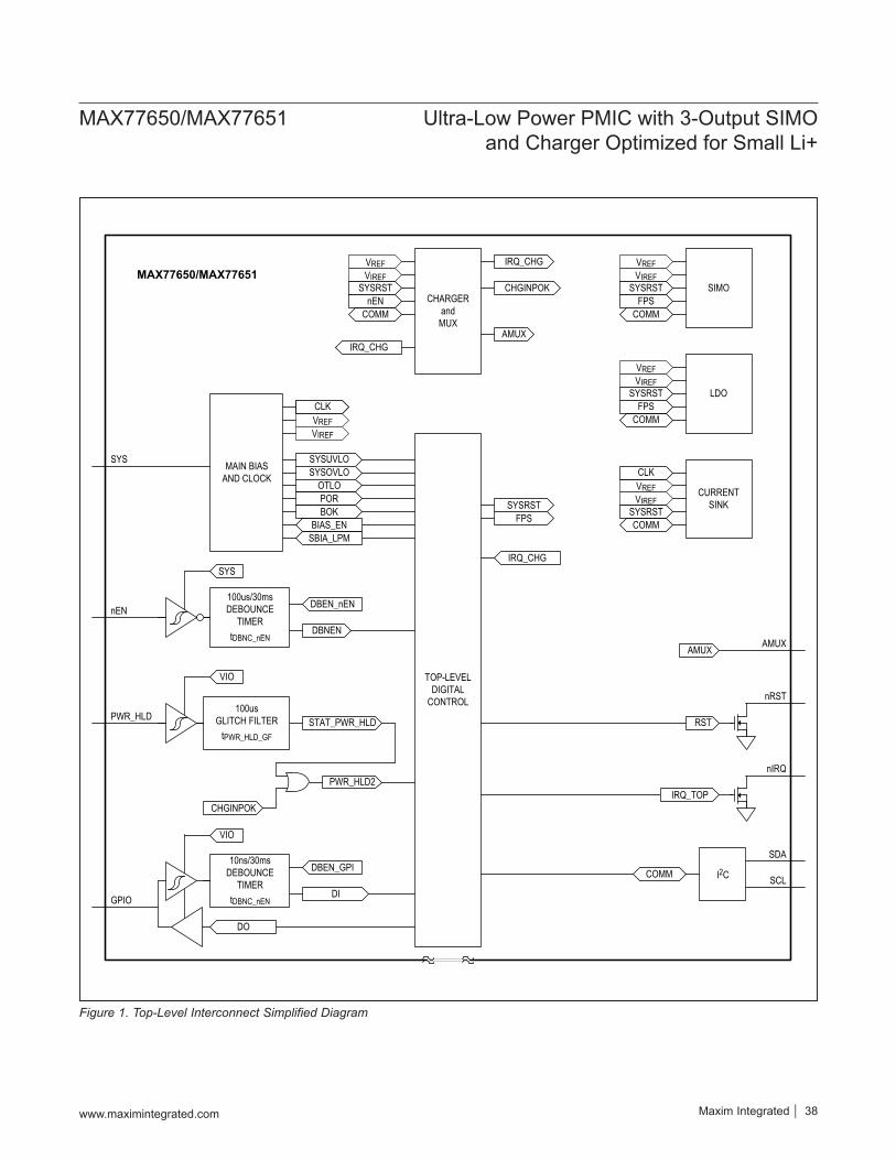
Figure 1. Top-Level Interconnect Simplified Diagram
nEN
SYS
nRST
RST
TOP-LEVEL DIGITAL
CONTROL
nIRQ
PWR_HLD
VIO
FPS
GPIO
VIO
MAIN BIAS AND CLOCK
SYS
SIMO
VREFVIREF
SYSRST
IRQ_TOP
SYSRST
CHGINPOK
SYSUVLOSYSOVLO
OTLOPORBOK
DO
COMMFPS
100usGLITCH FILTER
tPWR_HLD_GF
100us/30msDEBOUNCE
TIMERtDBNC_nEN
DI
AMUX
SDA
I2C SCL
BIAS_ENSBIA_LPM
PWR_HLD2
DBNEN
CLKVREFVIREF
CLK
AMUX
STAT_PWR_HLD
COMM10ns/30ms
DEBOUNCE TIMER
tDBNC_nEN
DBEN_GPI
DBEN_nEN
IRQ_CHG
LDO
VREFVIREF
SYSRSTFPS
COMM
CURRENT SINK
VREFVIREF
SYSRST
CLK
COMM
CHARGERandMUX
VREFVIREF
SYSRST CHGINPOK
IRQ_CHG
nENCOMM
IRQ_CHGAMUX
MAX77650/MAX77651
www.maximintegrated.com Maxim Integrated 38
MAX77650/MAX77651 Ultra-Low Power PMIC with 3-Output SIMO and Charger Optimized for Small Li+

Global ResourcesThe global resources encompass a set of circuits that serve the entire device and ensure safe, consistent, and reliable operation.
Features and Benefits Voltage Monitors
• SYS POR (power-on-reset) comparator generates a reset signal upon power-up
• SYS undervoltage ensures repeatable behavior when power is applied to and removed from the device
• SYS overvoltage monitor inhibits operation with overvoltage power sources to ensure reliability in faulty environments
Thermal Monitors• 165°C junction temperature shutdown
Manual Reset• 8s or 16s period
Wakeup Events• Charger insertion (with 120ms debounce)• nEN input assertion
Interrupt Handler• Interrupt output (nIRQ)• All interrupts are maskable
Pushbutton/Slide-Switch Onkey (nEN)• Configurable pushbutton/slide-switch functionality• 100μs or 30ms debounce timer interfaces directly
with mechanical switches On/Off Controller
• Startup/shut-down sequencing• Programable sequencing delay
PWR_HLD, GPIO, RST Digital I/Os
Voltage MonitorsThe device monitors the system voltage (VSYS) to ensure proper operation using three comparators (POR, UVLO, and OVLO). These comparators include hysteresis to prevent their outputs from toggling between states during noisy system transitions.
SYS POR ComparatorThe SYS POR comparator monitors VSYS and generates a power-on reset signal (POR). When VSYS is below VPOR, the device is held in reset (SYSRST = 1). When VSYS rises above VPOR, internal signals and on-chip memory stabilize and the device is released from reset (SYSRST = 0).
SYS Undervoltage Lockout ComparatorThe SYS undervoltage lockout (UVLO) comparator moni-tors VSYS and generates a SYSUVLO signal when the VSYS falls below UVLO threshold. The SYSUVLO signal is provided to the top-level digital controller. See Figure 4
and Table 2 for additional information regarding the UVLO comparator:
When the device is in the STANDBY state, the UVLO comparator is disabled.
When transitioning out of the STANDBY state, the UVLO comparator is enabled allowing the device to check for sufficient input voltage. If the device has sufficient input voltage, it can transition to the on state; if there is insufficient input voltage, the device transitions back to the STANDBY state.
SYS Overvoltage Lockout ComparatorThe device is rated for 5.5V maximum operating voltage (VSYS) with an absolute maximum input voltage of 6.0V. An overvoltage lockout monitor increases the robustness of the device by inhibiting operation when the supply volt-age is greater than VSYSOVLO. See Figure 4 and Table 2 for additional information regarding the OVLO comparator:
When the device is in the STANDBY state, the OVLO comparator is disabled.
nEN Enable InputnEN is an active-low internally debounced digital input that typically comes from the system’s on key. The debounce time is programmable with DBEN_nEN. The primary purpose of this input is to generate a wake-up signal for the PMIC that turns on the regulators. Maskable rising/falling interrupts are available for nEN (nEN_R and nEN_F) for alternate functionality.The nEN input can be configured to work either with a push-button (nEN_MODE = 0) or a slide-switch (nEN_MODE = 1). See Figure 2 for more information. In both pushbutton mode and slide-switch mode, the on/off con-troller looks for a falling edge on the nEN input to initiate a power-up sequence.
nEN Manual ResetnEN works as a manual reset input when the on/off con-troller is in the on via on/off controller state. The manual reset function is useful for forcing a power-down in case the communication with the processor fails. When nEN is configured for a push-button mode and the input is assert-ed (nEN = low) for an extended period (tMRST), the on/off controller initiates a power-down sequence and goes to standby mode. When nEN is configured for a slide-switch mode and the input is deasserted (nEN = high) for an extended period (tMRST), the on/off controller initiates a power-down sequence and goes to standby mode.A dedicated internal oscillator is used to create the 30ms (tDBNC_nEN) and 16s (tMRST) timers for nEN. Whenever the device is actively counting either of these times, the
www.maximintegrated.com Maxim Integrated 39
MAX77650/MAX77651 Ultra-Low Power PMIC with 3-Output SIMO and Charger Optimized for Small Li+

supply current increases by the oscillator's supply current (65μA when the battery voltage is at 3.7V). As soon as the event driving the timer goes away or is fulfilled, the oscillator automatically turns off and its supply current goes away.
nEN Dual-functionality: Push-Button vs. Slide-SwitchThe nEN digital input can be configured to work with a pushbutton switch or a slide-switch. The timing dia-gram below shows nEN's dual functionality for power-on sequencing and manual reset. The default configuration of the device is pushbutton mode (nEN_MODE = 0) and no additional programming is necessary. Applications that use a slide-switch on-key configuration must set nEN_MODE = 1 within tMRST.
Interrupts (nIRQ)Several status, interrupt, and interrupt mask registers monitor key information and assert the nIRQ output sig-nal when an interrupt event has occurred. Refer to the Programmer’s Guide for a comprehensive list of all inter-rupt bits and status registers.nIRQ is an active-low, open-drain output that is typically routed to the processor's interrupt input to allow for quick notification of interrupt events. A pullup resistor is required for this signal. This pullup resistor is typically found inside the processor that interprets the interrupt signal,
but a board-mounted pullup resistor is required if one is unavailable. The pullup resistor bias voltage should be less than or equal to VSYS.All interrupts are masked by default. Initialization software should unmask interrupts of interest so nIRQ can be asserted when they occur.
Reset Output (nRST)nRST is an open-drain, active-low output that is typically used to hold the processor in a reset state when the device is powered down. During a power-up sequence, the nRST deasserts after the last regulator in the power-up chain is enabled (tRSTODD). During a power-down sequence, the nRST output asserts before any regulator is powered down (tRSTOAD). See Figure 5 for nRST timing.A pullup resistor is required for the nRST open-drain out-put. This pullup resistor is typically inside the processor that is receiving the reset signal. A board-mounted pullup resistor is required if one is unavailable inside the proces-sor. The pullup resistor bias voltage should be less than or equal to VSYS.
Power Hold Input (PWR_HLD)PWR_HLD is an active-high digital input. PWR_HLD has a 100μs glitch filter (tPWR_HLD_GF). As shown in Figure 1, the output of this glitch filter is logically ORed with the wakeup signal coming from the charger to create a signal called PWR_HLD2 that drives the top-level digital control.
Figure 2. nEN Usage Timing Diagram
VSYS
STATE
NOT DRAWN TO SCALE
STANDBY POWER-ON SEQUENCE ON POWER-DOWN SEQUENCE
nEN
SYS
nEN
SYS
tDBNC_nEN
tDBNC_nEN
tDBNC_nEN
tMRST
tDBNC_nEN
tDBNC_nEN
tMRST
BATTERY INSERTION
PUSH-BUTTON MODE
SLIDE-SWITCH MODE
www.maximintegrated.com Maxim Integrated 40
MAX77650/MAX77651 Ultra-Low Power PMIC with 3-Output SIMO and Charger Optimized for Small Li+
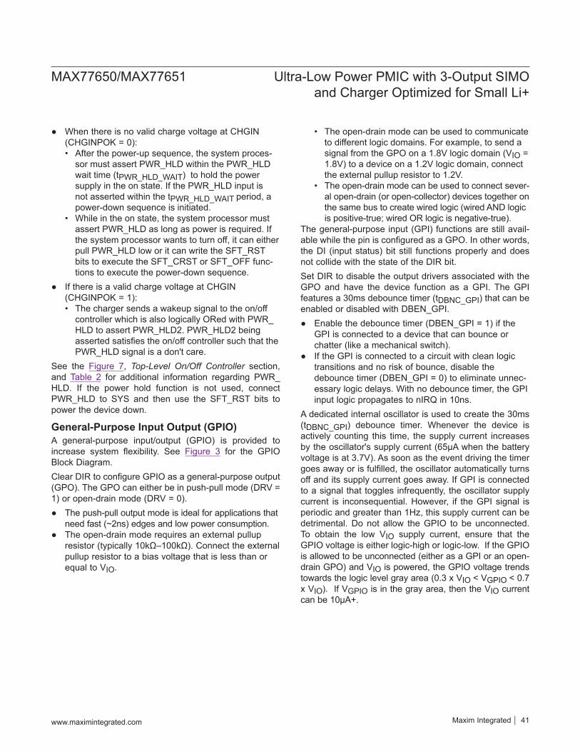
When there is no valid charge voltage at CHGIN (CHGINPOK = 0):• After the power-up sequence, the system proces-
sor must assert PWR_HLD within the PWR_HLD wait time (tPWR_HLD_WAIT) to hold the power supply in the on state. If the PWR_HLD input is not asserted within the tPWR_HLD_WAIT period, a power-down sequence is initiated.
• While in the on state, the system processor must assert PWR_HLD as long as power is required. If the system processor wants to turn off, it can either pull PWR_HLD low or it can write the SFT_RST bits to execute the SFT_CRST or SFT_OFF func-tions to execute the power-down sequence.
If there is a valid charge voltage at CHGIN (CHGINPOK = 1):• The charger sends a wakeup signal to the on/off
controller which is also logically ORed with PWR_HLD to assert PWR_HLD2. PWR_HLD2 being asserted satisfies the on/off controller such that the PWR_HLD signal is a don't care.
See the Figure 7, Top-Level On/Off Controller section, and Table 2 for additional information regarding PWR_HLD. If the power hold function is not used, connect PWR_HLD to SYS and then use the SFT_RST bits to power the device down.
General-Purpose Input Output (GPIO)A general-purpose input/output (GPIO) is provided to increase system flexibility. See Figure 3 for the GPIO Block Diagram.Clear DIR to configure GPIO as a general-purpose output (GPO). The GPO can either be in push-pull mode (DRV = 1) or open-drain mode (DRV = 0).
The push-pull output mode is ideal for applications that need fast (~2ns) edges and low power consumption.
The open-drain mode requires an external pullup resistor (typically 10kΩ–100kΩ). Connect the external pullup resistor to a bias voltage that is less than or equal to VIO.
• The open-drain mode can be used to communicate to different logic domains. For example, to send a signal from the GPO on a 1.8V logic domain (VIO = 1.8V) to a device on a 1.2V logic domain, connect the external pullup resistor to 1.2V.
• The open-drain mode can be used to connect sever-al open-drain (or open-collector) devices together on the same bus to create wired logic (wired AND logic is positive-true; wired OR logic is negative-true).
The general-purpose input (GPI) functions are still avail-able while the pin is configured as a GPO. In other words, the DI (input status) bit still functions properly and does not collide with the state of the DIR bit.Set DIR to disable the output drivers associated with the GPO and have the device function as a GPI. The GPI features a 30ms debounce timer (tDBNC_GPI) that can be enabled or disabled with DBEN_GPI.
Enable the debounce timer (DBEN_GPI = 1) if the GPI is connected to a device that can bounce or chatter (like a mechanical switch).
If the GPI is connected to a circuit with clean logic transitions and no risk of bounce, disable the debounce timer (DBEN_GPI = 0) to eliminate unnec-essary logic delays. With no debounce timer, the GPI input logic propagates to nIRQ in 10ns.
A dedicated internal oscillator is used to create the 30ms (tDBNC_GPI) debounce timer. Whenever the device is actively counting this time, the supply current increases by the oscillator's supply current (65μA when the battery voltage is at 3.7V). As soon as the event driving the timer goes away or is fulfilled, the oscillator automatically turns off and its supply current goes away. If GPI is connected to a signal that toggles infrequently, the oscillator supply current is inconsequential. However, if the GPI signal is periodic and greater than 1Hz, this supply current can be detrimental. Do not allow the GPIO to be unconnected. To obtain the low VIO supply current, ensure that the GPIO voltage is either logic-high or logic-low. If the GPIO is allowed to be unconnected (either as a GPI or an open-drain GPO) and VIO is powered, the GPIO voltage trends towards the logic level gray area (0.3 x VIO < VGPIO < 0.7 x VIO). If VGPIO is in the gray area, then the VIO current can be 10µA+.
www.maximintegrated.com Maxim Integrated 41
MAX77650/MAX77651 Ultra-Low Power PMIC with 3-Output SIMO and Charger Optimized for Small Li+

For example: If the GPI signal has a period of 60ms, the timer runs
continuously, and the supply current increases by the full 65μA.
If the signal has a longer period, the supply current increase by a fraction of 65μA; a period of 120ms increases the supply current by 50% of the 65μA oscillator current (60ms/120ms x 65μA = 32.5μA).
The GPI features edge detectors that feed into the top-level interrupt system of the chip. This allows software to use interrupts to service events associ-ated with a GPI change instead of having to poll for these changes.
If the application wants nIRQ to go low only on a GPI rising edge, then it should clear the GPI rising edge interrupt mask bit (GPI_RM = 0) and set the GPI fall-ing edge interrupt mask bit (GPI_FM = 1).
If the applications wants nIRQ to go low only on a GPI falling edge, then it should set the GPI rising edge interrupt mask bit (GPI_RM = 1) and clear the GPI falling edge interrupt mask bit (GPI_FM = 0).
If the applications wants nIRQ to go low on both GPI falling and rising edges, then it should clear the GPI rising edge interrupt mask bit (GPI_RM = 0) and clear the GPI falling edge interrupt mask bit (GPI_FM = 0).
Figure 3. GPIO Block Diagram
LOGIC
COMM
GPIO
VIO
D
R
Q 1
READ
D
R
Q 1
READ(GPI_R)
(GPI_F)
GPI_RGPI_RM
GPI_FMGPI_F
nIRQ
IRQ
CNFG_GPIO
SYSDRV
DIR
DO
DIGPI_RGPI_F
GPI_RMGPI_FM
DRV
DIR
DO
GND
DBNC_EN
30ms DEBOUNCE (tDBNC_GPI)
01
DI
DBNC_EN
OTHER nIRQ ASSERTION SOURCES NOT SHOWN
www.maximintegrated.com Maxim Integrated 42
MAX77650/MAX77651 Ultra-Low Power PMIC with 3-Output SIMO and Charger Optimized for Small Li+

On/Off ControllerThe on/off controller monitors multiple power-up (wakeup) and power-down (shutdown) conditions to enable or dis-able resources that are necessary for the system and its processor to move between its operating modes.Many systems have one power management controller and one processor and rely on the on/off controller to be the master controller. In this case, the on/off controller receives the wakeup events and enables some or all of the regulators in order to power up a processor. That pro-cessor then manages the system. To conceptualize this master operation see Figure 4 and Table 2. A typical path through the on/off controller in master mode is:
Start in the no power state. Apply a battery to the system and transition through
path 1 and 2 to the standby state. Press the system's on key (nEN = low) and transition
through path 3A and 4 to the "PWR_HLD?" state. The processor boots up and drives PWR_HLD high,
which drives the transition through path 4C to the on through the on/off controller state.
The device performs its desired functions in the on through on/off controller state. When it is ready to turn off, the processor drives PWR_HLD low that drives the transition through path 5B and 8 to the standby state.
Some systems have several power management blocks, a main processor, and subprocessors. These systems can use this device as a subpower management block for a peripheral portion of circuitry as long as there is an I2C port available from a higher level processor. To concep-tualize this slave operation, see Figure 4 and Table 2. A typical path through the on/off controller in slave mode is:
Start in the no power state. Apply a battery to the system and transition through
path 1 and 2 to the standby state. When the higher level processor wants to turn on this
device's resources, it enables the main bias circuits through I2C (SBIA_EN = 1) to transition along path 2A to the on through software state.
The higher level processor can now control this device's resources with I2C commands (i.e., turn on/off regulators).
When the higher level processor is ready to turn this device off, it turns off everything through I2C and then disables the main bias circuits through I2C (SBIA_EN = 0) to transition along path 2B to the standby state.
Note that in this slave style of operation, the SFT_RST bits should not be used to turn the device off. The SFT_RST bits establish directives to the on/off controller itself that does not make sense in slave mode. In slave mode, since the I2C commands enable the device's resources, they should also disable them.
www.maximintegrated.com Maxim Integrated 43
MAX77650/MAX77651 Ultra-Low Power PMIC with 3-Output SIMO and Charger Optimized for Small Li+

Figure 4. Top-Level On/Off Controller
X
TRANSITION NAME. SEE TABLE 2
STATE
ACTION
DECISION
3A
POWER UP SEQUENCE(FIGURE 5)
4B
STANDBY
3
DISABLE MAIN BIAS
POWER DOWN SEQUENCE(FIGURE 5)
4
4C
4A
ENABLE MAIN BIAS
6
IMMEDIATE SHUTDOWN(FIGURE 5)
9
ENABLE MAIN BIAS
86
NO POWERVCGHIN=0, VSYS<VPOR
0
POWER-ON RESET (POR)
1
2
2A
5A
7
3
3
ON VIA SOFTWARE
2B
ON VIA ON/OFF CONTROLLER 5B
PWR_HLD?
11
12
2B
10
10
ANY STATE
ANY STATE
www.maximintegrated.com Maxim Integrated 44
MAX77650/MAX77651 Ultra-Low Power PMIC with 3-Output SIMO and Charger Optimized for Small Li+

TRANSITION/STATE CONDITION0 System voltage is below the POR threshold (VSYS < VPOR).1 System voltage is above the POR threshold (VSYS > VPOR).2 Internal signals and on-chip memory stabilize and the device is released from reset.
STANDBY
The device is waiting for a wake-up signal or an I2C command to enable the main bias circuits.* This is the lowest current state of the device (IQ ~0.3μA).* Main bias circuits are off, POR comparator is on.* I2C is on when VIO is valid.* Peripheral functions (LDO, SIMO, LEDs, AMUX) do not operate in this state because the main bias circuits are off. To utilize a function enter the on through software or on through on/off controller states.
2A Main bias circuits enabled through I2C (SBIA_EN = 1).2B Main bias circuits disabled through I2C (SBIA_EN = 0).
ON VIA SOFTWARE*
The main bias circuits are enabled through software and all peripheral functions (LDO, SIMO, LEDs, AMUX) can be manually enabled or disabled through I2C.
3
A wake-up signal has been received.* A debounced onkey (nEN) falling edge has been detected (DBNEN = 1) or* A charge source has been applied and a rising edge on CHGIN has been detected and debounced (tCHGIN-DB ~120ms) or* Internal wake-up flag has been set due to SFT_RST = 0b01 (WKUP = 1)
3A Main bias circuits are OK (BOK = 1)4 Power-up sequence complete.
4A PWR_HLD wait time has expired and PWR_HLD2 is low (t > tPWR_HLD_WAIT && PWR_HLD2 = 0).4B PWR_HLD wait time has not expired and PWR_HLD2 is low (t < tPWR_HLD_WAIT && PWR_HLD2 = 0).4C PWR_HLD2 = 1
ON VIA ON/OFF CONTROLLER*
On state.* All flexible power sequencers (FPS) are on.* The main bias circuits are enabled.* IQ ~5.6µA (typ) with all regulators enabled (no load) and the main bias circuits in low power mode.
5A PWR_HLD2 = 1
5B
PWR_HLD2 = 0 ORSystem overtemperature lockout (TJ >TOTLO) orSoftware cold reset (SFT_RST[1:0] = 0b01) orSoftware power off (SFT_RST[1:0] = 0b10) orManual reset occurred. See the nEN Manual Reset section for more information.
6System overtemperature lockout (TJ >TOTLO) orSystem undervoltage lockout (VSYS < VSYSUVLO + VSYSUVLO_HYS) orSystem overvoltage lockout (VSYS > VSYSOVLO)
7System undervoltage lockout (VSYS < VSYSUVLO) orSystem overvoltage lockout (VSYS > VSYSOVLO)Note: The overvoltage lockout transition does not apply to the ON VIA SOFTWARE state.
8 Finished with the power-down sequence.9 Finished with immediate shutdown.
10 System overtemperature lockout (TJ > TOTLO).11 Done disabling main bias.12 Done enabling main bias.
Table 2. On/Off Controller Transition/State
www.maximintegrated.com Maxim Integrated 45
MAX77650/MAX77651 Ultra-Low Power PMIC with 3-Output SIMO and Charger Optimized for Small Li+

Figure 5. Power-Up/Power-Down Sequence
FPS ENABLE SLOT 2
STARTFROM TOP LEVEL #3A
ENDTO TOP LEVEL #4
WAIT tEN
WAIT tEN
WAIT tRSTODD
DE-ASSERT nRST
FPS DISABLE SLOT 2
WAIT tDIS
WAIT tDIS
WAIT tRSTOAD
ASSERT nRST
SET THE APPROPRIATE BIT IN THE EVENT RECORDER REGISTER (ERCFLAG) TO INDICATE
THE SOURCE OF THE POWER DOWN EVENT.
START FROM TOP LEVEL #4A OR #5B
SFT_RST = 0b01
SFT_RST = 0b10 OR PWR_HLD2 = 0
SET WAKEUP FLAG (WKUP = 1)
CLEAR WAKEUP FLAGS
WAIT 60ms
FPS ENABLE SLOT 3
WAIT tEN
WAIT tDIS
TEMPERATURE IS OKAY(TJ<TOTLO)
OTLO?
CLEAR WAKEUP FLAG (WKUP = 0) TEMPERATURE IS
NOT OKAY (TJ>TOTLO)
IMMEDIATE SHUTDOWN
FPS ENABLE SLOT 1
FPS ENABLE SLOT 0
FPS DISABLE SLOT 3
FPS DISABLE SLOT 1
FPS DISABLE SLOT 0DISABLE FPS3, FPS2, FPS1, FPS0
ASSERT nRST
ENDTO TOP LEVEL #9
SET THE APPROPRIATE BIT IN THE EVENT RECORDER REGISTER (ERCFLAG) TO INDICATE
THE SOURCE OF THE POWER DOWN EVENT.
STARTFROM TOP LEVEL #7
WAIT 125ms
RESET DEVICE (PULSE SYSRST FOR 5µs)
ENDTO TOP LEVEL #8
WAIT 125ms
RESET DEVICE (PULSE SYSRST FOR 5µs)
SFT_RST = 0b00 OR PWR_HLD2 = 1
RETURN BACK TO THE ON STATE
POWER-UP SEQUENCE POWER-DOWN SEQUENCE
www.maximintegrated.com Maxim Integrated 46
MAX77650/MAX77651 Ultra-Low Power PMIC with 3-Output SIMO and Charger Optimized for Small Li+

Flexible Power SequencerThe flexible power sequencer (FPS) allows resources to power up under hardware or software control. Additionally, each resource can power up independently or among a group of other regulators with adjustable power-up and pow-er-down delays (sequencing). Figure 6 shows four resources powering up under the control of flexible power sequencer.
The flexible sequencing structure consists of 1 master sequencing timer and 4 slave resources (SBB0, SBB1, SBB2, and LDO). When the FPS is enabled, a master timer generates four sequencing events for device power-up and power-down.
Figure 6. Flexible Power Sequencer Basic Timing Diagram
FPS RESOURCES
PLSFPS
tEN SAME FOR ALL FPS ENABLE PULSES
0 1 2 3
LDO
SBB1
SBB2
ENFPS
tDIS SAME FOR ALL FPS DISABLE PULSES tDIS = 2x tEN
0123
SBB0
NOT DRAWN TO SCALE
www.maximintegrated.com Maxim Integrated 47
MAX77650/MAX77651 Ultra-Low Power PMIC with 3-Output SIMO and Charger Optimized for Small Li+

Figure 7. Startup Timing Diagram Due to nEN
VSYS
BATTERY INSERTION
tPOR~100µs
PORNO POWER STANDBY
nEN
tDBNC_nEN
POWER-UP SEQUENCE
REGULATORS
nRST
PWR_HLD
tPWR_HLD_WAIT
ON THROUGH ON/OFF CONTROLLERPWR_HLD?
tEN tEN
NOTES: 1 – nEN LOGIC INPUT IS CONFIGURED TO PUSHBUTTON MODE AND HAS AN EXTERNAL PULLUP TO SYS.2 – nEN ASSERTION RESULTS IN A WAKE-UP EVEN AFTER A DEBOUNCE TIME (tDBNCEN).3 – INTERNAL WAKE-UP SIGNAL CAN ALSO BE GENERATED BY CHARGER PLUG-IN EVENT.
4 – nIRQ HAS AN EXTERNAL PULLUP TO VIO WHICH IS ENABLED IN FLEXIBLE POWER SEQUENCER SLOT #15 – SYSTEM PROCESSOR ASSERTS PWR_HLD INPUT TO PLACE THE DEVICE IN THE ON THROUGH ON/OFF CONTROLLER STATE.6 – AS PART OF ITS INITIALIZATION ROUTINE, SOFTWARE READS THE INTERRUPT REGISTERS (CLEAR ON READ) AND PROGRAMS THE INTERRUPT MASKS AS DESIRED.
NOT DRAWN TO SCALE
VPOR~1.9V
NOTE 5
NOTE 2
STATE
BIAS EN(INTERNAL)
tDBNC_nEN
nIRQ
SYSTEM SOFTWARE
STAT_EN
tRSTODD
FPS0 FPS1 FPS2tEN
FPS3
INTERNAL WAKE-UP SIGNAL NOTE 3
NOTE 1
NOTE 4
nEN_F
nEN_R
NOTE 6
tSBIA_EN
www.maximintegrated.com Maxim Integrated 48
MAX77650/MAX77651 Ultra-Low Power PMIC with 3-Output SIMO and Charger Optimized for Small Li+

Figure 8. Startup Timing Diagram Due to Charge Source Insertion
VSYS
CHARGER INSERTION
CHGIN DEBOUNCESTATE
nEN
POWER-UP SEQUENCE
REGULATORS
nRST
PWR_HLD2
tPWR_HLD_WAIT
ON THROUGH ON/OFF CONTROLLERPWR_HLD?
tEN tEN tEN
tRSTODD
VCHGIN
CHGINOK=1
VBATT
tCHGIN-DB (~120ms)
CHG_EN = 1CHARGER ENABLED
SYST
EM V
OLTA
GEBA
TTER
Y VO
LTAG
E
PRE-QUAL FAST CHARGE (CC) TOP-OFF (CV) DONE
IPQ
VFAST-CHG
ITOPOFF
VPQ
VFAST-CHG
CHAR
GER
VOLT
AGE
CHAR
GE C
URRE
NT
0V
0V
0V
0mA
5V
INTERNAL CHARGER GENERATED WAKE SIGNAL NOTE 3
VPOR~2.0VVSYSUVLO~2.9V
NOTE 5
NOTE 2
NOTE 1
NOTES: 1 – nEN LOGIC INPUT IN CONFIGURED TO PUSHBUTTON MODE AND HAS AN EXTERNAL PULLUP TO SYS.
2 – IF PWR_HLD IS NOT ASSERTED BY THE END OF THE tPWR_HLD_WAIT PERIOD, DEVICE INITIATES A POWER-DOWN SEQUENCE.3 - IF CHG_EN = 1 (@ OTP) THEN THE CHARGER ENABLED EVENT COINCIDES WITH THE WAKE EVENT (CHARGING START ALONG WITH POWER-UP SEQUENCE).4 – THIS INFLECTION POINT IS SYMBOLIC OF BATTERY PROTECTION FET CLOSING5 – SOFTWARE SETS CHG_EN = 1 TO ENABLE CHARGING. IF CHG_EN = 1 AT OTP, SEE NOTE 3.
- - - - BLUE DOTTED LINES ARE USER INITIATED EVENTS
NOTE 4
IBATT
VSYS-REG
VFAST-CHG
FPS0 FPS1 FPS2 FPS3
tSBIA_EN
www.maximintegrated.com Maxim Integrated 49
MAX77650/MAX77651 Ultra-Low Power PMIC with 3-Output SIMO and Charger Optimized for Small Li+

Debounced Inputs (nEN, GPI, CHGIN)nEN, CHGIN, and GPIO (when operating as an input), are debounced on both rising and falling edges to reject unde-sired transitions. The input must be at a stable logic level
for the entire debounce period for the output to change its logic state. Figure 9 shows an example timing diagram for the nEN debounce.
Figure 9. Debounced Inputs
nEN
DBEN
EN
tDBUF
tDBNCEN
BOUNCING IS REJECTED
tDBUF
tDBNCEN
BOUNCING IS REJECTED
STABLE SIGNALS IS ACCEPTED
STABLE SIGNAL IS ACCEPTED
(INTERNAL)
(INTERNAL)
www.maximintegrated.com Maxim Integrated 50
MAX77650/MAX77651 Ultra-Low Power PMIC with 3-Output SIMO and Charger Optimized for Small Li+

Smart Power Selector ChargerThe linear Li+ charger features Maxim's smart power selector. This allows separate input current limit and bat-tery charge current settings. Batteries charge faster under the supervision of the smart power selector because charge current is independently regulated and not shared with variable system loads. See the Smart Power Selector section for more information.The programmable constant-current charge rate (7.5mA to 300mA) supports a wide range of battery capacities. The programmable input current limit (0mA to 475mA) supports a range of charge sources, including USB. The charger's programmable battery regulation voltage range (3.6V–4.6V) supports a wide variety of cell chemistries. Small battery capacities are supported; the charger accu-rately terminates charging by detecting battery currents as low as 0.375mA.
Additionally, the robust charger input withstands overvoltag-es up to 28V. To enhance charger safety, an NTC thermis-tor provides temperature monitoring in accordance with the JEITA recommendations. See the Adjustable Thermistor Temperature Monitors section for more information.
Features 7.25V maximum operating input voltage with 28V
input standoff 7.5mA to 300mA programmable fast-charge current Programmable termination current from 0.375mA to
45mA Programmable battery regulation voltage from 3.6V
to 4.6V < 1μA battery-only supply current Instant-on functionality Analog multiplexer enables power monitoring JEITA battery temperature monitor adjusts current
and battery regulation voltage for safe charging Programmable die temperature regulation
Figure 10. Linear Charger Simplified Block Diagram
www.maximintegrated.com Maxim Integrated 51
MAX77650/MAX77651 Ultra-Low Power PMIC with 3-Output SIMO and Charger Optimized for Small Li+

Charger Symbol Reference GuideTable 3 lists the names and functions of charger-specific signals and if they can be programmed through I2C. Consult the Electrical Characteristics and Programmer’s Guide for more information.
Figure 11 indicates the high-level functions of each control circuit within the linear charger.
SYMBOL NAME I2C PROGRAMMABLE?VCHGIN_OVP CHGIN overvoltage threshold NoVCHGIN_UVLO CHGIN undervoltage lockout threshold NoVCHGIN-MIN Minimum CHGIN voltage regulation setpoint Yes, through VCHGIN_MIN[2:0]ICHGIN-LIM CHGIN input current limit Yes, through ICHGIN_LIM[2:0]VSYS-REG SYS voltage regulation target Yes, through VSYS_REG[4:0]VSYS-MIN Minimum SYS voltage regulation setpoint No, tracks VSYS-REGVFAST-CHG Fast-charge constant-voltage level Yes, through CHG_CV[5:0]IFAST-CHG Fast-charge constant-current level Yes, through CHG_CC[5:0]IPQ Prequalification current level Yes, through I_PQVPQ Prequalification voltage threshold Yes, through CHG_PQ[2:0]ITERM Termination current level Yes, through I_TERM[1:0]TJ-REG Die temperature regulation setpoint Yes, through TJ_REG[2:0]tPQ Prequalification safety timer NotFC Fast-charge safety timer Yes, through T_FAST_CHG[1:0]tTO Top-off timer Yes, through T_TOPOFF[2:0]
Table 3. Charger Quick Symbol Reference Guide
Figure 11. Charger Simplified Control Loops
BODY-SWITCH
VCHGIN-MINVCHGIN_OVP
VCHGIN_UVLO
ICHGIN-LIM
TJ-REG
VSYS-REG
DIE TEMP MONITOR
CHARGE CONTROLLER
VSYS-MIN
IFAST-CHG
IPQ ITERM
VFAST-CHGVPQ
SYS
BATT
CHGIN
INPUT CONTROLLER
tPQtFCtTO
TIMER
BODY-SW
ITCH
www.maximintegrated.com Maxim Integrated 52
MAX77650/MAX77651 Ultra-Low Power PMIC with 3-Output SIMO and Charger Optimized for Small Li+

Smart Power SelectorThe smart power selector seamlessly distributes power from the input (CHGIN) to the battery (BATT) and the sys-tem (SYS). The smart power selector basic functions are:
When the system load current is less than the input current limit, the battery is charged with residual power from the input.
When a valid input source is connected, the sys-tem regulates to VSYS-REG to power system loads regardless of the battery's voltage (instant on).
When the system load current exceeds the input cur-rent limit, the battery provides additional current to the system (supplement mode).
When the battery is finished charging and an input source is present to power the system, the battery remains disconnected from the system.
When the battery is connected and there is no input power, the system is powered from the battery.
Input Current LimiterThe input current limiter limits CHGIN current so as not to exceed ICHGIN-LIM (programmed by ICHGIN_LIM[2:0]). A maskable interrupt (CHGIN_CTRL_I) is available to signal when the input current limit engages. The state of this loop is reflected by the ICHGIN_LIM_STAT bit.The input circuit is capable of standing off 28V from ground. CHGIN suspends power delivery to the sys-tem and battery when VCHGIN exceeds VCHGIN_OVP (7.5V typical). The input circuit also suspends when VCHGIN falls below VCHGIN_UVLO minus 500mV of hys-teresis (3.5V typical). While in OVP or UVLO, the charger remains off, and the battery provides power to the system.When an valid charge source is connected to CHGIN, SYS begins delivering power to the system after a 120ms debounce timer (tCHGIN-DB).A maskable interrupt (CHGIN_I) signals changes in the state of CHGIN's voltage quality. The state of CHGIN is reflected by CHGIN_DTLS[1:0].
Minimum Input Voltage RegulationIn the event of a poor-quality charge source, the mini-mum input voltage regulation loop works to reduce input current if VCHGIN falls below VCHGIN-MIN (programmed by VCHGIN_MIN[2:0]). This is important because many commonly used charge adapters feature foldback protec-tion mechanisms where the adapter completely shuts off if its output droops too low. The minimum input voltage
regulation loop also prevents VCHGIN from dropping below VCHGIN_UVLO if the cable between the charge source and the charger's input is long or highly resistive.The input voltage regulation loop improves performance with current limited adapters. If the charger’s input current limit is programmed above the current limit of the given adapter, the input voltage loop allows the input to regulate at the current limit of the adapter. The input voltage regu-lation loop also allows the charger to perform well with adapters that have poor transient load response times.A maskable interrupt (CHGIN_CTRL_I) signals when the minimum input voltage regulation loop engages. The state of this loop is reflected by VCHGIN_MIN_STAT.
Minimum System Voltage RegulationThe minimum system voltage regulation loop ensures that the system rail remains close to the programmed SYS regulation voltage (VSYS-REG) regardless of system load-ing. The loop engages when the combined battery charge current and system load current causes the CHGIN input to current-limit at ICHGIN-LIM. When this happens, the minimum system voltage loop reduces charge current in an attempt to keep the input out of current limit, thereby keeping the system voltage above VSYS-MIN (VSYS-REG - 100mV typical). If this loop reduces battery current to 0 and the system is in need of more current than the input can provide, then the smart power selector overrides the minimum system voltage regulation loop and allows SYS to collapse to BATT for the battery to provide supplement current to the system. The smart power selector automati-cally reenables the minimum system voltage loop when the supplement event has ended.A maskable interrupt (SYS_CTRL_I) asserts to signal a change in VSYS_MIN_STAT. This status bit asserts when the minimum system voltage regulation loop is active.
Die Temperature RegulationIn case the die temperature exceeds TJ-REG (pro-grammed by TJ_REG[2:0]) the charger attempts to limit the temperature increase by reducing battery charge current. The TJ_REG_STAT bit asserts whenever charge current is reduced due to this loop. The charger's cur-rent sourcing capability to SYS remains unaffected when TJ_REG_STAT is high. A maskable interrupt (TJ_REG_I) asserts to signal a change in TJ_REG_STAT. It is advis-able that the TJ_REG_I interrupt be used to signal the system processor to reduce loads on SYS to reduce total system temperature.
www.maximintegrated.com Maxim Integrated 53
MAX77650/MAX77651 Ultra-Low Power PMIC with 3-Output SIMO and Charger Optimized for Small Li+

Charger State MachineThe battery charger follows a strict state-to-state progres-sion to ensure that a battery is charged safely. The status
bitfield, CHG_DTLS[3:0], reflects the charger's current operational state. A maskable interrupt (CHG_I) is avail-able to signal a change in CHG_DTLS[3:0].
Figure 12. Charger State Diagram
DONECHG_DTLS[3:0] = 0b1000
CHG = 0
FAST-CHARGE (CC)CHG_DTLS[3:0] = 0b0010
CHG = 1IBATT = IFAST-CHG**
ANY STATE
CHGIN INSERTED (CHGIN_DTLS[1:0] = 0b10)
TIME ELAPSED > tPQPREQUALIFICATION
CHG_DTLS[3:0] = 0b0001CHG = 1
IBATT = IPQ
VBATT > VPQ
TOP-OFFCHG_DTLS[3:0] = 0b0110
CHG = 1VBATT = VFAST-CHG
VBATT < VPQ – 100mV
CHARGER OFFCHG_DTLS[3:0] = 0b0000
CHG = 0
PREQUALIFICATIONTIMER FAULT
CHG_DTLS[3:0] = 0b1010CHG = 0
FAST-CHARGETIMER FAULT
CHG_DTLS[3:0] = 0b1011CHG = 0
FAST-CHARGE (CV)CHG_DTLS[3:0] = 0b0100
CHG = 1VBATT = VFAST-CHG
VBATT = VFAST-CHGVBATT < VFAST-CHG
IBATT < ITERM
TIME ELAPSED > tTO
VBATT < VFAST-CHG – 150mVCHGIN INVALID
(CHGIN_DTLS[1:0] = 0b00 or 0b01)OR
CHARGER DISABLED(CHG_EN = 0)
BATTERY TEMPERATUREFAULT
CHG_DTLS[3:0] = 0b1100CHG = 0
TIMERS PAUSE IN THIS STATE,RESUME ON EXIT.
JEITA-MODIFIEDFAST-CHARGE (CV)
CHG_DTLS[3:0] = 0b0101CHG = 1
VBATT = VFAST-CHG_JEITA
THM_EN = 1AND
CHG_EN = 1AND
(TBATT > THOT OR TBATT < TCOLD)
VBATT = VFAST-CHG_JEITAVBATT <
VFAST-CHG_JEITA
JEITA-MODIFIED TOP-OFF
CHG_DTLS[3:0] = 0b0111CHG = 1
VBATT = VFAST-CHG_JEITA
RETURNS TO SAME STATE WHEN: THM_EN = 0OR(TBATT < THOT AND TBATT > TCOLD)
JEITA-MODIFIEDFAST-CHARGE (CC)
CHG_DTLS[3:0] = 0b0011CHG = 1
IBATT = IFAST-CHG_JEITA**
V BAT
T < V
FAST
-CHG
_JEI
TA –
150m
V
DE-BOUNCECHG_DTLS[3:0] = 0b0000
CHG = 0
TIME ELAPSED < tCHGIN-DB
CHGIN DE-BOUNCEDTIME ELAPSED >= tCHGIN-DB(CHGIN_DTLS[1:0] = 0b11)
VBATT < VPQ – 100mV
*TIME ELAPSED IS AGGREGATED THROUGHOUT THE FAST-CHARGE AND JEITA-MODIFIED FAST-CHARGE STATES. ALL FAST-CHARGE STATES (REGARDLESS OF JEITA STATUS) SHARE THE SAME SAFETY TIMER.
**IFAST-CHG MAY BE REDUCED BY THE MINIMUM INPUT VOLTAGE REGULATION LOOP, THE MINIMUM SYSTEM VOLTAGE REGULATION LOOP, OR THE DIE TEMPERATURE REGULATION LOOP.
IBATT > ITERMIBATT < ITERMIBATT > ITERM
CHARGER ENABLED (CHG_EN = 1) ANDCHGIN DE-BOUNCED & VALID (CHGIN_DTLS[1:0] = 0b11) ANDBATTERY LOW BY VRESTART (VBATT < VFAST-CHG – 150mV)
TIME ELAPSED* > tFC
THM_EN = 1 AND(TBATT > TWARM OR TBATT < TCOOL)
THM_EN = 0 OR(TBATT < TWARM AND TBATT > TCOOL)
THM_EN = 1 AND(TBATT > TWARM OR TBATT < TCOOL)
THM_EN = 0 OR(TBATT < TWARM AND TBATT > TCOOL)
THM_EN = 1 AND(TBATT > TWARM OR TBATT < TCOOL)
THM_EN = 0 OR(TBATT < TWARM AND TBATT > TCOOL)
THM_EN = 0 OR(TBATT < TWARM AND TBATT > TCOOL)
JEITA-MODIFIED DONECHG_DTLS[3:0] = 0b1001
CHG = 0
TIME ELAPSED > tTO
ANY FAST-CHARGE ORJEITA-MODIFIED FAST-CHARGE
STATECHG_DTLS[3:0] = 0b0010-0b0101
CHG = 1
www.maximintegrated.com Maxim Integrated 54
MAX77650/MAX77651 Ultra-Low Power PMIC with 3-Output SIMO and Charger Optimized for Small Li+

Charger Off StateThe charger is off when CHGIN is invalid, the charger is disabled, or the battery is fresh.CHGIN is invalid when the CHGIN input is invalid (VCHGIN < VCHGIN_UVLO or VCHGIN > VCHGIN_OVP). While CHGIN is invalid, the battery is connected to the system. CHGIN voltage quality can be separately moni-tored by the CHGIN_DTLS[1:0] status bitfield. Refer to the Programmer’s Guide for details.The charger is disabled when the charger enable bit is 0 (CHG_EN = 0). The battery is connected or disconnected to the system depending on the validity of VCHGIN while CHG_EN = 0. See the Smart Power Selector section.The battery is fresh when CHGIN is valid and the charger is enabled (CHG_EN = 1) and the battery is not low by VRESTART (VBATT > VFAST-CHG - VRESTART). The bat-tery is disconnected from the system and not charged while the battery is fresh. The charger state machine exits this state and begin charging when the battery becomes low by VRESTART (150mV typical). This condition is func-tionally similar to done state. See Done State section.
Prequalification StateThe prequalification state is intended to assess a low-volt-age battery's health by charging at a reduced rate. If the battery voltage is less than the VPQ threshold, the charger is automatically in prequalification. If the cell voltage does not exceed VPQ in 30 minutes (tPQ), the charger faults. The prequalification charge rate is a percentage of IFAST-CHG and is programmable with I_PQ. The prequalifica-tion voltage threshold (VPQ) is programmable through CHG_PQ[2:0].
Fast-Charge StatesWhen the battery voltage is above VPQ, the charger transitions to the fast-charge (CC) state. In this state, the charger delivers a constant current (IFAST-CHG) to the cell. The constant current level is programmable from 7.5mA to 300mA by CHG_CC[5:0].When the cell voltage reaches VFAST-CHG, the charger state machine transitions to fast-charge (CV). VFAST-CHG is programmable with CHG_CV[5:0] from 3.6V to 4.6V. The charger holds the battery's voltage constant at VFAST-CHG while in the fast-charge (CV) state. As the battery approaches full, the current accepted by the battery reduces. When the charger detects that battery charge current has fallen below ITERM, the charger state machine enters the top-off state.
A fast-charge safety timer starts when the state machine enters fast-charge (CC) or JEITA-modified fast-charge (CC) from a non-fast-charge state. The timer continues to run through all fast-charge states regardless of JEITA sta-tus. The timer length (tFC) is programmable from 3 hours to 7 hours in 2 hour increments with T_FAST_CHG[1:0]. If it is desired to charge without a safety timer, program T_FAST_CHG[1:0] with 0b00 to disable the feature. If the timer expires before the fast-charge states are exited, the charger faults. See the Fast-Charge Timer Fault State section for more information.If the charge current falls below 20% of the programmed value during fast-charge (CC), the safety timer pauses. The timer also pauses for the duration of supplement mode events. The TIME_SUS bit indicates the status of the fast-charge safety timer. Refer to the Programmer’s Guide for more details.
Top-Off StateTop-off state is entered when the battery charge cur-rent falls below ITERM during the fast-charge (CV) state. ITERM is a percentage of IFAST-CHG and is program-mable through I_TERM[1:0]. While in the top-off state, the battery charger continues to hold the battery's voltage at VFAST-CHG. A programmable top-off timer starts when the charger state machine enters the top-off state. When the timer expires, the charger enters the done state. The top-off timer value (tTO) is programmable from 0 minutes to 35 minutes with T_TOPOFF[2:0]. If it is desired to stop charging as soon as battery current falls below ITERM, program tTO to 0 minutes.
Done StateThe charger enters the done state when the top-off timer expires. The battery remains disconnected from the system during done. The charger restarts if the battery voltage falls more than VRESTART (150mV typ) below the programmed VFAST-CHG value.
Prequalification Timer Fault StateThe prequalification timer fault state is entered when the battery's voltage fails to rise above VPQ in tTO (30 min-utes typical) from when the prequalification state was first entered. If a battery is too deeply discharged, damaged, or internally shorted, the prequalification timer fault state can occur. During the timer fault state, the charger stops delivering current to the battery and the battery remains disconnected from the system. To exit the prequalification timer fault state, toggle the charger enable (CHG_EN) bit or unplug and replug the external voltage source con-nected to CHGIN.
www.maximintegrated.com Maxim Integrated 55
MAX77650/MAX77651 Ultra-Low Power PMIC with 3-Output SIMO and Charger Optimized for Small Li+

Fast-Charge Timer Fault StateThe charger enters the fast-charge timer fault state if the fast-charge safety timer expires. While in this state, the charger stops delivering current to the battery and the battery remains disconnected from the system. To exit the fast-charge timer fault state, toggle the charger enable bit (CHG_EN) or unplug and replug the external voltage source connected to CHGIN.
Battery Temperature Fault StateIf the thermistor monitoring circuit reports that the battery is either too hot or too cold to charge (as programmed by THM_HOT[1:0] and THM_COLD[1:0]), the state machine enters the battery temperature fault state. While in this state, the charger stops delivering current to the battery and the battery remains disconnected from the system. This state can only be entered if the thermistor is enabled (THM_EN = 1). Battery temperature fault state has prior-ity over any other fault state, and can be exited when the thermistor is disabled (THM_EN = 0) or when the battery returns to an acceptable temperature. When this fault state is exited, the state machine returns to the last state it was in before battery temperature fault state was entered.All active charger timers (fast-charge safety timer, prequalification timer, or top-off timer) are paused in this state. Active timers resume when the state is exited.
The THM_DTLS[2:0] bitfield reports battery tempera-ture status. See the Adjustable Thermistor Temperature Monitors section and refer to the Programmer’s Guide for more information.
JEITA-Modified StatesIf the thermistor is enabled (THM_EN = 1), then the char-ger state machine is allowed to enter the JEITA-modified states. These states are entered if the charger's tem-perature monitors indicate that the battery temperature is either warm (greater than TWARM) or cool (lesser than TCOOL). See the Adjustable Thermistor Temperature Monitors section for more information about setting the temperature thresholds.The charger's current and voltage parameters change from IFAST-CHG and VFAST-CHG to IFAST-CHG_JEITA and VFAST-CHG_JEITA while in the JEITA-modified states. The JEITA modified parameters can be independently set to lower voltage and current values so that the battery can charge safely over a wide range of ambient tempera-tures. If the battery temperature returns to normal, or the thermistor is disabled (THM_EN = 0) the charger exits the JEITA-modified states.
Typical Charge ProfileA typical battery charge profile (and state progression) is illustrated in Figure 13.
Figure 13. Example Battery Charge Profile
2
4
5
3
1
(V)
CHGIN
SYSBATT
IBATT
(mA)
500
400
300
200
100
IFAST-CHG = 300mA
ITERM = 30mAIPQ = 30mA
VSYS-REG = 4.5V
VPQ= 2.3V
VFAST-CHG = 4.25V
(TIME)
PREQUALIFICATION
FAST-CHARGE (CC) FAST-CHARGE (CV) TOP-OFF DONE
tTO
CHGININVALID
www.maximintegrated.com Maxim Integrated 56
MAX77650/MAX77651 Ultra-Low Power PMIC with 3-Output SIMO and Charger Optimized for Small Li+

Charger Applications InformationConfiguring a Valid System VoltageThe smart power selector begins to regulate SYS to VSYS-REG when CHGIN is connected to a valid source. To ensure the charger's accuracy specified in the Electrical Characteristics table, the system voltage must always be programmed at least 200mV above the charger's constant-voltage level (VFAST-CHG). If this condition is not met, then the charger's internal configuration logic forces VFAST-CHG to reduce to satisfy the 200mV requirement. If this happens, the charger asserts the SYS_CNFG_I inter-rupt to alert the user that a configuration error has been made and that the bits in CHG_CV[5:0] have changed to reduce VFAST-CHG.
CHGIN/SYS/BATT Capacitor SelectionBypass CHGIN to GND with a 4.7μF ceramic capacitor to minimize inductive kick caused by long cables between the DC charge source and the device. Larger values increase decoupling for the linear charger, but increase inrush current from the DC charge source when the device is first connected to a source through a cable/plug. If the DC charging source is an upstream USB device, limit the maximum CHGIN input capacitance based on the appropriate USB specification (typically no more than
10μF). The effective value of the CHGIN capacitor must be greater than 1µF when biased with 5V.Bypass SYS to GND with a 22μF ceramic capacitor. This capacitor is needed to ensure stability of SYS while it is being regulated from CHGIN. Since SYS must be connected to IN_SBB, then one capacitor can be used to bypass this node as long as it is physically close to the device. Larger values of SYS capacitance increase decoupling for all SYS loads. When biased with 4.5V, the effective value of the SYS capacitor must be greater than 4μF and no more than 100μF.Bypass BATT to GND with a 4.7μF ceramic capacitor. This capacitor is required to ensure stability of the BATT voltage regulation loop. When biased with 4.5V, the effec-tive value of the BATT capacitor must be greater than 1μF.Ceramic capacitors with X5R or X7R dielectric are highly recommended due to their small size, low ESR, and small temperature coefficients. All ceramic capacitors derate with DC bias voltage (effective capacitance goes down as DC bias goes up). Generally, small case size capacitors derate heavily compared to larger case sizes (0603 case size performs better than 0402). Consider the effective capacitance value carefully by consulting the manufac-turer's data sheet.
www.maximintegrated.com Maxim Integrated 57
MAX77650/MAX77651 Ultra-Low Power PMIC with 3-Output SIMO and Charger Optimized for Small Li+

Adjustable Thermistor Temperature MonitorsThe optional use of a negative temperature coeffi-cient (NTC) thermistor (thermally coupled to the battery)
enables the charger to operate safely over the JEITA tem-perature range. When the thermistor is enabled (THM_EN = 1), the charger continuously monitors the voltage at the THM pin in order to sense the temperature of the battery being charged.
Figure 14. Thermistor Logic Functional Diagram
THM_EN
CHG_CC[5:0]
CHG_CC_JEITA[5:0]
IFAST-CHG
CHG_CV[5:0]
CHG_CV_JEITA[5:0]
VFAST-CHG
S0
D0
D0
D1
D1
S0TBIAS
1.25V
THM_DTLS[2:0] = 0b001 OR 0b100 (BATTERY COLD OR HOT). CHARGING IS PAUSED REGARDLESS OF CHG_EN.
0b1
INTERNAL HOT/COLD SIGNAL
THM_DTLS[2:0] = 0b010 OR 0b011 (BATTERY COOL OR WARM). CHARGER V&I PARAMETERS SWITCH TO JEITA SETTINGS.
0b1
INTERNAL COOL/WARM SIGNAL
RBIAS
NTC
THM_DTLS[2:0] = 0b000 OR 0b101 (NTC DISABLED OR BATTERY NORMAL). CHARGER V&I PARAMETERS FOLLOW NORMAL SETTINGS.
0b0
THM_DTLS[2:0] ≠ 0b001 OR 0b100 (BATTERY NOT COLD OR HOT). CHARGER V&I PARAMETERS FOLLOW NORMAL OR JEITA SETTINGS.
0b0
THM
THM_HOT[1:0]
THM_COOL[1:0]
THM_COLD[1:0]
THM_WARM[1:0]
TBIAS SWITCH CONTROL
(FIGURE 16)
MAX77650/MAX77651
www.maximintegrated.com Maxim Integrated 58
MAX77650/MAX77651 Ultra-Low Power PMIC with 3-Output SIMO and Charger Optimized for Small Li+

See Figure 15 for a visual example of what is described here in text.
If the battery temperature is higher than TCOOL and lower than TWARM, the battery charges normally with the normal values for VFAST-CHG and IFAST-CHG. The charger state machine does not enter JEITA-modified states while the battery temperature is normal.
If the battery temperature is either above TWARM but below THOT, or, below TCOOL but above TCOLD, the battery charges with the JEITA-modified volt-age and current values. These modified values, VFAST-CHG_JEITA and IFAST-CHG_JEITA, are pro-grammable through CHG_CV_JEITA[5:0] and CHG_CC_JEITA[5:0], respectively. These values are independently programmable from the nonmodified VFAST-CHG and IFAST-CHG values and can even be programmed to the same values if an automatic response to a warm or cool battery is not desired. The charger state machine enters JEITA-modified states while the battery temperature is outside of normal.
If the battery temperature is either above THOT or below TCOLD, the charger follows the JEITA recommendation and pauses charging. The charger state machine enters battery temperature fault state while charging is paused due to extreme high or low temperatures.
The battery's temperature status is reflected by the THM_DTLS[2:0] status bitfield. A maskable interrupt (THM_I) signals a change in THM_DTLS[2:0]. Refer to the Programmer’s Guide for more information. To com-pletely disable the charger's automatic response to bat-tery temperature, disable the feature by programming THM_EN = 0.The voltage thresholds corresponding to the JEITA temper-ature thresholds are independently programmable through THM_HOT[1:0], THM_WARM[1:0], THM_COOL[1:0], and THM_COLD[1:0]. Each threshold can be programmed to one of four voltage options spanning 15°C for an NTC beta of 3380K. See the Configurable Temperature Thresholds section and refer to the Programmer’s Guide for more information.
Figure 15. Safe-Charging Profile Example
BATTERY TEMPERATURE
25°C15°C 45°C 60°C 85°C
VFAST-CHG = 4.2V(CHG_CV[5:0] = 0b011000)
VFAST-CHG_JEITA = 4.075V(CHG_CV_JEITA[5:0] = 0b010011)
BATT
REG
ULAT
ION
VOLT
AGE
(V)
FAST
-CHA
RGE
CURR
ENT
(A)
-40°C
IFAST-CHG = 150mA(CHG_CC[5:0] = 0b010011)
4.0V
4.1V
4.2V
4.3V
4.4V EXAMPLE TEMPERATURES FOR NTC β = 3380K
THM_COLD[1:0] = 0b10 (0°C)THM_COOL[1:0] = 0b11 (15°C)THM_WARM[1:0] = 0b10 (45°C)THM_HOT[1:0] = 0b11 (60°C)
75°C-25°C
TCOLD
0°C
TCOOL TWARM THOT
BATTERY TEMPERATURE
25°C15°C 45°C 60°C 85°C-40°C 75°C-25°C
COLD COOL NORMAL WARM HOT
0°C
IFAST-CHG_JEITA = 75mA(CHG_CC_JEITA[5:0] = 0b001001)
TCOLD TCOOL TWARM THOT
0
0.05
0.1
0.15
COLD COOL NORMAL WARM HOT
www.maximintegrated.com Maxim Integrated 59
MAX77650/MAX77651 Ultra-Low Power PMIC with 3-Output SIMO and Charger Optimized for Small Li+

Thermistor BiasAn external ADC can optionally perform conversions on the THM and TBIAS pins to measure the battery's tem-perature. An on-chip analog multiplexer is used to route these nodes to the AMUX pin. The operation of the analog multiplexer does not interfere with the charger's tempera-ture monitoring comparators or the charger's automatic JEITA response. See the Analog Multiplexer & Power Monitor AFEs section for more information.
The NTC thermistor's bias source (TBIAS) follows the simple operation outlined below:
If CHGIN is valid and the thermistor is enabled (THM_EN = 1), then the thermistor is biased so the charger can automatically respond to battery tem-perature changes.
If the analog multiplexer is connecting THM or TBIAS to AMUX, then the thermistor is biased so an external ADC can perform a meaningful temperature conversion.
The AMUX pin is a buffered output. The operation of the analog multiplexer and external ADC does not collide with the function of the on-chip temperature monitors. Both functions may be used simultaneously with no ill effect.
Configurable Temperature ThresholdsTemperature thresholds for different NTC thermistor beta values are listed in Table 4. The largest possible program-mable temperature range can be realized by using an NTC with a beta of 3380K. Using a larger beta compresses the temperature range. The trip voltage thresholds are pro-grammable with the THM_HOT[1:0], THM_WARM[1:0], THM_COOL[1:0], and THM_COLD[1:0] bitfields. All pos-sible programmable trip voltages are listed in Table 4.These are theoretical values computed by a formula. Refer to the particular NTC's data sheet for more accurate measured data. In all cases, select the value of RBIAS to be equal to the NTC's effective resistance at +25°C.
TRIP VOLTAGE (V)
TRIP TEMPERATURES (°C)3380K 3435K 3940K 4050K 4100K 4250K
1.024 -10.0 -9.5 -5.6 -4.8 -4.5 -3.50.976 -5.0 -4.6 -1.1 -0.5 -0.2 0.60.923 0.0 0.3 3.3 3.8 4.1 4.80.867 5.0 5.3 7.7 8.1 8.3 8.90.807 10.0 10.2 12.0 12.4 12.5 12.90.747 15.0 15.1 16.4 16.6 16.7 17.00.511 35.0 34.8 33.5 33.3 33.2 32.90.459 40.0 39.8 37.8 37.4 37.3 36.80.411 45.0 44.7 42.0 41.5 41.3 40.70.367 50.0 49.6 46.2 45.6 45.3 44.60.327 55.0 54.5 50.4 49.7 49.3 48.40.291 60.0 59.4 54.6 53.7 53.3 52.2
Table 4. Trip Temperatures vs. Trip Voltages for Different NTC β
Figure 16. Thermistor Bias State Diagram
THERMISTOR BIASEDTBIAS = 1.25V
MUX_SEL = 0b0111 or 0b1000OR(THM_EN = 1 AND CHGIN VALID)
MUX_SEL ≠ 0b0111 or 0b1000 AND
(THM_EN = 0 OR CHGIN INVALID)
THERMISTOR OFFTBIAS = GND
www.maximintegrated.com Maxim Integrated 60
MAX77650/MAX77651 Ultra-Low Power PMIC with 3-Output SIMO and Charger Optimized for Small Li+

Thermistor Applications InformationUsing Different Thermistor βIf an NTC with a beta larger than 3380K is used and the resulting available programmable temperature range is undesirably small, then two adjusting resistors can be used to expand the temperature range. RS and RP can be optionally added to the NTC thermistor circuit shown in Figure 17 to expand the range of programmable tem-perature thresholds.Select values for RS and RP based on the information shown in Table 5.
NTC Thermistor SelectionPopular NTC thermistor options are listed in Table 6.
Table 5. Example RS and RP Correcting Values for NTC β Above 3380KPARAMETER UNIT
NTC thermistor B-constant (beta) K 3380 3940 3940 4050 4050 4250 425025°C NTC resistance kΩ 10 10 10 47 47 100 100RBIAS kΩ 10 10 10 47 47 100 100Adjusting parallel resistor, RP kΩ open open 200 open 768 open 1300Adjusting series resistor, RS kΩ short short 0.59 short 3.32 short 8870RNTC at 1.024VCOLD threshold kΩ 45.24 45.24 57.89 212.6 290.7 452.4 685.0RNTC at 0.867VCOOL threshold kΩ 22.61 22.61 24.91 106.3 120.0 226.1 264.9RNTC at 0.459VWARM threshold kΩ 5.81 5.81 5.39 27.3 25.0 58.1 51.9RNTC at 0.291VHOT threshold kΩ 3.04 3.04 2.49 14.3 11.2 30.4 22.2TACTUAL at VCOLD [-10°C expected] °C -10.03 -5.56 -9.97 -4.82 -10.27 -3.55 -10.46TACTUAL at VCOOL [5°C expected] °C 4.98 7.66 5.74 8.10 5.57 8.86 5.93TACTUAL at VWARM [40°C expected] °C 40.02 37.79 39.63 37.43 39.55 36.82 39.37TACTUAL at VHOT [60°C expected] °C 60.04 54.56 60.03 53.68 60.15 52.21 60.18
MANUFACTURER PART Β-CONSTANT (25°C/50°C) R (Ω) AT 25°C CASE SIZE
TDK NTCG063JF223HTBX 3380K 22k 0201Murata NCP03XH103F05RL 3380K 10k 0201Murata NCP15XH103F03RC 3380K 10k 0402TDK NTCG103JX103DT1 3380K 10k 0402Cantherm CMFX3435103JNT 3435K 10k 0402Murata NCP15XV103J03RC 3900K 10k 0402Panasonic ERT-JZEP473J 4050K 47k 0201Panasonic ABNTC-0402-473J-4100F-T 4100K 47k 0402Murata NCP15WF104F03RC 4250K 100k 0402
Table 6. NTC Thermistors
Figure 17. Thermistor Circuit with Adjusting Series and Parallel Resistors
Figure 17
THM
TBIAS
RBIAS
NTC
RP
RS
www.maximintegrated.com Maxim Integrated 61
MAX77650/MAX77651 Ultra-Low Power PMIC with 3-Output SIMO and Charger Optimized for Small Li+

Analog Multiplexer & Power Monitor AFEsAn external ADC can be used to measure the chip's vari-ous signals for general functionality or on-the-fly power monitoring. The MUX_SEL[3:0] bitfield controls the inter-nal analog multiplexer responsible for connecting the proper channel to the AMUX pin. Each measurable signal is listed below with its appropriate multiplexer channel. The voltage on the AMUX pin is a buffered output that ranges from 0V to VFS (1.25V typ). The buffer has a 50μA quiescent current draw and is only active when the
device's main bias is active and a channel is selected (MUX_SEL[3:0] ≠ 0b0000). Disable the buffer by pro-gramming to MUX_SEL[3:0] to 0b0000 when not actively converting the voltage on AMUX.Table 7 shows how to translate the voltage signal on the AMUX pin to the value of the parameter being measured.See the Electrical Characteristics—Analog Multiplexer and Power Monitor AFEs table and refer to the Programmer’s Guide for more details.
SIGNAL MUX_SEL [3:0] TRANSFER FUNCTION
FULL-SCALE SIGNAL
MEANING(VAMUX = 1.25V)
ZERO-SCALESIGNAL
MEANING(VAMUX = 0V)
CHGIN pin voltage 0b0001 VCHGIN =
VAMUXGVCHGIN
7.5V 0V
CHGIN pin current 0b0010 ICHGIN =
VAMUXGICHGIN
0.475A 0A
BATT pin voltage 0b0011 VBATT =
VAMUXGVBATT
4.6V 0V
BATT pin charging current
0b0100 IBATT(CHG) =VAMUXVFS
× IFAST −CHG100% of IFAST-CHG
(CHG_CC[5:0])0% of
IFAST-CHG
BATT pin discharge
current0b0101 IBATT(DISCHG) =
(VAMUX−VNULL)(VFS −VNULL)
× IDISCHG−SCALE100% of
IDISCHG-SCALE(IMON_DISCHG_SCALE[3:0])
0% of IDISCHG-SCALE
BATT pin discharge
current NULL0b0110 VNULL = VAMUX 1.25V 0V
THM pin voltage 0b0111 VTHM = VAMUX 1.25V 0V
TBIAS pin voltage 0b1000 VTBIAS = VAMUX 1.25V 0V
AGND pin voltage* 0b1001 VAGND = VAMUX 1.25V 0V
SYS pin voltage 0b1010 VSYS =
VAMUXGVSYS
4.8V 0V
Table 7. AMUX Signal Transfer Functions
*AGND pin voltage is accessed through a 100Ω (typ) pulldown resistor. Setting MUX_SEL[3:0] to 0b0000 disables the multiplexer and changes the AMUX pin to a high-impedance state.
www.maximintegrated.com Maxim Integrated 62
MAX77650/MAX77651 Ultra-Low Power PMIC with 3-Output SIMO and Charger Optimized for Small Li+
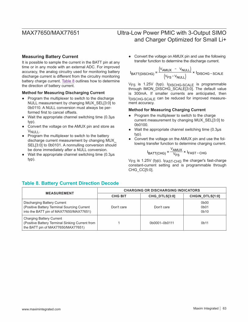
Measuring Battery CurrentIt is possible to sample the current in the BATT pin at any time or in any mode with an external ADC. For improved accuracy, the analog circuitry used for monitoring battery discharge current is different from the circuitry monitoring battery charge current. Table 8 outlines how to determine the direction of battery current.
Method for Measuring Discharging Current Program the multiplexer to switch to the discharge
NULL measurement by changing MUX_SEL[3:0] to 0b0110. A NULL conversion must always be per-formed first to cancel offsets.
Wait the appropriate channel switching time (0.3μs typ).
Convert the voltage on the AMUX pin and store as VNULL.
Program the multiplexer to switch to the battery discharge current measurement by changing MUX_SEL[3:0] to 0b0101. A nonnulling conversion should be done immediately after a NULL conversion.
Wait the appropriate channel switching time (0.3μs typ).
Convert the voltage on AMUX pin and use the following transfer function to determine the discharge current.
IBATT(DISCHG) =(VAMUX − VNULL)
(VFS −VNULL)× IDISCHG−SCALE
VFS is 1.25V (typ). IDISCHG-SCALE is programmable through IMON_DISCHG_SCALE[3:0]. The default value is 300mA. If smaller currents are anticipated, then IDISCHG-SCALE can be reduced for improved measure-ment accuracy.
Method for Measuring Charging Current Program the multiplexer to switch to the charge
current measurement by changing MUX_SEL[3:0] to 0b0100.
Wait the appropriate channel switching time (0.3μs typ).
Convert the voltage on the AMUX pin and use the fol-lowing transfer function to determine charging current.
IBATT(CHG) =VAMUXVFS
× IFAST −CHG
VFS is 1.25V (typ). IFAST-CHG the charger's fast-charge constant-current setting and is programmable through CHG_CC[5:0].
MEASUREMENTCHARGING OR DISCHARGING INDICATORS
CHG BIT CHG_DTLS[3:0] CHGIN_DTLS[1:0]
Discharging Battery Current (Positive Battery Terminal Sourcing Current into the BATT pin of MAX77650/MAX77651)
Don't care Don't care0b000b010b10
Charging Battery Current (Positive Battery Terminal Sinking Current from the BATT pin of MAX77650/MAX77651)
1 0b0001–0b0111 0b11
Table 8. Battery Current Direction Decode
www.maximintegrated.com Maxim Integrated 63
MAX77650/MAX77651 Ultra-Low Power PMIC with 3-Output SIMO and Charger Optimized for Small Li+

SIMO Buck-BoostThe device has a micropower single-inductor, multiple-out-put (SIMO) buck-boost DC-to-DC converter designed for applications that emphasize low supply current and small solution size. A single inductor is used to regulate three separate outputs, saving board space while delivering better total system efficiency than equivalent power solu-tions using one buck and linear regulators.The SIMO configuration utilizes the entire battery voltage range due to its ability to create output voltages that are above, below, or equal to the input voltage. Peak induc-tor current for each output is programmable to optimize the balance between efficiency, output ripple, EMI, PCB design, and load capability.
SIMO Benefits and Features 3 Output Channels Ideal for Low-Power Designs
• Delivers > 300mA at 1.8V from a 3.7V Input• ±3% Accurate Output Voltage
Small Solution Size• Multiple Outputs from a Single 1.5μH (0603) Inductor• Small 10μF (0402) Output Capacitors
Flexible and Easy to Use• Single Mode of Operation• Programmable Peak Inductor Current• Programmable On-Chip Active Discharge
Long Battery Life• High Efficiency, > 87% at 3.3V Output• Better Total System Efficient than Buck + LDOs• Low Quiescent Current, 1μA per Output• Low Input Operating Voltage, 2.7V (min)
Figure 18. SIMO Detailed Block Diagram
1.5µH
LXB
10µF(0402)
3300pF(0201)
PGND
10µF(0402)
REVERSE BLOCKING
SBB0
DIGITAL AND REGISTERS
CNFG_SBB_TOP, CNFG_SBBX_A, CNFG_SBBX_B
SIMOCONTROLLER
/
M1
M2 M4
LXA
ILIM
IZX
DRV_SBB
SYNCHRONOUS RECTIFIER
BST
DRV_SBBCHGDIS
SYNCHRONOUS RECTIFIER (M3_1)
ANDERROR COMPARATOR
ANDACTIVE-DISCHARGE
DRV_SBBBST
DIS_SBB1
DIS_SBB1
10µF(0402)
SBB1
ERROR COMPARATORREG0
REG1
SYNCHRONOUS RECTIFIER (M3_2)
ANDERROR COMPARATOR
ANDACTIVE-DISCHARGE
DRV_SBBBST
DIS_SBB2
10µF(0402)
SBB2
REG2
ACTIVE-DISCHARGE
AD_SBB0
AD_SBB1
AD_SBB2
MAIN POWER STAGE
I.ZXI.LIM CHG
DISDIS_SBB[2:0]REG[2:0]
DRV_SBBCOMM
VREF
SYS IN_SBB
BSTIN_SBB
M3_0
AD_SBB[2:0]
RAD_SSB0(140Ω)
FPS
VIREF
SYS_RST
MAX77650/MAX77651
www.maximintegrated.com Maxim Integrated 64
MAX77650/MAX77651 Ultra-Low Power PMIC with 3-Output SIMO and Charger Optimized for Small Li+

SIMO Control SchemeThe SIMO buck-boost is designed to service multiple out-puts simultaneously. A proprietary controller ensures that all outputs get serviced in a timely manner, even while multiple outputs are contending for the energy stored in the inductor. When no regulator needs service, the state machine rests in a low-power rest state.When the controller determines that a regulator requires service, it charges the inductor (M1 + M4) until the peak current limit is reached (ILIM = IP_SBB). The inductor energy then discharges (M2 + M3_x) into the output until the current reaches zero (IZX). In the event that multiple output channels need servicing at the same time, the con-troller ensures that no output utilizes all of the switching cycles. Instead, cycles interleave between all the outputs that are demanding service, while outputs that do not need service are skipped.
SIMO Soft-StartThe soft-start feature of the SIMO limits inrush current dur-ing startup. The soft-start feature is achieved by limiting the slew rate of the output voltage during startup (dV/dtSS).More output capacitance results in higher input current surges during startup. The following set of equations and example describes the input current surge phenomenon during startup.The current into the output capacitor (ICSBB) during soft-start is:
ICSBB = CSBBdV
dtSS(Equation 1)
where CSBB is the capacitance on the output of the regula-tor, and dV/dtSS is the voltage change rate of the output.The input current (IIN) during soft-start is:
IIN =(ICSBB + ILOAD)
VSBBxVIN
ξ (Equation 2)
where ICSBB is from the calculation above, ILOAD is cur-rent consumed from the external load, VSBBx is the output voltage, and VIN is the input voltage, ξ is the efficiency of the regulator.
For example, given the following conditions, the peak input current (IIN) during soft-start is ~71mA:Given:
VIN is 3.5V VSBB2 is 3.3V CSBB2 = 10µF dV/dtSS = 5mV/µs RLOAD2 = 330Ω (ILOAD2 = 3.3V/330Ω = 10mA) ξ is 80%
Calculation: ICSBB = 10µF x 5mV/µs (from Equation 1) ICSBB = 50mA
IIN =(50mA+ 10mA)3.3V3.5V
0.85 (from Equation1) IIN ~ 71mA
SIMO RegistersEach SIMO buck-boost channel has a dedicated register to program its target output voltage (TV_SBBx) and its peak current limit (IP_SBBx). Additional controls are avail-able for enabling/disabling the active discharge resistors (ADE_SBBx), as well as enabling/disabling the SIMO buck-boost channels (EN_SBBx). For a full description of bits, registers, default values, and reset conditions, refer to the Programmer’s Guide.
SIMO Active Discharge ResistanceEach SIMO buck-boost channel has an active-discharge resistor (RAD_SBBx) that is automatically enabled/dis-abled based on a ADE_SBBx and the status of the SIMO regulator. The active discharge feature can be enabled (ADE_SBBx = 1) or disabled (ADE_SBBx = 0) indepen-dently for each SIMO channel. Enabling the active dis-charge feature helps ensure a complete and timely power down of all system peripherals. If the active-discharge resistor is enabled by default, then the active-discharge resistor is on whenever VSYS is below VSYSUVLO and above VPOR.These resistors discharge the output when ADE_SBBx = 1, and their respective SIMO channel is off. Note if the regulator is forced on through EN_SBBx = 0b110 or 0b111, then the resistors do not discharge the output even if the regulator is disabled by the main-bias.Note that when VSYS is less than 1.0V, the NMOS transis-tors that control the active discharge resistors lose their gate drive and become open.
www.maximintegrated.com Maxim Integrated 65
MAX77650/MAX77651 Ultra-Low Power PMIC with 3-Output SIMO and Charger Optimized for Small Li+

SIMO Applications InformationSIMO Available Output CurrentThe available output current on a given SIMO channel is a function of the input voltage, output voltage, peak cur-rent limit setting, and the output current of the other SIMO channels. Maxim offers a SIMO calculator that outlines the available capacity for specific conditions. See Support Materials for more information on this and other engineer-ing resources. Table 9 is an extraction from the calculator.
Inductor SelectionChoose an inductance from 1.0μH to 2.2uH; 1.5μH induc-tors work best for most designs. Larger inductances transfer more energy to the output for each cycle and typically result in larger output voltage ripple and better efficiency. See the Output Capacitor Selection section for more information on how to size your output capacitor in order to control ripple.
Choose the inductor saturation current to be greater than or equal to the maximum peak current limit setting that is used for all of the SIMO buck-boost channels (IP_SBB). For example, if SBB0 is set for 0.5A, SBB1 is set for 0.866A, and SBB2 is set for 1.0A, then choose the satura-tion current to be greater than or equal to 1.0A.Choose the RMS current rating of the inductor (typically the current at which the temperature rises appreciably) based on the expected load currents for the system. For systems where the expected load currents are not well known, be conservative and choose the RMS current to be greater than or equal to the half of higher maximum peak current limit setting [IRMS>=MAX(IP_SBB0, IP_SBB1, IP_SBB2)/2]. This is a safe/conservative choice because the SIMO buck-boost regulator implements a discontinuous conduction mode (DCM) control scheme, which returns the inductor current to zero each cycle.Consider the DC-resistance (DCR), AC-resistance (ACR) and solution size of the inductor. Typically, smaller sized inductors have larger DC-resistance and larger AC-resistance that reduces efficiency and the available output current. Note that many inductor manufacturers have inductor families which contain different versions of core material in order to balance trade-offs between DCR, ACR (i.e., core losses), and component cost. For this SIMO regulator, inductors with the lowest ACR in the 1.0MHz to 2.0MHz region tend to provide the best efficiency.See Table 10 for examples of inductors that work well with this device. This table was generated in the middle of 2016 and the highest efficiency inductors are listed first. Inductor technology advances rapidly and by the end of 2017 this table may no longer represent the best market offerings.
PARAMETERS EXAMPLE 1 EXAMPLE 2 EXAMPLE 3V.IN.MIN 2.7V 3.2V 3.4VR.L.DCR 0.1Ω 0.1Ω 0.12Ω
SBB1 1V at 100mA 1.2V at 50mA 1.2V at 20mA
SBB0 1.2V at 75mA 2.05V at 100mA 2.05V at 80mA
SBB2 1.8V at 50mA 3.3V at 30mA 3.3V at 10mAI.PEAK.0 1A 0.866A 0.5AI.PEAK.1 1A 0.707A 0.5AI.PEAK.2 1A 1A 0.5AUtilized
Capacity 79 76 73
*R.C.IN = R.C.OUT = 5mΩ, L = 1.5μH
Table 9. SIMO Available Output Current for Common Applications
MANUFACTURER PART L (µH) ISAT (A) IRMS (A) DCR (Ω) X (mm) Y (mm) Z (mm)Samsung CIGT201610EH2R2MN 2.2 2.9 2.7 0.073 2.0 1.6 1.0Murata DFE201610E-2R2M 2.2 2.6 1.9 0.117 2.0 1.6 1.0Murata DFE201610E-1R5M 1.5 2.4 3.2 0.076 2.0 1.6 1.0Murata DFE201210S-2R2M 2.2 2.3 1.80 0.127 2.0 1.2 1.0Murata DFE201210S-1R5M 1.5 2.2 2.6 0.086 2.0 1.2 1.0Samsung CIGT201208EH2R2MN 2.2 2.0 1.8 0.095 2.0 1.25 0.8Murata DFE201208S-1R5M 1.5 2.4 2.0 0.110 2.0 1.2 0.8Murata DFE201208S-2R2M 2.2 2.0 1.6 0.170 2.0 1.2 0.8
Table 10. Example Inductors
www.maximintegrated.com Maxim Integrated 66
MAX77650/MAX77651 Ultra-Low Power PMIC with 3-Output SIMO and Charger Optimized for Small Li+

Input Capacitor SelectionChoose the input bypass capacitance (CIN_SBB) to be 10µF. Larger values of CIN_SBB improve the decoupling for the SIMO regulator.CIN_SBB reduces the current peaks drawn from the battery or input power source during SIMO regulator operation and reduces switching noise in the system. The ESR/ESL of the input capacitor should be very low (i.e., ≤ 5mΩ + ≤ 500pH) for frequencies up to 2MHz. Ceramic capacitors with X5R or X7R dielectric are highly recommended due to their small size, low ESR, and small temperature coefficients.To fully utilize the available input voltage range of the SIMO (5.5V max), use a 6.3V capacitor voltage rating.IN_SBB is a critical discontinuous current path that requires careful bypassing. When the SIMO detects that an output is below its regulation threshold, a switching cycle begins and the IN_SBB current ramps up as a func-tion of the input voltage and inductor (di/dt = VIN_SBB/L) until it reaches the peak current limit (IP_SBB). Once IP_SBB is reached, the IN_SBB current falls to zero rapidly (~5ns). This rapid current decrease makes the parasitic inductance in the PGND to input capacitor to IN_SBB path critical. In the PCB layout, place CIN_SBB as close as possible to the power pins (IN_SBB and PGND) to minimize parasitic inductance. If making connections to the input capacitor through vias, ensure that the vias are rated for the expected input current so they do not contribute excess inductance and resistance between the bypass capacitor and the power pins.
Boost Capacitor SelectionChoose the boost capacitance (CBST) to be 3.3nF. Smaller values of CBST (< 1nF) result in insufficient gate drive for M3. Larger values of CBST (> 10nF) have the potential to degrade the startup performance. Ceramic capacitors with 0201 or 0402 case size are recommended.
Output Capacitor SelectionChoose each output bypass capacitance (CSBBx) based on the desired output voltage ripple; typical values are 10µF. Larger values of CSBBx improve the output volt-age ripple but increase the input surge currents during soft-start and output voltage changes. The output voltage ripple is a function of the inductance, the output voltage, and the peak current limit setting. Maxim offers a SIMO calculator to aid in the selection of the output capacitance. See Support Materials for more information on this and other engineering resources.
Note that most designs concern themselves with having enough capacitance on the output but there is also a maximum capacitance limitation that is calculated within the SIMO Calculator; take care not to exceed the maxi-mum capacitance.CSBBx is required to keep the output voltage ripple small. The impedance of the output capacitor (ESR, ESL) should be very low (i.e., ≤ 5mΩ + ≤ 500pH) for frequencies up to 2MHz. Ceramic capacitors with X5R or X7R dielectric are highly recommended due to their small size, low ESR, and small temperature coefficients.A capacitor's effective capacitance decreases with increased DC bias voltage. This effect is more pro-nounced as capacitor case sizes decrease. Due to this characteristic, it is possible for an 0603 case size capaci-tor to perform well, while an 0402 case size capacitor of the same value performs poorly. The SIMO regulator is stable with low output capacitance (1μF) but the output voltage ripple would be large; consider the effective out-put capacitance value after initial tolerance, bias voltage, aging, and temperature derating.SBBx is a critical discontinuous current path that requires careful bypassing. When the SIMO detects that an output is below its target, it charges the inductor to a peak cur-rent limit (IP_SBB) and then discharges that inductor into the output. At the moment the charge is applied to the output, the current increases rapidly and then decays relatively slowly (dt/dt = VOUT/L). This rapid current increase is a function of the drive strength setting (DRV_SBB) and makes the parasitic inductance in the SBBx to output capacitor to PGND path critical. In the PCB layout, place CSBBx as close as possible to SBBx and PGND to minimize parasitic inductance. If making connections to the output capacitor through vias, ensure that the vias are rated for the expected output current so they do not contribute excess inductance and resistance.
SIMO Switching FrequencyThe SIMO buck-boost regulator utilizes a pulse frequency modulation (PFM) control scheme. The switching fre-quency for each output is a function of the input voltage, output voltage, load current, and inductance. Maxim offers a SIMO calculator to aid in the understanding of the switching frequency.
www.maximintegrated.com Maxim Integrated 67
MAX77650/MAX77651 Ultra-Low Power PMIC with 3-Output SIMO and Charger Optimized for Small Li+

At no load, switching frequencies can be as low as 10Hz. It is possible to get SIMO switching frequencies that are high (5.7MHz) with all of the worst-case conditions: high input voltage (4.5V), low inductance (1.0µH), high output voltage (5.0V), low peak current limit (0.5A), and high utilization (80% which is 90mA with these conditions). With these high switching frequencies, the SIMO effi-ciency is poor. The maximum switching frequencies for designs should be no more than 3MHz. For example, in the 5.7MHz example above if we change the inductance to peak current limit from 0.5A to 0.707A while leaving the load current at 90mA, then the switching frequency drops to 2.4MHz. If we put the peak current limit at 0.866A and change the inductance to 1.5µH, then the switching fre-quency drops to 1MHz which provides a “nice” efficiency.
Unused OutputsDo not leave unused outputs unconnected. If an output left unconnected is accidentally enabled, inductor current dumps into an open pin, and the output voltage can soar above the absolute maximum rating, potentially causing damage to the device. If the unused output is always disabled (EN_SBBx = 0x4 or 0x5), connect that output to ground. If an unused output can be enabled at any point during operation (such as startup or accidental software access), then implement one of the following:
Bypass the unused output with a 1µF ceramic capacitor to ground.
Connect the unused output to the power input (IN_SBB). This connection is beneficial because it does not require an external component for the unused output. The power input and its capacitance receives the energy packets when the regulator is enabled and VIN_SBB is below the target output voltage of the unused output. Circulating the energy back to the power input ensures that the unused output voltage does not fly high.• Note that some OTP options of the device have the
active-discharge resistors enabled by default (ADE_SBBx) such that connecting an unused output SBBx to IN_SBB creates a 140Ω (RAD_SBBx) to ground until software can be ran to disable the active-dis-charge resistor. Connecting an unused SBBx to IN_SBB is not recommended if the regulator's active-discharge resistor is enabled by default.
Connect the unused output to another power output that is above the target voltage of the unused output. In the same way as the option listed above, this con-nection is beneficial because it does not require an
external component for the unused output. Unlike the option above, this connection is preferred in cases where the unused output voltage bias level is always above the unused output voltage target because no energy packages are provided to the unused output.• Note that some OTP options of the device have the
active-discharge resistors enabled by default (ADE_SBBx). If the other power output used to bias the unused output is normally off, then the active-dis-charge resistor of the unused output does not cre-ate a continuous current draw. Remember that once the system is enabled, it should turn off the unused output's active-discharge resistor (ADE_SBBx = 0).
LDOThe device includes one on-chip low-dropout linear regu-lator (LDO). This LDO is optimized to have low-quiescent current and low dropout voltage. The input voltage range of this LDO (VIN_LDO) allows it to be powered directly from the main energy source such as a Li-Poly battery or from an intermediate regulator. The linear regulator deliv-ers up to 150mA.
Features 150mA LDO 1.8V to 5.5V Input Volage Range Adjustable Output Voltage 180mV Maximum Dropout Voltage Programmable On-Chip Active Discharge
LDO Simplified Block DiagramThe LDO has one input (IN_LDO) and one output (LDO) and several ports that exchange information with the rest of the device (VREF, EN_LDO, ADE_LDO). VREF comes from the main bias circuits. EN_LDO and ADE_LDO are register bits for controlling the enable and active-discharge feature of the LDO. Refer to the Programmer’s Guide for more information.
LDO Active Discharge ResistorThe LDO has an active-discharge resistor (RAD_LDO) that automatically enables/disables based on a configura-tion bit (ADE_LDO) and the status of the LDO regulator. Enabling the active discharge feature helps ensure a complete and timely power down of all system peripherals. The default condition of the active-discharge resistor fea-ture is enabled such that whenever VSYS is above VPOR and VIN_LDO is above 1.0V, the LDO active discharge resistor is turned on. Note that when VIN_LDO is less than 1.0V, the NMOS transistor that controls the LDO active discharge resistor loses its gate drive and becomes open.
www.maximintegrated.com Maxim Integrated 68
MAX77650/MAX77651 Ultra-Low Power PMIC with 3-Output SIMO and Charger Optimized for Small Li+
LDO Soft-StartThe soft-start feature of the LDO limits inrush current dur-ing startup. The soft-start feature is achieved by limiting the slew rate of the output voltage during startup (dV/dtSS).More output capacitance results in higher input cur-rent surges during startup. The equation and example describes the input current surge phenomenon during startup.The input current (IIN) during soft-start is:
IIN = CLDOdVdtSS
+ ILDO
where CLDO is the capacitance on the output of the regula-tor, and dV/dtSS is the voltage change rate of the output. For example, given the following conditions, the input current (IIN) during soft-start is 22.5mA:Given:
• CLDO = 10µF• dV/dtSS = 1.25mV/µs• RLDO = 185Ω (ILDO = 1.85V/185Ω = 10mA)
Calculation:• IIN = 10µF x 1.25mV/µs + 10mA• IIN = 22.5mA
LDO Applications InformationInput and Output Capacitor SelectionSufficient input bypass capacitance (CIN_LDO) and output capacitance (CLDO) is required for stable operation of the LDO. Figure 19 provides guidance on capacitor selection and refers to required effective capacitance, which is the actual value of capacitance seen by the LDO during oper-ation. Effective capacitance is almost always lower than the nominal capacitance and is a commonly overlooked design parameter. Determine the effective capacitance by assessing the capacitor’s initial tolerance, variation with temperature, and variation with DC bias. Consult the capacitor manufacturer for specific details of derating.Choose the input capacitor (CIN_LDO) so that the effective capacitance is equal to or greater than the value found in Figure 19, based on expected load conditions for the application. A single 10μF, 1005/0402 (mm/inch) capaci-tor, is recommended for typical applications but ensure that the load current and derated capacitance does not compromise the stability curve in Figure 19. Larger values of CIN_LDO improve stability and decoupling for the LDO regulator. The floorplan of the device is such that SBB0 is adjacent to IN_LDO, and if SBB0 powers the input of
the LDO, then the two nodes can share the SBB0 output capacitor (CSBB0). CIN_LDO reduces the current peaks drawn from the battery or input power source during LDO regulator operation.Choose the output capacitor (CLDO) so that the effective capacitance is equal to or greater than the value found in Figure 19, based on expected load conditions for the application. A single 10μF, 1005/0402 (mm/inch) capacitor is recommended for typical applications, but ensure that the load current and derated capacitance does not com-promise the stability curve in Figure 19. Larger values of CLDO improve stability and output PSRR, but increases the input surge currents during soft-start and output volt-age changes. The effective output capacitance should not exceed 100μF to maintain LDO stability.For example, consider the case of the MAX77650A where:
1. Size is very important.2. The LDO input is powered by SBB0, which is 2.05V.3. The LDO output is 1.85V.4. The LDO output current is ≤80mA.
A small 1005/0402 (mm/inch) capacitor such as the GRM155R60J106ME15 (Murata, 10μF, 6.3V X5R) gives 5.7μF at 60°C and 5.4μF at -20°C with the 1.85V bias voltage and has a ± 20% tolerance, so the worst-case effective capacitance is 4.3μF (5.4μF derated by 20% tolerance). With just 4.3μF of capacitance at the output, Figure 19 shows the LDO is stable with load currents of ≤35mA. To get stability at 80mA, 6μF is required. There are a few options to consider:
Add more capacitors to the design. Replace the 1005/0402 (mm/inch) capacitor with a
1608/0603 (mm/inch) capacitor. Consider point-of-load capacitance in your assess-
ment of effective capacitance. For example, if there is a point-of-load capacitor downstream from the LDO that is sufficiently close to the local LDO output capacitor, it can cover the gap. The capacitor can be considered “sufficiently close” if the PCB does not add more than 25nH and 25mΩ of extra ESR and ESL (more or less within 1”).
Note the impedance of either the input or output capacitor (ESR, ESL) should be very low (i.e., ≤ 50mΩ + ≤ 5nH) for frequencies up to 0.5MHz. Ceramic capacitors with X5R or X7R dielectric are highly recommended due to their small size, low ESR, and small temperature coefficients.
www.maximintegrated.com Maxim Integrated 69
MAX77650/MAX77651 Ultra-Low Power PMIC with 3-Output SIMO and Charger Optimized for Small Li+
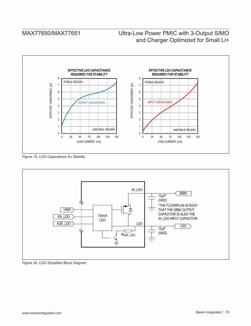
Figure 20. LDO Simplified Block Diagram
Figure 19. LDO Capacitance for Stability
0
1
2
3
4
5
6
7
8
0 25 50 75 100 125 150
EFFE
CTIV
E CA
PACI
TANC
E (μF
)
LOAD CURRENT (mA)
OUTPUT CAPACITANCE
EFFECTIVE LDO CAPACITANCE REQUIRED FOR STABILITY
UNSTABLE REGION
STABLE REGION
0
1
2
3
4
5
6
7
8
0 25 50 75 100 125 150EF
FECT
IVE
CAPA
CITA
NCE
(μF)
LOAD CURRENT (mA)
INPUT CAPACITANCE
EFFECTIVE LDO CAPACITANCE REQUIRED FOR STABILITY
STABLE REGION
UNSTABLE REGION
IN_LDO
LDO
10µF*(0402)
10µF(0402)
150mA LDO
VREF
EN_LDO
ADE_LDO
RADE_LDO
LDO
SBB0
*THE FLOORPLAN IS SUCH THAT THE SBB0 OUTPUT CAPACITOR IS ALSO THE IN_LDO INPUT CAPACITOR.
www.maximintegrated.com Maxim Integrated 70
MAX77650/MAX77651 Ultra-Low Power PMIC with 3-Output SIMO and Charger Optimized for Small Li+

Current SinksThe device has a 3-channel current sink driver designed to drive LED's in portable devices. This block can also be used as a general-purpose current sink driver for other applications. The driver's on-time and frequency are independently programmable for each output to achieve a desired blink pattern. Alternatively, the LEDs can be continuously on (i.e., not blinking). The blink period is programmable from 0.5s to 8s,with an on-time duty cycle from 6.25% to 100%.Figure 21 utilizes a common set of clock dividers to drive three identical current sink modules. Refer to the Programmer’s Guide for more information.
Current Sink Applications InformationLED AssignmentThe three current sinks (LED0, LED1, LED2) are identi-cal. In a typical application where a red, green, blue LED cluster is used (RGB), the assignment of the RGB ele-ments to the LED0/1/2 pins should be done in whatever way makes the PCB layout the easiest.
Unused Current Sink PortsIf a current sink port is not utilized in a given applica-tion, connect that port to ground. Additionally, software should ensure that the unused current sink is not enabled (EN_LEDx = 0).
Figure 21. Current Sink Block Diagram
LED0
LED1
LED2
LGND
D_LED0[3:0]P_LED0[3:0]INV_LED0
BRT_LED0[4:0]
2/4/8Ω CLK_32
EN_LED0
LED_FS0[1:0]
BIAS
CLOCK DIVIDER AND INVERTEREN_LED_MSTR
CURRENT SINK
D_LED1[3:0]P_LED1[3:0]INV_LED0
BRT_LED1[4:0]
CLK_32LED_FS1[1:0]
CURRENT SINK
D_LED2[3:0]P_LED2[3:0]INV_LED0
BRT_LED24:0]
CLK_32LED_FS2[1:0]
CURRENT SINK
CLK CLOCK DIVIDER CLK_64 CLK_32
CLK_64_S
PWM LOGIC
DAC
www.maximintegrated.com Maxim Integrated 71
MAX77650/MAX77651 Ultra-Low Power PMIC with 3-Output SIMO and Charger Optimized for Small Li+

I2CThe MAX77650 features a revision 3.0 I2C-compatible, 2-wire serial interface consisting of a bidirectional serial data line (SDA) and a serial clock line (SCL). The MAX77650/MAX77651 act as slave-only devices where they rely on the master to generate a clock signal. SCL clock rates from 0Hz to 3.4MHz are supported. I2C is an open-drain bus, and therefore, SDA and SCL require pullups. Optional resistors (24Ω) in series with SDA and SCL protect the device inputs from high-voltage spikes on the bus lines. Series resistors also minimize crosstalk and undershoot on bus signals. Figure 22 shows the
functional diagram for the I2C based communications controller. For additional information on I2C, refer to the I2C Bus Specification and User Manual that is available for free on the Internet.Features
I2C Revision 3 Compatible Serial Communications Channel
0Hz to 100kHz (Standard Mode) 0Hz to 400kHz (Fast Mode) 0Hz to 1MHz (Fast Mode Plus) 0Hz to 3.4MHz (High-Speed Mode) Does not utilize I2C Clock Stretching
Figure 22. I2C Simplified Block Diagram
SCL
SDA
INTERFACE DECODERS
SHIFT REGISTERSBUFFERS
PERIPHERAL 0
PERIPHERAL 1
PERIPHERAL 2
PERIPHERAL N-1
PERIPHERAL N
COMMUNICATIONS CONTROLLER
COM
VIO
GND
www.maximintegrated.com Maxim Integrated 72
MAX77650/MAX77651 Ultra-Low Power PMIC with 3-Output SIMO and Charger Optimized for Small Li+
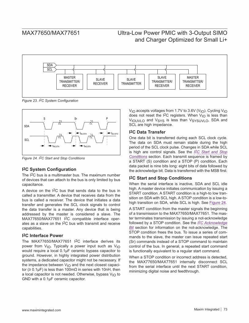
I2C System ConfigurationThe I2C bus is a multimaster bus. The maximum number of devices that can attach to the bus is only limited by bus capacitance.A device on the I2C bus that sends data to the bus in called a transmitter. A device that receives data from the bus is called a receiver. The device that initiates a data transfer and generates the SCL clock signals to control the data transfer is a master. Any device that is being addressed by the master is considered a slave. The MAX77650/MAX77651 I2C compatible interface oper-ates as a slave on the I2C bus with transmit and receive capabilities.
I2C Interface PowerThe MAX77650/MAX77651 I2C interface derives its power from VIO. Typically a power input such as VIO would require a local 0.1μF ceramic bypass capacitor to ground. However, in highly integrated power distribution systems, a dedicated capacitor might not be necessary. If the impedance between VIO and the next closest capaci-tor (≥ 0.1μF) is less than 100mΩ in series with 10nH, then a local capacitor is not needed. Otherwise, bypass VIO to GND with a 0.1µF ceramic capacitor.
VIO accepts voltages from 1.7V to 3.6V (VIO). Cycling VIO does not reset the I2C registers. When VIO is less than VIOUVLO and VSYS is less than VSYSUVLO, SDA and SCL are high impedance.
I2C Data TransferOne data bit is transferred during each SCL clock cycle. The data on SDA must remain stable during the high period of the SCL clock pulse. Changes in SDA while SCL is high are control signals. See the I2C Start and Stop Conditions section. Each transmit sequence is framed by a START (S) condition and a STOP (P) condition. Each data packet is nine bits long: eight bits of data followed by the acknowledge bit. Data is transferred with the MSB first.
I2C Start and Stop ConditionsWhen the serial interface is inactive, SDA and SCL idle high. A master device initiates communication by issuing a START condition. A START condition is a high-to low tran-sition on SDA with SCL high. A STOP condition is a low-to-high transition on SDA, while SCL is high. See Figure 24.A START condition from the master signals the beginning of a transmission to the MAX77650/MAX77651. The mas-ter terminates transmission by issuing a not-acknowledge followed by a STOP condition. See the I2C Acknowledge Bit section for information on the not-acknowledge. The STOP condition frees the bus. To issue a series of com-mands to the slave, the master can issue repeated start (Sr) commands instead of a STOP command to maintain control of the bus. In general, a repeated start command is functionally equivalent to a regular start command.When a STOP condition or incorrect address is detected, the MAX77650/MAX77651 internally disconnect SCL from the serial interface until the next START condition, minimizing digital noise and feedthrough.
Figure 23. I2C System Configuration
Figure 24. I2 C Start and Stop Conditions
SLAVETRANSMITTER/
RECEIVER
SLAVETRANSMITTER
SLAVERECEIVER
MASTERTRANSMITTER/
RECEIVER
MASTERTRANSMITTER/
RECEIVER
SDASCL
S PSr
SCL
SDA
tHD;STA
tSU;STA tSU;STO
tHD;STA
www.maximintegrated.com Maxim Integrated 73
MAX77650/MAX77651 Ultra-Low Power PMIC with 3-Output SIMO and Charger Optimized for Small Li+

I2C Acknowledge BitBoth the I2C bus master and the MAX77650/MAX77651 (slave) generate acknowledge bits when receiving data. The acknowledge bit is the last bit of each nine bit data packet. To generate an acknowledge (A), the receiving device must pull SDA low before the rising edge of the acknowledge-related clock pulse (ninth pulse) and keep it low during the high period of the clock pulse. See Figure 25. To generate a not-acknowledge (nA), the receiving device allows SDA to be pulled high before the rising edge of the acknowledge-related clock pulse and leaves it high during the high period of the clock pulse.Monitoring the acknowledge bits allows for detection of unsuccessful data transfers. An unsuccessful data transfer occurs if a receiving device is busy or if a system
fault has occurred. In the event of an unsuccessful data transfer, the bus master should reattempt communication at a later time.The MAX77650/MAX77651 issue an ACK for all register addresses in the possible address space even if the par-ticular register does not exist.
I2C Slave AddressThe I2C controller implements 7-bit slave addressing. An I2C bus master initiates communication with the slave by issuing a START condition followed by the slave address. See Figure 26. The OTP address is factory programmable for one of two options. See Table 11. All slave addresses not mentioned in the Table 11 are not acknowledged.
Figure 26. Slave Address Example
Figure 25. Acknowledge Bit
tSU;DAT
S
SCL
SDA
1 2 8 9
tHD;DAT
NOT ACKNOWLEDGE (NA)ACKNOWLEDGE (A)
S
SCL
SDA
1 2 3
001
8 9
ACKNOWLEDGE
4 5 6 7
1 0 0 R/W A0
www.maximintegrated.com Maxim Integrated 74
MAX77650/MAX77651 Ultra-Low Power PMIC with 3-Output SIMO and Charger Optimized for Small Li+

I2C Clock StretchingIn general, the clock signal generation for the I2C bus is the responsibility of the master device. The I2C specifica-tion allows slow slave devices to alter the clock signal by holding down the clock line. The process in which a slave device holds down the clock line is typically called clock stretching. The MAX77650/MAX77651 do not use any form of clock stretching to hold down the clock line.
I2C General Call AddressThe MAX77650/MAX77651 do not implement the I2C specifications general call address. If the MAX77650/MAX77651 see the general call address (0b0000_0000), they do not issue an acknowledge.
I2C Device IDThe MAX77650/MAX77651 do not support the I2C Device ID feature.
I2C Communication SpeedThe MAX77650/MAX77651 are compatible with all 4 com-munication speed ranges as defined by the Revision 3 I2C specification:
0Hz to 100kHz (Standard Mode) 0Hz to 400kHz (Fast Mode) 0Hz to 1MHz (Fast Mode) 0Hz to 3.4MHz (High-Speed Mode)
Operating in standard mode, fast mode, and fast mode plus does not require any special protocols. The main consideration when changing the bus speed through this range is the combination of the bus capacitance and
pullup resistors. Higher time constants created by the bus capacitance and pullup resistance (C x R) slow the bus operation. Therefore, when increasing bus speeds, the pullup resistance must be decreased to maintain a rea-sonable time constant. Refer to the Pullup Resistor Sizing section of the I2C Bus Specification and User Manual that is available for free on the Internet for detailed guid-ance on the pullup resistor selection. In general for bus capacitances of 200pF, a 100kHz bus needs 5.6kΩ pullup resistors, a 400kHz bus needs about a 1.5kΩ pullup resis-tors, and a 1MHz bus needs 680Ω pullup resistors. Note that when the open-drain bus is low, the pullup resistor is dissipating power, lower value pullup resistors dissipate more power (V2/R).Operating in high-speed mode requires some special con-siderations. For a full list of considerations, see the I2C Communication Speed section. The major considerations with respect to the MAX77650/MAX77651:
The I2C bus master use current source pull-ups to shorten the signal rise.
The I2C slave must use a different set of input filters on its SDA and SCL lines to accommodate for the higher bus.
The communication protocols need to utilize the high-speed master code.
At power-up and after each stop condition, the MAX77650/MAX77651 input filters are set for standard mode, fast mode, and fast mode plus (i.e., 0Hz to 1MHz). To switch the input filters for high-speed mode, use the high-speed master code protocols that are described in the I2C Communication Protocols section.
ADDRESS 7-BIT SLAVE ADDRESS 8-BIT WRITE ADDRESS 8-BIT READ ADDRESSMain Address(ADDR = 1)* 0x48, 0b 100 1000 0x90, 0b 1001 0000 0x91, 0b 1001 0001
Main Address(ADDR = 0)* 0x40, 0b 100 0000 0x80, 0b 1000 0000 0x81, 0b 1000 0001
Test Mode** 0x49, 0b 100 1001 0x92, 0b 1001 0010 0x93, 0b 1001 0011*Perform all reads and writes on the Main Address. ADDR is a factory one-time programmable (OTP) option, allowing for address changes in the event of a bus conflict. Contact Maxim for more information.**When test mode is unlocked, the additional address is acknowledged. Test mode details are confidential. If possible, leave the test mode address unallocated to allow for the rare event that debugging needs to be performed in cooperation with Maxim.
Table 11. I2C Slave Address Options
www.maximintegrated.com Maxim Integrated 75
MAX77650/MAX77651 Ultra-Low Power PMIC with 3-Output SIMO and Charger Optimized for Small Li+

I2C Communication ProtocolsThe MAX77650/MAX77651 supports both writing and reading from its registers.
Writing to a Single RegisterFigure 27 shows the protocol for the I2C master device to write one byte of data to the MAX77650/MAX77651. This protocol is the same as the SMBus specification’s write byte protocol.The write byte protocol is as follows:
The master sends a start command (S). The master sends the 7-bit slave address followed by
a write bit (R/W = 0).
The addressed slave asserts an acknowledge (A) by pulling SDA low.
The master sends an 8-bit register pointer. The slave acknowledges the register pointer. The master sends a data byte. The slave updates with the new data The slave acknowledges or not acknowledges
the data byte. The next rising edge on SDA loads the data byte into its target register and the data becomes active.
The master sends a stop condition (P) or a repeated start condition (Sr). Issuing a P ensures that the bus input filters are set for 1MHz or slower operation. Issuing an Sr leaves the bus input filters in their current state.
Figure 27. Writing to a Single Register with the Write Byte Protocol
1
S
NUMBER OF BITS
R/nW
SLAVE ADDRESS
7
0
1 8
REGISTER POINTERA
1
A
1 8
DATA A OR NA
1
P OR SR*
1
SLAVE TO MASTERMASTER TO SLAVE
LEGEND
8 9
ACKNOWLEDGE
7
B0 AB1
THE DATA IS LOADED INTO THE TARGET REGISTER AND BECOMES ACTIVE DURING THIS RISING EDGE.SDA
SCL *P FORCES THE BUS FILTERS TO SWITCH TO THEIR <=1MHZ MODE. SR LEAVES THE BUS FILTERS IN THEIR CURRENT STATE.
www.maximintegrated.com Maxim Integrated 76
MAX77650/MAX77651 Ultra-Low Power PMIC with 3-Output SIMO and Charger Optimized for Small Li+

Writing Multiple Bytes to Sequential RegistersFigure 28 shows the protocol for writing to a sequential registers. This protocol is similar to the write byte proto-col above, except the master continues to write after it receives the first byte of data. When the master is done writing it issues a stop or repeated start.The writing to sequential registers protocol is as follows:
The master sends a start command (S). The master sends the 7-bit slave address followed by
a write bit (R/W = 0). The addressed slave asserts an acknowledge (A) by
pulling SDA low. The master sends an 8-bit register pointer.
The slave acknowledges the register pointer. The master sends a data byte. The slave acknowledges the data byte. The next ris-
ing edge on SDA load the data byte into its target register and the data will become active.
Steps 6 to 7 are repeated as many times as the master requires.
During the last acknowledge related clock pulse, the master can issue an acknowledge or a not acknowledge.
The master sends a stop condition (P) or a repeated start condition (Sr). Issuing a P ensures that the bus input filters are set for 1MHz or slower operation. Issuing an Sr leaves the bus input filters in their current state.
Figure 28. Writing to Sequential registers X to N
1
S
NUMBER OF BITS
R/NW
SLAVE ADDRESS
7
0
1 8
REGISTER POINTER XA
1
A
1 8
DATA X A
1
NUMBER OF BITS8
DATA X+1 A
1 8
DATA X+2 A
1
NUMBER OF BITS8
DATA N-1 A
1 8
DATA N
SLAVE TO MASTERMASTER TO SLAVE
LEGEND
8 9
ACKNOWLEDGE
7
B0 AB1
THE DATA IS LOADED INTO THE TARGET REGISTER AND BECOMES ACTIVE DURING THIS RISING EDGE.
SDA
SCLDETAIL: Α
8 9
ACKNOWLEDGE
7
B0 AB1
THE DATA IS LOADED INTO THE TARGET REGISTER AND BECOMES ACTIVE DURING THIS RISING EDGE.
SDA
SCLDETAIL: Β
1
B9
Α
ΑΑ
Α Β
A OR NA
1P OR SR*
1
*P FORCES THE BUS FILTERS TO SWITCH TO THEIR <=1MHZ MODE. SR LEAVES THE BUS FILTERS IN THEIR CURRENT STATE.
REGISTER POINTER = X + 1 REGISTER POINTER = X + 2
REGISTER POINTER = X + (N-2) REGISTER POINTER = X + (N-1)
www.maximintegrated.com Maxim Integrated 77
MAX77650/MAX77651 Ultra-Low Power PMIC with 3-Output SIMO and Charger Optimized for Small Li+

Reading from a Single RegisterFigure 29 shows the protocol for the I2C master device to read one byte of data to the MAX77650/MAX77651. This protocol is the same as the SMBus specification’s read byte protocol. The read byte protocol is as follows:
The master sends a start command (S). The master sends the 7-bit slave address followed by
a write bit (R/W = 0). The addressed slave asserts an acknowledge (A) by
pulling SDA low. The master sends an 8-bit register pointer. The slave acknowledges the register pointer. The master sends a repeated start command (Sr). The master sends the 7-bit slave address followed by
a read bit (R/W = 1). The addressed slave asserts an acknowledge by
pulling SDA low.
The addressed slave places 8-bits of data on the bus from the location specified by the register pointer.
The master issues a not acknowledge (nA). The master sends a stop condition (P) or a repeated
start condition (Sr). Issuing a P ensures that the bus input filters are set for 1MHz or slower operation. Issuing an Sr leaves the bus input filters in their cur-rent state.
Note that when the MAX77650/MAX77651 receive a stop they do not modify their register pointer.
Reading from Sequential RegistersFigure 30 shows the protocol for reading from sequential registers. This protocol is similar to the read byte protocol except the master issues an acknowledge to signal the slave that it wants more data: when the master has all the data it requires it issues a not acknowledge (nA) and a stop (P) to end the transmission.
Figure 29. Reading from a Single Register with the Read Byte Protocol
Figure 30. Reading Continuously from Sequential Registers X to N
1
S
R/nW
SLAVE ADDRESS
7
0
1 8
REGISTER POINTER XA
1
A
1 1
Sr SLAVE ADDRESS
7
1
1 8
DATA XA
1
nA
1 NUMBER OF BITS
R/nW
SLAVE TO MASTERMASTER TO SLAVE
LEGEND
1
P or Sr*
*P FORCES THE BUS FILTERS TO SWITCH TO THEIR <=1MHZ MODE. SR LEAVES THE BUS FILTERS IN THEIR CURRENT STATE.
1
S
R/NW
SLAVE ADDRESS
7
0
1 8
REGISTER POINTER XA
1
A
1 1
SR SLAVE ADDRESS
7
1
1 8
DATA XA
1
A
1 NUMBER OF BITS
R/nW8
DATA X+3 A
1 NUMBER OF BITS8
DATA X+2 A
1
DATA X+1 A
8 1
8
DATA N NA
18
DATA N-1 A
1
DATA N-2 A
8 1
SLAVE TO MASTERMASTER TO SLAVE
LEGEND
NUMBER OF BITS1
P OR SR*
*P FORCES THE BUS FILTERS TO SWITCH TO THEIR <=1MHZ MODE. SR LEAVES THE BUS FILTERS IN THEIR CURRENT STATE.
REGISTER POINTER = X + 1 REGISTER POINTER = X + 2 REGISTER POINTER = X + 3
REGISTER POINTER = X + (N-3)
REGISTER POINTER = X + (N-2)
REGISTER POINTER = X + (N-1)
www.maximintegrated.com Maxim Integrated 78
MAX77650/MAX77651 Ultra-Low Power PMIC with 3-Output SIMO and Charger Optimized for Small Li+

The continuous read from sequential registers protocol is as follows:
The master sends a start command (S). The master sends the 7-bit slave address followed by
a write bit (R/W = 0). The addressed slave asserts an acknowledge (A) by
pulling SDA low. The master sends an 8-bit register pointer. The slave acknowledges the register pointer. The master sends a repeated start command (Sr). The master sends the 7-bit slave address followed
by a read bit (R/W = 1). When reading the RTC time-keeping registers, secondary buffers are loaded with the timekeeping register data during this operation.
The addressed slave asserts an acknowledge by pulling SDA low.
The addressed slave places 8-bits of data on the bus from the location specified by the register pointer.
The master issues an acknowledge (A) signaling the slave that it wishes to receive more data.
Steps 9 to 10 are repeated as many times as the master requires. Following the last byte of data, the master must issue a not acknowledge (nA) to signal that it wishes to stop receiving data.
The master sends a stop condition (P) or a repeated start condition (Sr). Issuing a stop (P) ensures that the bus input filters are set for 1MHz or slower opera-tion. Issuing an Sr leaves the bus input filters in their current state.
Note that when the MAX77650/MAX77651 receive a stop, they do not modify their register pointers.
Engaging HS-mode for operation up to 3.4MHzFigure 31 shows the protocol for engaging HS-mode operation. HS-mode operation allows for a bus operating speed up to 3.4MHz.The engaging HS mode protocol is as follows:
Begin the protocol while operating at a bus speed of 1MHz or lower
The master sends a start command (S). The master sends the 8-bit master code of 0b0000
1XXX where 0bXXX are don’t care bits. The addressed slave issues a not acknowledge (nA). The master may now increase its bus speed up to
3.4MHz and issue any read/write operation.The master can continue to issue high-speed read/write operations until a stop (P) is issued. To continue opera-tions in high speed mode, use repeated start (Sr).
Figure 31. Engaging HS Mode
1
S HS-MASTER CODE
8
nA
1 1
SR
SLAVE TO MASTERMASTER TO SLAVE
LEGEND
FAST-MODE HS-MODE
ANY R/W PROTOCOL FOLLOWED BY SR SR ANY R/W PROTOCOL
FOLLOWED BY SR SR ANY READ/WRITE PROTOCOL P
FAST-MODE
www.maximintegrated.com Maxim Integrated 79
MAX77650/MAX77651 Ultra-Low Power PMIC with 3-Output SIMO and Charger Optimized for Small Li+

PWR_HLD
GPIO
4.7µF25V
(0603)
CHGIN VSYSSYS
BATT+ LITHIUM ION
BATTERY
THM
GND
VSYSIN_SBB
PGND VSBB0SBB0
VSBB1SBB1
L1.5µH
CSYS22µF/6.3V
(0603)
LXALXB
VIO
SDA
SCL
nIRQ
VSBB0IN_LDO
VLDOLDO
10µF6.3V(0402)
nEN nRST
VL1µF10V
(0402)
VSBB2SBB2
10µF6.3V(0402)
LGND
LED0LED1LED2
PROCESSOR
VIO/POWER
4.7µF6.3V(0603)
BIAS
AMUX
AMUX ADC INPUT
BST
TBIAS
MAX77650/MAX77651
LITHIUM ION BATTERY CHARGER
T
SIMO BUCK-BOOST
LDOCURRENTSINKS
SUCH AS: SYS, BATT, SBB2
ANALOG MULTIPLEXER
I2C
GPIO
TOP LEVEL
CBST3300pF/6.3V
(0201)
PWR_HLD
nRST
SDA
SCL
nIRQ
SYSTEM RESOURCES
GPIO
AMUX
GPIO
*
*
*THE PROCESSOR HAS INTERNAL PULLUP RESISTORS FOR NRST AND NIRQ.
DC CHARGING SOURCE
10kΩVSYS
Typical Application Circuit
www.maximintegrated.com Maxim Integrated 80
MAX77650/MAX77651 Ultra-Low Power PMIC with 3-Output SIMO and Charger Optimized for Small Li+

PART TEMP RANGE PIN-PACKAGE OPTIONS
MAX77650EWV+T* -40°C to +85°C 30 WLP SBB0/SBB1/SBB2 upper values 2.375V/1.5875V/3.95V, samples with various OTP options
MAX77650AEWV+T -40°C to +85°C 30 WLP SBB0/SBB1/SBB2 upper values 2.375V/1.5875V/3.95V, production device, DIDM=0b00, CID=0b0011***
MAX77650CEWV+T -40°C to +85°C 30 WLP SBB0/SBB1/SBB2 upper values 2.375V/1.5875V/3.95V, production device, DIDM=0b00, CID=0b1010***
MAX77651EWV+T* -40°C to +85°C 30 WLP SBB0/SBB1/SBB2 upper values 2.375V/5.25V/5.25V, samples with various OTP options
MAX77651AEWV+T -40°C to +85°C 30 WLP SBB0/SBB1/SBB2 upper values 2.375V/5.25V/5.25V, production device, DIDM=0b01, CID=0b0110***
MAX77651BEWVA+T -40°C to +85°C 30 WLP SBB0/SBB1/SBB2 upper values 2.375V/5.25V/5.25V, production device, DIDM=0b01, CID=0b1000***
+Denotes a lead(Pb)-free/RoHS-compliant package.T = Tape-and-reel.*Samples only, not for production. Contact factory for more information.**Future product—Contact Maxim for availability.***See the Programmer’s Guide for the options associated with a specified DIDM and CID.
Ordering Information
www.maximintegrated.com Maxim Integrated 81
MAX77650/MAX77651 Ultra-Low Power PMIC with 3-Output SIMO and Charger Optimized for Small Li+

REVISIONNUMBER
REVISIONDATE DESCRIPTION PAGES
CHANGED0 2/17 Initial release —
1 5/17
Updated Electrical Characteristics—SIMO Buck-Boost table, Typical Operating Characteristics, Table 1. Regulator Summary, Manual Reset in Features and Benefits section, Inductor Selection section, and LDO Applications Information section, added new Figure 19, removed future product notation from MAX77651AEWV+T in Ordering Information table
1, 9, 19, 25, 26, 30, 32, 36, 38, 65, 68, 79
2 6/17 Updated solution size in Benefits and Features section, updated Absolute Maximum Ratings section and Figure 18 1, 7, 63
3 7/17Fixed typos, added common conditions to Electrical Characteristics tables, updated Typical Operating Characteristics, updated Figure 19, updated Typical Application Circuit
7, 10−12, 17, 18, 20, 21, 24, 30, 36, 68, 69,
79
4 7/17 Added hyperlink to Programmer’s Guide, added MAX77650CEWV+ to Ordering Information table
21, 37, 40, 52, 55, 56, 59, 62, 65, 68, 71, 81
Revision History
Maxim Integrated cannot assume responsibility for use of any circuitry other than circuitry entirely embodied in a Maxim Integrated product. No circuit patent licenses are implied. Maxim Integrated reserves the right to change the circuitry and specifications without notice at any time. The parametric values (min and max limits) shown in the Electrical Characteristics table are guaranteed. Other parametric values quoted in this data sheet are provided for guidance.
Maxim Integrated and the Maxim Integrated logo are trademarks of Maxim Integrated Products, Inc. © 2017 Maxim Integrated Products, Inc. 82
MAX77650/MAX77651 Ultra-Low Power PMIC with 3-Output SIMO and Charger Optimized for Small Li+
For pricing, delivery, and ordering information, please contact Maxim Direct at 1-888-629-4642, or visit Maxim Integrated’s website at www.maximintegrated.com.