mcpc compatible usb port multimedia switch datasheet low-leveloutput voltage iol = 10 ma, vbat = 3.0...
TRANSCRIPT
US
BC
ON
NE
CT
OR
CHG ICBATTERY
VBATOUT
MIC
RxD
TxD
DP_HT
DM_HT
S_RMICMICMICMIC
ID
DP
VBUS
S_L
DMTSU6721
I2C
_SD
A
ISE
TIN
TB
BO
OT
JIG
I2C
_S
CL
USB
UART/USB
AUDIO
inside outside
VBUS
ID_CON
DP_CON
DM_CON
IEC ESD
I2C
Control
Negative signal
capability for cap-free
Amp or Codec
USB2.0 High
Speed
USB2.0 High
Speed
MIC to VBUSor DP (MCPC
Spec)
Support
IDBP
ID BypassSwitch
TSU6721YFFwww.ti.com SCDS345 –JUNE 2013
MCPC Compatible USB Port Multimedia SwitchSupports USB, UART, Audio, ID, MIC, and Load Switch
Check for Samples: TSU6721YFF
1FEATURES • Additional Features– I2C Interface with Host Processor• Switch Matrix– Switches Controlled by Automatic– USB and UART Switch support USB 2.0 HS
Detection or Manual Control– Audio Switch with Negative Signal– Interrupts Generated for Plug/UnplugCapability– Decoupling FET Switch to VBUS Added to– ID Bypass Switch
Reduce Degradation on MIC Line– VBUS to MIC Switch– Support Control Signals used In– DP to MIC Switch to Support MCPC
Manufacturing (JIG, BOOT)• Load Switch
• ESD Performance Tested Per JESD 22– 100 mΩ Load Switch
– 4000-V Human-Body Model (A114-B, Class– OTG Support II)– 28 V VBUS Rating with Over-voltage – 1500-V Charged-Device Model (C101)
Protection• IEC ESD Performance
– Programmable Overcurrent– ±8 kV Contact Discharge (IEC 61000-4-2) forLimiter/Protection
VBUS/DP/DM/ID to GND• Charger Detection
– USB BCDv1.2 compliant APPLICATIONS– VBUS Detection • Cell Phones and Smart Phones– Data Contact Detection • Tablet PCs– Primary and Secondary Detection • Digital Cameras and Camcorders
• Compatible Accessories • GPS Navigation Systems– USB Chargers (DCP, CDP) • Micro USB Interface with USB/UART/AUDIO– Apple Charger– USB Data Port– Audio Headset with MIC and Remote– Docking Support– Factory Cable
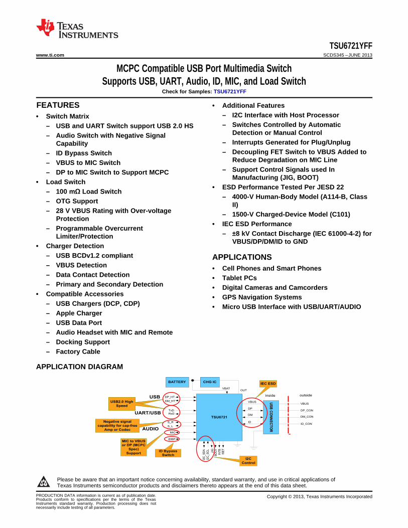
APPLICATION DIAGRAM
1
Please be aware that an important notice concerning availability, standard warranty, and use in critical applications ofTexas Instruments semiconductor products and disclaimers thereto appears at the end of this data sheet.
PRODUCTION DATA information is current as of publication date. Copyright © 2013, Texas Instruments IncorporatedProducts conform to specifications per the terms of the TexasInstruments standard warranty. Production processing does notnecessarily include testing of all parameters.
TSU6721YFFSCDS345 –JUNE 2013 www.ti.com
These devices have limited built-in ESD protection. The leads should be shorted together or the device placed in conductive foamduring storage or handling to prevent electrostatic damage to the MOS gates.
ORDERING INFORMATION
For package and ordering information, see the Package Option Addendum at the end of this document.
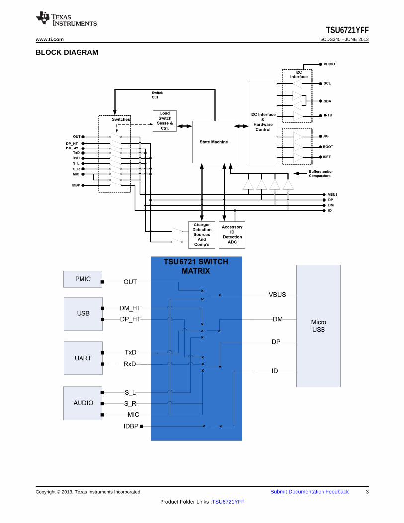
DESCRIPTIONTSU6721 is a high performance USB port multimedia switch featuring automatic switching and accessorydetection. The device connects a common USB port to pass audio, USB data, charging, On The Go (OTG) andfactory mode signals. The audio path has negative signal capability includes left (mono/stereo), right (stereo) aswell as microphone signals. Furthermore, TSU6721 is compatible with the MCPC specification.
TSU6721 features impedance detection which supports the detection of various accessories that are attachedthrough DP, DM and ID pins of the USB connector. The switch is controlled by automatic switching or manuallythrough I2C.
TSU6721 has an integrated low resistive Load Switch that is used to isolate the charger from the externalconnector. OverVoltage Protection and programmable OverCurrent Limiter/Protection are additional featuresincluded to the Load Switch.
The charger detection satisfies USB charger specification v1.2. In addition to DCP, CDP and SDP, the devicealso detects Apple Chargers.
Power for this device is supplied through VBAT of the system or through VBUS when attached. TSU6721supports factory mode testing when a USB/UART JIG cable is used in development and manufacturing.
2 Submit Documentation Feedback Copyright © 2013, Texas Instruments Incorporated
Product Folder Links :TSU6721YFF
TSU6721 SWITCH
MATRIX
UART
USBDP_HT
TxD
RxD
DM_HT
VBUS
DM
DP
ID
AUDIO S_R
S_L
MIC
PMIC OUT
Micro
USB
IDBP
Charger
DetectionSources
And
Comp’s
Accessory
IDDetection
ADC
I2C Interface
&Hardware
Control
Load
SwitchSense &
Ctrl.
VBUS
DP
DM
ID
Buffers and/or
Comparators
JIG
INTB
SDA
SCL
VDDIO
ISET
BOOT
I2CInterface
Switches
MIC
S_R
S_L
RxD
TxD
DM_HT
DP_HT
OUT
State Machine
Switch
Ctrl
IDBP
TSU6721YFFwww.ti.com SCDS345 –JUNE 2013
BLOCK DIAGRAM
Copyright © 2013, Texas Instruments Incorporated Submit Documentation Feedback 3
Product Folder Links :TSU6721YFF

INTB VDDIO ISET OUT VBUS
DP_
HTSDA S_L MIC DM
DM_
HTSCL NC S_R DP
VBAT IDBP GND GND ID
RxD TxD BOOT JIG GND
A
B
C
D
E
1 2 3 4 5
VBUS OUT ISET VDDIO INTB
DM MIC S_L SDADP_
HT
DP S_R NC SCLDM_
HT
ID GND GND IDBP VBAT
GND JIG BOOT TxD RxD
A
B
C
D
E
5 4 3 2 1
TSU6721YFFSCDS345 –JUNE 2013 www.ti.com
PIN OUT
TOP VIEW BOTTOM VIEW
PIN FUNCTIONSBALL NO. PIN NAME TYPE DESCRIPTION
D1 VBAT – 3.0 – 4.4V Battery supply voltage
A2 VDDIO – 1.8 ~ 3.3V Logic Supply
A5 VBUS I USB connector VBUS
A4 OUT O Phone charger output
E5, D3, D4 GND – Ground
B1 DP_HT I/O USB data plus
C1 DM_HT I/O USB data minus
D2 IDBP I/O USB ID data
E1 RxD I/O UART receive data
E2 TxD I/O UART transmit data
C3 NC – Not connected internally
B4 MIC I/O Microphone signal
C4 S_R I/O Stereo headset right sound
B3 S_L I/O Mono or stereo headset left sound
C2 SCL I I2C clock
B2 SDA I/O I2C data
C5 DP I/O Common USB connector plus I/O port
B5 DM I/O Common USB connector minus I/O port
D5 ID I/O Common USB connector ID I/O port
A1 INTB O Interrupt signal when peripheral is plugged/unplugged. Push-pull output
A3 ISET O High current charger detected. Open-drain output
E4 JIG O GPIO factory output. Open-drain output
E3 BOOT O GPIO factory output. Push-pull output
4 Submit Documentation Feedback Copyright © 2013, Texas Instruments Incorporated
Product Folder Links :TSU6721YFF
TSU6721YFFwww.ti.com SCDS345 –JUNE 2013
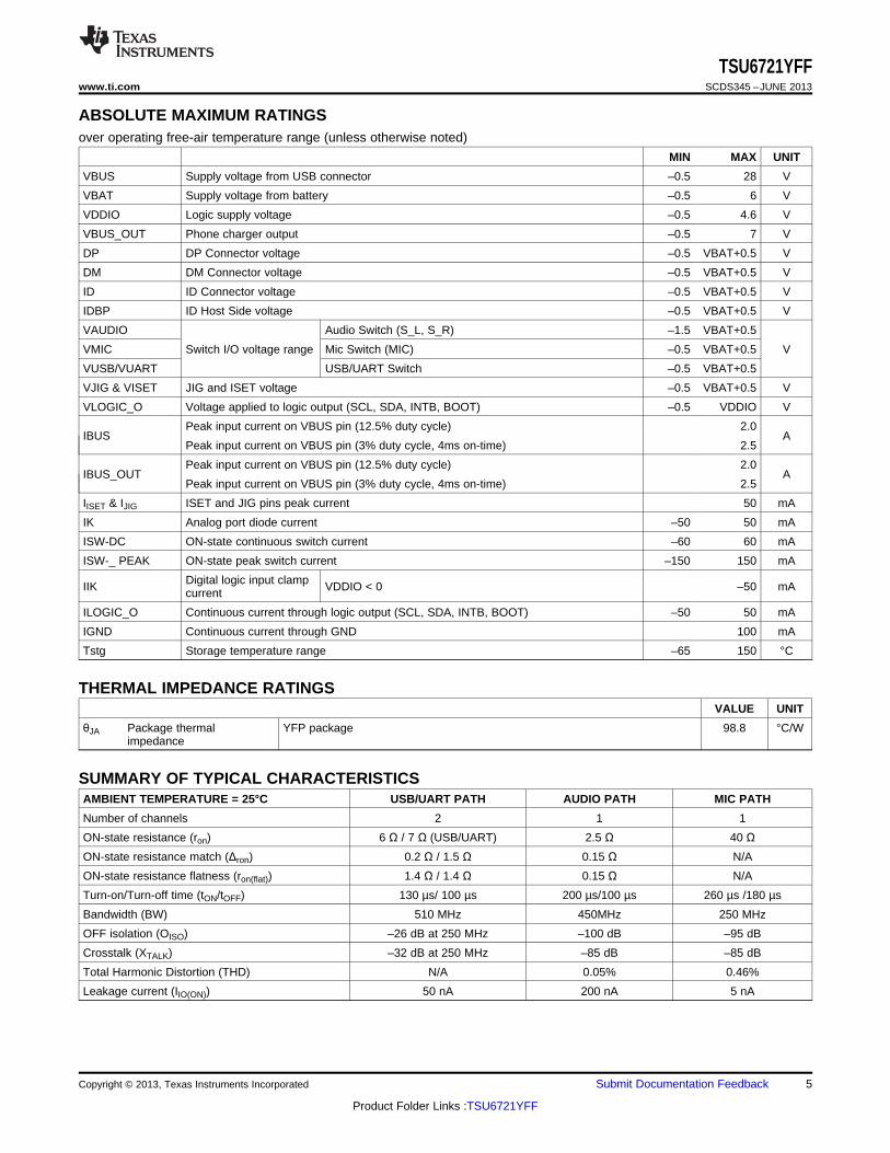
ABSOLUTE MAXIMUM RATINGSover operating free-air temperature range (unless otherwise noted)
MIN MAX UNIT
VBUS Supply voltage from USB connector –0.5 28 V
VBAT Supply voltage from battery –0.5 6 V
VDDIO Logic supply voltage –0.5 4.6 V
VBUS_OUT Phone charger output –0.5 7 V
DP DP Connector voltage –0.5 VBAT+0.5 V
DM DM Connector voltage –0.5 VBAT+0.5 V
ID ID Connector voltage –0.5 VBAT+0.5 V
IDBP ID Host Side voltage –0.5 VBAT+0.5 V
VAUDIO Audio Switch (S_L, S_R) –1.5 VBAT+0.5
VMIC Switch I/O voltage range Mic Switch (MIC) –0.5 VBAT+0.5 V
VUSB/VUART USB/UART Switch –0.5 VBAT+0.5
VJIG & VISET JIG and ISET voltage –0.5 VBAT+0.5 V
VLOGIC_O Voltage applied to logic output (SCL, SDA, INTB, BOOT) –0.5 VDDIO V
Peak input current on VBUS pin (12.5% duty cycle) 2.0IBUS A
Peak input current on VBUS pin (3% duty cycle, 4ms on-time) 2.5
Peak input current on VBUS pin (12.5% duty cycle) 2.0IBUS_OUT A
Peak input current on VBUS pin (3% duty cycle, 4ms on-time) 2.5
IISET & IJIG ISET and JIG pins peak current 50 mA
IK Analog port diode current –50 50 mA
ISW-DC ON-state continuous switch current –60 60 mA
ISW-_ PEAK ON-state peak switch current –150 150 mA
Digital logic input clampIIK VDDIO < 0 –50 mAcurrent
ILOGIC_O Continuous current through logic output (SCL, SDA, INTB, BOOT) –50 50 mA
IGND Continuous current through GND 100 mA
Tstg Storage temperature range –65 150 °C
THERMAL IMPEDANCE RATINGSVALUE UNIT
θJA Package thermal YFP package 98.8 °C/Wimpedance
SUMMARY OF TYPICAL CHARACTERISTICSAMBIENT TEMPERATURE = 25°C USB/UART PATH AUDIO PATH MIC PATH
Number of channels 2 1 1
ON-state resistance (ron) 6 Ω / 7 Ω (USB/UART) 2.5 Ω 40 ΩON-state resistance match (Δron) 0.2 Ω / 1.5 Ω 0.15 Ω N/A
ON-state resistance flatness (ron(flat)) 1.4 Ω / 1.4 Ω 0.15 Ω N/A
Turn-on/Turn-off time (tON/tOFF) 130 µs/ 100 µs 200 µs/100 µs 260 µs /180 µs
Bandwidth (BW) 510 MHz 450MHz 250 MHz
OFF isolation (OISO) –26 dB at 250 MHz –100 dB –95 dB
Crosstalk (XTALK) –32 dB at 250 MHz –85 dB –85 dB
Total Harmonic Distortion (THD) N/A 0.05% 0.46%
Leakage current (IIO(ON)) 50 nA 200 nA 5 nA
Copyright © 2013, Texas Instruments Incorporated Submit Documentation Feedback 5
Product Folder Links :TSU6721YFF

TSU6721YFFSCDS345 –JUNE 2013 www.ti.com
RECOMMENDED OPERATING CONDITIONSover operating free-air temperature range (unless otherwise noted)
PARAMETER DESCRIPTION MIN MAX UNITS
VBUS VBUS voltage 4.0 6.5 V
VBAT VBAT voltage 3.0 4.4 V
VDDIO VDDIO voltage 1.65 3.6 V
ID_Cap ID capacitance 3 nF
USB_I/O USB path signal range 0 3.6 V
UART_I/O UART path signal range 0 2.7 V
Audio_I/O Audio path signal range –1.5 1.5 V
MIC_I/O MIC path signal range 0 2.3 V
Temperature Operating Temperature –40 85 °C
ELECTRICAL SPECIFICATIONS
DIGITAL SIGNALS – I2C INTERFACE (SCL and SDA)TA = –40°C to 85°C, Typical values are at TA = 25°C (unless otherwise noted)
PARAMETER TEST CONDITIONS MIN MAX UNIT
VDDIO Logic and I/O supply voltage 1.65 3.6 V
VIH High-level input voltage VDDIO × 0.7 VDDIO V
VIL Low-level input voltage 0 VDDIO × 0.3 V
VOH SDA High-level output voltage IOH = –3 mA VDDIO × 0.7 V
VOL SDA Low-level output voltage IOL = 3 mA 0 0.4 V
fSCL SCL frequency 400 kHz
JIG AND ISET FAST-MODE CHARGER OUTPUT (OPEN-DRAIN OUTPUT)TA = –40°C to 85°C, Typical values are at TA = 25°C (unless otherwise noted)
PARAMETER TEST CONDITIONS MIN MAX UNIT
VOL_JIG Low-level output voltage IOL = 10 mA, VBAT = 3.0 V 0 0.5 V
VOL_ISET Low-level output voltage IOL = 10 mA, VBAT = 3.0 V 0 0.7 V
INTB AND BOOT (PUSH-PULL OUTPUT)TA = –40°C to 85°C, Typical values are at TA = 25°C (unless otherwise noted)
PARAMETER TEST CONDITIONS MIN MAX UNIT
VOH High-level output voltage IOH = –4 mA , VDDIO = 1.65 V 1.16 VDDIO V
VOL Low-level output voltage IOL = 4 mA , VDDIO = 1.65 V 0 0.33 V
TOTAL SWITCH CURRENT CONSUMPTIONTA = –40°C to 85°C, Typical values are at TA = 25°C (unless otherwise noted)
PARAMETER TEST CONDITIONS MIN TYP MAX UNIT
IBAT(Standby) VBAT Standby Current Consumption VBUS = 0 V, Idle state 36 50 µA
IBAT(Operating) VBAT Operating Current Consumption VBUS = 0 V, USB switches ON 60 80 µA
IVBUS VBUS Operating Current Consumption No load on OUT pin, VBUS = 5 V 135 155 µA
VBUS CAP SWITCH CHARACTERISTICSTA = –40°C to 85°C, Typical values are at TA = 25°C (unless otherwise noted)
PARAMETER TEST CONDITIONS MIN TYP MAX UNIT
RDS-VBUSCAP VBUS CAP switch resistance VBUS = 5 V, IOUT = –20 mA 90 Ω
6 Submit Documentation Feedback Copyright © 2013, Texas Instruments Incorporated
Product Folder Links :TSU6721YFF

TSU6721YFFwww.ti.com SCDS345 –JUNE 2013
VOLTAGE PROTECTIONTA = –40°C to 85°C, Typical values are at TA = 25°C (unless otherwise noted)
PARAMETER TEST CONDITIONS MIN TYP MAX UNIT
VVBUS_UVLO VBUS under voltage+ Voltage is Rising, device power-up 3.0 3.25 3.6 V
VBUS under voltage– Voltage is Falling, device reset 2.7 3 3.3
VVBUS_VALID VBUS interrupt threshold Voltage is Rising 3.6 V
VVBAT_UVLO VBAT under voltage+ Voltage is Rising, device power-up 2.5 2.8 3.1 V
VBAT under voltage– Voltage is Falling, device reset 2.3 2.6 2.9
LOAD SWITCH CHARACTERISTICSTA = –40°C to 85°C, Typical values are at TA = 25°C (unless otherwise noted)
PARAMETER TEST CONDITIONS MIN TYP MAX UNIT
RDS- VBUS switch resistance VBUS = 5 V, IOUT = 100 mA 90 150 mΩVBUSSWITCH
tONa Turn-ON time automatic mode RL = 36 Ω, CL = 400 pF, Vbus rising > 3.6V 175 ms
tOFFa Turn-OFF time automatic mode RL = 36 Ω, CL = 400 pF, Vbus falling < 3.6V 2.5 ms
RL = 36 Ω, CL = 400 pF, From receipt of I2C ACKtONm Turn-ON time manual mode 230 µsbit
RL = 36 Ω, CL = 400 pF, From receipt of I2C ACKtOFFm Turn-OFF time manual mode 180 µsbit
I2C reg0x22h, Bit [2:0] = 000 0.8 1.0 1.2
I2C reg0x22h, Bit [2:0] = 001 (default) 1.3 1.5 1.7Programmable overcurrentIOCP VBUS = 5.5V Aprotection I2C reg0x22h, Bit [2:0] = 010 2.0
I2C reg0x22h, Bit [2:0] = 011 2.0
I2C reg0x21h, Bit [7:5] = 000 1.25 1.5 1.75
I2C reg0x21h, Bit [7:5] = 001 (default) 1.67 2.0 2.33IOCL Programmable overcurrent limiter VBUS = 5.5V A
I2C reg0x21h, Bit [7:5] = 010 2.5
I2C reg0x21h, Bit [7:5] = 011 2.5
VBUS OVERVOLTAGE PROTECTION (OVP)
VBUS Input overvoltage protection VBUS increasing from 6 V to 8 V 6.8 7 7.2 VthresholdVOVP
VBUSOVP delay Delay from VBUS > VOVP to Load switch OFF 200 µs
tOFF(OVP)
VBUSHysteresis on OVP VBUS decreasing from 8 V to 6 V 140 mV
VHYS-OVP
VBUS Recovery time from input Delay from VBUS < VOVP-VHYS, to Load switch ON 9 msovervoltage conditiontON(OVP)
OTPOTP Rising Turn Off Temperature rising until load switch shut off 130 °C
rOTP
OTP Temperature falling after OTP shutoff until switchOTP Falling Turn On 120 °Cturn onfOTP
Copyright © 2013, Texas Instruments Incorporated Submit Documentation Feedback 7
Product Folder Links :TSU6721YFF

TSU6721YFFSCDS345 –JUNE 2013 www.ti.com
AUDIO SWITCH ELECTRICAL CHARACTERISTICS (1) (2)
VBAT = 3.0 V to 4.4 V, VDDIO = 2.8 V, TA = –40°C to 85°C, Typical values are at TA = 25°C (unless otherwise noted)
PARAMETER TEST CONDITIONS MIN TYP MAX UNIT
ANALOG SWITCH
VAUDIO Analog signal range –1.5 3 V
rON ON-state resistance S_L or VI = ±0.8 V, IO = –20 mA, VBAT = 3.0 V 2.5 5 ΩS_R , DM orΔrON ON-state resistance match VI = 0.8 V, II = –20 mA, VBAT = 3.0 V 0.15 0.5 ΩDPbetween channels
rON(flat) ON-state resistance VI = ±0.8 V, IO = –20 mA, VBAT = 3.0 V 0.15 0.5 Ωflatness
(VI = -0.8 V, VO = 0.8 V) or (VI = 0.8 V,IIO(OFF) VI or VO OFF leakage current 200 500 nA
VO = –0.8 V), VBAT = 4.4 V, Switch OFF
IIO(ON) VO ON leakage current VI = OPEN, VO = –0.8 V or 0.8 V, VBAT = 4.4 V, 10 300 nASwitch ON
DYNAMIC
tON Turn-ON time From 200 µsreceipt of VI or VO = VBAT, RL = 100 Ω, CL = 35 pFtOFF Turn-OFF time 100I2C ACK bit
CI(OFF) VI OFF capacitance 5.5 pFDC bias = 0 V or 1.6 V f = 10 MHz, Switch OFF
CO(OFF) VO OFF capacitance 10 pF
CI(ON), CO(ON) VI, VO ON capacitance DC bias = 0 V or 1.6 V f = 10 MHz, Switch ON 13 pF
BW Bandwidth RL = 50 Ω, Switch ON 450 MHz
OISO OFF Isolation f = 20 kHz, RL = 50 Ω, Switch OFF –100 dB
XTALK Crosstalk f = 20 kHz, RL = 50 Ω –85 dB
THD Total harmonic distortion RL = 16 Ω, CL = 20 pF, f = 20 Hz–20 kHz , 0.05 %1.6 Vpp output
RL = 16 Ω, CL = 20 pF, f = 20 Hz–20 kHz , 0.1 %3 Vpp output
(1) VI is equal to the asserted voltage on S_R and S_L pins. VO is equal to the asserted voltage on DP and DM pins. II is equal to thecurrent on the S_R and S_L pins. IO is equal to the current on the DP and DMpins
(2) Audio Switch is intended for signals to be asserted on S_R/S_L pins and pass to DM/DP
8 Submit Documentation Feedback Copyright © 2013, Texas Instruments Incorporated
Product Folder Links :TSU6721YFF

TSU6721YFFwww.ti.com SCDS345 –JUNE 2013
MIC SWITCH ELECTRICAL CHARACTERISTICS (1)
VBAT = 3.0 V to 4.4 V, VDDIO = 2.8 V, TA = –40°C to 85°C, Typical values are at TA = 25°C (unless otherwise noted)
PARAMETER TEST CONDITIONS MIN TYP MAX UNIT
ANALOG SWITCH
VMICIO Analog signal range 0 VBAT V
rON ON-state resistance MIC, VBUS VI = 2.3 V, IO = –20 mA, VBAT = 3.0 V 40 52 ΩMIC, DP VI = 2.3 V, II = –5 mA, VBAT = 3.0 V 15 25 Ω
IIO(OFF) VI or VO OFF leakage current VI = 0.3 V, VO = 2.3 V or (VI = 2.3 V, VO = 0.3 5 500 nAV),VBAT = 4.4 V, Switch OFF
DYNAMIC
tON Turn-ON time From receipt of VI or VO = VBAT, RL = 100 Ω, CL = 35 pF 260 µsI2C ACK bittOFF Turn-OFF time 180
CI(OFF) VI OFF capacitance DC bias = 0 V or 3.6 V, f = 10 MHz, Switch OFF 130 pF
CO(OFF) VO OFF capacitance 10.5 pF
CI(ON), CO(ON) VI, VO ON capacitance DC bias = 0 V or 3.6 V f = 10 MHz, Switch ON 140 pF
BW Bandwidth, MIC to VBUS RL = 50 Ω, Switch ON 40 MHz
Bandwidth, MIC to DP RL = 50 Ω, Switch ON 250
OISO OFF Isolation f = 20 kHz, RL = 50 Ω, Switch OFF –95 dB
XTALK Crosstalk f = 20 kHz, RL = 50 Ω, to audio output –85 dB
THD Total harmonic distortion RL = 600 Ω, CL = 20 pF, f = 20 Hz–20 kHz , 0.05 0.65 %Vin = 0.1 Vpp centered at VBAT/2
(1) VI is equal to the asserted voltage on VBUS/DP pin. VO is equal to the asserted voltage on MIC pin. II is equal to the current on theVBUS/DP pin. IO is equal to the current on the MIC pin.
Copyright © 2013, Texas Instruments Incorporated Submit Documentation Feedback 9
Product Folder Links :TSU6721YFF

TSU6721YFFSCDS345 –JUNE 2013 www.ti.com
USB & UART SWITCH ELECTRICAL CHARACTERISTICSVBAT = 3 V to 4.4 V, VDDIO = 2.8 V, TA = –40°C to 85°C, Typical values are at TA = 25°C (unless otherwise noted)
PARAMETER TEST CONDITIONS MIN TYP MAX UNIT
ANALOG SWITCH
VUSBIO Analog signal range 0 3.6 V
VUARTIO Analog signal range 0 2.7
rON ON-state resistance DM_HT,DM VI = 0 V to 3.6 V, IO = –20 mA, VBAT = 3.0 6 11 ΩDP_HT,DP V
TxD, DM VI = 0 V to 3.6 V, IO = –20 mA, VBAT = 3.0 7 14.3RxD, DP V
rON ON-state resistance ID, IDBP VI = 0 V to 3.6 V, IO = –20 mA, VBAT = 3.0 30 ΩV
ΔrON ON-state resistance match DM_HT,DM VI = 0.4 V, IO = –20 mA, VBAT = 3.0 V 0.2 1 Ωbetween channels DP_HT,DP
TxD, DM VI = 0.4 V, IO = –20 mA, VBAT = 3.0 V 1.5 3RxD, DP
rON(flat) ON-state resistance DM_HT, DP_HT, VI = 0 V to 3.6 V, IO = –20 mA, 1.4 3.2 Ωflatness TxD, RxD, DM, DP VBAT = 3.0 V
IIO(OFF) VI or VO OFF leakage DM_HT, DP_HT, VI = 0.3 V, VO = 2.7 V or VI = 2.7 V, 45 200 nAcurrent TxD, RxD, DM, DP VO = 0.3 V, VBAT = 4.4 V, Switch OFF
IIO(ON) VO ON leakage current DM_HT, DP_HT, VI = OPEN, VO = 0.3 V or 2.7 V, 50 200 nATxD, RxD, DM, DP VBAT = 4.4 V, Switch ON
DYNAMIC
tON Turn-ON time From receipt of I2C VI or VO = VBAT, RL = 100 Ω, CL = 35 pF 130 µsACK bittOFF Turn-OFF time 100
CI(OFF) VI OFF capacitance DC bias = 0 V or 1.6 V, f = 10 MHz, 4 pFSwitch OFFCO(OFF) VO OFF capacitance 7 pF
CI(ON), CO(ON) VI, VO ON capacitance DC bias = 0 V or 3.6 V f = 10 MHz, 9 pFSwitch ON
BW Bandwidth RL = 50 Ω, Switch ON 510 MHz
OISO OFF Isolation f = 240 kHz, RL = 50 Ω, Switch OFF –26 dB
XTALK Crosstalk f = 240 kHz, RL = 50 Ω –32 dB
10 Submit Documentation Feedback Copyright © 2013, Texas Instruments Incorporated
Product Folder Links :TSU6721YFF

TSU6721YFFwww.ti.com SCDS345 –JUNE 2013
GENERAL OPERATION
The TSU6721 is a multimedia switch that connects a common USB connector to USB, UART or audio signals.The device also has a MIC switch that connects to either VBUS or DP. It has an integrated load switch to supportcharging. The load switch has OverVoltage Protection as well as OverCurrent Limiting Protection. In addition, theTSU6721 also has an ID bypass switch to transmit ID signal from the connector to the host. It has an internalFET switch that disconnects the coupling capacitor connected to the VBUS line.
Standby Mode
Standby mode is the default mode upon power up and occurs when no accessory has been detected. During thismode, the VBUS and ID lines are continually monitored through comparators to determine when an accessory isinserted. Power consumption is minimal during standby mode.
Load Switch
The integrated load switch provides both overvoltage/undervoltage and overcurrent limiting protection:
Overvoltage Protection
When the input voltage rises above VOVP, the internal load switch is turned off. The response is very rapid, withthe FET turning off in less than 1µs tOFF(OVP). The OVP_EN interrupt bit is set high when an overvoltagecondition is detected. When the input voltage returns below VOVP-VHYS_OVP and remains above VUVLO, theVBUS switch is turned on again after a deglitch time of tON(OVP). This deglitch time ensures that the inputsupply has stabilized before turning the switch on. When the OVP condition is cleared, the OVP_OCP_DISinterrupt bit is set high.
Undervoltage Protection
When VBUS is not present and VBAT is less than 2.5V, VBAT and VBUS voltages are below the undervoltagethreshold and TSU6721 is powered off.
Overcurrent Limiting Protection
The TSU6721 also provides overcurrent limiting protection. When current increases beyond the IOCP threshold, atime-out delay is initiated. After the delay has expired, and the current is still greater than IOCP, then load switch isdisabled. The maximum current that flows through the load switch is controlled by the IOCL limit. This featureprovides control on the VBUS charging current and minimizes the chance of internal circuitry damage caused byovercurrent event. The overcurrent level can be programmed through I2C.
Power Supervisor
TSU6721 uses VBAT as the primary supply voltage. VBUS is the secondary supply. VDDIO is used for I2Ccommunication.
Table 1. Supply Voltage States
VBAT VBUS VDDIO DETECTION LOAD SWITCH I2C COMMENTS
Yes No No Enabled Not Enabled Not Enabled VBAT is supply
Yes Yes No Enabled Enabled Not enabled VBAT is supply. LOAD SWITCH controlled byVBUS
Yes No Yes Enabled Not Enabled Enabled VBAT is supply
Yes Yes Yes Enabled Enabled Enabled VBAT is supply. LOAD SWITCH controlled byVBUS
No Yes No Enabled Enabled Not Enabled VBUS is supply. LOAD SWITCH controlled byVBUS
No Yes Yes Not valid
No No Yes Not valid
No No No Power Down Reset
Copyright © 2013, Texas Instruments Incorporated Submit Documentation Feedback 11
Product Folder Links :TSU6721YFF
RID
VCC
ID
TSU6721
GND
D+
D-
VBUS
ISRC
VREF
CID,MAX
(1)
TSU6721YFFSCDS345 –JUNE 2013 www.ti.com
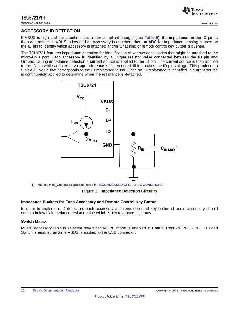
ACCESSORY ID DETECTION
If VBUS is high and the attachment is a non-compliant charger (see Table 5), the impedance on the ID pin isthen determined. If VBUS is low and an accessory is attached, then an ADC for impedance sensing is used onthe ID pin to identify which accessory is attached and/or what kind of remote control key button is pushed.
The TSU6721 features impedance detection for identification of various accessories that might be attached to themicro-USB port. Each accessory is identified by a unique resistor value connected between the ID pin andGround. During impedance detection a current source is applied to the ID pin. The current source is then appliedto the ID pin while an internal voltage reference is incremented till it matches the ID pin voltage. This produces a5-bit ADC value that corresponds to the ID resistance found. Once an ID resistance is identified, a current sourceis continuously applied to determine when the resistance is detached.
(1) Maximum ID_Cap capacitance as noted in RECOMMENDED OPERATING CONDITIONS
Figure 1. Impedance Detection Circuitry
Impedance Buckets for Each Accessory and Remote Control Key Button
In order to implement ID detection, each accessory and remote control key button of audio accessory shouldcontain below ID impedance resistor value which is 1% tolerance accuracy.
Switch Matrix
MCPC accessory table is selected only when MCPC mode is enabled in Control Reg02h. VBUS to OUT LoadSwitch is enabled anytime VBUS is applied to the USB connector.
12 Submit Documentation Feedback Copyright © 2013, Texas Instruments Incorporated
Product Folder Links :TSU6721YFF
TSU6721YFFwww.ti.com SCDS345 –JUNE 2013
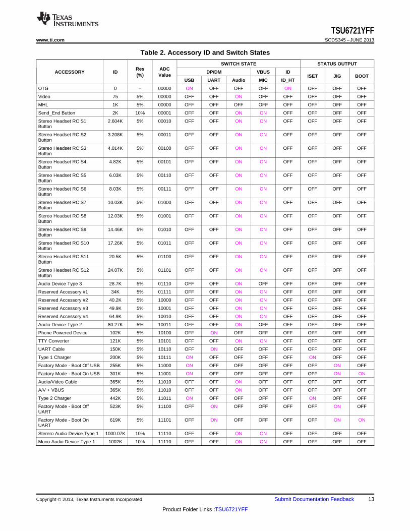
Table 2. Accessory ID and Switch States
SWITCH STATE STATUS OUTPUTRes ADC
ACCESSORY ID DP/DM VBUS ID(%) Value ISET JIG BOOT
USB UART Audio MIC ID_HT
OTG 0 – 00000 ON OFF OFF OFF ON OFF OFF OFF
Video 75 5% 00000 OFF OFF ON OFF OFF OFF OFF OFF
MHL 1K 5% 00000 OFF OFF OFF OFF OFF OFF OFF OFF
Send_End Button 2K 10% 00001 OFF OFF ON ON OFF OFF OFF OFF
Stereo Headset RC S1 2.604K 5% 00010 OFF OFF ON ON OFF OFF OFF OFFButton
Stereo Headset RC S2 3.208K 5% 00011 OFF OFF ON ON OFF OFF OFF OFFButton
Stereo Headset RC S3 4.014K 5% 00100 OFF OFF ON ON OFF OFF OFF OFFButton
Stereo Headset RC S4 4.82K 5% 00101 OFF OFF ON ON OFF OFF OFF OFFButton
Stereo Headset RC S5 6.03K 5% 00110 OFF OFF ON ON OFF OFF OFF OFFButton
Stereo Headset RC S6 8.03K 5% 00111 OFF OFF ON ON OFF OFF OFF OFFButton
Stereo Headset RC S7 10.03K 5% 01000 OFF OFF ON ON OFF OFF OFF OFFButton
Stereo Headset RC S8 12.03K 5% 01001 OFF OFF ON ON OFF OFF OFF OFFButton
Stereo Headset RC S9 14.46K 5% 01010 OFF OFF ON ON OFF OFF OFF OFFButton
Stereo Headset RC S10 17.26K 5% 01011 OFF OFF ON ON OFF OFF OFF OFFButton
Stereo Headset RC S11 20.5K 5% 01100 OFF OFF ON ON OFF OFF OFF OFFButton
Stereo Headset RC S12 24.07K 5% 01101 OFF OFF ON ON OFF OFF OFF OFFButton
Audio Device Type 3 28.7K 5% 01110 OFF OFF ON OFF OFF OFF OFF OFF
Reserved Accessory #1 34K 5% 01111 OFF OFF ON ON OFF OFF OFF OFF
Reserved Accessory #2 40.2K 5% 10000 OFF OFF ON ON OFF OFF OFF OFF
Reserved Accessory #3 49.9K 5% 10001 OFF OFF ON ON OFF OFF OFF OFF
Reserved Accessory #4 64.9K 5% 10010 OFF OFF ON ON OFF OFF OFF OFF
Audio Device Type 2 80.27K 5% 10011 OFF OFF ON OFF OFF OFF OFF OFF
Phone Powered Device 102K 5% 10100 OFF ON OFF OFF OFF OFF OFF OFF
TTY Converter 121K 5% 10101 OFF OFF ON ON OFF OFF OFF OFF
UART Cable 150K 5% 10110 OFF ON OFF OFF OFF OFF OFF OFF
Type 1 Charger 200K 5% 10111 ON OFF OFF OFF OFF ON OFF OFF
Factory Mode - Boot Off USB 255K 5% 11000 ON OFF OFF OFF OFF OFF ON OFF
Factory Mode - Boot On USB 301K 5% 11001 ON OFF OFF OFF OFF OFF ON ON
Audio/Video Cable 365K 5% 11010 OFF OFF ON OFF OFF OFF OFF OFF
A/V + VBUS 365K 5% 11010 OFF OFF ON OFF OFF OFF OFF OFF
Type 2 Charger 442K 5% 11011 ON OFF OFF OFF OFF ON OFF OFF
Factory Mode - Boot Off 523K 5% 11100 OFF ON OFF OFF OFF OFF ON OFFUART
Factory Mode - Boot On 619K 5% 11101 OFF ON OFF OFF OFF OFF ON ONUART
Sterero Audio Device Type 1 1000.07K 10% 11110 OFF OFF ON ON OFF OFF OFF OFF
Mono Audio Device Type 1 1002K 10% 11110 OFF OFF ON ON OFF OFF OFF OFF
Copyright © 2013, Texas Instruments Incorporated Submit Documentation Feedback 13
Product Folder Links :TSU6721YFF

TSU6721YFFSCDS345 –JUNE 2013 www.ti.com
Table 3. Accessory ID and Switch States MCPC Mode
SWITCH STATE STATUS OUTPUT
ADC DP/DM VBUS IDACCESSORY ID RES (%)VALUE ISET JIG BOOTAUDIUSB UART MIC ID_HTO
10000Send_End_SW 47K 5% OFF OFF ON ON OFF OFF OFF OFF
10001
10000Send_End_SW with VBUS 47K 5% OFF OFF ON OFF OFF OFF OFF OFF
10001
10110Maintanence 180K 5% OFF OFF OFF OFF OFF OFF OFF OFF
10111
11000 ON ON OFF OFF OFF OFFMode 1 Stereo 47K + 240K 5% OFF OFF
11001
11000 ON OFF OFF OFF OFF OFFMode 1 Stereo with VBUS 47K + 240K 5% OFF OFF
11001
11010 OFF OFF OFF OFF OFF OFFReserved 390K 5% OFF OFF
11011
11100 OFF OFF OFF OFF OFFMode 3 Monaural 47K + 510K 5% DM to S_L; DP to MIC
11101
11100 OFF OFF OFF OFF OFFMode 3 Monaural with VBUS 47K + 510K 5% DM to S_L; DP to MIC
11101
Mode 2 Monaural 47K + 750K 5% 11110 DM to S_L; DP OPEN ON OFF OFF OFF OFF
Mode 2 Monaural with VBUS 47K + 750K 5% 11110 DM to S_L; DP OPEN OFF OFF OFF OFF OFF
14 Submit Documentation Feedback Copyright © 2013, Texas Instruments Incorporated
Product Folder Links :TSU6721YFF

TSU6721YFFwww.ti.com SCDS345 –JUNE 2013
CHARGER DETECTION
Table 4. Chargers Detected and Switch States
SWITCH STATE STATUS OUTPUTADCACCESSORY ID RES (%) DP/DM VBUS IDVALUE ISET JIG BOOT
USB UART AUDIO MIC ID_HT
No ID – – 11111 OFF OFF OFF OFF OFF OFF OFF OFF
Apple Charger – – 11111 OFF OFF OFF OFF OFF OFF OFF OFF
Non-standard Charger – – 11111 OFF OFF OFF OFF OFF OFF OFF OFF
USB Standard Downstream – – 11111 ON OFF OFF OFF ON OFF OFF OFFPort
USB Charging Downstream – – 11111 ON OFF OFF OFF ON ON OFF OFFPort
Dedicated Charging Port – – 11111 ON OFF OFF OFF ON ON OFF OFF
Table 5 lists the configurations of the DP_CON (D+) and DM_CON (D-) that are internal to the various devicetypes.
Table 5. Charger Detection Table
DEVICE TYPE VBUS DP_CON (D+) DM_CON (D–)
Standard Downstream Port >4 V Pull-down R 15k to GND Pull-down R 15k
Charging Downstream Port >4 V Pull-down R 15k to GND VDM_SRC =0.6V
Dedicated Charging Port >4 V Short to D– Short to D+
Apple Charger >4 V 2.0 < VDP < 2.8 2.0 < VDM < 2.8
U200 >4 V VDP = 1.34 VDM = 1.34
Non-compliant USB Charger Any >4 V Open OpenDevice
Power-On Reset
When power (from 0 V) is applied to VBAT, an internal power-on reset holds the TSU6721 in a reset conditionuntil VBAT has reached VPOR. At that point, the reset condition is released, and the TSU6721 registers and I2Cstate machine initialize to their default states.
After the initial power-up phase, VBAT must be lowered to below 0.2 V and then back up to the operating voltage(VDDIO) for a power-reset cycle.
Software Reset
The TSU6721 has software a reset feature. Set the reset bit in the I2C register high to reset TSU6721. Afterresetting, INTB will keep low until INT_Mask bit of Control register (0x02) is cleared.
Copyright © 2013, Texas Instruments Incorporated Submit Documentation Feedback 15
Product Folder Links :TSU6721YFF
Key
INTB
Key PressInterrupt
Long KeyPress Interrupt
Long KeyRelease Interrupt
(A) (B) (C)
Long Key Press Timing
Key Press Timing
Key
INTB
Key PressInterrupt
Long KeyPress Interrupt
Long KeyRelease Interrupt
(A) (B) (C)
Key Press Timing
Long Key Press Timing
TSU6721YFFSCDS345 –JUNE 2013 www.ti.com
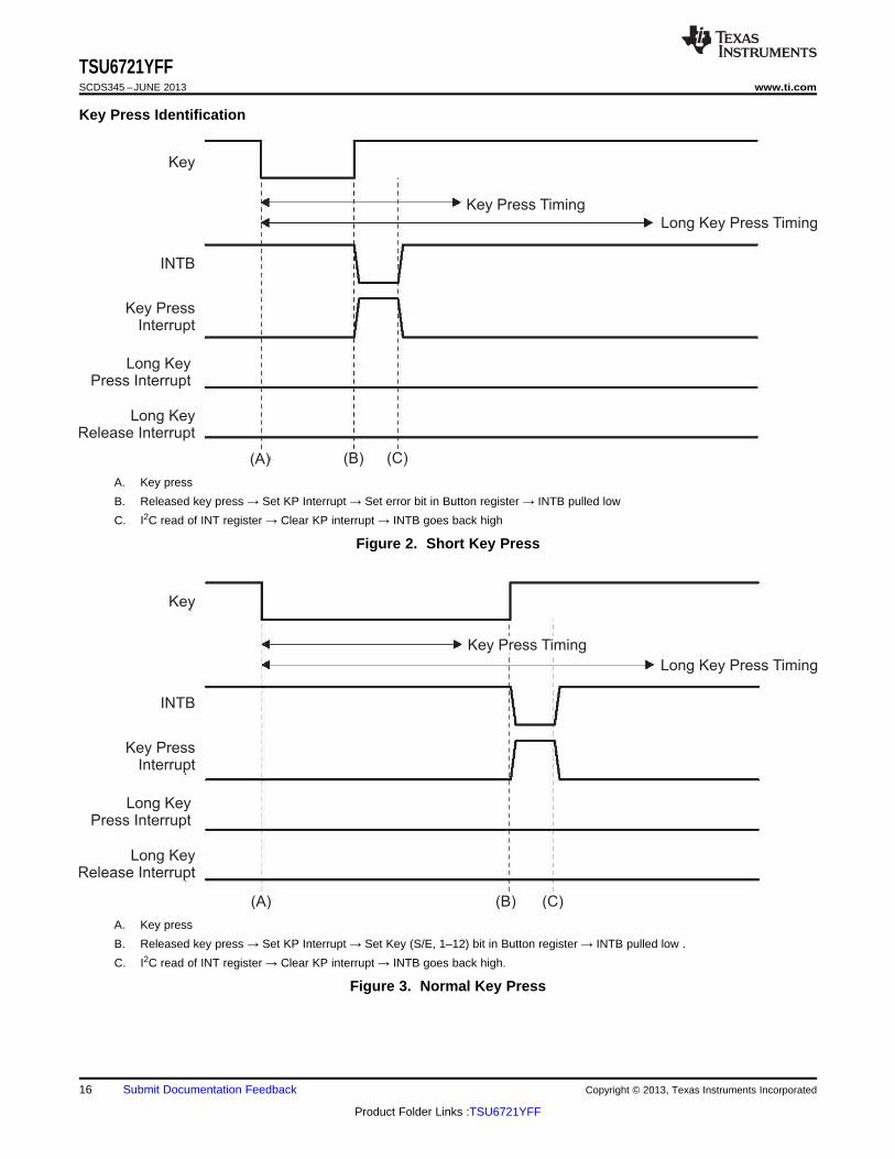
Key Press Identification
A. Key press
B. Released key press → Set KP Interrupt → Set error bit in Button register → INTB pulled low
C. I2C read of INT register → Clear KP interrupt → INTB goes back high
Figure 2. Short Key Press
A. Key press
B. Released key press → Set KP Interrupt → Set Key (S/E, 1–12) bit in Button register → INTB pulled low .
C. I2C read of INT register → Clear KP interrupt → INTB goes back high.
Figure 3. Normal Key Press
16 Submit Documentation Feedback Copyright © 2013, Texas Instruments Incorporated
Product Folder Links :TSU6721YFF

Key
INTB
Key PressInterrupt
Long KeyPress Interrupt
Long KeyRelease Interrupt
Long Key Press Timing
Key Press Timing
(A) (B) (C) (D) (E)
TSU6721YFFwww.ti.com SCDS345 –JUNE 2013
A. Key press
B. Long key press timing reached → Set LKP interrupt bit → Set Key (S/E, 1–12) bit in Button register → INTB pulledlow
C. I2C read of INT register → Clear LKP interrupt bit → INTB goes back high
D. Released key press → Set LKR Interrupt bit → INTB pulled low
E. I2C read of INT register → Clear LKR interrupt bit→ INTB goes back high
Figure 4. Long Key Press
Copyright © 2013, Texas Instruments Incorporated Submit Documentation Feedback 17
Product Folder Links :TSU6721YFF

Key
INTB
Key PressInterrupt
Long KeyPress Interrupt
Long KeyRelease Interrupt
Long Key Press Timing
Key Press Timing
(A) (B) (C) (D) (E)
TSU6721YFFSCDS345 –JUNE 2013 www.ti.com
A. Key press detected when accessory attached
B. Long key press timing reached → Set SK interrupt bit → Set Key (S/E, 1–12) bit in Button register → INTB pulled low
C. I2C read of INT register → Clear SK interrupt bit → INTB goes back high
D. Released key press detected when accessory ID resistor is 1 MΩ → Set SKR Interrupt bit → INTB pulled low
E. I2C read of INT register → Clear SKR interrupt bit → INTB goes back high
Figure 5. Stuck Key Press
Figure 6. Audio/Remote Controller Accessory
STANDARD I2C INTERFACE DETAILS
The bidirectional I2C bus consists of the serial clock (SCL) and serial data (SDA) lines. Both lines must beconnected to a positive supply via a pull-up resistor when connected to the output stages of a device. Datatransfer may be initiated only when the bus is not busy.
I2C communication with this device is initiated by the master sending a START condition, a high-to-low transitionon the SDA input/output while the SCL input is high (see Figure 7). After the start condition, the device addressbyte is sent, MSB first, including the data direction bit (R/W). This device does not respond to the general calladdress. After receiving the valid address byte, this device responds with an ACK, a low on the SDA input/outputduring the high of the ACK-related clock pulse.
18 Submit Documentation Feedback Copyright © 2013, Texas Instruments Incorporated
Product Folder Links :TSU6721YFF

S
1 2 8 9
NACK
ACK
Data Outputby Transmitter
Data Outputby Receiver
SCL FromMaster
StartCondition
Clock Pulse forAcknowledgment
SDA
SCL
Data Line Change
SDA
SCLS P
Start Condition Stop Condition
TSU6721YFFwww.ti.com SCDS345 –JUNE 2013
Figure 7. Definition of Start and Stop Conditions
The data byte follows the address ACK. The R/W bit is kept low for transfer from the master to the slave. Thedata byte is followed by an ACK sent from this device. Data are output only if complete bytes are received andacknowledged. The output data is valid at time (tpv) after the low-to-high transition of SCL, during the clock cyclefor the ACK.
On the I2C bus, only one data bit is transferred during each clock pulse. The data on the SDA line must remainstable during the high pulse of the clock period, as changes in the data line at this time are interpreted as controlcommands (START or STOP) (see Figure 8).
Figure 8. Bit Transfer
A Stop condition, a low-to-high transition on the SDA input/output while the SCL input is high, is sent by themaster (see Figure 7).
The number of data bytes transferred between the start and the stop conditions from transmitter to receiver is notlimited. Each byte of eight bits is followed by one ACK bit. The transmitter must release the SDA line before thereceiver can send an ACK bit.
A slave receiver that is addressed must generate an ACK after the reception of each byte. The device thatacknowledges has to pull down the SDA line during the ACK clock pulse so that the SDA line is stable low duringthe high pulse of the ACK-related clock period (see Figure 9). Setup and hold times must be taken into account.
Figure 9. Acknowledgment on I2C Bus
Copyright © 2013, Texas Instruments Incorporated Submit Documentation Feedback 19
Product Folder Links :TSU6721YFF

SDA ST 0 1 0 0 1 0 1 0 A 0 0 0 0 0 0 1 1 A RS 0 1 0 0 1 0 1 1 A D7 D6 D5 D4 D3 D2 D1 D0
Start
Slave Address
W/R
ACK From Slave
Sub Address
ACKFromSlaveAuto-Inc.
Slave Address
W/R
ACK From Slave
Re-Start
Date Byte
A A
ACK From Master
D7 D6 D5 D4 D3 D2 D1 D0
Date Byte
NAD7 D6 D5 D4 D3 D2 D1 D0
Date Byte
Data from Interrupt 1 Reg.
Data from Interrupt 1 Reg. Data from Interrupt 1 Reg.
ACK From Master No ACK From Master (Message Ends)
continued SP
Stop
Register Address
(Interrupt 1 Reg)
SDA ST 0 1 0 0 1 0 1 0 A 1 0 0 0 1 0 0 0 A D7 D6 D5 D4 D3 D2 D1 D0 A D7 D6 D5 D4 D3 D2 D1 D0 A
Start
Slave Address
W/R
ACK From Slave
Sub Address
ACKFromSlaveAuto-Inc.
ACKFromSlave
ACKFromSlave
Data to Timing Set 1
Register
Data to Timing Set 2
Register
Date Byte Date Byte
Register Address
(Timing Set 1 Reg)
SDA
SCL
ST 0 1 0 0 1 0 1 0 A 0 0 0 0 0 0 1 0 A D7 D6 D5 D4 D3 D2 D1 D0 A D7 D6 D5 D4 D3 D2 D1 D0 A SP
Start
Slave Address
W/R
ACK From Slave
Sub Address
ACKFromSlaveAuto-Inc.
Register Address(Control Reg)
ACKFromSlave
ACKFromSlave
StopData to ControlRegister
Data to ControlRegister
Date Byte Date Byte
TSU6721YFFSCDS345 –JUNE 2013 www.ti.com
Writes
Data is transmitted to the TSU6721 by sending the device slave address and setting the LSB to a logic 0 (seeFigure 10 for device address). The command byte is sent after the address and determines which registerreceives the data that follows the command byte. The next byte is written to the specified register on the risingedge of the ACK clock pulse.
Figure 10. Repeated Data Write to a Single Register
Figure 11. Burst Data Write to Multiple Registers
Reads
The bus master first must send the TSU6721 slave address with the LSB set to logic 0. The command byte issent after the address and determines which register is accessed. After a restart, the device slave address issent again but, this time, the LSB is set to logic 1. Data from the register defined by the command byte then issent by the TSU6721. Data is clocked into the SDA output shift register on the rising edge of the ACK clockpulse. See Figure 12.
Figure 12. Repeated Data Read from a Single Register – Combined Mode
20 Submit Documentation Feedback Copyright © 2013, Texas Instruments Incorporated
Product Folder Links :TSU6721YFF

SCL
SDA ST 0 1 0 0 1 0 1 0 A 1 0 0 0 0 0 1 1 A SP 0 1 0 0 1 0 1 1 A D7 D6 D5 D4 D3 D2 D1 D0
Start
Slave Address
W/R
ACK From Slave
Sub Address
ACKFromSlaveAuto-Inc.
Slave Address
W/R
ACK From SlaveStop
Date Byte
A A
ACK From Master
D7 D6 D5 D4 D3 D2 D1 D0
Date Byte
NAD7 D6 D5 D4 D3 D2 D1 D0
Date Byte
Data from Interrupt 1 Reg.
Data from Interrupt 2 Reg. Data from Int Mask 1 Reg.
ACK From Master No (Message Ends)ACK From Master
Continued
SP
Stop
ST
StartRegister Address
(Interrupt 1 Reg)
continued
SDA ST 0 1 0 0 1 0 1 0 A 0 0 0 0 0 0 1 1 A SP 0 1 0 0 1 0 1 1 A D7 D6 D5 D4 D3 D2 D1 D0
Start
Slave Address
W/R
ACK From Slave
Sub Address
ACKFromSlaveAuto-Inc.
Slave Address
W/R
ACK From SlaveStop
Date Byte
A A
ACK From Master
D7 D6 D5 D4 D3 D2 D1 D0
Date Byte
NAD7 D6 D5 D4 D3 D2 D1 D0
Date Byte
Data from Interrupt 1 Reg.
ACK From Master No ACK From Master (Message Ends)
Continued
SP
Stop
ST
StartRegister Address
(Interrupt 1 Reg)
Data from Interrupt 1 Reg.Data from Interrupt 1 Reg.
continued
SCL
SDA ST 0 1 0 0 1 0 1 0 A 1 0 0 0 0 0 1 1 A RS 0 1 0 0 1 0 1 1 A D7 D6 D5 D4 D3 D2 D1 D0
Start
Slave Address
W/R
ACK From Slave
Sub Address
ACKFromSlaveAuto-Inc.
Slave Address
W/R
ACK From Slave
Re-Start
Date Byte
A A
ACK From Master
D7 D6 D5 D4 D3 D2 D1 D0
Date Byte
NAD7 D6 D5 D4 D3 D2 D1 D0
Date Byte
Data from Interrupt 1 Reg.
Data from Interrupt 2 Reg. Data from Int Mask 1 Reg.
ACK From Master No ACK From Master (Message Ends)
SP
Stop
Register Address
(Interrupt 1 Reg)
continued
TSU6721YFFwww.ti.com SCDS345 –JUNE 2013
Figure 13. Burst Data Read from Multiple Registers – Combined Mode
Figure 14. Repeated Data Read from a Single Register – Split Mode
Figure 15. Burst Data Read from Multiple Registers – Split Mode
Notes (Applicable to Figure 10 – Figure 15):• SDA is pulled low on Ack. from slave or Ack. from master.• Register writes always require sub-address write before first data byte.• Repeated data writes to a single register continue indefinitely until Stop or Re-Start.• Repeated data reads from a single register continue indefinitely until No Ack. from master.• Burst data writes start at the specified register address, then advance to the next register address, even to
the read-only registers. For these registers, data write appears to occur, though no data are changed by thewrites. After register 14h is written, writing resumes to register 01h and continues until Stop or Re-Start.
• Burst data reads start at the specified register address, then advance to the next register address. Onceregister 14h is read, reading resumes from register 01h and continues until No Ack. from master.
Copyright © 2013, Texas Instruments Incorporated Submit Documentation Feedback 21
Product Folder Links :TSU6721YFF

TSU6721YFFSCDS345 –JUNE 2013 www.ti.com
I2C REGISTER MAP
RESETADDRESS REGISTER TYPE BIT 7 BIT 6 BIT 5 BIT4 BIT 3 BIT 2 BIT1 BIT0
VALUE
01h Device ID R 00010010 Version ID Vendor ID
02h Control R/W xx011111 MCPC Mode Switch Open Raw Data Manual S/W Wait INT Mask
OVP_OCP_OTP03h Interrupt 1 R 00000000 OCP_EN OVP_EN LKR LKP KP Detach Attach
_DIS
ADC_ Reserved_Stuck_Key_04h Interrupt 2 R 00000000 VBUS OTP_EN CONNECT Stuck_Key A/V_Change
RCV Change Attach
OVP_OCP_OTP05h Interrupt Mask 1 R/W 00000000 OCP_EN OVP_EN LKR LKP KP Detach Attach
_DIS
ADC_ Reserved_Stuck_Key_06h Interrupt Mask 2 R/W 00000000 VBUS OTP_EN CONNECT Stuck_Key A/V_Change
RCV Change Attach
07h ADC R xxx11111 ADC Value
08h Timing Set 1 R/W 00000000 Key Press Device Sleep
09h Timing Set 2 R/W 00000000 Switching Wait Long Key Press
Type1/Type0Ah Device Type 1 R 00000000 USB OTG DCP CDP UART USB Audio Type2 Audio Type1
2 Charger
JIG_UART JIG_UART JIG_USB0Bh Device Type 2 R 00000000 Audio Type3 A/V TTY PPD JIG_USB_ON
_OFF _ON _OFF
0Ch Button 1 R 00000000 7 6 5 4 3 2 1 Send_End
0Dh Button 2 R x0000000 Unknown Error 12 11 10 9 8
13h Manual S/W 1 R/W 00000000 DM Switching DP Switching VBUS Switching
14h Manual S/W 2 R/W xxx00000 ISET BOOT JIG ID Switching
VBUS non- VBUS15h Device Type 3 R 0000x000 Video U200 Chg Apple Chg A/V VBUS MHL
standard Debounce
1Bh Reset W xxxxxxx0 Reset
ISET Enable Load Switch20h Timer Setting R/W 00010101 BCDv1.2 Timer ADC Start Time
Time Enable Time
OCL/OCP BCDv1.221h R/W 001010x1 OCL Protection Level Setting OCP Timeout Delay Setting
Setting 1 Enable
OCL/OCP22h R/W xxx11001 OC Enable OCP Protection Level Setting
Setting 2
23h Device Type 4 R/W xxxxx111 MCPC ID Resistor Value
Notes:1. Do not use blank register bits.2. Write “0” to the blank register bits.3. Values read from the blank register bits are not defined and invalid.4. When reading I2C table after an interrupt first read register Interrupt 1 (03h) followed by Interrupt 2 (04h).5. Interrupt 1 (03h) and Interrupt 2 (04h) should not be read when INT Mask = 0.6. I2C should not be accessed within 5 ms of device power-up.
Slave Address
DESCRIPTIONSIZENAME (BITS) BIT 7 BIT 6 BIT 5 BIT 4 BIT 3 BIT 2 BIT 1 BIT 0
Slave address 8 0 1 0 0 1 0 1 R/W
22 Submit Documentation Feedback Copyright © 2013, Texas Instruments Incorporated
Product Folder Links :TSU6721YFF

TSU6721YFFwww.ti.com SCDS345 –JUNE 2013
Device IDAddress: 01hReset Value: 00010010Type: Read
SIZEBIT NO. NAME DESCRIPTION(BITS)
2-0 Vendor ID 3 A unique number for vendor010b for Texas Instruments
7-3 Version ID 5 A unique number for chip version00010b for TSU6721
ControlAddress: 02hReset Value: xx011111Type: Read/Write
SIZEBIT NO. NAME DESCRIPTION(BITS)
0: Unmask interrupt0 INT Mask 1
1: Mask interrupt
0: Wait until host re-sets this bit(WAIT bit) high1 Wait 1
1: Wait until Switching timer is expired defined in Timing Set 2
0: Manual Switching2 Manual S/W 1
1: Automatic Switching
0: Report the status changes on ID to Host3 RAW Data 1
1: Don't report the status changes on ID
0: Open all Switches (Including load switch)4 Switch Open 1
1: Automatic Switching by accessory status
0: Non-MCPC Mode5 MCPC Mode 1
1: MCPC Mode
7-6 Unused 2
Copyright © 2013, Texas Instruments Incorporated Submit Documentation Feedback 23
Product Folder Links :TSU6721YFF
TSU6721YFFSCDS345 –JUNE 2013 www.ti.com
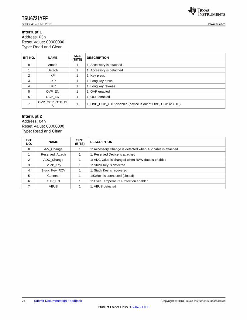
Interrupt 1Address: 03hReset Value: 00000000Type: Read and Clear
SIZEBIT NO. NAME DESCRIPTION(BITS)
0 Attach 1 1: Accessory is attached
1 Detach 1 1: Accessory is detached
2 KP 1 1: Key press
3 LKP 1 1: Long key press
4 LKR 1 1: Long key release
5 OVP_EN 1 1: OVP enabled
6 OCP_EN 1 1: OCP enabled
OVP_OCP_OTP_DI7 1 1: OVP_OCP_OTP disabled (device is out of OVP, OCP or OTP)S
Interrupt 2Address: 04hReset Value: 00000000Type: Read and Clear
BIT SIZENAME DESCRIPTIONNO. (BITS)
0 A/V_Change 1 1: Accessory Change is detected when A/V cable is attached
1 Reserved_Attach 1 1: Reserved Device is attached
2 ADC_Change 1 1: ADC value is changed when RAW data is enabled
3 Stuck_Key 1 1: Stuck Key is detected
4 Stuck_Key_RCV 1 1: Stuck Key is recovered
5 Connect 1 1:Switch is connected (closed)
6 OTP_EN 1 1: Over Temperature Protection enabled
7 VBUS 1 1: VBUS detected
24 Submit Documentation Feedback Copyright © 2013, Texas Instruments Incorporated
Product Folder Links :TSU6721YFF
TSU6721YFFwww.ti.com SCDS345 –JUNE 2013
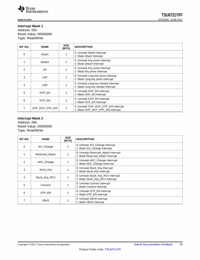
Interrupt Mask 1Address: 05hReset Value: 00000000Type: Read/Write
SIZEBIT NO. NAME DESCRIPTION(BITS)
0: Unmask Attach Interrupt0 Attach 1
1: Mask Attach Interrupt
0: Unmask Key press Interrupt1 Detach 1
1: Mask Detach Interrupt
0: Unmask Key press Interrupt2 KP 1
1: Mask Key press Interrupt
0: Unmask Long key press Interrupt3 LKP 1
1: Mask Long key press Interrupt
0: Unmask Long key release Interrupt4 LKR 1
1: Mask Long key release Interrupt
0: Unmask OVP_EN Interrupt5 OVP_EN 1
1: Mask OVP_EN Interrupt
0: Unmask OCP_EN Interrupt6 OCP_EN 1
1: Mask OCP_EN Interrupt
0: Unmask OVP_OCP_OTP_DIS Interrupt7 OVP_OCP_OTP_DIS 1
1: Mask OVP_OCP_OTP_DIS Interrupt
Interrupt Mask 2Address: 06hReset Value: 00000000Type: Read/Write
SIZEBIT NO. NAME DESCRIPTION(BITS)
0: Unmask A/V_Change Interrupt0 A/V_Change 1
1: Mask A/V_Change Interrupt
0: Unmask Reserved_Attach Interrupt1 Reserved_Attach 1
1: Mask Reserved_Attach Interrupt
0: Unmask ADC_Change Interrrupt2 ADC_Change 1
1: Mask ADC_Change Interrrupt
0: Unmask Stuck_Key Interrupt3 Stuck_Key 1
1: Mask Stuck_Key Interrupt
0: Unmask Stuck_Key_RCV Interrupt4 Stuck_Key_RCV 1
1: Mask Stuck_Key_RCV Interrupt
0: Unmask Connect Interrupt5 Connect 1
1: Mask Connect Interrupt
0: Unmask OTP_EN Interrupt6 OTP_EN 1
1: Mask OTP_EN Interrupt
0: Unmask VBUS Interrupt7 VBUS 1
1: Mask VBUS Interrupt
Copyright © 2013, Texas Instruments Incorporated Submit Documentation Feedback 25
Product Folder Links :TSU6721YFF
TSU6721YFFSCDS345 –JUNE 2013 www.ti.com
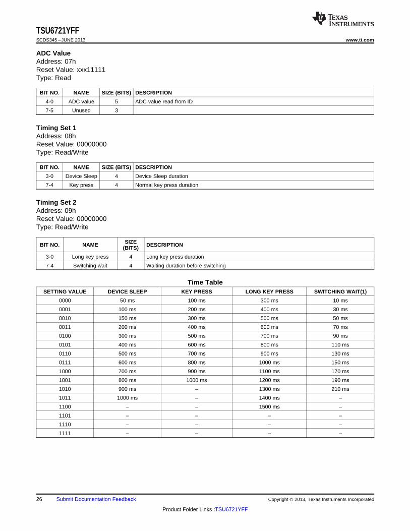
ADC ValueAddress: 07hReset Value: xxx11111Type: Read
BIT NO. NAME SIZE (BITS) DESCRIPTION
4-0 ADC value 5 ADC value read from ID
7-5 Unused 3
Timing Set 1Address: 08hReset Value: 00000000Type: Read/Write
BIT NO. NAME SIZE (BITS) DESCRIPTION
3-0 Device Sleep 4 Device Sleep duration
7-4 Key press 4 Normal key press duration
Timing Set 2Address: 09hReset Value: 00000000Type: Read/Write
SIZEBIT NO. NAME DESCRIPTION(BITS)
3-0 Long key press 4 Long key press duration
7-4 Switching wait 4 Waiting duration before switching
Time TableSETTING VALUE DEVICE SLEEP KEY PRESS LONG KEY PRESS SWITCHING WAIT(1)
0000 50 ms 100 ms 300 ms 10 ms
0001 100 ms 200 ms 400 ms 30 ms
0010 150 ms 300 ms 500 ms 50 ms
0011 200 ms 400 ms 600 ms 70 ms
0100 300 ms 500 ms 700 ms 90 ms
0101 400 ms 600 ms 800 ms 110 ms
0110 500 ms 700 ms 900 ms 130 ms
0111 600 ms 800 ms 1000 ms 150 ms
1000 700 ms 900 ms 1100 ms 170 ms
1001 800 ms 1000 ms 1200 ms 190 ms
1010 900 ms – 1300 ms 210 ms
1011 1000 ms – 1400 ms –
1100 – – 1500 ms –
1101 – – – –
1110 – – – –
1111 – – – –
26 Submit Documentation Feedback Copyright © 2013, Texas Instruments Incorporated
Product Folder Links :TSU6721YFF

TSU6721YFFwww.ti.com SCDS345 –JUNE 2013
Device Type 1Address: 0AhReset Value: 00000000Type: Read
BIT NAME SIZE DESCRIPTIONNO. (BITS)
0 Audio type 1 1 Audio device type 1
1 Audio type 2 1 Audio device type 2
2 USB 1 USB host
3 UART 1 UART
4 Type1/Type2 1 Type1/Type2 Charger
5 CDP 1 Charging Downstream Port (USB Host Hub Charger)
6 DCP 1 Dedicated Charging Port
7 USB OTG 1 USB on-the-go device
Device Type 2Address: 0BhReset Value: 00000000Type: Read
BIT NO. NAME SIZE (BITS) DESCRIPTION
0 JIG_USB_ON 1 Factory mode cable
1 JIG_USB_OFF 1 Factory mode cable
2 JIG_UART_ON 1 Factory mode cable
3 JIG_UART_OFF 1 Factory mode cable
4 PPD 1 Phone-powered device
5 TTY 1 TTY converter
6 A/V 1 A/V Cable
7 Audio Type 3 1 Audio device type 3
Copyright © 2013, Texas Instruments Incorporated Submit Documentation Feedback 27
Product Folder Links :TSU6721YFF

TSU6721YFFSCDS345 –JUNE 2013 www.ti.com
Button 1Address: 0ChReset Value: 00000000Type: Read and Clear
BIT NO. NAME SIZE (BITS) DESCRIPTION
0 Send_End 1 Send_End key is pressed
1 1 1 Number 1 key is pressed
2 2 1 Number 2 key is pressed
3 3 1 Number 3 key is pressed
4 4 1 Number 4 key is pressed
5 5 1 Number 5 key is pressed
6 6 1 Number 6 key is pressed
7 7 1 Number 7 key is pressed
Button 2Address: 0DhReset Value: x0000000Type: Read and Clear
BIT NO. NAME SIZE (BITS) DESCRIPTION
0 8 1 Number 8 key is pressed
1 9 1 Number 9 key is pressed
2 10 1 Number 10 key is pressed
3 11 1 Number 11 key is pressed
4 12 1 Number 12 key is pressed
5 Error 1 Error key is pressed
6 Unknown 1 Unknown key is pressed
7 Unused 1
28 Submit Documentation Feedback Copyright © 2013, Texas Instruments Incorporated
Product Folder Links :TSU6721YFF

TSU6721YFFwww.ti.com SCDS345 –JUNE 2013
Manual S/W 1Address: 13hReset Value: 00000000Type: Read/Write
BIT NAME SIZE (BITS) DESCRIPTIONNO.
1-0 VBUS Switching 2 00: Open all switch01: VBUS is connected to VBUS_OUT (charger)10: VBUS is connected to MIC
4-2 DP Switching 3 000: Open all switch001: DP is connected to DP_HT of USB port010: DP is connected to S_R011: DP is connected to RxD of UART100: Reserved 101: DP is connected to MIC110-111: Reserved
7-5 DM Switching 3 000: Open all switch001: DM is connected to DM_HT of USB port010: DM is connected to S_L011: DM is connected to TxD of UART100-111: Reserved
Manual S/W 2Address: 14hReset Value: xxx00000Type: Read/Write
BIT NAME SIZE (BITS) DESCRIPTIONNO.
1-0 ID Switching 2 00: Open all switch01: Reserved10: ID is connected to IDBP11: Reserved
2 JIG 1 0: Low (JIG OFF)1: High (JIG ON)
3 BOOT 1 0: Low (BOOT OFF)1: High (BOOT ON)
4 ISET 1 0: Low (ISET OFF)1: High (ISET ON)
7-5 Unused 3
Copyright © 2013, Texas Instruments Incorporated Submit Documentation Feedback 29
Product Folder Links :TSU6721YFF

TSU6721YFFSCDS345 –JUNE 2013 www.ti.com
Device Type 3Address: 15hReset Value: x000x000Type: Read
BIT NAME SIZE (BITS) DESCRIPTIONNO.
0 MHL 1 MHL device detected
1 VBUS Debounce 1 This bit goes high after the 8ms VBUS debounce time
2 VBUS Non- 1 A non-standard charger device detected. This bit goes high after BCDv1.2 timer expiresStandard
3 Unused 1
4 A/V VBUS 1 A/V Dock with VBUS connected
5 Apple Chg 1 Apple Charger
6 U200 Chg 1 U200 Charger
7 Video 1 75 Ohm video cable
ResetAddress:1BhReset Value: xxxxxxx0Type: Write
BIT NO. NAME SIZE (BITS) DESCRIPTION
0 Reset 1 Manual reset on device
7-1 Unused 6
30 Submit Documentation Feedback Copyright © 2013, Texas Instruments Incorporated
Product Folder Links :TSU6721YFF
TSU6721YFFwww.ti.com SCDS345 –JUNE 2013
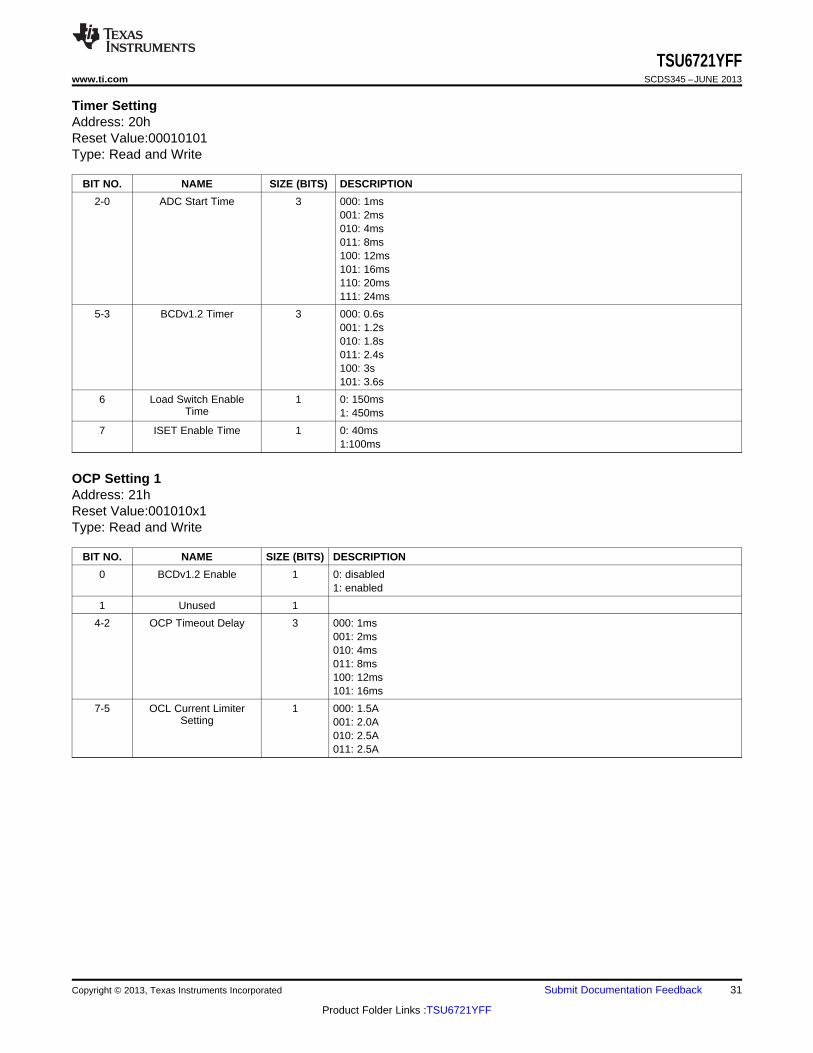
Timer SettingAddress: 20hReset Value:00010101Type: Read and Write
BIT NO. NAME SIZE (BITS) DESCRIPTION
2-0 ADC Start Time 3 000: 1ms001: 2ms010: 4ms011: 8ms100: 12ms101: 16ms110: 20ms111: 24ms
5-3 BCDv1.2 Timer 3 000: 0.6s001: 1.2s010: 1.8s011: 2.4s100: 3s101: 3.6s
6 Load Switch Enable 1 0: 150msTime 1: 450ms
7 ISET Enable Time 1 0: 40ms1:100ms
OCP Setting 1Address: 21hReset Value:001010x1Type: Read and Write
BIT NO. NAME SIZE (BITS) DESCRIPTION
0 BCDv1.2 Enable 1 0: disabled1: enabled
1 Unused 1
4-2 OCP Timeout Delay 3 000: 1ms001: 2ms010: 4ms011: 8ms100: 12ms101: 16ms
7-5 OCL Current Limiter 1 000: 1.5ASetting 001: 2.0A
010: 2.5A011: 2.5A
Copyright © 2013, Texas Instruments Incorporated Submit Documentation Feedback 31
Product Folder Links :TSU6721YFF
TSU6721YFFSCDS345 –JUNE 2013 www.ti.com
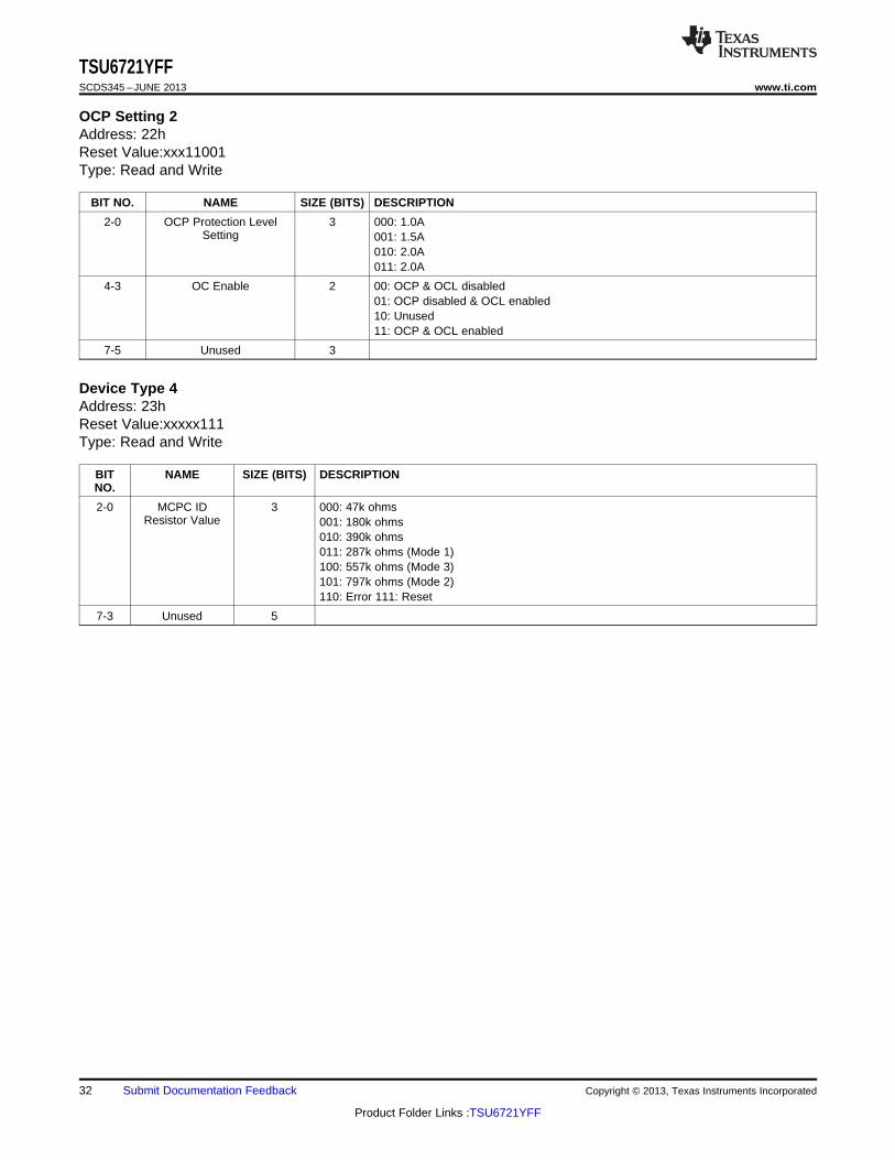
OCP Setting 2Address: 22hReset Value:xxx11001Type: Read and Write
BIT NO. NAME SIZE (BITS) DESCRIPTION
2-0 OCP Protection Level 3 000: 1.0ASetting 001: 1.5A
010: 2.0A011: 2.0A
4-3 OC Enable 2 00: OCP & OCL disabled01: OCP disabled & OCL enabled10: Unused11: OCP & OCL enabled
7-5 Unused 3
Device Type 4Address: 23hReset Value:xxxxx111Type: Read and Write
BIT NAME SIZE (BITS) DESCRIPTIONNO.
2-0 MCPC ID 3 000: 47k ohmsResistor Value 001: 180k ohms
010: 390k ohms011: 287k ohms (Mode 1)100: 557k ohms (Mode 3)101: 797k ohms (Mode 2)110: Error 111: Reset
7-3 Unused 5
32 Submit Documentation Feedback Copyright © 2013, Texas Instruments Incorporated
Product Folder Links :TSU6721YFF
PMIC
MICRO
USB
V+
DN
DP
ID
GND
TSU6721
INTB
DP_HOST
DM_HOST
RxD
TxD
VBUS
DM
DP
ID
GND
AP ORBASEBAND
2.2Ω
2.2Ω
1pF
ESD2.2Ω
1pF
ESD2.2Ω
1pF
ESD
1µF
1.7~ 3.6V
SCL
SDA
JIG
INTB
DP_HOST
DM_HOST
RxD
TxD
SCL
SDA
JIG
1kΩ ~
10kΩ
VDDIO VDDIO
VBAT
1µF~
10µF
1µF~
10µF
Battery
BOOTBOOT
VBAT
1kΩ ~
10kΩ
1kΩ ~
10kΩ
AUDIO
CODECS_L
MIC
S_R
OUT
10µF
MIC_BIAS
0.1µF
0.1µF
0.1µF
ISETISET
ISET Resistor
1pF~
10pF
ESD
IDBPIDBP
(optional )
TSU6721YFFwww.ti.com SCDS345 –JUNE 2013
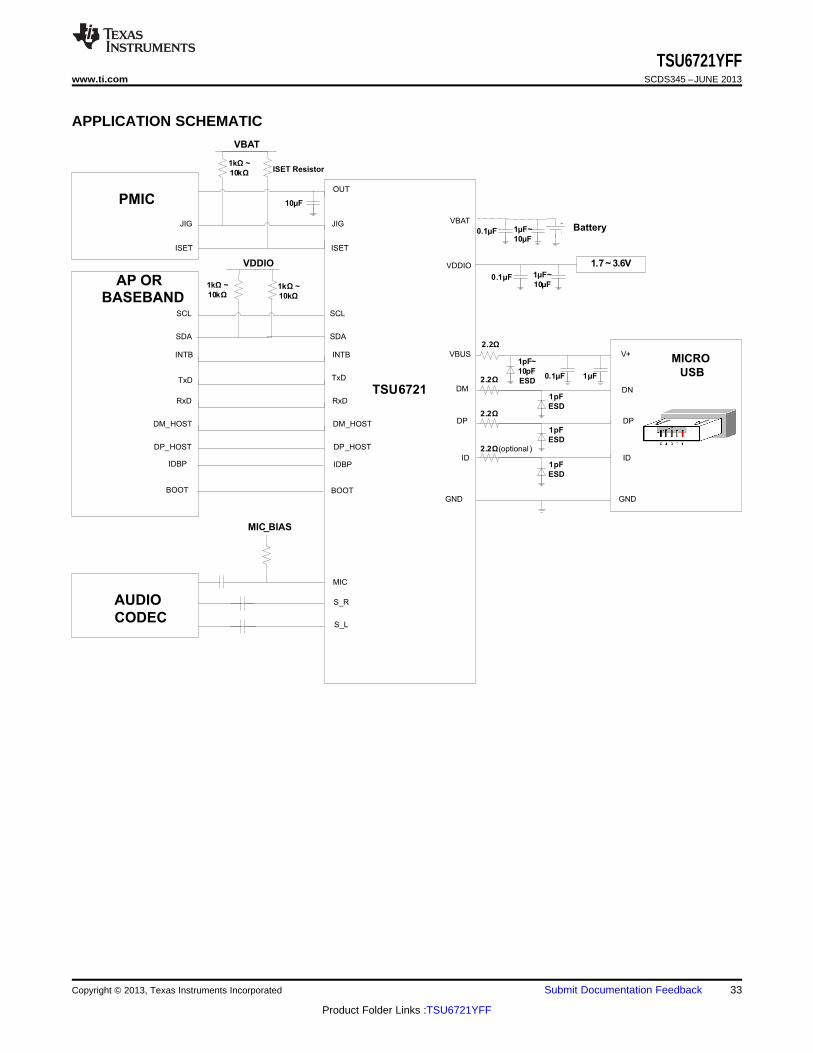
APPLICATION SCHEMATIC
Copyright © 2013, Texas Instruments Incorporated Submit Documentation Feedback 33
Product Folder Links :TSU6721YFF

TSU6721YFFSCDS345 –JUNE 2013 www.ti.com
CRITICAL COMPONENTS
PIN NAME PIN NUMBER CRITICAL COMPONENT
VBUS A5, B5 2.2 ΩD3 1 µF~10 µF
VDDIO0.1 µF
1 µF~10 µF
VBAT C3 Battery
0.1 µF
JIG E3 1 kΩ~10 kΩ2.2 kΩ
MIC B310 µF
ISET A2 Resistor determined by Battery Charger
S_R D4 220 µF (1)
S_L C4 220 µF (1)
OUT A4, B4 10 µF
SCL A1 1 kΩ~10 kΩSDA B1 1 kΩ~10 kΩ
2.2 ΩDM C5
ESD Protection Diode
2.2 ΩDP D5
ESD Protection Diode
2.2 Ω (1)
ID E5ESD Protection Diode
(1) Optional Components
SCHEMATIC GUIDELINES1. VBUS, VDDIO, and VBAT require decoupling capacitors to reduce noise from circuit elements. The
capacitors act as a shunt to block off the noise. The 0.1µF capacitor smoothes out high frequencies and hasa lower series inductance. The 1µF~10µF and 1µF capacitors smooth out the lower frequencies and have amuch higher series inductance. Placing both decoupling capacitors will provide better load regulation acrossthe frequency spectrum.
2. OUT requires a 10µF load capacitor to prevent sudden increases of voltage on the pin during charging3. JIG is an open-drain output and therefore requires a 1kΩ ~ 10kΩ pull-up resistor to VBAT4. ISET is an open drain output. It can be used by the battery charger to set the input current limit with a series
resistor (for example 75Ω determined by the charger)5. SCL and SDA require 1kΩ ~ 10kΩ pull-up resistors to VDDIO to prevent floating inputs6. Depending on the codec used, S_R and S_L may require DC blocking capacitors as high as 220µF. The
capacitor might not be needed if the codec has the capability to provide ground centered signals.7. Mic requires a 2.2kΩ pull-up resistor to MIC_BIAS to provide DC bias for the microphone. Additionally the
10µF capacitor is required to block the DC signals from MIC_BIAS to the Audio Codec8. VBUS, DM and DP are recommended to have an external resistor 2.2Ω to provide extra ballasting to protect
the chip and internal circuitry(a) For ID, if there is less stress on the ID pin then the external 2.2Ω resistor is optional
34 Submit Documentation Feedback Copyright © 2013, Texas Instruments Incorporated
Product Folder Links :TSU6721YFF

TSU6721YFFwww.ti.com SCDS345 –JUNE 2013
9. DDM, DP, and ID are rated for 6kV IEC contact discharge protection. To prevent failure in case of an IECcontact discharge of 8kV or greater, it is recommended to have an external ESD Protection Diode (~1pF ofcapacitance allowed) rated for greater than 8kV IEC protection. It is also recommended to have an externalESD Protection Diode to prevent DP and DM from failure in the event of EOS related to electrical surgepropagated downstream from the AC power supply
10. VBUS is rated for 6kV IEC contact discharge protection. To prevent failure in case of an IEC contactdischarge of 8kV or greater, it is recommended to have an external ESD Protection Diode (~1pF ofcapacitance allowed) rated for greater than 8kV IEC protection. It is also recommended to have an externalESD Protection Diode to prevent VBUS from failure in the event of EOS related to electrical surgepropagated downstream from the AC power supply.
PCB ROUTING GUIDELINES
Routing Guidelines for USB Signal Integrity1. All the USB lines DP_CON, DM_CON, DP_HT, DM_HT, TxD and RxD
(a) Must have 45Ω single ended characteristic impedance(b) Must have 90Ω differential ended impedance(c) To fulfill USB 2.0 requirements
2. TSU6721 location(a) Close to the USB connector as possible(b) The distance between the USB controller and the device less than 1 inch(c) Shorter length of the trace will reduce effect of stray noise and radiate less EMI
3. Minimize use of VIAs for USB related signals(a) Differential transmission lines should be matched as close as possible(b) No VIAs for optimum USB2.0 performance
Copyright © 2013, Texas Instruments Incorporated Submit Documentation Feedback 35
Product Folder Links :TSU6721YFF

PACKAGE OPTION ADDENDUM
www.ti.com 2-Jul-2013
Addendum-Page 1
PACKAGING INFORMATION
Orderable Device Status(1)
Package Type PackageDrawing
Pins PackageQty
Eco Plan(2)
Lead/Ball Finish MSL Peak Temp(3)
Op Temp (°C) Device Marking(4/5)
Samples
TSU6721YFFR ACTIVE DSBGA YFF 25 3000 Green (RoHS& no Sb/Br)
SNAGCU Level-1-260C-UNLIM -40 to 85 TSU6721
(1) The marketing status values are defined as follows:ACTIVE: Product device recommended for new designs.LIFEBUY: TI has announced that the device will be discontinued, and a lifetime-buy period is in effect.NRND: Not recommended for new designs. Device is in production to support existing customers, but TI does not recommend using this part in a new design.PREVIEW: Device has been announced but is not in production. Samples may or may not be available.OBSOLETE: TI has discontinued the production of the device.
(2) Eco Plan - The planned eco-friendly classification: Pb-Free (RoHS), Pb-Free (RoHS Exempt), or Green (RoHS & no Sb/Br) - please check http://www.ti.com/productcontent for the latest availabilityinformation and additional product content details.TBD: The Pb-Free/Green conversion plan has not been defined.Pb-Free (RoHS): TI's terms "Lead-Free" or "Pb-Free" mean semiconductor products that are compatible with the current RoHS requirements for all 6 substances, including the requirement thatlead not exceed 0.1% by weight in homogeneous materials. Where designed to be soldered at high temperatures, TI Pb-Free products are suitable for use in specified lead-free processes.Pb-Free (RoHS Exempt): This component has a RoHS exemption for either 1) lead-based flip-chip solder bumps used between the die and package, or 2) lead-based die adhesive used betweenthe die and leadframe. The component is otherwise considered Pb-Free (RoHS compatible) as defined above.Green (RoHS & no Sb/Br): TI defines "Green" to mean Pb-Free (RoHS compatible), and free of Bromine (Br) and Antimony (Sb) based flame retardants (Br or Sb do not exceed 0.1% by weightin homogeneous material)
(3) MSL, Peak Temp. -- The Moisture Sensitivity Level rating according to the JEDEC industry standard classifications, and peak solder temperature.
(4) There may be additional marking, which relates to the logo, the lot trace code information, or the environmental category on the device.
(5) Multiple Device Markings will be inside parentheses. Only one Device Marking contained in parentheses and separated by a "~" will appear on a device. If a line is indented then it is a continuationof the previous line and the two combined represent the entire Device Marking for that device.
Important Information and Disclaimer:The information provided on this page represents TI's knowledge and belief as of the date that it is provided. TI bases its knowledge and belief on informationprovided by third parties, and makes no representation or warranty as to the accuracy of such information. Efforts are underway to better integrate information from third parties. TI has taken andcontinues to take reasonable steps to provide representative and accurate information but may not have conducted destructive testing or chemical analysis on incoming materials and chemicals.TI and TI suppliers consider certain information to be proprietary, and thus CAS numbers and other limited information may not be available for release.
In no event shall TI's liability arising out of such information exceed the total purchase price of the TI part(s) at issue in this document sold by TI to Customer on an annual basis.

www.ti.com
PACKAGE OUTLINE
C0.625 MAX
0.300.12
1.6TYP
1.6 TYP
0.4 TYP
0.4 TYP25X 0.30.2
B E A
D
4223786/A 06/2017
DSBGA - 0.625 mm max heightYFF0025DIE SIZE BALL GRID ARRAY
NOTES: 1. All linear dimensions are in millimeters. Any dimensions in parenthesis are for reference only. Dimensioning and tolerancing per ASME Y14.5M. 2. This drawing is subject to change without notice.
BUMP A1CORNER
SEATING PLANEBALL TYP
0.05 C
A
B
C
D
1 2 3
0.015 C A B
E
54
SYMM
SYMM
SCALE 6.000
D: Max =
E: Max =
2.096 mm, Min =
2.096 mm, Min =
2.036 mm
2.036 mm

www.ti.com
EXAMPLE BOARD LAYOUT
25X ( 0.23)(0.4) TYP
(0.4) TYP
( 0.23)METAL
0.05 MAX
SOLDER MASKOPENING
METAL UNDERSOLDER MASK
( 0.23)SOLDER MASKOPENING
0.05 MIN
4223786/A 06/2017
DSBGA - 0.625 mm max heightYFF0025DIE SIZE BALL GRID ARRAY
NOTES: (continued) 3. Final dimensions may vary due to manufacturing tolerance considerations and also routing constraints. For more information, see Texas Instruments literature number SNVA009 (www.ti.com/lit/snva009).
SYMM
SYMM
LAND PATTERN EXAMPLEEXPOSED METAL SHOWN
SCALE:25X
A
B
C
D
1 2 3 4 5
E
NON-SOLDER MASKDEFINED
(PREFERRED)
SOLDER MASK DETAILSNOT TO SCALE
EXPOSED METAL
SOLDER MASKDEFINED
EXPOSED METAL

www.ti.com
EXAMPLE STENCIL DESIGN
(0.4) TYP
(0.4) TYP
25X ( 0.25)(R0.05) TYP
METALTYP
4223786/A 06/2017
DSBGA - 0.625 mm max heightYFF0025DIE SIZE BALL GRID ARRAY
NOTES: (continued) 4. Laser cutting apertures with trapezoidal walls and rounded corners may offer better paste release.
SYMM
SYMM
SOLDER PASTE EXAMPLEBASED ON 0.1 mm THICK STENCIL
SCALE:30X
A
B
C
D
1 2 3
E
4 5

IMPORTANT NOTICE
Texas Instruments Incorporated (TI) reserves the right to make corrections, enhancements, improvements and other changes to itssemiconductor products and services per JESD46, latest issue, and to discontinue any product or service per JESD48, latest issue. Buyersshould obtain the latest relevant information before placing orders and should verify that such information is current and complete.TI’s published terms of sale for semiconductor products (http://www.ti.com/sc/docs/stdterms.htm) apply to the sale of packaged integratedcircuit products that TI has qualified and released to market. Additional terms may apply to the use or sale of other types of TI products andservices.Reproduction of significant portions of TI information in TI data sheets is permissible only if reproduction is without alteration and isaccompanied by all associated warranties, conditions, limitations, and notices. TI is not responsible or liable for such reproduceddocumentation. Information of third parties may be subject to additional restrictions. Resale of TI products or services with statementsdifferent from or beyond the parameters stated by TI for that product or service voids all express and any implied warranties for theassociated TI product or service and is an unfair and deceptive business practice. TI is not responsible or liable for any such statements.Buyers and others who are developing systems that incorporate TI products (collectively, “Designers”) understand and agree that Designersremain responsible for using their independent analysis, evaluation and judgment in designing their applications and that Designers havefull and exclusive responsibility to assure the safety of Designers' applications and compliance of their applications (and of all TI productsused in or for Designers’ applications) with all applicable regulations, laws and other applicable requirements. Designer represents that, withrespect to their applications, Designer has all the necessary expertise to create and implement safeguards that (1) anticipate dangerousconsequences of failures, (2) monitor failures and their consequences, and (3) lessen the likelihood of failures that might cause harm andtake appropriate actions. Designer agrees that prior to using or distributing any applications that include TI products, Designer willthoroughly test such applications and the functionality of such TI products as used in such applications.TI’s provision of technical, application or other design advice, quality characterization, reliability data or other services or information,including, but not limited to, reference designs and materials relating to evaluation modules, (collectively, “TI Resources”) are intended toassist designers who are developing applications that incorporate TI products; by downloading, accessing or using TI Resources in anyway, Designer (individually or, if Designer is acting on behalf of a company, Designer’s company) agrees to use any particular TI Resourcesolely for this purpose and subject to the terms of this Notice.TI’s provision of TI Resources does not expand or otherwise alter TI’s applicable published warranties or warranty disclaimers for TIproducts, and no additional obligations or liabilities arise from TI providing such TI Resources. TI reserves the right to make corrections,enhancements, improvements and other changes to its TI Resources. TI has not conducted any testing other than that specificallydescribed in the published documentation for a particular TI Resource.Designer is authorized to use, copy and modify any individual TI Resource only in connection with the development of applications thatinclude the TI product(s) identified in such TI Resource. NO OTHER LICENSE, EXPRESS OR IMPLIED, BY ESTOPPEL OR OTHERWISETO ANY OTHER TI INTELLECTUAL PROPERTY RIGHT, AND NO LICENSE TO ANY TECHNOLOGY OR INTELLECTUAL PROPERTYRIGHT OF TI OR ANY THIRD PARTY IS GRANTED HEREIN, including but not limited to any patent right, copyright, mask work right, orother intellectual property right relating to any combination, machine, or process in which TI products or services are used. Informationregarding or referencing third-party products or services does not constitute a license to use such products or services, or a warranty orendorsement thereof. Use of TI Resources may require a license from a third party under the patents or other intellectual property of thethird party, or a license from TI under the patents or other intellectual property of TI.TI RESOURCES ARE PROVIDED “AS IS” AND WITH ALL FAULTS. TI DISCLAIMS ALL OTHER WARRANTIES ORREPRESENTATIONS, EXPRESS OR IMPLIED, REGARDING RESOURCES OR USE THEREOF, INCLUDING BUT NOT LIMITED TOACCURACY OR COMPLETENESS, TITLE, ANY EPIDEMIC FAILURE WARRANTY AND ANY IMPLIED WARRANTIES OFMERCHANTABILITY, FITNESS FOR A PARTICULAR PURPOSE, AND NON-INFRINGEMENT OF ANY THIRD PARTY INTELLECTUALPROPERTY RIGHTS. TI SHALL NOT BE LIABLE FOR AND SHALL NOT DEFEND OR INDEMNIFY DESIGNER AGAINST ANY CLAIM,INCLUDING BUT NOT LIMITED TO ANY INFRINGEMENT CLAIM THAT RELATES TO OR IS BASED ON ANY COMBINATION OFPRODUCTS EVEN IF DESCRIBED IN TI RESOURCES OR OTHERWISE. IN NO EVENT SHALL TI BE LIABLE FOR ANY ACTUAL,DIRECT, SPECIAL, COLLATERAL, INDIRECT, PUNITIVE, INCIDENTAL, CONSEQUENTIAL OR EXEMPLARY DAMAGES INCONNECTION WITH OR ARISING OUT OF TI RESOURCES OR USE THEREOF, AND REGARDLESS OF WHETHER TI HAS BEENADVISED OF THE POSSIBILITY OF SUCH DAMAGES.Unless TI has explicitly designated an individual product as meeting the requirements of a particular industry standard (e.g., ISO/TS 16949and ISO 26262), TI is not responsible for any failure to meet such industry standard requirements.Where TI specifically promotes products as facilitating functional safety or as compliant with industry functional safety standards, suchproducts are intended to help enable customers to design and create their own applications that meet applicable functional safety standardsand requirements. Using products in an application does not by itself establish any safety features in the application. Designers mustensure compliance with safety-related requirements and standards applicable to their applications. Designer may not use any TI products inlife-critical medical equipment unless authorized officers of the parties have executed a special contract specifically governing such use.Life-critical medical equipment is medical equipment where failure of such equipment would cause serious bodily injury or death (e.g., lifesupport, pacemakers, defibrillators, heart pumps, neurostimulators, and implantables). Such equipment includes, without limitation, allmedical devices identified by the U.S. Food and Drug Administration as Class III devices and equivalent classifications outside the U.S.TI may expressly designate certain products as completing a particular qualification (e.g., Q100, Military Grade, or Enhanced Product).Designers agree that it has the necessary expertise to select the product with the appropriate qualification designation for their applicationsand that proper product selection is at Designers’ own risk. Designers are solely responsible for compliance with all legal and regulatoryrequirements in connection with such selection.Designer will fully indemnify TI and its representatives against any damages, costs, losses, and/or liabilities arising out of Designer’s non-compliance with the terms and provisions of this Notice.
Mailing Address: Texas Instruments, Post Office Box 655303, Dallas, Texas 75265Copyright © 2018, Texas Instruments Incorporated