mechanical workshop - griffith university · generic skills for microelectronic engineers...
TRANSCRIPT

Generic Skills for Microelectronic Engineers
Mechanical WorkshopMEE1010
2003
This session is available at http://maxwell.me.gu.edu.au/sok/gs/gs.html

Aim
To discuss some of the common workshop processes that electronics engineers will be
expected to deal with.
Outline
• Metal instrument cases
• PCB manufacture
• Electronic assembly

Metal Instrument Cases
Nearly all electronic circuits need to be housed in some form of enclosure.
This is to provide
• protection for the delicate electronic circuit• protection to the user from hazardous voltages• shielding from external electromagnetic fields • shielding to prevent the radiation of EM fields
The first 2 requirements may be achieved through the use of plastic enclosures. The last 2 requirements however normally require the enclosure to be manufactured from metal.
It is therefore quite common for an electronics engineer to be involved in the fabrication of metal enclosures. Some metal enclosures and most plastic enclosures will be manufactured by specialists, but may be overseen by you (the engineer).

Diecast enclosures
Can be general purpose or made specifically for a given application or custom made for your product. Custom die style enclosures are VERY expensive in small quantities. Manufacture of the dies may cost 10’s of thousands of dollars.

Folded enclosures
The cheapest types of metal enclosures are usually folded sheet metal. Many larger engineering firms have workshop facilities to make these types of enclosures.
You will be making a folded aluminium case for your power supply unit.
Lets step through the process and see the tools required.
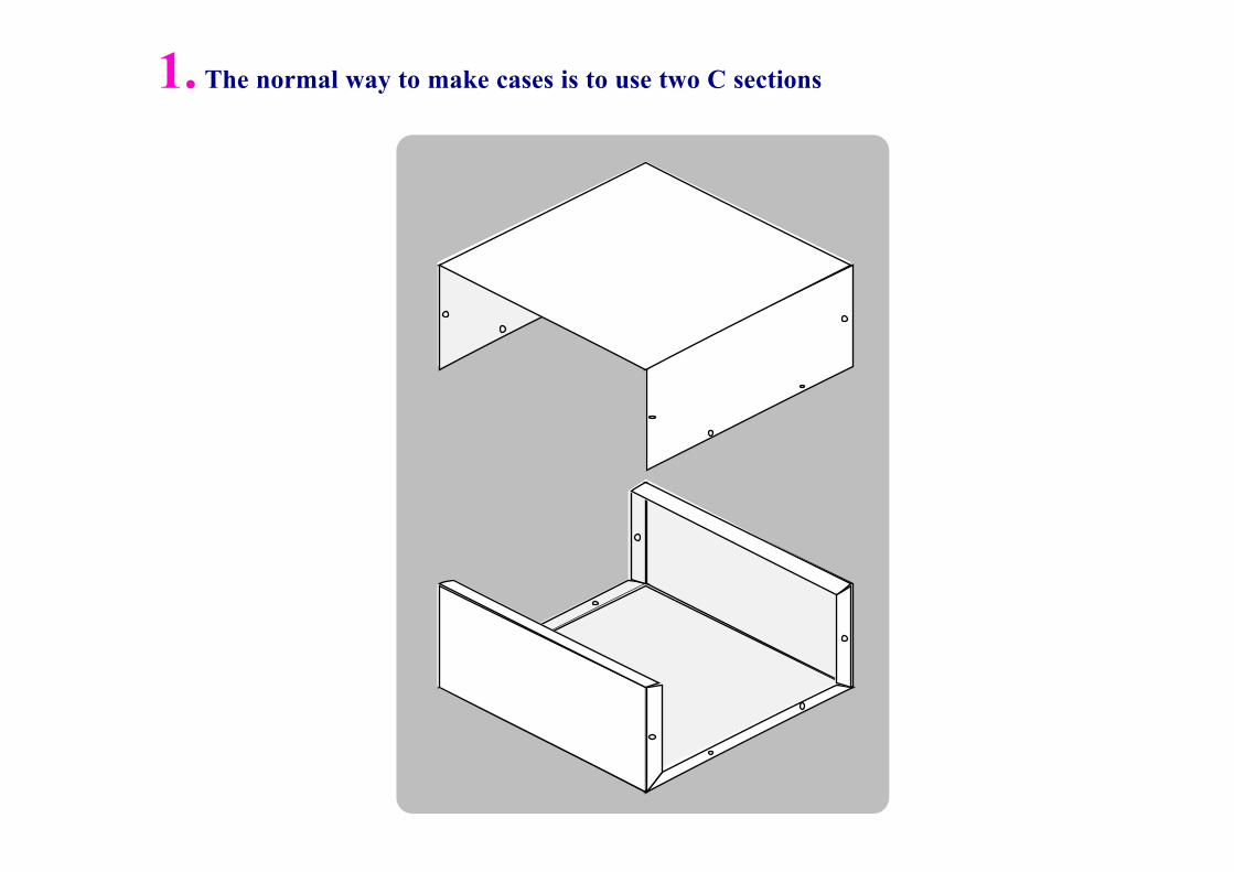
1. The normal way to make cases is to use two C sections

2. The base and lid are cut from a sheet. The sheet must be marked out completely to
minimise wastage.
Folds
Guillotine Cuts
Waste
BOTTOM TOP
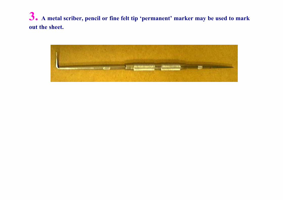
3. A metal scriber, pencil or fine felt tip ‘permanent’ marker may be used to mark
out the sheet.

4. It must then be cut to size. A sheet metal guillotine is used to do this.
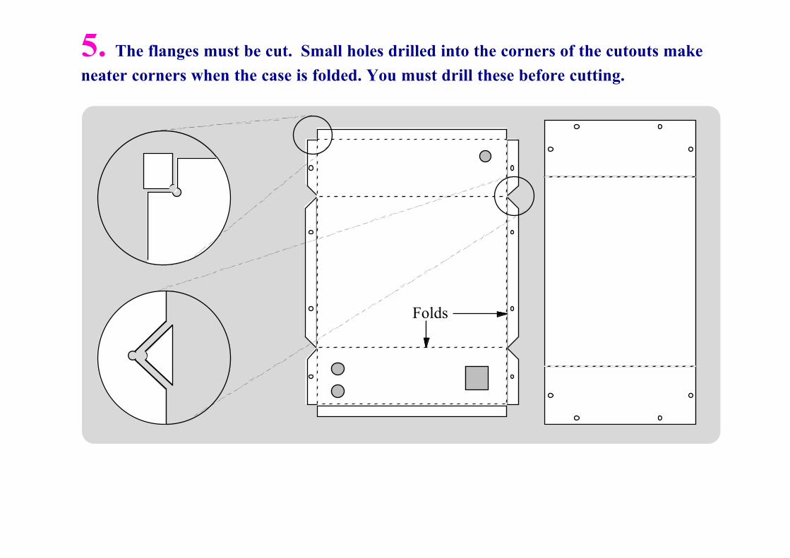
5. The flanges must be cut. Small holes drilled into the corners of the cutouts make
neater corners when the case is folded. You must drill these before cutting.
Folds
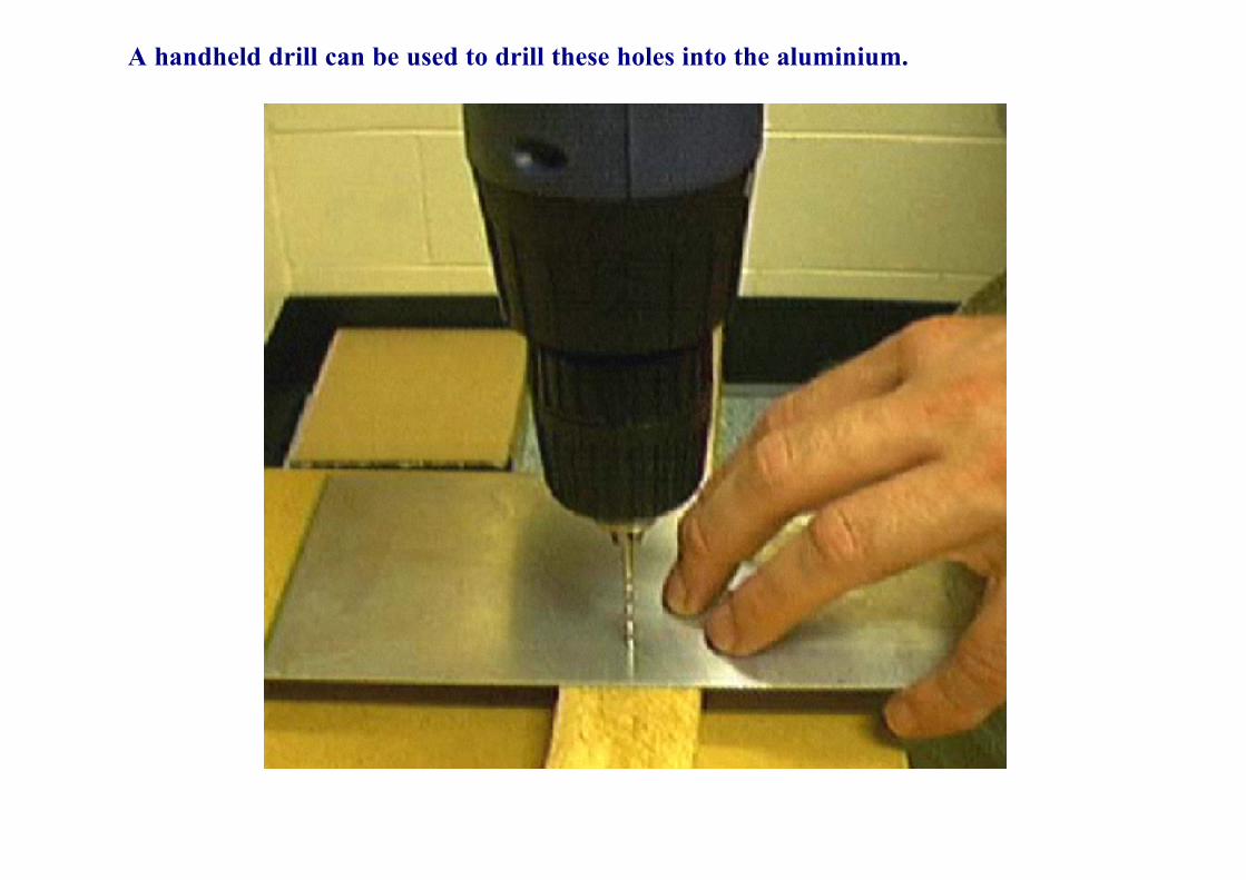
A handheld drill can be used to drill these holes into the aluminium.

6. The cutouts are made with tin snips. Snips come in left, right and straight cut.

7. Large holes should be centre punched before drilling. If using a manual punch all
sizes should be centre punched. You will be provided with an auto punch that does not require a hammer. Small holes can be drilled in soft metal (such as aluminium) without centre punching.
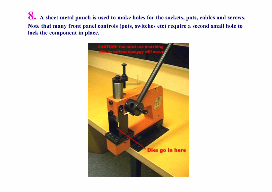
8. A sheet metal punch is used to make holes for the sockets, pots, cables and screws.
Note that many front panel controls (pots, switches etc) require a second small hole to lock the component in place.

9. A metal folder is used to fold up the case. The long edge folds must be completed
first followed by the end edges, then the two centre folds ;-)NOTE: It is possible to get your fingers into the metal folder when it is open. Take great care not to do this as severe injuries may occur if the machine is operated.

10. The small holes for the case screws are drilled when the case is assembled. In soft
material like aluminium these holes are often only centre-punched if sharp self tapping screws are used.
Printed Circuit Board Manufacture
• PCBs are normally made of fibreglass board which is completely coated on one side (single sided PCB) or both sides (double sided PCB) with copper.
• Some special high frequency boards are made of exotic materials (Alumina, Duroid etc)
• High power boards have thicker copper to handle the higher currents. It is measured in weight per square metre. (Normal is usually 1 oz/metre2)
• To make a PCB the layer of copper must be removed in places and left intact in others to create the tracks that form the connections between the components mounted on the board.
• The steps involved are
• PCB track layout design• Transfer of design to PCB copper layer• Etching of copper layer• Cleaning and protection

PCB track layout
• You first must have a circuit diagram of the circuit you wish to build.
• The tracks on the PCB can be laid out manually, ie you decide where the components are to be placed on the board and you draw in the interconnecting tracks. This is normally done on a computer using special PCB software.
• The placement of the components and interconnections can also be done automatically with special auto-routing software. The circuit diagram needs to be supplied to the software.
• As most electronic components have multiples of 0.1 inch spacing between their legs we usually layout on a 0.05 inch grid. (Surface mount uses a much smaller grid 0.025” or less)
• Much of this software is very expensive, but some is free. Look on maxwell for links to free PCB layout software.
• A popular one is Easytrax (http://www.protel.com.au/etech/freeware_home.html)

PSU Schematic

PSU Overlay

PSU Artwork

Transfer of design to copper
• When manufactured commercially the circuit layout is printed onto the copper using an acid resistant ink.
• For prototypes or small runs a photographic process is used. A layer of acid resistant chemical is applied to the copper. It is called photoresist because it is light sensitive.
• There are 2 types of photoresist, positive and negative process. For one the resist will wash away if exposed to light and the other the resist will wash away if not exposed to light. Your therefore need a positive or negative image of the circuit track layout to expose the photoresist with for each process.
• The resist is usually most sensitive to UV light. Best results come from a UV lamp but the sun can be used. (Takes a lot longer)
• After exposure the resist is washed away with special developer.

On the cheap
You can transfer simple PCB layouts onto copper simply and easily for one off jobs.
• You must first reverse the artwork so that it appears as the view from the fibreglass side of the board.
• Print your PCB artwork using a laser printer
• Place the printout face down on the cleaned copper so it can’t slide about.
• Tell your mum you need to borrow her iron to do your shirts and iron the paper onto the copper.
• The toner will melt onto the copper.
• Wet the paper till soggy and carefully rub it off.
• The board can now be etched.

Etching• The PCB with photoresist is now placed into a bath of chemicals that will eat away all
the exposed copper, ie the copper not covered with resist.
• The common etchants are
Ferric Chloride [FeCl2]CORROSIVEBrown staining liquidWorks well at room temperature and even better when heated
Ammonium Persulphate [(NH4)2S2O8] CORROSIVE
Clear liquidNeeds to be heated above 60 degrees
NOTE: Both these chemicals will make a real mess of your mum’s kitchen.

Cleaning and Protection
Usually the holes are drilled at this stage before the resist is removed. A high speed drill with the appropriate drill bit is required.
The photoresist (or laserprinter toner) must now be removed. Photoresist is usually dissolved with the appropriate chemical. Toner can be removed with paint thinner.
The bare copper must be protected from oxidisation. Special spray coatings are available that protect the copper but allow soldering onto the surface. These coatings often contain rosin.

PCB Assembly
When assembling PCBs we normally start by examining the PCB to ensure there are no broken tracks or missing holes. If all is well and the board is clean or sprayed we begin soldering the components into place.
Components are normally mounted in order of height and delicateness (Many semiconductor devices can be destroyed by static charges if handled).
The order therefore usually goes as
• Links• Resistors• Capacitors• Semiconductors (Integrated Circuits ICs, transistors, diodes etc)• Hardware (Pots, switches, connectors)

Components should be mounted so that they are
• Neatly placed and not twisted• Mounted close to the PCB as possible• In such a position that the component value can be read easily• Placed so there is no strain on the component• Wires should be stripped flush with the top of the PCB
22m
F22
mF

Wiring to non PCB mounted components should be neatly run in ‘forms’.Cable ties or lacing should be used to bundle the forms.Low voltage terminations should be neatly soldered with no stress applied to the joint.High voltage terminations must be insulated with insulating tubing etc.
PCB