mlxxxx - images-na.ssl-images-amazon.com
TRANSCRIPT

MLX71121 300 to 930MHz
FSK/OOK Receiver
REVISION 013 - JUNE 13, 2017
3901071121
Features
Two RF inputs for antenna diversity, LNA cascading or differential feeding
Integrated IF filter
Integrated FSK and OOK demodulator
Fully integrated PLL-based synthesizer
Wide operating voltage
Very low standby current consumption
Low operating current consumption
Average and peak detection data slicer mode
Analog RSSI output with high dynamic range
Noise cancellation filter
MCU clock output
High frequency accuracy
32-pin QFN
Application Examples
Automotive RKE
TPMS
Smart metering (AMR)
Home and building automation
Consumer remote controls
Alarm and security systems
Low power telemetry systems
Garage and door openers
Pin Description
Ordering Code
Product Code Temperature Code Package Code Option Code Packing Form Code MLX71121 K LQ AAA-000 RE
Legend: Temperature Code: K for Temperature Range -40°C to 125°C Package Code: LQ for QFN Packing Form: RE for Reel
Ordering example: MLX71121KLQ-AAA-000-RE
General Description
The MLX71121 is a highly-integrated single-channel/dual-band RF receiver based on a double-conversion super-heterodyne architecture. It can receive FSK and OOK modulated signals. The IC is designed for gen-eral purpose applications for example in the European bands at 433MHz and 868MHz or for similar applica-tions in North America or Asia, for example at 315MHz or 915MHz.
MIX
O
IFA
P
IFA
N
VE
E
SL
CS
EL
DF
2
VC
C
MO
DS
EL
bottomtop
MLX71121LNAO1
LNAO2MIXN
MIXP
VEE
VEELNAI2
LNAI1 RSSI
DF1
DFO
PDP
PDN
CINT
SLC
VCC
DTA
O
CLK
O
LN
AS
EL
RF
SE
L
IFS
EL
RO
I
MLX71121 300 to 930MHz FSK/OOK Receiver
REVISION 013 - JUNE 13, 2017
3901071121
Contents
Features ..................................................................................................................................................... 1
Application Examples ................................................................................................................................. 1
Pin Description ........................................................................................................................................... 1
Ordering Code ............................................................................................................................................ 1
General Description ................................................................................................................................... 1
1. Theory of Operation ............................................................................................................................... 4
1.1. General................................................................................................................................................ 4
1.2. Technical Data Overview.................................................................................................................... 4
1.3. Block Diagram ..................................................................................................................................... 5
1.4. Operating Modes................................................................................................................................ 6
1.5. LNA Selection ...................................................................................................................................... 6
1.6. Mixer Section ...................................................................................................................................... 7
1.7. IF Filter ................................................................................................................................................ 7
1.8. IF Amplifier .......................................................................................................................................... 7
1.9. PLL Synthesizer ................................................................................................................................... 7
1.10. Reference Oscillator ......................................................................................................................... 8
1.11. Clock Output ..................................................................................................................................... 8
1.12. FSK Demodulator.............................................................................................................................. 8
1.13. Baseband Data Path ......................................................................................................................... 9
1.14. Data Filter ....................................................................................................................................... 10
1.15. Data Slicer ....................................................................................................................................... 10
1.15.1. Averaging Detection Mode ...................................................................................................... 11
1.15.2. Peak Detection Mode .............................................................................................................. 11
1.16. Data Output and Noise Cancellation Filter ................................................................................... 12
2. Functional Description ......................................................................................................................... 13
2.1. Frequency Planning .......................................................................................................................... 13
2.2. Calculation of Frequency Settings ................................................................................................... 14
2.3. Standard Frequency Plans ............................................................................................................... 15
2.4. 433/868MHz Frequency Diversity ................................................................................................... 15
3. Pin Definitions and Descriptions ........................................................................................................... 16
4. Technical Data ...................................................................................................................................... 20
4.1. Absolute Maximum Ratings ............................................................................................................. 20
4.2. Normal Operating Conditions .......................................................................................................... 20
MLX71121 300 to 930MHz FSK/OOK Receiver
REVISION 013 - JUNE 13, 2017
3901071121
4.3. DC Characteristics ............................................................................................................................ 21
4.4. AC System Characteristics ................................................................................................................ 22
4.5. External Components ....................................................................................................................... 23
5. Test Circuit ........................................................................................................................................... 24
5.1. Antenna Diversity Application Circuit ............................................................................................. 24
5.1.1. Component List for Fig. 11 ......................................................................................................... 25
6. Package Description ............................................................................................................................. 26
7. Standard Information Regarding Manufacturability of Melexis Products with Different Soldering Processes ....................................................... 27
8. ESD Precautions ................................................................................................................................... 27
9. Contact................................................................................................................................................. 28
10. Disclaimer .......................................................................................................................................... 28
MLX71121 300 to 930MHz FSK/OOK Receiver
REVISION 013 - JUNE 13, 2017
3901071121
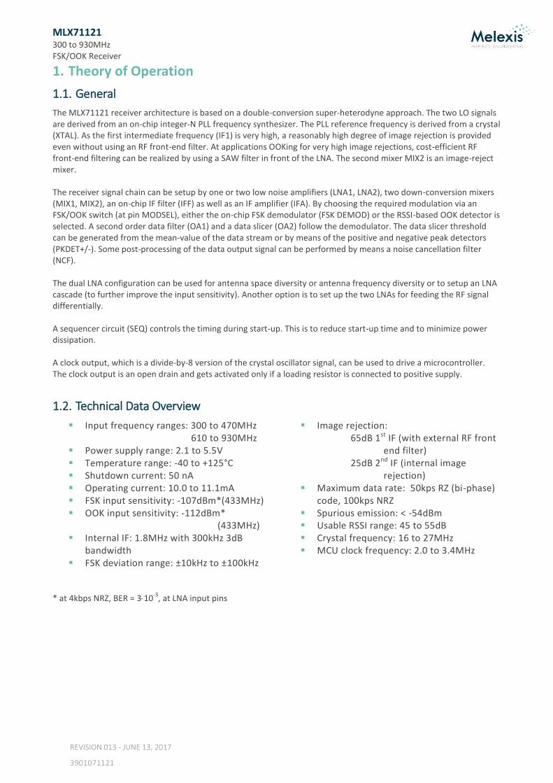
1. Theory of Operation
1.1. General
The MLX71121 receiver architecture is based on a double-conversion super-heterodyne approach. The two LO signals are derived from an on-chip integer-N PLL frequency synthesizer. The PLL reference frequency is derived from a crystal (XTAL). As the first intermediate frequency (IF1) is very high, a reasonably high degree of image rejection is provided even without using an RF front-end filter. At applications OOKing for very high image rejections, cost-efficient RF front-end filtering can be realized by using a SAW filter in front of the LNA. The second mixer MIX2 is an image-reject mixer. The receiver signal chain can be setup by one or two low noise amplifiers (LNA1, LNA2), two down-conversion mixers (MIX1, MIX2), an on-chip IF filter (IFF) as well as an IF amplifier (IFA). By choosing the required modulation via an FSK/OOK switch (at pin MODSEL), either the on-chip FSK demodulator (FSK DEMOD) or the RSSI-based OOK detector is selected. A second order data filter (OA1) and a data slicer (OA2) follow the demodulator. The data slicer threshold can be generated from the mean-value of the data stream or by means of the positive and negative peak detectors (PKDET+/-). Some post-processing of the data output signal can be performed by means a noise cancellation filter (NCF). The dual LNA configuration can be used for antenna space diversity or antenna frequency diversity or to setup an LNA cascade (to further improve the input sensitivity). Another option is to set up the two LNAs for feeding the RF signal differentially. A sequencer circuit (SEQ) controls the timing during start-up. This is to reduce start-up time and to minimize power dissipation. A clock output, which is a divide-by-8 version of the crystal oscillator signal, can be used to drive a microcontroller. The clock output is an open drain and gets activated only if a loading resistor is connected to positive supply.
1.2. Technical Data Overview
Input frequency ranges: 300 to 470MHz 610 to 930MHz
Power supply range: 2.1 to 5.5V Temperature range: -40 to +125°C Shutdown current: 50 nA Operating current: 10.0 to 11.1mA FSK input sensitivity: -107dBm*(433MHz) OOK input sensitivity: -112dBm*
(433MHz) Internal IF: 1.8MHz with 300kHz 3dB
bandwidth FSK deviation range: ±10kHz to ±100kHz
Image rejection: 65dB 1st IF (with external RF front end filter) 25dB 2nd IF (internal image rejection)
Maximum data rate: 50kps RZ (bi-phase) code, 100kps NRZ
Spurious emission: < -54dBm Usable RSSI range: 45 to 55dB Crystal frequency: 16 to 27MHz MCU clock frequency: 2.0 to 3.4MHz
* at 4kbps NRZ, BER = 310-3
, at LNA input pins
MLX71121 300 to 930MHz FSK/OOK Receiver
REVISION 013 - JUNE 13, 2017
3901071121
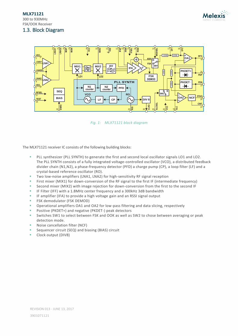
1.3. Block Diagram
Fig. 1: MLX71121 block diagram
The MLX71121 receiver IC consists of the following building blocks:
PLL synthesizer (PLL SYNTH) to generate the first and second local oscillator signals LO1 and LO2. The PLL SYNTH consists of a fully integrated voltage-controlled oscillator (VCO), a distributed feedback divider chain (N1,N2), a phase-frequency detector (PFD) a charge pump (CP), a loop filter (LF) and a crystal-based reference oscillator (RO).
Two low-noise amplifiers (LNA1, LNA2) for high-sensitivity RF signal reception First mixer (MIX1) for down-conversion of the RF signal to the first IF (intermediate frequency) Second mixer (MIX2) with image rejection for down-conversion from the first to the second IF IF Filter (IFF) with a 1.8MHz center frequency and a 300kHz 3dB bandwidth IF amplifier (IFA) to provide a high voltage gain and an RSSI signal output FSK demodulator (FSK DEMOD) Operational amplifiers OA1 and OA2 for low-pass filtering and data slicing, respectively Positive (PKDET+) and negative (PKDET-) peak detectors Switches SW1 to select between FSK and OOK as well as SW2 to chose between averaging or peak
detection mode. Noise cancellation filter (NCF) Sequencer circuit (SEQ) and biasing (BIAS) circuit Clock output (DIV8)
LNAI1
LNAI2
LNASEL
VC
C
MIX1
MIX
N
MIX
P
IFA
LO2LO1
LNA2
MIX
O
LNA1
SL
CS
EL
RO
I
CL
KO
DF
1
IFF
ROVCO
N2counter
N1counter PFD
LF CP DIV 8
FSKDEMOD
MO
DS
EL
PKDET+
PKDET_
25
463
VEE
2
VEE
7
1
LN
AO
2
LN
AO
1
28
5
8
30
32
TEST
26
RFSEL31
15
14
RS
SI
24
IFS
EL271312
VE
E11109
DF
2
OA1
1617
BIAS
SEQ
EN
RX
NCFOA2
VC
C
22 SL
C
19
ASK
FSKSW1
SW2
100k
100k
100
k
100k
100k
DTAO
29
CINT
23
DFO
PDP
PDN
18
20
21
MIX2
MLX71121 300 to 930MHz FSK/OOK Receiver
REVISION 013 - JUNE 13, 2017
3901071121
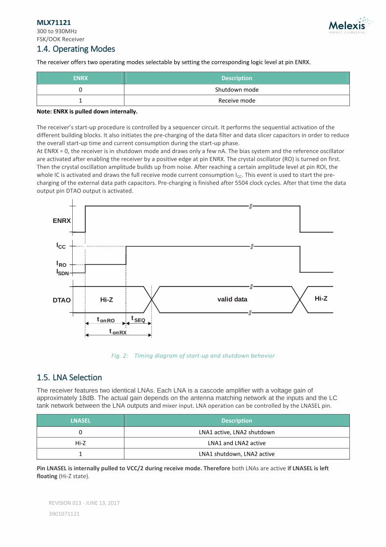
1.4. Operating Modes
The receiver offers two operating modes selectable by setting the corresponding logic level at pin ENRX.
ENRX Description
0 Shutdown mode
1 Receive mode
Note: ENRX is pulled down internally. The receiver’s start-up procedure is controlled by a sequencer circuit. It performs the sequential activation of the different building blocks. It also initiates the pre-charging of the data filter and data slicer capacitors in order to reduce the overall start-up time and current consumption during the start-up phase. At ENRX = 0, the receiver is in shutdown mode and draws only a few nA. The bias system and the reference oscillator are activated after enabling the receiver by a positive edge at pin ENRX. The crystal oscillator (RO) is turned on first. Then the crystal oscillation amplitude builds up from noise. After reaching a certain amplitude level at pin ROI, the whole IC is activated and draws the full receive mode current consumption ICC. This event is used to start the pre-charging of the external data path capacitors. Pre-charging is finished after 5504 clock cycles. After that time the data output pin DTAO output is activated.
Fig. 2: Timing diagram of start-up and shutdown behavior
1.5. LNA Selection
The receiver features two identical LNAs. Each LNA is a cascode amplifier with a voltage gain of approximately 18dB. The actual gain depends on the antenna matching network at the inputs and the LC
tank network between the LNA outputs and mixer input. LNA operation can be controlled by the LNASEL pin.
LNASEL Description
0 LNA1 active, LNA2 shutdown
Hi-Z LNA1 and LNA2 active
1 LNA1 shutdown, LNA2 active
Pin LNASEL is internally pulled to VCC/2 during receive mode. Therefore both LNAs are active if LNASEL is left floating (Hi-Z state).
valid dataHi-Z Hi-Z
ENRX
DTAO
CCI
SDNIROI
t onRO
t on RX
t SEQ
MLX71121 300 to 930MHz FSK/OOK Receiver
REVISION 013 - JUNE 13, 2017
3901071121
gain/dB
0
fcent f IF2
-40
-20
B40dB
B3dB
1.6. Mixer Section
The mixer section consists of two mixers. Both are double-balanced mixers. The second mixer is built as an image rejection mixer. The first mixer’s inputs (MIXP and MIXN) are functionally the same. For single-ended drive, the unused input has to be tied to ground via a capacitor. A soft band-pass filter is placed between the mixers.
RFSEL Description
0 Input frequency range 300 to 470MHz
1 Input frequency range 610 to 930MHz
Pin RFSEL is used to select the required RF band. The LO frequencies and the proper sidebands for image suppression will be set accordingly.
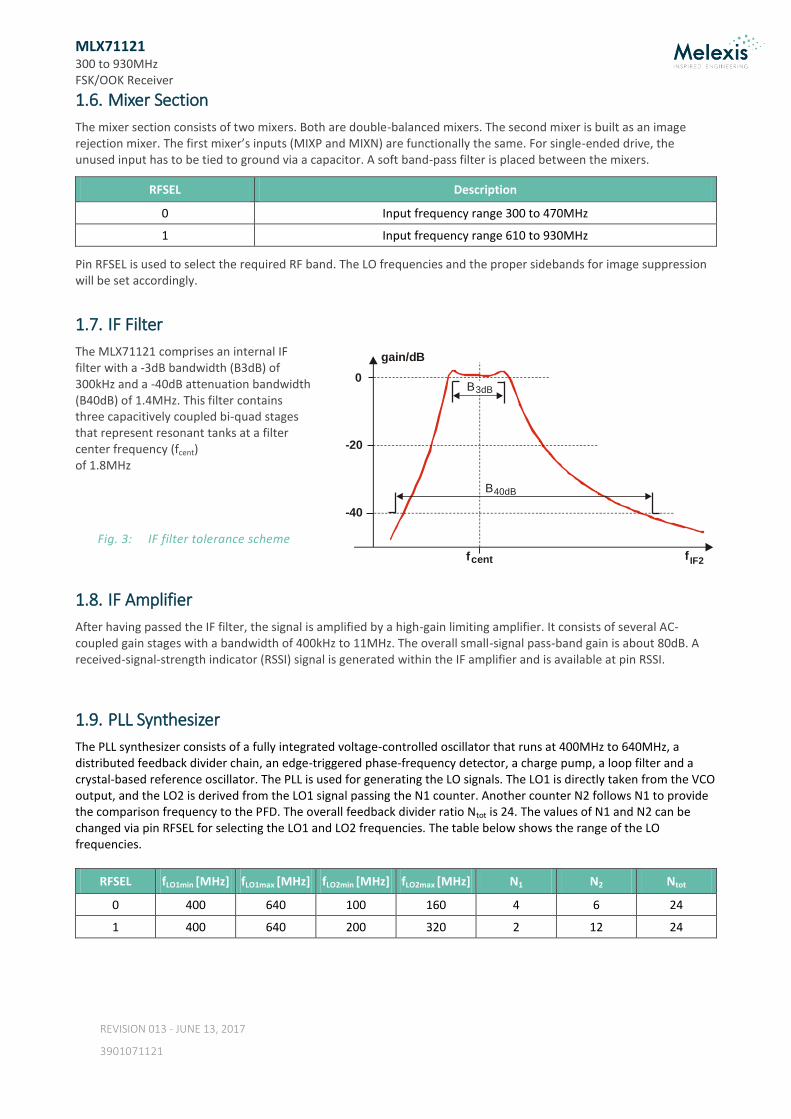
1.7. IF Filter
The MLX71121 comprises an internal IF filter with a -3dB bandwidth (B3dB) of 300kHz and a -40dB attenuation bandwidth (B40dB) of 1.4MHz. This filter contains three capacitively coupled bi-quad stages that represent resonant tanks at a filter center frequency (fcent) of 1.8MHz
Fig. 3: IF filter tolerance scheme
1.8. IF Amplifier
After having passed the IF filter, the signal is amplified by a high-gain limiting amplifier. It consists of several AC-coupled gain stages with a bandwidth of 400kHz to 11MHz. The overall small-signal pass-band gain is about 80dB. A received-signal-strength indicator (RSSI) signal is generated within the IF amplifier and is available at pin RSSI.
1.9. PLL Synthesizer
The PLL synthesizer consists of a fully integrated voltage-controlled oscillator that runs at 400MHz to 640MHz, a distributed feedback divider chain, an edge-triggered phase-frequency detector, a charge pump, a loop filter and a crystal-based reference oscillator. The PLL is used for generating the LO signals. The LO1 is directly taken from the VCO output, and the LO2 is derived from the LO1 signal passing the N1 counter. Another counter N2 follows N1 to provide the comparison frequency to the PFD. The overall feedback divider ratio Ntot is 24. The values of N1 and N2 can be changed via pin RFSEL for selecting the LO1 and LO2 frequencies. The table below shows the range of the LO frequencies.
RFSEL fLO1min [MHz] fLO1max [MHz] fLO2min [MHz] fLO2max [MHz] N1 N2 Ntot
0 400 640 100 160 4 6 24
1 400 640 200 320 2 12 24
MLX71121 300 to 930MHz FSK/OOK Receiver
REVISION 013 - JUNE 13, 2017
3901071121
1.10. Reference Oscillator
A Colpitts crystal oscillator with integrated functional capacitors is used as the reference oscillator (RO) of the PLL synthesizer. The equivalent input capacitance CRO offered to the crystal at pin ROI is about 18pF. The crystal oscillator features an amplitude control loop. This is to assure a very stable frequency over the specified supply voltage and temperature range together with a short start-up time. A buffer amplifier with hysteresis is between RO and PFD. Also a clock divider follows the buffer.
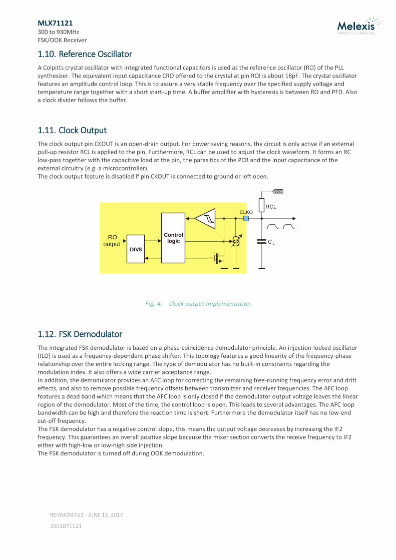
1.11. Clock Output
The clock output pin CKOUT is an open-drain output. For power saving reasons, the circuit is only active if an external pull-up resistor RCL is applied to the pin. Furthermore, RCL can be used to adjust the clock waveform. It forms an RC low-pass together with the capacitive load at the pin, the parasitics of the PCB and the input capacitance of the external circuitry (e.g. a microcontroller). The clock output feature is disabled if pin CKOUT is connected to ground or left open.
Fig. 4: Clock output implementation
1.12. FSK Demodulator
The integrated FSK demodulator is based on a phase-coincidence demodulator principle. An injection-locked oscillator (ILO) is used as a frequency-dependent phase shifter. This topology features a good linearity of the frequency-phase relationship over the entire locking range. The type of demodulator has no built-in constraints regarding the modulation index. It also offers a wide carrier acceptance range. In addition, the demodulator provides an AFC loop for correcting the remaining free-running frequency error and drift effects, and also to remove possible frequency offsets between transmitter and receiver frequencies. The AFC loop features a dead band which means that the AFC loop is only closed if the demodulator output voltage leaves the linear region of the demodulator. Most of the time, the control loop is open. This leads to several advantages. The AFC loop bandwidth can be high and therefore the reaction time is short. Furthermore the demodulator itself has no low-end cut-off frequency. The FSK demodulator has a negative control slope, this means the output voltage decreases by increasing the IF2 frequency. This guarantees an overall positive slope because the mixer section converts the receive frequency to IF2 either with high-low or low-high side injection. The FSK demodulator is turned off during OOK demodulation.
CLKO
DIV8
Controllogic
RO output
RCL
CL
VCC
MLX71121 300 to 930MHz FSK/OOK Receiver
REVISION 013 - JUNE 13, 2017
3901071121
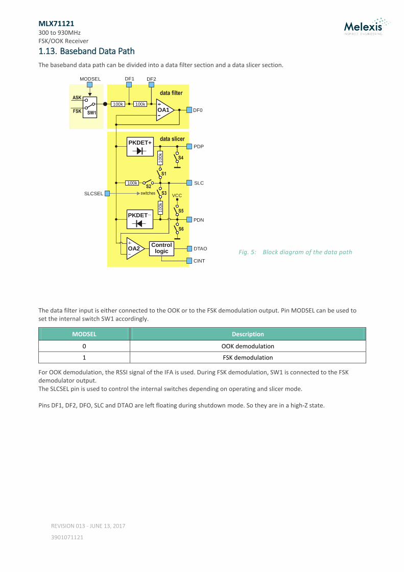
1.13. Baseband Data Path
The baseband data path can be divided into a data filter section and a data slicer section.
Fig. 5: Block diagram of the data path
The data filter input is either connected to the OOK or to the FSK demodulation output. Pin MODSEL can be used to set the internal switch SW1 accordingly.
MODSEL Description
0 OOK demodulation
1 FSK demodulation
For OOK demodulation, the RSSI signal of the IFA is used. During FSK demodulation, SW1 is connected to the FSK demodulator output. The SLCSEL pin is used to control the internal switches depending on operating and slicer mode. Pins DF1, DF2, DFO, SLC and DTAO are left floating during shutdown mode. So they are in a high-Z state.
PKDET+
PKDET_
OA1
OA2
data filter
data slicer
DF1 DF2
DF0
Controllogic
DTAO
CINT
PDP
SLC
MODSEL
ASK
FSK SW1
100k 100k
100
k
S1
100kS2
10
0k
S3
S4
VCC
PDN
S5
S6
SLCSEL switches
MLX71121 300 to 930MHz FSK/OOK Receiver
REVISION 013 - JUNE 13, 2017
3901071121
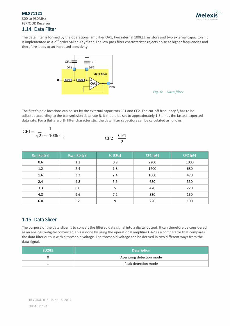
1.14. Data Filter
The data filter is formed by the operational amplifier OA1, two internal 100k resistors and two external capacitors. It is implemented as a 2
nd order Sallen-Key filter. The low pass filter characteristic rejects noise at higher frequencies and
therefore leads to an increased sensitivity.
Fig. 6: Data filter
The filter’s pole locations can be set by the external capacitors CF1 and CF2. The cut-off frequency fc has to be adjusted according to the transmission data rate R. It should be set to approximately 1.5 times the fastest expected data rate. For a Butterworth filter characteristic, the data filter capacitors can be calculated as follows.
cf100kπ2
1CF1
2
CF1CF2
RRZ [kbit/s] RNRZ [kbit/s] fc [kHz] CF1 [pF] CF2 [pF]
0.6 1.2 0.9 2200 1000
1.2 2.4 1.8 1200 680
1.6 3.2 2.4 1000 470
2.4 4.8 3.6 680 330
3.3 6.6 5 470 220
4.8 9.6 7.2 330 150
6.0 12 9 220 100
1.15. Data Slicer
The purpose of the data slicer is to convert the filtered data signal into a digital output. It can therefore be considered as an analog-to-digital converter. This is done by using the operational amplifier OA2 as a comparator that compares the data filter output with a threshold voltage. The threshold voltage can be derived in two different ways from the data signal.
SLCSEL Description
0 Averaging detection mode
1 Peak detection mode
OA1
data filter
DF1 DF2
DF0
100k 100k
CF1 CF2

MLX71121 300 to 930MHz FSK/OOK Receiver
REVISION 013 - JUNE 13, 2017
3901071121
1.15.1. Averaging Detection Mode
The simplest configuration is the averaging or RC integration
method. Here an on-chip 100k resistor together with an external slicer capacitor (CSL) are forming an RC low-pass filter. This way the threshold voltage automatically adjusts to the mean or average value of the analog input voltage. To create a stable threshold voltage, the cut-off frequency of the low pass has to be lower than the lowest signal frequency.
100k
τCSL AVG
RZ
AVGR
1.5τ
A long string of zeros or ones, like in NRZ codes, can cause a drift of the threshold. That’s why a Manchester or other DC-free coding scheme works best. The peak detectors are disabled during averaging detection mode, and the output pins PDP and PDN are pulled to ground (S4, S6 are closed).
Fig. 7: Data path in averaging detection mode
1.15.2. Peak Detection Mode
Peak detection mode has a general advantage over averaging detection mode because of the part attack and slow release times. Peak detection should be used for all non-DC-free codes like NRZ. In this configuration the threshold is generated by using the positive and negative peak detectors. The slicer comparator threshold is set to the midpoint between the high output and the low output of the data filter by an on-chip resistance divider. Two external capacitors (CP1, CP2) determine the release times for the positive and negative envelope. The two on-chip resistors provide a path for the capacitors to discharge. This allows the peak detectors to dynamically follow peak changes of the data filter output voltage. The attack times are very short due to the high peak detector load currents of about 500uA. The decay time constant mainly depends on the longest time period without bit polarity change. This corresponds to the maximum number of consecutive bits with the same polarity (NMAX).
100k
τCP1/2 DECAY
NRZ
MAXDECAY
R
Nτ
Fig. 8: Data path in peak detection mode
If the receiver is in shutdown mode and peak detection mode is selected then the peak detectors are disabled and the output of the positive peak detector (PDP) is connected to VEE (S4 is closed) and the output of the negative peak detector (PDN) is connected to VCC (S5 is closed). This guarantees the correct biasing of CP1 and CP2 during start-up.
CSL
PKDET+
PKDET_
OA2
data slicer
PDP
SLC
10
0k
S1
100kS2
100
k
S3
S4
Controllogic
DTAO
CINT
VCC
PDN
S5
S6
data filter
SLCSEL switches
VC
C
CP1
CP2
PKDET+
PKDET_
OA2
data slicerPDP
PDN
SLC
10
0k
S1
100kS2
100
k
S3
S4
VCC
S5
S6
Controllogic
DTAO
CINT
data filter
SLCSEL switches

MLX71121 300 to 930MHz FSK/OOK Receiver
REVISION 013 - JUNE 13, 2017
3901071121
1.16. Data Output and Noise Cancellation Filter
The data output pin DTAO delivers the demodulated data signal which can be further processed by a noise cancellation filter (NCF). The NCF can be disabled if pin CINT is connected to ground. In this case the multiplexer (MUX) connects the receiver output DTAO directly to the data slicer output.
Fig. 9: Data output and noise filter
The noise cancellation filter can suppress random pulses in the data output which are shorter than tmin.
RZNRZ RRt
66
min
6- 105.710151015CF3
The NCF can also operate as a muting circuit. So if the RF input signal is below sensitivity level (or if no RF signal is applied) then the data output will go to a constant DC level (either HIGH or LOW). This can be achieved by setting the bandwidth of the preceding data filter (sec 1.13) about 10 times higher than the bandwidth of the NCF. Further the data filter cutoff frequency must be higher than the data rate, so the noise pulses are shorter than the shortest data pulse. Otherwise, the NCF will not be able to distinguish between noise and data pulses. Having the NCF activated is a good means for reducing the computing power of the microcontroller that follows the receiver IC for further data processing. In contrast to a conventional muting (or squelch) circuit, this topology does not need the RSSI signal for level indication. The filtering process is done by means of an analogue integrator. The cut-off frequency of the NCF is set by the external capacitor connected to pin CINT. This capacitor CF3 should be set according to the maximum data rate. Below table provides some recommendations.. During receiver start-up a sequencer checks if pin CINT is connected to a capacitor or to ground. The maximum value of CF3 should not exceed 12nF. This defines the lowest data rate that can be processed if the noise cancellation filter is activated.
RRZ [kbit/s] RNRZ [kbit/s] CF3[nF]
0.6 1.2 12
1.2 2.4 6.8
1.6 3.2 4.7
2.4 4.8 3.3
3.3 6.6 2.2
4.8 9.6 1.5
6.0 12 1.2
In shutdown mode pin DTAO is set to Hi-Z state.
CF3
data sliceroutput
CINTNCF
noise cancellation filter
MUX
DTAO
MLX71121 300 to 930MHz FSK/OOK Receiver
REVISION 013 - JUNE 13, 2017
3901071121
2. Functional Description
2.1. Frequency Planning
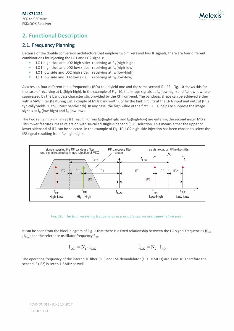
Because of the double conversion architecture that employs two mixers and two IF signals, there are four different combinations for injecting the LO1 and LO2 signals:
LO1 high side and LO2 high side: receiving at fRF(high-high) LO1 high side and LO2 low side: receiving at fRF(high-low) LO1 low side and LO2 high side: receiving at fRF(low-high) LO1 low side and LO2 low side: receiving at fRF(low-low)
As a result, four different radio frequencies (RFs) could yield one and the same second IF (IF2). Fig. 10 shows this for the case of receiving at fRF(high-high). In the example of Fig. 10, the image signals at fRF(low-high) and fRF(low-low) are suppressed by the bandpass characteristic provided by the RF front-end. The bandpass shape can be achieved either with a SAW filter (featuring just a couple of MHz bandwidth), or by the tank circuits at the LNA input and output (this typically yields 30 to 60MHz bandwidth). In any case, the high value of the first IF (IF1) helps to suppress the image signals at fRF(low-high) and fRF(low-low).
The two remaining signals at IF1 resulting from fRF(high-high) and fRF(high-low) are entering the second mixer MIX2. This mixer features image rejection with so-called single-sideband (SSB) selection. This means either the upper or lower sideband of IF1 can be selected. In the example of Fig. 10, LO2 high-side injection has been chosen to select the IF2 signal resulting from fRF(high-high).
Fig. 10: The four receiving frequencies in a double conversion superhet receiver
It can be seen from the block diagram of Fig. 1 that there is a fixed relationship between the LO signal frequencies (fLO1 , fLO2) and the reference oscillator frequency fRO.
LO21LO1 fNf RO2LO2 fNf
The operating frequency of the internal IF filter (IFF) and FSK demodulator (FSK DEMOD) are 1.8MHz. Therefore the second IF (IF2) is set to 1.8MHz as well.
fLO2 fLO2
fLO1fRFfRF
fRFfRF
MLX71121 300 to 930MHz FSK/OOK Receiver
REVISION 013 - JUNE 13, 2017
3901071121
2.2. Calculation of Frequency Settings
The receiver has two predefined receive frequency plans which can be selected by the RFSEL control pin. Depending on the logic level of RFSEL pin the sideband selection of the second mixer and the counter settings for N1 and N2 are changed accordingly.
RFSEL Injection fRFmin [MHz] fRFmax [MHz] N1 N2
0 high-low 300 470 4 6
1 low-high 610 930 2 12
The following table shows the relationships of several internal receiver frequencies for the two input frequency ranges.
fRF [MHz] fIF1 fLO1 fLO2 fRO
300 to 470
1N
fNf
1
IF21RF
1N
)f(fN
1
IF2RF1
1N
ff
1
IF2RF
1)(NN
ff
12
IF2RF
610 to 930
1N
fNf
1
IF21RF
1N
)f(fN
1
IF2RF1
1N
ff
1
IF2RF
1)(NN
ff
12
IF2RF
Given IF2 = 1.8MHz and the corresponding N1, N2 counter settings, above equations can be transferred into the following table.
fRF [MHz] fIF1 fLO1 fLO2 fRO
300 to 470
3
7.2MHzfRF
3
)1.8MHz4(fRF
3
1.8MHzfRF
18
1.8MHzfRF
610 to 930
3
3.6MHzfRF
3
)1.8MHz2(fRF
36
1.8MHzfRF
MLX71121 300 to 930MHz FSK/OOK Receiver
REVISION 013 - JUNE 13, 2017
3901071121
2.3. Standard Frequency Plans
IF2 = 1.8MHz
RFSEL fRF [MHz] fIF1 [MHz] fLO1 [MHz] fLO2 [MHz] fRO [MHz]
0 315 107.40 422.40 105.60 17.600000
433.92 147.04 580.96 145.24 24.206667
1 868.3 288.23 580.07 290.03 24.169444
915 303.80 611.20 305.60 25.466667
2.4. 433/868MHz Frequency Diversity
The receiver’s multi-band functionality can be used to operate at two different frequency bands just by changing the logic level at pin RFSEL and without changing the crystal. This feature is applicable for common use of the 433 and 868MHz bands. Below table shows the corresponding frequency plans.
IF2 = 1.8MHz
RFSEL fRF [MHz] fIF1 [MHz] fLO1 [MHz] fLO2 [MHz] fRO [MHz]
0 433.25 146.82 580.07 145.02 24.169444
1 868.3 288.23 580.07 290.03

MLX71121 300 to 930MHz FSK/OOK Receiver
REVISION 013 - JUNE 13, 2017
3901071121
3. Pin Definitions and Descriptions
Pin No. Name I/O Type Functional Schematic Description
3 LNAO1 analog output
LNA output 1
1 LNAI1 analog input
LNA input 1
2 VEE ground negative supply voltage
4 MIXP analog input
MIX1 positive input
5 MIXN analog input
MIX1 negative input
6 LNAO2 analog output
LNA output 2
8 LNAI2 analog input
LNA input 2
7 VEE ground negative supply voltage
9 VCC supply positive supply voltage
10 MIXO analog output
not used pin left open
mixer 2 output
11 VEE ground negative supply voltage
12 IFAP analog input not used
pins left open
IF amplifier positive input
13 IFAN analog input
IF amplifier negative input
14 MODSEL CMOS input
modulation select input
Vbias
Vbias
VEE
VEE
VCC
1
3
LNAO1
LNAI1
1k
MIXP
4
VEE VEE
VCC VCC
5
MIXN
Vbias
2k
2k
Vbias
Vbias
VEE
VEE
VCC
8
6
LNAO2
LNAI2
1k
VEE VEE
VCC VCC
14
MODSEL400

MLX71121 300 to 930MHz FSK/OOK Receiver
REVISION 013 - JUNE 13, 2017
3901071121
Pin No. Name I/O Type Functional Schematic Description
15 SLCSEL CMOS input
slicer mode select input
16 DF2 analog I/O
data filter connection 2
17 DF1 analog I/O
data filter connection 1
18 DFO analog output
data filter output
19 SLC analog input
slicer reference input
20 PDP analog output
peak detector positive output
21 PDN analog output
peak detector negative output
VEE VEE
VCC VCC
15
SLCSEL400
VCC
VEE
VCC
DF2
16
400
VEE
DF1
17
400
100
k
100
k
VCC
VEE
VCC VCC
18
DFO400
VEE
VCC
19
SLC400 100k
10
0k
100
k
VEE
VCC VCC
20
PDP400
VEE
VCC
21
PDN400
MLX71121 300 to 930MHz FSK/OOK Receiver
REVISION 013 - JUNE 13, 2017
3901071121
Pin No. Name I/O Type Functional Schematic Description
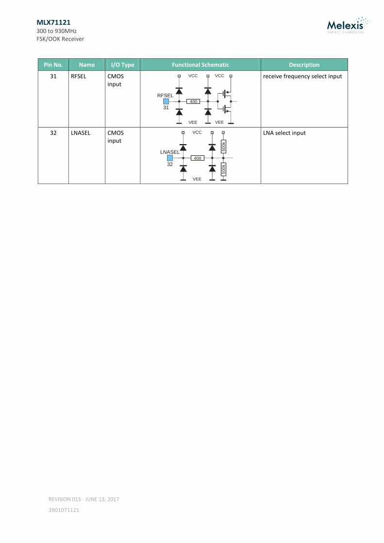
22 VCC supply positive supply voltage
23 CINT analog input
capacitor for noise cancellation filter
pin must be connected to ground if noise cancellation filter is not used
24 RSSI analog output
receive signal strength indication
25 ROI analog input
reference oscillator input
26 TEST CMOS input
not used connect to ground
test pin
27 IFSEL CMOS input
not used connect pin to ground
IF select input
28 CLKO CMOS output
clock output
connect pull-up resistor to activate clock
29 DTAO CMOS output
data output
30 ENRX CMOS input
enable RX mode control
VEE
VCC
23
CINT
51k
VEE VEE
VCC
24
RSSI400
25
ROI
VEE VEE
VCCVCC1
6k
VEE
VCC
28
CLKO
VEE
VCC VCC
29
DTAO220
380
k
VEE VEE
VCC VCC
30
ENRX400
MLX71121 300 to 930MHz FSK/OOK Receiver
REVISION 013 - JUNE 13, 2017
3901071121
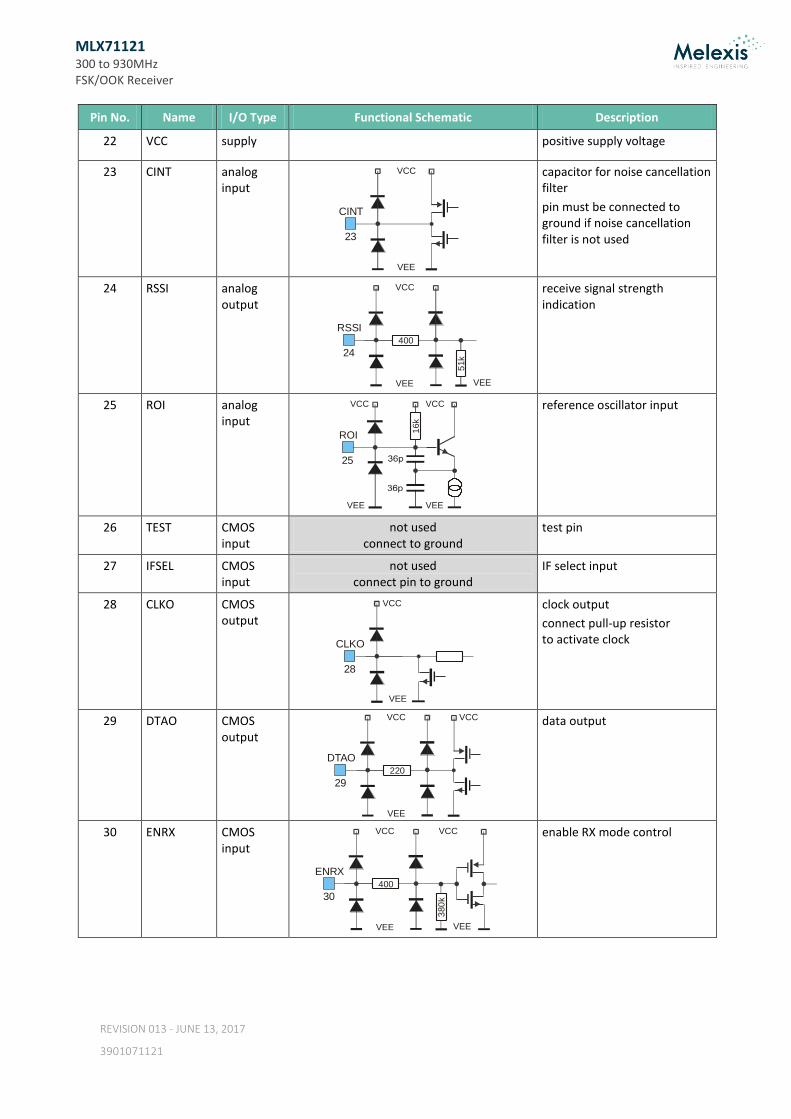
Pin No. Name I/O Type Functional Schematic Description
31 RFSEL CMOS input
receive frequency select input
32 LNASEL CMOS input
LNA select input
VEE VEE
VCC VCC
31
RFSEL400
VEE
VCC
32
LNASEL400
500
k50
0k
MLX71121 300 to 930MHz FSK/OOK Receiver
REVISION 013 - JUNE 13, 2017
3901071121
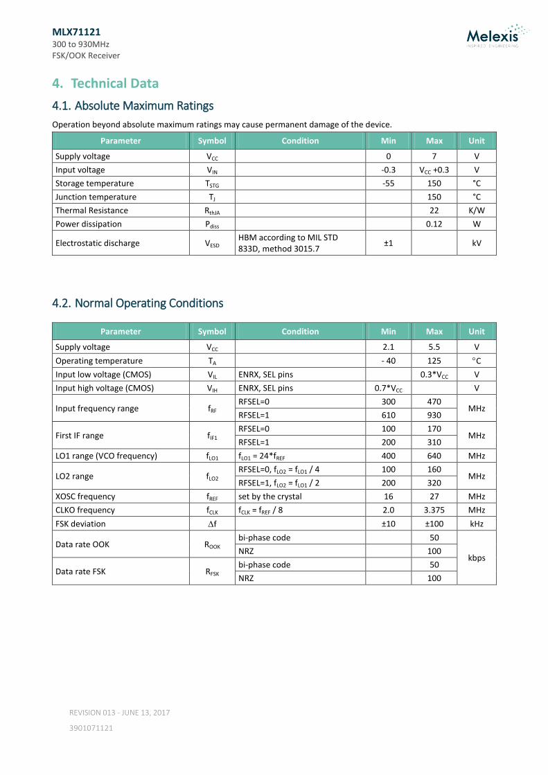
4. Technical Data
4.1. Absolute Maximum Ratings
Operation beyond absolute maximum ratings may cause permanent damage of the device.
Parameter Symbol Condition Min Max Unit
Supply voltage VCC 0 7 V
Input voltage VIN -0.3 VCC +0.3 V
Storage temperature TSTG -55 150 °C
Junction temperature TJ 150 °C
Thermal Resistance RthJA 22 K/W
Power dissipation Pdiss 0.12 W
Electrostatic discharge VESD HBM according to MIL STD 833D, method 3015.7
±1 kV
4.2. Normal Operating Conditions
Parameter Symbol Condition Min Max Unit
Supply voltage VCC 2.1 5.5 V
Operating temperature TA - 40 125 C
Input low voltage (CMOS) VIL ENRX, SEL pins 0.3*VCC V
Input high voltage (CMOS) VIH ENRX, SEL pins 0.7*VCC V
Input frequency range fRF RFSEL=0 300 470
MHz RFSEL=1 610 930
First IF range fIF1 RFSEL=0 100 170
MHz RFSEL=1 200 310
LO1 range (VCO frequency) fLO1 fLO1 = 24*fREF 400 640 MHz
LO2 range fLO2 RFSEL=0, fLO2 = fLO1 / 4 100 160
MHz RFSEL=1, fLO2 = fLO1 / 2 200 320
XOSC frequency fREF set by the crystal 16 27 MHz
CLKO frequency fCLK fCLK = fREF / 8 2.0 3.375 MHz
FSK deviation f ±10 ±100 kHz
Data rate OOK ROOK bi-phase code 50
kbps NRZ 100
Data rate FSK RFSK bi-phase code 50
NRZ 100
MLX71121 300 to 930MHz FSK/OOK Receiver
REVISION 013 - JUNE 13, 2017
3901071121
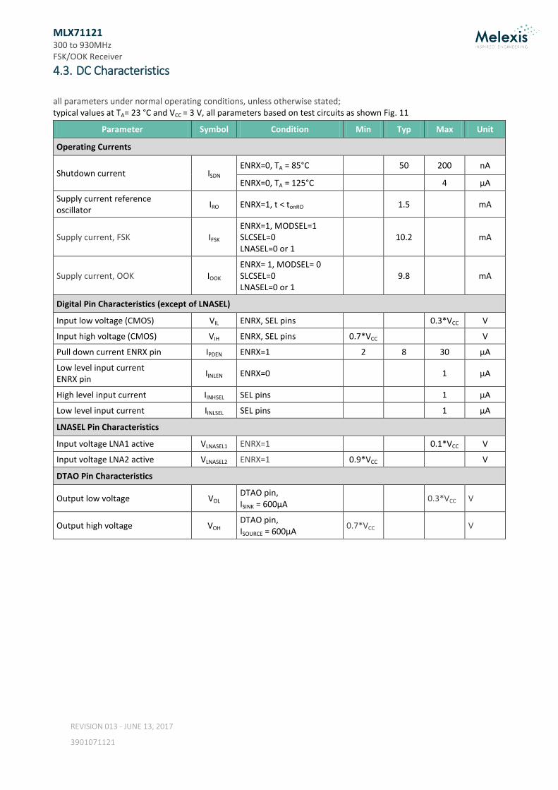
4.3. DC Characteristics
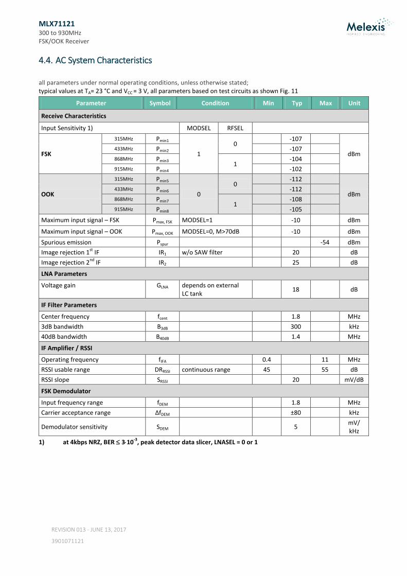
all parameters under normal operating conditions, unless otherwise stated; typical values at TA= 23 °C and VCC = 3 V, all parameters based on test circuits as shown Fig. 11
Parameter Symbol Condition Min Typ Max Unit
Operating Currents
Shutdown current ISDN ENRX=0, TA = 85°C 50 200 nA
ENRX=0, TA = 125°C 4 µA
Supply current reference oscillator
IRO ENRX=1, t < tonRO 1.5 mA
Supply current, FSK IFSK ENRX=1, MODSEL=1 SLCSEL=0 LNASEL=0 or 1
10.2 mA
Supply current, OOK IOOK ENRX= 1, MODSEL= 0 SLCSEL=0 LNASEL=0 or 1
9.8 mA
Digital Pin Characteristics (except of LNASEL)
Input low voltage (CMOS) VIL ENRX, SEL pins 0.3*VCC V
Input high voltage (CMOS) VIH ENRX, SEL pins 0.7*VCC V
Pull down current ENRX pin IPDEN ENRX=1 2 8 30 µA
Low level input current ENRX pin
IINLEN ENRX=0 1 µA
High level input current IINHSEL SEL pins 1 µA
Low level input current IINLSEL SEL pins 1 µA
LNASEL Pin Characteristics
Input voltage LNA1 active VLNASEL1 ENRX=1 0.1*VCC V
Input voltage LNA2 active VLNASEL2 ENRX=1 0.9*VCC V
DTAO Pin Characteristics
Output low voltage VOL DTAO pin, ISINK = 600µA
0.3*VCC V
Output high voltage VOH DTAO pin, ISOURCE = 600µA
0.7*VCC V
MLX71121 300 to 930MHz FSK/OOK Receiver
REVISION 013 - JUNE 13, 2017
3901071121
4.4. AC System Characteristics
all parameters under normal operating conditions, unless otherwise stated; typical values at TA= 23 °C and VCC = 3 V, all parameters based on test circuits as shown Fig. 11
Parameter Symbol Condition Min Typ Max Unit
Receive Characteristics
Input Sensitivity 1) MODSEL RFSEL
FSK
315MHz Pmin1
1
0 -107
dBm 433MHz Pmin2 -107
868MHz Pmin3 1
-104
915MHz Pmin4 -102
OOK
315MHz Pmin5
0
0 -112
dBm 433MHz Pmin6 -112
868MHz Pmin7 1
-108
915MHz Pmin8 -105
Maximum input signal – FSK Pmax, FSK MODSEL=1 -10 dBm
Maximum input signal – OOK Pmax, OOK MODSEL=0, M>70dB -10 dBm
Spurious emission Pspur -54 dBm
Image rejection 1st
IF IR1 w/o SAW filter 20 dB
Image rejection 2nd
IF IR2 25 dB
LNA Parameters
Voltage gain GLNA depends on external LC tank
18 dB
IF Filter Parameters
Center frequency fcent 1.8 MHz
3dB bandwidth B3dB 300 kHz
40dB bandwidth B40dB 1.4 MHz
IF Amplifier / RSSI
Operating frequency fIFA 0.4 11 MHz
RSSI usable range DRRSSI continuous range 45 55 dB
RSSI slope SRSSI 20 mV/dB
FSK Demodulator
Input frequency range fDEM 1.8 MHz
Carrier acceptance range ΔfDEM ±80 kHz
Demodulator sensitivity SDEM 5 mV/ kHz
1) at 4kbps NRZ, BER 310-3
, peak detector data slicer, LNASEL = 0 or 1

MLX71121 300 to 930MHz FSK/OOK Receiver
REVISION 013 - JUNE 13, 2017
3901071121
Parameter Symbol Condition Min Typ Max Unit
Baseband Data Path
Data filter bandwidth BDF depending on CF1, CF2 100 kHz
Peak detector load current IPKD 500 µA
Start-up Parameters
Reference oscillator start-up time
tonRO depending on crystal parameters
350 650 µs
Sequencer time tSEQ 5504 / fREF 200 250 350 µs
Receiver start-up time tonRX tonRO + tSEQ 0.6 1 ms
Frequency Stability
Frequency pulling by supply voltage dfVCC ±3 ppm/V
4.5. External Components
Parameter Symbol Condition Min Max Unit
Crystal Parameters
Crystal frequency f0 fundamental mode, AT 16 27 MHz
Load capacitance CL 10 15 pF
Static capacitance C0 5 pF
Series resistance R1 60
Noise Cancellation Filter
Integrator capacitor CF3 depends on data rate 12 nF
Clock Output
Pull-up resistor RCL 600
Load capacitance CL 50 pF
MLX71121 300 to 930MHz FSK/OOK Receiver
REVISION 013 - JUNE 13, 2017
3901071121
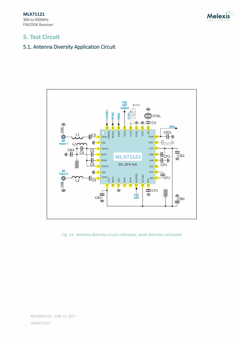
5. Test Circuit
5.1. Antenna Diversity Application Circuit
Fig. 11: Antenna diversity circuit schematic, peak detectors activated
VC
C
CB0
CB2
VC
C
CB3
LN
AS
EL
RF
SE
L
EN
RX
MLX71121
17
18
19
20
21
22
23
24
9 10 11 12 13 14 15 16
8
1
2
3
4
5
6
7
32L QFN 5x5
VC
C
RF
SE
L
VE
E
IFA
P
IFA
N
MO
DS
EL
SL
CS
EL
DF
2
RSSI
DFO
DF1
DTA
O
SLC
PDP
VCC
VCC
PDN
MIXN
MIXP
LNAI1 CL
KO
TE
ST
RO
I
IFS
EL
LNAO2
LNAO1
LNAI2
MIX
O
VEE
VEE
32
30
29
28
27
2531
26
EN
RX
CINT
FSKASK
output
FSKASK
50
C9L3
50
C3
C4C5
C6
L1
L2
CF1
CF2
CP1
CP2
RSSI
CB1
CX
XTAL
CRS
CL
KO
CF3
RC
L
MLX71121 300 to 930MHz FSK/OOK Receiver
REVISION 013 - JUNE 13, 2017
3901071121
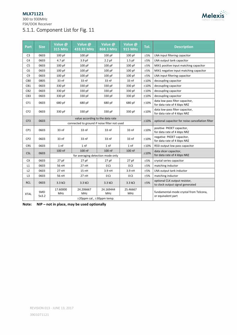
5.1.1. Component List for Fig. 11
Part Size Value @ 315 MHz
Value @ 433.92 MHz
Value @ 868.3 MHz
Value @ 915 MHz
Tol. Description
C3 0603 100 pF 100 pF 100 pF 100 pF 5% LNA input filtering capacitor
C4 0603 4.7 pF 3.9 pF 2.2 pF 1.5 pF 5% LNA output tank capacitor
C5 0603 100 pF 100 pF 100 pF 100 pF 5% MIX1 positive input matching capacitor
C6 0603 100 pF 100 pF 100 pF 100 pF 5% MIX1 negative input matching capacitor
C9 0603 100 pF 100 pF 100 pF 100 pF 5% LNA input filtering capacitor
CB0 0805 33 nF 33 nF 33 nF 33 nF 10% decoupling capacitor
CB1 0603 330 pF 330 pF 330 pF 330 pF 10% decoupling capacitor
CB2 0603 330 pF 330 pF 330 pF 330 pF 10% decoupling capacitor
CB3 0603 330 pF 330 pF 330 pF 330 pF 10% decoupling capacitor
CF1 0603 680 pF 680 pF 680 pF 680 pF 10% data low-pass filter capacitor, for data rate of 4 kbps NRZ
CF2 0603 330 pF 330 pF 330 pF 330 pF 10% data low-pass filter capacitor, for data rate of 4 kbps NRZ
CF3 0603 value according to the data rate
10% optional capacitor for noise cancellation filter connected to ground if noise filter not used
CP1 0603 33 nF 33 nF 33 nF 33 nF 10% positive PKDET capacitor, for data rate of 4 kbps NRZ
CP2 0603 33 nF 33 nF 33 nF 33 nF 10% negative PKDET capacitor, for data rate of 4 kbps NRZ
CRS 0603 1 nF 1 nF 1 nF 1 nF 10% RSSI output low pass capacitor
CSL 0603 100 nF 100 nF 100 nF 100 nF
10% data slicer capacitor, for data rate of 4 kbps NRZ for averaging detection mode only
CX 0603 27 pF 27 pF 27 pF 27 pF 5% crystal series capacitor
L1 0603 56 nH 27 nH 0 0 5% matching inductor
L2 0603 27 nH 15 nH 3.9 nH 3.9 nH 5% LNA output tank inductor
L3 0603 56 nH 27 nH 0 0 5% matching inductor
RCL 0603 3.3 k 3.3 k 3.3 k 3.3 k 5% optional CLK output resistor, to clock output signal generated
XTAL SMD 5x3.2
17.60000 MHz
24.206667 MHz
24.169444 MHz
25.46667 MHz
fundamental-mode crystal from Telcona, or equivalent part
20ppm cal., 30ppm temp.
Note: NIP – not in place, may be used optionally
MLX71121 300 to 930MHz FSK/OOK Receiver
REVISION 013 - JUNE 13, 2017
3901071121
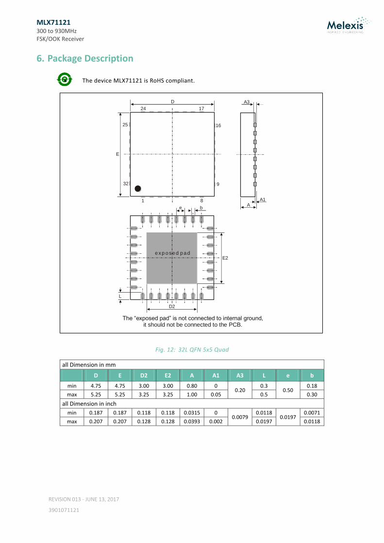
6. Package Description
The device MLX71121 is RoHS compliant.
Fig. 12: 32L QFN 5x5 Quad
all Dimension in mm
D E D2 E2 A A1 A3 L e b
min 4.75 4.75 3.00 3.00 0.80 0 0.20
0.3 0.50
0.18
max 5.25 5.25 3.25 3.25 1.00 0.05 0.5 0.30
all Dimension in inch
min 0.187 0.187 0.118 0.118 0.0315 0 0.0079
0.0118 0.0197
0.0071
max 0.207 0.207 0.128 0.128 0.0393 0.002 0.0197 0.0118
A3
AA11 8
24 17
16
932
25
D
E
e b
L
D2
E2exp osed pad
The “exposed pad” is not connected to internal ground, it should not be connected to the PCB.

MLX71121 300 to 930MHz FSK/OOK Receiver
Page 27 of 28
REVISION 013 - JUNE 13, 2017
3901071121
7. Standard Information Regarding Manufacturability of Melexis Products with Different Soldering Processes Our products are classified and qualified regarding soldering technology, solderability and moisture sensitivity level according to following test methods: Reflow Soldering SMD’s (Surface Mount Devices) IPC/JEDEC J-STD-020
Moisture/Reflow Sensitivity Classification for Nonhermetic Solid State Surface Mount Devices (classification reflow profiles according to table 5-2) EIA/JEDEC JESD22-A113
Preconditioning of Nonhermetic Surface Mount Devices Prior to Reliability Testing (reflow profiles according to table 2) Wave Soldering SMD’s (Surface Mount Devices) and THD’s (Through Hole Devices) EN60749-20
Resistance of plastic- encapsulated SMD’s to combined effect of moisture and soldering heat EIA/JEDEC JESD22-B106 and EN60749-15
Resistance to soldering temperature for through-hole mounted devices Iron Soldering THD’s (Through Hole Devices) EN60749-15
Resistance to soldering temperature for through-hole mounted devices Solderability SMD’s (Surface Mount Devices) and THD’s (Through Hole Devices) EIA/JEDEC JESD22-B102 and EN60749-21
Solderability For all soldering technologies deviating from above mentioned standard conditions (regarding peak temperature, temperature gradient, temperature profile etc) additional classification and qualification tests have to be agreed upon with Melexis. The application of Wave Soldering for SMD’s is allowed only after consulting Melexis regarding assurance of adhesive strength between device and board. Melexis recommends reviewing on our web site the General Guidelines soldering recommendation (http://www.melexis.com/Quality_soldering.aspx) as well as trim&form recommendations (http://www.melexis.com/Assets/Trim-and-form-recommendations-5565.aspx). Melexis is contributing to global environmental conservation by promoting lead free solutions. For more information on qualifications of RoHS compliant products (RoHS = European directive on the Restriction Of the use of certain Hazardous Substances) please visit the quality page on our website: http://www.melexis.com/quality.aspx
8. ESD Precautions Electronic semiconductor products are sensitive to Electro Static Discharge (ESD). Always observe Electro Static Discharge control procedures whenever handling semiconductor products.

MLX71121 300 to 930MHz FSK/OOK Receiver
Page 28 of 28
REVISION 013 - JUNE 13, 2017
3901071121
9. Contact
For the latest version of this document, go to our website at www.melexis.com. For additional information, please contact our Direct Sales team and get help for your specific needs:
Europe, Africa Telephone: +32 13 67 04 95
Email : [email protected]
Americas Telephone: +1 603 223 2362
Email : [email protected]
Asia Email : [email protected]
10. Disclaimer The information furnished by Melexis herein (“Information”) is believed to be correct and accurate. Melexis disclaims (i) any and all liability in connection with or arising out of the furnishing, performance or use of the technical data or use of the product(s) as described herein (“Product”) (ii) any and all liability, including without limitation, special, consequential or incidental damages, and (iii) any and all warranties, express, statutory, implied, or by description, includ ing warranties of fitness for particular purpose, non-infringement and merchantability. No obligation or liability shall arise or flow out of Melexis’ rendering of technical or other services. The Information is provided "as is” and Melexis reserves the right to change the Information at any time and without notice. Therefore, before placing orders and/or prior to designing the Product into a system, users or any third party should obtain the latest version of the relevant information to verify that the information being relied upon is current. Users or any third party must further determine the suitability of the Product for its application, including the level of re liability required and determine whether it is fit for a particular purpose. The Information is proprietary and/or confidential information of Melexis and the use thereof or anything described by the In formation does not grant, explicitly or implicitly, to any party any patent rights, licenses, or any other intellectual property rights. This document as well as the Product(s) may be subject to export control regulations. Please be aware that export might require a prior authorization from competent authorities. The Product(s) are intended for use in normal commercial applications. Unless otherwise agreed upon in writing, the Product(s) are not designed, authorized or warranted to be suitable in applications requiring extended temperature range and/or unusual environmental requirements. High reliability applications, such as medical life-support or life-sustaining equipment are specifically not recommended by Melexis. The Product(s) may not be used for the following applications subject to export control regulations: the development, product ion, processing, operation, maintenance, storage, recognition or proliferation of 1) chemical, biological or nuclear weapons, or for the development, production, maintenance or storage of missiles for such weapons: 2) civil firearms, including spare parts or ammunition for such arms; 3) defense related products, or other material for military use or for law enforcement; 4) any applications that, alone or in combination with other goods, substances or organisms could cause serious harm to persons or goods and that can be used as a means of violence in an armed conflict or any similar violent situation. The Products sold by Melexis are subject to the terms and conditions as specified in the Terms of Sale, which can be found at https://www.melexis.com/en/legal/terms-and-conditions. This document supersedes and replaces all prior information regarding the Product(s) and/or previous versions of this document. Melexis NV © - No part of this document may be reproduced without the prior written consent of Melexis. (2016) ISO/TS 16949 and ISO14001 Certified