mmic design jhu ee787 fall 2001 student projects …
TRANSCRIPT

MMIC Design JHU EE787
Fall 2001 Student Projects
Supported By TriQuint and Agilent Eesof
Instructors Craig Moore and John Penn Driver Amplifier—Ricardo Kanney
Low Noise Amplifier—Liewei He & Joe Acoraci
Mixer—Willie Thompson
Power Amplifier—Gary Hoffman
Voltage Controlled Oscillator—Steve Williams & Gary Levy
Frequency Doubler—Lonnie Glerum & Brent Holm

MMIC DESIGN PROJECT C BAND DRIVER AMPLIFIER
BY RICARDO KANNEY DUE DATE: 12/10/01
INSTRUCTORS: C. MOORE & J. PENN EE525.787

2
Table of Contents
Abstract 3 Introduction 5 Circuit Description 5 Design Philosophy 5 Trade-offs 6 Modeled Performance 6 Specification Compliance Matrix 6 Predicted Performance 7 Schematic Diagrams 13 DC Analysis 15 Test Plan 16 Linear Parameters 16 Power Measurements 16 Conclusion & Recommendations 16

3
Abstract This report documents the design of a C band driver amplifier using the TriQuint TQS TRx process. The design was completed as part of the MMIC Design course offered by Johns Hopkins University. The amplifier was designed using the Advanced Design System (ADS) software which included the TriQuint elements library, and was laid out in a 60 x 60 mil Anachip. The driver amplifier is intended to be used in a simplex transceiver for the C band HiperLAN wireless local area network (WLAN) and industrial, scientific, and medical (ISM) frequencies, and will be used in conjunction with other projects designed in the class.

4

5
Introduction Circuit Description The driver amplifier is basically comprised of two cascaded GFET transistors biased class AB. Input and output matching circuitry was used to achieve the desired performance as stated in the circuit specifications. Where possible, components were used in both the matching circuitry and bias networks to reduce the total number of components used in the design. Design Philosophy In designing the driver amplifier the main focus was concentrated on output power and gain. These are critical parameters because the small amount of power exiting the variable amp must be amplified enough to drive the next stage which is the power amplifier. Also, it is desired in the specs to use only one 5v power supply, which calls for self-biased circuitry. For these reasons I chose the TriQuint 300um GFET for both stages.
The first step in the design was to determine the bias point for both stages. For the first stage I chose Iq to be about 1/3 IDSS primarily to increase efficiency and lower the power to drive the second stage. Stage 1: Vds=3.8v ; Vgs=-1.2v; Id=29mA This was done in ADS by connecting voltage sources to the gate and drain of the GFET and sweeping the voltages to obtain the parts IV curves. Next, the bias for stage 2 was chosen to be about ½ IDSS because this is where the main power amplification is taking place. Stage 2: Vds=4.2v; Vgs=-0.8v; Id=46mA The next step in the design was to determine the input and output matching circuitry for the first and second stages, individually. This was done using the Cripps method, where the output impedance of the GFET is determined using the linear s parameter file. Using this technique an output matching circuit can be developed. Next, by cascading the s2p file with the output matching network, a matching network can now be developed for the input of the transistor. Note that ideal elements were used for this iteration of the design process and each stage was modeled separately.

6
After the matching circuitry is designed for both stages and each stage is optimized for best output power, return loss, and gain, (this includes both linear and nonlinear modeling) the two stages are now combined and the overall performance of the amplifier is optimized. Upon determining that the overall performance of the ideal element model is satisfactory, it is now time to substitute in the TriQuint elements. I modeled TriQuint capacitors and inductors against their ideal counterparts to obtain comparable values. Since inductors contained high series resistance, I added them one at a time and tweaked the circuit at each iteration. The final step was to add interconnects to the circuit and take the overall layout into consideration. Once the circuit was laid out in the 60 x 60 mil anachip using microstrip lines, the performance must again be evaluated. I found that the greatest impact came in adjusting the various inductances in the circuit because the interconnections coming from each inductor added increased the inductance. Trade-offs While a self-bias approach uses only one voltage supply and is relatively simple, the bias is not easily adjustable. A resistor ladder could have been added to compensate for variations in Vp but this would require more space.
Modeled Performance Specification Compliance Matrix The following table summarizes the design specification and the simulated results of both the simplified schematic and final layout schematic. Specification Goal Simplified
Schematic Final Layout Schematic
Bandwidth >725 MHz 1000 MHz 1000MHz Gain >12 dB 18.7dB 13.6dB Gain Ripple +0.5 dB 0.37dB 0.49dB Output Power >+13dBm 14.77dBm 14.1dBm VSWR <1.5:1 input &
output 1.24:1 input 2.44:1 output
1.32:1 input 2.32:1 output
Supply Voltage
+5v +5v only +5v only

7
Predicted Performance The following plots show the modeled performance of the simplified schematic and the final layout schematic.
Simplified Schematic: S Parameters
Figure 1: Simplified Schematic S Parameters
m1freq=5.100GHzdB(S(2,1))=20.086
m2freq=5.900GHzdB(S(2,1))=19.079
1 2 3 4 5 6 7 8 9 10
-60
-40
-20
0
20
40
freq, GHz
dB(S
(1,1
))dB
(S(2
,1))
m1 m2
dB(S
(2,2
))

8
Simplified Schematic: Stability
Figure 2: Simplified Schematic Stability
m1freq=1.000GHzMu1=1.000
1 2 3 4 5 6 7 8 9 10
1
3
5
7
9
freq, GHz
Mu1
m1
MuP
rime1
Simplified Schematic: VSWR
Figure 3: Simplified Schematic VSWR
m1freq=5.100GHzVSWR_in=1.245
m 4freq=5.900GHzVSWR_in=1.138
m 2freq=5.100GHzVSWR_out=1.789
m 3freq=5.900GHzVSWR_out=2.441
1 2 3 4 5 6 7 8 9 10
0
123456789
10
freq, GHz
VS
WR
_in
m1 m4
VS
WR
_out
m2m3
9
Eqn Pout=dBm(Vout,50)
Eqn Linear_Pout=RFpower+19.819
Simplified Schematic: Pout vs Pin
Figure 4: Simplified Schematic Pout vs Pin
m1RFpower=-4.000Pout[1]=14.772
m2RFpower=-4.000Linear_Pout=15.819
-20 -18 -16 -14 -12 -10 -8 -6 -4 -2 0 2
-5
0
5
10
15
20
25
RFpower
Pou
t[1]
m1
Line
ar_P
out
m2
Eqn Pout=dBm(Vout,50)
Simplified Schematic: Pout vs Frequency
Figure 5: Simplified Schematic Pout vs Frequency
m 1RFfreq=5000000000.000Pout[1]=14.406
m2RFfreq=5150000000.000Pout[1]=14.662
m3RFfreq=5475000000.000Pout[1]=14.778
5.0E9 5.2E9 5.4E9 5.6E9 5.8E9 6.0E9
14.4
14.5
14.6
14.7
14.8
RFfreq
Pou
t[1]
m1
m2
m3

10
Final Layout Schematic: S parameters
Figure 6: Final Layout Schematic S Parameters
m1freq=5.100GHzdB(S(2,1))=14.243
m2freq=5.900GHzdB(S(2,1))=14.211
1 2 3 4 5 6 7 8 9 10
-60
-40
-20
0
20
freq, GHz
dB(S
(1,1
))dB
(S(2
,1))
m1 m2dB
(S(2
,2))
Final Layout Schematic: Stability
Figure 7: Final Layout Schematic Stability
1 2 3 4 5 6 7 8 9 10
1
3
5
7
9
11
13
freq, GHz
Mu1
MuP
rime1
11
Final Layout Schematic: VSWR
Figure 8: Final Layout Schematic VSWR
m3freq=5.100GHzVSWR_in=1.323
m 4freq=5.900GHzVSWR_in=1.178
m1freq=5.100GHzVSWR_out=2.322
m2freq=5.900GHzVSWR_out=1.218
1 2 3 4 5 6 7 8 9 10
0
5
10
15
20
25
30
freq, GHz
VS
WR
_in
m3 m4
VS
WR
_out
m1 m2
Eqn Pout=dBm(Vout,50)
Eqn Linear_Pout=RFpower+14.523
Final Layout Schematic: Pout vs Pin
1 dBm Compression point occurs @ Pin=0.5dBm
Figure 9: Final Layout Schematic Pin vs Pout
m1RFpower=0.500Linear_Pout=15.023
m2RFpower=0.500Pout[1]=14.102
-20 -18 -16 -14 -12 -10 -8 -6 -4 -2 0 2
-10
-5
0
5
10
15
20
RFpower
Pou
t[1]
m2
Line
ar_P
out
m1

12
Eqn Pout=dBm(Vout,50)
Final Layout Schematic: Pout vs Frequency
Pin = -2dBm
Figure 10: Final Layout Schematic Pin vs Frequency
m1RFfreq=5000000000.000Pout[1]=11.967
m2RFfreq=5450000000.000Pout[1]=12.461
m3RFfreq=5150000000.000Pout[1]=12.276
5.0E9 5.2E9 5.4E9 5.6E9 5.8E9 6.0E9
11.9
12.0
12.1
12.2
12.3
12.4
12.5
RFfreq
Pou
t[1]
m1
m2
m3
Schematic Diagrams The following diagrams are the schematics used for the simplified and final layout.

13
Fig
ure
11: S
impl
ified
Sch
emat
ic:
CC11C=0.53 pF
CC9C=12 pF
RR3R=41.4 Ohm
RR4R=50 OhmL
L5
R=L=1.46 nH
tqtrx_GFETQ2
Ng=6W=50
LL4
R=L=2.46 nH
RR2R=100 Ohm
LL3
R=L=1.83 nH
CC6C=0.77 pF
RR5R=10 Ohm
RR1R=17.4 Ohm
tqtrx_GFETQ1
Ng=6W=50
LL1
R=L=2.275 nH
LL2
R=L=3.25 nH
CC5C=250 fF
CC3C=12 pF
V_DCSRC1Vdc=5 V
CC8C=0.281 pF
CC4C=12 pF
CC10C=12 pF
14
Figure 12: Final Layout Schematic

15
DC Analysis The following is the simplified DC schematic without inductors and microstrip. Also listed in the table below is the bias check.
Figure 12: Simplified DC Schematic
RR4R=50 Ohm
CC11C=0.53 pF
CC9C=12 pF
LL2
R=L=3.25 nH
CC5C=250 fF
I_ProbeI_Q
RR2R=100 Ohm
CC4C=12 pF
tqtrx_GFETQ1
Ng=6W=50
RR1R=17.4 Ohm
I_ProbeI_Q2
CC3C=12 pF
tqtrx_GFETQ2
Ng=6W=50
CC10C=12 pF
RR3R=41.4 Ohm
I_ProbeI_DC
V_DCSRC1Vdc=5 V
CC8C=0.281 pF
CC6C=0.77 pF
DC Bias Check Stage 1 Stage 2 Id 28.91mA 45.85mA Vds 3.8V 4.2V Vgs -1.2V -0.8V All components in the circuit are capable of handling the currents presented to them.

16
Test Plan The following test procedures are recommended to test the C band
driver amplifier. Linear Parameters An Agilent 8510 network analyzer is needed to measure the s parameters of the amplifier. It is also recommended that a 20dB attenuator pad be placed on the 2nd port of the analyzer to protect it.
1. Connect a 20dB attenuator to port 2 of the network analyzer. 2. Calibrate the analyzer from 1GHz to 10GHz. 3. Place the bias probe on the pad of the chip labeled “5V”. 4. Place probe tips on the designated pads. The input port is labeled “IN”
and the output port is labeled “OUT”. 5. Turn on the 5V power supply. 6. Record data.
Power measurements For power measurements it is recommended that a signal generator and spectrum analyzer be used.
1. Connect a 20dB attenuator to the input of the spectrum analyzer. 2. Connect the signal generator probe to the input pad of the amplifier
chip, which is the port marked “IN”. 3. Connect the spectrum analyzer probe to the output pad of the
amplifier chip, which is the port marked “OUT”. 4. Place the bias probe on the pad of the chip labeled “5V”. 5. Turn on the 5V power supply. 6. For Pin vs Pout set the generator to the frequency of interest and
sweep the power up to, but not exceeding, 4dBm. Record measurements from spectrum analyzer after each interval.
7. For Pout vs Frequency set the Generator to 0.5dBm. Sweep the frequency and record measurements from the spectrum analyzer after each interval.
Conclusion & Recommendations The C band amplifier design was a success and met and exceeded all of the specification goals except for output VSWR. Future recommendations

17
on this design would include improving the output match to improve output VSWR and to take the power added efficiency more into account. Also, a resistor ladder should be added to the design to compensate for changes in device characteristics.

C-Band Low Noise Amplifier (LNA)
Final Report
December 10, 2001
Prepared by
Liewei He [email protected] Joseph Acoraci [email protected]
Student Project Prepared for
Microwave Monolithic Integrated Circuit (MMIC) Design Course 525.787 Fall 2001
Johns Hopkins University

Table of Contents 1.0 Summary 2.0 Introduction 2.1 Circuit Description 2.2 Design Philosophy 2.3 Trade-offs 3.0 Modeled Performance 3.1 Specification Compliance Matrix 3.2 Predicted Performance 4.0 Schematic Diagrams 5.0 DC Analysis 6.0 Test Plan 6.1 Test Equipment 6.2 Turn On Procedure 6.3 S-Parameter Measurement 6.4 Noise Figure Measurement 7.0 Conclusion and Recommendations 8.0 Project File 9.0 GDSII (CALMA) Layout File
1.0 Summary A Low Noise Amplifier (LNA) operating at C-Band (5150 to 5875 MHz) has been designed as part of a project for the MMIC Design course at the Johns Hopkins University. The project is a simplex transceiver for the C-band HiperLan wireless local area network (WLAN) operating at industrial, scientific, and medical (ISM) frequencies. The LNA is one of nine unique designs that make up the ten chip C-band transceiver. Each design is contained on a 60 mil square ANACHIP die using the TriQuint TQTRx design process. The design software used was Agilent Advanced Design System 1.5 (ADS). The predicted LNA design achieved all design goals including gain greater than 15 dB (15.4 dB minimum), noise figure less than 3 dB (1.7 dB maximum), input IP3 greater than +5 dBm (+20 dBm), and input/output VSWR goal of 1.5. The final LNA design will be fabricated and tested within the next six months of 2002. 2.0 Introduction A Low Noise Amplifier (LNA) operating in C-Band (5150 to 5875 MHz) has been designed as part of a project for the MMIC Design course at the Johns Hopkins University. The project is a simplex transceiver for the C-band HiperLan wireless local area network (WLAN) operating at industrial, scientific, and medical (ISM) frequencies. The LNA is one of nine unique designs that make up the ten chip C-band transceiver. Figure 1 is the C-Band transceiver chip set with LNA shown highlighted.
Figure 1. Chip Set for the 5150 – 5350 MHz WLAN and 5725 – 5875 MHz ISM Bands
2.1 Circuit Description The LNA circuit design selected was a cascaded two-stage amplifier. Both stages utilized 600µm DFETs (12 fingers X 50µm). Self-biasing was used for both stages resulting with a single 5-volt voltage supply. An inductor at the DFET source was used for stabilization. Feedback and high pass filter input matching networks at the second stage achieved broadband performance for gain, noise figure and VSWR. 2.2 Design Philosophy The TriQuint DFET was selected for the LNA based upon its low noise and gain characteristics. Achieving 15 dB gain with two stages was accomplished by using 600µm DFETs. The 600µm

DFETs resulted with a simpler input matching network for the first stage and higher output power for the second stage. The design process was focused on achieving a stable design for the design goals of high gain, low noise figure, and input/output VSWR for the required frequency band. A concern throughout the design was predicting a reliable noise figure. The nonlinear DFET transistor model does not yield accurate noise figure data. Representative noise figure data was obtained by using S2P data files for linear models. The final design required switching back and forth from the nonlinear to linear models to obtain reliable noise figure data. The design process was started by using ideal elements without any concern given to bends, tees, MLINs or real TriQuint elements that would be required for the layout of the final design. This approach was useful for determining the nominal DFET bias points, however numerous iterations and component value changes had to be made for the final layout. The bias points chosen for the final layout were: Input Stage Output Stage Vd = 3.18V Vd = 4.85V Vgs = -0.27V Vgs = -0.29V Ids = 17.46mA Ids = 18.58mA The design started by determining the input matching network for the first stage. Next the network that would be the output matching network for the first stage and the input matching network for the second stage was determined. The required broadband performance of the LNA significantly influenced this network’s design. A high pass filter type circuit evolved that gave acceptable broadband performance. Broadband performance was further improved by using feedback for the second stage. Design for the second stage output matching network followed. This composite design using ideal elements was then optimized. Finally, the ideal elements were replaced with TriQuint elements and the design was again optimized. After this step, the layout process was started. The layout process involved interconnecting appropriate bends, tees, and MLINs to the optimized LNA design with TriQuint elements. General design guidelines included: keeping the separation between components and tracks to at least 3 line widths, sharing vias as much as possible, use of a single power supply and adhering to the minimum allowable resistor width of 1µm per 1ma current through the resistor. This process required going back and forth from the layout to the schematic to simulate and re-optimize performance. Numerous iterations were made to adjust component values to account for layout modifications. 2.3 Trade-offs The major trade-off was between gain and noise figure. The lower noise figure resulted with less gain. The input VSWR was also compromised somewhat in order to order to meet the gain and noise figure goals. Also the small ripple for the gain across the entire band lowered the gain, raised the noise figure, and increased the VSWR.
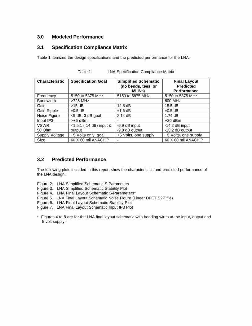
3.0 Modeled Performance 3.1 Specification Compliance Matrix Table 1 itemizes the design specifications and the predicted performance for the LNA.
Table 1. LNA Specification Compliance Matrix Characteristic Specification Goal Simplified Schematic
(no bends, tees, or MLINs)
Final Layout Predicted
Performance Frequency 5150 to 5875 MHz 5150 to 5875 MHz 5150 to 5875 MHz Bandwidth >725 MHz - 800 MHz Gain >15 dB 12.8 dB 15.5 dB Gain Ripple ±0.5 dB ±1.6 dB ±0.5 dB Noise Figure <5 dB, 3 dB goal 2.14 dB 1.74 dB Input IP3 >+5 dBm - +20 dBm VSWR, 50 Ohm
<1.5:1 ( 14 dB) input & output
-6.9 dB input -9.8 dB output
-14.2 dB input -15.2 dB output
Supply Voltage +5 Volts only, goal +5 Volts, one supply +5 Volts, one supply Size 60 X 60 mil ANACHIP - 60 X 60 mil ANACHIP 3.2 Predicted Performance The following plots included in this report show the characteristics and predicted performance of the LNA design. Figure 2. LNA Simplified Schematic S-Parameters Figure 3. LNA Simplified Schematic Stability Plot Figure 4. LNA Final Layout Schematic S-Parameters* Figure 5. LNA Final Layout Schematic Noise Figure (Linear DFET S2P file) Figure 6. LNA Final Layout Schematic Stability Plot Figure 7. LNA Final Layout Schematic Input IP3 Plot * Figures 4 to 8 are for the LNA final layout schematic with bonding wires at the input, output and 5 volt supply.

Figure 2. LNA Simplified Schematic S-Parameters
m7freq=5.100GHznf(2)=2.141
m3freq=5.100GHzdB(S(1,1))=-6.894
m4freq=5.900GHzdB(S(1,1))=-8.819
m1freq=5.100GHzdB(S(2,1))=12.771m2freq=5.900GHzdB(S(2,1))=15.828
m5freq=5.100GHzdB(S(2,2))=-9.828
m6freq=5.900GHzdB(S(2,2))=-16.457
m8freq=5.100GHzNFmin=1.668
3 4 5 6 7 8
-25
-20
-15
-10
-5
0
5
10
15
20
freq, GHz
nf(2
)
m7
dB(S
(1,1
))
m3m4
dB(S
(2,1
))m1
m2
dB(S
(2,2
))
m5
m6
NFm
in
m8
S-Parameter (Simplified Schematic)
Figure 3. LNA Simplified Schematic Stability Plot
3 4 5 6 7 8
0
1
2
3
4
5
6
freq, GHz
our_
mu
our_
mup
LNA Simplified Schematic Stability Plot
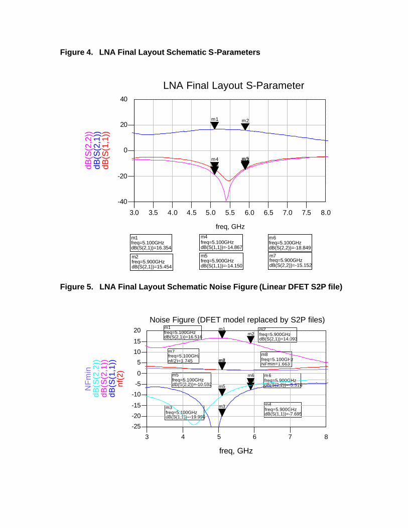
Figure 4. LNA Final Layout Schematic S-Parameters
m4freq=5.100GHzdB(S(1,1))=-14.867
m5freq=5.900GHzdB(S(1,1))=-14.150
m1freq=5.100GHzdB(S(2,1))=16.354
m2freq=5.900GHzdB(S(2,1))=15.454
m6freq=5.100GHzdB(S(2,2))=-18.849
m7freq=5.900GHzdB(S(2,2))=-15.152
3.0 3.5 4.0 4.5 5.0 5.5 6.0 6.5 7.0 7.5 8.0
-40
-20
0
20
40
freq, GHz
dB(S
(1,1
))
m4 m5
dB(S
(2,1
))
m1 m2
dB(S
(2,2
))
m6m7
LNA Final Layout S-Parameter
Figure 5. LNA Final Layout Schematic Noise Figure (Linear DFET S2P file)
m7freq=5.100GHznf(2)=1.745
m3freq=5.100GHzdB(S(1,1))=-19.996
m4freq=5.900GHzdB(S(1,1))=-7.695
m1freq=5.100GHzdB(S(2,1))=16.516
m2freq=5.900GHzdB(S(2,1))=14.093
m5freq=5.100GHzdB(S(2,2))=-10.592
m6freq=5.900GHzdB(S(2,2))=-5.516
m8freq=5.100GHzNFmin=1.663
3 4 5 6 7 8
-25
-20
-15
-10
-5
0
5
10
15
20
freq, GHz
nf(2
)
m7
dB(S
(1,1
))
m3
m4
dB(S
(2,1
))
m1m2
dB(S
(2,2
))
m5
m6
NF
min
m8
Noise Figure (DFET model replaced by S2P files)

Figure 6. LNA Final Layout Schematic Stability Plot
3 4 5 6 7 8
1
2
3
4
5
6
freq, GHz
our_
mu
our_
mup
LNA Final Layout Stability Plot
Figure 7. LNA Final Layout Schematic Input IP3 Plot
-50 -45 -40 -35 -30 -25 -20 -15 -10 -5 0 5 10 15 20-200
-150
-100
-50
0
50
RFpower
Spe
ctru
m[1
]S
pect
rum
[3]
LNA Final Layout IP3

4.0 Schematic Diagrams The following schematics are included in this report. Figure 8. LNA Simplified Schematic Figure 9. LNA Final Layout Schematic Figure 10. LNA Final Layout Schematic with DFET model replaced by S2P file Figure 11. LNA Final Layout in ANACHIP 5.0 DC Analysis For the input and output stages, Vd, Vgs and Ids were selected for the maximum gain and lowest noise figure that could be achieved simultaneously. Table 2 summarizes the DC bias check for the LNA.
Table 2. DC Bias Check
Input Stage Output Stage Vd = 3.18V Vgs = -0.27V Ids = 17.46mA
Vd = 4.85V Vgs = -0.29V Ids = 18.58mA
The currents through all resistors were checked to verify that the resistor widths selected adhered to the layout guidelines. The guideline followed was that the minimum allowable resistor width be1µm per 1ma current through the resistor. In particular, the 100 ohm voltage dropping resistor for Ids of the first stage was 25µm and drew 18ma. Also the first and second stage 15 ohm source resistors were 25µm and drew 18ma. The feedback resistor for the second stage was 5µm and drew only 1.3µa. Figure 12 is the simplified schematic showing the voltages and currents throughout the layout.
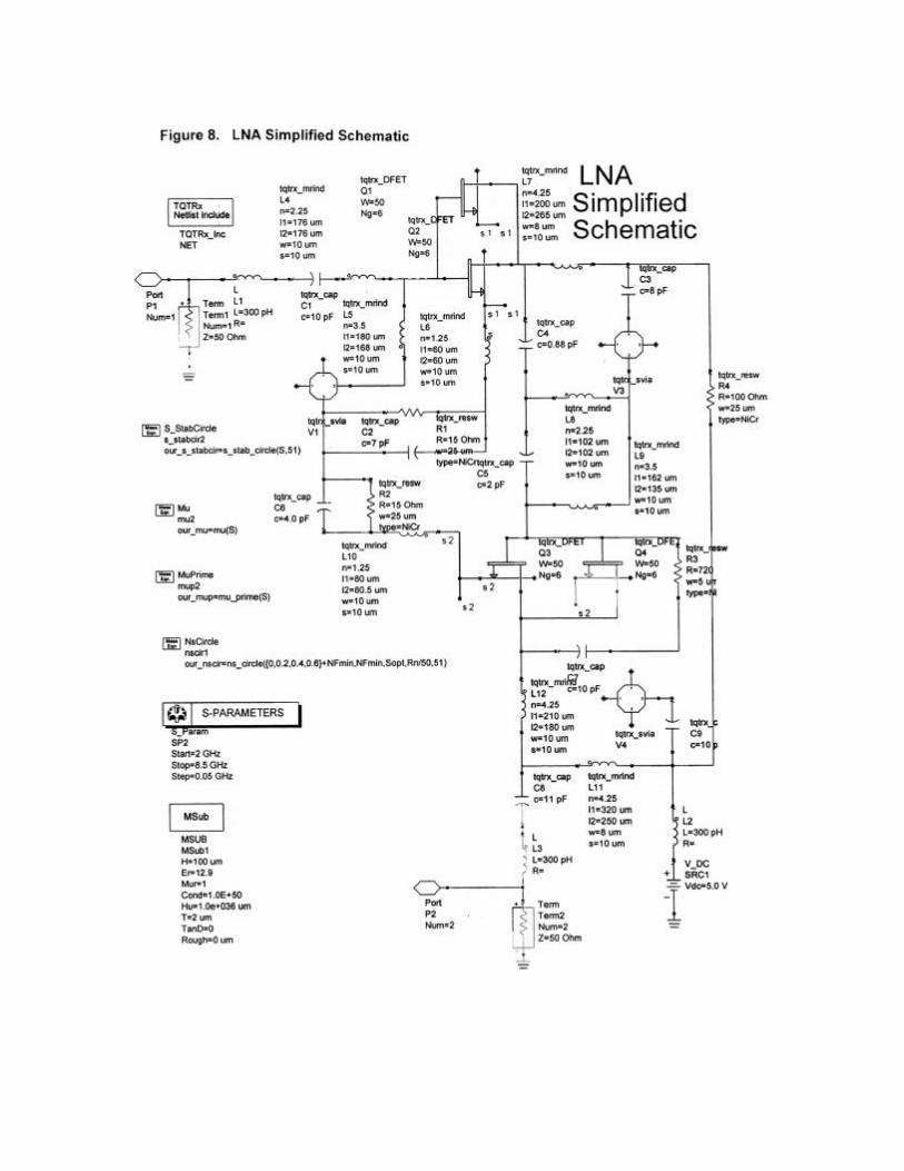

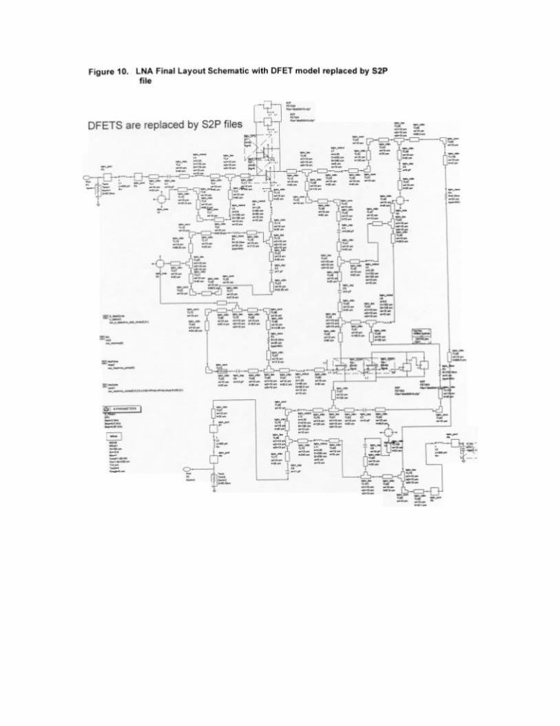
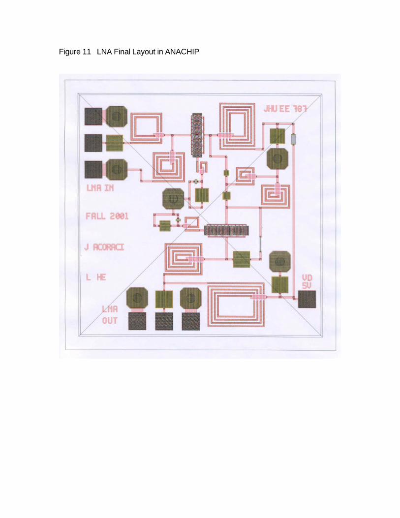
Figure 11 LNA Final Layout in ANACHIP


6.0 Test Plan 6.1 Test Equipment The following test equipment or equivalent is necessary to measure the LNA performance:
• Agilent 8510 Network Analyzer • Agilent XXX Noise Figure Meter • 5 volt DC power supply
6.2 Turn On Procedure Extreme caution should be taken when turning on the 5 volt DC powers supply so as not to draw excessive current.
• The required voltage for the LNA is +5 V DC • The required current for the LNA is 36.04 mA
6.3 S-Parameter Measurement
• Calibrate the network analyzer from 1 to 10 GHz • Position the bias probe on the “VD 5V” pad • Position the input probes on the “LNA IN” input pads • Position the output probes on the “LNA OUT” pads • Make S11, S21, S12, S22 measurements and store all data on disk
6.4 Noise Figure Measurement
• Calibrate the noise figure meter • Position the bias probe on the “VD 5V” pad • Position the input probes on the “LNA IN” input pads • Position the output probes on the “LNA OUT” pads • Make noise figure measurements and store all data on disk
7.0 Conclusion and Recommendations The LNA design process was very successful in that all design goals were met. In particular the noise figure of 1.7 dB was much lower than the goal of 3 dB. Also the input IP3 of +20 dBm was much higher the goal of +5 dBm. A recommendation to be more efficient in the design process is to spend less time with the ideal element design and more time with the TriQuint elements and the real layout with bends, tees, and MLINs. 8.0 Project File The project file has been submitted on a 3 ½ HD Diskette. 9.0 GDSII (CALMA) Layout File The GDSII layout file has been submitted on a 3 ½ HD Diskette
JOHN HOPKINS UNIVERSITY
WHITING SCHOOL OF ENGINEERING PART-TIME PROGRAMS IN ENGINEERING
MMIC Design JHU 525.787 (M 4:30-7:15 PM)
C-Band Up/Down Converter: Final Report
SUBMITTED BY:
Willie Lee Thompson, II [email protected]
Morgan State University Center of Microwave, Satellite and RF Engineering
Schaefer 353

C-Band MMIC Up/Down Converter
W. Thompson ii
ABSTRACT
A singly balanced 180-degree monolithic microwave integrated circuit (MMIC) is
presented in this paper. The mixer exhibits up and down conversion capabilities for RF
frequencies ranging from 5150 MHz to 5875 MHz, LO frequencies ranging from 5425 MHz
to 5625 MHz and IF frequency of 275 MHz, respectively. Simulations exhibit a conversion
loss of < 10 dB for a LO power of 3 dB for both up and down conversion with an LO-to-RF
isolation > -22 dB. The MMIC circuit fits on a 60 mils x 60 mils chip with a +5 V power
supply and will be implemented in a simplex transceiver for HiperLAN wireless local area
network (WLAN).

C-Band MMIC Up/Down Converter
W. Thompson iii
CONTENTS Abstract........................................................................................................ii Contents......................................................................................................iii 1.0 Introduction....................................................................................... 1
1.1 Circuit Architecture ....................................................................... 1 1.2 Design Philosophy ......................................................................... 2 1.3 Trade-offs....................................................................................... 4
2.0 Modeled Performance....................................................................... 5
2.1 Specification Matrix ....................................................................... 5 2.2 Predicted Performance ................................................................. 6
2.2.1 180-degree Hybrid Performance ............................................ 6 2.2.2 Filters Performance ................................................................ 6 2.2.3 Down Converter Performance ................................................ 7 2.2.4 Up Converter Performance..................................................... 9 2.2.5 Isolation and VSWR Performance......................................... 11
3.0 Final Layout ..................................................................................... 12 4.0 DC Analysis ..................................................................................... 13 5.0 Test Plan.......................................................................................... 15
5.1 Spectrum Test Configuration....................................................... 15 5.2 Isolation and VSWR Test Configuration....................................... 16
6.0 Conclusion ...................................................................................... 17 References................................................................................................ 18

C-Band MMIC Up/Down Converter
W. Thompson 1
1.0 INTRODUCTION The HiperLAN transceiver will be used to receive and send data within two RF bands.
The lower band ranges from 5150 MHz to 5350 MHz, while the upper band ranges from
5725 MHz to 5875 MHz. The mixer is responsible for down converting the RF signal with
the two bands to an IF signal in receive mode and up converting the IF signal to a RF
signal within the bands in send mode. As a result, the circuit architecture used for the
mixer must be able to up and down convert without any modification to the topology.
1.1 CIRCUIT ARCHITECTURE The circuit architecture selected for the mixer is a singly balanced 180-degree mixer,
best known as a “rat-race” mixer. The mixer consists of a lumped element 180-degree
hybrid, two 80-µm DFETs diodes, a low-pass filter for IF port filtering and two high-pass
filters for LO and RF port filtering, respectively. Figure 1.1 illustrates the general
topology of a singly balanced 180-degree mixer.
DC
LO
RF
IF
1800 Hybrid HPF
HPF
LPF
Off Chip
Figure 1.1.1: Singly balanced 180-degree mixer architecture.

C-Band MMIC Up/Down Converter
W. Thompson 2
This architecture utilizes the nonlinear conductance of the diodes for mixing. Diodes are
more stable than field-effect transistors (FETs) and allows for mixing in both directions.
The shunt configuration of the diodes allows for easier impedance matching to the 50-Ω
at the hybrid’s ports. Proper biasing and sizing of the DFETs can achieve impedance
match. We concluded that an 80-µm DFET with 2 gate fingers connected in diode
configuration provided the best impedance match.
LO signal is located at the ∆ port and the RF/IF signals are located at the Σ port of the
180-degree hybrid, respectively. As a result, the hybrid splits the LO power between the
two diodes ports with a 180-degree phase shift, while RF/IF powers are split between the
diodes ports in phase. Filtering is implemented at the RF/IF port to separate the signals
after mixing. In addition, filtering at the ports improves the RF-to-IF isolation and LO-to-IF
isolation. LO-to-RF isolation is achieved by the properties of the hybrid, where the ∆ and
Σ ports are mutual isolated from each other.
Biasing of the diodes is used for starved LO operation of the mixer, which allows for
smaller LO powers. The DC bias supply is coupled between the diodes via the hybrid and
the blocking capacitors at each ports. An off chip blocking capacitor must be used due
to low frequency of the IF signal, which requires a high value capacitor that cannot fit
onto the chip.
1.2 DESIGN PHILOSOPHY The design philosophy was determined by the specifications for the mixer. The
specification of interested were:
• Up and down conversion abilities
• Layout Constraints
• High LO-to-RF isolation
• Low conversion loss
Concerning the above specifications, it was determine that the following architectures
were candidates for the mixer: 1) 90-degree mixer, 2) singly balanced 180-degree mixer
and 3) doubly balanced mixer.

C-Band MMIC Up/Down Converter
W. Thompson 3
One of the major advantages of balanced mixers has over single-component mixers is its
inherent rejection of spurious responses. A spurious response is a mixing product
between a harmonic of the RF and a harmonic of the LO, which can distorts signals of
interest if mixed to the proper frequencies. In addition, balanced mixer provides inherent
port isolations. However, the 90-degree mixer exhibits poor spurious response and the
port isolation is only as good as the VSWR at each port, while the singly balanced 180-
degree mixer exhibits both characteristics well.
Next, the layout constraint of 60 mils x 60 mils was another important specification for
developing the mixer. The doubly balanced mixer requires the use of a balun. A balun is
a large coupling structure that cannot be implemented due to the layout constraints. In
addition, the TriQuint design library does not have any models for a balun structure. To
develop a library model would require the use of a electromagnetic simulator to model
the coupling behavior of the balun, or fabrication of a structure for modeling. As a
result, the doubly balanced mixer was not selected. However, the singly balanced 180-
degree mixer requires a 180-degree hybrid, which can be easily implemented using
lumped elements included within the TriQuint design library.
Figure 1.2: Classical architecture for a singly balanced 180-degree mixer.
The classical approach for implementing a singly balanced 180-degree mixer is
illustrated in Figure 1.2. The diodes are tied together to form the IF port, while the LO
C-Band MMIC Up/Down Converter
W. Thompson 4
and RF are connected to the ∆ and Σ ports, respectively. However, we implemented a
novel approach for connecting the diodes. The diodes were connected in a shunt
configuration as shown in Figure 1.1. The shunt configuration allows for good
impedance matching of the diode independently for each other and easy implementation
of DC bias via the hybrid.
1.3 TRADE-OFFS
The major trade-off for the design was the layout constraint of the MMIC. The doubly
balanced mixer is an excellent general-purpose mixer design. It exhibits wide bandwidth,
good spurious response injection and good port isolation. However, the implementation
of a balun cannot be achieved. The 180-degree mixer exhibits a narrower bandwidth,
which requires the RF/LO frequencies to be within 15% of each other. The bandwidth
requirement is met by the frequency specifications for the mixer and the layout of the
180-degree hybrid is easily implemented with lumped elements.
A couple of minor trade-offs were made: 1) the sizing of the diodes for impedance
matching, 2) layout design of the hybrid, and 3) inductor values for the RF/LO and IF
filters. The input and output impedances of the diodes vary with DC bias and diode size.
As a result, special interested with taken to bias and size the diodes to provide proper
impedance to the hybrid’s ports. Secondly, the hybrid requires the use of four shunt
capacitors to ground. A layout design was implemented to share a center via to ground
between the shunt capacitors. This configuration prevented the usage of multiple vias,
which require significant amount of die area. Lastly, the optimum inductor values were
calculated for each filter types. Due to layout constraints, the inductor values were
modified with minimum effect on the overall transfer response of the filters. However,
changing the inductors values affect the input impedance of the filters and the VSWRs of
the ports. The VSWR specifications were still met, but were not ideal.

C-Band MMIC Up/Down Converter
W. Thompson 5
2.0 MODELED PERFORMANCE
2.1 SPECIFICATION MATRIX Table 2.1 summarizes the design specifications and simulated performance of the singly balanced 180-degree mixer. All specifications for the design were met.
Table 2.1: Specification matrix and simulated performance results.
Specification Goal Acceptable Simulated
Frequency Bandwidths
Lower RF Band 5150 – 5350 MHz
Upper RF Band
5725 – 5875 MHz
LO Band 5425 – 5625 MHz
IF Band 275 MHz
Lower RF Band 5150 – 5350 MHz
Upper RF Band
5725 – 5875 MHz
LO Band 5425 – 5625 MHz
IF Band 275 MHz
Lower RF Band 5150 – 5350 MHz
Upper RF Band
5725 – 5875 MHz
LO Band 5425 – 5625 MHz
IF Band 275 MHz
LO-to-RF Isolation
-16 dB - 10 dB > -22 dB
Conversion Loss
-7 dB - 10 dB 9.10 dB*
LO Power
0 dBm +7 dBm 3 dBm**
VSWR
1.5:1 2.5:1 ~1.75:1
Supply Voltage
5 V 0 – 5 V 5 V
Size
60 mils x 60 mils 60 mils x 60 mils 60 mils x 60 mils
*Conversion loss is an average of up and down conversion simulation results for both RF bands. **LO power is the LO power that met conversion loss specification for both up and sown conversions.

C-Band MMIC Up/Down Converter
W. Thompson 6
2.2 PREDICTED PERFORMANCE
2.2.1 180-DEGREE HYBRID PERFORMANCE The simulated performance of the 180-degree hybrid is illustrated in Figure 2.1. As
previously discussed, the LO signal is connected to the ∆ port (S11), the RF and IF signals
are connected to the Σ port (S44), and the diodes are connected the port 2 (S22) and port 3
(S33), respectively. The powers division of the ∆ and Σ ports at the diode ports are
approximately -3 dB and -4.2 dB, respectively. The phase differences at the diode ports
are ~180 degree and ~0 degree across the operating band of the mixer, respectively.
Figure 2.1: Simulated performance of the 180-degree hybrid.
2.2.2 FILTERS PERFORMANCE
The simulated performance of the filters is illustrated in Figure 2.2. The LO and RF filters
are high-pass filters using series capacitor and shunt inductor configuration. The IF
filters is a low-pass filter using series inductor and shunt capacitor configuration. Each
filter was design to provide approximately –20 dB of attenuation for the undesired
frequencies. As illustrated in Figure 2.2, the LO/RF filters provide approximately –30 dB
of attenuation at the IF frequency of 275 MHz, while the IF filter provides at least –20 dB
of attenuation across the operating band of the mixer.

C-Band MMIC Up/Down Converter
W. Thompson 7
Figure 2.2: Simulated performance of the filters used in the singly balanced 180-degree mixer.
2.2.3 Down Converter Performance
The mixer’s performances as a down converter are illustrated in Figure 2.3 and Figure
2.4. In Figure 2.3, the mixer is configured for down converting frequencies in the lower
band, while in Figure 2.4, it is configured for down converting frequencies in the upper
band. The LO and RF powers were +3 dBm and –20 dBm for both configurations. The
conversion losses were –8.22 dB and -8.75, respectively.
Figure 2.3: Simulated performance of mixer as a down converter for lower band frequencies.

C-Band MMIC Up/Down Converter
W. Thompson 8
Figure 2.4: Simulated performance of mixer as a down converter for upper band frequencies.
The conversion loss is a function of LO power. To find optimum performance for the
mixer, simulations of the conversion loss as a function of LO power were performed. The
results of the simulations are plotted in Figure 2.5. The optimum LO powers for the down
converter were +3 dBm for the lower band and +5.5 dBm for the upper band. In addition,
several other simulations were performed for verification of design and are summarized
in Table 2.2.
Figure 2.5: Simulation results of conversion loss as a function of LO power.

C-Band MMIC Up/Down Converter
W. Thompson 9
Table 2.2: Summary of simulated performances for down converter configurations.
RF Frequency LO Frequency IF Frequency Conversion Loss
5250 MHz 5525 MHz 275 MHz -8.22 dB
5800 MHz 5525 MHz 275 MHz -8.75 dB
5150 MHz 5425 MHz 275 MHz -8.21 dB
5875 MHz 5600 MHz 275 MHz -9.22 dB
*LO power was +3 dBm and RF power was –20 dBm for all simulations.
2.2.4 Up Converter Performance
The simulated performance of the mixer as a up converter is illustrated in Figure 2.6. The
up converter produces both lower and upper band RF frequencies for a given LO and IF
configuration. The lower band is given by fLOWER = fLO – fIF and upper band is given by
fUPPER = fLO + fIF. The LO and IF powers for the simulation were +3 dBm and 0 dBm,
respectively. Conversion loss as a function of LO power is illustrated in Figure 2.7 and
Table 2.3 summarizes the simulated performance of several simulation configurations.
Figure 2.6: Simulated performance of mixer as a up converter.

C-Band MMIC Up/Down Converter
W. Thompson 10
Figure 2.7: Simulation results for conversion loss as a function of LO power.
Table 2.3: Summary of simulated performances for up converter configurations.
LO Freq IF Freq Lower Freq Upper Freq Conversion Loss 5525 MHz 275 MHz 5250 MHz 5800 MHz 9.79 dB 5425 MHz 275 MHz 5150 MHz 5700 MHz 9.72 dB 5600 MHz 275 MHz 5325 MHz 5875 MHz 9.81 dB
*LO power was +3 dBm and IF power was 0 dBm for all simulations.
Figure 2.7 demonstrates that the up converter requires more LO power to obtaining the
minimum specification of a conversion loss, while the down converter configuration met
the specification with a LO power of 0 dBm. In addition, the optimum LO power for the up
converter seems to be greater than the allowable LO power of 7 dB.

C-Band MMIC Up/Down Converter
W. Thompson 11
2.2.5 ISOLATION AND VSWR PERFORMANCE The simulated performance for the LO isolation and VSWRs is illustrated in Figure 2.8.
The LO-to-RF isolation is greater than –20 dB across the operating band and LO-to-IF
isolation is greater than –35 dB across the operating band. The VSWR specification of
2.5:1 is met for each port.
Figure 2.8: Simulated performance for LO isolation and VSWR for each port.
C-Band MMIC Up/Down Converter
W. Thompson 12
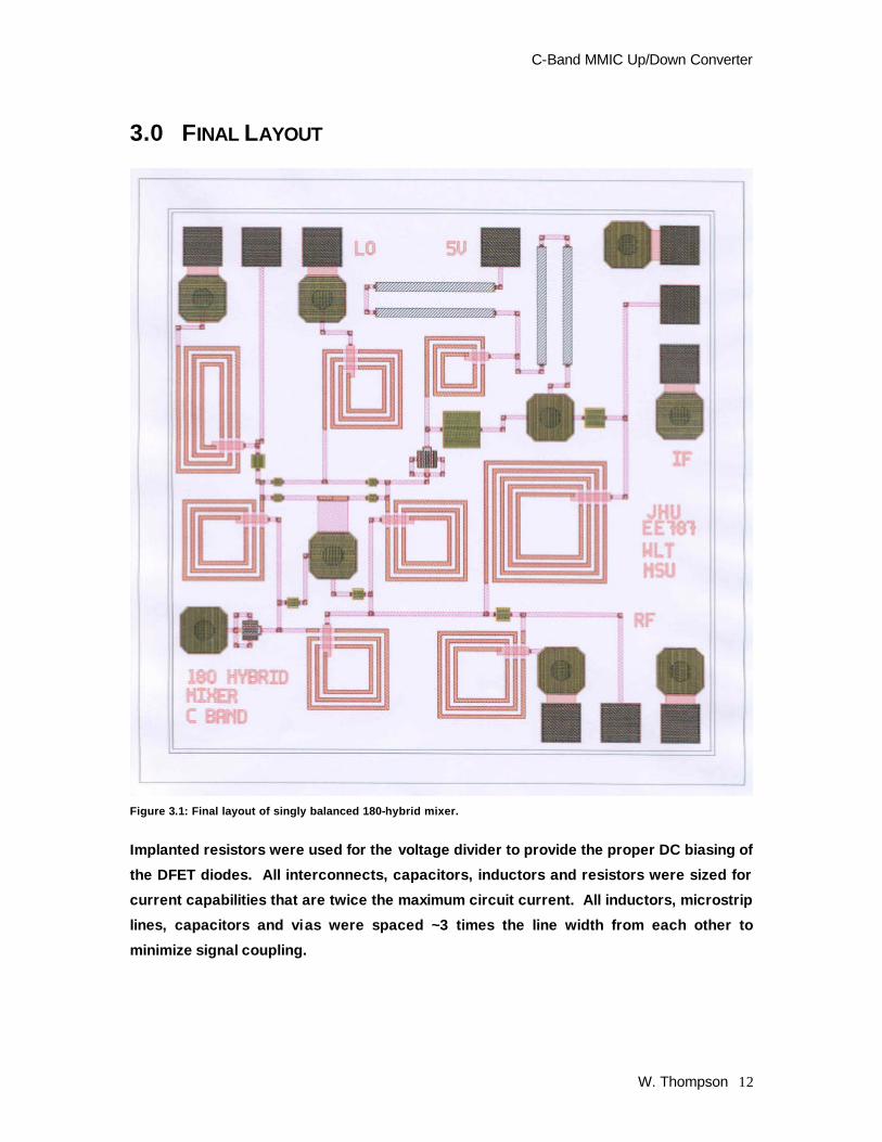
3.0 FINAL LAYOUT
Figure 3.1: Final layout of singly balanced 180-hybrid mixer.
Implanted resistors were used for the voltage divider to provide the proper DC biasing of
the DFET diodes. All interconnects, capacitors, inductors and resistors were sized for
current capabilities that are twice the maximum circuit current. All inductors, microstrip
lines, capacitors and vias were spaced ~3 times the line width from each other to
minimize signal coupling.

C-Band MMIC Up/Down Converter
W. Thompson 13
4.0 DC ANALYSIS The DC bias of the diodes is essential for starved LO operation of the mixer. The DFET
diodes were bias at a DC voltage of 0.65 V and a DC current of ~800 µA. This bias point
provided the best impedance match at the hybrid’s ports and the nonlinear conductance
that is required for mixing. Figure 4.1 – Figure 4.3 show the DC analysis results for a
simplified schematic architecture of the singly balanced 180-degree mixer. The DC
current and voltage is coupled between the diodes via the hybrid and the blocking
capacitors at each port. A DC voltage of 1.3 V is supplied by a voltage divider and a +5V
power supply. The 1.3 V will be approximately dropped evenly across both diodes
resulting in biasing voltages of 0.65 V for each diode and DC current of ~800 µA.
Figure 4.1: DC analysis results for a simplified schematic diagram of the singled balanced 180-degree mixer.

C-Band MMIC Up/Down Converter
W. Thompson 14
Figure 4.2: DC analysis results for voltage divider and DFET diode @ port 3.
Figure 4.3: DC analysis results for DFET diode @ port 2.
C-Band MMIC Up/Down Converter
W. Thompson 15
5.0 TEST PLAN
5.1 SPECTRUM TEST CONFIGURATION
180-DegreeMixer
LO SignalGenerator
RF SignalGenerator
DC BlockingCapacitor
SpectrumAnalyzer
+5 VPower Supply
DUTRF
IFLO
PowerMeter
3 dBCoupler
3 dBCoupler
PowerMeter
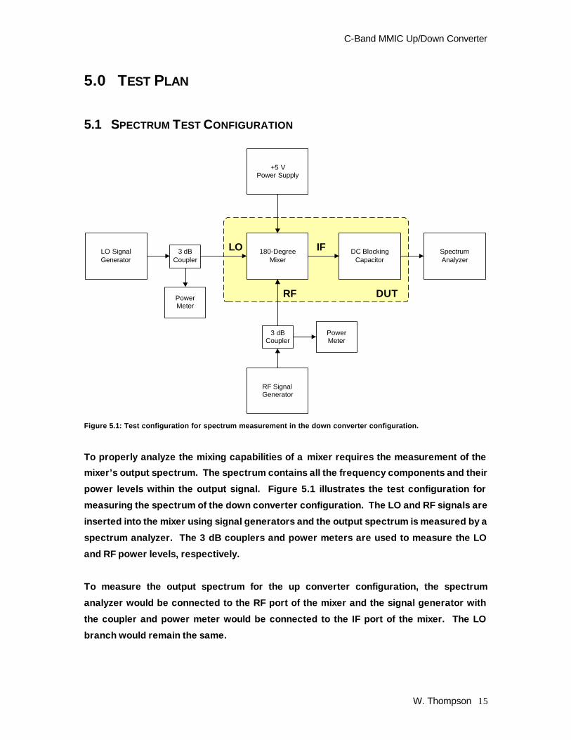
Figure 5.1: Test configuration for spectrum measurement in the down converter configuration.
To properly analyze the mixing capabilities of a mixer requires the measurement of the
mixer’s output spectrum. The spectrum contains all the frequency components and their
power levels within the output signal. Figure 5.1 illustrates the test configuration for
measuring the spectrum of the down converter configuration. The LO and RF signals are
inserted into the mixer using signal generators and the output spectrum is measured by a
spectrum analyzer. The 3 dB couplers and power meters are used to measure the LO
and RF power levels, respectively.
To measure the output spectrum for the up converter configuration, the spectrum
analyzer would be connected to the RF port of the mixer and the signal generator with
the coupler and power meter would be connected to the IF port of the mixer. The LO
branch would remain the same.

C-Band MMIC Up/Down Converter
W. Thompson 16
5.2 ISOLATION AND VSWR TEST CONFIGURATION
180-DegreeMixer
DC BlockingCapacitor
8510 NetworkAnalyzer
+5 VPower Supply
DUTRF
IFLO
50 OhmsTermination
Port 2
Port 1
Figure 5.2: Test configuration for measurement of LO isolation and VSWRs
The LO isolation and VSWRs can be measured by using a network analyzer. The network
analyzer will measure the LO isolation and VSWRs as a function of frequency. The LO-to-
RF isolation can be obtained by measuring the forward transmission coefficient (S21) and
the VSWRs at each port can be obtained by measuring the input and output reflections
coefficients (S11 and S22) as illustrated in Figure 5.2. The 8510 network analyzer is a two-
port measurement instrument and requires the proper termination of the IF port of the
mixer for the down converter configuration. VSWR is calculated using the following
equation:
Γ−Γ+
=11
VSWR (5.1)
where Γ is the reflection coefficient at that port.
The LO-to-IF isolation and VSWRs for the up converter configuration can be measure by
connecting the network analyzer to the IF port and terminating the RF port.
C-Band MMIC Up/Down Converter
W. Thompson 17
6.0 CONCLUSION A complete MMIC design for a C-Band singly balanced 180-degree mixer was presented
with a conversion loss of < 10 dB @ LO power of +3 dBm for both up and down
conversion configurations. All other specifications for the mixer were met as
demonstrated in Section 2 of this report. The novel shunt diode architecture was used to
improve the impedance matching of the diodes at the hybrid’s ports, which allowed for
better conversion loss.
The conversion loss was a strong function of LO power. It was demonstrated that a LO
power of +3 dBm was optimum for both up and down converting to met the conversion
loss specification. The up converter configuration required more LO power than the
down converter configuration.
An improvement to this design could be better matching of the filters to 50 Ω, which may
decrease the conversion loss even further for both configurations. Also using better
filter architectures (i.e. 3 section Butterworth filter) could improve the LO isolation and
conversion loss, but requires more die area.

C-Band MMIC Up/Down Converter
W. Thompson 18
REFERENCES
S. A. Mass, Microwave mixers, 2nd Ed Artech House: Boston, 1993.
S. A. Mass, The RF and microwave circuit design cookbook, Artech House:
Boston, 1998.
R. Gabany, “C band MMIC up/down converter final report”, JHU/APL Project
Report, 2000.
C. Moore and J. Penn, Class Handouts, JHU/APL, 2000.

1
C-BAND POWER AMPLIFIER 525.787 Microwave Monolithic Integrated Circuits (MMIC) Design
Gary S. Hoffman
Fall 2001
ABSTRACT – MMIC Class-F, cascade C-Band power amplifier designed for final class project using TriQuint parts. Frequency band of 5.15 to 5.875 GHz, or a bandwidth of 725.0 MHz, with a center frequency of 5.5125 GHz. Amplifier small signal gain >12.0 dB across the band with an output power > +24.0 dBm at center frequency, 1.0 dB compression point. On-chip resonant circuits in series and parallel, tuned to center frequency and its 3rd harmonic respectively, shape the output waveform and improve Power Added Efficiency (PAE). On-chip input and output matching networks into 50.0 Ohms, minimize VSWR to <1.5:1 across the band.
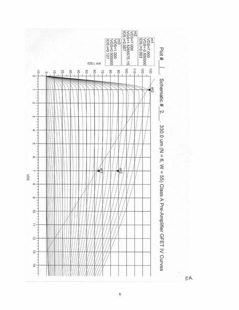
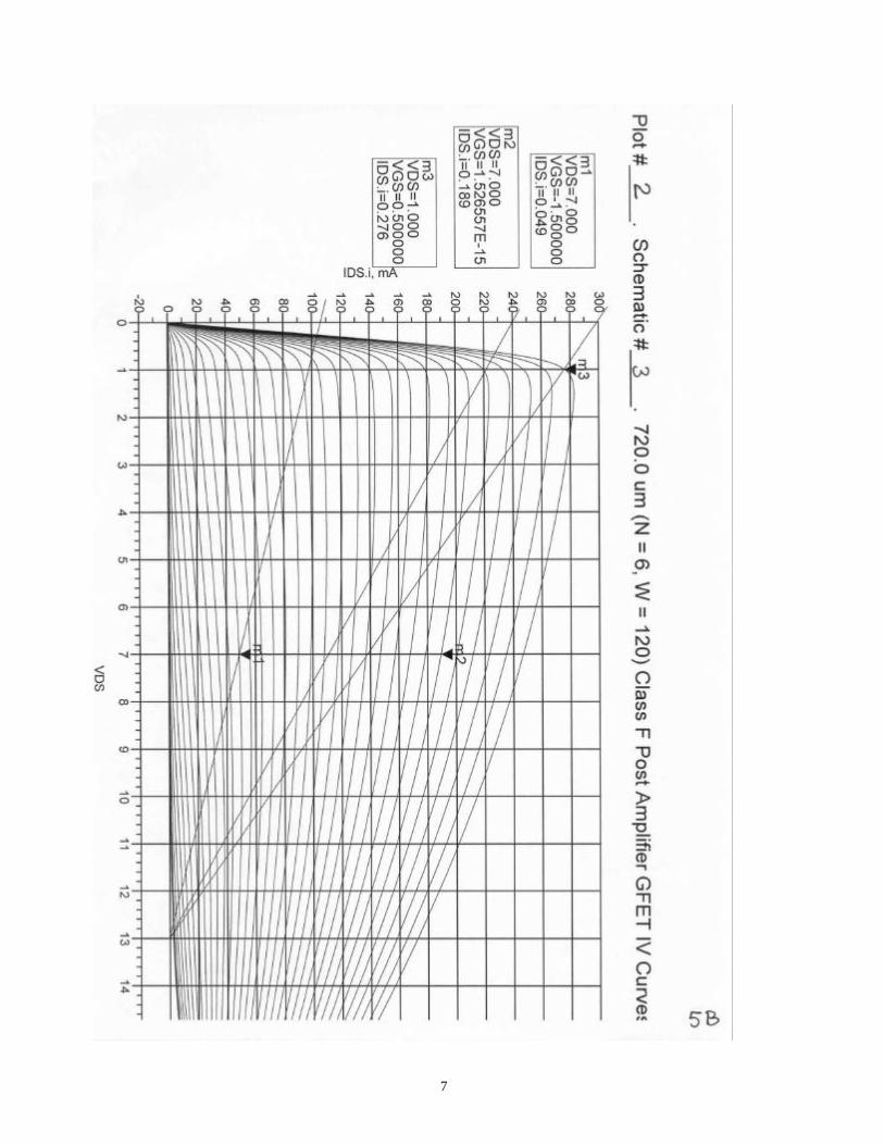
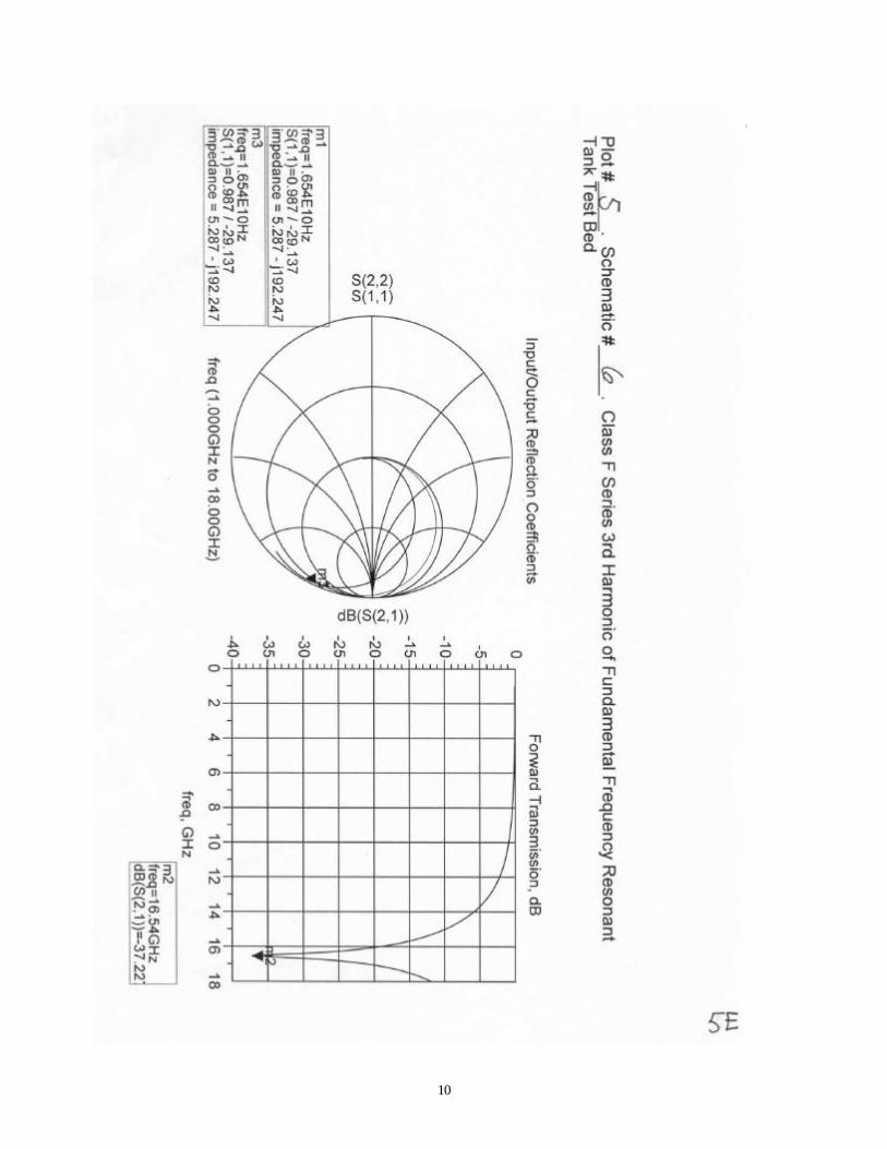
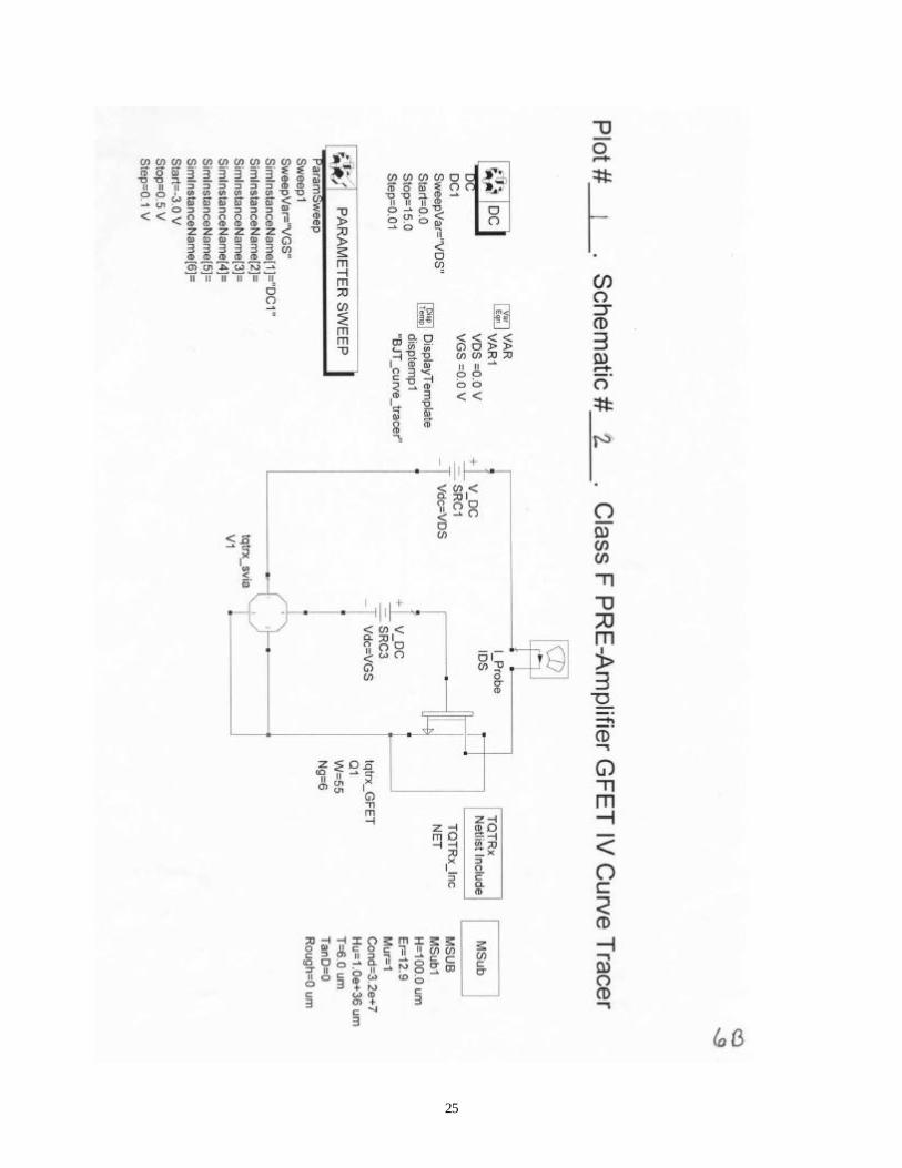
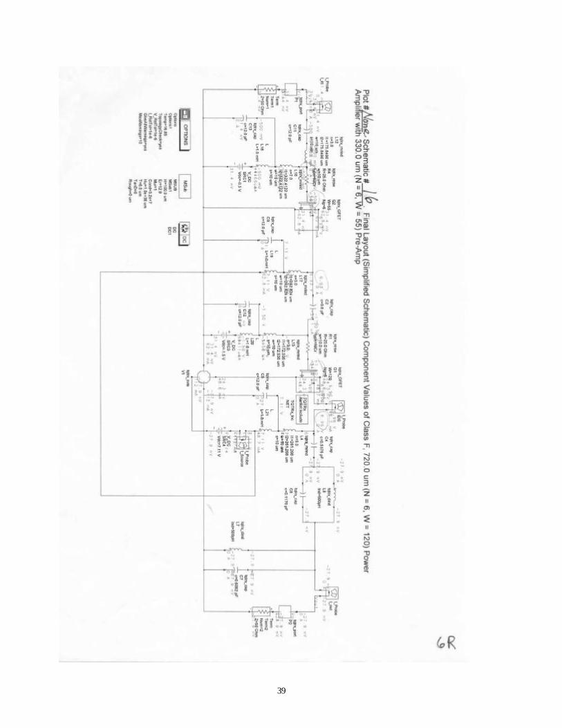
1. INTRODUCTION CIRCUIT DESCRIPTION – With reference to a simplified final layout shown in Schematic #1 on page 6A, this C-Band power amplifier is a cascade Class-F power amplifier, which has a Class-A biased pre-amplifier (Q2) with a Class-AB biased post-amplifier (Q1). This design allowed for an overall small signal gain >12.0 dB to be divided between two amplifier stages. Center frequency of amplifier is 5.5125 GHz with a 725.0 MHz bandwidth (5.15-5.875 GHz). On-chip input matching (L12, L16), output matching (L4) with resonant circuits in series (L8, C8) and parallel (L7, C7), plus DC blocking and by-pass capacitors (C2, C4, C5, C9, C11, C12, C13). 1.0 mH inductors (L18 - L21) shown in DC bias paths are bond wire models, while input and output tqtrx_ports (P1, P2) are models of G-S-G signal-probe pads [5, 6]. For individual TriQuint GFET amplifiers; Class-A biased pre-amplifier, as given by marker #1 in IV Curves of Plot #1 on page 5A, has a DC bias point of –0.5 V for VGS, +7.0 V for VDS and 63.0 mA for IDS. Schematic #2 on page 6B gives the number of gates and gate widths for this 330.0 um GFET as 6 and 55.0 um respectively. Class-AB biased post-amplifier, as given by marker #1 in the IV Curves of Plot #2 on page 5B, has a DC bias point (25.0% of the IDSS value shown at marker #2) of –1.5 V for VGS, +7.0 V for VDS, and 49.0 mA for IDS. Schematic #3 on page 6C for this 720.0 um GFET gives number of gates and gate widths as 6 and 120.0 um respectively [5, 6]. Returning to Schematic #1 on page 6A, Input Matching Network (IMN) formed by L12 and L16 match pre-amplifier (Q2) to a 50.0 Ohm source impedance. L17, C2 and L15 form an inductive pi-network between pre-amplifier Q2 and post-amplifier Q1. L4 on output of post-amplifier Q1 has an RCripp load value of 50.0 Ohms and matches Q1 to an output load impedance of 50.0 Ohms through an output resonant network of series circuit L8 and C8, plus parallel circuit of L7 and C7 [5, 6]. This output resonant network shapes the output waveform and improves overall Power Added Efficiency (PAE). It is composed of resonant circuit L8 and C8 tuned to 16.54 GHz (3rd harmonic of 5.5125 GHz), and resonant circuit L7 and C7 tuned to center frequency (i.e. 5.5125 GHz). With these two resonant circuits, this network provides an OPEN to the 3rd harmonic (16.54 GHz) and a SHORT to the 2nd harmonic (11.03 GHz) but prevents their appearance at the load. For center frequency of 5.5125 GHz, this resonant network provides a MATCH to a 50.0 Ohm load. C4 is a DC blocking capacitor, but is also part of this resonant network and tunes-out any added inductance between the Q1 drain and load presented by this output resonant network [1, 2, 3, 4].

2
Plot #3 on page 5C along with Schematic #4 on page 6D, show the full final layout for this C-Band, cascade Class-F amplifier. Stated design specifications for this C-Band cascade Class-F power amplifier. FREQUENCY BAND: 5.15 to 5.875 GHz [center frequency of 5.5125 GHz], BANDWIDTH: > 725.0 MHz, GAIN, small signal: > 12.0 dB Min [15.0 dB goal], GAIN RIPPLE (flatness): ± 0.5 dB Max, OUTPUT POWER: > +24.0 dBm @ 1.0 dB compression point, EFFICIENCY: > 20.0% @ 1.0 dB compression point [25.0 % goal], VSWR into 50.0 Ohms: < 1.5:1 [ Γ < 0.2, Return Loss < -14.0 dB ] for input and output, SUPPLY VOLTAGES: +7.0 and – 5.0 VDC, SIZE: 60.0 x 60.0 mil ANACHIP. DESIGN PHILOSOPHY – Class-F amplifiers are also termed harmonic control amplifiers. This, from use of a frequency selective network on the amplifier output which is resonant at odd and even harmonics of the fundamental, but blocks these selected harmonics from appearing on the output load. By appearing as an open or a short to these odd/even harmonics, drain voltages and currents are optimized to reduce overall power dissipation in the GFET which results in a higher Power Added Efficiency (PAE). For this design, an open appears for the 3rd harmonic and a short appears for the 2nd harmonic. An open presented to the 3rd harmonic causes flattening of the drain voltage, which if more harmonics were involved, would eventually produce a square wave. A short for the 2nd harmonic causes a flattened sinusoid from added output current flow with a lowered output drain voltage and results in the higher PAE mentioned [1, 2, 3, 4, 5, 6]. Preliminary design of this cascade Class-F amplifier began with the output resonant network described in papers referenced in [1, 2, 3]. Shown in Schematic #5 on page 6E with accompanying Plot #4 on page 5D, resonant circuit L6 and C3 was designed for resonance at the center frequency, Fo, of 5.5125 GHz. At Fo this circuit appears as an open and only the 50.0 Ohm load appears on the output. C2 tuned-out any inductance from this resonant circuit at Fo. Schematic #6 on page 6F with accompanying Plot #5 on page 5E, shows resonant circuit L6 and C3 tuned to provide an open for the 3rd harmonic of Fo. By presenting an open, this circuit prevents 3rd harmonic from appearing across the load. C2 again swamped any residual inductance at resonance. Completed output network appears in Schematic #7 on page 6G with Plot #6 on page 5F, shows combined effect of these two resonant circuits. 2nd harmonic of Fo has a short presented to it through a series L/C resonant circuit consisting of an inductive dominate resonant circuit (L6 and C3) and a capacitive dominate resonant circuit (L7 and C4), with the result that the 2nd harmonic does not appear across the load. Incorporation of this resonant network into the cascade Class-F amplifier design would require added tuning of resonant circuit values, but gave a starting point in overall circuit design. Design of the Input Matching Network (IMN) along with the Output Matching Network (OMN) followed. Using procedures outlined in [5], marker #2 in Plot #7 on page 5G resulting from Schematic #8 on page 6H gave an approximate input value for S11 of the 330.0 um GFET pre-amplifier with which to design an IMN. Taking the conjugate of the value at marker #2 and using a Smith Chart while “looking towards the load and moving towards the GFET gate,” a series inductor (L12) with a shunt inductor (L16) was chosen for the IMN design as shown in Schematic #1 on page 6A. An added benefit of this IMN was the shunt inductor could be used for biasing the gate of this GFET. Bias values stated earlier for the pre-amplifier GFET were –0.5 V for VGS and +7.0 V for VDS and are the values used in Schematic #8 on page 6H.

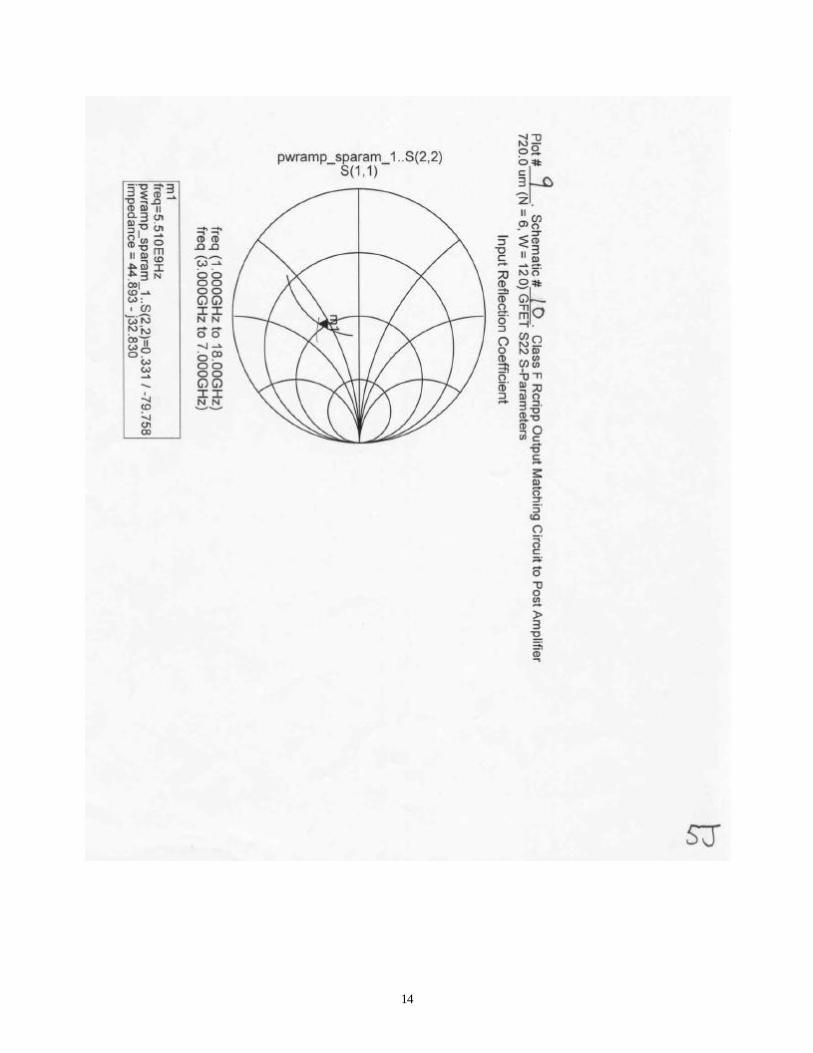
3
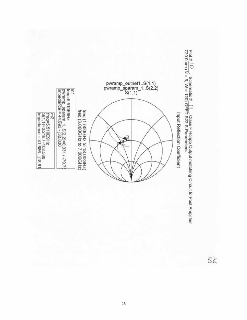
Following Procedures for RCripp outlined in [5], Plot #8 on page 5H resulting from Schematic #9 on page 6J gave, in marker #1, an output S22 value for the 720.0 um GFET post-amplifier with which to design an OMN using an RCripp of 50.0 Ohms. Starting with Plot #9 on page 5J from Schematic #10 on page 6K, a parallel resistor (R1) and capacitor (C1) circuit approximated the output S22 value at 5.5125 GHz from Plot #8 for the 720.0 um GFET. To keep low Q by staying close to the real impedance axis of the Smith Chart, the capacitor value in this circuit was adjusted accordingly. Next, 50.0 Ohms was substituted for the value of R1 in Schematic #11 on page 6L with results shown by marker #2 in Plot #10 on page 5K. Conjugating capacitor C1 in Schematic #11 with an inductor in Schematic #12 on page 6M, gave the result shown by marker #3 in Plot #11 on page 5L. This gave a design point for a shunt inductor using a Smith Chart “while looking towards a 50.0 Ohm load and moving towards the GFET drain” which is given as L4 in Schematic #1 on page 6A. Referring back to Schematic #1 on page 6A, the next step in this cascade Class-F amplifier design was to match the output of the 330.0 um pre-amplifier GFET to the input of the 720.0 um post-amplifier GFET. Looking again at S11 in Plot #8 on page 5H for the 720.0 um post-amplifier, a matching network was designed to the conjugate of the S11 value at marker #2. From work with a Smith Chart, this resulted in the pi-network of L17, C2 and L15 shown in Schematic #1 on page 6A. Adjustments were made in this matching network to attain designed-for gain and power output from this cascade Class-F amplifier. Driving this approach to a between stage matching network was a single load line for this cascade Class-F amplifier on the output of the 720.0 um GFET post amplifier. TRADE-OFFS – Working from a stated design requirement of > +24.0 dBm at the 1.0 dB compression point, gate width of the post-amplifier GFET was gradually increased to its final value of 720.0 um (N = 6, W = 120) as a power margin was sought in Plot #2 on page 5B. This meant that the maximum power output from this GFET was approximately +26.17 dBm at Vsat in Plot #2, or a +2.17 dB margin over the required design output power of >+24.0 dBm. Having a design value for the GFET post-amplifier gate width, bias was the next design item to examine for this post-amplifier. With reference to [1, 2, 3, 4, 5, 6], a Class-F amplifier is traditionally biased as Class-B, or at the pinch-off voltage. This was tried with less than satisfactory results. As an alternative to Class-B biasing, Class-AB biasing at 25.0% of IDSS (marker #2 in Plot #2) was used in the final circuit design. This gave (marker #1 in Plot #2) a VGS of –1.5 V with an IDS of 49.0 mA for a VDS of +7.0 V for this post-amplifier GFET. Having bias and gate width for the post-amplifier GFET, an overall Class-F amplifier gain of 12.0 dB required addition of a pre-amplifier stage to this cascade Class-F amplifier design. Without this pre-amplifier stage, this Class-F amplifier could go into compression with a very low input power level. From STUDENT PROJECTS handout given in class [5], this input level could be as high as +12.0 dBm from input driver and variable gain amplifier stages. From this, +12.0 dBm was chosen as the input power level for an output 1.0 dB compression point > +24.0 dBm from this cascade Class-F power amplifier design. Choosing Class-A bias for the pre-amplifier GFET, and with a maximum output power level from the post-amplifier of approximately 26.17 dBm, a gate width for the pre-amplifier which would split the overall power requirement was required. Taking as a guide [5], the pre-amplifier gate width was initially set to one-third the 720.0 um gate width of the post-amplifier, or 40.0 um. VDS was set to +7.0 V and VGS to –0.5 V. From this initial gate width, TUNE MODE in ADS was utilized until a gate width for this Class-A pre-amplifier GFET of 55.0 um with 6 gate fingers was found which provided overall performance sought for this cascade Class-F amplifier.

4
2. MODELED PERFORMANCE
SPECIFICATION COMPLIANCE MATRIX –
PARAMETER STATED RANGE PRE-LAYOUT FINAL LAYOUT Frequency 5.15 - 5.875 GHz >5.15 - 5.875 GHz >5.15 - 5.875 GHz Bandwidth >725.0 MHz >725.0 MHz >725.0 MHz Small Signal Gain >12.0 dB Min >12.0 dB >12.0 dB Gain Ripple < +/- 0.5 dB Max > +/- 0.5 dB > +/- 0.5 dB Output Power >+24.0 dBm @ 1.0
dB Comp. Pt. 24.490 dBm @ 1.0
dB Comp. Pt. 25.26 dBm @ 1.0
dB Comp. Pt. Efficiency (PAE) >20.0% @ 1.0 dB
Comp. Pt. 20.512 % @ 1.0 dB
Comp. Pt. 23.824 % @ 1.0 dB
Comp. Pt. VSWR (input/output) <1.5:1 <1.5:1 <1.5:1 Return Loss (input/output) <-14.0 dB <-14.0 dB <-14.0 dB
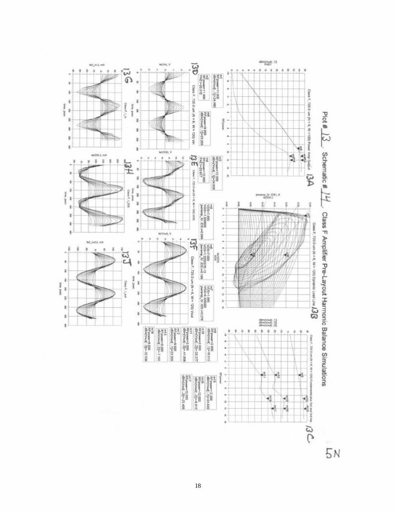
PREDICTED PERFORMANCE -- S-Parameter simulations for pre-layout design are shown in Plot #12 on page 5M with corresponding Schematic #13 on page 6N. From Plot #12E, given stated VSWR requirement of < 1.5:1 (Return Loss < -14.0 dB), resulting bandwidth > 725.0 MHz. Mu-parameters in Plot #12D show this Class-F amplifier is unconditionally stable over the bandwidth. While Plot #12B show forward gain (S21), or the small signal gain, to be >12.0 over the bandwidth as well. Parameter goal not attained during simulations was the gain ripple requirement of ±0.5 dB Max, and is discussed in: “7. CONCLUSIONS & RECOMMENDATIONS.” Harmonic balance simulations on pre-layout design, Plot #13A on page 5N with corresponding Schematic #14 on page 6P, show a 1.0 dB compression point > 24.41 dBm with a PAE of 20.51 % for an input power level of 11.0 dBm. Highest PAE was 20.82 % at an output power level of 24.64 dBm for an input power level of 12.0 dBm. Plot #13B shows dynamic load line to be Class-F. Plot #13C shows fundamental output power level along with output power levels for its 2nd and 3rd harmonics. Plots #13D - #13J are plots of currents and voltages at the input (Vin, I_in), post-amplifier drain (VDS, IDS), and on the output (Vout, I_out). Specifically, Plot #13E shows a slight flattening of voltage waveform due to the 3rd harmonic, and Plot #13H shows a slight flattening of the current sinusoid waveform due to the 2nd harmonic Final layout S-parameter simulations are shown in Plot #14, on page 5P. Schematic #4 on page 6D shows final layout schematic used for S-parameter simulations. Plot #14E gives S11 and S22 results. Aside from attaining a VSWR < 1.5:1 (Return Loss < -14.0 dB) across the band for S11 and S22, there is some distortion present on S22. Plot 14D of mu-parameters does show this amplifier unconditionally stable across the bandwidth. Plot #14B has small signal gain (S21) >12.0 dB across the required bandwidth. Final layout harmonic balance simulations are shown in Plot #15, on page 5Q. Schematic #4 on page 6D shows final layout schematic used for harmonic balance simulations. Plot #15A shows, for an input power level of 12.0 dBm, an output 1.0 dB compression point of 25.26 dBm with a PAE of 23.82 %. Highest PAE was 24.12 % for an input power level of 13.0 dBm and an output power level of 25.38 dBm. Plot #15B shows dynamic load line to be Class-F. Plot #15C has output power levels for the fundamental as well as those for its 2nd and 3rd harmonics. Plots #15D - #15J are voltage and current waveforms for the input (Vin, I_in), post-amplifier drain (VDS, IDS), and the output (Vout, I_out). Plot #51E shows a slight flattening of the VDS voltage waveform due to the 3rd harmonic, and Plot #15H shows a slightly flattened sinusoid IDS current waveform due to the 2nd harmonic.

5
3. SIMULATION PLOTS Simulation plots used in all discussions follow. Numbering for each simulation plot and its respective schematic is given in the upper left-hand corner.
6
7

8

9
10

11

12

13
14
15

16

17
18

19

20

21

22

23
4. SCHEMATIC DIAGRAMS
Schematics used in all discussions follow. Numbering for each schematic and its respective plot(s) is shown in the upper left-hand corner. A simplified schematic of the final layout is shown in Schematic #1 on page 6A. There are no corresponding plot(s) since this simplified schematic was not used in S-parameter or harmonic balance simulations.

24
25

26

27

28

29

30

31

32

33

34

35

36

37

38
39

40

41

42
5. DC ANALYSIS
SIMPLIFIED DC SCHEMATIC (No microstrip or inductors) – Schematic #15 on page 6Q is a “simplified” final layout schematic in-which all inductors were shorted. This, to see if any DC shorts existed but had not been previously noted. From Schematic #15, a possible problem found was a shorted C7 in the output resonant network. While this would not affect operation of this cascade Class-F power amplifier, it would affect a follow-on circuit without DC blocking on its input. No other possible problems were found. BIAS CHECK – Schematic #16 on page 6R is a “simplified” final layout schematic on which fixed DC supplies were used and a DC bias simulation was performed. Schematics #17 and #18 on pages 6S and 6T are partial close-ups from DC bias simulations for the final layout shown in Schematic #4 on page 6D. VDS drain voltages for both GFET amplifier stages were designed to be +7.0V. Comparisons between of these three schematics show losses for VDS from TriQuint inductors. DC simulations with a VDS supply voltage of 7.11 V gave a VDS of 6.96 V (loss of 0.15 V) for the post-amplifier and 6.93 V (loss of 0.18 V) for the pre-amplifier. It should be noted that the presence or absence of mlin components did change VDS drain voltages in these simulations. INTERCONNECT AND COMPONENT DC CURRENT STRESS – Referring to Schematics #16, #17 and #18 on pages 6R, 6S and 6T; simulated IDS current draw from the common VDS supply for both GFETs was approximately 112.0 mA for a supply voltage of +7.11 VDC (approximately 0.8 Watts of DC power). From class it was given that TriQuint inductors could handle 27.0 mA/ um, or a margin of 270.0 mA for 10.0 um inductor trace widths. IDS bias current drawn by the Class-A pre-amplifier was approximately 62.8 mA through L17, and IDS bias current drawn by the Class-AB post-amplifier was approximately 48.7 mA through L4. These IDS currents drawn through their respective drain circuit inductors are < 270.0 mA. From Plots #13B and #15B on pages 5N and 5Q respectively, it does not appear that this DC bias point is shifting appreciably due to the 25.0 Ohm de-Q’ing resistors, R1 and R4, on the gates of the pre- and post-amplifier GFETs shown in Schematic #1, on page 6A. The VGS supplies draw approximately 14.6 uA through L16 for the –0.5 VGS supply and 54.1 uA through L15 for the –1.5 VGS supply, or 7.3 uWatts and 81.15 uWatts respectively. Both DC bias currents drawn for respective VGS supplies are << 270.0 mA.
6. TEST PLAN
TEST EQUIPMENT LIST
2-port S-parameters tests across frequency range of 1.0 to 18.0 GHz:
1. Agilent 8510 Network Analyzer; 2. S-Parameter test set and flexible test cables; 3. 2 ea., 150.0 um pitch, G-S-G test probes; 4. 2 ea. test fixtures to hold G-S-G probes; 5. 2 ea. G-S-G test probe to SMA adapter connectors; 6. LRM calibration card; 7. Cleaning/flatness test card; 8. 4 ea. Picoprobe DC pin probes; 9. Microscope test bench with chuck to hold test die; 10. 3 ea. Variable power supplies for outputs of –0.5, -1.5 and 7.11 VDC; 11. VOM meter.

43
Power gain, 1.0 dB Compression Point, and PAE determinations at 5.5125 GHz: 1. #3 through #11 above plus a 3.0 dB or 6.0 dB SMA attenuator if power amplifier output exceeds input
power level of spectrum analyzer; 2. Agilent spectrum analyzer. 3. Agilent frequency synthesizer. PARAMETERS TO BE TESTED -- 1. VSWR, 2-port, 2. S-Parameters, 2-port, 3. Bandwidth, 3.0 dB points, 4. Small Signal Gain, 5. Power Input and Output at the 1.0 dB Compression Point, 6. Power gain, 7. “Under load” DC voltage and current measurements, 8. PAE. SIMULATION RESULTS FOR MEASUREMENT COMPARISON –
PARAMETER PRE-LAYOUT FINAL LAYOUT PAE 20.51 23.82 Output 1.0 dB Comp. Pt., dBm 24.49 25.26 Power Gain, dB 14.21 14.71 Ctr. Freq. S11, dB -22.99 -28.23 Ctr. Freq. S22, dB -23.05 -22.47 Ctr. Freq. Input VSWR 1.15:1 1.08:1 Ctr. Freq. Output VSWR 1.15:1 1.16:1 Ctr. Freq. S21 Small Signal Gain, dB 13.32 13.61 VDS, V 7.11 7.11 VGS_A (Pre-Amp), V/µA -0.5/14.6 -0.5/14.6 VGS_B (Post-Amp), V/µA -1.5/54.1 -1.5/54.1 IDS_A (Pre-Amp), mA 62.8 62.8 IDS_B (Post-Amp), mA 48.7 48.7 TEST CONFIGURATIONS -- A. For 2-port S-parameter and bandwidth tests from 1.0 to 18.0 GHz; refer to final layout Plot #16, Test Set-
Up #1, on page 5R. B. For power gain and 1.0 dB compression point tests at 5.5125 GHz; refer to final layout Plot #17, Test Set-
Up #2, on page 5S.
44
7. CONCLUSIONS & RECOMMENDATIONS
Cascade Class-F power amplifier operation and almost all stated performance specifications were obtained. The one exception was the required specification of ± 0.5 dB Max for gain flatness. Because of the output resonant network required for Class-F amplifier operation, roll-off from the low-pass filter action of this output network exceeded ± 0.5 dB Max for gain flatness. This roll-off can be seen in Plot #12B on page 5M, and again in Plot #14B on page 5P With regard to improvements in PAE, adjustments and/or changes to the matching network located between the amplifier stages could possibly reduce IDS current draw and DC power requirements from the VDS supply for both amplifier stages. Another possible change would be the use of self-biasing on the Class-A amplifier stage. Use of self-biasing on the Class-AB post-amplifier would interact with the output resonant network. These changes will be tested in future Class-F amplifier designs. Overall, this cascade Class-F amplifier design followed theory and design given in references [1, 2, 3, 4, 5, 6]. The most time consuming aspects in this design were with inter-actions experienced from adjustments made to the input matching network and the matching network between the amplifier stages. Small changes to achieve one design specification would result in major changes in another design specification. Adjustments made to the output matching and resonant network did not have such dramatic effects on circuit operation. Future designs will explore other methods for biasing and matching networks in a cascaded amplifier design.
8. REFERENCES
[1] Frederick H. Raab, “Class-F Power Amplifiers with Maximally Flat Waveforms,” IEEE Transactions on Microwave Theory and Techniques, Vol. 45, No. 11, November 1997, pp.2007-2012. [2] Chris Trask, “Class-F Amplifier Loading Networks: A Unified Design Approach,” 1999 MTT-S International Microwave Symposium Digest 99.1 (1999 Vol. 1 [MWSYM]): 351-354 Vol. 1. [3] William S. Kopp, “High Efficiency Power Amplification for Microwave and Millimeter Frequencies,” 1989 MTT-S International Microwave Symposium Digest 89.3 (1989 Vol. III [MWSYM]): 857-858. [4] Bernhard Ingruber, “Reliability and Efficiency Aspects of Harmonic-Control Amplifiers,” IEEE Microwave and Guided Wave Letters, Vol. 9, No. 11, November 1999. [5] Craig Moore and John Penn, 525.787 Microwave Monolithic Integrated Circuit (MMIC) Design, Johns Hopkins University, Class Notes and Handouts, Fall 2001. [6] Analysis and Design of Analog Integrated Circuits, Second Edition, Paul R. Gray and Robert G. Meyer Copyright 1977 and 1984, ISBN 0-471-87493-0.

An S – Band, 0.6-µm GaAs, Voltage Controlled Oscillator
Transient Startup of Layout with Interconnect
0 10 20 30 40 50 60 70 80 90 100
-1.4
-1.2
-1.0
-0.8
-0.6
-0.4
-0.2
0.0
0.2
0.4
0.6
0.8
1.0
1.2
1.4
time, nsec
TRAN
.Vou
t, V
Gary Levy & Steve Williams Johns Hopkins University
MMIC Design 525.787
12/17/01

I. Summary
An approach for the design of an S-Band Voltage Controlled Oscillator (VCO) for application in HyperLAN and ISM systems implemented in Triquint TQTRx 0.6-µm GaAs technology is presented. The VCO operates from 2596 MHz to 2893 MHz with output power ranging from 14.287 dBm to 12.259 dBm respectively. The VCO powered by a 5 Volt supply, features an on chip high Q resonator and tuning varactor controlled with a 0 to 5 Volt variable supply. The VCO has been used in the design of a frequency converter for a C-band HyperLAN simplex transceiver. II. Introduction A. Circuit Description
A simplex MMIC transceiver implemented in the Triquint TQTRx process (4 mil thick GaAs) with simulation and layout in Agilent ADS (ADS version 150) has been designed for C-Band HyperLAN wireless local area network (WLAN) and industrial, scientific, and medical (ISM) frequency applications.
The system utilizes a C-Band Up-Down Converter with a 275MHz intermediate frequency (IF) that can be down-converted to baseband with a second 275MHz local oscillator (LO). The second LO is upconverted to the C-Band in TX mode and modulation can be introduced onto the second LO or through direct frequency modulation of the VCO in the transceiver. The dual band usage VCO with high side or low side (HSLO/LSLO) injection to the mixer is specified for operation from 2712 MHz to 2813 MHz, which when doubled is between the WLAN and ISM frequencies.
Receive and transmit signals are routed by C-Band single-pole-double-throw (SPDT) switches. The receive chain consists of a cascaded low noise amplifier (LNA) and post amplifier. The transmit path employs a variable gain amplifier for level control and a driver amplifier preceding a 0.25 Watt power amplifier.
Figure 1. Chip-Set for the 5150 – 5350 MHz WLAN and 5725 – 5875 MHz ISM Bands.
2

The 5 Volt powered, 0 to 5 Volt voltage controlled oscillator, as shown in Fig. 2, operates from 2596 MHz to 2893 MHz with output power ranging from 14.287 dBm to 12.259 dBm respectively, while occupying only a 60 x 60 mil Anachip area. The VCO features a self-biased, W=50µm, N=6, TQTRx_DFET with an active current source utilizing a gate to source tied inductor for frequency dependent gain control which minimizes higher order harmonic components at the output. Common-source capacitive feedback is employed in the design to satisfy the required oscillation criteria with a series resonance applied at the gate of the VCO FET. The required output power is achieved by a W=70µm, N=8 source follower output stage.
Bia s Resista nc e
Reso na ntDC Blo c kingIso la tio n Resista nc e
Va ra c to r (Reso na ntByp a ss C a p a c ito r
Vo lta g e C o ntro lAC C o up ling
C urrentSo urc e
So urc e Fo llo w erBia s
So urc e Fo llo w er O utp ut
5V Sup p ly
Byp a ss C a p a c ito r
O utp ut Po rtDC Blo c king
G a in C o ntro l
Bia s Netw o rk
C g s
tq trx_reswR4
typ e=NiC rw=10 umR=2000 O hm
tq trx_G FETQ6
Ng =4W=75
tq trx_G FETQ 2
Ng=4W=75
tq trx_p ortP2
tq trx_ca pC 30c =10 p F
tq trx_p ortP3
tq trx_ca pC 31c =20 p F
tq trx_ca pC 8c =20 p F
tq trx_reswR2
typ e=NiC rw=10 umR=2000 O hm
tq trx_d indL25Ind =3500p H
tq trx_d indL24Ind =3500p H
tq trx_ca pC 32c =20 p F
tq trx_reswR12
typ e =NiCrw =10 umR=2400 O hm
tq trx_reswR9
typ e=NiC rw =5 umR=5000 O hm
tq trx_reswR13
typ e =NiCrw =10 umR=2400 O hm
tq trx_c a pC 27c =15 p F
tq trx_p ortP1
tq trx_DFETQ 3
Ng =8W=70
tq trx_DFETQ 4
Ng=8W=70
tq trx_ca pC 25c =20 p F
tq trx_DFETQ 5
Ng=6W=50
tq trx_d indL22Ind =2500p H
tq trx_DFETQ 1
Ng =6W=50tq trx_ca p
C29c =1 p F
tq trx_m rindL21
s=5 umw =5 uml2=200 uml1=200 umn=4.25
RR1R=28 O hm
tq trx_ca pC5c =3 p F
Figure 2. VCO Block Diagram. B. Design Philosophy
The VCO architecture is based upon small signal negative impedance theory where the active circuit is represented by the impedance,
Za = Ra+ jXa
and the load circuit as
Z1 = R1+ jX1
as shown in Fig. 3. Assuming that a steady state oscillation is occurring between the two networks then there must exist a loop current, I, that is non-zero. Using Kirchoff’s law, the total loop voltage then must be zero which yields
Za + Z1 = 0. It can therefore be observed that
Za = - Z1 (negative impedance) to ensure oscillation and hence the nomenclature of the theory and design technique. Furthermore, in small signal design, the imaginary portion of this relation is of particular interest and thus
Xa + X1 = 0.
3

The large signal operation of a FET oscillator can then be predicted from its small signal characteristics since as the signal grows to steady state, the actual change of the imaginary portion of the active circuit is small. The differential change in the active circuit impedance versus the operating point amplitude and frequency delta variations as described by Kurokawa is then,
[dRa/dA][dX1/dω] - [dR1/dω][dXa/dA] > 0
where Ra is the active device’s negative resistance, A is the steady state amplitude, and ω is the frequency. As stated earlier, the change in Xa with respect to amplitude is small and considered to be zero. However, for GaAs FET oscillators, Ra increases positively with respect to amplitude since the negative resistance of the circuit decreases in magnitude with increasing amplitude. Therefore applying these conditions, then
[dX1/dω]ω0 > 0 which implies that stable oscillations are ensured when the reactive component of the load impedance has a positive slope versus frequency, and the frequency of the oscillation corresponds to the zero crossing of the frequency axis. Additionally, it has been shown that for a series resonant oscillator that
|Ra| ~≥ 3R1 to approximate a power impedance match between the load circuit and the large signal steady state oscillations. The factor of 3 is itself a compromise based upon the experimental trade-off between start-up conditions and final oscillation frequency.
Za = Ra + jXa Zl = Rl + jXl
Active Device Load
TermZa
TermZl
Figure 3. Conditions for oscillator startup. To provide suitable output power for further amplification in a subsequent stage to achieve the output power specification, a 300µm (W=50µm, N=6) DFET (TQTRx DFET nonlinear model) was used to implement the oscillator and self-biased with a source resistor. The active current source is biased to provide ~12mA to the oscillator FET and has an inductor tied between the gate and source to effect a rudimentary form of frequency dependent gain control. This is because at higher frequencies, the inductor opens up and tends to choke off current from the oscillating FET. This was added to help reduce the higher order harmonic component of the
4

output since otherwise the oscillations become limited. Additionally, the 5 Volt supply of the current source includes a 20pF bypass capacitor.
Common-source capacitive feedback sets the frequency of oscillation as given by
Fosc ≅ [2π*Lr*(CVAR||Ci)0.5]-1
where
Ci=(Cgs*Cf)/(Cgs+Cf) and based upon start-up conditions, Cf was chosen to be 1pF.
The oscillator employs a series resonance at the gate to realize the negative resistance and was implemented as two 3500pH series inductors rather than one for ease of layout and tuning ability.
The Triquint varactor is implemented by two parallel 300µm (W=75µm, N=4) GFET’s with drain and source tied together and modeled as a parallel combination of a 0.04pF capacitor and a 5Ω resistor in series with the tuning capacitor as shown in Fig. 4. (See Tuning Range in Fig. 5.) As a tuning voltage is increased on the tied drains, the depletion regions of the FET’s are likewise increased. This causes an increase in the distance between the effective plates of the capacitor like structure and thus the capacitance decreases. A decrease in capacitance causes the oscillator to subsequently oscillate at a higher frequency with the converse true as well.
M o d e le d Eq uiva le n t
tq trx_G FETQ 6
Ng =4W=75
RR5R=5 O hm
CC 20C =(0.3+0.25*C fla g )
RR6R=5 O hm
CC 19C =(0.3+0.25*C fla g ) p F
CC 11C =.04 p F
CC 12C =.04 p Ftq trx_G FET
Q 2
Ng =4W=75
Figure 4. Varactor model. Bias Voltage (V) Tuned Capacitance (pF) 0 0.55 1 0.4 2 0.3 Figure 5. Single Varactor tuning range; 300µm (W=75µm, N=4) GFET.
The input network also includes a series 20pF DC blocking capacitor, a 2KΩ resistor for isolation, and a 20pF bypass capacitor to filter power supply noise. The oscillator FET is then AC coupled with a 20pF capacitor to a 560µm source follower output stage which provides the additional gain required for the output power specification. The source follower was implemented with a W=70µm and N=8 DFET to support the large bias current required to meet and or exceed the greater than 10dBm output power goal. It is biased with a resistor divider network at the gate and a W=70µm, N=8 DFET with gate tied to source. Additionally, the 5 Volt supply, which is applied to the resistor divider network, includes a 20pF bypass capacitor (same 5 Volt supply for the oscillator FET current source). A series 20pF capacitor was again added as a DC block at the output. The entire VCO architecture is illustrated in Fig. 2.
5

C. Trade-Offs
There were three major trade-off scenarios in the design of this VCO. The first trade-off encountered was the inability to use an inductive load in the first stage of
the VCO. This resulted from simulator convergence problems and rather than jeopardize the confidence level of the simulation results actually matching the fabricated circuit, the design was adapted to use a current source load so results could be better predicted with the simulator.
Design compromises were also made between the gain of the VCO and the contributions of harmonics at the output. The gain required to satisfy the start-up conditions was contrasted against the signal limiting occurring at the drain of the oscillator FET and at the output of the source follower stage, as signal compression resulted in an increased harmonic component in the output and decreased power efficiency.
Another compromise was made for the output match versus the power output. A smaller output device could have been used to match 50Ω since it could have been sized such that 1/gm equaled 50Ω, but the design is current limited in driving the output. More current was thus run in the source follower stage to drive the output and it was deliberately chosen to not match the output to minimize power loss and save area. III. Modeled Performance Specification Matrix VCO with on chip high Q resonator and tuning varactor. Specification Description
Specification Design Performance
Compliance
Frequency 2712 - 2813MHz 2596 - 2893 MHz Specification Achieved
Output Power >+ 5dBm 14.287 - 12.259 dBm
Specification Achieved
Output Power Goal
+10dBm 14.287 - 12.259 dBm
Goal Achieved
Control Voltage 0 – 5 Volts 0 – 5 Volts Specification Achieved
Supply Voltage +/- 5 Volts +5V Specification Achieved
Supply Voltage Goal
+5V +5V Goal Achieved
Output Impedance 50Ω (nominal) 50Ω (nominal) Specification Achieved
Size 60 x 60 mil ANACHIP
60 x 60 mil ANACHIP
Specification Achieved
Figure 6. Specification Compliance Matrix.
6

IV. Schematic Diagrams & Modeled Performance
LAYOUT WITHOUT INTERCONNECTVDC
VTUNE VOUT
Pa ramSweeSweep 2
Step =2Stop =1Sta rt=0SimInsta nceNa me[SimInsta nceNa me[SimInsta nceNa me[SimInsta nceNa me[SimInsta nceNa me[SimInsta nceNa me[1]="HSweep Var="Cfla g
PARAMETER SWEEP
Osc PorOsc 1
Ma xLoopGa inStepFundInd ex=1Step s=10NumOc ta vesZ=26V=
I_Prob eId 2
I_ProbeId 1
S_Pa raSP2
Step =Stop =2.8 GHzSta rt=2.7 GHz
S-PARAMETERS
tq trx_p orP4
Ha rmonicBa la ncHB1
Order[1]=3Freq [1]=2.75 GHz
HARMONIC BALANCE
DDC1
DC
TQTRx_IncNET
TQTRxNetlist Inc lude
VARVAR2Cflag=
EqnVar
tq trx_caC29c =1 p F
tq trx_resR5
type=NiCw=50R=16
tq trx_mriL21
s=5w=5l2=200l1=200n=4.25tq trx_svi
V2
tq trx_caC5c=3 p F
V_DSRC1Vd c =5 V
tq trx_caC31c =20 p F
tq trx_sviV1
tq trx_p orP3
tq trx_DFETQ5
Ng=6W=5tq trx_mri
L28
s=10w=10l2=230l1=230n=2.0
CC2C=(0.3+0.25*Cfla g)
RR48R=5
CC11C=.04 pF
CC19C=(0.3+0.25*Cfla g)
RR6R=5
CC12C=.04 p F
tq trx_sviV6
V_DSRC2Vd c =5 V
tq trx_porP2 tq trx_ca
C3c =10 p F
tq trx_resR4
typ e=NiCw=4R=3114
tq trx_DFETQ1
Ng=6W=5
tq trx_mriL27
s=10w=10l2=240l1=240n=4.25
tq trx_mriL26
s=10w=10l2=230l1=240n=4
tq trx_caC8c =20 p F
tq trx_resR17
typ e=NiCw=10R=500
tq trx_resR16
typ e=NiCw=10R=1000
tq trx_resR18
typ e=NiCw=10R=500
tq trx_resR46
type=NiCw=5R=1200
tq trx_resR45
type=NiCw=5R=1200
tq trx_sviV7
tq trx_caC34c =15 p F
tq trx_resR40
type=NiCw=5R=2400
tq trx_resR47
typ e=NiCw=2R=5000
tq trx_p orP7
tq trx_caC27c =20 p F
tq trx_p orP6
tq trx_sviV4
TerTerm
Z=50Num=
tq trx_p orP1
tq trx_caC25c =20 p F
tq trx_DFETQ3
Ng=8W=7
tq trx_DFETQ4
Ng=8W=7
Figure 7. Pre-Layout: VCO Schematic without Interconnect.
7
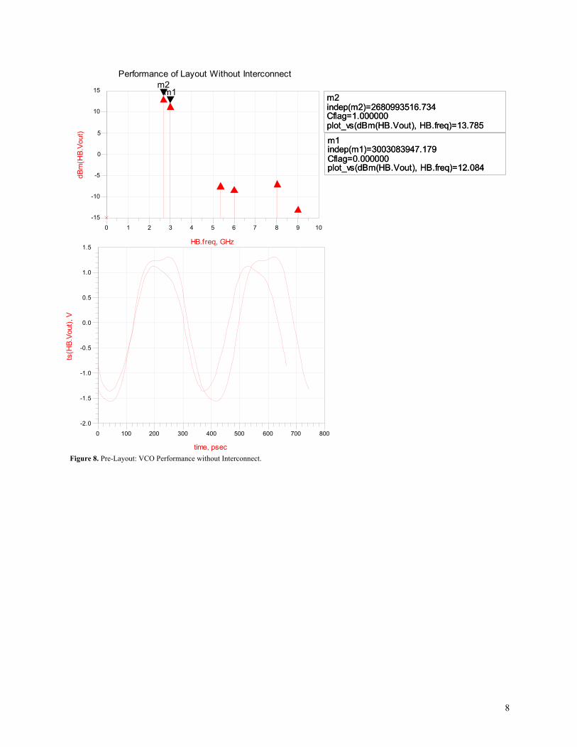
m1indep(m1)=3003083947.179Cflag=0.000000plot_vs(dBm(HB.Vout), HB.freq)=12.084
m2indep(m2)=2680993516.734Cflag=1.000000plot_vs(dBm(HB.Vout), HB.freq)=13.785m1indep(m1)=3003083947.179Cflag=0.000000plot_vs(dBm(HB.Vout), HB.freq)=12.084
m2indep(m2)=2680993516.734Cflag=1.000000plot_vs(dBm(HB.Vout), HB.freq)=13.785
0 1 2 3 4 5 6 7 8 9 10-15
-10
-5
0
5
10
15 m1m2
0 100 200 300 400 500 600 700 800-2.0
-1.5
-1.0
-0.5
0.0
0.5
1.0
1.5
Performance of Layout Without Interconnect
Figure 8. Pre-Layout: VCO Performance without Interconnect.
HB.freq, GHz
dBm
(HB.
Vout
)
time, psec
ts(H
B.Vo
ut),
V
8

SCHEMATIC OF LAYOUT WITH INTERCONNECT
VARACTOR
VTUNE
GND
GND
Cb yp ass
Rseries (R4)Rseries (R4)
Cseries
Rb ia s (R2)
Lseries (L24,L26)
Cgs_feed
Cb ias
Rb ia s (R1)
Lb ias (L21)
Ga te
Sourc e (Q1)
Dra in (Q1)
Rb ia s (R2)
Sourc e Follower Outp ut Sta ge
to
Cc oup le
Lga in_c trl (L28)
CS
Cb yp ass
VDC
GND
VOUT
to R9
to
GND
Para mSw e ep
Swee p2
Step= 2Stop= 1
Start= 0SimInstan c eN a me[ 6]=
SimInstan c eN a me[ 5]=SimInstan c eN a me[ 4]=
SimInstan c eN a me[ 3]=
SimInstan c eN a me[ 2]=SimInstan c eN a me[ 1]="HB1"
Swee pVa r="C f la g"
PARAMETER SWEEP
TermTerm 1
Z=50 Oh mNum= 1
tqt rx_resw
R40
type= NiC r
w=5 u mR=2400 Oh m
tqt rx_mlin
TL284
l=60 u m
w =10 um
tqtrx_mlin
TL288
l=241 u mw =10 um
tqtrx_mlinTL292
l=109.4 u m
w =10 um
tqt rx_mrin dL26
s=10 u mw=10 um
l2=230 um
l1=240 umn=4
tqt rx_mlinTL173
l=45 u m
w =10 um
tqtrx_DFET
Q4
Ng=8
W=70
tqt rx_mlinTL177
l=67 u mw =10 um
tqt rx_po rtP1
tqtrx_mlinTL31
l=24 u mw=10 um
tqtrx_DFET
Q1
Ng=6
W=50
tqtrx_mlinTL87
l=30 u m
w =10 um
Osc Po rtOsc 1
MaxLoo pG ainSte p=
FundIn dex= 1Steps=10
NumO c ta ves=2Z=22 Oh m
V=
tqtrx_c ornTL73
w =10 um
tqtrx_mlin
TL79
l=34.2 u m
w =10 umtqtrx_te eTL81
w3=10 u mw2=10 u m
w1=10 u m
tqtrx_mlin
TL80
l=34.2 u m
w =10 um
tqt rx_c orn
TL78
w=10 um
tqt rx_GFET
Q6
Ng=4
W=75
tqtrx_GFET
Q2
Ng=4
W=75
tqt rx_mlinTL77
l=30.5 u m
w =10 um
tqtrx_c orn
TL71
w =10 umtqt rx_mlin
TL67
l=34.2 u m
w=10 umtqtrx_c ro sTL69
w 4=10 u m
w 3=10 u mw 2=10 u m
w 1=10 u m
tqtrx_mlin
TL68
l=34.2 u m
w =10 umtqtrx_c ornTL76
w =10 um
C
C 20
C =(0.3+ 0.25*C fla g) pF
R
R48R=5 Oh m
CC 11
C =.04 pF
C
C 19
C =(0.3+0.25*Cf la g) pF
R
R6R=5 Oh m
CC 12
C =.04 pF
S_Para m
SP2
Step=Stop=2.8 G Hz
Start=2.7 G Hz
S-PARAMETERS
Ha rmonicBalan c e
HB1
Ord er[ 1]= 3
Fre q[1]= 2.75 G Hz
HARMONIC BALANC E
V_DC
SRC 2Vdc =5 V
DCDC 1
DC
TQTRx _IncNET
TQTRxNetlist Inc lude
VARVAR1
Ctune=1.0
EqnVar
VARVAR2
C flag=0
EqnVar
tqt rx_po rtP6
tqt rx_mlinTL158
l=40 u m
w =70 um
tqtrx_svia
V4
tqt rx_mlinTL107
l=20 u m
w=70 um
tqt rx_te eTL106
w3=10 u m
w2=70 u mw1=70 u m
tqtrx_mlinTL108
l=10 u mw=10 um
tqt rx_c ornTL104
w =10 um
tqt rx_mlin
TL184
l=79.2 u m
w=10 um
tqtrx_c orn
TL219w =10 um
tqt rx_DFET
Q3
Ng=8
W=70
tqtrx_mlin
TL160
l=97 u m
w =10 um
tqt rx_te e
TL161
w 3=10 u m
w 2=10 u mw 1=10 u m
tqtrx_c ornTL179
w =10 um
tqtrx_mlinTL178
l=114 u m
w =10 um
tqtrx_te e
TL182
w 3=10 u m
w 2=10 u mw 1=10 u m
tqtrx_mlinTL270
l=47 u mw =10 um
tqtrx_reswR47
type=NiC rw =2 u m
R=5000 Oh m
tqt rx_c ornTL291
w =10 um
tqtrx_c ornTL290
w =10 um
tqtrx_mlinTL181
l=30 u mw =10 um
tqtrx_c a p
C 27c=20 pF
tqtrx_mlinTL117
l=140 u mw =10 um
tqtrx_te eTL115
w 3=10 u m
w 2=10 u mw 1=10 u m
tqt rx_mlin
TL114
l=125 u m
w=10 um
tqtrx_c orn
TL113w =10 um
tqtrx_mlinTL110
l=69.6 u mw=10 um
tqtrx_c ornTL109
w =10 umtqtrx_mlin
TL96
l=158.8 u mw =10 umtqt rx_c orn
TL88w =10 um
tqtrx_mlin
TL33
l=59 u m
w =10 um
tqtrx_c orn
TL32w =10 um
tqtrx_mlinTL30
l=83.2 u mw =10 um
tqtrx_te eTL28
w 3=10 u mw 2=10 u m
w 1=10 u m
tqt rx_mlinTL29
l=25 u m
w =10 um
tqt rx_c a p
C 29c =1 pF
tqt rx_mlinTL27
l=25 u mw =10 um
tqtrx_te e
TL25
w 3=10 u m
w 2=10 u mw 1=10 u m
tqtrx_te e
TL23
w 3=10 u m
w 2=10 u mw 1=10 u m
tqtrx_mlinTL24
l=24 u mw =10 um
tqtrx_c a pC 5
c=3 pF
tqtrx_mlinTL21
l=100 u mw =10 um
tqtrx_svia
V2
tqt rx_mlin
TL13
l=92 u m
w =10 um
tqtrx_c orn
TL15
w =10 um
tqtrx_mlinTL16
l=30 u m
w =10 um
tqtrx_mrin d
L21
s=5 u m
w =5 u ml2=200 um
l1=200 umn=4.25
tqt rx_c orn
TL20w =5 u m
tqt rx_mlinTL19
l=32 u mw =10 um
tqtrx_reswR5
type=NiC r
w =50 umR=16 Oh m
tqt rx_mlinTL22
l=40 u mw =10 um
tqt rx_mlinTL43
l=15 u mw =10 um
tqt rx_c orn
TL44
w =10 um
tqt rx_mlin
TL45
l=90 u m
w=10 um
tqtrx_c orn
TL46
w =10 umtqtrx_mlinTL50
l=64 u m
w =10 um
tqt rx_c orn
TL273w =10 um
tqt rx_mlinTL49
l=15 u mw=10 um
tqt rx_c a pC30
c=10 pF
tqtrx_mlinTL52
l=25 u mw =10 umtqt rx_te e
TL51
w3=10 u m
w2=10 u m
w1=10 u m
tqtrx_mlinTL53
l=25 u mw =10 um
tqtrx_po rt
P2
tqt rx_reswR4
type= NiC r
w=4 u mR=3114 Oh m
tqtrx_c orn
TL274w =10 um
tqt rx_mlinTL276
l=50 u m
w =10 um
tqt rx_c orn
TL275w =10 um
tqt rx_te eTL5
w 3=10 u m
w 2=10 u mw 1=10 u m
tqt rx_mlinTL7
l=75 u m
w =10 um
tqtrx_mlin
TL6
l=47 u mw =10 um
tqtrx_c a p
C 8
c =20 pF
tqt rx_mlinTL8
l=20 u m
w =10 um
tqtrx_te eTL9
w 3=10 u m
w 2=10 u mw 1=10 u m
tqt rx_mlinTL10
l=40 u mw =10 um
tqt rx_mlinTL11
l=35 u mw =20 um
tqt rx_mrin d
L27
s=10 u m
w=10 uml2=240 um
l1=240 umn=4.25
tqt rx_mlin
TL26
l=25 u mw =10 um
tqtrx_reswR16
type=NiC rw =10 um
R=1000 Oh m tqtrx_c orn
TL58w =10 um
tqt rx_mlin
TL59
l=20 u mw =10 um
tqt rx_c ornTL64
w =10 um
tqt rx_resw
R17
type= NiC rw =10 um
R=500 Ohmtqt rx_c orn
TL60w =10 um
tqtrx_mlinTL61
l=20 u mw =10 um
tqtrx_c orn
TL62w =10 um
tqtrx_resw
R18
type= NiCr
w =10 um
R=500 Ohm
tqtrx_c orn
TL83w =10 um
tqt rx_mlin
TL84
l=146 u m
w =10 um
tqtrx_te eTL85
w 3=10 u m
w 2=10 u mw 1=10 u m
tqtrx_mlin
TL86
l=30 u m
w =10 um
tqtrx_svia
V6
tqtrx_mlin
TL82
l=62 u mw =10 um
tqtrx_mlinTL42
l=25 u mw =10 um
tqt rx_po rt
P4
tqtrx_mlin
TL116
l=95 u m
w =10 um
tqtrx_te eTL94
w 3=10 u m
w 2=10 u mw 1=10 u m
tqt rx_mlinTL95
l=47.8 u mw =10 um
tqtrx_mrin d
L28
s=10 u m
w =10 uml2=230 um
l1=230 umn=2.0
tqt rx_mlinTL91
l=60 u m
w =10 um
tqtrx_c orn
TL221w =10 um
tqtrx_mlin
TL90
l=30 u mw=10 um tqtrx_DFET
Q5
Ng=6
W=50
tqt rx_mlinTL168
l=70.3 u m
w=70 um
tqt rx_te e
TL170
w 3=70 u m
w 2=70 u mw 1=70 u m
tqt rx_mlin
TL271
l=229.6 u mw=70 um
tqt rx_c ornTL272
w=70 um
tqt rx_mlin
TL180
l=74 u m
w=70 um tqtrx_te eTL222
w 3=10 u mw 2=70 u m
w 1=70 u m
tqtrx_te e
TL277
w 3=10 u mw 2=10 u m
w 1=10 u mtqt rx_te e
TL278
w 3=10 u mw 2=10 u m
w 1=10 u m
tqt rx_mlin
TL289
l=20 u m
w=10 um
tqt rx_c a pC 34
c =15 pF
tqt rx_mlin
TL285
l=100 u m
w =10 um
tqtrx_c orn
TL286w=10 um
tqt rx_mlin
TL287
l=40 u m
w=10 um
tqtrx_svia
V7
tqtrx_mlin
TL293
l=20 u m
w =10 um
tqtrx_c orn
TL294w =10 um
tqt rx_mlin
TL295
l=126 u m
w=10 um
tqtrx_c ornTL297
w =10 um
tqtrx_mlin
TL296
l=27 u mw=10 um
tqtrx_po rt
P7
tqtrx_resw
R46
type= NiCr
w =5 u mR=1200 Oh m
tqtrx_c orn
TL283w =10 umtqtrx_mlin
TL282
l=51 u m
w =10 umtqtrx_c ornTL281
w =10 um
tqtrx_resw
R45
type=NiC rw=5 u m
R=1200 Oh m
tqtrx_c orn
TL280w =10 um
tqtrx_mlin
TL279
l=20 u m
w =10 um
tqtrx_te e
TL185
w 3=10 u mw 2=70 u m
w 1=70 u m
tqtrx_mlin
TL183
l=40 u m
w =70 um
tqtrx_po rtP3
V_DC
SRC1Vdc= 5 V
tqt rx_mlinTL187
l=20 u m
w =10 um
tqtrx_c orn
TL224w =10 um
tqtrx_mlin
TL188
l=20 u mw =10 um
tqtrx_c orn
TL226w =10 um
tqtrx_mlinTL190
l=20 u mw =10 um
tqtrx_c a pC 31
c=20 pF
tqtrx_mlin
TL191
l=80 u m
w =10 um
tqt rx_c orn
TL192
w =10 umtqtrx_mlin
TL193
l=25 u m
w=10 umtqtrx_svia
V1
tqtrx_mlin
TL92
l=25.8 u mw =10 um
tqt rx_mlin
TL159
l=82.2 u m
w =10 um
tqt rx_c a p
C 25c =20 pF
tqt rx_mlin
TL157
l=40 u m
w =10 um
Figure 9. Post-Layout: VCO Schematic with Interconnect.
9
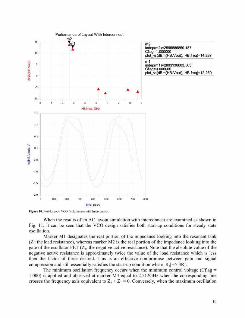
0 100 200 300 400 500 600 700 800-2.0
-1.5
-1.0
-0.5
0.0
0.5
1.0
1.5
time, psec
ts(H
B.Vo
ut),
V
m1indep(m1)=2893130603.563Cflag=0.000000plot_vs(dBm(HB.Vout), HB.freq)=12.259
m2indep(m2)=2596886850.187Cflag=1.000000plot_vs(dBm(HB.Vout), HB.freq)=14.287m1indep(m1)=2893130603.563Cflag=0.000000plot_vs(dBm(HB.Vout), HB.freq)=12.259
m2indep(m2)=2596886850.187Cflag=1.000000plot_vs(dBm(HB.Vout), HB.freq)=14.287
0 1 2 3 4 5 6 7 8 9-10
-5
0
5
10
15 m1m2
Performance of Layout With Interconnect
HB.freq, GHz
dBm
(HB.
Vout
)
Figure 10. Post-Layout: VCO Performance with Interconnect.
When the results of an AC layout simulation with interconnect are examined as shown in Fig. 11, it can be seen that the VCO design satisfies both start-up conditions for steady state oscillation. Marker M1 designates the real portion of the impedance looking into the resonant tank (Zl; the load resistance), whereas marker M2 is the real portion of the impedance looking into the gate of the oscillator FET (Za; the negative active resistance). Note that the absolute value of the negative active resistance is approximately twice the value of the load resistance which is less then the factor of three desired. This is an effective compromise between gain and signal compression and still essentially satisfies the start-up condition where |Ra| ~≥ 3R1.
The minimum oscillation frequency occurs when the minimum control voltage (Cflag = 1.000) is applied and observed at marker M3 equal to 2.512GHz when the corresponding line crosses the frequency axis equivalent to Za + Z1 = 0. Conversely, when the maximum oscillation
10

frequency is applied (Cflag = 0.000), the maximum oscillation frequency is observed at M4 equal to 2.825 GHz. Note that the deviations in oscillation frequency as compared to previous simulation results are attributed to the differences in numerical solving methods between linear AC simulations and harmonic balance simulations.
Finally, observe that the top two unlabeled traces of Fig. 11 exhibit positive slopes for the imaginary portion of the impedance’s looking into the resonant tank at both minimum and maximum control voltages (Cflag = 1.000, Cflag = 0.000) satisfying the condition where [dX1/dω]ω0 > 0 is required.
m2freq=2.825GHzCflag=1.000000real(Z(2,2))=-25.224
m1freq=2.826GHzCflag=0.000000real(Z(3,3))=13.152
m3freq=2.512GHzCflag=1.000000imag(Z(3,3))+imag(Z(2,2))=-0.07m4freq=2.825GHzCflag=0.000000imag(Z(3,3))+imag(Z(2,2))=-0.07
m2freq=2.825GHzCflag=1.000000real(Z(2,2))=-25.224
m1freq=2.826GHzCflag=0.000000real(Z(3,3))=13.152
m3freq=2.512GHzCflag=1.000000imag(Z(3,3))+imag(Z(2,2))=-0.07m4freq=2.825GHzCflag=0.000000imag(Z(3,3))+imag(Z(2,2))=-0.07
2.50 2.55 2.60 2.65 2.70 2.75 2.80 2.85 2.90 2.95 3.00-40
-20
0
20
40
60
80
100
freq, GHz
real
(Z(2
,2))
m2
real
(Z(3
,3))
m1
imag
(Z(3
,3))
+im
ag(Z
(2,2
))
m3 m4
imag
(Z(3
,3))
AC Analysis of Layout With Interconnect
Figure 11. Post-Layout: AC Analysis of VCO with Interconnect.
11

0 10 20 30 40 50 60 70 80 90 100
-1.4
-1.2
-1.0
-0.8
-0.6
-0.4
-0.2
0.0
0.2
0.4
0.6
0.8
1.0
1.2
1.4Transient Startup of Layout with Interconnect
time, nsec
TRAN
.Vou
t, V
Figure 12. Post-Layout: Transient Analysis of VCO with Interconnect.
12

V. DC Analysis A. Simplified DC Schematic
The original schematic without interconnect was edited such that all inductors were replaced with shorts and the capacitors opened, given that at DC, the frequency is zero. This is done to check for any inadvertent biasing shorts, shorting of the supplies, and to follow the biasing path.
O PEN
Sim p lified DC
O PEN
O PEN
O PEN
O PEN
O PEN
O PENAC C o up ling
O PEN
Bia s Resista nc e
Reso na ntDC Blo c kingIso la tio n Resista nc e
Va ra c to r (Reso na n t
Byp a ss C a p a c ito r
Vo lta g e C o ntro l
C urren tSo urc e
So urc e Fo llo w erBia s
So urc e Fo llo w er O utp ut
5V Sup p ly
Byp a ss C a p a c ito r
O utp ut Po rtDC Blo c king
G a in C o ntro l
Bia s Ne tw o rk
C g s
tq trx_reswR4
typ e =NiC rw =10 umR=2000 O hm
tq trx_G FETQ 6
Ng =4W=75
tq trx_G FETQ 2
Ng=4W=75
tq trx_p o rtP2
tq trx_c a pC 30c =10 p F
tq trx_p ortP3
tq trx_ca pC 31c =20 p F
tq trx_ca pC 8c =20 p F
tq trx_reswR2
typ e=NiC rw =10 umR=2000 O hm
tq trx_ca pC 32c =20 p F
tq trx_reswR12
typ e=NiC rw =10 umR=2400 O hm
tq trx_reswR9
typ e=NiC rw =5 umR=5000 O hm
tq trx_reswR13
typ e=NiC rw =10 umR=2400 O hm
tq trx_ca pC 27c =15 p F
tq trx_p o rtP1
tq trx_DFETQ 3
Ng =8W=70
tq trx_DFETQ4
Ng =8W=70
tq trx_c a pC 25c =20 p F
tq trx_DFETQ 5
Ng=6W=50
tq trx_DFETQ 1
Ng=6W=50tq trx_ca p
C 29c =1 p F
RR1R=28 O hm
tq trx_c a pC 5c =3 p F
Figure 13. Simplified DC schematic of VCO. B. Bias Check FET (tqtrx_DFET)
Function VGS (mV) VDS (Volts) IDS (mA)
Q1 VCO FET -203 4.5 12.8 Q5 VCO FET
Current Source 0 0.290 12.8
Q4 Source Follower 0 2.5 40.9 Q3 Source Follower
Current Source 0 2.5 40.9
Figure 14. DC Operating Points. C. Interconnect and Component DC Current Stress
The VCO was simulated at DC and the current and voltage values at each of the circuit nodes were annotated upon the schematic. Based upon the TQTRx process design rules with respect to FET current handling, passive component current handling, and metal current density, no current thresholds appear to be violated.
13
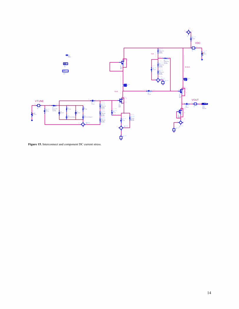
1mA
12mA
40.8mA
VTUNE
VDC
VOUT
CC20C=(0.3+0 .25*Cflag) pF
RR48R=5 Ohm
CC11C=.04 pF
CC19C=(0.3+0 .25*Cflag ) pF
RR6R=5 Ohm
CC12C=.04 pF
tqtrx _s v iaV6
V_DCSRC2Vdc =5 V
tqtrx _po rtP2
tqtrx _c apC30c =10 pF
tqtrx _ res wR4
ty pe=NiCrw=4 umR=3114 Ohm
tqtrx _c apC8c =20 pF
tq trx _ res wR17
ty pe=NiCrw=10 umR=500 Ohm
tq trx _ res wR16
ty pe=NiCrw=10 umR=1000 Ohm
tq trx _ res wR18
ty pe=NiCrw=10 umR=500 Ohm
tqtrx _c apC29c =1 pF
I_ProbeId2
I_ProbeId1
tqtrx _po rtP4
DCDC1
DC
TQTRx _IncNET
TQTRxNetl i s t Inc lude
VARVAR2Cflag=0
EqnVar
tqtrx _res wR5
ty pe=NiCrw=50 umR=16 Ohm
tqtrx _s v iaV2
tqtrx _c apC5c =3 pF
V_DCSRC1Vdc =5 V
tqtrx _c apC31c =20 pF
tq trx _s v iaV1
tqtrx _portP3
tq trx _DFETQ5
Ng=6W=50
tqtrx _DFETQ1
Ng=6W=50
tqtrx _res wR46
ty pe=NiCrw=5 umR=1200 Ohm
tqtrx _res wR45
ty pe=NiCrw=5 umR=1200 Ohm
tq trx _s v iaV7
tqtrx _c apC34c =15 pF
tqtrx _res wR40
ty pe=NiCrw=5 umR=2400 Ohm
tqtrx _res wR47
ty pe=NiCrw=2 umR=5000 Ohm
tqtrx _po rtP7
tqtrx _c apC27c =20 pF
tq trx _portP6
tqtrx _s v iaV4
TermTerm 1
Z=50 OhmNum =1
tqtrx _po rtP1
tqtrx _c apC25c =20 pF
tq trx _DFETQ3
Ng=8W=70
tqtrx _DFETQ4
Ng=8W=70
Figure 15. Interconnect and component DC current stress.
14

VI. Layout
Figure 16. VCO layout.
15

VII. Test Plan
The bias (5 Volt supply) and frequency control (0-5 Volt variable supply) is applied to the designated pads on the layout with needle probes.
See Fig. 14 for the respective DC bias points for each transistor. Total DC current consumed by the VCO is ~55mA (the sum of each of the transistor bias currents at DC and the resistor ladder.)
The RF output should be extracted with ground-signal-ground (GSG) probes to a spectrum analyzer. The expected signal at the output should be a ~2 Volt peak to peak sinusoid, oscillating between 2596 MHz to 2893 MHz with corresponding power of 14.287 dBm to 12.259 dBm. VIII. Conclusion & Recommendations
Given more time, a greater effort would have been spent to develop a more robust and innovative adaptive bias technique to limit the harmonic contribution to the output signal at the oscillation frequencies of interest while still maintaining a high gain at DC for startup.
Finally, given the design constraints for a HyperLan and or ISM frequency system, the VCO based upon schematic simulation results, layout simulation results, and peer and expert review, should both meet and or exceed each of the given VCO specifications. IX. Acknowledgements A special thanks is given to Craig Moore and John Penn of Johns Hopkins University for their assistance as well as to the class of 525.787 for their peer review. The use of ADS version 150 and tool and design kit support by Gary Wray of Agilent is also greatly appreciated. The authors would also like to graciously thank Triquint for process related information and the fabrication of this design in the TQTRx GaAs process.
16
X. References J. Andrews, T. Holden, K. Lee, A. Podell, 2.5-6.0GHz Broadband GaAs MMIC VCO, IEEE MTT-S Digest, 1988. W. Baumberger, M. Schmatz, A GaAs Single Chip 2.4GHz PLL Frequency Multiplier, IEEE Microwave & Millimeter-Wave Monolithic Circuits Symposium 1996. H. Chen, A GaAs MESFET MMIC C Band Voltage Controlled Oscillator, Johns Hopkins University Course 525.787, Fall 2000. F. Ellinger, U. Lott, w. Bachtold, Design of a Low-Supply-Voltage High Efficiency Class-E Voltage-Controlled MMIC Oscillator at C-Band, IEEE Transactions on Microwave Theory & Techniques, Vol. 49, No. 1, January 2001. gEE-CAD User’s Guide, Johns Hopkins University Courses 525.774 –775, Sept. 2000. C. Lee, S. Han, B. Matinpour, J. Laskar, A Low Phase Noise X-Band MMIC GaAs MESFET VCO, IEEE Microwave & Guided Wave Letters, Vol. 10, No. 8, August 2000. J. Shealy, J. J. Shealy, Low-Phase Noise AlGaN/GaN FET-Based Voltage Controlled Oscillators (VCOs), IEEE Microwave & Wireless Component Letters, Vol. 11, No. 6, June 2001. D. Warren, J. Golio, W. Seely, Large and Small Signal Oscillator Analysis, Microwave Journal, May 1989.
17
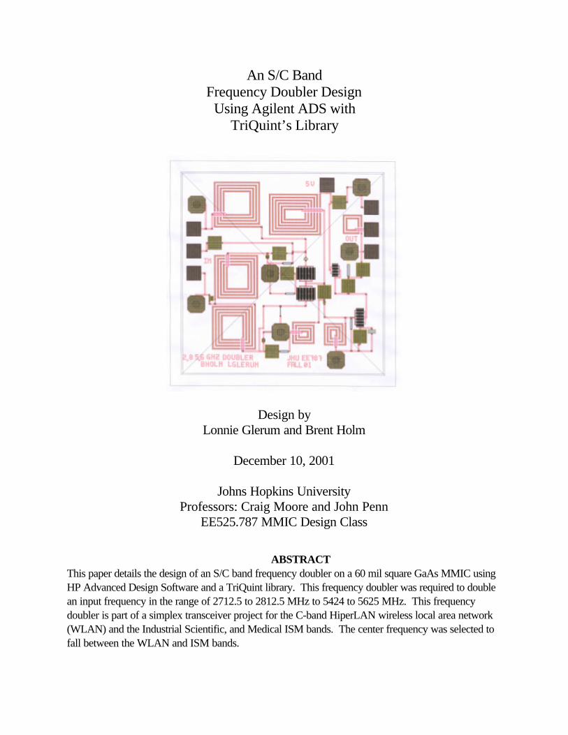
An S/C BandFrequency Doubler Design
Using Agilent ADS withTriQuint’s Library
Design byLonnie Glerum and Brent Holm
December 10, 2001
Johns Hopkins UniversityProfessors: Craig Moore and John Penn
EE525.787 MMIC Design Class
ABSTRACTThis paper details the design of an S/C band frequency doubler on a 60 mil square GaAs MMIC usingHP Advanced Design Software and a TriQuint library. This frequency doubler was required to doublean input frequency in the range of 2712.5 to 2812.5 MHz to 5424 to 5625 MHz. This frequencydoubler is part of a simplex transceiver project for the C-band HiperLAN wireless local area network(WLAN) and the Industrial Scientific, and Medical ISM bands. The center frequency was selected tofall between the WLAN and ISM bands.

Page 1 of 10
1 INTRODUCTION
1.1 Circuit Description
This MMIC frequency doubler consists of a differential pair of GFET’s, a 180 degree phase shift
network, and general purpose 2nd stage amplifier. The inputs of the differential pair are fed 180 degrees
out of phase by a lumped element 180 degree phase shift network. Each transistor in the differential
pair is biased class B that is to have a 50% conduction angle. The output appears as a full wave
rectified version of the input, each transistor contributing every other “hump” in the output. Because of
the symmetry of the output waveform (it is ideally even symmetric and half-wave even symmetric), it
contains no odd harmonics. Therefore, the fundamental and third harmonics normally present in a
nonlinear element doubler have been removed by symmetry. A second stage general purpose amplifier
provides approximately 6 dB of gain to account for the conversion loss in the differential pair of GFETs.
1.2 Design Philosophy
The first step to designing this frequency doubler was to determine if the differential GFET pair
would give the desired 2nd harmonic output while rejecting the 3rd harmonic and fundamental
frequencies. A simple schematic consisting of a GFET differential pair with biasing power supplies and
an ideal 180 degree transmission line was created and simulated with HP ADS. TriQuint 300 um
GFET devices were selected initially since the 300 um device is TriQuint’s standard device. A gate to
source voltage (Vgs) of –2 V that is near the threshold voltage (see figure below) provided good results.
The next step in the design process was to create a 180 degree phase shift network from ideal
lumped elements, since the operating frequency is too low for any practical transmission line elements.
Page 2 of 10
To minimize the number of inductors required for a 180 degree lumped element, a double-Pi (two
cascaded 90 degree lowpass networks) network was designed for a 50 ohm impedance. When the
ideal 180 degree transmission line was replaced with the double-Pi 180 degree lumped element
network the frequency doubler still provided good results.
The next step in the design process was replacing the ideal power supply biasing at the gate and
drain with a self-bias scheme using a single 5 volt power supply. A large 10 pF shunt capacitor at the
power supply and large series inductor of approximately 6000 pH provided adequate RF to DC
isolation. Each gate of the differential pair was provided an approximate 0 Volt dc bias through a large
resistor to ground. A shared 180 ohm source resistor bypassed with a large 10 pF shunt capacitor
provided approximately minus 2.0 volts DC for Vgs.
Once proper biasing was obtained, the input matching network (IMN) and output matching
networks (OMN) were designed. With the IMN and OMN networks added, the doubler contained a
potentially unstable region at approximately 3.4 GHz. This oscillation was traced to a parallel resonance
in the double-Pi 180 degree lumped element network. Professor Craig Moore suggested changing the
double-Pi 180 degree lumped element network to a 100 ohm impedance and placing 100 ohm resistors
at the gates of the differential pair to stabilize the circuit. This change worked very nicely and had the
added benefit of a more broadband match at the IMN and OMN when the networks were retuned.
All ideal elements were replaced with TriQuint elements and the circuit was resimulated. This
action degraded the performance of the frequency doubler. It was found that the resistive losses in the
TriQuint discrete inductors caused a voltage difference between the right and left gates of the differential
pair. To account for the resistive losses in the inductor, an 18 ohm series resistor was added at the left
gate of the differential pair. The IMN and OMN were also tuned to optimize performance.
At this point in the design process, a rough layout design was performed to ensure that the current
circuit would fit on a 60 mil square GaAs MMIC with some room to spare for a 2nd stage amplifier.
The circuit layout left about 1/5 of the area for a 2nd stage amplifier which was needed to provide an
additional 6 dB gain to reach the goal conversion loss of 0 dB. To fit a second stage amplifier in this
area, an active bias network (a half-sized FET with its gate and source connected to create a current
source) was selected for the second stage. Furthermore, the IMN and OMN’s were kept physically

Page 3 of 10
small by using 200 ohm shunt resistors at the input and output, and by choosing topologies that
minimized the amount of inductance required.
1.3 Trade-Offs
The most significant and earliest tradeoff made was the choice of circuit architecture. By
using a pair of GFET's driven out of phase for the doubler, it was possible to save a filter that would
have been required to block the fundamental and third harmonic created by a more straightforward
diode-connected-FET single non-linearity design. Of course, this choice meant it was necessary to
construct a phase shift network. It wasn't possible to build both and do a comparison, but the dual
transistor approach seemed more novel and elegant, so it was the one chosen. During the layout
process, there were numerous small tradeoffs. Individual inductors only come in discrete sizes, so every
time our design called for one, we had to add some microstrip line to tune the inductance. And every
time we added microstrip line to physically connect things, we had to account for that additional
inductance somewhere else. The post-amplifier circuit was designed to be small, not for high
performance. Most notably, it has large stabilizing shunt loads on its input and output that made the
circuit easier to match to 50 ohms without using large components, especially inductors. It also uses an
active load for the bias circuit, which also saves space over that of an inductor used as an RF choke.
2 MODELED PERFORMANCE
2.1 Specifications Compliance Matrix
Characteristic Specifications Pre-Layout Results Final Layout ResultsInput Frequency Range 2712.5 – 2812.5 MHz 2712.5 – 2812.5 MHz 2712.5 – 2812.5 MHzOutput Frequency Range 5425 – 5625 MHz 5425 – 5625 MHz 5425 – 5625 MHzConversion Loss 3 dB max 5.4 dB <0 dBSpurious Fundamental Output 16dBc min, 25 dBc goal 32.8 dBc 39.8 dBcSpurious 3rd Order Output 20dBc min, 30 dBc goal 39.8 dBc 35.9 dBcInput VSWR, 50 Ohms 2.5:1 max, 1.5:1 goal 1.19 max 1.28 maxOutput VSWR, 50 Ohms 2.5:1 max, 1.5:1 goal 1.34 max 1.13 maxSupply Voltage +/- 5 V, +5 V only goal +5 V only +5 V onlySize 60 x 60 mil ANACHIP 60 x 60 mil ANACHIP 60 x 60 mil ANACHIP

Page 4 of 10
2.2 Predicted Performance
Figures 1- 3 show the predicted performance of the final layout for the 2.7 - 2.8 GHz frequency
doubler.
2.2.1 Output Harmonic Content vs. RF Power In
Figure 1 details the expected output spectrum of the frequency doubler over a swept RF input level.
Marker m2 is the desired doubler output for an input level of +10 dBm. The final layout predicts a
conversion gain of approximately 2 dB, and suppression of the fundamental and 3rd order products that
exceeds the design goals.
Figure 1

Page 5 of 10
2.2.2 Input and Output Waveforms
Figure 2 shows the time domain representation of the input and output waveforms of the frequency
doubler.
Figure 2

Page 6 of 10
2.2.3 Input VSWR and Output VSWR
Figure 3 shows the predicted VSWR performance of the input and output ports.
Figure 3

Page 7 of 10
3 SCHEMATIC DIAGRAMS
3.1 Simplified Schematic
The schematic below has been simplified by removing all routing microstrip lines (bends tees and shortMLINs), which did not significantly affect the simulated results.
4 DC ANALYSIS
4.1 DC Schematic
The DC schematic below has been simplified further by replacing inductors and microstrip lines withwires.

Page 8 of 10
4.2 Bias Check
A bias check was performed on the simplified schematic to ensure that there was no inadvertent DC
shorts to ground and that the circuit was biased properly. All biasing was correct, however it was
discovered that blocking caps at the input and output ports were inadvertently left out of the schematic.
4.3 Interconnect and Component DC Current Stress
In performing the interconnect and component DC current stress analysis, instructors John Penn and
Craig Moore discovered that resistor R6 located in series with drain of the output stage amplifier did not
have sufficient width to support the current. All other components were satisfactory.
4.4 Final Layout

Page 9 of 10
5 TEST PLAN
RF InRF Out
SpectrumAnalyzer
SignalGenerator2.7 GHz+10dBm
RF Probe Station
MMICDoubler
DC Power Supply
+5V~55mA
Test Equipment Required:• 1 Glerum/Holm GaAs MMIC Doubler• 1 RF Signal Generator, 2.7-2.8GHz, +5-15dBm output, (+10dBm minimum)• 1 Spectrum Analyzer, 1-12GHz (6 GHz minimum). Power out of device could exceed
+15dBm, use attenuator if necessary.• 1 DC Power Supply (+5Vdc, 100mA) with DC milliammeter• 1 Needle Probe for DC bias• 2 RF Ground-Signal-Ground Probes
Test Plan:
1. Visual Inspection. Verify the chip’s identity against the paper printout and check for obviousphysical defects. Look for missing elements, inverted components, and chips and cracks.
2. Bias Current Test. With power supply off and set to 0V, connect the supply leads to theMMIC doubler chip. Turn supply on and slowly raise the voltage toward +5V. Monitor thecurrent and shut the supply off if it goes above 70mA. (55mA is predicted draw.) Record theactual current draw here ______mA.
3. RF Connections . Install MMIC in RF test fixture with its text oriented right side up. Connectthe RF input on the left and the RF output on the right.
4. Functional Test. Turn on the signal generator and set it to +10dBm, 2.7GHz. Verify thatthere is a 2Fo component on the spectrum analyzer within ~6dB of the input level.
5. Swept Power Test. Sweep the input power from +5dBm to +15dBm in 1dB steps and notethe power in the frequency doubled term for each step. Also note the power in thefundamental, third, and fourth harmonics. Graph the results and compare them to theoretical.
6. Input and Output Match. If time permits, use a network analyzer to check the inputimpedance around 2.7-2.8GHz and the output match around 5.4-5.6GHz. Compare totheoretical.

Page 10 of 10
6 CONCLUSION AND RECOMMENDATIONS
Using a differential pair of GFETs in class B operation proved to be good topology for a frequency
doubler when proper balance was maintained. Careful selection of the bias point near cutoff is required
such that each transistor only conducts for 180 degrees of the input wave. The double-Pi 180 degree
lumped element network had the potential to cause instability in the differential pair when it was
originally designed for an impedance of 50 ohms. By designing the double-Pi 180 degree network for a
100 ohm impedance and placing 100 ohm resistors to ground at each end of the network, the circuit
was made stable. Further tweaking of the first and last series capacitors in the double-Pi 180 degree
network allowed tuning to ensure a 180 degree phase shift.
When laying the frequency doubler schematic out using Agilent ADS several common mistakes
could have been avoided. It is recommended to carefully consider placement of inductors. Try to allow
for at least 50 mils of space between an inductor and other microstrip lines, vias, or other inductors.
Also try to keep a spacing of 60 mils between capacitors and vias. The instructors caught most of the
errors in the initial frequency doubler layout using a Design Rule Check (DRC) program.