monolithic microwave integrated circuits (mmic) broadband ... · (jhu) mmic design course, taught...
TRANSCRIPT
Monolithic Microwave Integrated Circuits (MMIC)
Broadband Power Amplifiers (Part 2)
by John E. Penn
ARL-TN-0556 July 2013
Approved for public release; distribution unlimited.

NOTICES
Disclaimers
The findings in this report are not to be construed as an official Department of the Army position
unless so designated by other authorized documents.
Citation of manufacturer’s or trade names does not constitute an official endorsement or
approval of the use thereof.
Destroy this report when it is no longer needed. Do not return it to the originator.
Army Research Laboratory Adelphi, MD 20783-1197
ARL-TN-0556 July 2013
Monolithic Microwave Integrated Circuits (MMIC)
Broadband Power Amplifiers (Part 2)
John E. Penn
Sensors and Electron Devices Directorate, ARL
Approved for public release; distribution unlimited.

ii
REPORT DOCUMENTATION PAGE Form Approved
OMB No. 0704-0188 Public reporting burden for this collection of information is estimated to average 1 hour per response, including the time for reviewing instructions, searching existing data sources, gathering and maintaining the
data needed, and completing and reviewing the collection information. Send comments regarding this burden estimate or any other aspect of this collection of information, including suggestions for reducing the
burden, to Department of Defense, Washington Headquarters Services, Directorate for Information Operations and Reports (0704-0188), 1215 Jefferson Davis Highway, Suite 1204, Arlington, VA 22202-4302.
Respondents should be aware that notwithstanding any other provision of law, no person shall be subject to any penalty for failing to comply with a collection of information if it does not display a currently
valid OMB control number.
PLEASE DO NOT RETURN YOUR FORM TO THE ABOVE ADDRESS.
1. REPORT DATE (DD-MM-YYYY)
July 2013
2. REPORT TYPE
Final
3. DATES COVERED (From - To)
4. TITLE AND SUBTITLE
Monolithic Microwave Integrated Circuits (MMIC) Broadband Power
Amplifiers (Part 2)
5a. CONTRACT NUMBER
5b. GRANT NUMBER
5c. PROGRAM ELEMENT NUMBER
6. AUTHOR(S)
John E. Penn
5d. PROJECT NUMBER
5e. TASK NUMBER
5f. WORK UNIT NUMBER
7. PERFORMING ORGANIZATION NAME(S) AND ADDRESS(ES)
U.S. Army Research Laboratory
ATTN: RDRL-SER-E
2800 Powder Mill Road
Adelphi, MD 20783-1197
8. PERFORMING ORGANIZATION REPORT NUMBER
ARL-TN-0556
9. SPONSORING/MONITORING AGENCY NAME(S) AND ADDRESS(ES)
10. SPONSOR/MONITOR'S ACRONYM(S)
11. SPONSOR/MONITOR'S REPORT NUMBER(S)
12. DISTRIBUTION/AVAILABILITY STATEMENT
Approved for public release; distribution unlimited.
13. SUPPLEMENTARY NOTES
14. ABSTRACT
A broadband amplifier design approach for microwave monolithic integrated circuits (MMICs) was previously documented in
a technical report, ARL-TR-6278, Monolithic Microwave Integrated Circuits (MMIC) Broadband Power Amplifiers,
December 2012. The three amplifier designs previously fabricated and tested as part of the fall 2011 Johns Hopkins University
(JHU) MMIC Design Course, taught by the author, covered 2–6, 5–11, and 28 GHz. Since there was extra space available in
the fall 2012 JHU MMIC Design Course fabrication, two additional amplifiers were designed, fabricated, and tested following
the same design approach. This follow-up technical note documents the two recent amplifier designs, one was designed for
1–5 GHz operation and the second for 10–19 GHz operation.
15. SUBJECT TERMS
MMIC, broadband, power amplifier, GaAs
16. SECURITY CLASSIFICATION OF:
17. LIMITATION OF
ABSTRACT
UU
18. NUMBER OF
PAGES
20
19a. NAME OF RESPONSIBLE PERSON
John E. Penn a. REPORT
Unclassified
b. ABSTRACT
Unclassified
c. THIS PAGE
Unclassified
19b. TELEPHONE NUMBER (Include area code)
(301) 394-0423
Standard Form 298 (Rev. 8/98)
Prescribed by ANSI Std. Z39.18

iii
Contents
List of Figures iv
List of Tables iv
Acknowledgments v
1. Introduction 1
2. Design Approach 1
3. A 1‒5 GHz Broadband Power Amplifier 1
4. A 10‒19 GHz Broadband Power Amplifier 6
5. Conclusion 10
List of Symbols, Abbreviations, and Acronyms 11
Distribution List 12

iv
List of Figures
Figure 1. Layout plot of the 1–5 GHz power amplifier (~0.9 x 0.9 mm). .......................................2
Figure 2. A 2-GHz load-pull simulation of output power (Pcomp-6 x 65 µm PHEMT). ..............2
Figure 3. A 2-GHz load-pull simulation of PAE (6 x 65 µm PHEMT). .........................................3
Figure 4. MMIC 1–5 GHz broadband power amplifier linear simulations versus measured (solid). ........................................................................................................................................4
Figure 5. MMIC 1–5 GHz output power and PAE performance simulation (1, 2, 3, and 4 GHz). ..........................................................................................................................................4
Figure 6. Layout plot of the 10–19 GHz power amplifier (~1.1 x 0.5 mm). ...................................6
Figure 7. A 16-GHz load-pull simulation of output power (Pcomp-6 x 50 µm PHEMT). ............7
Figure 8. A 16-GHz load-pull simulation of PAE (6 x 50 µm PHEMT). .......................................7
Figure 9. MMIC 10–19 GHz broadband power amplifier linear simulations vs. measured (solid). ........................................................................................................................................8
Figure 10. MMIC 10–19 GHz output power and PAE performance simulation (14, 16, and 18 GHz). ..........................................................................................................................................9
List of Tables
Table 1. Power performance for the 1–5 GHz broadband amplifier. ..............................................5
Table 2. Power performance for the 10–19 GHz broadband amplifier. ..........................................9

v
Acknowledgments
Once again, I would like to acknowledge the support of the U.S. Army Research Laboratory
(ARL) in supporting my part-time passion of teaching the Johns Hopkins University (JHU)
Monolithic Microwave Integrated Circuit (MMIC) Design Course, as well as TriQuint
Semiconductor for fabricating designs for JHU students since 1989. Software support for these
JHU designs is provided by Applied Wave Research (AWR), Agilent, Inc., and Sonnet Software.

vi
INTENTIONALLY LEFT BLANK.

1
1. Introduction
Amplifier design is a tradeoff of gain, bandwidth, noise performance, power performance,
efficiency, stability, and impedance match. The following broadband amplifier design approach
emphasizes good output power and efficiency, with broadband gain and match. Previously, three
amplifier designs were fabricated in TriQuint Semiconductor’s 0.13-µm TQP13 gallium arsenide
(GaAs) process and tested as part of the fall 2011 Johns Hopkins University (JHU) Monolithic
Microwave Integrated Circuit (MMIC) Design Course, taught by the author, covering 2–6, 5–11,
and 28 GHz. Since there was extra space available in the fall 2012 JHU MMIC Design Course
fabrication, two additional amplifiers using the TQP13 process were designed, fabricated, and
tested following the same broadband power amplifier design approach. One amplifier was
designed for a lower band of 1–5 GHz operation, while the second was designed for 10–19 GHz
operation.
2. Design Approach
The design approach follows the double “Q” output matching described in ARL-TR-62781. After
designing the broadband output match for good efficiency and bandwidth, a simple high-pass,
low-pass (HP/LP) input match is used to achieve good return loss across the full bandwidth,
which is constrained by the transistor’s parasitics. Simulations using Microwave Office (MWO)
with the TriQuint TQP13 0.13-µm pseudomorphic high electron mobility transistor (PHEMT)
process are shown for each of the two amplifier designs.
3. A 1‒5 GHz Broadband Power Amplifier
The broadband design approach was used for an amplifier centered at 2 GHz. Figure 1 shows the
layout of the 1–5 GHz amplifier. A simple low-pass input match consisting of a shunt capacitor
and series inductor provided a compromise with fair input return loss and broadband gain. This
design used a 6 x 65 µm PHEMT, instead of the standard 6 x 50 µm PHEMT used in the other
broadband designs. A compromise was struck between the best output power and best efficiency
using the nonlinear model for load-pull equivalent simulations (figures 2 and 3). Best output
match was chosen as 65 Ω in parallel with 184 fF, for a “Q” of 0.2. Using the two load contour
simulations, this output match should yield 20.8 dBm of output power at 61% power-added
1Penn, J. Monolithic Microwave Integrated Circuits (MMIC) Broadband Power Amplifiers; ARL-TR-6278; U.S. Army
Research Laboratory: Adelphi, MD, December 2012.

2
efficiency (PAE) (2 GHz). This estimate uses the TQP13 TOM4 nonlinear model biased at 4 V
DC with ideal lossless matching elements.
Figure 1. Layout plot of the 1–5 GHz power amplifier (~0.9 x 0.9 mm).
Figure 2. A 2-GHz load-pull simulation of output power
(Pcomp-6 x 65 µm PHEMT).

3
Figure 3. A 2-GHz load-pull simulation of PAE (6 x 65 µm PHEMT).
After designing the stabilizing network, input matching network, and output matching network
using TriQuint library elements, the final layout is simulated with MWO to predict the S-
parameter performance. Additional Sonnet EM simulations of the actual layouts were also
performed, which were similar to the linear MWO simulations with a slight “typical” down-shift
in frequency performance. Figure 4 shows the actual measured results (solid) versus the linear
MWO simulations (dot-dash) and the Sonnet EM simulations (dotted). For this example, the
measurements appear to be in closer agreement to the original MWO linear simulations. Both
simulations agree well with the measurements.
A nonlinear simulation of the 1–5 GHz MMIC for expected output power and PAE at 1, 2, 3, and
4 GHz predicts better than 20.9 dBm of output power (120 mW) and greater than 46% PAE, with
a peak of 54% PAE at 2 GHz (figure 5). Gain falls off with increasing frequency for GaAs
PHEMTs, so for each of these broadband designs, the higher gains are at the lower end of the
operating band.
Actual measured performance at 1, 2, 3, 4, and 5 GHz is shown in table 1. The output power
(Pout(corr)) and PAE were lower than predicted, but consistent with the previous designs. Best
output power was about 19 dBm and 35% PAE at 3 and 4 GHz (4 V DC bias).

4
Figure 4. MMIC 1–5 GHz broadband power amplifier linear simulations versus measured (solid).
Figure 5. MMIC 1–5 GHz output power and PAE performance simulation (1, 2, 3, and 4 GHz).

5
Table 1. Power performance for the 1–5 GHz broadband amplifier.
1 GHz Die#1 1-5 GHz Fall12 TQP13 4V ; 53 mA
Pin(SG) Pout(SA) Pin(corr) Pout(corr)Gain I1(4V) PDC(mw) Pout(mw) Drn Eff PAE
-10.0 7.78 -10.60 8.38 18.98 53 212.0 6.89 3.2 3.2
-5.0 12.77 -5.60 13.37 18.97 53 212.0 21.73 10.2 10.1
-2.0 15.36 -2.60 15.96 18.56 53 212.0 39.45 18.6 18.3
0.0 16.70 -0.60 17.30 17.90 53 212.0 53.70 25.3 24.9
2.0 17.45 1.40 18.05 16.65 53 212.0 63.83 30.1 29.5
4.0 17.76 3.40 18.36 14.96 53 212.0 68.55 32.3 31.3
2 GHz Die#1 1-5 GHz Fall12 TQP13 4V ; 53 mA
Pin(SG) Pout(SA) Pin(corr) Pout(corr)Gain I1(4V) PDC(mw) Pout(mw) Drn Eff PAE
-10.0 6.13 -10.90 7.03 17.93 53 212.0 5.05 2.4 2.3
-5.0 11.19 -5.90 12.09 17.99 53 212.0 16.18 7.6 7.5
-2.0 14.09 -2.90 14.99 17.89 53 212.0 31.55 14.9 14.6
0.0 15.75 -0.90 16.65 17.55 53 212.0 46.24 21.8 21.4
2.0 16.91 1.10 17.81 16.71 53 212.0 60.39 28.5 27.9
4.0 17.41 3.10 18.31 15.21 53 212.0 67.76 32.0 31.0
3 GHz Die#1 1-5 GHz Fall12 TQP13 4V ; 53 mA
Pin(SG) Pout(SA) Pin(corr) Pout(corr)Gain I1(4V) PDC(mw) Pout(mw) Drn Eff PAE
-2.0 12.41 -3.05 13.46 16.51 53 212.0 22.18 10.5 10.2
0.0 14.33 -1.05 15.38 16.43 53 212.0 34.51 16.3 15.9
2.0 16.02 0.95 17.07 16.12 53 212.0 50.93 24.0 23.4
4.0 17.21 2.95 18.26 15.31 53 212.0 66.99 31.6 30.7
5.0 17.56 3.95 18.61 14.66 53 212.0 72.61 34.3 33.1
6.0 17.80 4.95 18.85 13.90 53 212.0 76.74 36.2 34.7
4 GHz Die#1 1-5 GHz Fall12 TQP13 4V ; 53 mA
Pin(SG) Pout(SA) Pin(corr) Pout(corr)Gain I1(4V) PDC(mw) Pout(mw) Drn Eff PAE
0.0 11.59 -1.35 12.94 14.29 53 212.0 19.68 9.3 8.9
2.0 14.14 0.65 15.49 14.84 53 212.0 35.40 16.7 16.2
4.0 15.88 2.65 17.23 14.58 53 212.0 52.84 24.9 24.1
5.0 16.57 3.65 17.92 14.27 53 212.0 61.94 29.2 28.1
6.0 17.15 4.65 18.50 13.85 53 212.0 70.79 33.4 32.0
7.0 17.62 5.65 18.97 13.32 53 212.0 78.89 37.2 35.5
5 GHz Die#1 1-5 GHz Fall12 TQP13 4V ; 53 mA
Pin(SG) Pout(SA) Pin(corr) Pout(corr)Gain I1(4V) PDC(mw) Pout(mw) Drn Eff PAE
0.0 10.16 -1.60 11.76 13.36 53 212.0 15.00 7.1 6.7
2.0 12.46 0.40 14.06 13.66 53 212.0 25.47 12.0 11.5
4.0 14.22 2.40 15.82 13.42 53 212.0 38.19 18.0 17.2
6.0 15.56 4.40 17.16 12.76 53 212.0 52.00 24.5 23.2
7.0 16.13 5.40 17.73 12.33 53 212.0 59.29 28.0 26.3
8.0 16.62 6.40 18.22 11.82 53 212.0 66.37 31.3 29.2

6
4. A 10‒19 GHz Broadband Power Amplifier
The broadband design approach was used for an amplifier centered at 16 GHz. Figure 6 shows
the layout of the 10–19 GHz amplifier. A simple HP/LP input match provided good input return
loss and broadband gain. This design used the nominal 6 x 50 µm PHEMT. A compromise was
struck between the best output power and best efficiency using the nonlinear load-pull contour
simulations (figures 7 and 8). Best output match was chosen as 70 Ω in parallel with 165 fF, for
a “Q” of 1.2. Using the two performance load contours, this output match should yield 20.0 dBm
of output power at 45% PAE (16 GHz). This estimate uses the TQP13 TOM4 nonlinear model
biased at 4 V DC with ideal lossless matching elements.
Figure 6. Layout plot of the 10–19 GHz power amplifier (~1.1 x 0.5 mm).

7
Figure 7. A 16-GHz load-pull simulation of output power
(Pcomp-6 x 50 µm PHEMT).
Figure 8. A 16-GHz load-pull simulation of PAE (6 x 50 µm PHEMT).
8
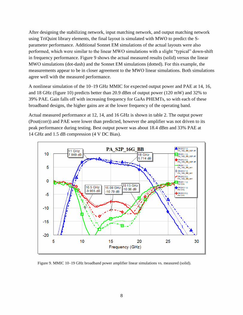
After designing the stabilizing network, input matching network, and output matching network
using TriQuint library elements, the final layout is simulated with MWO to predict the S-
parameter performance. Additional Sonnet EM simulations of the actual layouts were also
performed, which were similar to the linear MWO simulations with a slight “typical” down-shift
in frequency performance. Figure 9 shows the actual measured results (solid) versus the linear
MWO simulations (dot-dash) and the Sonnet EM simulations (dotted). For this example, the
measurements appear to be in closer agreement to the MWO linear simulations. Both simulations
agree well with the measured performance.
A nonlinear simulation of the 10–19 GHz MMIC for expected output power and PAE at 14, 16,
and 18 GHz (figure 10) predicts better than 20.9 dBm of output power (120 mW) and 32% to
39% PAE. Gain falls off with increasing frequency for GaAs PHEMTs, so with each of these
broadband designs, the higher gains are at the lower frequency of the operating band.
Actual measured performance at 12, 14, and 16 GHz is shown in table 2. The output power
(Pout(corr)) and PAE were lower than predicted, however the amplifier was not driven to its
peak performance during testing. Best output power was about 18.4 dBm and 33% PAE at
14 GHz and 1.5 dB compression (4 V DC Bias).
Figure 9. MMIC 10–19 GHz broadband power amplifier linear simulations vs. measured (solid).

9
Figure 10. MMIC 10–19 GHz output power and PAE performance simulation (14, 16, and 18 GHz).
Table 2. Power performance for the 10–19 GHz broadband amplifier.
12 GHz Die#1 11-19 GHz Fall12 TQP13 4V ; 45 mA
Pin(SG) Pout(SA) Pin(corr) Pout(corr)Gain I1(4V) PDC(mw) Pout(mw) Drn Eff PAE
-5.0 -1.32 -7.40 1.08 8.48 45 180.0 1.28 0.7 0.6
0.0 3.67 -2.40 6.07 8.47 45 180.0 4.05 2.2 1.9
5.0 8.71 2.60 11.11 8.51 45 180.0 12.91 7.2 6.2
10.0 13.35 7.60 15.75 8.15 45 180.0 37.58 20.9 17.7
12.0 14.66 9.60 17.06 7.46 47 188.0 50.82 27.0 22.2
14.0 15.43 11.60 17.83 6.23 42 168.0 60.67 36.1 27.5
14 GHz Die#1 11-19 GHz Fall12 TQP13 4V ; 45 mA
Pin(SG) Pout(SA) Pin(corr) Pout(corr)Gain I1(4V) PDC(mw) Pout(mw) Drn Eff PAE
-5.0 -1.89 -7.75 0.86 8.61 45 180.0 1.22 0.7 0.6
0.0 3.09 -2.75 5.84 8.59 45 180.0 3.84 2.1 1.8
5.0 8.15 2.25 10.90 8.65 45 180.0 12.30 6.8 5.9
10.0 13.00 7.25 15.75 8.50 45 180.0 37.58 20.9 17.9
12.0 14.58 9.25 17.33 8.08 47 188.0 54.08 28.8 24.3
14.0 15.61 11.25 18.36 7.11 42 168.0 68.55 40.8 32.9
16 GHz Die#1 11-19 GHz Fall12 TQP13 4V ; 45 mA
Pin(SG) Pout(SA) Pin(corr) Pout(corr)Gain I1(4V) PDC(mw) Pout(mw) Drn Eff PAE
-5.0 -3.23 -7.90 -0.33 7.57 45 180.0 0.93 0.5 0.4
0.0 1.73 -2.90 4.63 7.53 45 180.0 2.90 1.6 1.3
5.0 6.77 2.10 9.67 7.57 45 180.0 9.27 5.1 4.2
10.0 11.76 7.10 14.66 7.56 45 180.0 29.24 16.2 13.4
12.0 13.56 9.10 16.46 7.36 47 188.0 44.26 23.5 19.2
14.0 14.92 11.10 17.82 6.72 42 168.0 60.53 36.0 28.4

10
5. Conclusion
These broadband medium power amplifier MMICs were designed using some of the techniques
taught by Dale Dawson in the JHU Power MMIC Course. Previously, 2–6 and 5–11 GHz
broadband amplifiers were documented in technical report, ARL-TR-6278 (December 2012).
These two additional designs documented here extend lower (1–5 GHz) and higher (10–19 GHz)
in frequency. These broadband filter and matching techniques could be applied to parallel
combinations of transistors to increase power, but these simple one-transistor, single-stage
designs represent a proof of the design approach using actual fabricated and measured MMICs. It
should be noted that these broadband techniques were also used to successfully design two high
power broadband MMIC amplifiers at 3–5 and 4–6 GHz using TriQuint’s 0.25-µm gallium
nitride (GaN) process (see ARL-TR-59872 and ARL-TR-60903). Other broadband amplifier
designs of increasing difficulty are currently being designed at ARL, extending to higher
frequencies, parallel combined output devices, and cascaded gain stages.
These simple one stage MMIC amplifiers illustrate a broadband design approach and the
limitations that start with the device parasitics, the quality of the nonlinear and linear models
available, and the quality of the MMIC fabrication process.
While these designs were part of a JHU course, the design techniques and Microwave MMICs
would be of interest to Army and Department of Defense communications systems, sensors, and
wireless systems.
2Penn, J. Broadband, Efficient, Linear C-Band Power Amplifiers designed in a 0.25-µm Gallium Nitride (GaN) Foundry
Process from TriQuint Semiconductor; ARL-TR-5987; U.S. Army Research Laboratory: Adelphi, MD, May 2012.
3Penn, J. Testing of Broadband, Efficient, Linear C-Band Power Amplifiers; ARL-TR-6090; U.S. Army Research Laboratory:
Adelphi, MD, August 2012.

11
List of Symbols, Abbreviations, and Acronyms
ARL U.S. Army Research Laboratory
AWR Applied Wave Research
GaAs gallium arsenide
GaN gallium nitride
HP high-pass
JHU Johns Hopkins University
LP low-pass
MMIC monolithic microwave integrated circuit
MWO Microwave Office
PAE power-added efficiency
PHEMT pseudomorphic high electron mobility transistor

NO. OF
COPIES ORGANIZATION
12
1 DEFENSE TECHNICAL
(PDF) INFORMATION CTR
DTIC OCA
2 DIRECTOR
(PDFS) US ARMY RESEARCH LAB
RDRL CIO LL
IMAL HRA MAIL & RECORDS MGMT
1 GOVT PRINTG OFC
(PDFS) A MALHOTRA
4 DIRECTOR
(PDFS) US ARMY RESEARCH LAB
4 RDRL SER
(HCS) PAUL AMIRTHARAJ (PDF)
RDRL SER E
ROMEO DEL ROSARIO (1 HC)
JAMES WILSON (PDF)
JOHN PENN (3 HCS)
ROBERT PROIE (PDF)
ED VIVEIROS (PDF)