monolithic frequency integrated
TRANSCRIPT

MONOLITHIC INDUCTORS
FOR SILICON RADIO FREQUENCY INTEGRATED CIRCUITS
Mina Danesh
A thesis submitted in conformity with the requirements for the degree of Master of Applied Science
Graduate Departmeni of Electrical and Computer Engineering University of Toronto
Q Copyright by Mina Danesh 1999

National Library 1*1 .,,nada Bibliothèque nationale du Canada
Acquisitions and Acquisitions et BibEographic SeMces sentices bibliographiques
395 Wellington Street 395, rue Wellington Onawa ON K i A ON4 OüawaON K1AOW Canada Canada
The author has granted a non- exclusive licence allowing the National Library of Canada to reproduce, loan, distribute or sel1 copies of this thesis in microform, paper or electronic formats.
The author retains ownership of the copyright in this thesis. Neither the thesis nor substantial extracts 6om it may be printed or otherwise reproduced without the author's permission.
L'auteur a accordé une licence non exclusive permettant à la Bibliothèque nationale du Canada de reproduire, prêter, distribuer ou vendre des copies de cette thèse sous la forme de microfiche/film, de reproduction sur papier ou sur format élecîronique.
L'auteur conserve la propriété du droit d'auteur qui protège cette thèse. Ni la thèse ni des extraits substantiels de celle-ci ne doivent être imprimés ou autrement reproduits sans son autorisation.

Monolithic Inductors for Silicon Radio Frequency Integrated Circuits
Mina Danesh
Mas ter of Applied Science Department of Electncal and Computer Engineering
University of Toronto 1999
ABSTRACT
A novel parameter extraction technique is applied to the modeling of rectangular spiral
inductors and validated with measurements and simulations. To enhance the inductor quality
(Q) factor, a differentially excited symmetric inductor is used. Compared with a single-ended
configuration, the differential structure offers a higher Q-factor over a wider range of
frequencies. Application of the symmetric inductor mode1 is demonstrated using two
oscillator designs in which a differentidly excited symmetric inductor is compared with
conventionai spiral inductors. The symmetric inductor improves the overall circuit
performance and saves chip area.

ACKNOWLEDGMENTS
1 wish to thank Professor John R. Long for introducing me to the world of RF
electronics, and in particular, to microstrip structures on semiconductors, where
electromagnetics is coupled to electronics. He helped me in many ways throughout the course
of my studies. I appreciate his patience and his sympathy.
1 am also gratehil to my fellow graduate students and fiends: Ramesh Abhari (Yes,
you will be a professor!), Xidong Wu (for his Eastern philosophy and insightful comments),
Leesa and Kararn Noujeim. Micah Stickel, Sebastian Magierowski, Dickson Cheung, Ali
Sheikholeslarni, Vincent Gaudet, and Mr. Gerald Dubois who plays a special role in the group.
I also appreciate having met many interesting people, as well as the Massey College
comrnunity, who made my stay in Toronto much more enjoyable. 1 shall not forget Behzad, a
soulful musician.
.Je tiens à remercier mes parents et toute ma famille pour leur appui au cours de ces
deux dernières années. Karima a aussi tenu une place que je ne saurai décrire. Nilda et
Alexandra demeureront mes amies pour toujours.
1 am thankful for the NSERC Graduate Scholanhip which gave me the opportunity to
corne to the University of Toronto.
Finally, 1 wish to thank Prof. Christopher W. Trueman who knows how to guide his
students in their research.
"One is capable, if one is knowledgeable Knowledge (danesh) rejuvenates the soul"
Ferdowsi (940 - 1020 A.D.)
iii

This thesis is mainly aimed at RF circuit engineers. For those who do not have any
previous knowledge of how a spiral inductor works, the mechanisms behind microstrip
structures on a silicon substrate are presented. Chapter 2 explains the fundamentals of a single
microstrip line. Even though the world of electromagnetics may seem to exist in a realm other
than rnicioelectronics, this is in fact not the case. One must realize that electromagnetics (EM)
is the bais of everything electrical. 1 have tried to explain the interactions of the EM fields in
semiconductors as simply as possible. 1 deliberately did not give any formulations regarding
EM fields for they rnight confuse the reader. Since circuit engineers love circuits, equivalent
circuit models for monolthic inductors are given, which should simplify their application in a
circuit simulator.
For those who already have some experience with spiral inductors, Chapters 3 and 4
present new approaches to the modeling and optimization techniques for inductors.
Differential circuits may seem very familiar, but the designer rarely considers the EM
mechanism behind a differentially excited microstrip line or a different inductor configuration.
Chapter 4 gives an example of a cross-coupled oscillator where two inductor configurations
are compared.
A bibliography is given for those interested in further investigation. It is not an
extensive list, but it covers the major references.
Mina Danesh
September 1998
TABLE OF CONTENTS
. . LIST OF FIGURES ....................................................................................... v 11
LIST OF TABLES ................................................................................................................... x
.............................................................................. LIST OF SYMBOLS ........................... .. xi
........................................................... 1 . l Silicon Radio Frequency Integrated Circuits 1 ............................................................................ 1.2 Microwave Monolithic Inductors 3
.................................................................. 1.3 Purpose and Organization of this Thesis 5
2 . SILICON MICROSTRIP STRUCTURE CHARACTERISTICS .................................. 7 ........................................................................................ 2.1 Wave Propagation Modes 7 ...................................................................................... 2.2 Lumped Circuit Modeling 14
2.2.1 Single Microstrip Line Modeling ..................................... ... ................ 14 2.2.2 Spiral Inductot Modeling ........................ ...... .............................. 1 5
..................................................................................... 2.3 Inductor Quality Factor 17 ................................................. 2.4 Parameter Extraction Methods 1 9
2.4.1 Parameter Extraction €rom Two-Port Results ...................................... 19 ......................................................... 2.4.2 Analytical Parameter Extraction 2 I
................................................................................ a) Inductance 2 1 .................................................................................. b) Capacitance 22
c) Resistance ..................................................................................... *.23 .................................... d) Temperature Dependence .... ........................ 26 ............................................................. 2.5 Microstrip Line Simulation and Modeling 27
2.5.1 Approximation Mode1 ............................ .. ......................................... 27 2.5.2 Results .................................................................................................... 28
........... .................................... . 3 SPIRAL INDUCTOR MODELING ...... -34
............................................................................................................. 3.1 Motivation 34 ........................................................................................... 3.2 Modeling Procedure 36 ............................................................................................. 3.2.1 Induc tance 36
...................................................... 3.2.2 Series Resisrance .......................... .., -36 ............................................... ........................... 3.2.3 Substrate Parasitics ..., 37
a) Substrate Capacitance ............................................*...... ............ 37 .................................. b) Substrate Resistance ................................. .. 38
3.2.4 Line-to-line Capacitance ........................................................................ 38 3.2.5 Final Inductor Mode1 ............................................................................. .40
3.3 Test S tnictures ................. ... ........ .. ......... 4 1 3.4 Results and Discussion ..................... ... .... ,., .................................................. 41

.............................. 4 . SYMMETRIC INDUCTORS FOR DIFE'ERENTIAL CIRCUITS 46
.................................................... 4.1 Motivation ........................................................ 46 ....... .... .................. 4.2 Review of Q Enhancement Techniques ... .... ................. .47
...................................... 4.2.1 Optimization by Inductor Design .............. ............................ 4.2.2 Optirnization by Reducing Ohmic Losses .. 48
........................................ 4.2.3 Optimization by Reducing Substrate Losses 49 .............................................................. 4.3 Review of Inductor Chip Area Reduction 51
4.4 Proposed Method ................................................................................................... 52 ........................................................... 4.4.1 Inductors for Differentid Circuits 53
.............................................. . 4.4.2. Asymmetrical vs S ymmetncal Inductors 54 ........................................................... 4.5 One-Port Excitation Theoreticai Anaiysis 54
.................................... 4.6 Test Structure ................................................... 56 ............................................................................. 4.7 Syrnmetric Inductor Modeling 57
4.8 Measurement Procedure ....................................................................................... -59 4.8.1 Cdibration .............................................................................................. 59
.................. .....................*.........*............. 4.8.2 De-embedding Procedure .... -60 . 4.8.3 Single-ended vs Differential Parameters ......................................... 6 1
4.9 Results .................................................................................................................. -62 4.9.1 Parasitics ................................................................................................. 63
...................... .........*.............................*...*....... 4.9.2 Results and Discussion .. 63 ..................................................................................... 4.9.3 Sources of Error 68
.................................................... 4.9.4 Optimized Equivalent Circuit Models 68 ....................................... 4.9.5 Cornparisons with the Literature
4.10 Application ....................................................................................................... 70 .................................................................................. 4.10.1 Oscillator Design 70 ................................................................................. 4.10.2 Colpitts Osciilator 71
a) Operating Points .............................................................................. 72 b) Results ............................................................................................. 73
........................................ .................... 4.10.3 Cross-coupled Oscillator .... 73 ............................................................................ a) Operating Points 74
b) Results ............................................................................................. 75
............................................................... 5 . CONCLUSIONS ................................................. 78
REFERENCES ................................. f.. .. f. ............................................. 1

LIST OF FIGURES
................................................................ 1 . RF frontend: heterodyne iransceiver architecture 2
2 . Silicon resistivity as a function of doping concentrations of n-type (phosphorus) and p-type .................................................................................................................................. (boron) 2
3 . Microstrip line on silicon with a typical range of parameter values .......................... .... ......... 3
4 . Monolithic inductor configurations: (a) Microstrip line. (b) Meander line. (c) Single loop. (d) Circular spiral. (e) Octogonal spiral. (f) Rectangular spiral ............................ ............... 4
5 . Magnetic field lines for (a) an air coil. (b) a planar solenoid. and (c) a planar rectangular . . ..................................................................................................................... spiral inductor 5
6 . Electric field distribution of (a) quasiTEM. (b) slow.wave. and (c) skin-effect ................................................................................................................................... modes 7
7 . Resistivity-frequency mode chart for various oxidelsilicon thicknesses .............................. 8
....................................................................................... 8 . RlTD space for a 100 pm strip line 9
9 . Unnormalized vertical electric field for psi = 0.1 &cm ......................................................... 9
10 . Unnonnalized vertical electric field for psi = 10 R-cm ...................................................... I O
................................................. 11 . Unnormalized vertical electric field for psi = 10 k k m 1 0
12 . Unnormalized power in air. oxide and silicon for a single line. and even-mode and odd- mode excitations of two coupled microstrip lines (w = 10 pm. s = 5 pm) at 1 GHz .......... 11
13 . Resistivity-frequency mode chart for for a 10 pm wide microstrip line .............. 12
14 . (a) Re[qen] for different line widths . (b) Re[qen] for a 10 pm single line and coupled lines with 5 pm spacing . (c) Attenuation for single and coupled lines . (d) Real part and (e) imaginary part of the characteristic impedance for single and coupled lines .................. 13
. . .......................................................... 15 . Microstnp line equivalent circuit ................ .... .. 1 5
16 . Surface current flow for spiral inductors of (a) 3.75 tums and (b) 6.5 tums at 1 GHz ....... 15
17 . Electromagnetic field lines and line parameters for two coupled lines for odd- and even- . . mode excrtations ..........................~..................................................................................... 16
. . 18 . Simplified spiral inductor layout ...................................................................................... 17
19 . Compact lumped element inductor mode1 ..................... ... ..................*..........o...........m 17
2û . Equivalent L -port mode1 ..................... ......... ................................................................ 18
vii

21 . Measured real and imaginary parts of input impedance of a symmetric spiral indutor (N=5. w=8 pm. -2.8 pn) ............................................................................................................ 19
22 . Parameter fit circuit mode1 for measured and (simulated) CMOS spiral inductor .............. 20
.............................................................. 23 . Parameter extraction by the transmission matrix 20
24. MMIC microstrip line with shown electric fields ............................................................ ... 22
25.Oddmode capcitances for two coupled microstrip lines ............................................. ..... 23
..................................... 26 . Current distribution for an MMIC microstrip line ............ ...... -24
27 . Distributed mode1 of a microstrip line with two sections ................................................... 28
28 . Inductance L and series resistance r for 1 mm long microstrip lines .................................. 30
29 . Equivalent shunt substrate parasitics .................................................................................. 30
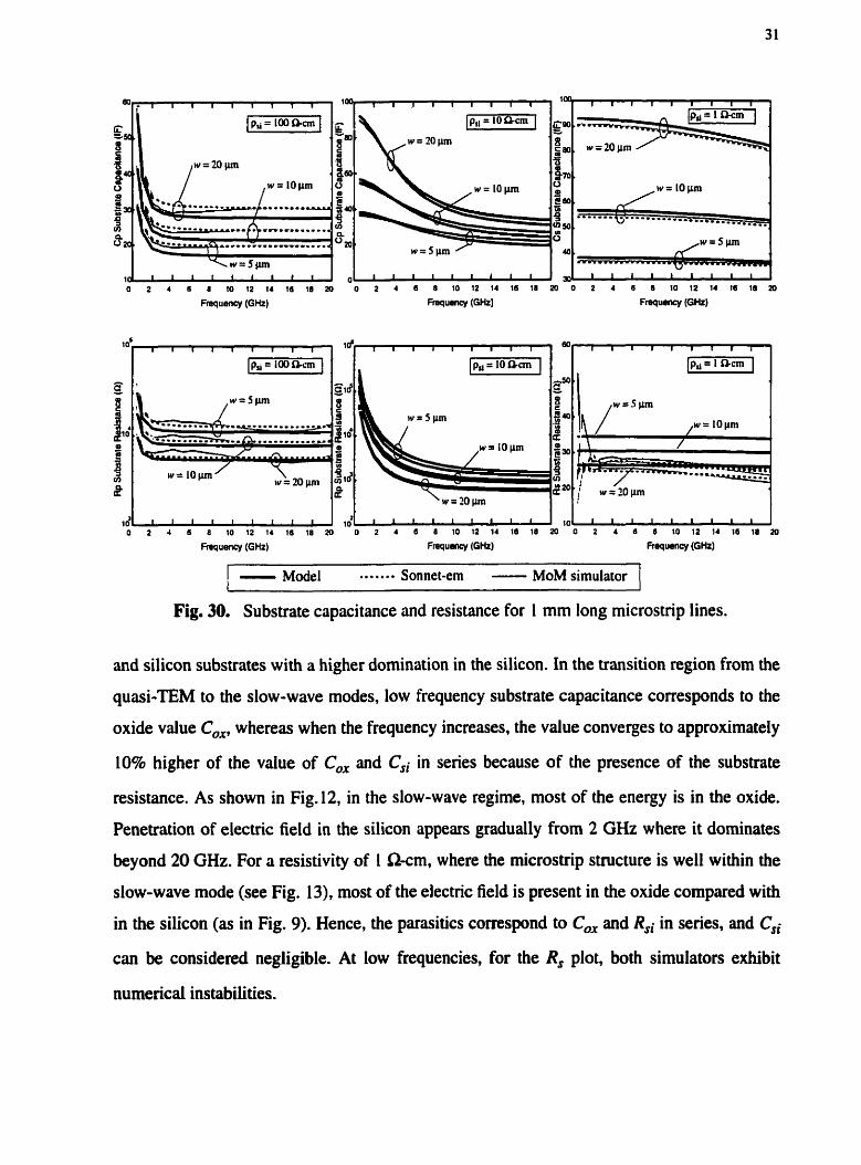
30 . Substrate capacitance and resistance for 1 mm long microstrip lines ............................. -31
31 . Quality factor for 1 mm long microstrip lines .................................................................... 32
32 . Lumped element circuit mode1 for one and a half tums of a spiral inductor .................. .*..35
33 . A 4.25 tum spiral inductor with different groups of coupled lines for line capacitances ... 37
34 . A 3.5 turn spiral inductor divided into two Iengths ....................................................... ..38
35 . Representation of the interwinding and underpass capacitances ........................................ 39
36 . Distributed mode1 for the spiral inductor equivalent circuit ............ .. ........................... *.40
37 . Photomicrograph of a 4.25 tum. 5 nH spiral inductor of 15 pm width and 1 pm spacing.41
38 . Transmission line equivalent parameters for the BiCMOS 4.5 turn inductor ..................... 42
39 . Transmission line equivdent parameters for the CMOS 4.25 turn inductor ....................... 43
40 . Q-factor cornparisons between models. measurements. and simulations for two spiral ........................................................................................................... .... inductors ......,. .. 45
. . 41 . Metal stacking in the oxide layer .................. .. ........ ..... ..... 4 8
42 . Electric and magnetic field distributions for rnicrostrip lines (a) without a ground shield. (b) with a ground shield. and (c) with a pattemed ground shield ................. ............ 49
....................................................................... .... 43 . Pattemed ground shield ........... ..... .. 3 0
44 . Removal of substrate parasitics by (a) selective etching of the underlying silicon. (b) fabrication of a dielectric membrane. or (c) etching part of oxide and silicon layers ......... 50
. . ................................................................................................ 45 . Multilevel spiral inductor 51
46 . Differential LNA.. ...........................~.................................................................................. 53

47 . Differential excitation for (a) two adjacent asymmebrical spiral inductors and a (b) Single . . ............................................. s ymmetncal inductor ... .......................... ............................ 53
. 48 Current paths for (a) singleended and (b) differential connections ................................... 55 . . 49 . Single-ended excitation mode1 .............................. ........ .................................................... S5
............................................................ 50 . Differential excitation mode1 .................... ...-.. .55
51 . (a) Inductor test structure layout . (b) Partial cross-sectional view of the inductor .............................. ................................................................................................ 56
. ..........*..................................*...**.. . 52 Open and short dummies for the inductor in Fig 5 1 (a) 57
53.3 tum symmetric inductor modeling with (a) group sectioning and (b) line-to-line ....................................................................................................................... capacitances 58
................ 54 . Parameter fit circuit mode1 for measured and (simulated) symmetric inductor ..59
..................................................................................................................... 55 . Dual probes S9
...................................................................... 56 . Device under test with associated pansitics 60
.................................................... 57 . Fiowchart of de-embedding steps ................................. .. 61
................................................................ 58 . Tko-port S-matrix with both configurations 6 1
59 . ïko-port 2-matrix with both configurations .................................................................... 62
......................................... 60. Open dummy structure parasitic histograms over 15 samples 63
61 . Inductor structure histograrns over 19 samples for (a) L and r at 500 MHz and (b) Q ....... 64
........................ 62 . Transmission line equivalent parameters for the 8 nH symmetnc inductor 65
63 . Measured and simulated resistive and inductive parts of input impedances for single-ended ................................................................................. and differentid connections ......... .. 66
64. Measured and simulated Q-factors for singletnded and differential excitations .............. 67
........................... 65 . Optimized equivalent circuit mode1 for both configurations ...... ... A 8
............. 66 . (a) LC tank and (b) equivalent resonator in a one-port oscillator .. .................. 71 . .
67 . Colpitts oscillator circuit . ............................... ................................................................... 71
. .................. 68 . Output oscillating voltage and phase noise for the Colpitts shown in Fig 67 -73 . . .... ................... 69 . Cross-coupled oscillator circuit ... .... ...
70 . Difkrential output voltage oscillation and phase noise for the 8 nH symmetric inductor ........ and two 4 nH asymmetric spiral inductors ..................... ...

LIST OF TABLES
Page
. .................................................... 1 Microstrip line inductance cornparison for psi = 10 a-cm 29
................... ...................................... . 2 Lumped element values for spiral inductor models .. 42
. ...........................................*......... 3 Typical inductor Q-factors for standard Si IC processes 46
4 . Cornparisons with senes and parallel connected inductors ............................................... -52
............................................................................................ . 5 Substrate and metal parameters 57
. ............................ 6 Lumped element values for the 5 tum symmetric inductor .... .................. 59
7 . Peak Q-factor cornparisons for single-ended and differential excitations ............................. 66
. 8 L and r values for Fig . 65 .................................................................................................... 69
9 . Substrate parasitic parameter fit for single-ended and differential excitations ...................... 69
................. 10 . Cornparisons of published references with the differential symrnetric inductor 70
. ......... 11 Element and source values for the Colpitts oscillator .... ..................................... 72
............................................................ . 12 Component values for the cross-coupled oscillator 74
13 . Comparisons between 8 nH symmetric and 4 nH conventional inductors ........................... 75
14 . Comparison of cross-coupled oscillator performance for both inductors ............................ 76

P s i
overall capacitance due to the overlap and interwinding capacitances
oxide capacitance from the strip line to the Si02/Si interface
silicon capacitance €rom the strip line to the ground plane without the oxide layer
skin depth
relative permittivity
effective relative pemittivity/dielectnc constant
frequency of operation
frequency at which the Q peaks
self-resonant frequency
inner gap between opposing groups of coupled strips of a spiral inductor
total length of a microstrip line structure
guided wavelength
transmission line inductance
number of tums of a spiral inductor
outer turn dimension of a rectangular spiral inductor
inductor quality factor
maximum inductor quality inductor value
resistance due to a strip conductor
dissipation due to the conductive silicon
metal sheet resistivity
silicon resistivity
spacing between two rnicrostrip lines
upper metal thickness
oxide thickness between upper and lower rnetais used for an underpass
oxide layer thickness
silicon layer thickness
rnicrostrip tine width
rnicrostrip line width for an underpass

Chapter 1
INTRODUCTION
1.1 Silicon Radio Frequency Integrated Circuits
With the emergence of wireless communications systems such as personal
communication services (PCS), wireless local area networks (WLANs), satellite
communications, and the global positioning system (GPS), interest has focussed on radio
frequency integrated circuits (RF ICs). In the 1980s, military applications drove the
development of monolithic microwave integrated circuits (MMICs) forward by fabbricating
passive and active circuit elements on the same semi-insulating gallium arsenide (GaAs)
substrate [l]. Compared with discrete and hybrid designs [2], the monolithic approach offers
low cost, improved reliability and reproducibility, smail size and weight, broadband
performance, and circuit design flexibility. Disadvantages of the monolithic approach, such as
process difficulties, low yields and poor performance, have largely been overcome [3], The
consumer electronics market favours silicon (Si) technology for its lower cost, higher yield,
and the potential for rnixing analog and digital circuits. Silicon bipolar and BiCMOS
technologies now offer performance comparable with GaAs in the low GHz frequency range
r 11-
Figure 1 shows the RF front-end architecture for a heterodyne transceiver, where
filters, amplifiers, mixers, and oscillators are needed for implementation. Inductors can be
used in al1 stages of an RF IC for the inputloutput matching circuitry and passive filters. They
are also convenient loads for active circuits, such as amplifiers and mixers, where lower noise
performance and 1-3 V supply voltages may be realized. However, implementing the inductor
onthip has been regarded as an impracticd task because of excessive substrate capacitance
and substantial resistive losses due to metallization and the conductive silicon substrate, which
degrade the overall performance of the circuit. Hence, d l inductive components were
integrated off-chip untii. in 1990, planar inductors were demonstrated to be feasible in modem
silicon technologies [4].

Down-Converter Down-Converter Mixer YFiiter Mixer Baseband
Antenna . Signal Out #+
BPF RX
IIF Synthesizer 1
Baseband Signal In
PA Up-Conve*er Amplifier IF Filter Up-Converter Mixer Mixer
Fig. 1. RF front-end: heterody ne transceiver architecture.
Compared with GaAs, on-chip inductors on silicon substrates have poorer
performance simply because of the low substrate resistivity. Depending on the dopant
concentration of the silicon wafer, the silicon resistivity c m be as low as 0.01 k m for
CMOS and 1 k m for bipolar, as illustrated in Fig. 2. For current bipolar and BiCMOS
technologies, the typical silicon resistivity ranges from 1 to 10 Q-cm, and for CMOS, from
0.01 to 1 Gcm. 0
N: Dopant concentration (cm?
Fig. 2. Silicon resistivity as a hinction of doping concentrations of n-type (phosphorus) and p-type (boron) [5].

1.2 Microwave Monolithic Inductors
Passive inductors are implemented with high characteristic impedance microstrip
lines fabricated on an insulating (Sioz) layer that lies on top of a silicon substrate and lower
ground plane, as shown in Fig. 3. The typical range of values for each parameter is indicated.
The silicon resistivity psi rnust be accounted for in transmission line losses, whereas the oxide
conductiviiy is on the order of 10-13 Slm, and hence is considered negligible. Because of finite
psi and narrow strip width, design guidelines for MMIC structures are not found in the
Iiterature, contrary to established design guidelines for MICs [6, 7, 8, 91 for which the fields
are in the quasi-TEM (transverse electromagnetic) mode [IO]. This will be considered in
Chapter 2.
Ground la ne
Fig. 3. Microstrip line on silicon with a typical range of parameter values.
Figure 4 shows some planar inductor designs. The single microstrip line, meander, and
single loop inductors provide inductances up to 0.5 nH and are seldom used. The meander
inductor is designed to conserve chip area, but a better approach is to wind the microstrip line
in a spiral, as shown in Fig. 4 (d), (e), and (f). Mutual coupling resulting from the closely
spaced lines adds to the self-inductance of the transmission line, increasing the overail
inductance. However, because of practicd restrictions in the mask making process, the
circular shape is implemented as an octogonal or a hexagonal spiral. vpicaiiy, inductances up
to 20 nH are realized on-chip with spiral configurations. The rectangular spiral is the most

Fig. 4. Monolithic inductor configurations: (a) Microstrip line, (b) Meander line, (c) Single loop, (d) Circular spiral, (e) Octogonal spiral, (0 Rectangular spiral.
commonly used design due to its layout simplicity, however, higher losses are obtained
compared with a circular layout, Le., for equal inductances, as high as a 10% increase in the
metallization loss results [ I I l . Its parameters include the outer dimension OD, the strip width
w, the spacing between lines s, the number of turns N, and the gap between opposing groups
of coupled lines G. The inner turn is connected to the outer circuitry by an underpass, routed
via a lower level metal, or an air-bridge.
A coil or solenoid is the most farniliar inductive component; thus the design of a planar
spiral inductor may seem odd at first. Figure 5 illustrates the magnetic field lines for a coi!, a
planar solenoid, and the rectangular spiral. Closely spaced windings of the coil provide flux
iinkages on the top and bottom windings, and the flux lines pass through the middle of the
coil. The sarne idea applies to the planar solenoid, but this design is not suitable for monolithic
integration [12]. For the rectangular spiral, groups of coupled lines are located on the same
plane, and the flux lines pass through the substrate layers, which results in greater inductance
values compared with the planar solenoid.

' Top metal I-, / \
wer level metal
Fig. S. Magnetic field lines for (a) an air coil, (b) a planar solenoid, and (c) a planar rectangular spiral inductor.
1.3 Purpose and Organization of tbis Thesis
The purpose of this thesis is to study the behavior of rnicrostrip line structures on
silicon in order to mode1 monolithic inductors as equivalent electricd circtuits and to design
higher quality inductors for enhancing the performance of RF circuits. Chapter 2 provides an
in-depth analysis of propagation issues for Si MMIC technology. This introduces the RF
engineer to the design considerations for microstrip elements on a silicon substrate.
IUustrations of various line parameters as a function of silicon resistivity and frequency will
be presented to support theoretical predictions. A lumped element mode1 is proposed for the
single rnicrostrip line, which is compared with numerical simulation results from commercial
electromagnetic simulators.
Chapter 3 focusses on the rnodeling of spiral inductors in silicon technologies. A new
inductor model and lumped element parameter extraction technique, based on the single
microstrip line case, is compared with experimentai and simulated results.
Present monolithic inductors can achieve a maximum Q-factor of 10, posing a
limitation for narrowband circuits. Viuious Q enhancement and chip area reduction techniques
have been proposed in the literature, as described in Chapter 4. A closer look at differential
symmetric circuits that integrate spiral inductors leads to a differentially excited inductor
instead of a singleended layout where one end of the port is grounded. The differential
configuration provides a higher Q (up to a 50% increase in the peak Q) by lowering the
substrate parasitics which degrade the inductor performance without altering the fabrication
process. A symmetric inductor structure is proposed that is suitable for differential circuits. A
model for the symmevic inductor is also presented. Measured and simulated inductor Q-
factors agree to within 10%. To demonstrate the advantages and improvement in performance
associated with a differentiai excitation of a symmetric inductor versus single-ended
conventional asymmetric spiral inductors, the performance of single-ended and differentiai
Colpitts oscillators at 2 GHz are compared.

Chapter 2
SILICON MICROSTRIP STRUCTURE CHARACTERISTICS
The first section of this chapter introduces the electromagnetic theory behind a
microstrip line on a silicon substrate for which different propagation modes are defined.
Lumped pi-type equivalent circuits for single and coupled microstrip lines are reviewed. The
last section of this chapter will show how the propagation modes can be related to a lumped
element equivalent circuit.
2.1 Wave Propagation Modes
Studies of propagation on a microstrip
line on a SiO2/Si substrate were first analyzed
using a parallel-plate waveguide mode1 [ 10,
131. By observing the associated loss for
various values of silicon resistivities and
frequency ranges, three specific regimes were
identified, each associated with a different
propagation mode, as illustrated in Fig. 6 for
the electric field distribution.
In Fig. 7, these three regimes are
shown in a resistivity-frequency mode chart
for typical oxide and silicon thicknesses. The
regimes are defined as follows:
1) When the product of frequency and
silicon resistivity is high, the silicon substrate
/-
(a)
+- Line C- SiOz
e Si
' Line
c- Si02
e Si
Ground plane
Fig. 6. Electrtic field distribution of (a) quasi-TEM, @) slow-wave, and
(c) s kin-effect modes [ LOI.
acts as a dielectric with a srnall dielectric loss tangent; the fundamental mode is close to the
TEM mode and is therefore called a quasi-TEM mode. Its frequency range is defined for
1 C

2) When the product of frequency and silicon resistivity is moderate, a surface wave
propagates dong the transmission line at the Si02/Si interface with a propagation velocity
smaller than in the previous case. This is the slow-wave mode for which
3) When the product of frequency and silicon conductivity is large enough so that the
silicon substrate acts as a lossy conductor or an imperfect ground plane, the fundamental
mode is called the skin-effect mode (where the skin depth 6 = ,,/-) (m) is on the
order of the silicon thickness, i. e., 6 = 160 pm at 1 GHz for psi = 0.01 R-cm). This mode
appears for
f 2 0.4 fa (Hz). (3)
Standard Si bipolar processes range in the slow-wave, transition region of the slow-
wave to quasi-TEM, and quasi-TEM modes in the 1 to 10 GHz frequency range. CMOS RF
applications are well within the slow-wave and even in the skin-effect regimes.
Silicon resistivity @cm)
Fige 7. Resistivity-frequenc y mode c hart for various oxide/silicon thic knesses.
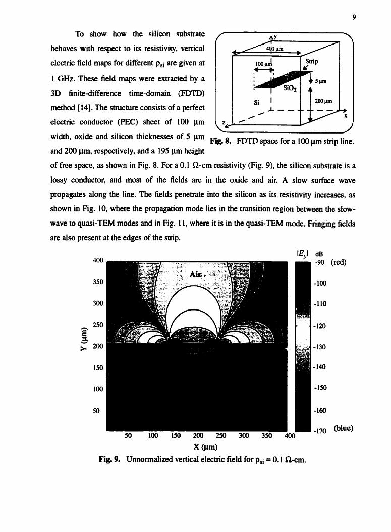
To show how the silicon substrate
behaves with respect to its resistivity, vertical
electric field maps for different psi are given at
1 GHz. These field maps were extracted by a
3D finite-difference the-domain (FDTD)
method [14]. The structure consists of a perfect
electric conductor (PEC) sheet of 100 prn
width, oxide and silicon thicknesses of 5 pm Fig, 8. FDTD space for a 100 stnp line. and 200 Pm, respectively, and a 195 pm height
of free space, as shown in Fig. 8. For a O. 1 R-cm resistivity (Fig. 9), the silicon substrate is a
lossy conductor, and most of the fields are in the oxide and air. A slow surface wave
propagates dong the line. The fields penetraie into the silicon as its resistivity increases, as
shown in Fig. 10, where the propagation mode lies in the transition region between the slow-
wave to quasi-TEM modes and in Fig. 1 1, where it is in the quasi-TEM mode. Fringing fields
are also present at the edges of the strip.
50 100 150 200 250 300 350 4
X (w) Fig. 9. Unnormalized vertical electric field for psi = 0.1 R-cm.

(blue)
(blue)
Fig. 11. Unnormalized vertical electric field for p i = 10 kn-cm.

A two-dimensional numerical simulation using the spectral domain approach (SDA)
[15, 16, 171 was used to extract the power in different layers, as shown in Fig. 12, for a single
line and two coupled microstrip lines of 10 pm width and 5 pm spacing. (The SDA is a less
computer intensive numerical method appropriate for 2D planar strip lines in a shielded box.
Convergence was achieved with a box length of 10 mm with 4000 points and an air height
greater than 1 mm.) Al1 subsequent figures will show results for a 5 pm thick oxide and a
350 pn silicon layer. In the skin-effect mode, most of the fields penetrate the oxide layer and
only slightly penetrate the silicon because of its high loss tangent (> 100 at 1 GHz). For the
slow-wave regime, most of the active power is still in the oxide, but the rest is dissipated in the
silicon by a conduction current. A large amount of reactive power is exchanged between
substrate layers because of the movement of charges at the Si02/Si interface [IO]. Due to this
energy transfer, a slower propagation velocity results. In the quasi-TEM regime, for a single
microstrip line and evenly excited coupied lines, most of the energy is transmitted in the
silicon substrate (as compared with the oxide) [IO]. More electric field lines pass through the
,,,,,,,, Power in oxide
Silicon resistivity (&cm)
Fig. 12. Unnormalized power in air, oxide and silicon for a single line, and even-mode and odd-mode excitations of two coupled microstrip lines (w = 10 Pm, s = 5 pm) at 1 GHz.

conductive layer in the even-mode than in the single line case, whereas in the odd-mode, a
substantial portion of the electric field is concentrated between the two strips [18, 191.
Figure 13 illustrates the slow-wave and quasi-TEM regimes for the range of silicon
resistivities and frequencies of interest for RF ICs, given the effective dielectric constant E ~ R
value of a 10 Fm wide single microstrip line. As previously defined, a slow-wave propagates
for certain silicon resistivity and frequency ranges, which results in higher effective dielectric
constants. The quasi-TEM effective dielectric constant is around 5 (region shown in blue),
while its value increases to reach a constant (1 1.6) in the slow-wave regime.
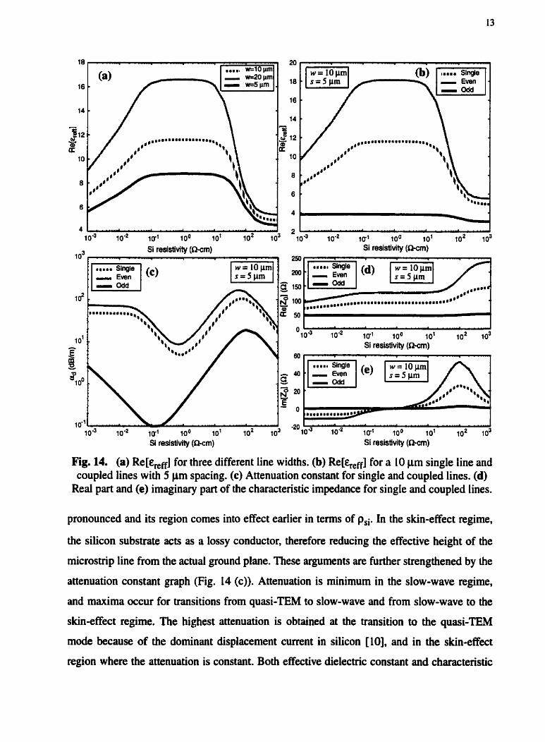
Figure 14 shows the transmission line parameters for single and coupled microstrip
lines at a frequency of 1 GHz using the SDA rnethod. Decreasing the line width causes less of
the field to be contained in the lossy silicon substrate than in the oxide and the air, which
reduces the value of the effective dielectric constant in the slow-wave region. This is also
observed for an odd-rnode excitation. Hence, as the width increases, the skin-effect is more
Silicon resis tivity (hm)
Fig. 13. Resistivity-fiequency mode chart for for a 10 pm wide microstrip line.
, -3 Si resistivity ( m m )
0 l L o ~ 10.~ 10-1 100 toi yYr' 102 - d 103
Si resistivity (mm)
Si resistivity (Scm) Si resistivity (Gcm)
Fig. 14. (a) Re[hff] for three different line widths. (b) Re[qefr] for a 10 lm single line and coupled lines with 5 pm spacing. (c) Attenuation constant for single and coupled lines. (d)
Real part and (e) irnaginary part of the characteristic impedance for single and coupled lines.
pronounced and its region cornes into effect earlier in terms of psi. In the skineffect regime,
the silicon substrate acts as a lossy conductor, therefore reducing the effective height of the
microstrip line from the actual ground plane. These arguments are further strengthened by ihe
attenuation constant graph (Fig. 14 (c)). Attenuation is minimum in the slow-wave regime,
and maxima occur for transitions from quasi-TEM to slow-wave and from slow-wave to the
skineffect regime. The highest attenuation is obtained at the transition to the quasi-TEM
mode because of the dominant displacement cunent in silicon [IO], and in the skin-effect
region where the attenuation is constant. Both effective dielectric constant and characteristic

impedance are constant in the slow-wave regime. The real part of the characteristic impedance
follows the curves of the power flow in air, as shown in Fig. 12, whereas the reactive
component is similar to the reactive power in the silicon layer.
For typical RF applications, it has been shown that due to the silicon resistivity value
and frequency of operation, the slow-wave propagation mode and transitions between quasi-
TEM and skin-effect modes are excited. This demonstrates the importance of the process
chosen for the design of monolithic inductors. The influences of these propagation modes will
be described throughout this chapter.
2.2 Lumped Circuit Modeüng
For RF design, representation of microstrip lines by an equivalent circuit is needed in
circuit simulators. PhysicaVelectrical behaviours of monolithic inductors are translated into
lumped element equivalent circuit models. The microstrip line is the simplest physical layout
for a planar inductor for which an equivalent circuit is determined. This single microstrip line
circuit model can also be applied to spiral inductors which consist of groups of coupled strips.
2.2.1 Single Microstrip Line Modeling
The electrical behaviour of a transmission line can be approximated over a range of
frequencies by a lumped element equivalent circuit model. For a microstrip transmission line
fabricated in silicon technology, an appropriate equivalent circuit is shown in Fig. 15, where L
is the inductance of the line, and r is the series resistance mainly due to conductor losses. It is
a frequency dependent element which accounts for the edge, proximity, and skin effects [20]
on the current flow, and for the conductive silicon substrate [IO], due to the current fîow
paraIlel to the strip current that is induced in the substrate. Induced eddy currents are
attributed to the proximity effect [21]. The shunt parasitics result from a combination of
capacitances, involving the insulating layer of silicon dioxide (Cm), the underlying substrate
(CSi) and its dissipation (Rsi) [IO]. For an electrically short microstrip line where 1 c h$10, a
single rt-section equivalent circuit (Fig. 15) is sufficient, whereas for a longer line, a
distributed model should be used.

Fig. 15. Microstrip line equivalent circuit.
2.2.2 Spiral Inductor Modeling
A spiral inductor consists of groups of coupled microstrip lines. Modeling the spiral
requires knowledge of the currents fowing on the conductor. The current is a time varying
component and Rows continuously dong the spiral. Currents on the same group of coupled
strips flow in the same direction, which results in an even-mode excitation for the adjacent
strips, as shown in Fig. 16 (a). This holds when the total length of the spiral is less than a
quater of the guided wavelength (where the inductor is self-resonant) and there is a negligible
phase shift in the signal voltage or current. Currents on opposing groups of coupled strips flow
OD= 191 pn w = 1 O p n s= 1Spm N=6.5 tums Substrate parameters given in [23].
Fig. 16. Surface current fiow for spiral inductors of (a) 3.75 turns and (b) 6.5 tums at 1 GHz.

in different directions, as in Fig. 16 (a), and hence, the odd-mode is excited. Also, the effect of
the air-bridge or underpass cm disturb the current distribution on the upper metal layer of the
spiral, depending on the separation between the two metal layers [22]. As shown in Fig. 16 (b),
decreasing the inner gap of the spiral causes a non-uniform current distribution. This current
crowding effect is due to induced eddy currents on adjacent strips in the same group and in
inner tums, which degrades the total inductance and increases the series resistance [23,24].
Figure 17 illustrates the electromagnetic field lines and how they influence the
transmission line parameters for both odd and even-modes. In the latter case, both currents on
adjacent strips flow in the same direction, which results in a positive mutual inductive
coupling &, thereby increasing the total inductance. For silicon MMICs, K, typically ranges
from 0.5 to 0.8 [21]. Only the electric fields from the strips to the ground plane are present.
Therefore, tighter spacing increases the inductance and decreases the substrate capacitance
because of reduced electric fringing field lines. For an odd-mode excitation, currents flow in
the opposite direction, which results in electric field lines between the strips through the air,
oxide and silicon layers. Moreover, negative mutual inductive coupling K, degrades the total
inductance. Hence, for a spiral inductor, r substantial gap (G > 5w) must separate opposing
groups of coupled strips [24, 251. In conclusion, a spirai inductor can have excitations of
8 1
t t
Odd-modé excitation Even-mode excitation
Electric field lines @ Outward flowing cumnt K: Mutual inductive coupling coefficient <, , , Magnetic field lines @ Inward flowing current
Fig. 17. Electrornagnetic field lines and line parameters for two coupled lines for odd- and even-mode excitations.

mixed modes, making it difficult to understand and model.
The spirai inductor can be considered to be a
series of electrically short microstrip lines (Fig. 18)
connected by mutual inductive coupling coefficients,
interwinding (line-to-line) capacitances, and added
parasitics due to the bends (considered negligible:
Cbcd c 1 fF and Lbd < - 0.05 nH [26]) [25, 271.
Added capacitance due to the overlap between the
tums of the spiral and the center-tap underpass or
cross-over should also be taken into account. A more
I \ Group of coupled electncally
Po
rt 2
-- - -
Fig. 18. Simplified spiral inductor layout.
common representation of a spiral inductor is a compact model, shown in Fig. 19, which is
derived from a single microstrip line equivalent circuit. Here, L and r represent the total
inductance and resistance of the inductor, respectively. Shunt parasitics model the outer
winding at Port 1, and the inner winding at Port 2. Using a conventional spiral inductor results
in an asymmetry in the layout, which is represented by two sets of substrate parasitic values
[25]. Co represents the overall line-to-line capacitance resulting €rom the combination of
interwinding and overlap capacitances.
1 Port I @.ri Po*,
Fig. 19. Compact lumped element inductor model.
2.3 Inductor Quality-Factor
The performance of an inductor is measured by its quality-factor (Q). It is defined as
the ratio of the energy stored to the total dissipation per cycle for a sinusoidal excitation [28]:
energy stored Q = 2r- = 0 . energy stored energy lost per cycle average power loss '
From a circuit point of view, other interpretations of Q can be used, such as those from the
-3 dB bandwidth at the angular resonant frequency (a,) or the rate of change of the phase shift
at resonance, defined iis follows:
For the case of an inductor, only the energy stored in the magnetic field is considered,
whereas energy stored in the electric field, due to parasitic capacitances, counteracts the
inductive energy.
For a series L-r circuit connected as a one-port, the Q-factor is defined as
and for a parallel Lp-rp circuit,
vdid until the inductor's first self-resonance, where Zin is the input irnpedance and Y, is the
input admittance of the one-port structure. A resonance occurs when the peak magnetic
energy equals the peak electric energy or XL = - XC, where C is the total circuit capacitance,
and the resonant frequency is
fsr = I/(~xJL-c) (Hz).
In this case and beyond the self-nsonant frequency, no net magnetic energy is available.
Closed-fonn expressions approximating the
monolithic inductor Q-factor are given by Yue and Wong
[29] by considering the circuit in Fig. 20, where Cp and
Rp replace the substrate shunt parasitics Co,*, Csi1 and \ +
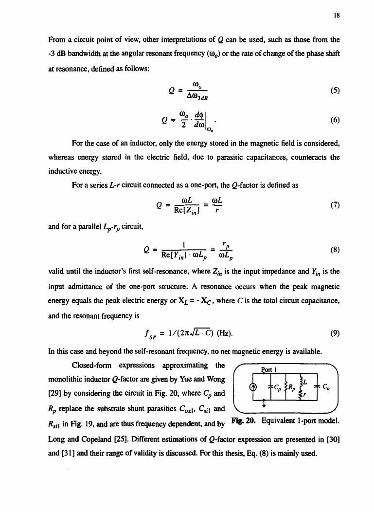
Rsil in Fig. 19, and are thus frequency dependent, and by Fig. 20. Equivalent 1 -port model.
Long and Copland [25]. Different estimations of Q-factor expression are presented in [30]
and [3 11 and their range of validity is discussed. For this thesis, Eq. (8) is mainly used.

2.4 Parameter Extraction Methods
This section describes how inductor parameter values for the lumped elements are
obtained. The first method does not require knowledge of the physical layout of the structure.
From the two-port S-parameters, given either by measurement or simulation, series and shunt
impedances for the compact mode1 of Fig. 19 are derived. The second method consists of
determining analytically the L, R, and C cornponent values from the physical layout and
fabrication process specifications.
2.4.1 Parameter Extraction from 'ho-Port Results
A microstrip inductor is a two-port element. The S-parameters are determined from
simulation or measurement. Series inductance L and resistance r in the compact modei (see
Fig. 19), are first derived at low frequencies from the one-port input impedance of the two-
port network, as
Figure 2 1 gives an example of the red and imaginary parts of the input impedance for
a spiral inductor derived from measured two-port S-parameters [32]. At low frequencies
(Kd >> lXLl), r is given by Re[Zi,J, and L as Im[Zin]/2rcf; they are 7.7 and 7.5 nH,
respectively. As the frequency increases, inductive reactance increases and capacitive and
resistive parasitics corne into play, causing a resonance near 6.3 GHz, when the resistive part
of the input impedance is maximum and the reactance is zero. Beyond resonance, the
O 5 10 15 20 O 5 10 15 20 Frequency (GHz) Frequency (GHz)
Fig. 21. Measured real and imaginary parts of the input impedance of a spiral indutor (N=5, w=8 Pm, s=2.8 km).

reactance is negative, and hence the inductor behaves as a capacitor.
Using an optimizer to fit the measured and simulated S-panmeters, approximate
values for shunt parasitics and overall capacitance Co are obtained, as shown in Fig. 22. Data
for a CMOS 4.25 turn spiral inductor are fit to a frequency range of 0.5 to 6 GHz (below the
self-cesonance). The shunt parasitic capacitances are lower ai the output port (Port 2) because
the inner turn of the spiral is shorter in length than the input port (Port 1) outer turn. This
results in an asymmeûy in the parameter values for Co,, Csi, and Ri in the model.
(5) " (7.1) Port 1 L = S n H r=7.1Q Port 2
O I O
Fig. 22. Parameter fit circuit rnodel for meiisured and (simulated) CMOS spiral inductor.
The previous method involved fitting the parameter values to a set of two-port results
over a range of frequencies, using a cornputer. Another way is to translate the two-port S-
parameters to P set of lumped element values at each frequency point. The S-parameters are
converted into the propagation constant y and the characteristic impedance 2, of a
transmission line, from which the lumped elements (L, r; C,,, Rp and Co) are derived [33].
Figure 23 summarizes the procedure in a flowchart. Simulators such as Sonnet-em provide
qe% and 2' values for both ports which can be applied to the method of Fig. 23 by directly
extracting the component values per unit length.
cos h y1 2, sinh yL
coshyL 1 : $ : = yrz,
I \
Port 1 : L r : Port : - 0
Fig. 23. Parameter extraction by the transmission matrix .

2.4.2 Analyticai Parameter Extraction
This section provides a review and a discussion of the extraction methods used for
each lumped element parameter, as well as new concepts.
a) Inductance
Inductance is defined as the ratio of the total flux linkages to the current to which they
link [34]. Mutual inductance caused by the magnetic interaction between two currents adds to
the self-inductance. Depending on the configuration of the conductors, the inductance may be
expressed as a function of the physical dimensions, as for an N-tum coi1 or solenoid [35].
Greenhouse derived the total inductance of a planar rectangular spiral inductor [36], based on
the closed-form inductance formulas for the self and munial inductances of rectangular
conductors published by Grover [37], resulting in an inaccuracy of less than 5% compared
with measurements. However, these inductances were derived assuming a thick substrate
(W « substrate height) and a static value which does not take into account the electncal length
of the spiral inductor at high frequencies where the inductor resonates. Krafesik and Dawson
[38] approached these effects by including a negative m u ~ d inductance when the spiral outer
diameter is comparable to the ground plane distance, ;uid taking into account propagation
delay around the spiral. The experimental results agreed to within 5%.
Other authors have provided crude estimates of the total spiral inductance with closed-
fom expressions [39, 401. Mohan et al. [41] obtained an inductance expression for square
spirals with tight line spacings (s < w/2), which does not take into account the metal thickness.
It has been shown that the inductance matrix can be obtained from the free space capacitance
matrix [Cd with respect to the ground plane, defined as = [ cai, ] [42]. This
definition can be useful if a full-wave or 2D method gives the capacitive parameter values in
matrix form. Full-wave methods can also be applied to obtain more accurate results [3 11.
However, Greenhouse's method c m be easily implemented in a cornputer program and
cm be modified for any rectangular layout geometry. Therefore, this method will be used
throughout this thesis.

b) Capacibnce
The capacitance C relates the ratio of the total charge to the potential difference
between two conductors. For two parallel conducting plates, C is expressed as a hnction of
the physical dimensions and substrate layer permittivity as
where d is the separation between the two plates, assuming a uniform current distribution on
the plates and d c< w and 1 [43]. For an MMIC microstrip line where w is on the order of 2 to
50 Pm, which is comparable to the oxide thickness, and is much smaller than the silicon
thickness (200 - 500 pm), these assumptions are no longer valid.
As illustrated in Fig. 24, electric field lines are
non-uniform; hence, fiinging fields must be taken into
account. The total capacitance consists of Cpp, the
parallel plate capacitance, and of Cf for the fringing
capacitance. To provide accurate capacitance values,
several approaches have been used. For computational
efficiency, a iwo-dimensional numericai analysis
technique is often used under static assumptions. For
Fig. 24. MMIC microstrip line with electric fields shown.
coupled strips, odd and even-mode capacitances have been calculated [44, 451, and for
multiconductor strips, capacitance matrices are obtained [46,47,48,49,42]. Basis hinctions
for the non-uniform current, which mode1 the surface edge effect on the charge density for a
microstrip line, are used to enhance the accuracy of soiutions [SOI. Other methods, such as the
boundary element method (BEM) [51], the finite-difference (FD) [52], or the measured
equation of invariance (ME0 [53], have been used. (The references do not provide an
exhaustive list of publications.)
The overlap capacitmce for the underpass Cu may be approximated using (1 1)
where th is the separating distance between the upper and lower metals used for the
underpass in the oxide layer, and wu is the line width of the underpass. Because of additional

stray fields surrounding the overlap, it has been shown that Cu is increased by a factor of 1.5 to
1.7 relative to (12) [54].
The interwinding capacitance is the f
line-to-line coupling capacitance between
adjacent conducting strips. Due to differences
in phase between the voltage on each strip. the
interwinding capacitance is the odd-mode
coupling capacitance in the substrate and air.
Figure 25 illustrates the electric field lines and
associated odd-mode capacitances for two Fig. 25. Odd-mode capacitances for two
coupled microstrip Iines. The coupling coupled microstrip lines.
capacitances, Cgd and Cg=, can be calculated
from the corresponding coupled stripline geometry filled with substrate dielectric and air,
respectively [ S I . This method is efficient for two coupled microstrip lines only. Mutual
coupling capacitances can be also obtained using a full-wave analysis technique for any
arbitrary number of conductors [3 1,461.
The overall capacitance Co in shunt with the series inductance and resistance is a
combination of interwinding and the underpass or bridge capacitances. This will be discussed
in Chapter 3.
c) Resistance
From Ohm's Iaw, the resistance of a conductor is defined to be the ratio of the
electrornotive force to the strength of the current that it produces. The DC resistance depends
on the nature of the conductive material and the temperature [56].
Sen'es Resistance due to MetaUiaziîon
Resistance is defined by the current distribution on the rnictrostrip line, and in the case
of silicon, also by the conduction current inside the silicon substrate. Resistance due to the
strip line varies with frequency in a complicated manner. They are four factors to take into
account: 1) DC, 2) Edge effect, 3) Proxirnity effect, and 4) Skin-effect [20].
At low frequencies, approaching DC, the current is unifomily distributed over the
conductor. The DC resistance Rd, of a microstrip line is determined from the sheet resistivity
p, of the metal. vpical values for aluminum and aluminum alloys are on the order of
30 mR-pm.
As the frequency increases (low MHz range), the current distribution changes due to
the induced electric field in the conductor (produced by excess charges). The current
concentrates at the sharp edges of the conductor. A reduction of the effective conductor cross-
section increases the resistance [20]. Proxirnity effect also takes place when a nearby
conductor carrying a time-varying current induces a rnagnetic field on the conductor which
causes a current to Row in the opposite direction [2 1,571.
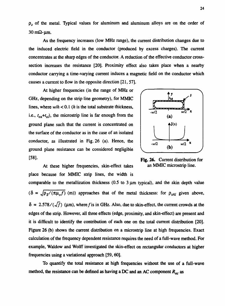
At higher frequencies (in the range of MHz or
GHz, depending on the strip line geornetry), for MMIC
lines, where wlh < 0.1 (h is the total substrate thickness,
Le., t,,+tSi), the microstnp line is far enough from the
ground plane such that the current is concentrated on
the surface of the conductor as in the case of an isolated
conductor, as illustrated in Fig. 26 (a). Hence, the
ground plane resistance cm be considered negligible
i581-
At these higher frequencies, skin-effect takes
place because for MMIC stnp lines, the width is
Fig. 26. Current distribution for an MMIC microstrip line.
comparable to the metallization thickness (0.5 to 3 pm typical), and the skin depth value
(6 = ,,/-) ((m)) approaches that of the metal thickness: for p s ~ ~ given above,
6 = 2.578/(Jf) (pm), where f is in GHz. Also, due to skin-effect. the current crowds at the
edges of the strip. However, al1 three efiects (edge, proximity, and skin-effect) are present and
it is difficult to identify the contribution of each one on the total current distribution [20].
Figure 26 (b) shows the current distribution on a microstrip line at high frequencies. Exact
calculation of the frequency dependent resistance requires the need of a full-wave method. For
example, Waldow and Wolff investigated the skin-effect on rectangular conducton at higher
frequencies using a variational approach [59,60].
?b quanti@ the total resistance at high frequencies without the use of a full-wave
method, the resistance can be defined as having a DC and an AC component R, as

R =
Several closed-form resistance
P, 1 Rdc + Roc = - tM - W
+ Ra, (a-
approximations are found in the literature. Pettenpaul et al.
1391 give an expression based on measured data for wide strips (w > 50 pm), Eo and
Eisenstadt [6 11 denve an expression assuming an exponentially decaying current hinction,
and Sonnet-em uses a square root frequency dependence to account for the skin-effect [62].
For this thesis, the series resistance expression chosen for the strip Iine rsl is based on
[6 11, given as
-tM/6 which accounts for the metallization skin depth 6. The 6 ( I - e ) terrn is equivalent to an
effective metal thickness t,f [63]. However, Eq. ( 14) assumes that the skin-effect occurs from
frequencies just above DC, which is not the case for narrow strip widths. To account for the
skin-effect influence at a higher frequency, a transition frequencyf, is defined when 6 = tM,
which is also dependent on the t~ 1 w ratio. Hence, the resistance is normalized at a frequency
f, and the values below this frequency threshold is approximated by the DC resistance, as the
following:
where r, is the resistance atf, defined by (14). Another approximation is also proposed by
Eo and Eisenstadt [6 11, for modeling the side wall current of microstnp lines.
The resistance rs accounts for losses due to the longitudinal component of the
conduction current in silicon. It is a function of the square of frequency [IO] and dominates
the inductor loss mainiy as a function of psi and$ It is approximated as
6 f L o t : i r6=3.5x 10 *-• Psi
1 (QI

where f is in GHz. rg was obtained by fitting Eq. (16) to the series resistance curves given by
simulators. Hence, the total resistance becomes
The accuracy of Eq. (17) will be illustrated through examples.
As the silicon resistivity decreases (psi cc 0.1 Q-cm), the silicon acts as a lossy ground
plane and its effect becomes dominant. For very low resistivities (< 0.1 m s c m ) , the silicon
can be considered as a lossy rnetal. Hence. the total resistance must take into account the
resistance due to the silicon 'ground plane' because the strip is only on top of the oxide layer,
such that the current distribution on the strip is mainly concentrated on the lower side close to
the silicon 'ground plane'. The surface current on the ground plane is also concentrated under
the strip so that the resistance of the ground place converges to rd at high frequencies and for
Substrate Resistance due to Conductive Silicon
Similarly, computing the substrate resistance R, is not an easy task. Full-wave
methods that account for substrate resistivity are required. However, if the silicon capacitance
is known, the following result is obtained h m the resistance and capacitance definitions [64,
651 :
s i + Psi RSi = - (m. ' s i
d) Temperature Dependence
Ar1 important aspect in designing RF circuits is the ability of the circuit to function
within a broad temperature range (typically, -50 to 8S°C). Metailization and substrate
resistivities depend on temperature according to the following linear approximation:
P - P o = p , a v - TOI ( 19)
where T, is a selected temperature, p, is the resistivity at that temperature, and a is the
temperature coefficient [66]. From experimental results, it has k e n shown that for AYCu
(98% AL), a is around 0.34%PC, whereas for a 15 R-cm silicon resistivity, it is 0.35%PC
[67]. As the substrate doping decreases, and hence a higher resistivity p, ensues, a higher
temperature dependence is obtained, as seen from Eq. (19) [5]. An increase in the temperature
results in an increase in the metal series resistance causing Q to decrease. The substrate
resistance would, on the contrary, dorninate the determination of Q at frequencies beyond the
Q peak, and cause an increase in the Q. Nevertheless. for applications of inductors in silicon,
the metallization resistance has the dominant effect on Q 1671. The inductance is not affected
by temperature variation, and the substrate capacitance has a temperature coefficient of - 0.18WC [67], which can be considered negligible for MMIC microstrip structures because a
10% change in the substrate capacitance would cause less thm a 5% decrease in the overall
performance such as Q. Hence, for MMIC spiral inductors on a SiOz/Si substrate. it is the
effect of temperature on the series resistance which should be considered.
2.5 Microstrip Line Simulation and Modeling
To verify what has been described throughout this chapter, various 1 mm long
microstrip Iines were simulated by two Full-wave commercial electromagnetic simulators,
Sonnet Software em and HP-EESof Series IV Momenturn, referred to as the MoM (method of
moment) simulator in this thesis, and an approximate rnodel was also developed. Each
simulator uses the method of moments in the spatial domain. Momentum uses a mixed
potential integral equation [68], whereas Sonnet is based on an FFT [69]. Both use a rooftop
expansion or basis funciions for the current distribution. Results for line widths of 5, 10, and
20 pm and for silicon resistivities of 1, 10, and 100 Q-cm will be presented and discussed. The
oxide and silicon thicknesses are 5 pm and 350 Fm. respectively. The duminum metal
thickness is 2 pm with a 30 mR-pm resistivity.
2.5.1 Approximation Mode1
The spectral domain technique was used to derive the substrate capacitances. For each
substrate layer, the program was run for the particular substrate thicknesses: first, for that of
the oxide from which C,, was detennined; and second, for that of the lossless silicon layer,
where Csi and L were obtained. For ratios of tsi/tox > 50, the electric field distribution in the
silicon layer does not change significantly whether a thin layer of oxide is present or not. For
typical thicknesses (i.e., t,, = 5 pm and tsi = 300 p), this assurnption holds. For this model,
the Iine inductance value was approximated to be the same as the value for the silicon layer

aione because L depends on physical dimensions, and the difference is negligible ( ~ 1 % ) when
compared with the structure's exact simulation. The program does not account for metal
thickness. Other closed-form expressions could also be used, such as that of Greenhouse. The
total series resistance r accounts for the skin-effect and the conductive silicon, defined in
Eq. ( 17). Here, R, was detennined from Csi as in ( 18).
In the worst case, where w = 20 pm at 20 GHz, an effective relative permittivity of
13.6 was obtained. Hence the guided wavelength is 4.06 mm. For a lumped element
equivalent circuit to hold for the microstrip line of 1 mm, a distributed model with at least
three sections must be used, assuming that each section is smaller than one-tenth of the guided
wavelength. For clarity, Fig. 27 shows a two-section distributed model. The series impedance
and the shunt admittance are divided by the number of sections. To obtain the resulting Q,
Port 2 is shorted, and the input impedance is determined as a function of ZA and ZB.
Fig. 27. Distributed model of a microstrip line with two sections.
2.5.2 Results
Table L compares the line induc tance values obtained from the electromagnetic
simulators and approximate expressions for p, = 10 k m . Only Greenhouse [36] and
Pettenpaul [39] account for the metai thickness. Sonnet-em and Momentum give the highest
values, differing by as much as 10% from the other methods.
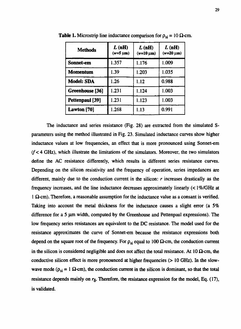
Table 1. Microstrip line inductance cornparison for psi = 10 S c m .
1 Lawton [70] 1 1.268 1 1.13 1 0.991 1
The inductance and series resistance (Fig. 28) are extracted from the simulated S-
parameters wing the method illustrated in Fig. 23. Simulated inductance curves show higher
inductance values at low frequencies, an effect that is more pronounced using Sonnet-em
(f< 4 GHz), which illustrate the limitations of the simulators. Moreover, the two simulators
define the AC resistance differently, which results in different series resistance curves.
Depending on the silicon resistivity and the frequency of operation, series impedances are
different, mainly due to the conduction current in the silicon: r increases drastically as the
frequency increases, and the line inductance decreases approximately linearly (c 1 %/GHz at
1 k m ) . Therefore, a reasonable assumption for the inductance value as a consant is verified.
Taking into account the metd thiçkness for the inductance causes a slight error (a 5%
difference for a 5 pm width. computed by the Greenhouse and Pettenpaul expressions). The
low frequency series resistances are equivalent to the DC resistance. The model used for the
resistance approximates the curve of Sonnet-em because the resistance expressions both
depend on the square root of the frequency. For psi equal to 100 $2-cm, the conduction current
in the silicon is considered negligible and does not affect the total resistance. At 10 k m , the
conductive silicon effect is more pronounced at higher frequencies (1 10 GHz). In the slow-
wave mode (psi = 1 Q-cm), the conduction current in the silicon is dominant, so that the total
resistance depends mainly on rs. Therefore, the resistance expression for the model, Eq. (17),
is validated.

1 - Mode1 ....-.. Sonnet-em - MoM simulator 1
Fig. 28. Inductance L and series resistance r for 1 mm long microstrip lines.
As shown in Fig. 29, for substrate parasitics, two
models were used, where Cp and Rp are the paralle1 equivalent,
and C, and Rs are the series equivalent frequency dependent
lumped elements corresponding to the actual shunt impedance.
In Fig. 30, substrate parasitic plots are shown for each
of the three silicon resistivity values. The approximate mode1
provides reasonable values, within 5% of the simulated results.
Therefore, representing the substrate parasitics as a series
Fig. 29. Equivalent shunt substrate parasitics.
connection of the oxide and silicon parasitics seperately as assurned, is verified. The
frequency behaviour of the equivalent total substrate capacitance depends on the distribution
of electric fields in the oxide and the silicon layers. For p i equal to 100 k m , substrate
parasitics are constant beyond 3 GHz, proving that the quasi-TEM mode is excited (see
Fig. 13). Since Rp is in the kn range (> 5 kR), Cp is equivalent to the series combioation of
Cm and C+ for frequencies beyond 3 GHz where the electnc field is distributed in the oxide
- Mode1 Sonnet-em - MoM simulacor ( --
Fig. 30. Substrate capacitance and resistance for 1 mm long microstrip lines.
and silicon substrates with a higher domination in the silicon. In the transition region from the
quasi-TEM to the slow-wave modes, low frequency substrate capacitance corresponds to the
oxide value Cox, whereas when the frequency increases, the value converges to approximately
10% higher of the value of Cox and C, in series because of the presence of the substrate
resistance. As shown in Fig.12, in the slow-wave regime, most of the energy is in the oxide.
Penetration of electric field in the silicon appears gradually from 2 GHz where it dominates
beyond 20 GHz. For a resistivity of 1 Q-cm, where the microstrip structure is well within the
slow-wave mode (see Fig. 13), most of the electric field is present in the oxide compared with
in the silicon (as in Fig. 9). Hence, the parasitics correspond to Cm and R, in series, and CSi
can be considered negligible. At low frequencies, for the Rs plot, both simulators exhibit
numerical instabilities.

For overall performance visualization of the microstrip line, Q-factor plots are shown
in Fig. 31. The microstrip line model presented compares well with the full-wave simulated
data. Agreement within 10% is achieved. Curves obtained from the MoM simulator have a
higher peak Q at a lower frequency than those from Sonnet-em and the model, mainly because
of the difference in the series resistance. For a psi of 100 atm, the MoM simulator Q curves
do not follow the curve obtained from the mode1 because of numericd instabilities of the
simulator for the substrate parasitics (see Fig. 30). The Q of the model is higher than the
simulators', since the Q follows oL/r until8 GHz, thus the influence of the series resistance r
is more pronounced on the overall Q. As shown in Fig. 28, r of the model is smallet than that
of the simulators' for frequencies beyond 7 GHz.
1 - Malel .---+.- Sonnet-em - MoM simulator 1 Fig. 31. Quality factor for 1 mm long microstrip lines.

As the silicon resistivity decreases, so does the Q and the self-resonant frequency due
to higher substrate capcitance (Cm > Csi) and lower substrate resistance (Rsi). With an
increase in the linewidth, higher Q and lower self-resonance are obtained because of lower
series resistance and higher substrate parasitics, even though the line inductance decreases,
although not as significantly.
The mode1 proposed for a microstrip line can be applied to coupled Iines or a spiral
inductor by including the negative and positive mutual inductances and capacitances, as will
be shown in the following chapter.

Chapter 3
SPIRAL INDUCTOR MODELING -- -- -
This chapter describes a simplified rnodel and parameter extraction technique for
spiral inductors in silicon technology. The model is vaiidated using experimental
measurements and full-wave electromagnetic simulations.
3.1 Motivation
Spiral inductors are utilized in many RF/MMIC applications. For computer-aided
design (CAD) purposes, a lumped element equivalent circuit, or electrical model. is required.
An accurate CAD model is needed to predict correctly the overall performance of an RF
circuit. Full-wave commercial electromagnetic simulators are computationally intensive, i. e.,
they require a great deal of CPU time and memory. Therefore. microstrip inductor models,
derived from layout and process fabrication parameters, are needed. Several modeling
techniques are reviewed in the following paragraphs.
As shown in Fig. 22. the parameters of a single ir-type equivalent circuit can be found
by cornputer optimization so that the measured S-parameters for a spiral inductor and the S-
parameters of the equivalent circuit model agree to within a specified tolerance. The compact
rnodel is the simplest representation of the spiral; it was used by Ashby et al. [7 11 and Yue et
al. [63]. The totai inductance and series resistance are computed from closed-form
expressions, as given in Sections 2.4.2 a) and c). However, the total capacitive and resistive
substrate parasitics are fit to the measurements using an optirnizer [71] or to the measured
properties of the silicon substrate [63].
A more accurate equivalent circuit for the entire rectangular spiral inductor is obtained
by dividing the spiral into groups of multiple coupled lines. Some approaches derive the
inductance and resistances of each line segment in a group in closed-form, whereas the
parasitic capacitances are obtained from two-dimensionai static numetical computations, as
described in Section 2.4.2 b) [38,72. 251. Figure 32 gives such a lumped elernent equivalent
circuit model For a one-and-a-half mm rectanplar spiral inductor. The mode1 consits of a

Fig. 32. Lumped element circuit model for one and a half tums of a spiral inductor.
series connection of electrically short microstrip line segments joined by inductive coupling
coefficients (K, for the same group of coupled strips, and K, for opposite groups) and mutual
line-to-line capacitive cornponents Cm. Each segment is represented by its equivalent circuit
model (Fig. 15). Capacitances Cbend due to the microstrip bends crin dso be taken into
account [25]. Full-wave methods have also been used for extracting the individual lumped
elements of each line segment [27] or sets of coupled lines [3 1,731, which are then connected
together to fom the entire spiral. The lurnped equivalent circuit cm become highly complex;
however, it can still be easily handled by a circuit simuiator tool, such as SPICE. This
equivalent circuit can also be reduced to a compact model [25].
Building upon the simplicity of the compact model, a circuit with only the minimum
number of lumped elements, a novel extraction method is proposed for the parasitics and the
series resistance of the entire spiral structure; it does not require computer optirnization. This
technique simplifies the representation of the spiral inductor, and it can be easily integrated
into a circuit simulator. It uses closed-form expressions for the total inductance, resistance,
and underpass capacitance. A 2D static numericd method extracts the line capacitances,
reducing computation time with minimal loss of accuracy. The interwinding capacitances are

obtained from the odd-mode mutual coupling of two coupled lines. The longitudinal
component of the conduction current in a semiconducting substrate is included in the
resistance model to account for al1 significant sources of loss. This method is numerically
more efficient than full-wave modeling techniques and is sufficiently accurate for design
purposes. Measured and simulated results are compared with the proposed model to establish
its range of validity.
A mode1 was developed in Chapter 2 for a single microstrip line. A new approach is
presented, bûsed on the parameter extraction procedure for a single rnicrostrip line. Instead of
regarding the spiral inductor as a succession of microstrip lines coupled together by groups, as
shown in Fig. 32. this approach is derived from looking at the entire structure. The new
procedure is outlined below for each extracted parameter.
3.2.1 Inductance
The total static inductance of a spiral inductor is calculated using Greenhouse's
method, where the self, mutual positive and negative inductances are computed and summed
to obtain the total inductance of the spiral structure [36]. The width and spacing of the lines,
the number of tums, the thickness of the metal, and the outer dimensions of the spiral must be
specified. For the range of silicon resistivities of interest (psi 2 I km), the inductance can be
regarded as a constant, as shown in Fig. 28 for a single rnicrostrip line.
3.2.2 Series Resistance
The ohrnic loss represented by the series resistance of the inductor is a frequency
dependent parameter. The expression given by Eq. (17) is used for the model, which takes the
skin-effect and the effect of the conductive silicon into account. An in-depth discussion is
given in Section 2.4.2 c).

3.2.3 Substrate Parasitics
a) Substrate Capacitance
The substrate capacitances have series components due to the oxide and silicon layers.
In the case of a single microstrip line. these capacitances were calculated by extracting the
values for the oxide layer only, Le., the ground plane at the Si02/Si interface, and then
repeating this calculation for the silicon layer (oxide removed and o,i + O). Hence, two line
capacitances were obtained separately. This method is also applied to the spiral inductor
mode1 . The line-to-ground capacitance is
obtained from the even-mode capacitance
of adjacent coupled strips. The
capacitance extraction method is
explained more clearly by giving an
example for a 4.25 tum square spiral
inductor, as shown in Fig. 33. The spiral is
divided into sections of one, two, three,
four, and five coupled strips. The total
capacitance is a summation of group
capacitances times the lengths of the
groups. For a 4.25 tum spiral, the
capacitance is approximated as
c4 c2 \
group of 4 group of 2
group of I
group of 3 c3
group of 5 c5
- -- - --
Fig. 33. A 4.25 tum spiral inductor with different groups of coupled lines for line
capacitances.
where are the line capacitances for the different groups of coupled strips, computed
from a two-dimensional numerical method. For each layer of substrate ( S i 4 and Si), the
capacitances per unit length are given for each group of coupled strips, and the total
capacitances obtained from (20).

The parameter extraction method for the
total substrate capacitances gives the average
overall capacitance of the spiral inductor. To
approximate for the asymmetry in the spiral
inductor distributed by the two ports, the N tum
spiral is divided in two at NI2 tums. As shown in
Fig. 34, the length conespondhg to the first half of
the spiral Ig, is higher than that for the length of
the second half 1g2. The fractions l g l / l and 1g2/l Fig. 34. A 3.5 tum spiral inductor divided into two lengths.
give the ratio for the substrate capacitances.
Hence, Ck = 2Cmi Igk/l, where k= l ,2.
Representation of the compact model using two different sets of substrate parasitics at
each port does not significantly improve the overall accuracy when compared with the total
average values, using (20) only. Therefore, in this thesis, the same set of parasitic values are
used in the compact model, reducing the total computational time.
b) Substrate Resistance
The silicon resistance is obtahed using Eq. (18) from the total silicon capacitance.
Contrary to the model used for a single microstrip line, where Ri is derived from C, (the totai
silicon capacitance of the line), a factor of 2 in Eq. (21) is a fitting parameter that adjusts the
substrate parasitics to correspond to the measurements and full-wave simulations. Therefore,
the resulting silicon resistance becomes
3.2.4 Lhe-to-line Capacitance
The line-to-line capacitance Co is a combination of the interwinding and underpass
capacitances. The underpass connects the inside of the spiral to the extemal circuitry; its
capacitance is approximated by the parallel-plate capacitance between the top metal and the
Iower metal used for the underpass, as given by Eq. (12). Due to stray fields, additional
capacitance results. It has k e n shown that the total underpass capacitance is 1.55 to 1.7 times

higher than that of the parallel-plate model [Ml. The interwinding capacitance between
adjacent strips has to be taken into account in the model due to phase shift along the spiral.
resulting in a potential difference between each tum. This was not considered by other authors
[3 L, 741 who approximate the overall line-to-line capacitance as a surnmation of underpass
capacitances only.
The interwinding capacitance is the odd-mode coupling capacitance in the substrate
and air between two coupled strips [ S I , as described in Section 2.4.2. b). The thickness of the
metal conductors must dso be taken into account in the 2D numerical method. The coupling
capacitance Cc is a summation of Cgd and Cm, the gap capacitances in the dielectnc and the
air, respctively. Cd is defined as the average difference of the odd-mode and even-mode
stsipline-to-ground capacitances with the dieiectric filled with oxide. The gap capacitance in
the silicon is considered negligible. Similarly. Cg, is obtained with air as dielectric, and it
should not take the fringing capacitances into account since these were included in the
calculation of Cd. Hence, Cc is the average sum of Cgd and Cm.
As shown in Fig. 35, the different rnutual
coupling capacitances Cm are distributed along
the spiral. Each Cm is obtained from the
coupling capacitance Cc times the length of each
set of two coupled strips and is represented by
two cornponents at each end of the coupled
strips. The coupling between non-adjacent strips
of the same group has k e n considered
negligible. Underpass capacitances Cu are also
distributed along the segments where the
underpass crosses the spiral. These are
connected to Port 2.
The total Iine-to-line capacitance Co is
(Port 1
Fig. 35. Representation of the interwinding and underpass capacitances.
obtained €rom optimization. Each line segment is approximated as an inductance to represent
the series impedance of the microstrip Lne. The two-port network consisting of interwinding
capacitances bridged between iine segments is translated to a capacitance in shunt with an

inductance. The optirnization is performed by fining the equivalent two-port parameters of the
entire structure to a single capacitance, that is, Co, in shunt with an inductance L,, at
frequencies near the resonance of Co and L,.
3.2.5 Final Inductor Mode1
The inductor equivalent circuit is distributed into n = 4N identical sections, as
illustrated in Fig. 36. The maximum OD represented as a single Iumped element pi-section is
assumed to be less than one-tenth of the guided-wavelength, defined as 1
where c the speed of light and Lqis the self-resonant frequency of the spiral inductor defined
Justification for the number of sections chosen is as follows. Assuming a maximum
line width of 50 pm and an effective dielectric constant of 100, Eq. (22) predicts that &$ is
40 GHz for an OD of 300 Pm. The usefui range of frequencies for a spiral inductor with an
OD of 300 pm is typically below 4 GHz, or one order of magnitude lower in frequency.
Therefore, a conservative estirnate for the maximum number of sections n required is the total
number of segments 4N. The final equivalent circuit model is shown in Fig. 36.
Fig. 36. Distributed model for the spiral inductor equivalent circuit.

Ground
Port 1
Ground
Ground
Port 2
Ground
Fig. 37. Photomicrograph of a 4.25 tum, 5 nH spiral inductor of 15 pm width and 1 Pm spacing.
3.3 Test Structures
Two different spiral inductor structures are used to verify experimentally the model
described above. The first inductor consists of a 4.5 Nm spiral with OD = 241 Pm, w = 10 pm,
and s = 5 Pm, fabricated in a BiCMOS process, (see [25]). The specified psi can range
between 5 R-cm and 15 Bcm due to the uncertainty in the starting wafer. The underpass is
15 pm wide and is 1 pm from the upper metal.
A second 4.25 tum 5 nH square spiral inductor, fabricated in a medium resistivity
silicon (1 < psi < 10 Q-cm) CMOS process, is also used for validation. Figure 37 shows the
top view of a 15 pm width inductor with its signal and ground pads.
3.4 Resuits and Discussion
Table 2 gives the lumped element values obtained from the model for each inductor.
The total length of both inductors is around 3.2 mm. The maximum number of sections
required to account for the distributed model of the coi1 is 18 for the BiCMOS inductor. It has
been verified that n = 8 is a sufficient value. Parameters for the CMOS inductor confirm the

component values extracted from optimization fit of measured and simulated data (see
Fig. 22). In the model, Cm represents Cd in Fig. 22, and C, and R, are the averaged values
of Cril,l and Rsil,2, respectively. To account for the asymmetry of the spiral, Table 2 also
gives the corresponding substrate parasitics at each port. Using the averaged values in the
compact model does not alter the overdl performance such as Q-factor.
Table 2. Lumped element values for spiral inductor models.
* Values in ( ) are the calculated subtrate puasitics at Port1 and Port2, respectively.
To compare the different results, the equivalent transmission line parameters are
extracted using the method shown in Fig. 23. In the case of low silicon resistivities, the
representation of the substrate parasitics as a series capacitance and resistance is adequate, as
shown for a single microstrip line in Fig. 30.
7 i
a - -
O 1 2 3 4 5 Frequency (GHz)
- O 1 2 3 4 5
Frequency (GHz)
O 1 2 3 4 S Frequency (GHz)
1 -Mode1 - Measurement - MoM simulaior *-----* Sonnet-em 1 Fig. 38. Transmission line equivalent parameters for the BiCMOS 4.5 tum inductor.

Line parameters as a function of frequency are given in Figs. 38 and 39 for the two
different spiral inductors. The low frequency inductance agrees with the total inductance
obtained using Gnenhouse's method. The MoM simulator predicts an inductance that is
higher by 10%. The agreement between simulations for the series resistance is less good: low
frequency resistance ~ L F approximates the DC resistance, but the Sonnet-em resistance model
gives a 10% higher r p Moreover, neither simulator seems to properly predict the influence of
the skin-effect and substrate conductive losses. However, substiate elements extracted from
the simulation compare reasonably well with the measurements. In Fig. 38, measurement
errors for the substrate parasitics result from inaccuracies due to the network analyzer at low
frequencies (fc 1.6 GHz). The model provides a substrate resistance as much as 30% higher
than the measurements due to lower Csi compared with the input port C,, of a spiral inductor.
The difference in substrate resistance does not alter significantly the overall performance of
the inductor.
I O 2 4 6
Frequency (GHz)
1 - Mode1 - Measurement - MoM simuliitor
Fig. 39. Transmission line equivalent parameters for the CMOS 4.25 mm inductor.

The Q-factors (Fig. 40) for both inductors show the influence of the line parameters.
The model agrees well with the measurement curve. The Q-factors from the MoM and
Sonnet-em simulators differ from the model and measurement curves because of the
inaccurate series impedance values. The low frequency (f < 1 GHz) Q demonstrates the
variation in series resistance: Sonnet-em has a higher r ~ f i and the MoM simulator a lower rm
which explains the difference in the peak Q and the shift in the frequency at which Q peaks.
The inductor model compares well with the experimental results. so it can be used to
predict the actuai performance of an inductor More it is fabricated. Moreover, the mode1 can
be easily implemented in a circuit simulator, given prior knowledge of process parameters and
the physical layout of the inductor. The various lumped element parameter extraction methods
can be implemented in a single computer program. The input parameters are OD, w, w,, s, N,
top tsi9 tw t ~ ~ ~ , psi, and ps. Since the single element section can be represented as a
subcircuit, implementation in the circuit simulator such as SPICE is simplified. The
application of the inductor model will be demonstrated for an oscillator circuit, described in
Chapter 4. The modeling technique proposed in this thesis cm also be used for MMIC spiral
transfomiers. The s m e extraction procedure for the substrate parasitics would apply.
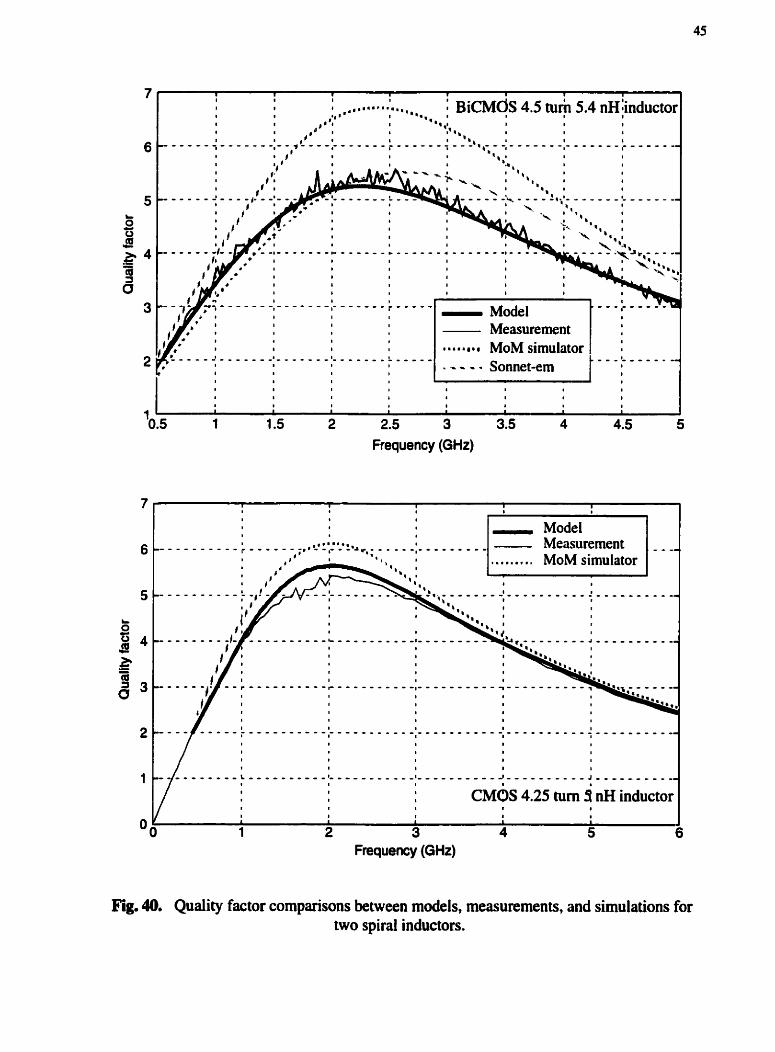
7 1 1 1 B I I 1 I 1 I
I
I
l
1 : B ~ C M ~ S 4.5 tum 5.4 nH:inductor
- Measurement i n * 8 8 8 a MoM simulûtor
'0.5 B 4 B I B 4 1
1 1.5 2 2.5 3 3.5 4 4.5 5
Frequency (GHz)
Frequency (GHz)
Fig. 40. Quality factor cornparisons between models, measurements, and simulations for two spiral inductors.

Chapter 4
SYMMETRIC INDUCTORS FOR DIFFERE:NTIAL CIRCUITS
This chapter proposes a new inductor design that is suitable for differential circuits, in
particular. First, current inductor configurations and their performance are reviewed. The
theoretical background for singleended and differential excitations of a microstrip structure is
presented. Measurernents, simulations, and an inductor mode1 are then compared. Finally,
oscillator circuits are designed to illustrate an application of inductors and their modeis.
4.1 Motivation
The quality factor of microstrip structures is limited by the series resistance of the
metallization and, in the case of silicon technology, losses in the conductive substrate. The Q-
factor is typically less than 10 for a metal-insulatoc-semiconductor (MIS) structure fabricated
in a production silicon IC technology. Table 3 Iists typical Qs for different inductor designs
and silicon resistivities. For most CMOS technologies, Q-factors range from 2 to 4.
Table 3. Spicai inductor Q-factors for standard Si IC processes.
B ipolar
BiCMOS
BiCMOS
BiCMOS
CMOS
CMOS
Dimensions Psi Reference L (nH) OD/w/s/&
(pm) l N
Long 1253 1.8 10 3/3C -/ 151 1.5/5/ 3.5
Yue [63] 8 10 2 / 3 0 3ûû/ 1 3 / 7 1 4.5 1 7
Craninckx[24] 3.2 0.0 1 -135 r=85 / 8.5 / 1 .S / 0.7 14
Lutz [27j 10 0.0 1 0.75 1 34 245,230 / 10 / 1.81319.5

For narrowband wireless applications, such as LC tanks in oscillators, Qs of at least 10
are required [l]. Thus, due to the lirnited Qs available on-chip, low noise and very narrowband
applications require external high Q resonaton. Front-end filters are comrnonly placed off-
chip. However, integrated spiral inductors are currently used for on-chip impedance matching
and tuned loads [74,75].
4.2 Review of Q Enhancement Techniques
The inductor Q-factor is constrained by the rnetallization resistance, the conductive
loss due to the silicon substrate, and the substrate parasitic capacitances (which limit the
inductor self-resonant frequency). Several approaches have been applied to enhance the Q at
its peak and/or the self-resonant frequency. Before applying the enhancement methods, a set
of inductor design guidelines must be followed.
4.2.1 Optidzation by Inductor Design
A set of design rules for rectangular spiral inductors [25, 761, most of which have
already been presented in Chapter 2, are summarized as follows:
1) The space between the outer spiral mm and any other surrounding metal structures
must be at least 5w to avoid coupling between structures.
2) Tight magnetic coupling, using the minimal allowable spacing s, not only
niaximizes Q but also reduces the total chip area.
3) A 10 to 15 Fm strip width w is close to optimum for the Q-factor when the
frequency of operation is in the 1-3 GHz range. Another consideration is the skin effect at
higher operating fiequencies for increasing line widths.
4) Opposing sets of coupled Lines must be separated by at least 5w to allow enough
magnetic flux to pass through the hollow part of the spiral, and also to minimize the
conductive substrate eddy cumnt effects.
5) The oxide layer should be as ihick as possible to reduce the substrate parasitic
capacitance, thus increasing the inductor self-resonant frequency.
6) The metal thickness and resistivity are fixed by the fabrication technology; however,
multilevel metal processes allow for the parailel connection of metals or metal stacking to
reduce the ohmic losses at the expense of decreasing the oxide thickness.

4.2.2 Optimization by Reducing Ohmic Losses
Investigation of varying sûip iine metd thickness has been conducted by Long and
Copeland [25], showing a 67% increase in the peak Q-factor for a 1.8 nH inductance resulting
from a 1 pn to 3 pm metal thickness increase. whereas Yue et al. [63] show a 37% increase
from a 1 pm to 2 pm increase for an 8 nH inductor. Hence, doubling the metal thickness does
not result in twice the Q-factor. For a double metal thickness, the DC resistance is halved.
However, the total resistance is higher thm expected due to the skin-effect. An effective
ihickness te,defined using ( 14) shows that a 1 pm and a 3 prn thick Al metallization have tu
equal to 0.84 pm and 1.83 pm at 1 GHz. respectively [63]. Moreover, an increase in the metal
thickness causes the inductance to decrease by a small percentage (~10%). Hence, for twice
the metal thickness, a doubling of the Q-factor is impossible.
With the metal layers provided by Via connections
modem process technologies, metd strips cm Upper metal
be stacked by using vias, as shown in Fig. 41. Lower rnetals
Lower metal layers are used for underpasses. Underpass
c For a 2 nH inductor, a 50% increase in the peak Fig, 41. Metal stacking in the oxide layer. Q-factor was obtained by shunting three metal
layers as in Fig. 41. The DC series resistance was nearly halved. The process used had a
greaier oxide thickness (10 pm instead of 4 pm) to allow a reasonable (> 2.1 pm) separation
distance between the lowest metal and the silicon substrate. The Q increased by 30% if a 5-
level metal process was used instead of 4 levels because the underlying oxide thickness was
doubled, resulting in a lower oxide parasitic capacitance [77].
The use of copper metallization is also king developed to take advantage of its lower
resistivit) (pscu = 17.5 mapm). Current Cu VLSI technology ailows for 6-level metal layers
with a top metal thickness of 4 pm instead of the 2 pm typicd for duminum. For copper
conductors fabricated using a damascene process (evaporation of copper followed by
chemicallmechanical polishing), the series resistance is 60% lower, and the peak Q increases
on the order of 50 to 85%. depending on the inductor layout [78].
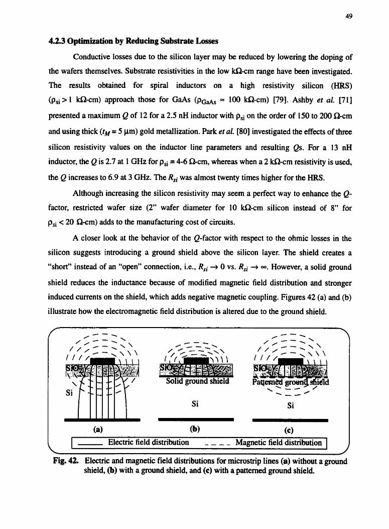
4.2.3 Opamizatîon by Reduchg Subskrate Losses
Conductive losses due to the silicon layer may be reduced by lowering the doping of
the wafers themselves. Substrate resistivities in the low W c m range have ken investigated.
The results obtained for spiral inductors on a high resistivity silicon (HRS)
(psi > 1 D c m ) approach those for GaAs (pGAs 100 kRcm) [79]. Ashby et al. [71]
presented a maximum Q of 12 for a 2.5 nH inductor with psi on the order of 150 to 200 Ckm
and using thick (tM = 5 pm) gold metailization. Park et al. [80] investigated the effects of three
silicon resistivity values on the inductor line parameters and resulting Qs. For a 13 nH
inductor, the Q is 2.7 at 1 GHz for psi = 4-6 Sbcm, whereas when a 2 kR-cm resistivity is used,
the Q increases to 6.9 at 3 GHz. The R, was almost twenty times higher for the HRS.
Although increasing the silicon resistivity rnay seem a perfect way to enhance the Q-
factor, restricted wafer size (2" wafer diameter for 10 k k m silicon instead of 8" for
psi < 20 a m ) adds to the manufacturing cost of circuits.
A closer look at the behavior of the Q-factor with respect to the ohmic losses in the
silicon suggests introducing a ground shield above the silicon layer. The shield creates a
"short" instead of an "open" connection, i.e., Ri + O vs. Ri + m. However, a solid ground
shield reduces the inductance because of modified magnetic field distribution and stronger
induced currents on the shield, which adds negative magnetic coupling. Figures 42 (a) and (b)
illustrate how the electromagnetic field distribution is altered due to the ground shield.
Solid ground shield
1 Electric field distribution - - - - Magnetic field distribution 1
Fig. 42. Electric and magnetic field distributions for microstrip Iines (a) without a growid shield, (b) with a ground shield, and (c) with a patterned ground shield.

Designing a patterned ground shield with narrow
slots, such as the one shown in Fig. 43, minirnizes the
electric field petration into the silicon, but does not
significantly aiter the magnetic fields (Fig. 42 (c)).
Reduction of the line inductance due to the induced
currents on the shield is minirnized by using a thinner metal
layer. The order of the metal thickness must be smaller than
the skin depth of the metal at the operating frequency. A
comparison between 0.5 pm alurninum (ps = 64 mapm)
and doped polysilicon shields (ps = 12 a-pm) for an 8 nH
/ Slot Strip
Fig. 43. Pattemed ground shield.
inductor on an 1 1 R-cm substrate showed a greater peak Q for the polysilicon (20% for polySi
vs. 13% for Al) than without metal ground shields. The measured substrate loss element R, of
the compact model in Fig. 20 increased more than ten times. However, a higher shunt parasitic
capacitance results because the electric field does not penetrate into the silicon, so that only
C,, is taken into account in the inductor model. Hence, a faster Q roll-off after the peak
ensues, and the inductor self-resonance occurs earlier, at 3.6 GHz instead of ai 6.5 GHz [29].
Another approach is to selectively remove the underlying silicon substrate using a
post-fabrication wet [81] or gaseous etch [82] to reduce the parasitic capacitances of the
substrate (Fig. 44 (a)). The "suspended" inductor provides a higher self-resonance: for a
100 nH inductor, the self-resonant frequency increases from 800 MHz to 3 GHz [8 1 1. Other
micro-machining techniques consist of etching the silicon substrate undemeath the structure,
which lies on a 1-2 pm thick dielectric membrane, as shown in Fig. 44 (b). For a 1 nH spiral
inductor layout, the self-resonant frequency increases from around 20 GHz to a maximum of
Fig. 44. Removal of substrate parasitics by (a) selective etching of the underlying silicon, (b) fabrication of a dielectric membrane, or (c) etching part of oxide and silicon layers.
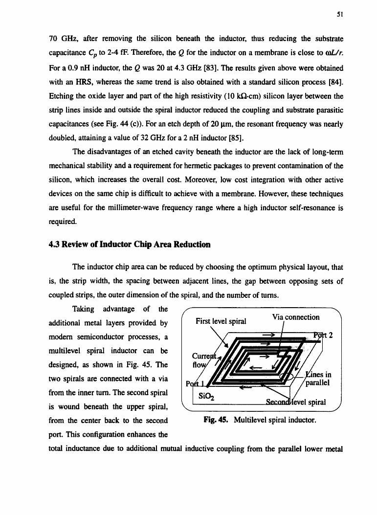
70 GHz, after removing the silicon beneath the inductor, thus reducing the substrate
capacitance Cp to 2-4 fF. Therefore, the Q for the inductor on a membrane is close to W r .
For a 0.9 nH inductor, the Q was 20 at 4.3 GHz [83]. The results given above were obtained
with an H R S , whereas the same trend is also obtained with a standard silicon process [84].
Etching the oxide layer and part of the high resistivity (10 k k m ) silicon layer between the
strip lines inside and outside the spiral inductor reduced the coupling and substrate parasitic
capacitances (see Fig. 44 (c)). For an etch depth of 20 Pm, the resonant frequency was nearly
doubled, attaining a value of 32 GHz for a 2 nH inductor [Ml.
The disadvantages of an etched cavity beneath the inductor are the lack of long-term
mechanical stability and a requirement for hermetic packages to prevent contamination of the
silicon, which increases the overdl cost. Moreover, low cost integration with other active
devices on the same chip is difficult to achieve with a membrane. However, these techniques
are useful for the millimeter-wave frequency range where a high inductor self-resonance is
required.
4.3 Review of Inductor Chip Area Reduction
The inductor chip area can be reduced by choosing the optimum physical layout, that
is, the strip width, the spacing between adjacent lines, the gap between opposing sets of
coupled strips, the outer dimension of the spiral, and the number of tums.
Taking advantage of the
additional metal Iayers provided by
modem semiconductor processes, a
multilevel spiral inductor can be
designed, as shown in Fig. 45. The
two spirals are connected with a via
from the inner tum. The second spin1
is wound beneath the upper spiral,
from the center back to the second
port. This configuration enhances the
/
First level spiral Via connection I
Si% >dvel spiral
Fig. 45. Multilevel spiral inductor.
total inductance due to additional mutual inductive coupling from the parailel lower metal

strips. To maintain a reasonable series resistance, the lower metals can be stacked. However,
separation between the lowest metal layer and the oxidelsilicon boundary results in severe
degradation of the Q-factor, due to higher oxide and line-to-line coupling capacitances.
Table 4 compares the line parameters and Q-factors for two 4 tum inductors connected
in series with a parallel connected spiral as in Fig. 45, for which the overall chip area was
reduced by one half. Thus, for the same series resistance, the inductance increased by 70%,
whereas the Q decreased by 35%. Resulting €rom the higher parasitic capacitances, the self-
resonant frequency aiso decreased substantially. For an equal chip area as the parallel
connected inductor, an 8 turn 9 nH inducior shows a better performance than the parallel
inductor. Although the series resistance is almost double, the influence of the capacitive
parasitics is less pronounced [12]. Therefore, this chip area reduction technique is uscful for
obtaining higher inductances, at the expense of higher parasitic capacitances which degrade
the overall performance of the inductor.
Table 4. Cornparisons with senes and pardlel connected inductors [12].
4.4 Proposed Method
Inductive loads are widely used in RF circuits, such as amplifiers, oscillators and
mixers. Circuit performance depend on the quality of the components used. These influence
the circuit's linearity, total noise level, and power consumption. In the previous section,
various Q-factor enhancement techniques were presented. Without altering the fabrication
process, a new inductor design is proposed that is suitable for differential circuits (which are
one of several existing RF design topologies).
fped (GB)
2.4
1
1.8
L
Inductor L
Series
Parallel
Single
L (nH)
5.2
8.8
I
/,(GHz)
18.3
3.3
, 9.1
N t u m
4
4
r (R)
5
5
I 9.5
Qped
10.4
6.8
9.5
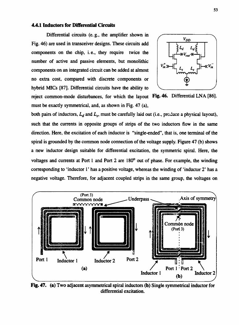
4.4.1 Inductors for Düîerential Circuits
Differential circuits (e. g., the amplifier show in
Fig. 46) are used in transceiver designs. These circuits add
components on the chip, i.e., they require twice the
number of active and passive elements, but monolithic
components on an integrated circuit can be added at almost
no extra cost, compared with discrete components or
hybrid MICs [87]. Differential circuits have the ability to
reject comrnon-mode disturbances, for which the layout
must be exactly symmetrical, and, as shown in Fig. 47 (a),
Fig. 46. Differential LNA [Ml.
both pairs of inductors. Ld and L,, must be carefully laid out (i.e., pr~Uuce a physical layout),
such that the currents in opposite groups of strips of the two inductors Row in the same
direction. Here, the excitation of each inductor is bbsingle-ended", that is, one terminai of the
spiral is grounded by the common node connection of the voltage supply. Figure 47 (b) shows
a new inductor design suitable for differential excitation. the symmetric spiral. Here, the
voltages and currents at Port 1 and Port 2 are 180' out of phase. For example, the winding
corresponding to 'inductor 1 ' has a positive voltage, whereas the winding of 'inductor 2' has a
negative voltage. Therefore, for adjacent coupled strips in the same group, the voltages on
(Port 3) Common node 3YYr(rY*IYrll/
Under
Port 2
pass -
i
\ , Axis of symmetq
/ port1;port2 \ Inductor 1
(a) Inductor 2
Fig. 47. (a) Two adjacent asymmetrical spiral inductors (b) Singie symrnetrical inductor for differentid excitation.

each strip are out of phase, but the current flow is in the same direction. Whereas for each
conventional inductor in Fig. 47 (a), the voltages on adjacent strips of the same group have a
small phase lag between each other, and hence, inductors 1 and 2 cannot be differentially
excited.
4.4.2. Asymmetricd vs. Symmetrical Inductors
A conventional inductor is wound into a spiral to reduce space and uses an underpass
or crossover to the inner node to facilitate connections to other circuitry. The symmetrical
inductor is designed by joining groups of coupled strips from one side of the axis of symmetry
to the other, using underpasses. This idea was first applied to transformers for coupling both
primary and secondary coils [88].
The symmevical inductor layout has many advantages. 'Ibo separate spirals are
replaced by a single coil, and the common node separates the spiral to form two equal
inductances. Substrate parasitics are the sarne at either port. For a pair of asymmetric
inductors (see Fig. 47 (a)), a finite spacing between both inductors must be maintained to
reduce negative coupling; this is not an issue for symrneuical inductors. Moreover, a reduction
in chip area results. The example in Fig. 47 shows two 4 nH conventional spiral inductors and
an 8 nH symmetric inductor, for which a 35% area reduction results. Since both ports are
adjacent, the syrnmetric inductor is suitable for the connection to active devices, such as
transistors,
4.5 One-Port Excitation Theoretical Analysis
As an aid to qualitative understanding of the single-ended and differential one-port
excitations, Fig. 48 illustrates the various currents flowing on the conductor and in the
substrate of a microstrip line on silicon. Conduction cumnts are present on the line conductor
as Ic,, and in the silicon substrate as Ics. The displacement current b flows within the
substrate layers to reach the gmund plane. The difference between singleended and
differential excitations lies in the current renirn paths. In the differential case, the substrate
currents retum to the lower potential node. The physical interpretation of this phenomenon
will be translated into an equivalent circuit.
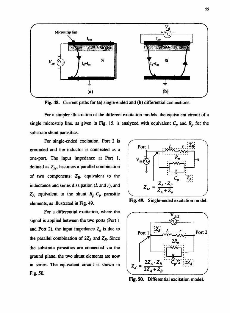
Microstrip line
Fig. 48. Current paths for (a) single-ended and (b) differentiai connections.
For a simpler illustration of the different excitation models, the equivalent circuit of a
single microstrip line, as given in Fig. 15, is anaiyzed with equivalent Cp and Rp for the
substrate shunt parasitics.
For single-ended excitation, Port 2 is
grounded and the inductor is connected as a
one-port. The input impedance at Port 1,
defined as Z,, becomes a parallel combination
of two components: ZB, equivalent to the
inductance and series dissipation (L and r), and
2'' equivalent to the shunt Rp-Cp parasitic
elernents, as illustrated in Fig. 49.
For a differential excitation, where the
signal is applied between the two ports (Port 1
and Port 2), the input impedance Zd is due to
the parallel combination of 2ZA and Zg. Since
the substrate parasitics are connected via the
ground plane, the two shunt elements are now
in series. The equivalent circuit is shown in
Fig. 50.
Fig. 49. Single-ended excitation model.
Port 2
J
Fig. 50. Differentiai excitation model.

With a higher substrate shunt impedance for the differential case, Zd approaches the
value of ZB, over a higher range of frequencies than for 2,. In other words, at lower
frequencies, the input impedance in either the shunt or the differential connections is
approximately the same, but as the frequency increases, the substrate parasitics, Cp and Rp,
corne into play. For the differential excitation case, these parasitics have a higher impedance at
a given frequency than in the single-ended connection. This reduces the real part and increases
the reactive component of the input impedance. Therefore, the inductor Q is improved when
driven differentiaily, and moreover, a wider operating bandwidth can be achieved at no extra
processing cost.
4.6 Test Structure
A 5 tum square symmetric spiral inductor was fabricated and tested in order to verifj
the above predictions. The outer dimension OD, as shown in Fig. 51 (a), is 250 Pm; the strip
line is 8 pm wide, and the spacing s between conductors is 2.8 Pm. The inner gap between
opposite groups of coupled lines is approximately 150 Pm, which minimizes negative mutual
coupling, whereas the relatively narrow conductor width and spacing results in higher positive
Port 1 / . /
Ground 1 1 \
Passivation s w
(a) Fig. 51. (a) Inductor test structure layout. (b) Partial cross-sectionai view of the inductor.

magnetic coupling and lower substrate capacitive parasitics. The inductor consists mainly of
top metal (M3), and the second level metal (MZ) is used for the underpasses. Both signal and
ground pads are located on the same side; thus a set of probes with two adjacent RF contacts
was used. A cross-sectional view of a portion of the structure is illustrated in Fig. 51 (b).
(Properties of the substrate and the alurninum alloy metal for the fabrication process [89] are
listed in Table 5.) For de-embedding purposes [go], shon and open structures or "dummies"
were also fabricated, as shown in Fig. 52.
Table 5. Substrate and metal panmeters.
I Parameter I Value I 1 Oxide thickness ;ver M2 1 h3 - h6- 1 Oxide thickness below M2 1 h2 = 3.61 pm 1 1 Silicon resistivity 1 psi = 15 R-cm
1 Silicon thickness 1 h l =200pm 1 - - - 1 Top metal M3 resistivity / p~ = 3 1 ma-pm 1
1 M3 thickness 1 h5 = 2.07 prn 1 1 M2 thickness 1 h6 = 0.84 prn - 1
Fig. 52. Open and short dummies for the inductor in Fig. 51 (a).
4.7 Symmetric Inductor Modeiing
The modeling procedure for the symmetric inductor foiiows that of Chapter 3.
Figure 53 gives an exampie for N = 3. For the inductance value, Greenhouse's method is
applied, considering six groups of coupled strips instead of four for a conventionai spiral. This

- -- -
Fig. 53. 3 turn symmetric inductor modeling with (a) group sectioning and (b) line-to-line capacitances.
results in a total of 6N line segments, where N is always an integer. Positive mutual
inductances are cakulated for each group, whereas negative mutual inductances are obtaimd
with respect to Group 2 and Group 5, Group 3 and Groups 1 and 6, and Group 4 and Groups 6
and 1, as shown in Fig. 53 (a). These mutual inductances are doubled since the inductor
geornetry is symmetric. Self-inductances for extra connections, i. e., the under and overpasses,
which are not included in the groups, are added, but these are negligible (for a typical 20 pm
long microstrip line, the inductance is less than 0.05 nH). Rd, takes into account the total
length of the syrnmetric structure, including the underpasses, and the different metallization
thicknesses and sheet resistivities. The total substrate capacitances C,, and Ck are derived in
the sarne manner as described in Section 3.2.3. The overall capacitance Co is a combination of
underpass capacitances Cu and interwinding capacitances. As shown in Fig. 53 (b), the
combination diffea €rom the asymmetric inductor, but the optirnization method described in
Chapter 3 is sirnilarly applied to the symmetric inductor. The final model is also distributed
into a maximum of 4N sections, defined in Section 3.2.5.
Table 6 sumrnarizes the element values found for the 4 mm long structure shown in
Fig. 5 1 (a). The optimized model of Fig. 54 compares well with the values obtained by fitting
the simulated and measured data over a frequency range of 0.5 to 6 GHz (below self-

59
resonance). Since the inductor structure is syrnrnetrïc, substrate parasitics should be the same
at both ports.
Table 6. Lumped elernent values for the 5 tum symmetric inductor.
I I
I \ (8.3) ( 7-9)
Port 1 L=7 .8nH r = 7 . 8 Q Port 2 O I I
O
Fig. 54. Parameter fit circuit mode1 for measured and (simulated) symmetrhc inductor.
4.8 Memurement Procedure
The symmetric inductor in Fig. 51 (a) was charactenzed
experimentally from on-wafer measurements using a two-port
vector network analyzer and Picoprobe 40A-GS- 150-DUAL RF
probes. The probes, manufactured by GGB Industries, consists of
two signal-ground coaxial probes mounted on a single base, as
illustrated in Fig. 55. The spacing between the ground G and
signal S fingers is 1 50 pm [9 1 1.
/ \ Probe 1 Probe 2
S G S A
Fig. 55. Dual probes. 4m8.1 Calibration
First, the calibration specifications for the probes provided by the manufacturer are
entered into the network analyzer. Second, an impedance standard substrate (ISS) [92] is used
for the short, open, load, and thru (SOLT) hi11 2-port caiibration. During caiibration, Probe 1
of the set of duai probes is positioned on a holder opposite Probe 2. After calibration, it is
moved back to the same probe head, as shown in Fig. 55. This extra step may add some error
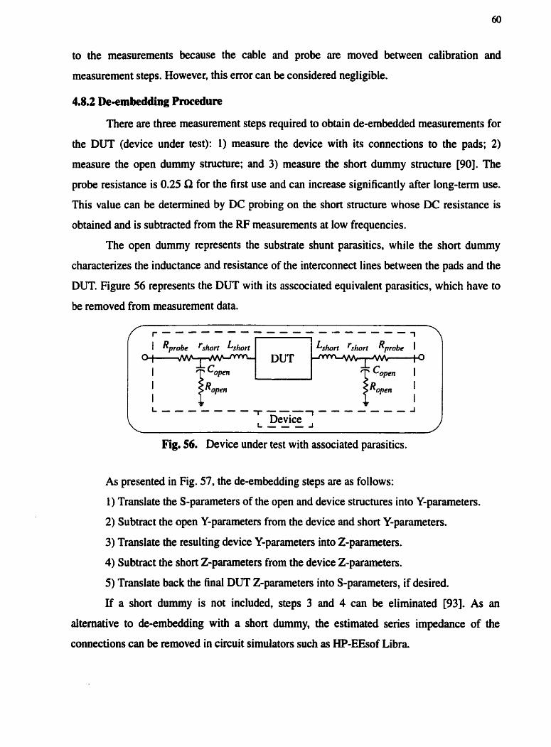
to the measurements because the cable and probe ûre moved between cdibration and
measurement steps. However, this error can be considered negligible.
4.8.2 De-embedding Procedure
There are three measurement steps required to obtain de-embedded measurements for
the DUT (device under test): 1) measure the device with its connections to the pads; 2)
measure the open dummy structure; and 3) measure the short dummy structure [90]. The
probe resistance is 0.25 R for the first use and c m increase significantly d e r long-terni use.
This vaiue can be determined by DC probing on the short structure whose DC resistance is
obtained and is subtracted from the RF measurements at low frequencies.
The open dummy represents the substrate shunt pansitics, while the short dummy
characterizes the inductance and resistance of the interconnect lines between the pads and the
DUT. Figure 56 represents the DUT with its asscociated equivalent parasitics, which have to
be removed from measurement data.
1 Rprnbc 'short Lshort Lrhort 'short Rprobc 1 DUT 1
14
Fig. 56. Device under test with associated parasitics.
As presented in Fig. 57, the deembedding steps are as follows:
1) Translate the S-parameters of the open and device structures into Y-parametea.
2) Subtract the open Y-parameters from the device and short Y-parameters.
3) Translate the resulting device Y-parameters into 2-parameters.
4) Subtract the short 2-parameters €rom the device 2-parameters.
5 ) Translate back the final DUT 2-parameters into S-parameters, if desired.
If a short dummy is not included, steps 3 and 4 can be eliminated [93]. As an
alternative to de-embedding with a short dummy, the estimated series impedance of the
connections can be removed in circuit simulators such as HP-EEsof Libra.

Fig. 57. Flowchart of de-embedding steps.
4.8.3 Single-ended vs. Differential Parameters
Single-ended and differentid
configurations are derived from the two-port
measurements, as shown in Fig. 58. The one-port
S-parameters are expressed as the two-port
network equivalent incident and reflected
signals, as described below:
bl = Sl Pl +S12a2
b2 = S 2 P l +Sua2
Fig. 58. Two-port S-matrix with both configurations.
' ik Er& where ak = - and bk = - with k = 1,2; Ei and Er are the incident and reflected waves, 4E JZ
respectively, and 2, is the system impedance (50 R). For the single-ended configuration,
Ei2 + Es = O or a2 = -& (with Port 2 grounded), and hence the following equation is obtained
from (23) for the one-port S-parameter S,,:
The difference between the first and second equations of (23) gives the differential signal. i.e.,
Erd8= bl - b2. In this case, Eil + E2 = O or ai = -az, such that an equivalent incident signal
Ci de fines the differentiai one-port S-parameter Sd as
The second approach consists in deriving Y
, - - - - * * - - -
Vd the input impedance directly from the transformed @ O - - - - - - - - *.
0
1 1 r
2-port 2-matnx (Fig. 59). which is related to the
port voltages and currents by the following
expressions:
(*@ Fig. 59. Two-port 2-rnatnx with both configurations.
With Pon 2 grounded, the single-ended
configuration implies that V2 = O, so that the input impedance becomes
For the differential case, Vd = VI - V2 is the resulting signal voltage, with I2 = -Il. Thus the
input impedance is
where 22, is obtained from the differential system impedance.
The two-port symmetric spiral inductor was simulated using HP-Momentum, for
which the spacing between adjacent lines was taken as 3 pm instead of the 2.8 pm specified in
the design. The structure was simulated from 500 MHz to 6 GHz in steps of O S GHz.

Measurements performed on the HP 8753D network anaiyzer ranged from 10 MHz to 6 GHz,
and those on the HP 8722C, from 500 MHz to 20 GHz. Measured and simulated structures
were properly de-embedded with the open and short dummies. The probe resistance was
estimated to be around 0.3 R. Three sets of measurements were performed with different
calibrations. Caiibrations A and B were done with the HP 8753D for which 4 and 11 test
samples, respectively, were measured, and calibration C on the HP 8722C used 4 test samples.
4.9.1 Parasitics
With an estirnated probe resistance of 0.3 R, measured and simulated short
interconnections had a 250 pH inductance in series with a 0.1 to 0.4 R frequency dependent
resistance. Theoretical values for Lsh were found to be 220 pH and for ',hort, 0.25 R. Shunt
parasitic values at 2 GHz for the open structure are shown as histograms in Fig. 60. Depending
on the calibntion, different values were obtained. Sirnulated results gave a 5 1 tF capacitance
in series with a 46 1 R resistance.
Crilibration A
Calibration B
Calibntions A, B. and C
Fig. 60. Open dummy structure parasitic histograms over 15 samples.
4.9.2 Results and Discussion
Figure 61 (a) shows the measured inductance and series resistance of the spiral
inductor structure after de-embedding. These values were taken at 500 MHz, for a low
frequency parameter extraction from the input impedance. Inductance values are more
sensitive to the accuracy of the calibration performed. whereas the resistance fluctuates
between 7.3 R and 8.8 Q. For repeatability comparisons, some measurements were done on
the same inductor using different calibrations. These results show that the values depended on
the calibration and not on the chip itself. Sirnulated results gave a total inductance of 8.3 nH
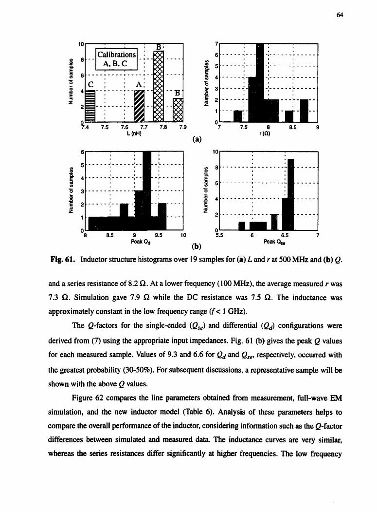
Calibrations : A,B,C l-:
8.5 9 9.5 Peak Qd
O 5.5 6 6.5 7
(b) Peak Q,,
Fig. 61. Inductor structure histograms over 19 samples for (a) L and r at 500 MHz and (b) Q.
and a senes resistance of 8.2 R. At a lower frequency (100 MHz), the average measured r was
7.3 R. Simulation gave 7.9 R while the DC resistance was 7.5 R. The inductance was
approxirnately constant in the low frequency range (f< 1 GHz).
The Q-factors for the singleended (Qse) and differential (Qd) configurations were
derived from (7) using the appropriate input impedances. Fig. 6 1 (b) gives the peak Q values
for each measured sample. Values of 9.3 and 6.6 for Qd and Qse, respectively, occurred with
the greatest probability (30-50%). For subsequent discussions, a representative sample will be
shown with the above Q values.
Figure 62 compares the line parameters obtained from measurement, full-wave EM
simulation, and the new inductor mode1 (Table 6). Analysis of these parameten helps to
compare the overall performance of the inductor, considering information such as the Q-factor
differences between simulated and measured data. The inductance curves are very similar,
whereas the series resistances differ significantly at higher frequencies. The low frequency

substrate capacitance gives the oxide capacitance value. The measured data shows a large
error in this range.
S t O 2 4 6
Frequency (GHz)
U
O 2 4 6 Frcquency (GHz)
300
O 2 4 6 2 o o , ; i $ ; , Frqucncy (GHz) Frequcncy (GHz)
Fig. 62. Transmission line equivalent parameters for the 8 nH symmetric inductor.
A cornparison between the experimental measurements, full-wave EM simulation, and
the new inductor model for the input impedance and the Q-factor are shown in Figs. 63 and
64. At lower frequencies, the difference in Q between the differential and single-ended
excitations is not significant (4 %) because the shunt capacitive parasitic components do not
affect the low frequency input impedance. Hence, the two cases can be represented by a series
L-r model. However, as the frequency increases, the difference between the input impedances
becomes substantiai: Zd is much lower than 2' by an increasing factor. This is caused by the
lower substrate parasitics present in the differentially excited case, as previously described. As
shown in Fig. 64, the difference between Q-factors in the differential and single-ended cases
illustrates this point. The peak in the Q-factor is a result of the shunt parasitics resonating with
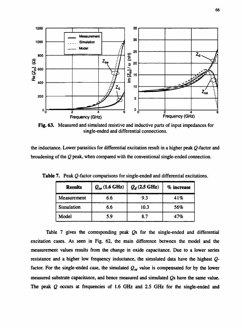
Frequency (GHz) ~requency (GHz)
Fig. 63. Measured and simulated resistive and inductive parts of input impedances for single-ended and differential connections.
the inductance. Lower parasitics for differentid excitation result in a higher peak Q-factor and
broadening of the Q peak, when compared with the conventional single-ended connection.
Table 7. Peak Q-factor cornparisons for singleended and differential excitations.
Table 7 gives the corresponding peak Qs for the single-ended and differential
excitation cases. As seen in Fig. 62, the main difference between the model and the
measurement values results from the change in oxide capacitance. Due to a lower series
resistance and a higher low frequency inductance, the simulated data have the highest Q-
factor. For the single-ended case, the simulated Qse value is cornpensated for by the lower
measured substrate capacitance, and hence measured and simulated Qs have the same value.
The peak Q occurs at frequencies of 1.6 GHz and 2.5 GHz for the single-ended and
Simulation
Mode1
6.6
5 ,9
10.3
8.7
56%
47%
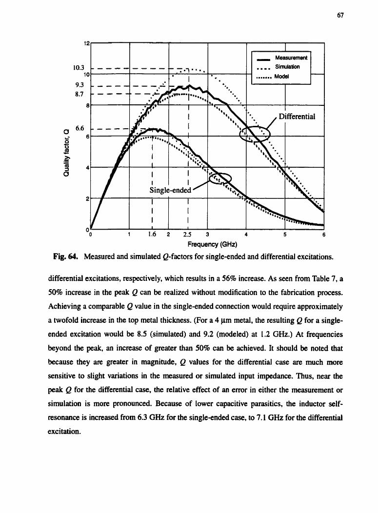
"O 1 1.6 2 2.5 3 4 5 6
Frequency (GHz)
Fig. 64. Measured and simulated Q-factors for single-ended and differential excitations.
differential excitations, respectively, which results in a 56% increase. As seen from Table 7, a
50% increase in the peak Q can be realized without modification to the fabrication prmess.
Achieving a comparable Q value in the single-ended connection would require approximately
a twofold increase in the top metal thickness. (For a 4 pm metal, the resulting Q for a single-
ended excitation would be 8.5 (sirnulated) and 9.2 (modeled) at 1.2 GHz.) At frequencies
beyond the peak, an increase of greater than 50% can be achieved. It should be noted that
because they are greater in magnitude, Q values for the differential case are much more
sensitive to slight variations in the measured or simulated input impedance. Thus, near the
peak Q for the differential case, the relative effect of an e m r in either the measurement or
simulation is more pronounced. Because of lower capacitive parasitics, the inductor self-
resonance is increased from 6.3 GHz for the single-ended case, to 7.1 GHz for the differentiai
excitation,

4.93 Sources of Error
As previously discussed, calibration. de-embedding structure parasitics, and probe
contact resistance are al1 sources of error that can alter the measured DUT parameter values.
Inaccuracies due to imperfections in the connectors, cables, temperature and frequency drifts
within the network analyzer, calibration, and test devices add to the random measurement
errors [94].
Other errors are caused by variations in the fabrication process. An important factor is
the top metal thickness, which cm vary within f 10%. After a 10% increase in the metal
thickness, Rd, is 6.8 R, and the simulated series resistance becomes 7.6 R at 500 MHz,
compared with the measured value of 7.7 R. For a submicron IC process, the metal lines are
defined photolithographically to within 0.1 pm, which has a negligible effect on the line
inductance and resistance. Simulations were performed for a k0.2 pm strip width variation,
and no significant changes (< 2% in the peak Q) were observed. For a k 1 pm change in oxide
thickness and a f 50% change in silicon resistivity, simulations also predict a f 5% variation in
the self-resonant frequency and in the peak Q.
Inaccuracies in the electromagnetic simulation are mainly caused by improper
rneshing of the structure which is a contributing factor to an approximation of the actual
device. Moreover, present simulators do not account for variations in temperature of the metal
in a spiral inductor.
4.9.4 Optimized Equivalent Circuit Models
Figure 65 shows a lumped-element
model for the symmetric inductor that was fit
numerically over a broad band of frequencies
(0.5-6 GHz) for both the single-ended and
differential connections. Tables 8 and 9 give
the element values for measured and simulated
results. Here, L is the low frequency
inductance, and r is the series resistance at
\ - Single-ended . --- . Differentid
I Port 2 n, Cl =2
Fig. 65. Optirnized equivalent circuit model for both configurations.
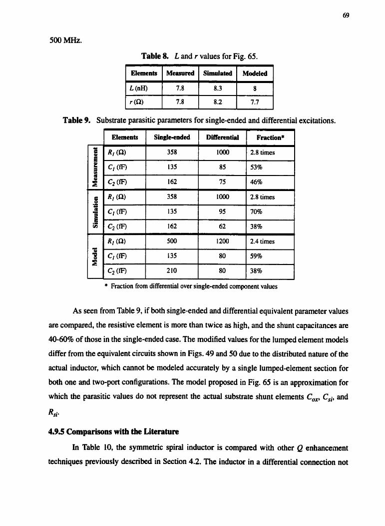
500 MHz.
Table 8. L and r values for Fig. 65.
Table 9. Substrate parasitic parameters for single-ended and differential excitations.
* Fraction from differential over single-ended component values
As seen from Table 9, if both single-ended and differential equivalent parameter values
Elements - Y
3 RI (fi) E
are compared, the resistive element is more than twice as high, and the shunt capacitances are
4060% of those in the single-ended case. The modified values for the lumped element models
Single-endeà
358
135
162
358
135
162
500
135
2 10
differ from the equivalent circuits shown in Figs. 49 and 50 due to the distributed nature of the
CI ml c2 (@
RI (fi)
Cl (tF)
C2 (fF)
RI (fi>
c m
c2 (fF)
I 2
actual inductor, which cannot be modeled accurately by a single lumpedelement section for
Differential
IO00
85
75
IO00
95
62
1200
80
80
,
both one and two-port configurations. The mode1 proposed in Fig. 65 is an approximation for
Fraction*
2.8 times
53%
46% I
2.8 cimes
70%
38%
2.4 times
59%
38%
I i;;
9
3 E ,
which the parasitic values do not represent the actual substrate shunt elements C,, Csi, and
4.95 Cornparisons with the Litenaire
In Table 10, the symmetric spiral inductor is compared with other Q enhancement
techniques previously described in Section 4.2. The inductor in a differential connection not

only has a higher Q-factor, but also can be implemented in al1 of the aforernentioned
technologies to further enhance the overall Q and obtain an even broader bandwidth.
Table 10. Cornparisons of published references with the differential symmetric inductor.
4.10 Application
This section describes a circuit application incorporating monolithic inducton.
Inductors can be used as tuned loads or feedback elements in differential circuits such as
amplifiers, oscillators, and mixers.
For the purpose of this thesis, the 8 nH symmetnc inductor will be incorporated into an
oscillator designed for the 2.4-2.48 GHz ISM band WLAN market. The intermediaie
frequency IF for this application is specified at around 350 MHz. Therefore, a local oscillation
frequency of 2.05 to 2.1 GHz is required. First, a Colpitts oscillator is used to show the
implementation of the inductor in a single-ended connection. The oscillator performance is
compared using measured and simulated data, and the new inductor model. Second, a
differential version of the Colpitts as a cross-coupled oscillator will illustrate the advantages
of the symmetric inductor over the integration of two identicai asyrnrnetric inductors.
Inductor type I
1-level metd
2 stacked metais I
3 stacked metais
4.10.1 OsriHator Design
For an oscillation to occur, a resonator, consisting of an inductor in shunt with a
capacitor (and their associated parasitics), is connected to an active circuit, as shown in
Fig. 66. For sustained oscillation, the na1 part of the impedance seen looking into the active
Reference
Long 1251
Park [80]
Burghartz 1771
psi (hm)
10
2 k
12
10-20
2 k
10 k
15
tM @m)
1 -3
2
4.3
2
1 (Au)
2
Ground shield
Membrane
1
Etched oxide/Si r
Differentid Single-ended
Yue [29]
Chi [83j
Rieh [85]
Danesh / Long
L (dl)
1.88
13
2.2
8
0.9 1.2
2
8
f&d
6-10@4GHz
12 @ 3 GHz
l 6 @ 2 G H z
7.2 @ 1.5 GHz
20 @ 4.3 GHz A,: 70 GHz
f,,: 30 GHz I
9.3 @ 2.5 GHz 6.6 @ 1.6 GHz

circuitry must be a negative resistance -R that is equal to or less than the Req of the resonator.
The frequency of oscillation, determined by the resonance frequency of the LC tank, is given
approximately as
Resonato r -R . - - - - - - - - - - - . I
Active circuit
. - - - - - - - - - - - a
Fig. 66. (a) LC tank and (b) equivalent resonator in a one-port oscillator.
4.10.2 Colpitts Oscillator
The Colpitts oscillator is the most commonly used design because only one inductor is
needed. Moreover, incorporating one active device into the circuit minimizes the noise
sources. The Colpitts oscilliitor shown in Fig. 67 uses collecter to emitter feedback. At
* Fig. 67. Colpitts oscillator circuit.

resonance, the impedance of the resonator is real. The total phase shift of the signal fed back
from the collector to the emitter is zero. The LC tank shown in Fig. 67 consists of an 8 nH
symmetnc inductor in parallel with CI and C2 in series. Here, RL is the load due to another
circuit such as a mixer in a wireless transceiver, and BJTz provides the bias current for the
oscillator.
a) Operating Points
Wtth a 3 V supply, the DC voltage at the collector of BJTl is also 3 V. For transistor
BJT2 to be in the forward active region, its collector voltage must be higher than 0.9 V
because the base-ernitter voltage Vbe is approximately 0.9 V. The voltage at the base of BJTl
Vbbl is Vbe+IbiasRE Therefore, the voltage at the base of BIT 1 shouid be between 1.8 V and
3 V, depending on the values of rbias and RE.
For an oscillation to occur at 2.1 GHz with an 8 RH inductor, Ceq must be equal to
0.72 pF, given by (29). However, because of added parasitic capacitances introduced by the
monolithic inductor, a lower Ceq must be chosen. It has been shown that the best phase noise
performance is obtained for the Colpitts with the ratio C2 ICI equal to 4 [95]. Table I 1 gives
the find component and voltage source values. A current bias Ibis of 0.68 mA results, such
that the current Bowing into BJTt is 1.13 mA.
Table 11. Element and source values for the Colpitts oscillator.
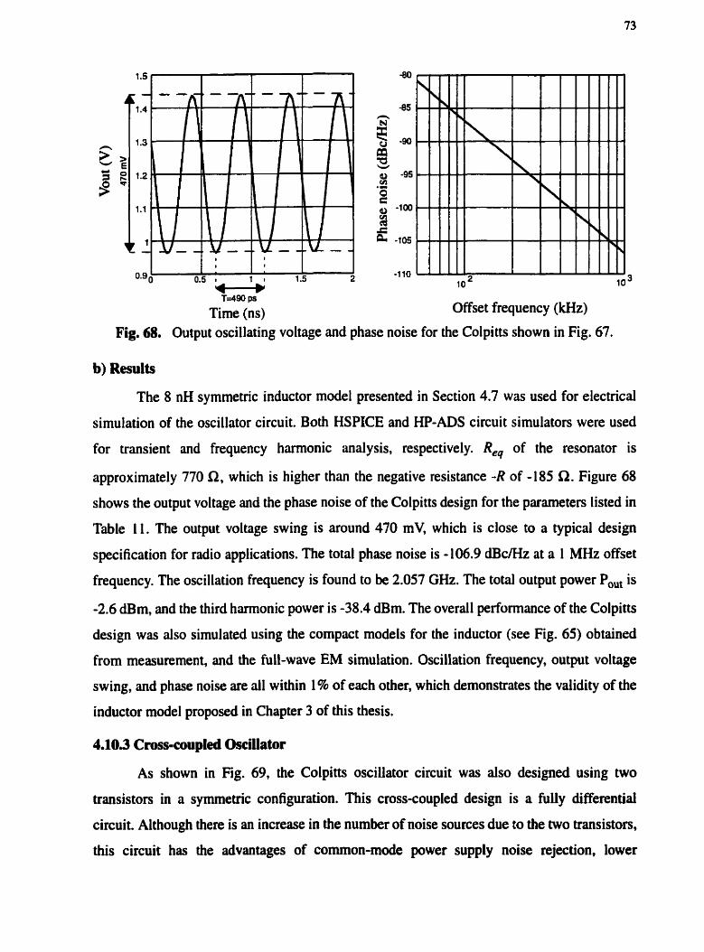
Time (ns)
ia2 10
Offset frequency (kHz)
Fig. 68. Output oscillating voltage and phase noise for the Colpitts shown in Fig. 67.
b) Results
The 8 nH symmetric inductor model presented in Section 4.7 was used for electrical
simulation of the oscillator circuit. Both HSPICE and HP-ADS circuit simulators were used
for transient and frequency harmonic andysis, respectively. Req of the resonator is
approximately 770 R, which is higher than the negative resistance -R of -185 Q. Figure 68
shows the output voltage and the phase noise of the Colpitts design for the parameters lisied in
Table 11. The output voltage swing is around 470 mV, which is close to a typical design
specification for radio applications. The total phase noise is -106.9 clBc/Hz at a 1 MHz offset
frequency. The oscillation frequency is found to be 2.057 GHz. The total output power Po, is
-2.6 dBm, and the third harmonic power is -38.4 dBm. The overall performance of the Colpitts
design was also simulated using the compact models for the inductor (see Fig. 65) obtained
from measurement, and the full-wave EM simulation. Oscillation frequency, output voltage
swing, and phase noise are al1 within 1% of each other, which demonstrates the validity of the
inductor model proposed in Chapter 3 of this thesis.
4.10.3 Cross-cou pled Oseillator
As shown in Fig. 69, the Colpitts oscillator circuit was also designed using two
transistors in a symrnetric configuration. This cross-coupled design is a fuiiy differential
circuit. Although there is an increase in the number of noise sources due to the two transistors,
ihis circuit has the advantages of cornon-mode power supply noise rejection. lower

harmonic generation, and higher output voltage swing. The resonator associated with BJTl
consists of LI, C3, and CI. Capacitors CI and C2 provide regenerative feedback from the
output to the base of B JT and BJT2 [96].
Fig. 69. Cross-coupled oscillator circuit.
a) Operating Points
The supply voltage V,, is chosen to be 3 V for this design. In the forward active region
of BJTs 1 and 2, Vbbl must be less than V,,, but greater than the voltage at the coliector of
B U 3 + Vb, 1,2. The LC tank consists of LI and 2C3. For a resonance to occur at 2.1 GHz, C3
should be approximately 0.72 pF, but due to the effect of CI in the feedback path, C3 must be
reduced in value. Ri and R2 must be large to isolate the voltages at the bases of BJTl and
BJT2 from RF signals. The bias current for each transistor BJTl and BJT2 has k e n chosen to
be the same as in the Colpitts example. Table 12 sumrnarizes the final component values.
Table 12. Component values for the cross-coupled oscillator.
b) Results
The crosscoupled osciliator performance is compared for two different spiral inductor
configurations. As shown in Fig. 47, one design incorporates the two 4 nH conventionai spiral
inductors, and the other, a single 8 nH symmetric inductor. Characteristics of the asymmetric
4 nH spirals and the 8 nH symmetric inductor are given in Table 13. The process parameters
of Table 5 were assumed for both inductors. The spacing between the two 4 nH adjacent
spirals is assumed to be much greater han 40 Pm, so that coupling between the inductors is
minimized. A mode1 for the 4 nH conventional spiral was determined. The 8 nH symmetnc
inductor was excited differentidly whereas the two 4 nH conventional spirals were each
connected in the single-ended configuration, as described in Section 4.4.1.
Table 13. Comparisons between 8 nH symmetric and 4 nH conventional inductors.
C haracteristics symmetr ic ic I 1 4nH I 1 Inner gap 1 15Opm 1 140prn / 1 Total length 1 4 mm 1 2.44 mm 1
For the differential output R of -290 R in the 2 GHz range, Req of the 8 nH symrnetric
inductor is 2 kR, whereas for the 4 nH asymmetric inductor, it is 800 i2 . Figure 70 shows the
differential output voltage and the total phase noise for electrical simulations of the
differentiai oscillator using both inductor configurations. Table 14 compares the performance
of the oscillator with each inductor configuration.

Time (ns)
to2 103
Offset frequency (W)
1 8 nH symmetric inductor - - - - - . Two 4 nH asymmetric inductors 1 Fig. 70. Differential output voltage oscillation and phase noise for the 8 nH symmetric
inductor and two 4 nH asymmetnc spiral inductors.
Table 14. Cornparison of cross-coupled oscillator performance for both inductors.
Parameters symme t i c asymme tric I l InH l
Due to the differences between the series resistance and substrate parasitics for the
conventional spiral and the symmetric spiral, a lower output swing and a poorer phase noise
result. The optimized compact models shown in Fig. 65 for the measured and simulated
symmetric inductors compare within 3% for the overall oscillator penomances.
Chip area is another important issue. As mentioned in Section 4.4.2; the symmetric
inductor reduces the total area by 35% when compared with two 4 nH conventional inductors
with a 40 pm spacing. A differential osciilator, as in [97], could be redesigned using a single

symmetric inductor to realize a substantial reduction in the overall chip ares*
Thus, a symmetric inductor can be excited differentially, and it has been shown that
this results in a higher peak Q-factor. Moreover, a single symmetric inductor cm replace two
conventional singlecnded spirals to improve electricai performance and Save chip area. The
oscillator described in this chapter performed better with the single symmetric inductor than
with two asymrnetric spirais.
Chapter 5
CONCLUSIONS
This thesis examines single and coupled microstrip transmission lines on silicon
dioxide/silicon substrates and the spiral microstrip inductor. A basic understanding of the
electrical behaviour of the microstrip line required representations of the electromagnetic field
propagation. Current silicon processes have low to medium resistivities which considerably
influence the behaviour of the fields in the substrate, and hence, the charactenstics of the strip
line. These propagation modes are defined by the quasi-TEM, slow-wave, and skin-effect
modes. For typicd bipolarKMOS processes, the slow-wave mode and transitions from the
slow-wave to quasi-TEM or skin-effect mode regions are the most common in the low GHz
frequency range.
Lumped element equivalent circuits are required to model rnicrostrip structures in
circuit simulators such as SPICE. The model used in this thesis is a x-type lumped element
equivalent circuit. Closed-form expressions for the inductance and series conductor resistance
are utilized in the model, in which the inductance is considered to be a constant, and the series
resistance is a frequency dependent parameter that takes the skin-effect and the conductive
silicon effect into account. For deriving the substrate pansitics, that is, oxide and silicon
capacitances, and conductive substrate resistance, several methods have been proposed in the
literature, most of which use static approximations. The single microstrip line model agreed to
within 5% of the simulated Q-factor results. The influences of dl the lumped elemenis with
respect to the substrate resistivity and line widths were discussed.
Analysis of single microstrip lines provided the underlying basis upon which a model
for spiral inductors was developed. Several inductor modeling techniques have k e n
previousiy reported in literature, however, in this thesis, a simpler method was presented. This
inductor mode1 extends die pinciples of the single rnicrostrip line model to groups of multiple
coupled lines that form a spiral inductor. Transmission line parameters and the resulting
inductor Q-factor compared well with the measured data for conventional spüais fabcicated in
various processes for a range of physical layouts. Moreover, this mode1 can be easily
integrated into an RF circuit simulator.

Symmetric differential circuits are one of the existing topologies used in amplifiers,
mixers, and oscillators that implement spiral inductors. Current differential circuits use two
spiral inductors placed adjacent to each other in the physical layout. A single symmetric
inductor can replace both conventional asymrnetric spirals in a differential connection. The
total chip area is reduced when a symmetric circuit layout is used. Moreover, the symmetric
inductor geometry is better suited for interconnection with other components, such as
transistors, which are usually smaller in size.
The primary benefit of differentially excited inducton is that they are less affected by
substrate parasitics. Therefore, resulting Q-factors are higher than in the single-ended case.
For a 5 tum, 8 nH symrnetric inductor, it was shown that the peak Q increases by 50% and
even more after the peak frequency. The inductor self-resonant frequency also increases by
about IO%, and a broder operating bandwidth for the differentially excited inductor is
achieved. A model for the symmetric inductor, based on the conventional spiral inductor
model, was also developed. The symmetric inductor models were validated using
measurements and simulations for which the Q-factors agreed to within 10%. Enhancement of
the inductor Q is obtained without modification of the process parameters. However, to
achieve better circuit performance, techniques such as metal stacking and multilevel spiral
designs can be applied to the symmetric inductor. Moreover, performance improvement in
differentially excited inductors was demonstrated for a production silicon technology, and this
technique is equally applicable to other substrates, such as GaAs.
Finaily, a single-ended and a differential Colpitts oscillator were designed for the
2 GHz range to demonstrate the application of the inductor models. The single-ended Colpitts
oscillator used the symmetric inductor in a single-ended connection. For the differential
oscillator, two kinds of differentially excited inductor configurations were simulated, the 8 nH
symmetric inductor and a series connection of two identical 4 nH conventional spirals. It was
shown that the symmetric inductor yields better oscillator performance, that is, better phase
noise and higher output voltage swing, as well as a chip area reduction.

Contributions. The contributions of this thesis are:
1) A new spiral inductor model for silicon technology, based on the compact model
representation of a spiral inductor, which enhances the computational efficiency;
2) A parameter extraction technique that is obtained directly from the layout geometry
and fabrication process specifications, which includes:
a) A series resistance expression due to metallization that takes into account
the conduction current distribution in the silicon substrate;
b) A new substnte capacitance exmction method;
C) An overall line-to-iine capacitance which is a combination of the
interwinding and underpass capacitances;
3) A new symmetric inductor design that is suitable for differential circuits;
4) An analysis of differentially excited microstrip structures;
5) An inductor Q-factor enhancement of 50% or more where the Q peaks and for
frequencies beyond the peak;
6) A wider operating bandwidth for differential circuits;
7) The replacement of a pair of conventional asymmetric inductors by a symrnetric
inductor, which reduces the total chip area of the circuit.

[1] A. A. Abidi, "Low-Power Radio-Frequency IC's for Portable Communications", Proceedings of the IEEE, Vol. 83, No. 4, Apnl 1995, pp. 544-569.
[2] R. A. Pucel, "Design Considerations for Monolithic Microwave Circuits", IEEE Transactions on Microwave Theory and Techniques, Vol. 29, No. 6, June 198 1, pp. 5 13- 534.
[3] H. Sobol, "Applications of Integrated Circuit Technology to Microwave Frequencies", Proceedings of the IEEE, Vol. 59, No. 8, August 198 1, pp. 1200- 12 1 1.
141 N. M. Nguyen and R. G. Meyer, "Si IC-Compatible Inductors and LC Passive Filters", IEEE Jouma l of Solid-State Circuits, Vol. 25, No. 4, August 1990, pp. 1028- 103 1.
[5] N. D. Arora, J. R. Hauser and D. J. Roulston, "Electron and Hole Mobilities in Silicon as a Function of Concentration and Temperature", IEEE Transactions on Electron Devices, Vol. 29, No. 2, February 1982, pp. 292-295.
[6] H. A. Wheeler, "Transmission-Line Properties of Parallel Strips Separated by a Dielectric Sheet", IEEE Transactions on Microwave Theory and Techniques, Vol. 13, No. 2, March 1965, pp. 172-185.
[7] M. V. Schneider, "Mircostrip Lines for Microwave Integrated Circuits", The Bell System Technical Journal, May-June 1969, pp. 1422- 1444.
[8] H. A. Wheeler, "Transmission-Line Properties of a Strip on a Dielectric Sheet on a Plane", IEEE Transactions on Microwave Theory and Techniques, Vol. 25, No. 8, August 1977, pp. 63 1-647.
[9] D. M. Pozar, Microwave Engineering, Addison-Wesley Publishing Company, Reading: MA, 1990, pp. 184-190.
[IO] H. Hasegawa, M. Furukawa and H. Yanai, "Properties of Microstriplines on Si-Si02 System", IEEE Transactions on Microwave Theory and Techniques, Vol. 19, No. 1 1, November 197 1, pp. 869-88 1.
[ I I] S. Chaki, S. Aono, N. Andoh, Y. Sasaki, N. Tanino and 0. Ishihara, "Experimental Study on Spiral Inductors", 1995 IEEE MIT-S International Microwmte Symposium Digest, Vol. 2, Orlando (FL): USA, May 16-20 1995, pp. 753-756.
[12] I. N. Burghartz, "Integrated Multilayer RF Passives in Silicon Technology", Multilayer Microwave Circuits Workshop, 1998 IEEE International Micmwave Symposium, Baltimore (MD): USA, June 8 1998, pp. 67-86.

[13] H. Guckel, P. A. Brennan and 1. Palkz, "A Parallel-Plate Waveguide Approach to Micro-miniaturized, Planar Transmission Lines for Integrated Circuits", IEEE Transactions on Microwave Theory and Techniques, Vol. 15, No. 8, August 1967, pp. 468-476.
[14] R. J. Luebbers and K. S. Kunz, The Finite Difference Tirne Donuiin Method for Electmmagnetics, CRC Press: Boca Raton, 1993, pp. 1 1-49,39 1-426.
[15] T. Uwano and T. Itoh, Numerical Techniques for Microwave and Millimeter-Wuve Passive Structures, T. Itoh (Editor), John Wiley & Sons: New York, 1989, pp. 334-380.
[16] D. Myrshekar-Syahkal, Specîral-Domain Method for Microwave Integrated Circuits, Wiley: New York, 1990.
[17] V. K. Tripathi and H. Lee, "Spectral-Domain Computation of Characteristic Impedances and Multiport Parameters of Multiple Coupled Microstrip Lines", IEEE Transactions on Microwave Theory and Techniques, Vol. 37, NO. 1, January L989, pp. 2 15-22 1.
[18] T-C. MU, H. Ogawa and T. Itoh, "Characteristics of Multiconductor, Asyrnmeuic, Slow- Wave Microstrip Transmission Lines", IEEE Transactions on Microwave Theory and Techniques, Vol. 34, No. 12, December 1986, pp. 147 1- M77.
[19] J. P. K. Gilb and C. A. Balanis, "MIS Slow-Wave Structures Over a Wide Range of Parameters", IEEE Transactions on Microwave Theory and Techniques, Vol. 40, No. 12, December 1992, pp. 2 148-2 154.
[20] A. R. Djordjevic and T. K. Sarkar, "Closed-Form Formulas for Frequency-Dependent Resistance and Inductance per Unit Length of Microstrip and Strip Transmission Lines", IEEE Transactions on Microwave Theory and Techniques, Vol. 42, No. 2, February 1994, pp. 24 1-248.
[21] C. P. Yue, On-Chip Spiral Inductors for Silicon-Based Radio-Frequency Integrated Circuits, Ph. D. Thesis, Stanford University, July 1998.
[22] T. Becks and 1. Wolff, "Analysis of 3-D Metallization Structures by a Full-Wave Spectral Domain TechniqueT', IEEE Tmsactions on Micmwave nteory and Techniques, Vol. 40, No. 12, December 1992, pp. 2219-2227.
[23] H-S. Tsai, Je Lin, R. C. Frye, K. L. Tai, M. Y. Lau, D. Kossives, F. Hrycenko and Y-C. Chen, "Investigation of Current Crowding Effect on Spiral Inductors", 1997 IEEE Mn- S Symposium on Technologies for Wireless Applications Digest, Vancouver (BC): Canada, February 1997, pp. 139-142.
[24] 1. Cranynckn and M. S. J. Steyaea, "A 1.8 GHz Low-Phase-Noise CMOS VCO Using Optimized Hoilow Spiral Inducton", IEEE Journal of Solid-State Circiris, Vol. 32, No. 5, May 1997, pp. 736-744.

[25] J. R. Long and M. Copeland, 'The Modeling, Characterization, and Design of Monolithic Inductors for Silicon RF IC's", IEEE Journal of Solid-State Circuits, Vol. 32, No. 3, March 1997, pp. 357-369.
[26] M. Kirschning, R. H. Jansen and N. H. L. Koster, "Measurement and Cornputer-Aided Modeling of Microstrip Discontinuities by an Improved Resonator Method", 1983 IEEE MmS International Microwave Symposium Digest, Boston (MA): USA, May 3 1 4une 3 1983, pp. 495-497.
[27] R. D. Lutz, Y. Hahm, A. Weisshaar, V. K. Tripathi, A. Gnegorek, W. McFarland and J. Meyer, "Modeling of Spiral Inductors on Lossy Substrates for RFIC ApplicationsTT, 1998 IEEE MIT-S International Microwave Symposium Digesty Vol. 3, Baltimore: USA, June 7- 12 1998, pp. 1855- 1858.
[28] W. H. Hayt, Engineering Electromagnetics, McGraw-Hill: New York, Fifth edition, 1989, pp. 422-426.
[29] C. P. Yue and S. S. Wong, "On-Chip Spiral Inductors with Patterned Ground Shields for Si-Based RF ICTs", IEEE Journal of Solid-State Circuits, Vol. 33, No. 5, May 1998, pp. 743-752.
[30] K. O, "Estimation Methods for Quality Factors of Inductors Fabricated in Silicon Integrated Circuit Process Technologies", IEEE Journal of Solid-State Circuits, Vol. 33, No. 8, August 1998, pp. 124991252.
[31] A. M. Niknejad and R. G. Meyer, "Analysis, Design, and Optimization of Spiral Inductors and Transfomers for Si RF IC's", IEEE Journal of Solid-State Circuits, Vol. 33, No. 10, October 1998, pp. 1470-1481.
[32] M. Danesh, J. R. Long, R. A. Hadaway and D. L. Harame, "A Q-Factor Enhancement Technique for MMIC Inductors", 1998 IEEE Mm-S International Microwave Symposium Digest, Vol. 1, Baltimore (MD): USA, June 7-12 1998, pp. 183-186.
[33] W. R. Eisenstadt and Y. Eo, "S-Parameter-Based IC Interconnect Transmission Line Characterization", IEEE Transactions on Components, Hybrids, and Manufacturing Technology, Vol. 15, No. 4, August 1992, pp. 483-490.
[34] 1. C. Maxwell, A Treatise on Electricity und Magnetim, Dover Publications: New York, Third edition, Vol. 2, 1954, republication of the Clarendon Press, Third edition, 189 1.
[35] W. H. Hayt, pp. 298-303.
[36] H. M. Greenhouse, "Design of Planar Rectangular Microelectronic Inductors", IEEE Transactions on Parts, Hybrids, cind Packaging, Vol. 10, No. 2, June 1974, pp. 101-109.

1371 F. W. Grover, Inductance Calculatim: Working Formulas and Tables, Dover Publications: New York, 1962, republication of the D. Van Nostrand Company, 1946.
[38] D. M. Krafesik and D. E. Dawson, "A Closed-Form Expression for Representing the Distributed Nature of the Spiral Inductor", 1986 IEEE Microwave and Millimeter-Wave Monolithic Circuits Symposium, Baltimore (MD): USA, June 1 -3 1986, pp. 87-92.
1391 E. Pettenpaul, H. Kapusta, A. Weisberger, H. Mampe, J. Luginsland and 1. Wolff, ''CAD Models of Lumped Elements on GaAs up to 18 GHz", IEEE Transactions on Microwave Theory and Techniques, Vol. 36, No. 2, February 1988, pp. 294-304.
[40] T. H. Lee, The Design of CMOS Radio-Frequency Integrated Circuits, Cambridge University Press: New York, 1998, pp. 48-49.
1411 S. S. Mohan, C. P. Yue, M. del Mar Hershenson, S. S. Wong and T. H. Lee, "Modeling and Characterization of On-Chip Transformers", 1998 International Electron Devices Meeting Technical Digest, San Francisco (CA): USA, December 6-9 1998, pp. 19.3.1- 19.3.4.
[42] C. Wei, R. F. Harrington, I. R. Mautz and T. K. Sarkar, bbMulticonductor Transmission Lines in Multilayered Dielectric Media", IEEE Transactions on Microwave Theory and Techniques, Vol. 32, No. 4, Apd 1984, pp. 439-450.
[43] W. H. Hayt, pp. 144- 154.
[44] T. G. Bryant and J. A. Weiss, "Parameters of Microstrip Transmission Lines and of Coupled Pairs of Microstrip Lines", IEEE Transactions on Microwave Theory and Techniques, Vol. 16, No. 12, December 1968, pp 102 1-1027.
[45] J. 1. Smith, 'The Even- and Odd-Mode Capacitance Parameters for Coupled Lines in Suspended Substrate", IEEE Transactions on Microwave nieory and Techniques, Voi. 19, No. 5, May 1971, pp. 424-43 1.
[46] D. W. Karnmler, "Calculation of Characteristic Admittances and Coupling Coefficients for Strip Transmission Lines", IEEE Transactions on Microwave Theory and Techniques, Vol. 16, No. 1 1, November 1968, pp. 925-937.
1471 F, Medina and M. Homo, "Capacitance and Inductance Matrices for Multistrip Structures in Multilayered Anisotropic Dielectrics", IEEE Transactions on Microwave Theory and Techniques, Vol. 35, No. 1 1, November 1987, pp. 1002- 1008.
[48] K. S. Oh, D. Kuznetsov and J. E. Schutt-Aine, "Capacitance Computations in a Mutlilayered Dielectric Medium Using Closed-Fom Spatial Green's Functions", IEEE Transactions on Microwave Theory und Techniques, Vol. 42, No. 8, Aupst 1994, pp. 1443-1453, Corrections: Vol. 44, No. 8, August 1996, p. 15 17.

[49] J. Bernal, F. Medina and M. Homo, "Quick Quasi-TEM Analysis of Multiconductor Transmission Lines with Rectangular Cross Section", IEEEE Transactions on Micmwave Theory and Techniques, Vol. 45, No. 9, September 1997, pp. 1619-1626.
[50] W. Delbare and D. De Zutter, "Space-Domain Green's Function Approach to the Capacitance Calculation of Multiconductor Lines in Multilayered Dielectncs with Improved Surface Charge Modeling", IEEE Transactions on Microwave Theo ry and Techniques, Vol. 37, No. 10, October 1989, pp. 1562- 1568.
[SI] G. W. Pan, G. Wang and B. Gilbert, "Edge Effect Enforced Boundary Element Analysis of Mutlilayered Transmission Lines", IEEEE Transactions on Circuits and Systems-I: Fundamental Theory and Applications, Vol. 39, No. 1 1, November 1992, pp. 955-963.
[52] C. D. Taylor, G. N. Elkhouri and T. E. Wade, "On the Parasitic Capacitances of Multilevel Parallel Metallization Lines", IEEE Transactions on Electron Devices, Vol. 32, No. 11, November 1985, pp. 2408-2414.
[53] W. Sun, W. W-M. Dai and W. Hong, "Fast Parameter Extraction of General Interconnects Using Geometry Independent Measured Equation of Invariance", IEEE Transactions on Microwave Theory and Techniques, Vol. 45, No. 5, May 1997, pp. 827- 836,
[54] L. Wiemer and R. H. Jansen, "Determination of Coupling Capacitance of Underpasses, Air Bridges and Crossings in MICs and MMICs", Elec~ronics Letters, Vol. 23, No. 7, March 26' 1987, pp. 344-346.
[55] S. S. Bedair, "On the Odd-Mode Capacitance of the Coupled Microstriplines", IEEE Transactions on Microwave Theory and Techniques, Vol. 28, No. Il , November 1980, pp. 1225-1227.
[56] J. C. Maxwell, A Treatise on Electricity and Magnetism, Dover Publications: New York, Third edition, Vol. 1, Part II, 1954, republication of the Clarendon Press, Third edition, 1891.
[57] B. D. Popovic and D. N. Filipovic, "Theory of Power-Frequency Proxirnity Effect for Strip Conductors", Proceedings of the IEE, Vol. 122, No. 8, August 1975, pp. 839-842.
[58] R. Faraji-Dana and Y. L. Chow, 'The Current Distribution and AC Resistance of a Microsîrip Strucîure", IEEE Transactions on Microwave Theory and Techniques, Vol. 38, No. 9, September 1990, pp. 1268-1277.
[59] P. Waldow and 1. Wolff, "The Skin-Effect at High Frequencies", IEEE Transactions on Microwave Theory and Techniques, Vol. 33, No. 10, October 1985, pp. 10764082.
[60] P. Waldow and 1. Wolff, "Dual Bounds Variational Formulation of Skin Effect Problems", 1987 IEEE MIT-S International Micmwave Symposium Digest, Vol. 1, Las Vegas (NE): USA, June 9-1 1 1987, pp. 333-336.
[61] Y. Eo and W. R. Eisenstadt, "High-Speed VLSI Interconnect Modeling Based on S- Parameter Measurements", IEEE Transactions on Cornponents, Hybrids, and Manufucturing Technology, Vol. 16, No. 5, August 1993, pp. 555-562.
1621 Sonnet Software Inc., User's Manual, Release 4.0, Volume 1, September 1 1996, Xgeom User's Manual, pp. 9 1-92, Em User's Munual, Chapier 7, pp. 37-39.
[63] C. P. Yue, C. Ryu, J. Lau, T e H. Lee and S. S. Wong, "A Physical Mode1 for Planar Spiral Inductors on Silicon", 1996 Intentational Electmn Device Meeting Technical Digest, December 1996, pp. 155- 158.
[65] E. Tuncer and D. P. Neikirk, "Highly Accurate Quasi-Static Modeling of Microstrip Lines Over Lossy Substrates", IEEE Micmwave and Guided Wave Lmers, Vol. 2, No. 10, ûctober 1992, pp. 409-41 1.
[66] D. Hailiday, R. Resnick and J. Walker, Fundamentals of Physics, John Wiley & Sons: New York, Fifth Edition, Part 3, 1997, p. 659.
[67] R. Groves, D. L. Harame and D. Jadus. "Temperatun Dependence of Q and Inductance in Spiral Inductors Fabricated in a Silicon-Germanium/BiCMOS Technology", IEEE Journal of Solid-State Circuits, Vol. 32, No. 9, September 1997, pp. 1455-1459.
1681 HP EESof Series IV, HP Momentum User's Guide, Hewlett-Packard Company, 1995, p. 9-2.
1691 Sonnet Software, User's Manual, Release 4.0, Volume 1, September 1 1996, Em User's Manual, p. 1, p. 1 1.
[70] R. A. Lawton, N. S. Nahman and J. M. Bigelow, "A Solid-State Reference Waveform Standard", IEEE Transactions on Instrumentation and Meusurement, Vol. 33, No. 3, September 1984, pp. 20 1 -205.
[7 11 K. B. Ashby, 1. A. Koullias, W. C. Finley, J. J. Bastek and S. Moinian, "High Q Inductors for Wireless Applications in a Complementary Silicon Bipolar Rocess", IEEE Journal of Solid-State Circuits, Vol. 3 1, No. 1, January 1996, pp. 4-9.
[72] E. Frlan, S. Meszaros, M. Cuhaci and J. S. Wight, "Cornputer Aided Design of Square Spiral Transformers and Inductors", 1989 IEEE MTT-S International Microwave Symposium Digest, Long Beach (CA): USA, June 13-1 5 1989, pp. 66 1-664.

[73] 1. Huynen, I.-P. Raskin, R. Gillon, D. Vanhoenaker and J.-P. Colinge, "Integrated Microwave Inductors on Silicon-on-Insulator Substrate", 2Th European Microwave Conference Proceedings, Vol. II, Jerusalem: Israel, September 8-12 1997, pp. 1008- 1013.
[74] P. R. Gray and R. G. Meyer, "Future Directions in Silicon [Cs for RF Personal Communications", IEEE 1995 Custom In tegrated Circuits Conference, May 1 995, pp. 83-90.
[75] L. E. Larson, "Integrated Circuit Technology Options for RFIC's - Present Status and Future Directions", IEEE 1997 Custom Integruted Circuits Conference, Santa Clara (CA): USA, May 5-8 1997, pp. 16% 176.
[76] 1. Craninc kx and M. S te y aert, Wirefess CMOS Frequency Synthesizer Design, Kluwer Academic Publishers, Dordrecht: The Netherlands, 1998, Chapter 5, pp. 12 1 - L 59.
[77] J. N. Burghartz, M. Soyuer and K. A. Jenkins, "Integrated RF and Microwave Components in BiCMOS Technology", IEEE Transactions on Electmn Devices, Vol. 43, No. 9, September 1996, pp. 1559-1570.
[78] J. N. Burghartz, D. C. Edelstein, K. A. Jenkins and Y. H. Kwark, "Spiral Inductors and Transmission Lines in Silicon Technology Using Copper-Damascene Interconnects and Low-Loss Substrates", IEEE Transactions on Microwave Theory and Techniques, Vol. 45, No. 10, October 1997, pp. 1961-1968.
[79] A. C. Reyes, S. M. El-Ghazaly, S, J, Dom. M, Dydyk and D. K. Schroder, "Coplanar Waveguides and Microwave Inductors on Silicon Substrates", IEEE Transactions on Microwave Theory and Techniques, Vol. 43, No. 9, September 1995, pp. 2016-2022.
[80] M. Park, S. Lee, H. K. Yu, J. G. Koo and K. S. Nam. "Hgh Q CMOS-Compatible Microwave Inductors Using Double-Metal Interconnection Silicon Technology", IEEE Microwave and Guided Wave Letters, Vol. 7, No. 2, February 1997, pp. 45-47.
[81] 1. Y-C. Chang, A. A. Abidi and M. Gaitan, "Large Suspended Inductors on Silicon and Their Use in a 2-pm CMOS RF Amplifier", IEEE Electron Device Mer s , Vol. 14, No. 5, May 1993, pp. 246-248.
[82] A. Rofougaran, J. Y-C. Chang, M. Rofougaran and A. A. Abidi, "A 1 GHz CMOS RF Front-End IC for a Direct-Conversion Wireless Receiver", IEEE J o u d of Solid-Stute Circuits, Vol. 31, No. 7, July 1996, pp. 880-889.
[83] C-Y. Chi and G. M. Rebeiz, "Planar Microwave and Millimeter-Wave Lumped Elements and Coupied-Line Filters Using Micro-Machining Techniques", IEEE Transactions on Microwave nieory and Techniques, Vol. 43, No. 4, A p d 1995, pp. 730-738.

[84] Y. Sun, H. van Zeijl, J. L. Tauritz and R. G. F. Baets, "Suspended Membrane Inductors and Capacitors for Application in Silicon MMIC's". IEEE 1996 Microwave and Millimeter- Wave Monolithic Circuits Symposium, San Francisco (CA): USA, June 16- 19 1996, pp. 99-102.
[85] J-S. Rieh, L-H. Lu, L. P. Katehi, P. Bhattacharya, E. T. Croke, G. E. Ponchak and S. A. Alterovitz, ' X - and Ku-Band Amplifiers Based on SifSiGe HBT's and Micromachined Lumped Components", IEEE Transactions on Microwave Theory and Techniques, Vol. 46, No. 5, May 1998, pp. 685-694.
[86] T. H. Lee, pp. 292-295.
[87] R. S. Pengelly, "Hybrid vs. Monolithic Microwave Circuits: A Matter of Cost", Microwave System News, January 1983, pp. 35-55.
[88] G. G. Rabjohn, Monolithic Microwave Transfonners, M. Eng. Thesis, Carleton University, April 199 1.
[89] D. C. Ahlgren, G. Freeman, S. Subbanna, R. Groves, D. Greenberg, J. Malinowski, D. Nguyen-Ngoc, S. J. Jeng, K. Stein, K. Schonenberg, D. Kiesling, B. Martin, S. Wu, D. L. Harame, and B. Meyerson, "A SiGe HBT BiCMOS Technology for Mixed Signal RF Applications", 1997 Bipolar Circuits and Technology Meeting, Minneapolis (MN): USA, September 28-30 1997, pp. 195-197.
[go] H. Cho and D. E. Burk, "A Three-Step Method for the De-Embedding of High- Frequency S-Parameter Measurements", lEEE Transactions on Microwave Theory and Techniques, Vol. 38, No. 6, June 1991, pp. 1371-1375.
[9 1 ] GGB Industries Inc., Picoprobe Dual Mode1 40 A, http://Mvw.picoprobe. com/dual. hm1
[92] Cascade Microtech Inc., Impedance Standard Substrate, http:/hw w . c a s c a d e m i c r o t e c h . c o m / n n i c r o / h a u l .
[93] P. J. van Wijnen, H. R. Claessen and E. A. Wolsheimer, "A New Straightforward Calibration and Correction Procedure for "On Wfei ' High Frequency S-Parameter Measurements (45 MHz - 18 GHz)", 1987 Bipolar Circuits and Technology Meeting, Minneapolis (MN): USA, September 2 1-22 1987, pp. 70-73.
[94] Hew lett Pac kard, "Increasing Measurement Accuracy ", HP 87530 Network Analyzer User's Guide, September 1995, p. 5-2.
[95] T. H. Lee, Section 16.3.4, p. 497.
[96] B. Razavi, RF Micmelectmnics, Rentice Hall, Upper Saddle River (NJ): USA, 1998, Section 7.5.1, p. 229.

[97] L. Dauphinée, M. Copeland and P. Schvan, "A Balanced 1.5 GHz Voltage Controlled Oscillator with an Integrated LC Resonator", 1997 IEEE International Solid-State Circuits Conference Digest, S a n Francisco (CA): USA, February 1997, pp. 390-39 1.