monte-carlo simulations si etching: comparison stm images
TRANSCRIPT
257-
Monte-Carlo Simulations of Si Etching: Comparison with in-situSTM images
Philippe Allongue and Jérôme Kasparian*
Laboratoire de Physique des Liquides et Électrochimie, UPR 15 CNRS associé à l’Université P. & M.
Curie, 4 Place Jussieu, F-75005 Paris, France
(Received July 4; accepted November 09, 1994)
Résumé. 2014 L’imagerie par microscopie à effet tunnel (STM) in-situ est utilisée pour analyser quan-titativement le décapage du Si. On montre que l’on peut mesurer avec cette technique la vitessed’attaque et l’anisotropie de la dissolution, deux paramètres importants en technologie, à partir del’enregistrement de séquences d’images avec la résolution de marches atomiques. On montre aussi,pour la première fois, que les vitesses d’attaque sur les différents sites atomiques de surface (mono,di-hydrures de Si) peuvent être déterminées en comparant des séquences d’images simulées de ladissolution du Si (méthode Monte-Carlo dans laquelle les atomes de Si sont arrachés au réseau demanière aléatoire) avec des séquences expérimentales.
Abstract. 2014 A quantitative analysis of Si etching is presented using in-situ real time STM imag-ing. It is shown that the rate and anisotropy of Si etching, two macroscopic parameters of interest intechnology, can be determined from time sequences of images with the resolution of atomic steps onn-Si(111). The relative reaction rates on the different atomic Si hydride sites available on the surfaceare also determined for the first time by comparing simulated (Monte-Carlo method in which Si atomsare randomly removed from the surface) with experimental sequences of STM images.
Microsc. Microanal. Microstruct. 5 (1994) AUGUST/OCTOBER/DECEMBER 1994, PAGE 257
Classification
Physics Abstracts61.16P - 68.20 - 73.40M - 81.60C
1. Introduction.
Within the last few years in-situ Scanning Probe Microscopies (SPM with P = T and F respec-tively for tunneling and force) have merged as major achievement in interfacial electrochemistry.The terminology in-situ refers here to the fact that the surface under observation is in contactand eventually reacts with an electrolyte. In the case of STM the approach uses the so-called 4-electrode configuration which ensures that the tip current exclusively originates from a tunnelingprocess between the tip and sample while the rate of the electrochemical reaction on the samplesurface is controlled by a potentiostat. Real time in-situ STM imaging is now becoming an almost
* On leave for Laboratoire de Spectrométrie Ionique et Moléculaire, Université Claude-Bernard, Bât.205, 43 Bd. du 11 novembre 1918, 69622 Villeurbanne Cedex, France.
Article available at http://mmm.edpsciences.org or http://dx.doi.org/10.1051/mmm:0199400504-6025700

258
routine technique in electrochemical surface science and atomic resolution has been achieved ondifferent substrates such as metal single crystals (Au, Pt, Cu for instance) and semiconductors (Si,Ge and InSe). Two recent review articles cover the principles and recent achievements of in-situSTM or SFM on metals [1] and semiconductors [2].
Real time imaging offers the unique opportunity to visualize the dynamic of a chemical or aphysical process and reach quantitative information about microscopic parameters, down to theatomic scale. In the UHV surface diffusion, 2-D phase transitions have been for instance inves-tigated with the STM. By comparison, there is very little work in this direction at the solid/liquidinterface although electrochemical interfaces offer the possibility of easily varying surface reac-tivity, coverage etc. by simply changing the potential applied to the sample.The present paper is addressed to a quantitative analysis of Si etching, which is a usual step in
microelectronic industry in several stages of the fabrication of integrated circuits. It is shown thatsemi-macroscopic parameters, such as the etch rate and reaction anisotropy, can be derived fromsequences of in-situ STM images. In another part Monte-Carlo simulations of the reaction arepresented. The comparison of simulated with experimental sequences of STM images is used forthe first time to determine the reaction rate on the different surface atomic sites.
2. In-situ STM results: Si(lll) etching in NaOH.
The electrochemical response of n-Si(111) in NaOH is shown in figure 1. The rectifying behaviorof the characteristics classically accounts for the diode-like behavior of the Si-liquid contact [3].
Fig. 1. - Electrochemical response of n-Si(111) in NaOH. The rectifying behavior stems from the diode-like behavior of the interface. A-C marks are the potentials were series of STM images have been taken.
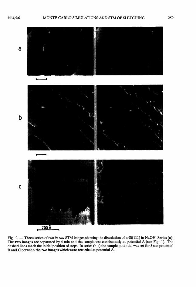
Figure 2 presents three series of two STM images [4-5] showing how Si etching proceeds atpotentials marked as A, B and C in figure 1. In series (a) the large density of electrons at the sur-face almost stops the dissolution. The series evidences however some etching which is completely
259
Fig. 2. - Three series of two in-situ STM images showing the dissolution of n-Si(lll) in NaOH. Series (a):The two images are separated by 4 min and the sample was continuously at potential A (see Fig. 1). Thedashed lines mark the initial position of steps. In series (b-c) the sample potential was set for 3 s at potentialB and C between the two images which were recorded at potential A.

260
anisotropic since it exclusively occurs at step edges (all steps are one bi-layer high, i.e. 3.1 Â high)and no pit formation is observed on terraces during the 4 minutes of observation. The initial posi-tion of step edges is shown by the dashed line in the second image of series (a). Between the twoimages in series (b) the Si has been set for only 3 s at potential B, which nearly corresponds to theusual situation in technology when the wafer is simply dipped in the etch bath. This procedure,also referred to as ’chemical etching’ results in pronounced pitting of terraces (all pits are 3.1 Adeep). In series (c) the sample has been also set at bias C, again for 3 s, between the two images.Faster pit formation is observed due to anodic polarization. Note also that pits are nearly circularcontrary to the triangular ones created in series (b).
Fig. 3. - Time sequence of in-situ STM images showing the growth of pits at potential A. The series startsfrom the second image of series (b) of figure 2. Images (b-d) were recorded 38, 114 and 152 s afterimage (a).
Imaging the very beginning of pit formation is practically impossible experimentally with n-Sisince long standing imaging is not possible in the corresponding electrochemical conditions [2, 4].

261
In figure 2b and c the pits have been nucleated during the potential pulse while the regulationloop for the tip current was simultaneously opened and the tip immobilized [4]. If one operatesat cathodic bias the event becomes so rare (see Fig. la) that imaging the initiation of nucleationis a matter of luck. Figure 3 studies the growth of etch pits immediately after their creation. Thisseries will be used for simulation. It evidences that the triangular shape is preserved over a longperiod until pit coalesce or merge into step edges.
3. Quantitative determinations from STM images.
Several parameters accounting for micro- and macroscopic phenomenon can be measured fromtime sequences of STM images. The determination of the bias dependence of some of theseparameters has yielded new insights into the dissolution mechanism of Si in NaOH [7]. The readeris referred to references [4, 5] for more details.The first parameter of interest in technology is the vertical etch rates Rn. Its expression is
given by (A5’/5’) - hot, where OS is the surface area of terraces which has disappeared, includ-ing eventual pits, in the time interval At, h is the step height and S the total surface area underobservation [the quantity (0394S/S)·h represents the volume of material removed per cm2 of sam-ple since the process is a layer by layer dissolution]. Macroscopically Rn is generally derived fromlosses of material and the result is averaged over several mm2 of sample. Although derived fromca 1000 x 1000 Â2 STM images the values of Rn are surprisingly very consistent with macroscopicdeterminations [4], with the advantage that etch rates as small as 0.2 Â/min can be determinedhere while they are very difficult to measure accurately with macroscopic methods. The lateraletch rate Ri is a second parameter of interest to characterize the reaction anisotropy. It is simplythe speed at which step migrate. This is a typical microscopic parameter that can not be reachedby other methods.
The anisotropy of the reaction can be defined as the ratio Rl/Rn. The larger this ratio themore anisotropic the etching. A macroscopic approach of the anisotropy is possible from etch ratemeasurements with samples of different orientations [6]. The frequency of etch pit generation isthe last parameter which is directly attainable from STM images. This is a microscopic parametersince pits seen with other techniques are much deeper and larger due to the coalescence of smallerones.
4. Détermination of the atomic reaction rates.
The alterations that the 3-D ideal surface structure of a Si(lll) surface (Fig. 4) undergoes withthe applied potential (see Fig. 2) reflect changes in the (electro-)chemical reactivity of the dif-ferent Si hydride species (mono-, di-, tri-hydrides), mostly in connection with variations of thesurface density of electrons. It is indeed well known that the surface of Si remains completely H-terminated, at all bias, as it has been explained by reaction models [7-9] and verified by ex-situ [10]as well as in-situ IR spectroscopy [11-12]. The purpose of this section is to show that the reactionrate on the different atomic sites at the surface are quantitatively attainable from the comparisonof simulations with the above experiments.
Chemically, the dissolution proceeds by the hydrolysis of Si-H bonds into a Si-OH group asinitial step. This polarizes the adjacent Si-Si back bonds and makes them unstable, which explainsthat Si-OH groups are removed from the surface [7-9]. The rate of dissolution depends on severalfactors including the accessibility of Si-H bonds to water molecules and the possibility to breakthe Si-Si back bonds. The strength of Si-H bonds and its angle with the surface are important for

262
Fig. 4. - 3-D view of the Si(111) surface. Each Si surface atom (open circles) is bound to one or several Hatoms (black circle) according to its coordination with the lattice. The kink site is grey shaded.
the hydrolysis step while steric hindrance governs the Si-Si bond breaking. Both factors explainsthat etching is favored at steps, especially when the reaction is chemical [7-9].
Physically, simulation (see Appendix) is based on the following assumptions. Silicon atomsare randomly removed from the surface at a rate ki (expressed in s-1 ) according to their latticecoordination. To simplify computation, we in fact consider three types of hexagonal sites centredon topmost atoms as shown in figure Al. Terrace sites (labelled as site T, reaction rate kT) whichinclude only one vertical monohydride - Si-H. Sites at step edges are of two kinds. The first ones(site S, rate ks) correspond to an hexagonal cell with one vertical - Si-H and, on average, one"horizontal" step edge monohydride - Si-H. The second type of step edge sites include eithera vertical or an horizontal Si dihydride group = Si-H2; They are considered as being equivalentin computations (site U, rate ku). Given these definitions and the mechanism of etching thedissolution rates k’s are expected to be in the series lot ks ku. Computed images correspondto 576 x 576 Â2 which is about one fourth of STM images (Fig. 2).
Figure 5 is a simulated time sequence showing the attack of a (111) terrace initially virgin of anydefect. The reaction rates are lot = 10-4 s-1, ks = 10-2 s-1 and ku = 1 s-1. The attack proceedswith the nucleation and growth of triangular pits which evidences the three possible orientations,parallel to the [110] directions, of stable - Si-H terminated step. The visual analogy between

263
Fig. Al. - Top view of the Si(111) surface defining the different atomic sites concerned in simulations.Each of them is an hexagon marked by a letter T, S and U, respectively for vertical terrace - SiH, step - SiHand step = SiH2 silicon hydride species.
simulations and STM images of figure 3 qualitatively validates the model. Figure 6 concems thedissolution at step edges. No pitting was allowed on terraces (lot = 0) to compare results with thesequence in figure 2a. The simulation was started after a row of sites, parallel to the [110], has beenartificially removed so as to initiate the attack at a - Si-H terminated step and at an unstable = Si-H2 terminated one, respectively exclusively composed of S sites on the right and of U sites on theleft side of arrows. In accordance with expectations the = SiH2 terminated step becomes rapidlyrougher and migrates faster than the =- Si-H terminated one which remains almost straight. Notethat a straight portion, corresponding to a - Si-H terminated step, is slowly appearing on the leftstep. Parameters were ks = 10-2 S-1 and ku = 1 s-1 as in figure 5.
5. Discussion.
5.1 COMPARISON WITH EXPERIMENT. - Figure 7 shows the time dependence of the etch ratefor different simulations. In the case of the attack at steps (Fig. 6) the etch rate was calculatedas exposed in section 2 with the surface under observation being the surface of the entire cell.The dissolution proceeds at a constant rate. That the ratio of speeds Ri with which the two typesof steps are migrating is only ,: 5 although the ratio kulks was set to 100 demonstrates that kinksites are governing the dissolution on "stable steps". With increasing probability ks the stable stepmove faster and becomes rougher.
In the case of the growth of pits, such as in the STM experiment of figure 3, the etch rate wascalculated by subtracting the image obtained at time t with the initial one. In the case of figure 3the first image was taken as reference. To compare experimental data with simulations the originof computed times was taken such that the size of simulated pits would make them easily visiblein STM images [e.g. t = 59 s was taken as origin of times in the case of Fig. 5].
Figure 7 evidences an exponential time dependence of the initial growth of pit, both in sim-

264
Fig. 5. - Simulated time sequence of images showing the nucleation and growth of pits on a virgin terrace.Parameters are azur = 10-4 s-1, ks = 10-2 s-1 and ku = 1 s-1.
ulations (curves a and b) and experimentally z) which further justifies our model. A relativeagreement with STM data is obtained with 5 x 10⁻⁵ kit 10-4 s-1, ks = 10-2 s-1 and leu = 1s-1. The uncertainty in the determination of lot stems from the fact that the etch rate derived fromSTM images includes the attack at steps in contrast to simulations where pits are solely consid-ered. The number of Si layers exposed to solution being about 4 - 5 on average in 1400 x 1400 A2STM images (Fig. 2) and simulated images being one fourth of STM images, experimental datacan be better accounted for by adding the etch rate at one step to the growth of pits, as in figure5. This is demonstrated by curve (+) in figure 7 which is the sum of curve (b) and the average (0.3Â/min) of etch rates at "= SiH2 " and "= SiH" steps (see above curves c and d of Fig. 7).The applied potential has a drastic effect of the dissolution rates. For instance, simulating the
time sequence shown in figure 2c, requires lot = 0.01 s-1, leu - 1 s-1 and ks = 0.5 s-1, whichillustrates the activation by potential of the electrochemical reaction on the most stable atoms(the rate kit is multiplied by a factor 5 x 10³ and ku by 50).
5.2 INTERPRETATION OF SIMULATION. - Given the quantitative agreement between simula-tions and STM images it can be concluded that Si etching actually occurs according to the ran-dom removal of atoms from the surface. No surface diffusion needs being considered, which isconsistent with the covalent nature of Si.
It is very interesting to notice in simulated images that isolated missing terrace sites do notnecessarily lead to immediate growth of a pit. Such "point defects" look stable upon long periodsof time. The rate of pit growth really increases if 2 - 3 other terrace sites are attacked next to

265
Fig. 6. - Simulated time sequence of images showing the attack at two steps. The one on the left is = SiH2terminated (unstable step) and that on the right is =- SiH terminated (stable step). Arrows give the positionof the row of atoms removed before experiment. Parameters are ks = 10-2 s-1 and ku = 1 s-1 and kT = 0s-1 (no pitting allowed).
the first one. This result fits very well reality if one considers that the "attack" of the very firstterrace site corresponds actually to the hydrolysis step of the vertical - Si-H monohydride, thesubsequent attack on neighbouring sites corresponding also to Si-OH formation followed by rapidremoval of the 2 - 3 terrace - Si-OH. That several neighbouring - Si-OH groups are necessary toinitiate a pit agrees with the picture that the process requires to overcome a great energy barrierto break the Si-Si back bonds underneath a - Si-OH group. Large strains are expected whencomparing the hard sphere diameter of a water molecule (2.9 Â) and the Si-Si bond length (2.35Â). The surface needs being made unstable by strong polarization of the Si-Si back bonds [7].This observation is supported by the fact that Si-OH bonds (which are precursor to dissolution)have been recently identified by in-situ STM after the surface was held at the rest potential for ashort period of time [13].
6. Conclusion.
In summary, we have presented a quantitative analysis of time sequences of in-situ STM imagesshowing Si etching with the resolution of atomic steps. The comparison of experiments withMonte-Carlo simulation demonstrates that the dissolution of Si proceeds according to the randomremoval of Si atoms from the surface. Reaction rates on the atomic scale have been determined

266
Fig. 7. - Simulated and experimental time dependence of the etch rate. Experimental () data are derivedfrom figure 3. Curve (a) corresponds to figure 5 (kT = 10-4 s-l) and curve (b) is calculated with kT = 510-5s-1 (ks = 10-2 s-1 and ku = 1 s-1 in both cases). Curves (c) and (d) correspond to the attack at - SiHand = SiH2 terminated steps (kT = 0 s-l, ks = 10-2 s-1 and ku = 1 s-1 ). Curve (+) is the sum of curve(b) with the average of etch rates at steps.
for the first time with this method. Results evidence that the reaction rate on kink sites is mostlygoverning the macroscopic speed of the reaction and that the bias has a drastic effect on othersites.
Appendix
Physically, at time t, the surface consists in ni (t) atoms of type i whose rate of dissolution (con-stant ki, expressed in s-1 ) is only depending on their lattice coordination. The total dissolutionrate of the surface being therefore simply given by the sum 03A3(i)kini(t), one atom is removed, onaverage, during the time interval dt = 1/(03A3(i)kini(t)).
Simulation consist in the successive random removal of hexagonal sites Si atomic sites shownin figure Al. To simplify three types of sites are considered. The time increment in simulationis taken as At = 1/(03A3(i = T, S, U)kini(t)) (At is not constant since the populations ni varywith time) and we consider that exactly one atom is removed from the surface during Ot (thisavoids unsuccessful attempts). Statistics concerns however which atom is removed. This is doneat random in two stages.The type of the site is first defined by establishing the three populations ni (t) and ratio vi
kini(t)/(L:(j = T, S, U)kjnj(t)) which represent the probability ( 0 vi 1) to remove a siteof type i between t and t + At. Physically vi represents the (normalized) partial speeds of thereaction on all sites of type i. Choosing at random a number x (0 x 1), designs the family j if03A3(i j ) (v2 ) x 03A3(i~j)(vi). After this stage, the atomic site which is actually attacked isthen chosen, also at random among a list of the nj (t) sites of type j (they are all equiprobable).Given the foregoing definitions, it is important to notice that the kas may be greater than unity.
267
References
[1] Siegenthaler H., in "Scanning Tunneling Microscopy II", R. Wiesendanger and H.-J. Güntherodt Eds.,Springer Series Surf. Sci. 28 (1992).
[2] Allongue P., in "Advances in Electrochemical Science and Engineering", H. Gerischer and C. W. TobiasEds., Vol. 4, Weinheim, in press.
[3] Morrison S.R., in "Electrochemistry at Semiconductor and Oxidized Metal Electrodes" (Plenum Press,New York, 1980).
[4] Allongue P., Kieling V and Gerischer H., J. Electrochem. Soc. 140 (1993) 1009.[5] Allongue P., Brune H. and Gerischer H., Surf. Sci. 275 (1992) 414.[6] Kendall D.L., Ann. Rev. Mater Sci. 9 (1979) 373 and Seidel H., Csepregi L., Heuberger A. and
Baumgärtel H., J. Electrochem. Soc. 137 (1990) 3612 and 3626.[7] Allongue P., Kieling V and Gerischer H., J. Electrochem. Soc. 140 (1993) 1018.[8] Gerischer H., Allongue P. and Costa-Kieling V., Ber. Bunsenges. Phys. Chem. 97 (1993) 753.[9] Allongue P., Kieling V and Gerischer H., Electrochim. Acta, in press.
[10] For a review, see Higashi G.S. and Chabal Y.J., in "Handbook of Semiconductor Wafer CleaningTechnology", W. Kern Ed. (Noyes Publications, Park Ridge, 1993).
[11] Venkateswara Rao A., Ozanam F. and Chazalviel J.-N., J. Electrochem. Soc. 138 (1991) 153.[12] Rappich J., Lewerenz H.J. and Gerischer H., J. Electrochem. Soc. 141 (1994) L187.[13] Allongue P., to be published.