wet etching · 2017-10-03 · r. b. darling / ee-527 / winter 2013 outline • general features of...
TRANSCRIPT
R. B. Darling / EE-527 / Winter 2013
EE-527: MicroFabrication
Wet Etching
R. B. Darling / EE-527 / Winter 2013
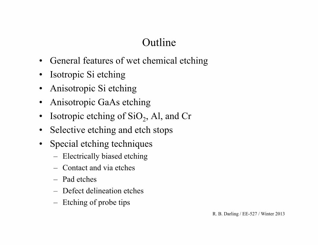
Outline• General features of wet chemical etching• Isotropic Si etching• Anisotropic Si etching• Anisotropic GaAs etching• Isotropic etching of SiO2, Al, and Cr• Selective etching and etch stops• Special etching techniques
– Electrically biased etching– Contact and via etches– Pad etches– Defect delineation etches– Etching of probe tips
R. B. Darling / EE-527 / Winter 2013
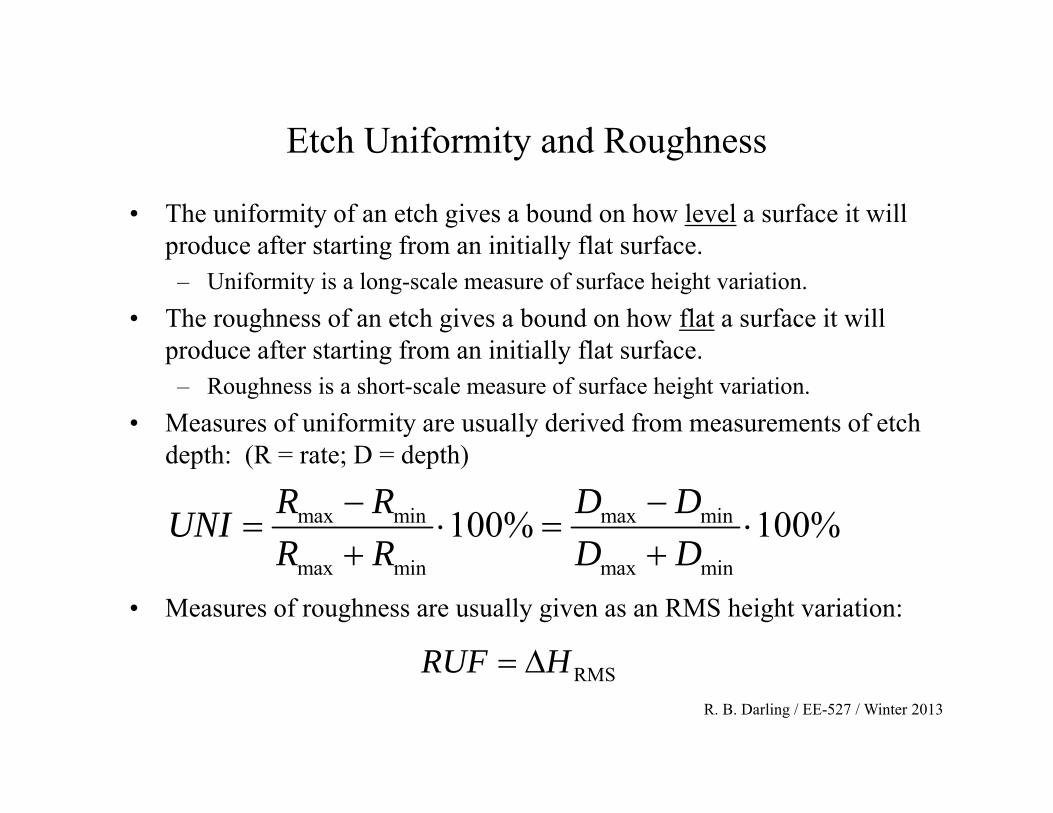
Etch Uniformity and Roughness
• The uniformity of an etch gives a bound on how level a surface it will produce after starting from an initially flat surface. – Uniformity is a long-scale measure of surface height variation.
• The roughness of an etch gives a bound on how flat a surface it will produce after starting from an initially flat surface. – Roughness is a short-scale measure of surface height variation.
• Measures of uniformity are usually derived from measurements of etch depth: (R = rate; D = depth)
• Measures of roughness are usually given as an RMS height variation:
max min max min
max min max min
100% 100%R R D DUNIR R D D
RMSHRUF
R. B. Darling / EE-527 / Winter 2013
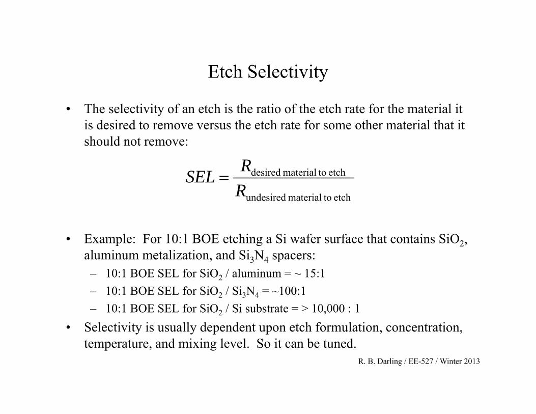
Etch Selectivity
• The selectivity of an etch is the ratio of the etch rate for the material it is desired to remove versus the etch rate for some other material that it should not remove:
• Example: For 10:1 BOE etching a Si wafer surface that contains SiO2, aluminum metalization, and Si3N4 spacers:
– 10:1 BOE SEL for SiO2 / aluminum = ~ 15:1– 10:1 BOE SEL for SiO2 / Si3N4 = ~100:1– 10:1 BOE SEL for SiO2 / Si substrate = > 10,000 : 1
• Selectivity is usually dependent upon etch formulation, concentration, temperature, and mixing level. So it can be tuned.
etch tomaterial undesired
etch tomaterial desired
RRSEL
R. B. Darling / EE-527 / Winter 2013
Etch Anisotropy
• Isotropic etching– Same etch rate in all directions– Lateral etch rate is about the same as vertical etch rate– Etch rate does not depend upon the orientation of the mask edge
• Anisotropic etching– Etch rate depends upon orientation to crystalline planes– Lateral etch rate can be much larger or smaller than vertical etch
rate, depending upon orientation of mask edge to crystalline axes– Orientation of mask edge and the details of the mask pattern
determine the final etched shape• Can be very useful for making complex shapes• Can be very surprising if not carefully thought out• Only certain “standard” shapes are routinely used
R. B. Darling / EE-527 / Winter 2013
Etching Chemistry
• The etching process involves: – Transport of reactants to the surface– Surface reaction– Transport of products from the surface
• Key ingredients in any wet etchant: – Oxidizer
• examples: H2O2, HNO3
– Acid or base to dissolve the oxidized surface• examples: H2SO4, NH4OH
– Dilutent media to transport reactants and products through• examples: H2O, CH3COOH
R. B. Darling / EE-527 / Winter 2013
Redox Reactions
• Etching is inherently an electrochemical process: – It involves electron transfer processes as part of the surface
reactions.
• The oxidation number is the net positive charge on a species.
• Oxidation is the process of electron loss, or increase in the oxidation number.
• Reduction is the process of electron gain, or decrease in the oxidation number.
• Redox reactions are those composed of oxidation of one or more species and simultaneous reduction of others.
R. B. Darling / EE-527 / Winter 2013
HNA Etching of Silicon - 1
• Hydrofluoric acid + Nitric acid + Acetic acid• Produces nearly isotropic etching of Si• Overall reaction is:
– Si + HNO3 + 6HF H2SiF6 + HNO2 + H2O + H2
– Etching occurs via a redox reaction followed by dissolution of the oxide by an acid (HF) that acts as a complexing agent.
– Points on the Si surface randomly become oxidation or reduction sites. These act like localized electrochemical cells, sustaining corrosion currents of ~100 A/cm2 (relatively large).
– Each point on the surface becomes both an anode and cathode site over time. If the time spent on each is the same, the etching will be uniform; otherwise selective etching will occur.
R. B. Darling / EE-527 / Winter 2013
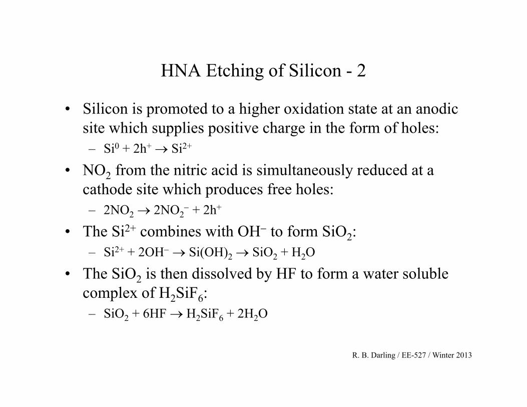
HNA Etching of Silicon - 2
• Silicon is promoted to a higher oxidation state at an anodic site which supplies positive charge in the form of holes: – Si0 + 2h+ Si2+
• NO2 from the nitric acid is simultaneously reduced at a cathode site which produces free holes: – 2NO2 2NO2
+ 2h+
• The Si2+ combines with OH to form SiO2: – Si2+ + 2OH Si(OH)2 SiO2 + H2O
• The SiO2 is then dissolved by HF to form a water soluble complex of H2SiF6: – SiO2 + 6HF H2SiF6 + 2H2O
R. B. Darling / EE-527 / Winter 2013
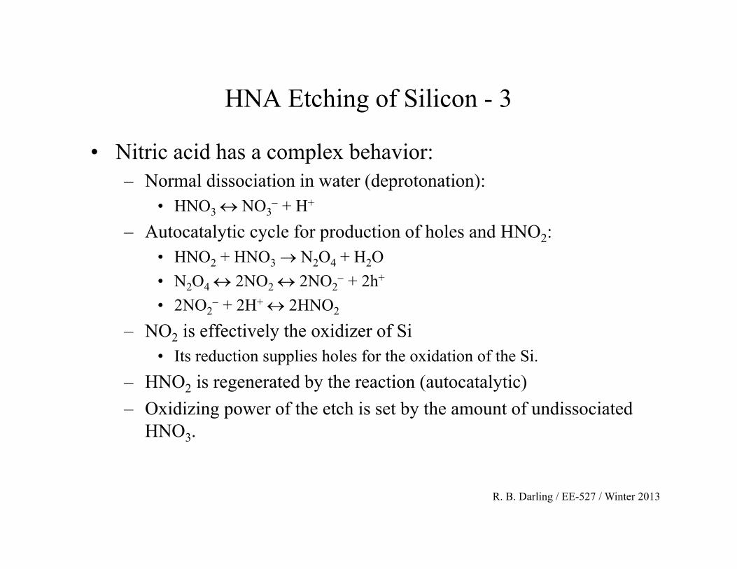
HNA Etching of Silicon - 3
• Nitric acid has a complex behavior: – Normal dissociation in water (deprotonation):
• HNO3 NO3 + H+
– Autocatalytic cycle for production of holes and HNO2: • HNO2 + HNO3 N2O4 + H2O• N2O4 2NO2 2NO2
+ 2h+
• 2NO2 + 2H+ 2HNO2
– NO2 is effectively the oxidizer of Si• Its reduction supplies holes for the oxidation of the Si.
– HNO2 is regenerated by the reaction (autocatalytic)– Oxidizing power of the etch is set by the amount of undissociated
HNO3.
R. B. Darling / EE-527 / Winter 2013
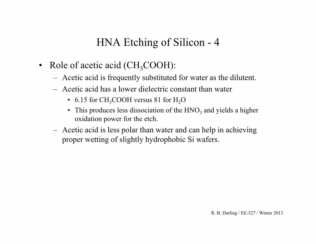
HNA Etching of Silicon - 4
• Role of acetic acid (CH3COOH): – Acetic acid is frequently substituted for water as the dilutent. – Acetic acid has a lower dielectric constant than water
• 6.15 for CH3COOH versus 81 for H2O• This produces less dissociation of the HNO3 and yields a higher
oxidation power for the etch. – Acetic acid is less polar than water and can help in achieving
proper wetting of slightly hydrophobic Si wafers.
R. B. Darling / EE-527 / Winter 2013
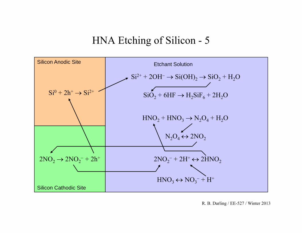
HNA Etching of Silicon - 5
Silicon Anodic Site
Silicon Cathodic Site
Etchant Solution
Si0 + 2h+ Si2+
2NO2 2NO2 + 2h+
Si2+ + 2OH Si(OH)2 SiO2 + H2O
SiO2 + 6HF H2SiF6 + 2H2O
HNO3 NO3 + H+
HNO2 + HNO3 N2O4 + H2O
2NO2 + 2H+ 2HNO2
N2O4 2NO2
R. B. Darling / EE-527 / Winter 2013
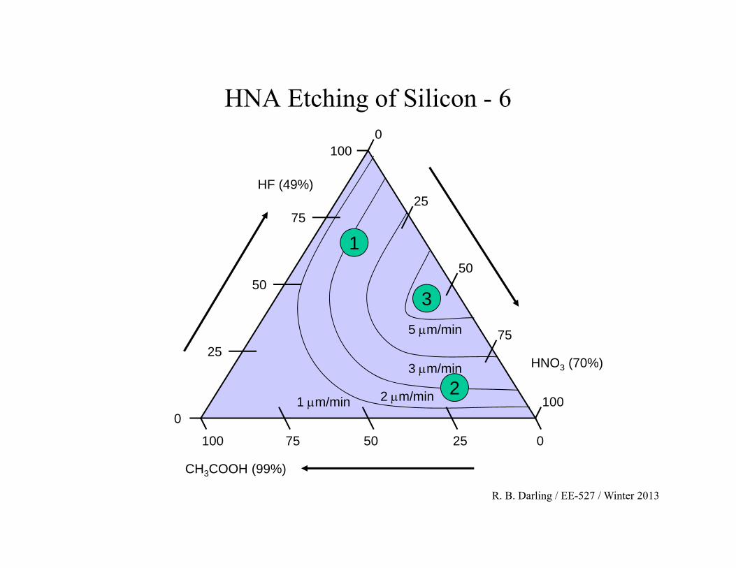
HNA Etching of Silicon - 6
HF (49%)
CH3COOH (99%)
HNO3 (70%)
75 50 25 0100
0
25
50
75
1000
25
50
75
100
5 m/min
3 m/min
2 m/min1 m/min
1
3
2
R. B. Darling / EE-527 / Winter 2013
HNA Etching of Silicon - 7
• Region– For high HF concentrations, contours are parallel to the lines of
constant HNO3; therefore the etch rate is controlled by HNO3 in this region.
– Leaves little residual oxide; limited by oxidation process.
• Region– For high HNO3 concentrations, contours are parallel to the lines of
constant HF; therefore the etch rate is controlled by HF in this region.
– Leaves a residual 30-50 Angstroms of SiO2; self-passivating; limited by oxide dissolution; area for polishing.
• Region– Initially not very sensitive to the amount of H2O, then etch rate
falls of sharply for 1:1 HF:HNO3 ratios.
1
2
3
R. B. Darling / EE-527 / Winter 2013
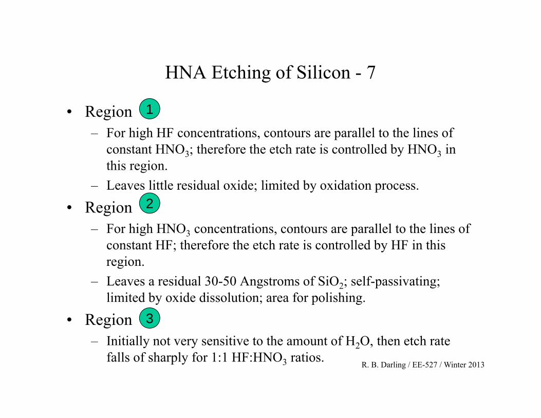
Isoetch Contours
HF (49%)
CH3COOH (99%)
HNO3 (70%)
75 50 25 0100
0
25
50
75
1000
25
50
75
100
5 m/min
3 m/min
2 m/min1 m/min
30
20
EXAMPLE:HF:HNO3:CH3COOH3:2:5 ratio by volume
R. B. Darling / EE-527 / Winter 2013
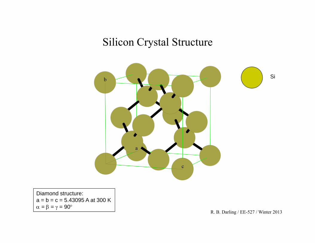
Silicon Crystal Structure
a
b
c
Diamond structure: a = b = c = 5.43095 A at 300 K = = = 90
Si

R. B. Darling / EE-527 / Winter 2013
Anisotropic Etching of Silicon - 1
• Differing hybridized (sp3) orbital orientation on different crystal planes causes drastic differences in etch rate.
• Typically, etch rates are: (110) > (100) >>> (111). • The (111) family of crystallographic planes are normally
the “stop” planes for anisotropic etching. • There are 8 (111) planes along the ± x ± y ± z unit vectors. • Intersections of these planes with planar bottoms produce
the standard anisotropic etching structures for (100) Si wafers:– V-grooves– pyramidal pits– pyramidal cavities
R. B. Darling / EE-527 / Winter 2013
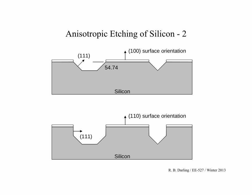
Anisotropic Etching of Silicon - 2
(110) surface orientation
(111)
(100) surface orientation(111)
54.74
Silicon
Silicon
R. B. Darling / EE-527 / Winter 2013
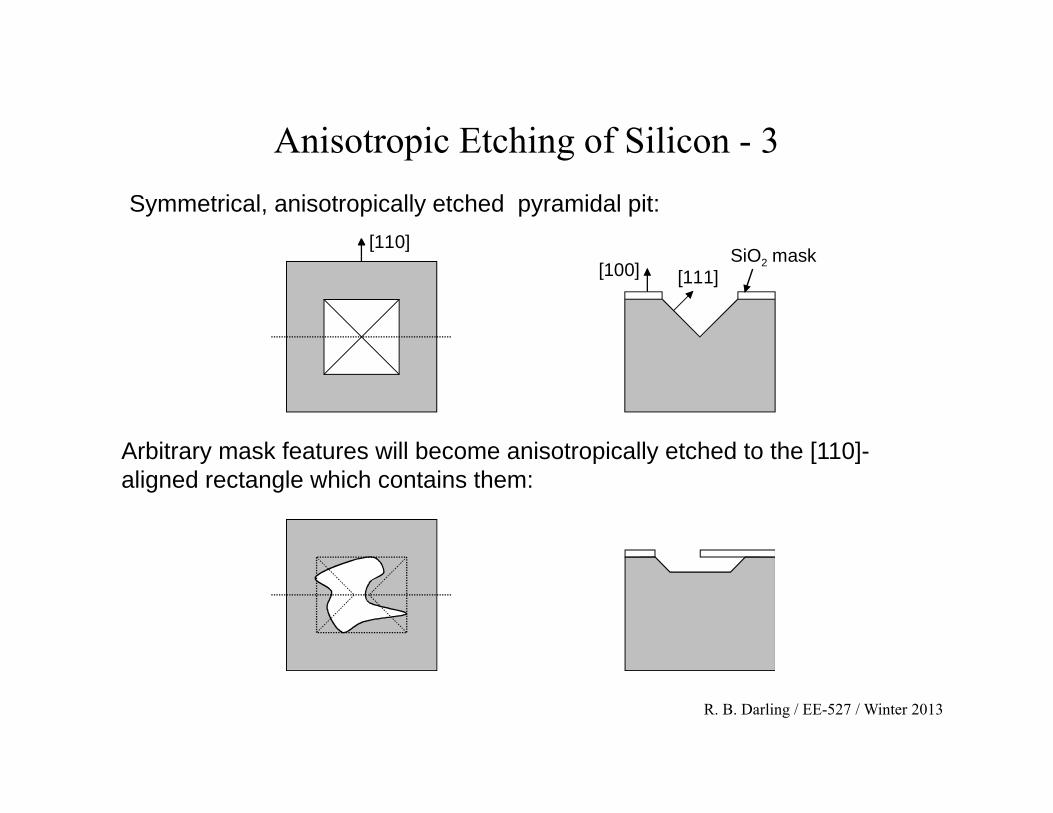
Anisotropic Etching of Silicon - 3
[110][100] [111]
SiO2 mask
Symmetrical, anisotropically etched pyramidal pit:
Arbitrary mask features will become anisotropically etched to the [110]-aligned rectangle which contains them:
R. B. Darling / EE-527 / Winter 2013
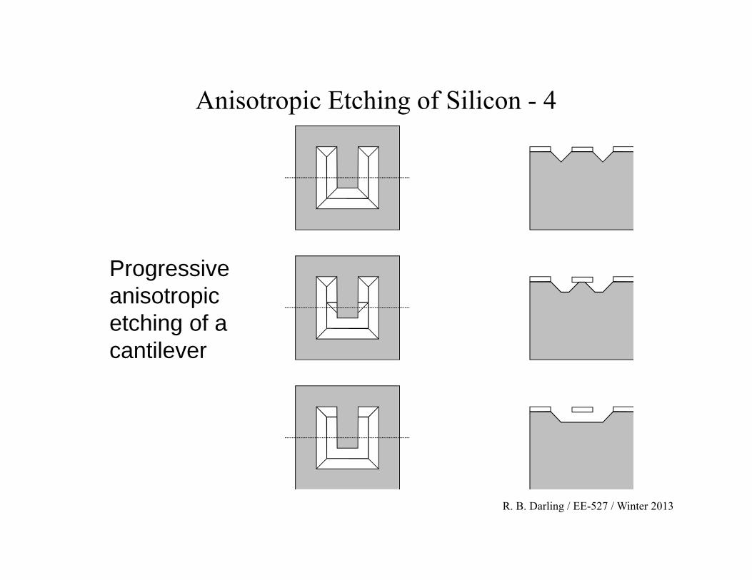
Anisotropic Etching of Silicon - 4
Progressive anisotropic etching of a cantilever
R. B. Darling / EE-527 / Winter 2013
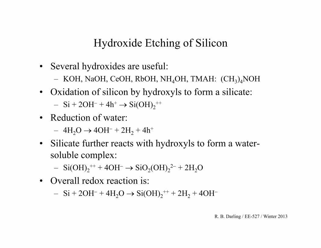
Hydroxide Etching of Silicon
• Several hydroxides are useful: – KOH, NaOH, CeOH, RbOH, NH4OH, TMAH: (CH3)4NOH
• Oxidation of silicon by hydroxyls to form a silicate: – Si + 2OH + 4h+ Si(OH)2
++
• Reduction of water: – 4H2O 4OH + 2H2 + 4h+
• Silicate further reacts with hydroxyls to form a water-soluble complex: – Si(OH)2
++ + 4OH SiO2(OH)22 + 2H2O
• Overall redox reaction is: – Si + 2OH + 4H2O Si(OH)2
++ + 2H2 + 4OH
R. B. Darling / EE-527 / Winter 2013
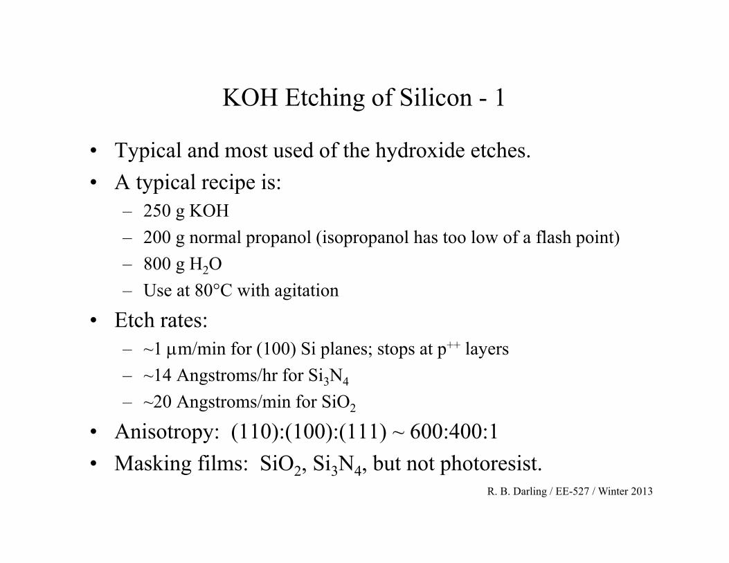
KOH Etching of Silicon - 1
• Typical and most used of the hydroxide etches. • A typical recipe is:
– 250 g KOH– 200 g normal propanol (isopropanol has too low of a flash point)– 800 g H2O– Use at 80°C with agitation
• Etch rates: – ~1 m/min for (100) Si planes; stops at p++ layers– ~14 Angstroms/hr for Si3N4
– ~20 Angstroms/min for SiO2
• Anisotropy: (110):(100):(111) ~ 600:400:1• Masking films: SiO2, Si3N4, but not photoresist.
R. B. Darling / EE-527 / Winter 2013
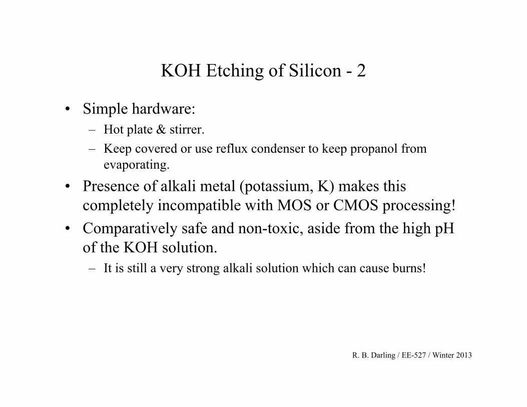
KOH Etching of Silicon - 2
• Simple hardware: – Hot plate & stirrer. – Keep covered or use reflux condenser to keep propanol from
evaporating.
• Presence of alkali metal (potassium, K) makes this completely incompatible with MOS or CMOS processing!
• Comparatively safe and non-toxic, aside from the high pH of the KOH solution. – It is still a very strong alkali solution which can cause burns!
R. B. Darling / EE-527 / Winter 2013
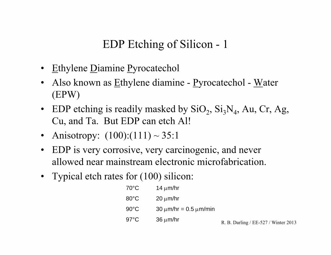
EDP Etching of Silicon - 1
• Ethylene Diamine Pyrocatechol• Also known as Ethylene diamine - Pyrocatechol - Water
(EPW)• EDP etching is readily masked by SiO2, Si3N4, Au, Cr, Ag,
Cu, and Ta. But EDP can etch Al! • Anisotropy: (100):(111) ~ 35:1• EDP is very corrosive, very carcinogenic, and never
allowed near mainstream electronic microfabrication. • Typical etch rates for (100) silicon:
70°C 14 m/hr
80°C 20 m/hr
90°C 30 m/hr = 0.5 m/min
97°C 36 m/hr
R. B. Darling / EE-527 / Winter 2013
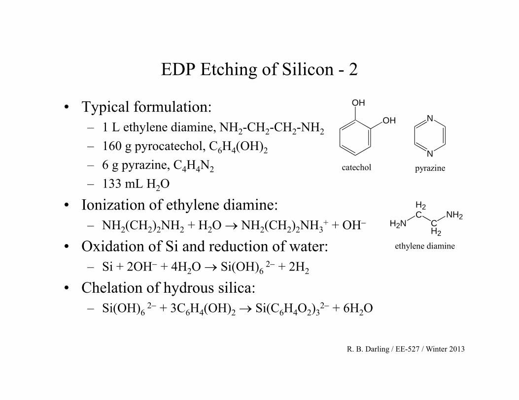
EDP Etching of Silicon - 2
• Typical formulation: – 1 L ethylene diamine, NH2-CH2-CH2-NH2
– 160 g pyrocatechol, C6H4(OH)2
– 6 g pyrazine, C4H4N2
– 133 mL H2O
• Ionization of ethylene diamine: – NH2(CH2)2NH2 + H2O NH2(CH2)2NH3
+ + OH
• Oxidation of Si and reduction of water: – Si + 2OH + 4H2O Si(OH)6
2 + 2H2
• Chelation of hydrous silica: – Si(OH)6
2 + 3C6H4(OH)2 Si(C6H4O2)32 + 6H2O
OH
OH
catechol
N
Npyrazine
H2N
H2C
CH2
NH2
ethylene diamine
R. B. Darling / EE-527 / Winter 2013
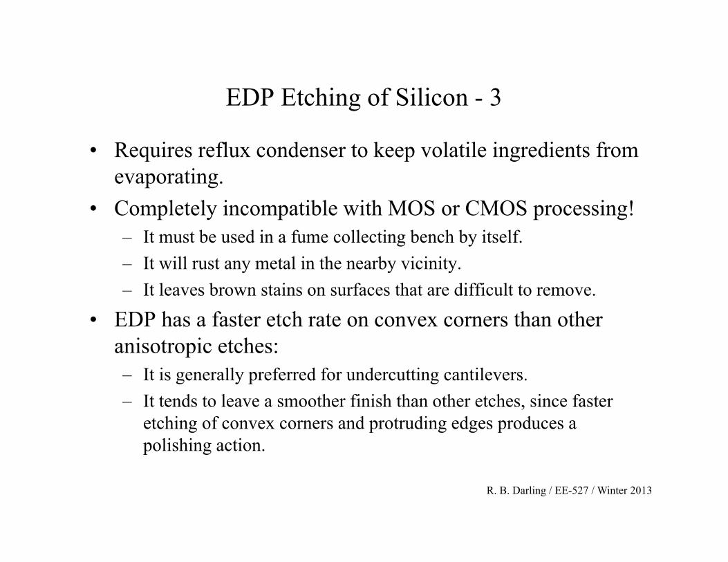
EDP Etching of Silicon - 3
• Requires reflux condenser to keep volatile ingredients from evaporating.
• Completely incompatible with MOS or CMOS processing! – It must be used in a fume collecting bench by itself. – It will rust any metal in the nearby vicinity. – It leaves brown stains on surfaces that are difficult to remove.
• EDP has a faster etch rate on convex corners than other anisotropic etches: – It is generally preferred for undercutting cantilevers. – It tends to leave a smoother finish than other etches, since faster
etching of convex corners and protruding edges produces a polishing action.
R. B. Darling / EE-527 / Winter 2013
EDP Etching of Silicon - 4
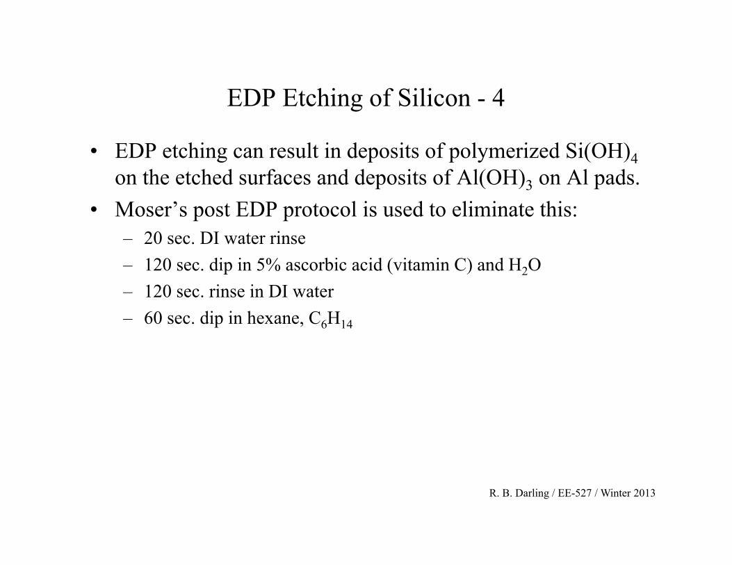
• EDP etching can result in deposits of polymerized Si(OH)4on the etched surfaces and deposits of Al(OH)3 on Al pads.
• Moser’s post EDP protocol is used to eliminate this: – 20 sec. DI water rinse– 120 sec. dip in 5% ascorbic acid (vitamin C) and H2O– 120 sec. rinse in DI water– 60 sec. dip in hexane, C6H14
R. B. Darling / EE-527 / Winter 2013
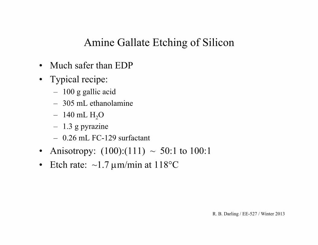
Amine Gallate Etching of Silicon
• Much safer than EDP• Typical recipe:
– 100 g gallic acid– 305 mL ethanolamine– 140 mL H2O– 1.3 g pyrazine– 0.26 mL FC-129 surfactant
• Anisotropy: (100):(111) ~ 50:1 to 100:1• Etch rate: ~1.7 m/min at 118°C
R. B. Darling / EE-527 / Winter 2013
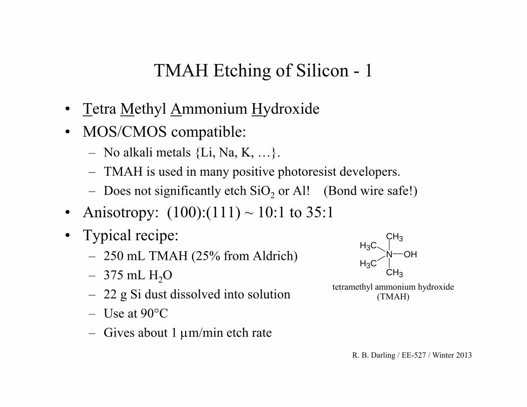
TMAH Etching of Silicon - 1
• Tetra Methyl Ammonium Hydroxide• MOS/CMOS compatible:
– No alkali metals {Li, Na, K, …}. – TMAH is used in many positive photoresist developers.– Does not significantly etch SiO2 or Al! (Bond wire safe!)
• Anisotropy: (100):(111) ~ 10:1 to 35:1• Typical recipe:
– 250 mL TMAH (25% from Aldrich)– 375 mL H2O– 22 g Si dust dissolved into solution– Use at 90°C– Gives about 1 m/min etch rate
CH3
N
CH3
H3C
H3COH
tetramethyl ammonium hydroxide(TMAH)
R. B. Darling / EE-527 / Winter 2013
TMAH Etching of Silicon - 2• Hydroxide etches are generally safe and predictable, but
they usually involve an alkali metal which makes them incompatible with MOS or CMOS processing.
• Ammonium hydroxide (NH4OH) is one hydroxide which is free of alkali metal, but it is really ammonia which is dissolved into water. Heating to 90°C for etching will rapidly evaporate the ammonia from solution.
• Ballasting the ammonium hydroxide with a less volatile organic solves the problem: – Tetramethyl ammonium hydroxide: (CH3)4NOH (TMAH)– Tetraethyl ammonium hydroxide: (C2H5)4NOH (TEAH)
• TMAH has recently been found to be more toxic than previously thought – it appears to be a neurotoxin.
R. B. Darling / EE-527 / Winter 2013
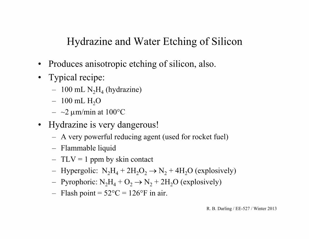
Hydrazine and Water Etching of Silicon
• Produces anisotropic etching of silicon, also. • Typical recipe:
– 100 mL N2H4 (hydrazine)– 100 mL H2O– ~2 m/min at 100°C
• Hydrazine is very dangerous!– A very powerful reducing agent (used for rocket fuel)– Flammable liquid– TLV = 1 ppm by skin contact– Hypergolic: N2H4 + 2H2O2 N2 + 4H2O (explosively)– Pyrophoric: N2H4 + O2 N2 + 2H2O (explosively)– Flash point = 52°C = 126°F in air.
R. B. Darling / EE-527 / Winter 2013
Anisotropic Etch Stop Layers - 1
• Controlling the absolute depth of an etch is often difficult, particularly if the etch is going most of the way through a wafer.
• Etch stop layers can be used to drastically slow the etch rate, providing a stopping point of high absolute accuracy.
• Boron doping is most commonly used for silicon etching. • Requirements for specific etches:
– HNA etch actually speeds up for heavier doping– KOH etch rate reduces by 20 for boron doping > 1020 cm-3
– NaOH etch rate reduces by 10 for boron doping > 3 1020 cm-3
– EDP etch rate reduces by 50 for boron doping > 7 1019 cm-3
– TMAH etch rate reduces by 10 for boron doping > 1020 cm-3
R. B. Darling / EE-527 / Winter 2013
Anisotropic Etch Stop Layers - 2
2-5 m thick membrane
400 - 500 mthick wafer
heavily boron doped etch stop layer
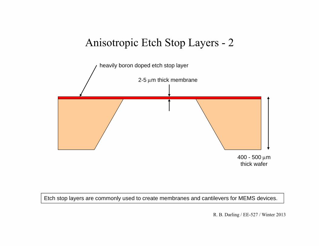
Etch stop layers are commonly used to create membranes and cantilevers for MEMS devices.
R. B. Darling / EE-527 / Winter 2013
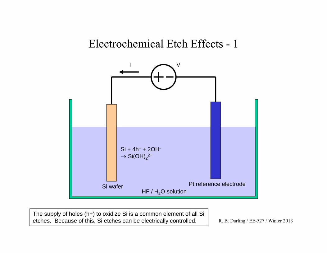
Electrochemical Etch Effects - 1
Si wafer Pt reference electrodeHF / H2O solution
Si + 4h+ + 2OH-
Si(OH)22+
VI
The supply of holes (h+) to oxidize Si is a common element of all Si etches. Because of this, Si etches can be electrically controlled.
R. B. Darling / EE-527 / Winter 2013
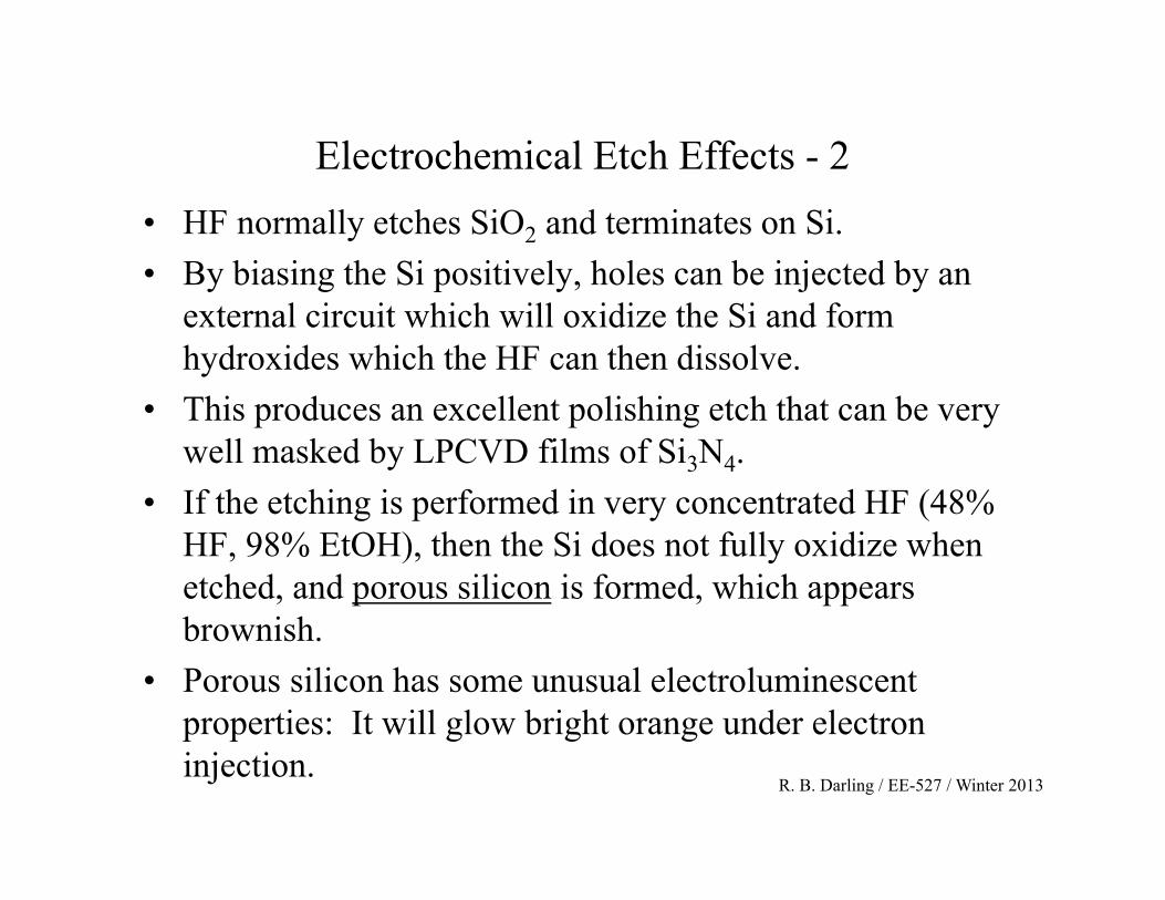
Electrochemical Etch Effects - 2• HF normally etches SiO2 and terminates on Si. • By biasing the Si positively, holes can be injected by an
external circuit which will oxidize the Si and form hydroxides which the HF can then dissolve.
• This produces an excellent polishing etch that can be very well masked by LPCVD films of Si3N4.
• If the etching is performed in very concentrated HF (48% HF, 98% EtOH), then the Si does not fully oxidize when etched, and porous silicon is formed, which appears brownish.
• Porous silicon has some unusual electroluminescent properties: It will glow bright orange under electron injection.
R. B. Darling / EE-527 / Winter 2013
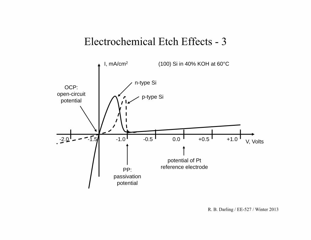
Electrochemical Etch Effects - 3
0.0-1.5 -1.0 -0.5 +0.5 +1.0-2.0
I, mA/cm2
V, Volts
(100) Si in 40% KOH at 60°C
potential of Ptreference electrodePP:
passivationpotential
n-type Si
p-type Si
OCP:open-circuit
potential
R. B. Darling / EE-527 / Winter 2013
Electrochemical Etch Effects - 4
• The open circuit potential (OCP) is the difference between the half-cell potentials of the Si wafer and the Pt electrode. – This is usually about −1.50 V, varying a bit with temperature and
solution concentration.
• Increasing the wafer bias above the OCP will increase the etch rate by supplying holes which will oxidize the Si.
• Increasing the wafer bias further will reach the passivation potential (PP) where SiO2 forms. – This passivates the surface and terminates the etch. The SiO2
creates an insulating film which drastically reduces the current flow.
– The HF / H2O solution does not exhibit a PP, since the SiO2 is constantly and rapidly dissolved by the HF.
R. B. Darling / EE-527 / Winter 2013
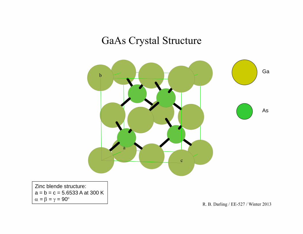
GaAs Crystal Structure
a
b
c
Zinc blende structure: a = b = c = 5.6533 A at 300 K = = = 90
Ga
As
R. B. Darling / EE-527 / Winter 2013
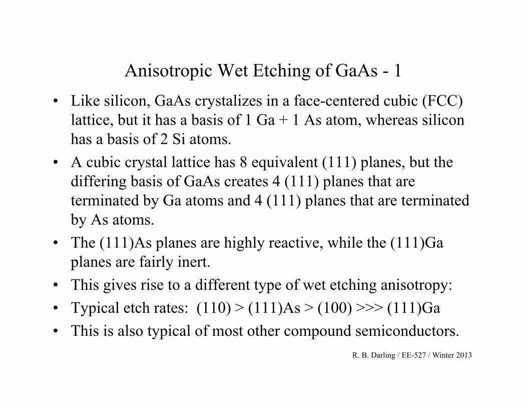
Anisotropic Wet Etching of GaAs - 1• Like silicon, GaAs crystalizes in a face-centered cubic (FCC)
lattice, but it has a basis of 1 Ga + 1 As atom, whereas silicon has a basis of 2 Si atoms.
• A cubic crystal lattice has 8 equivalent (111) planes, but the differing basis of GaAs creates 4 (111) planes that are terminated by Ga atoms and 4 (111) planes that are terminated by As atoms.
• The (111)As planes are highly reactive, while the (111)Ga planes are fairly inert.
• This gives rise to a different type of wet etching anisotropy: • Typical etch rates: (110) > (111)As > (100) >>> (111)Ga• This is also typical of most other compound semiconductors.
R. B. Darling / EE-527 / Winter 2013
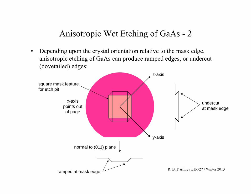
Anisotropic Wet Etching of GaAs - 2
• Depending upon the crystal orientation relative to the mask edge, anisotropic etching of GaAs can produce ramped edges, or undercut (dovetailed) edges:
y-axis
z-axis
x-axispoints outof page
normal to (011) plane
square mask featurefor etch pit
undercutat mask edge
ramped at mask edge
R. B. Darling / EE-527 / Winter 2013
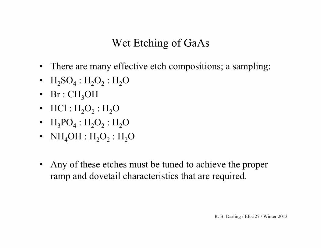
Wet Etching of GaAs
• There are many effective etch compositions; a sampling: • H2SO4 : H2O2 : H2O• Br : CH3OH• HCl : H2O2 : H2O• H3PO4 : H2O2 : H2O• NH4OH : H2O2 : H2O
• Any of these etches must be tuned to achieve the proper ramp and dovetail characteristics that are required.
R. B. Darling / EE-527 / Winter 2013
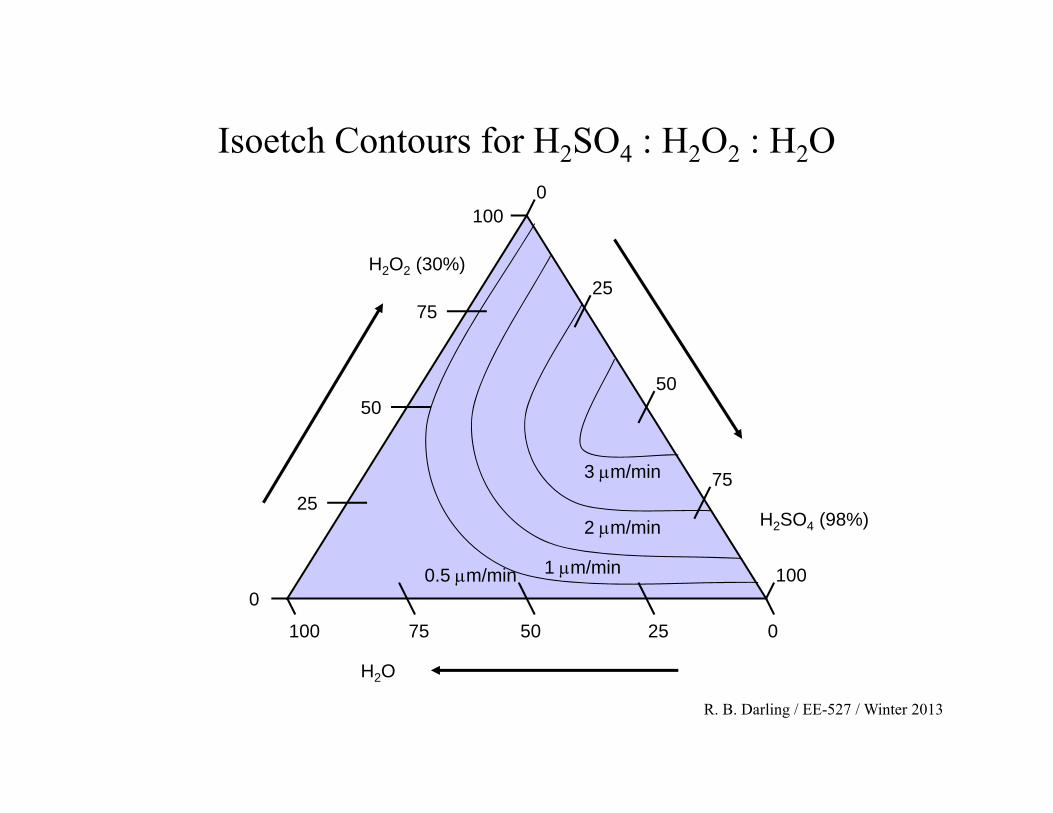
Isoetch Contours for H2SO4 : H2O2 : H2O
H2O2 (30%)
H2O
H2SO4 (98%)
75 50 25 0100
0
25
50
75
1000
25
50
75
100
3 m/min
2 m/min
1 m/min0.5 m/min
R. B. Darling / EE-527 / Winter 2013
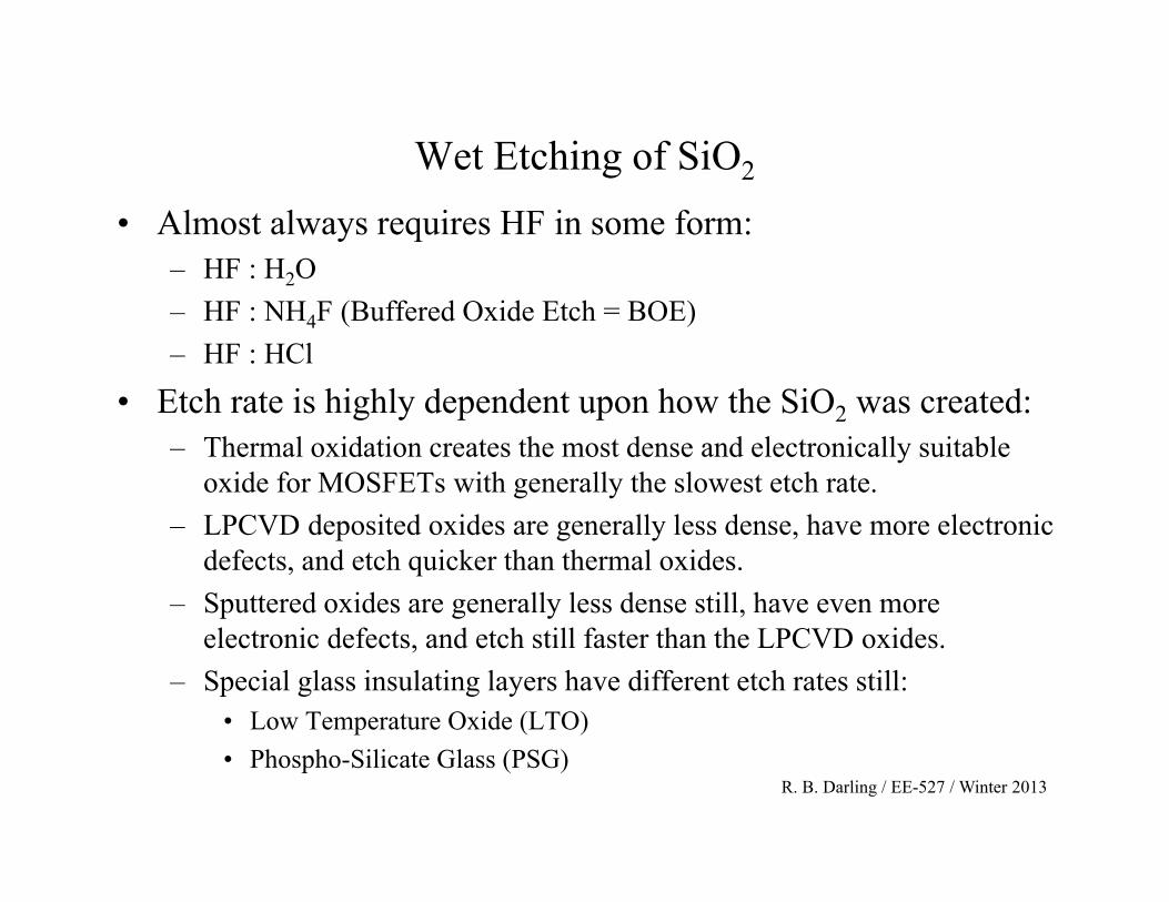
Wet Etching of SiO2
• Almost always requires HF in some form: – HF : H2O– HF : NH4F (Buffered Oxide Etch = BOE)– HF : HCl
• Etch rate is highly dependent upon how the SiO2 was created: – Thermal oxidation creates the most dense and electronically suitable
oxide for MOSFETs with generally the slowest etch rate. – LPCVD deposited oxides are generally less dense, have more electronic
defects, and etch quicker than thermal oxides. – Sputtered oxides are generally less dense still, have even more
electronic defects, and etch still faster than the LPCVD oxides. – Special glass insulating layers have different etch rates still:
• Low Temperature Oxide (LTO)• Phospho-Silicate Glass (PSG)
R. B. Darling / EE-527 / Winter 2013
Buffered Oxide Etch (BOE)
• Normal etching of SiO2 will deplete the F− ion concentration, leading to an etch rate which changes over time.
• This can be fixed by buffering the HF with another source of the F− ion: NH4F.
• Buffering with NH4F also slows the etch rate and results in more polishing of the Si surface (atomically flatter).
• Reactions: – Etching: SiO2 + 6HF H2SiF6 + 2H2O – Buffering: NH4F NH3 + HF
• Many commercial compositions exist: – 5:1, 6:1, 7:1, 10:1, 20:1, 30:1, 50:1, and 100:1. – Ratios are NH4F (40% in H2O) to HF (49% in H2O)
R. B. Darling / EE-527 / Winter 2013
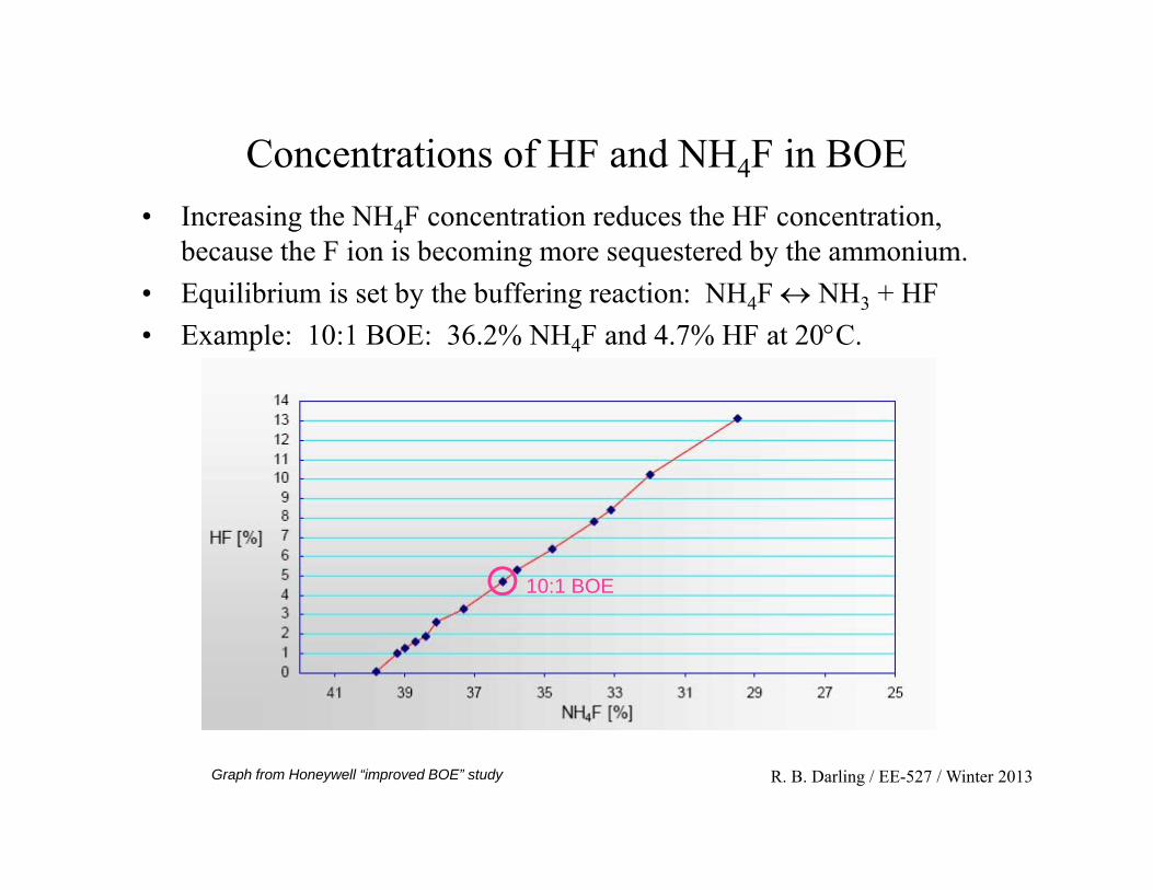
Concentrations of HF and NH4F in BOE• Increasing the NH4F concentration reduces the HF concentration,
because the F ion is becoming more sequestered by the ammonium. • Equilibrium is set by the buffering reaction: NH4F NH3 + HF • Example: 10:1 BOE: 36.2% NH4F and 4.7% HF at 20C.
Graph from Honeywell “improved BOE” study
10:1 BOE
R. B. Darling / EE-527 / Winter 2013
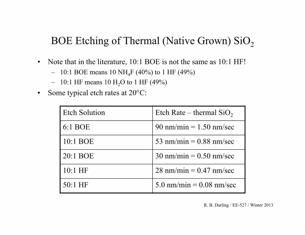
BOE Etching of Thermal (Native Grown) SiO2
• Note that in the literature, 10:1 BOE is not the same as 10:1 HF! – 10:1 BOE means 10 NH4F (40%) to 1 HF (49%) – 10:1 HF means 10 H2O to 1 HF (49%)
• Some typical etch rates at 20C:
Etch Solution Etch Rate – thermal SiO2
6:1 BOE 90 nm/min = 1.50 nm/sec
10:1 BOE 53 nm/min = 0.88 nm/sec
20:1 BOE 30 nm/min = 0.50 nm/sec
10:1 HF 28 nm/min = 0.47 nm/sec
50:1 HF 5.0 nm/min = 0.08 nm/sec
R. B. Darling / EE-527 / Winter 2013
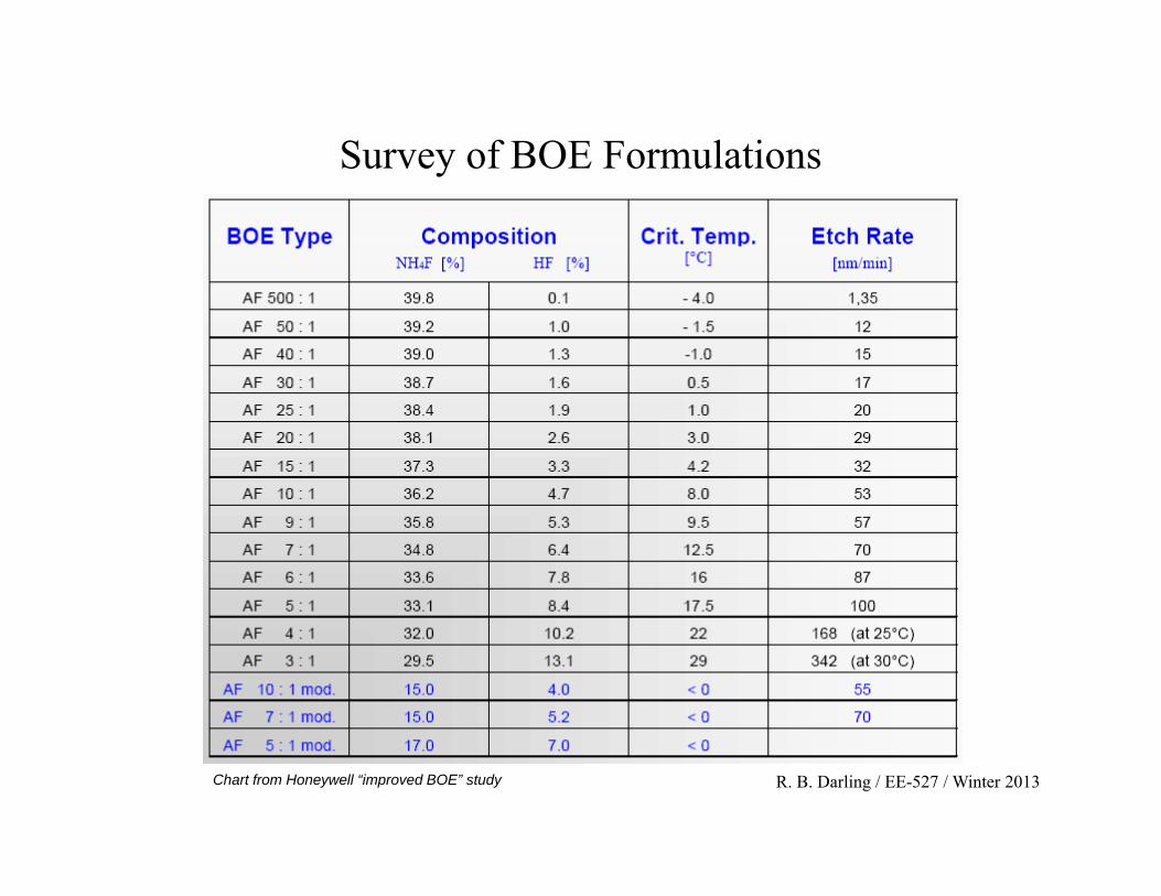
Survey of BOE Formulations
Chart from Honeywell “improved BOE” study
R. B. Darling / EE-527 / Winter 2013
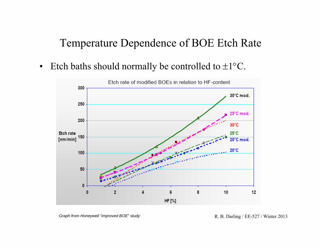
Temperature Dependence of BOE Etch Rate
• Etch baths should normally be controlled to 1C.
Graph from Honeywell “improved BOE” study
R. B. Darling / EE-527 / Winter 2013
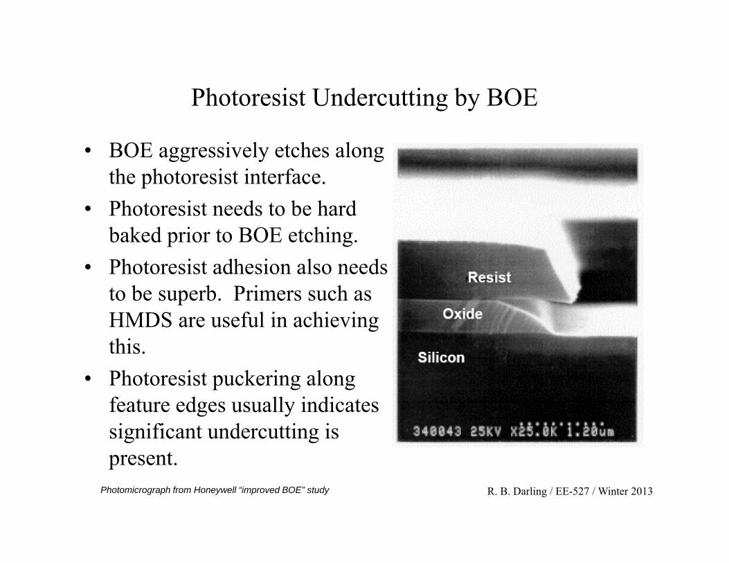
Photoresist Undercutting by BOE
• BOE aggressively etches along the photoresist interface.
• Photoresist needs to be hard baked prior to BOE etching.
• Photoresist adhesion also needs to be superb. Primers such as HMDS are useful in achieving this.
• Photoresist puckering along feature edges usually indicates significant undercutting is present.
Photomicrograph from Honeywell “improved BOE” study
R. B. Darling / EE-527 / Winter 2013
Wet Etches for Contacts and Vias• To increase the interconnect density, contact cuts and vias are usually sized to
the smallest feature limit of the process: 1 x 1 . • Contact cuts and vias usually have “exact size” design rules, and are thus the
smallest feature in a process. • A minimum sized square is the most difficult feature to expose, develop, and
etch without size and shape distortion. • The exact size is necessary to allow the photolithography and etching
processes to be more highly fine tuned so that these features can be reliably created.
• 30-50% over exposure, over development and over etching is often used to guarantee that these processes bottom out inside each contact or via.
• Larger required contact or via areas are created by placing multiple minimum size contacts or vias, rather than making a larger sized one.
• In addition, the contact or via etch often needs to stop on a metal such as aluminum. The etch must be carefully formulated to etch the dielectric and stop on the metal. This can be tricky for wet BOE etching of SiO2 that is covering Al metal.
R. B. Darling / EE-527 / Winter 2013
Wet Etches for Bond and Probe Pads• Pad etches are used to open up the interlevel dielectric and overglass layers
around bonding pads and probe pads. • They are just the opposite of contacts and via cuts: very large single openings. • It is nearly impossible to tune the exposure, development, and etching to
simultaneously preserve feature dimensions on both contacts/vias and pad openings.
– If these features must be done with the same mask, as is often the case, then the process is tuned to the smaller contacts/vias, and the design rules are used to compensate for the overetch that will occur within the pad openings.
• A useful wet pad etch formulation is to dilute the BOE with glycerin, typically 5:3 volume ratio. This produces significantly less etching of the underlying aluminum.
• BOE with surfactants added is usually helpful in getting the etchant down into small contacts and vias, avoiding “blocking” that occurs from surface tension and insufficient wetting of the oxide by the BOE.
R. B. Darling / EE-527 / Winter 2013
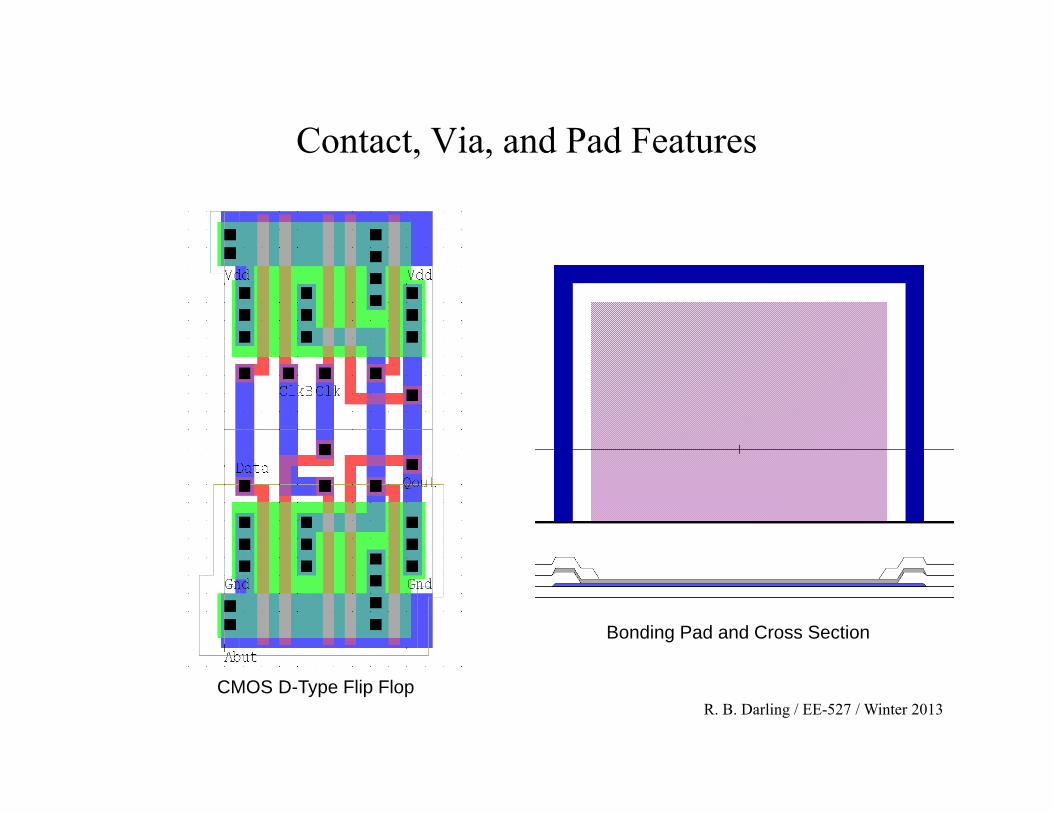
Contact, Via, and Pad Features
CMOS D-Type Flip Flop
Bonding Pad and Cross Section
R. B. Darling / EE-527 / Winter 2013
Wet Etching of Chromium (Cr)
• HCl (standard 37% concentration, undiluted)• HNO3 (standard 70% concentration, undiluted)• Commercial chromium etchants are usually best to achieve
a uniform rate and reproducibility: – Cyantek CR-9 chromium etchant is commonly used.
R. B. Darling / EE-527 / Winter 2013
Wet Etching of Aluminum (Al)
• HCl : H2O @ 1:4• H3PO4 : HNO3 : H2O @ 74:7:19 gives a very rapid etch rate• Almost any of the strong mineral acids with an oxidizer will
etch aluminum: – H2SO4
– HNO3
– HCl– H3PO4
• The trick is usually diluting the acid / oxidizer mixture down to a point to where it can be controllable.
• If the aluminum has a thick skin of Al2O3, this may first have to be removed using an HF-based etchant.
R. B. Darling / EE-527 / Winter 2013
Wet Etching of Gold (Au)
• HCl : HNO3 @ 3:1• Logan’s Gold Etch:
– KI : I2 : H2O @ 1.3 g : 65 g : 100 mL @ room temperature– Etch solution is nearly black and impossible to see wafer once
submerged. – Also etches most compound semiconductors @ ~1.0-2.0 m/min
R. B. Darling / EE-527 / Winter 2013
Wafer Defect Decoration Etches
• Sirtl Etch: 1 part HF (49%) : 1 part CrO3 (5M)• Secco Etch: 2 parts HF (49%) : 1 part K2Cr2O7 (0.15M)• Both of these etches greatly accelerate their etch rate in the
vicinity of crystallographic structural defects such as – Stacking faults– Linear dislocations– Screw dislocations– Twinning
• They leave behind large etch pits which can be easily counted under a microscope to determine the density of these defects. – Etch pit density (EPD) is used as a measure of crystalline quality.
R. B. Darling / EE-527 / Winter 2013
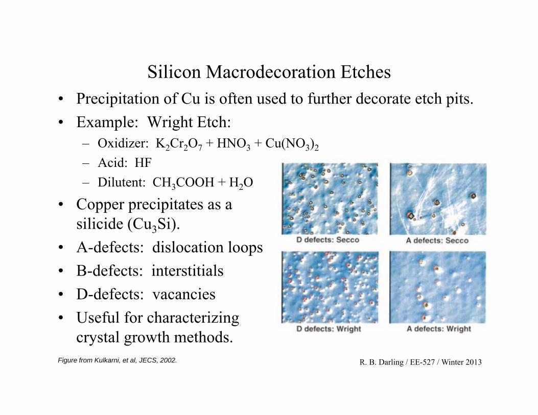
Silicon Macrodecoration Etches• Precipitation of Cu is often used to further decorate etch pits. • Example: Wright Etch:
– Oxidizer: K2Cr2O7 + HNO3 + Cu(NO3)2
– Acid: HF– Dilutent: CH3COOH + H2O
• Copper precipitates as a silicide (Cu3Si).
• A-defects: dislocation loops• B-defects: interstitials• D-defects: vacancies• Useful for characterizing
crystal growth methods. Figure from Kulkarni, et al, JECS, 2002.
R. B. Darling / EE-527 / Winter 2013
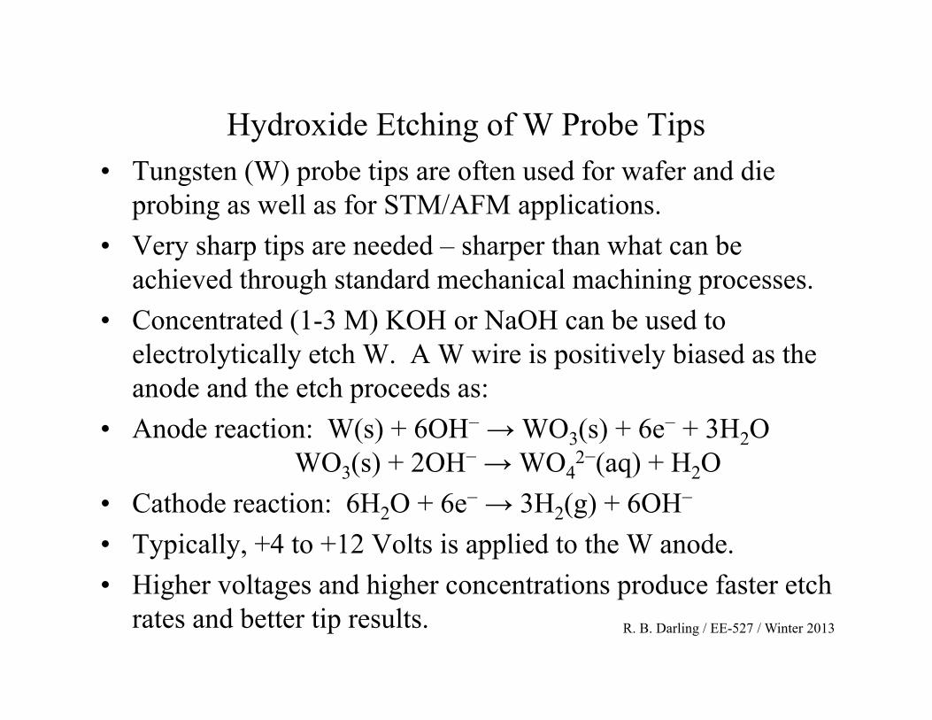
Hydroxide Etching of W Probe Tips• Tungsten (W) probe tips are often used for wafer and die
probing as well as for STM/AFM applications. • Very sharp tips are needed – sharper than what can be
achieved through standard mechanical machining processes. • Concentrated (1-3 M) KOH or NaOH can be used to
electrolytically etch W. A W wire is positively biased as the anode and the etch proceeds as:
• Anode reaction: W(s) + 6OH− → WO3(s) + 6e− + 3H2OWO3(s) + 2OH− → WO4
2−(aq) + H2O• Cathode reaction: 6H2O + 6e− → 3H2(g) + 6OH−
• Typically, +4 to +12 Volts is applied to the W anode. • Higher voltages and higher concentrations produce faster etch
rates and better tip results.
R. B. Darling / EE-527 / Winter 2013
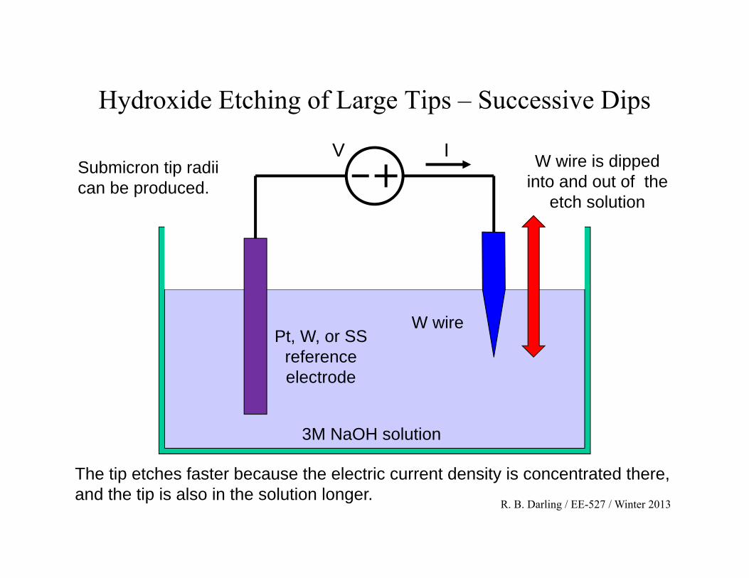
Hydroxide Etching of Large Tips – Successive Dips
Pt, W, or SSreferenceelectrode
3M NaOH solution
V I
W wire
W wire is dippedinto and out of the
etch solution
The tip etches faster because the electric current density is concentrated there, and the tip is also in the solution longer.
Submicron tip radiican be produced.
R. B. Darling / EE-527 / Winter 2013
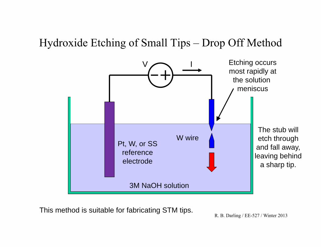
Hydroxide Etching of Small Tips – Drop Off Method
Pt, W, or SSreferenceelectrode
3M NaOH solution
V I
W wire
Etching occursmost rapidly atthe solution
meniscus
The stub willetch throughand fall away,leaving behind
a sharp tip.
This method is suitable for fabricating STM tips.
R. B. Darling / EE-527 / Winter 2013
Techniques for Reproducible Wet Etches
• Design the etch rate for a controllable time period, e.g. several minutes, so that dip and extract times are comparatively short. Dilute the etch if necessary.
• Agitate gently using N2 bubblers, when available. • Use a timer – don’t guess. • Use fresh chemicals. • Control the temperature of the etch bath. • Use a thermometer – don’t guess. • Never mix different substrates within the same etch bath. • Always etch the same thing in the same equipment with
the same chemicals under the same conditions!
R. B. Darling / EE-527 / Winter 2013
Etch Tuning Techniques• For three-part etches (acid/base – oxidizer – dilutent):
– Adjust the overall etch rate through the amount of dilutent while keeping the acid/base – oxidizer ratio constant.
– Adjust the surface finish of the etch through the acid/base –oxidizer ratio while keeping the dilutent fraction constant.
• If necessary, use two etches in sequence: – 1. Roughing etch with a high rate to rapidly remove material. – 2. Finishing etch with a slower etch rate and more polishing action
to produce a higher quality final surface.
• Adjust the etch temperature to balance the reactant transport against the surface reaction rate. – Polishing etches tend to be transport-limited, usually by diffusion. – Roughing etches tent to be surface reaction rate-limited.
R. B. Darling / EE-527 / Winter 2013
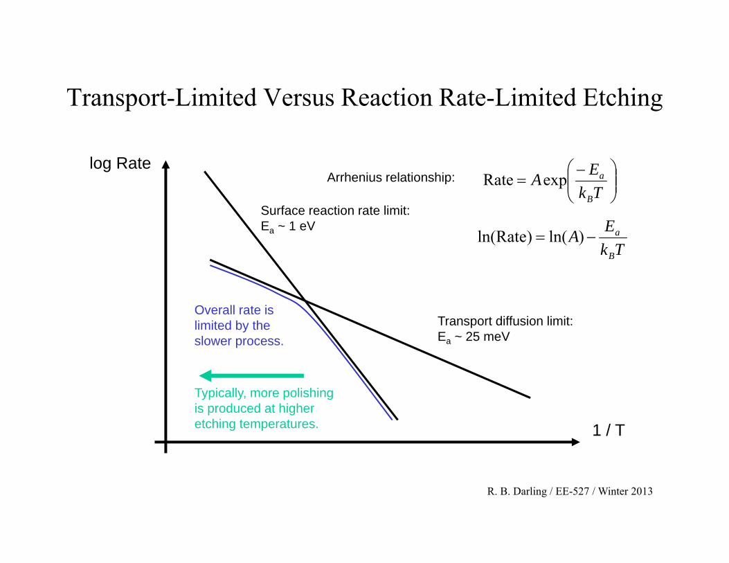
Transport-Limited Versus Reaction Rate-Limited Etching
1 / T
log RateArrhenius relationship:
TkEAB
aexpRate
TkEAB
a )ln()Rateln(Surface reaction rate limit: Ea ~ 1 eV
Transport diffusion limit: Ea ~ 25 meV
Overall rate is limited by the slower process.
Typically, more polishing is produced at higher etching temperatures.
R. B. Darling / EE-527 / Winter 2013
Special Purpose Wet Etching Hardware
• Tanks• Cassettes• Holders and handles• N2 bubble agitators• Quick dumps• Flush and fill systems• Cascade rinsers• Heaters and temperature controllers• Single-sided wafer etching fixtures• Anodic etching fixtures
R. B. Darling / EE-527 / Winter 2013
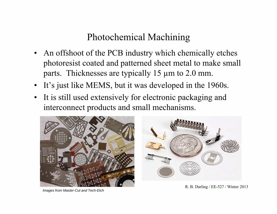
Photochemical Machining• An offshoot of the PCB industry which chemically etches
photoresist coated and patterned sheet metal to make small parts. Thicknesses are typically 15 µm to 2.0 mm.
• It’s just like MEMS, but it was developed in the 1960s. • It is still used extensively for electronic packaging and
interconnect products and small mechanisms.
Images from Master-Cut and Tech-Etch