nanofutures overview and activity 2011
DESCRIPTION
Update of the last activities of the NANOfutures European Technology Platform. Barriers (nodes) for nanotechnology commercialization identifyTRANSCRIPT

Overview of NANOfutures
European Initiative
NANOfutures
association
Margherita Cioffi, D’Appolonia SpANANOfutures CSA Coordinator

NANOfutures is an European Integration and Innovation Platform of which
main objective is to facilitate the nanotechnology development and
commercialization by connecting all relevant nanotechnology stakeholders
(e.g. European Technology Platforms that require nanotechnologies in their
industrial sector and products, industries, research institutions, universities,
associations, regional and national clusters etc.).
NANOfutures will act as a “Nano-Hub” by linking ETPs, JTIs, associations with
expert groups in a collaborative environment.
NANOfutures is an open platform with free access to any nanotechnology
stakeholder.
NANOfutures Initiative
NANOfutures activities are partially sustained by the CSA project funded by
European Commission and entitled “NANOfutures: A cross-ETP Coordination
Initiative on nanotechnology” (Contract No.: NMP4-CA-2010-266789). The
project started in October 2010.

NANOfutures Structure
• The platform is guided and steered by the NANOfutures Steering
Committee (SC), formed by:
• Chair: Paolo Matteazzi, MINAM ETP
• Two co-chairs: Professor Kiparissides (CERTH) and Peter Krüger (Bayer)
• 11 ETP representatives, officially appointed by the ETPs;
• 10 Horizontal working groups chairs.
Steering
Committee
Chair
Two Co-Chairs
FTP Representative
Member
FTP Representative
Member
ETP Representative
MemberScientific Board
Representative
Horizontal group
leader
Scientific Board
Representative
Horizontal group
leader
Scientific Board
Representative
Horizontal group
leaderHorizontal group chair
MemberMember
MemberMember

The aims of NANOfutures CA within the next two years are:
1. to identify and optimize synergies between European and National
Platforms, research programmes, JTI, ERA-NETs and other CSAs
and research projects related to nanotechnology, in order to reduce the
fragmentation of the European nanotechnology and coordinate future
strategies.
2. to identify key strategic nanotechnology nodes addressing issues of
cross-sectional and nano-specific relevance for the innovation and rapid
uptake of nanotechnologies in order to increase EU competitiveness .
3. to construct and disseminate an integrated Industrial and Research
Roadmap for European Nanotechnology, including a medium term
detailed implementation plan.
Strategic Aims

NANOfutures coordinates 10 horizontal Working groups (WG) with
expertise on different areas in nanotechnology:
RESEARCH / TECHNOLOGY
INDUSTRIALIZATION/ nano-MANUFACTURING
COMMUNICATION
SAFETY RESEARCH
INDUSTRIAL SAFETY STRATEGY
INDUSTRIAL NANOSAFETY STRATEGY GROUP
STANDARDIZATION
REGULATION
TECHNOLOGY TRANSFER and INNOVATION FINANCING
NETWORKING
SKILLS AND EDUCATION
NANOfutures Working Groups
From the interaction of these WG with industrial sector representatives
coming from European Technology Platforms, the strategic key nodes in
terms of cross-sectorial research, development and innovation as well as
socio-economical challenges were indentified

ETP representatives in NANOfutures
11 ETPs signed the Memorandum of Understanding, in order to declare their
support to NANOfutures. These ETPs are representative of several industrial
sectors and were the ones interacting with the WGs:
Textiles (FTC);
Nanomedicine (NANOMEDICINE);
Chemistry (SusChem);
Construction (ECTP);
Nanoelectronics (ENIAC);
Nanomanufacturing (MINAM and MANUFUTURE);
Transportation (ERTRAC);
Advanced engineering materials and technologies ( EUMAT);
Photonics (PHOTONICS21);
Industrial Safety (ETPIS).

Horizontal
Working Groups
(e.g. NANOSAFETY,
STANDARDISATION
, REGULATION etc.)
ETP needs (e.g. SUSCHEM , MANUFUTURE,
PHOTONICS 21, EUMAT, FTC, MINAM etc. )
KEY NODES:
Nanotechnology
nodes related to
several sectors and
different horizontal
issues.
Methodology
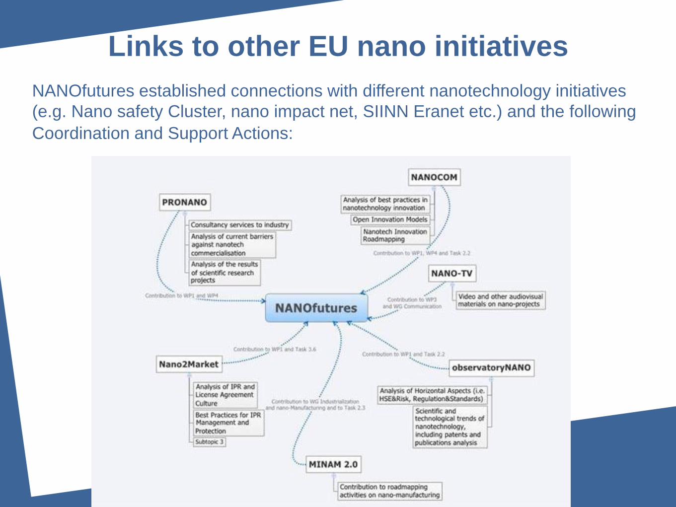
Links to other EU nano initiatives
14
NANOfutures established connections with different nanotechnology initiatives
(e.g. Nano safety Cluster, nano impact net, SIINN Eranet etc.) and the following
Coordination and Support Actions:

NANOfutures Today
14

NANOfutures members
• NANOfutures today
has 420 members
• ~31% of them are
industry
Update: 3 May 2011
0
1-5
5-10
10-30
30-60
60+
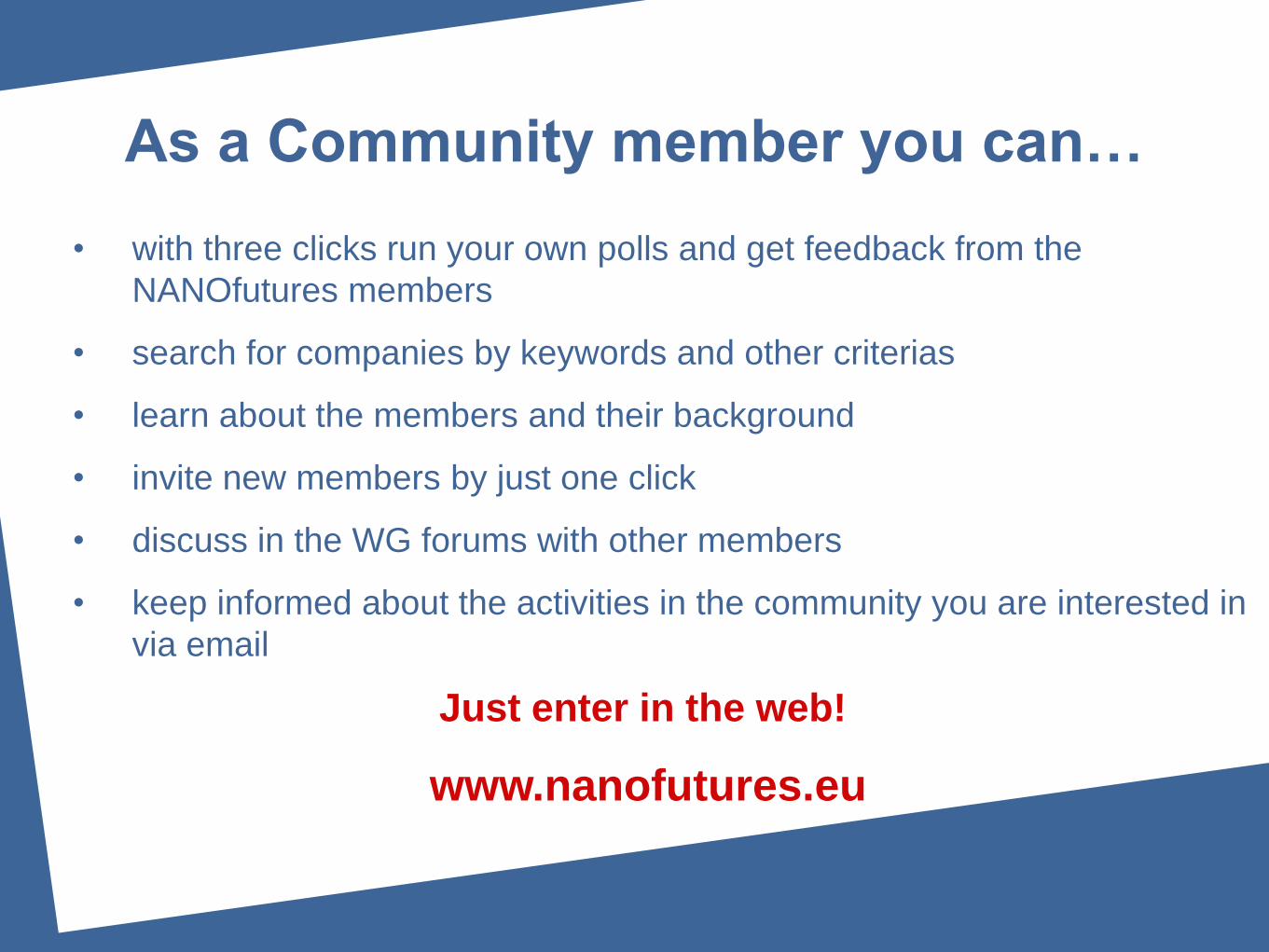
As a Community member you can…
• with three clicks run your own polls and get feedback from the
NANOfutures members
• search for companies by keywords and other criterias
• learn about the members and their background
• invite new members by just one click
• discuss in the WG forums with other members
• keep informed about the activities in the community you are interested in
via email
Just enter in the web!
www.nanofutures.eu

Activities performed so far: Timeline
September, Start NANOfutures CSA
19 October, Kick off, Working Group Leaders, collection of ETP needs
November, complete list of ETP-needs disseminated to WG
20 January, Working Groups Meeting, Clusterisation
Definition, Evaluation Grids disseminated to the
WG participants
15 March, WG Technical Meeting, Definition of Key-Nodes
14 April, Steering Commettee, Approval of Key-Nodes
May, Definition of Inventive Sessions Groups

Brussels, 15 March 2011
WG Technical Meeting
Industrialization
and Manufacturing WG
Clustering of inputs – potential nodes
November 2011
ETP representative direct
input regarding their needs:
50 ETP inputs from
FTC
ECTP
ENIAC
ERTRAC
ETPIS
EUMAT
MANUFUTURE
MINAM
NANOMEDICINE
PHOTONICS 21
SUSCHEM
11 Working Groups, Identification of actions
to address clustered ETP needs :•RESEARCH / TECHNOLOGY
•INDUSTRIALIZATION/ nano-MANUFACTURING
•COMMUNICATION
•SAFETY RESEARCH
•INDUSTRIAL SAFETY STRATEGY
•STANDARDIZATION
•REGULATION
•TECHNOLOGY TRANSFER and INNOVATION
FINANCING
•NETWORKING
•SKILLS AND EDUCATION
Working Group Meeting
20 January, Brussels
Activities performed so far: Scheme
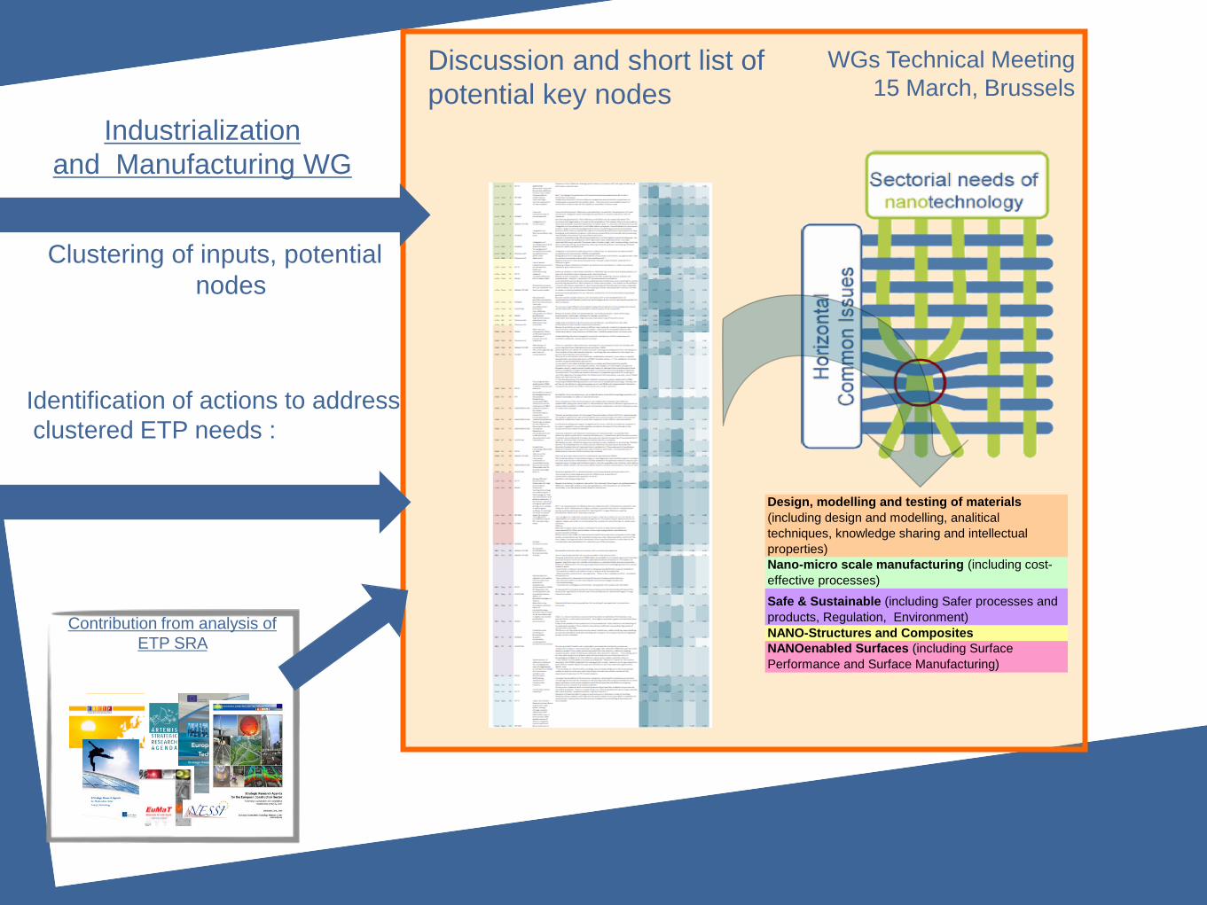
Contribution from analysis of
ETP SRA
Clustering of inputs, potential
nodes
Industrialization
and Manufacturing WG
Identification of actions to address
clustered ETP needs :
Discussion and short list of
potential key nodes
Design, modelling and testing of materials
(including design and modelling, analitical
techniques, knowledge sharing and intellectual
properties)
Nano-micro scale manufacturing (including cost-
effective processes)
Safe & Sustainable (including Safer processes and
products, Regulation, Environment)
NANO-Structures and Composites
NANOenabled Surfaces (including Surface
Performance and Surface Manufacturing)
WGs Technical Meeting
15 March, Brussels
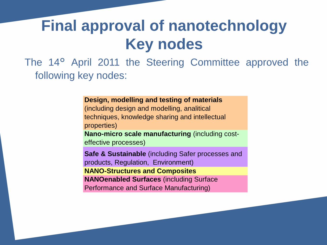
Final approval of nanotechnology
Key nodesThe 14° April 2011 the Steering Committee approved the
following key nodes:
Design, modelling and testing of materials
(including design and modelling, analitical
techniques, knowledge sharing and intellectual
properties)
Nano-micro scale manufacturing (including cost-
effective processes)
Safe & Sustainable (including Safer processes and
products, Regulation, Environment)
NANO-Structures and Composites
NANOenabled Surfaces (including Surface
Performance and Surface Manufacturing)

Design, Modelling and
Testing of materials
Nano-Micro scale
manufacturing
Safe & Sustainable
Nano structures and
compositesNano-enabled
surfaces
COATINGS
HIGH PERFORMANCE
SENSORS
FUNCTIONALISATION
PRODUCTION
CHARACTERIZATION
PRACTICE GUIDELINES
HEALTH
REGULATION
ENVIRONMENT
MEASUREMENT PROTOCOLS
NANO-MICRO SCALE
INTEGRATION
BOTTOM-UP
HIGH VOLUME
TOP-DOWN
PRODUCTION LINES
COST
CHARACTERIZATION
MODELLING
LIFE CYCLE
DESIGN
CLASSIFICATION
PATENTING
COMPOSITES
ACCURACY
HIGH YELD
2D CONTROL
INTEGRATION
On these key nodes NANOfutures will define the Industrial
and Research Roadmap for European Nanotechnology

• Design, Modelling and Testing of materials: includes design of
nanomaterials from concept to disposal and recycling, modelling, characterization,
toxicity tests. Knowledge management including patenting, availability of knowledge
repository on nanomaterial safety etc. From ETP needs: ENIAC, Photonics21,
MANUFUTURE, EUMAT, ETPIS, FTC, NANOMEDICINE, SUSCHEM.
• Nano-Micro scale manufacturing: includes low cost and high efficient
production of nanomaterials, nanoobjects, nanoparticles multi scale fabrication and
scale-up processes. From ETP needs: EUMAT, MANUFUTURE, MINAM,
Photonics21, ECTP, ENIAC, SUSCHEM, NANOMEDICINE
• Safe & Sustainable: includes standards & best practise guidelines for
handling nanomaterials (nanoparticles, nanopowders), measurement protocols for
nanomaterials; risk assessment and risk management; environmentally friendly and
sustainable nanomaterials production processes. From ETP needs: MANUFUTURE,
ETPIS, SUSCHEM, FTC, ENIAC, MINAM, NANOMEDICINE.
Final approval of nanotechnology
Key nodes

• Nano structures and composites: High yield, low dispersion, high
accuracy manufacturing of nanostructures; up-scaling from lab to industrial
processes; ultra-high performance composites with smart properties for different
applications. From ETP needs: ENIAC, Photonics21, ECTP, FTC, ERTRAC,
MANUFUTURE, NANOMEDICINE.
• Nano-enabled surfaces: nanocoating technologies and manufacturing for
smart surfaces (energy efficient, high performance, active, sensing etc.). From ETP
needs: ECTP, ENIAC, ERTRAC, EUMAT, MINAM.
The proposed key nodes are interconnected and there are horizontal actions which
should link together such needs: e.g. communication and networking,
standardization, cost optimization, research on smart properties of nanomaterials.
Final approval of nanotechnology
Key nodes

What to do next:
the perspective
Final list of key nodes
Inventive Sessions
Workshops on each key node
(June2011 -January 2012)
Targets
and Challenges
Industrial and Research
Roadmap
(March- June 2012)
Dissemination, Exploitation and
networking activities
Approval of a list of
key nodes
Definition of the expert groups
One Group for each
Key-Node
Working Groups
Review of inventive session
results and feedback
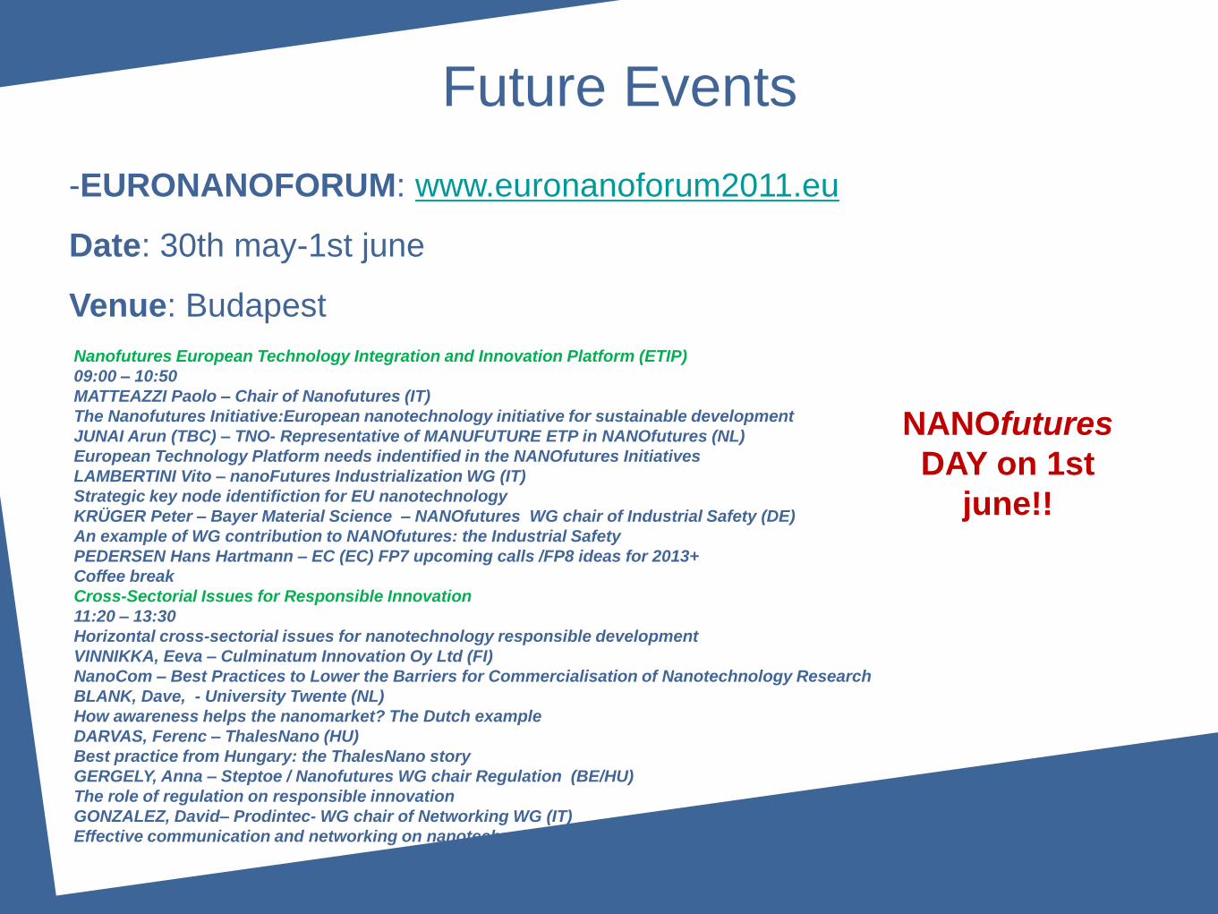
Future Events
-EURONANOFORUM: www.euronanoforum2011.eu
Date: 30th may-1st june
Venue: Budapest
Nanofutures European Technology Integration and Innovation Platform (ETIP)
09:00 – 10:50
MATTEAZZI Paolo – Chair of Nanofutures (IT)
The Nanofutures Initiative:European nanotechnology initiative for sustainable development
JUNAI Arun (TBC) – TNO- Representative of MANUFUTURE ETP in NANOfutures (NL)
European Technology Platform needs indentified in the NANOfutures Initiatives
LAMBERTINI Vito – nanoFutures Industrialization WG (IT)
Strategic key node identifiction for EU nanotechnology
KRÜGER Peter – Bayer Material Science – NANOfutures WG chair of Industrial Safety (DE)
An example of WG contribution to NANOfutures: the Industrial Safety
PEDERSEN Hans Hartmann – EC (EC) FP7 upcoming calls /FP8 ideas for 2013+
Coffee break
Cross-Sectorial Issues for Responsible Innovation
11:20 – 13:30
Horizontal cross-sectorial issues for nanotechnology responsible development
VINNIKKA, Eeva – Culminatum Innovation Oy Ltd (FI)
NanoCom – Best Practices to Lower the Barriers for Commercialisation of Nanotechnology Research
BLANK, Dave, - University Twente (NL)
How awareness helps the nanomarket? The Dutch example
DARVAS, Ferenc – ThalesNano (HU)
Best practice from Hungary: the ThalesNano story
GERGELY, Anna – Steptoe / Nanofutures WG chair Regulation (BE/HU)
The role of regulation on responsible innovation
GONZALEZ, David– Prodintec- WG chair of Networking WG (IT)
Effective communication and networking on nanotechnology
NANOfutures
DAY on 1st
june!!

Future Events
• NanotechItaly 2011: http://www.nanotechitaly.it/
Date: November 23-25, 2011
Venue: Venice, Italy:
Nfts activities:
-In the plenary session of the 23rd a 1h session (4 presentations) dedicated
to EU and IT NANOfutures platform is foreseen.
-next Steering Committe and WG Meetings
-Technology transfer event (to be confirmed) .

Contacts
For information on NANOfutures activities, please contact NANOfutures CSA Coordinator:
Margherita Cioffi,
D’Appolonia S.p.A.
Largo Carlo Salinari, 18/19 – 00142 Rome – Italy
www. nanofutures.eu