notes on the lecture logical design of digital...
TRANSCRIPT

NNootteess oonn tthhee lleeccttuurree
LLooggiiccaall DDeessiiggnn
ooff
DDiiggiittaall SSyysstteemmss PPrrooff.. DDrr..--IInngg.. AAxxeell HHuunnggeerr
DDrr..--IInngg.. SStteeffaann WWeerrnneerr
UNIVERSITÄT
D U I S B U R G E S S E N
© Institute of Computer Engineering,
Dr.-Ing. Stefan Werner, June 2009

1. INTRODUCTION ........................................................................................................ 4
2. ELEMENTARY COMBINATORIAL CIRCUITS FOR DATA TRANSMISSION ......................................................................................................... 5
2.1 Buses .............................................................................................................................. 8
2.2 Multiplexer ..................................................................................................................... 9
2.3 Demultiplexer ................................................................................................................ 10
2.4 Decoders ....................................................................................................................... 11
2.5 Bidirectional Signal Traffic .......................................................................................... 12 2.5.1 Wired Or ................................................................................................................... 13 2.5.2 Tri-State Technology ................................................................................................ 15 2.5.3 Bus Signals ................................................................................................................. 16 2.5.4 Bidirectional bus drivers ........................................................................................... 18
3. MEMORY UNITS ...................................................................................................... 19
3.1 Memory addressing ...................................................................................................... 20 3.1.1 Word-based addressing ............................................................................................ 21 3.1.2 Bit-wise addressing .................................................................................................. 23
3.2 RAMs and ROMs ......................................................................................................... 23 3.2.1 Random Access Memories (RAMs) ......................................................................... 24
3.2.1.1 Static RAMs (SRAM) ...................................................................................... 25 3.2.1.2 Dynamic RAMs (DRAM) ................................................................................ 29
3.2.2 Read Only Memory (ROM) ..................................................................................... 29 3.2.2.1 The Mask ROM ................................................................................................ 30
4. PROGRAMMABLE LOGIC DEVICES ................................................................. 33 4.1 General structure .......................................................................................................... 33
4.2 Construction of the AND/OR-Matrix ........................................................................... 36
4.3 Types of Illustrations .................................................................................................... 39
4.4 Programming Points ..................................................................................................... 41
4.5 PLD Structures ............................................................................................................. 43 4.5.1 Combinatorial PLD .................................................................................................. 43
4.6 Logic Diagram .............................................................................................................. 46
4.7 Functional Block Diagram ........................................................................................... 48
4.8 Logic-Circuit Symbols ................................................................................................. 49
4.9 The Programming of the PLD ...................................................................................... 50 4.9.1 Combinatorial PLD with Feedback .......................................................................... 51 4.9.2 Special Features of Feedback ................................................................................... 52 4.9.3 Functional Block Diagram ....................................................................................... 55
5. ALGORITHMIC MINIMIZATION APPROACHES ........................................... 56 5.1 Minimization of combinational Functions ................................................................... 56

5.1.1 The Quine / McCluskey algorithm ........................................................................... 60 5.1.2 Cost functions ........................................................................................................... 68 5.1.3 Petrick’s method ....................................................................................................... 69 5.1.4 Proceeding in combinational circuit synthesis ......................................................... 72
5.2 State machine minimization ......................................................................................... 72 5.2.1 Repetition: State Machines ....................................................................................... 73 5.2.2 Forms of Describing State Machines ....................................................................... 74
5.2.2.1 State machine tables ......................................................................................... 74 5.2.2.2 State-Transition Diagram ................................................................................. 76 5.2.2.3 Timing Diagram ............................................................................................... 78
5.2.3 Trivial state machine minimization .......................................................................... 79 5.2.4 Minimization according to Huffmann and Mealy .................................................... 81 5.2.5 The Moore Algorithm ............................................................................................... 84 5.2.6 Algorithmic Formulation of the Minimization by Moore: ....................................... 86
5.3 Conversion of State Machines ...................................................................................... 88
6. ELEMENTARY SEQUENTIAL CIRCUITS AND SEQUENTIAL CIRCUIT DESIGN AND ANALYSIS ........................................................................................ 92
6.1 Design of synchronous counters ................................................................................... 94
6.2 Design of asynchronous counters ............................................................................... 100
6.3 Shift registers .............................................................................................................. 102
7. TESTING DIGITAL CIRCUITS ........................................................................... 106 7.1 Introduction ................................................................................................................ 106
7.2 Principles of testing .................................................................................................... 109
7.3 Overview on test mechanisms .................................................................................... 112 7.3.1 Important CAD-tools for test generation ................................................................ 113 7.3.2 Application of test-tools in integrated systems ...................................................... 114
7.4 Faults and fault-models .............................................................................................. 115 7.4.1 The Stuck-at fault-model ........................................................................................ 117
7.5 Test generation ........................................................................................................... 120 7.5.1 Boolean Difference ................................................................................................. 120 7.5.2 Path-sensitization .................................................................................................... 124

1. Introduction
This course covers a subtopic of the development process of digital systems, which is the logical design. Physical or electrical design e.g. deals with dimensioning of transistors or layouts for printed circuit boards, whereas logical design focuses more on functional aspects of digital systems. The lectures in “Logical Design of Digital Systems” can be seen as an extension of the topics discussed in the 1st semester in the lectures “Fundamentals of Computer Engineering 1”, which can be seen as a requirement to follow the “Logical Design of Digital Systems” lecture. The lecture notes of „logical Design in Digital System“ give an overview of the topics presented in the lectures since summer semester 2009. Even if the text is carefully edited and reviewed students shall use it carefully and critically. Students are asked to use it in parallel to the lectures, it can not be seen as a substitute to attend the lectures or the usage of other books and sources

5
2. Elementary combinatorial circuits for data transmission
Inside a computer system, the data transfer plays a significant role especially in the operational part. So called transmission networks connect the single units in a computer and switch the necessary information to them without manipulation. According to this, data transmission is an operation that is not dependent on data-types. Multiplexers and demultiplexers are used for selection of paths, functions or devices. The actual transmission occurs on bus-lines.
Figure 2.1: General Bus Structure
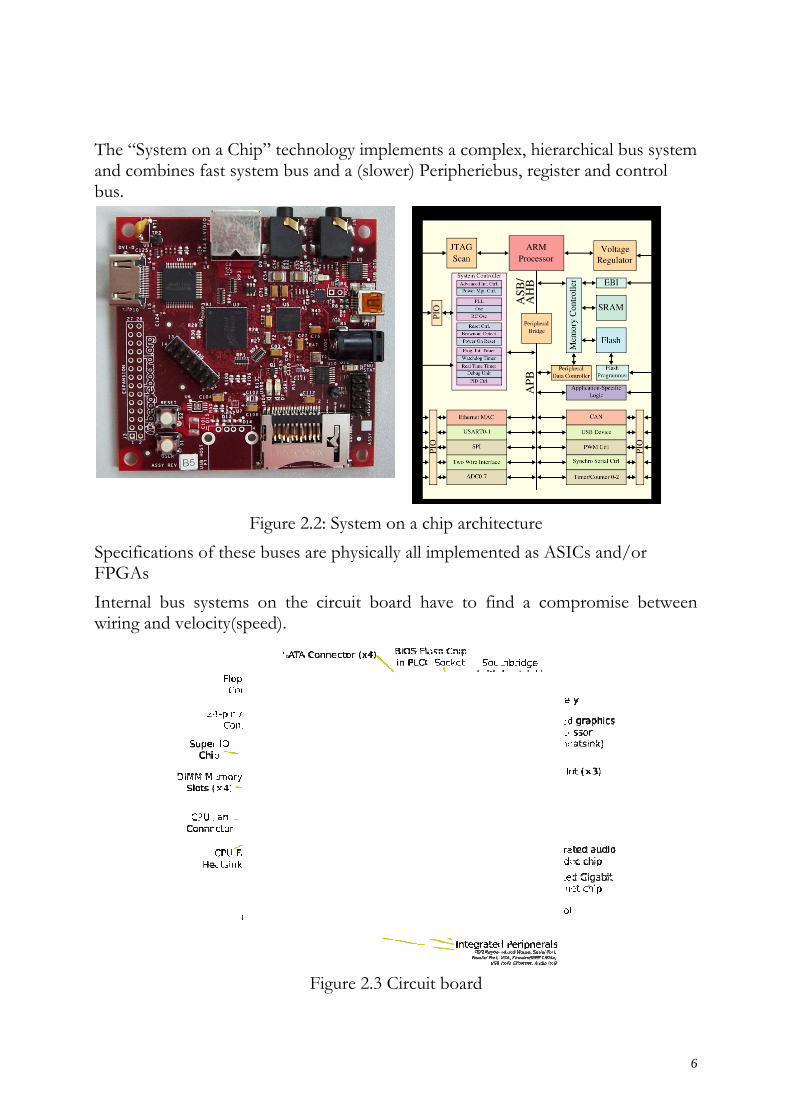
A bus can be thought of as a “highway” for digital signals. It consists of a set of physical connections (printed circuit traces or wires), standard set of specifications that designate the characteristics and types of signals that can travel along the pathway. Buses are found on all levels of a computer system. They fulfill different tasks in the process, from which different properties and construction characteristics result. In the following some examples are given. a.) Internal buses
Internal buses interconnect the various components within a computer system, processor, memory, interface cards, etc
The “Sand cobus.
SpecifiFPGAInternawiring
System on mbines fas
cations of s al bus sysand veloci
a Chip” test system b
Figurf these bus
tems on tity(speed).
echnology bus and a
re 2.2: Systes are phy
the circuit
Figure
implemen(slower) P
tem on a cysically all i
t board h
2.3 Circui
nts a compPeripherieb
chip architeimplement
have to fin
it board
plex, hierarbus, registe
ecture ted as ASI
nd a comp
rchical bus er and cont
Cs and/or
promise b
6
system trol
r
between

7
b.) External or I/O buses
External buses transfer digital signals between a computer and the “outside word” and/or interface the computer with peripheral equipment. They also support standardization and exchangeability of components in a system.
Figure 2.4: External bus systems
c) Computer network
Bus systems in a computer network aim at little wiring and use special protocols for securing data traffic. All systems are connected to the bus If groups of machines communicate at the same time; collisions occur. Special arbitration approaches like CSMA/CD help to solve these problems.
Figure 2.5: Bus system in a computer network

8
2.1 Buses
Buses connect spatially distributed information sources (Sender) and –sinks (Receiver) via decentralized multiplexers and demultiplexers, often combined with decentralized coding and decoding. A bus is therefore a component for the transportation of information. In computers the microprocessor controls and communicates with the memories and the I/O devices via the internal bus structure. The bus is multiplexed so that any of the devices connected to it can either send or receive data to or from the other devices. At any given time, there is only one source active and sending data to one of the components. The selection is under control of the microprocessor.
Figure 2.6 Basic multiplexed bus
From a functional point of view a bus is a node with switches arranged in a star topology. From the technical point of view it is a line with switches for the connection (of pairs) of Senders and Receivers.
left: technical Structure (due to wired logic bidirectional information flow
right: logic equivalent (without wired logic, mono-directional information flow)
Figure 2.7: Principle Circuit and Functionality of Bus Systems Figure 7 shows on the left side a Bus, which connects the Sender (Index S) and the Receiver (Index E) from six system components (A to F) with each other. Due to
9
the multiplexer function of this Bus, only one source is allowed to send, i.e. all of them switch its information on the Bus. The sinks are each according to their function not equipped with gates, i.e. always receive the information. Or they are equipped with gates and only receive the information when they are chosen. Buses are categorized in unidirectional and bidirectional buses. Unidirectional buses only have one source or one sink, i.e. information is forwarded only in one direction along the transmission line. In case of a bidirectional bus, information can be forwarded in both directions.
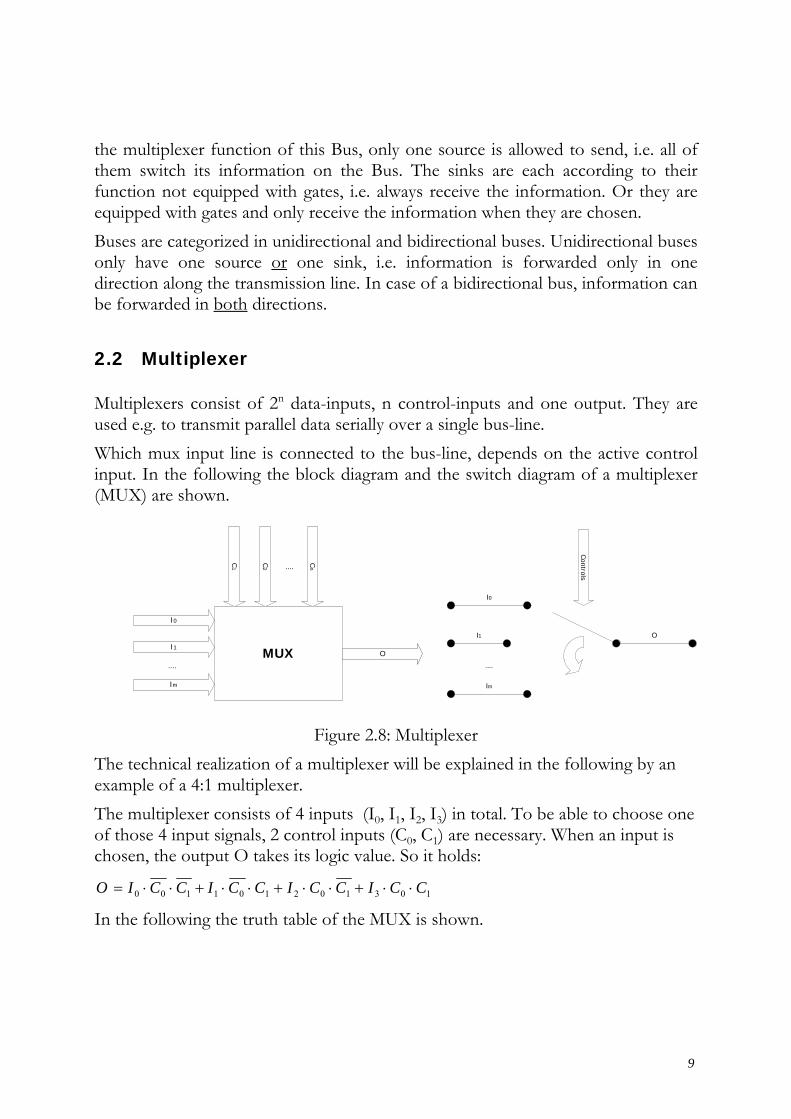
2.2 Multiplexer
Multiplexers consist of 2n data-inputs, n control-inputs and one output. They are used e.g. to transmit parallel data serially over a single bus-line. Which mux input line is connected to the bus-line, depends on the active control input. In the following the block diagram and the switch diagram of a multiplexer (MUX) are shown.
MUX
I0
I1
Im
....
C1
C2
Cn....
O
I0
I1
Im
....
O
Controls
Figure 2.8: Multiplexer The technical realization of a multiplexer will be explained in the following by an example of a 4:1 multiplexer. The multiplexer consists of 4 inputs (I0, I1, I2, I3) in total. To be able to choose one of those 4 input signals, 2 control inputs (C0, C1) are necessary. When an input is chosen, the output O takes its logic value. So it holds:
103102101100 CCICCICCICCIO ⋅⋅+⋅⋅+⋅⋅+⋅⋅=
In the following the truth table of the MUX is shown.

10
I0 I1 I2 I3 C0 C1 O 0 X X X 0 0 0 1 X X X 0 0 1 X 0 X X 0 1 0 X 1 X X 0 1 1 X X 0 X 1 0 0 X X 1 X 1 0 1 X X X 0 1 1 0 X X X 1 1 1 1
Table 2.1: Truth table of a 4-1 multiplexer
2.3 Demultiplexer
The counterpart of the MUX is the demultiplexer. The DeMUX e.g.
• distributes serial input-data to one of several parallel outputs.
• does a 1-out-of-n selection Therefore it has one data-input, n control-inputs and 2n data-outputs.
O0
O1
Om
....
I
Controls
Figure 2.9: Demultiplexer a) schematic and b) functionality

11
C0 C1 I O0 O1 O2 O3 0 0 0 0 0 0 0 0 0 1 1 0 0 0 0 1 0 0 0 0 0 0 1 1 0 1 0 0 1 0 0 0 0 0 0 1 0 1 0 0 1 0 1 1 0 0 0 0 0 1 1 1 0 0 0 1 Table 2.2: Truth table for a 1-4 Demultiplexer
0 0 1O C C I= 1 0 1O C C I= 2 0 1O C C I= 3 0 1O C C I=
2.4 Decoders
If the DeMUX has no data input it is called decoder and can be used to
select one out of n components, e.g. for sending or receiving from a bus.
Figure 2.10: Bus system with decoders
12
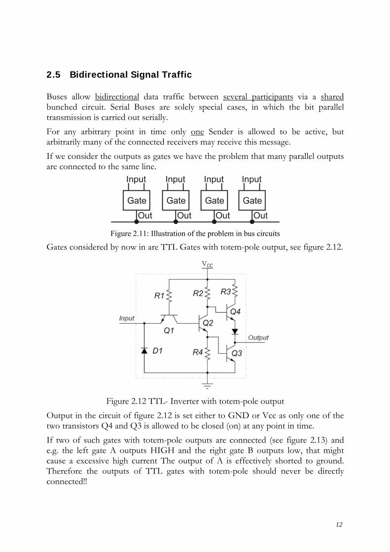
2.5 Bidirectional Signal Traffic
Buses allow bidirectional data traffic between several participants via a shared bunched circuit. Serial Buses are solely special cases, in which the bit parallel transmission is carried out serially. For any arbitrary point in time only one Sender is allowed to be active, but arbitrarily many of the connected receivers may receive this message. If we consider the outputs as gates we have the problem that many parallel outputs are connected to the same line.
Figure 2.11: Illustration of the problem in bus circuits
Gates considered by now in are TTL Gates with totem-pole output, see figure 2.12.
Figure 2.12 TTL- Inverter with totem-pole output
Output in the circuit of figure 2.12 is set either to GND or Vcc as only one of the two transistors Q4 and Q3 is allowed to be closed (on) at any point in time. If two of such gates with totem-pole outputs are connected (see figure 2.13) and e.g. the left gate A outputs HIGH and the right gate B outputs low, that might cause a excessive high current The output of A is effectively shorted to ground. Therefore the outputs of TTL gates with totem-pole should never be directly connected!!

13
Figure 2.13: Connection of two totem-pole outputs
In other words, to connect the outputs of several gates to the same line, special switching techniques are necessary, which will be described in the following.
2.5.1 Wired Or
Another type of output available in TTL is the open-collector output. In this type the output is the transistors collector with nothing connected to it, hence the name open collector. In order to get the proper HIGH, LOW logic levels out of the circuit, an external pull-up resistor must be connected to Vcc from the collector of Q3
Figure 2.14 Open collector output
In figure 2.14 b the output is pulled up to Vcc through the external resistor when Q3 is off. If Q3 is on, the output is connected to near-ground through the saturated transistor. Outputs of gates with open-collector-output can directly be connected to the same line. Figure 2.15 gives an example of an open-collector wired negative AND operation with Inverters

14
Figure 2.15 Open collector circuits
Figure 2.16: wired NAND
The open collector technique can also be used to connect several devices to a bus line. The initial problem can be solved in a way , that for all outputs the output resistor against the operating voltage is cancelled, and instead of this externally is connected to the line. Then each switching level can switch the voltage on the bus line to ground potential. The connection of several drivers on the Bus occurs as an exception via the direct connection of the Gate outputs and connection with an external Pull-up-resistor.
AR
V
T
T
T
CC
1
2
3
Fig. 2.14: Wired-Or
- As soon as at least one Transistor is active, A = 0 (UA ≈ 0,2V)
- When all transistors block , A = I (UA ≈ VCC)
- A transistor is active when UBE > 0,7 V
- A transistor is blocked, when UBE ≤ 0,7 V
- UBE is a result of the logic connection of the inputs of the individual gates
As a further agreement, it must be fixed for the definition of the bus circuit that, for non active senders the output transistors are blocked (i.e. switching on, a logic I on the bus) so that the active driver alone takes a decision on the state of the bus line.

15
Advantage: - simple switching techniques Disadvantage: - The driver capacity for logic I is low (solely over R).
- Small values of R or a big number of inputs switched on later, lead to slow signal flanks and therefore delays.
2.5.2 Tri-State Technology
Another option to ensure that only one component is controlling the voltage of the bus line is, to modify the output lines of all components in a way that all of them are disconnected from the bus line, except the one that is controlling the bus line. In that case all output components have to be modified in such a way that an additional signal OE (Output Enable) separates the output component from the bus line when the unit is not selected. The output line shows in this case non of the defined voltages to assign a logical “0” or “I” to the logical output. In doing so, a third state is defined; the high impedance. Should exactly this component be selected, then short cuts in the circuit will certainly be avoided. Since every output line can now be in exactly one of three possible states ( writing a “0” on the bus, writing a “I” on the bus; cut off from bus), we now also speak about tri-state outputs, i.e. tri-state drivers respectively. The choice of components on the bus, which can write on the bus, can for example occur via a decoder component, since it has been determined that for this component, a “I” always only lies on one of its outputs. The respective signals must be made readily available by the bus management. Buses with tri-state drivers have three states: “0” (Low), “I” (High), “Z” (Z=high impendent). In contrast to open-collector buses, the states L and H will be handled symmetrically. The tri-state bus is faster than the open collector bus, it requires however a higher implementation complexity.
Fig. 2.15: Tri-State Gate as Circuit diagram

16
OE D O 0 0 Z OE = 0 disconnects the output line by O=Z 0 I Z I 0 I OE = I enables the output line. Gate operates in inverse mode I I 0 O = D .
In a tri-state bus it is never allowed to have two participants simultaneously active. Otherwise, this can lead to damaging of the bus, when a participant wants to drive a bus line on H (laying on the operating voltage), and others want to drive it on L (laying it on mass). Therefore tri-state drivers are used for bus lines which only become active after the arbitration e.g. address-and data lines. Advantages :
- simple switching technology for the user
- Actively operated 0- and I-states (high fan out).
- Also for numerous drivers per line, no disadvantages in the time behaviour. Disadvantages: In case mistakenly two drivers are activated simultaneously
- an undefined voltage level can appear on the bus line,
- there exists a danger of destruction due to disallowed high transverse currents.
The tri-state technology has established itself in computer manufacturing in comparison to the Open-Collector-Technology.
2.5.3 Bus Signals
Now we want to focus on the control part of a bus circuit. Assuming the usage of a tristate register, a special input (signal) OE is needed that controls the output lines and allows the register to send data to the data bus. Further more a special input (signal) IE selects the register and allows to read data from the data bus. These signals are to be generated by a special control unit, e.g. microprocessor, decoder, etc.

17
Example: Reading data from the bus
To read data from the data bus, the output of all components, except for the sender, have to be set to high impedance, therefore for all of these components a signal OE 1 has to be generated. To allow components to read, the inputs of the respective components have to be enabled with IE 0. In the diagram in figure 2.16 this happens at t1.Then, the reading starts with the next clockpulse at t2. The condition t2 > t1 has to be fulfilled to ensure that all effects like delay, rising, falling are done, and the signals on the bus lines are stable.
Figure 2.16: Reading data from a bus line
A simplified way to show the same signal activity on the bus line combines the single bus lines to a bundle, see figure 2.17.
Figure 2.17: simplification in bus timing diagramms

18
2.5.4 Bidirectional bus drivers
In most systems bidirectional signal traffic is allowed and therefore bidirectional bus drivers are needed that ensure that a component at any point in time is allowed either to send or receive data. Such a system configuration is shown in figure 2.18.
System2
System3
System1
1
1
1
1
1
1
EEE 12 3 Ei: centrally controlled by the main system
Figure 2.18: Bidirectional signal traffic The Enable-Signals Ei are in most cases under central control of a central system. A combination of tri-state-technology and direction switching results in the frequently used bidirectional bus drivers:
&
&
& &
1
1
D
D
R
A1
2
E
E R path function0 0 A -> D2 receive0 I D1 -> A send I 0 A = Z passive D2 = Z I I A = Z active D2 = Z
Table 2.4
E : shared Enable; R: definition of direction Figure 2.19: Bidirectional bus drivers
19
3. Memory Units
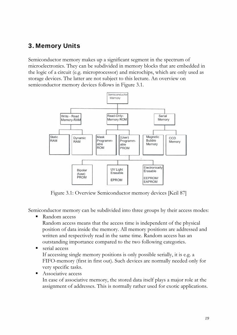
Semiconductor memory makes up a significant segment in the spectrum of microelectronics. They can be subdivided in memory blocks that are embedded in the logic of a circuit (e.g. microprocessor) and microchips, which are only used as storage devices. The latter are not subject to this lecture. An overview on semiconductor memory devices follows in Figure 3.1.
Figure 3.1: Overview Semiconductor memory devices [Keil 87]
Semiconductor memory can be subdivided into three groups by their access modes:
Random access Random access means that the access time is independent of the physical position of data inside the memory. All memory positions are addressed and written and respectively read in the same time. Random access has an outstanding importance compared to the two following categories.
serial access If accessing single memory positions is only possible serially, it is e.g. a FIFO-memory (first in first out). Such devices are normally needed only for very specific tasks.
Associative access In case of associative memory, the stored data itself plays a major role at the assignment of addresses. This is normally rather used for exotic applications.
20
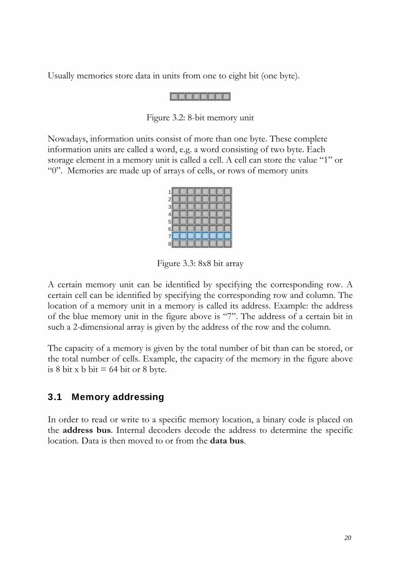
Usually memories store data in units from one to eight bit (one byte).
Figure 3.2: 8-bit memory unit Nowadays, information units consist of more than one byte. These complete information units are called a word, e.g. a word consisting of two byte. Each storage element in a memory unit is called a cell. A cell can store the value “1” or “0”. Memories are made up of arrays of cells, or rows of memory units
12345678
Figure 3.3: 8x8 bit array
A certain memory unit can be identified by specifying the corresponding row. A certain cell can be identified by specifying the corresponding row and column. The location of a memory unit in a memory is called its address. Example: the address of the blue memory unit in the figure above is “7”. The address of a certain bit in such a 2-dimensional array is given by the address of the row and the column. The capacity of a memory is given by the total number of bit than can be stored, or the total number of cells. Example, the capacity of the memory in the figure above is 8 bit x b bit = 64 bit or 8 byte.
3.1 Memory addressing
In order to read or write to a specific memory location, a binary code is placed on the address bus. Internal decoders decode the address to determine the specific location. Data is then moved to or from the data bus.
21
Rowaddressdecoder
Address bus Data bus
Write
Memory array
Read
Column address decoder
Figure 3.4: Basic Principle of Memory with Random Access
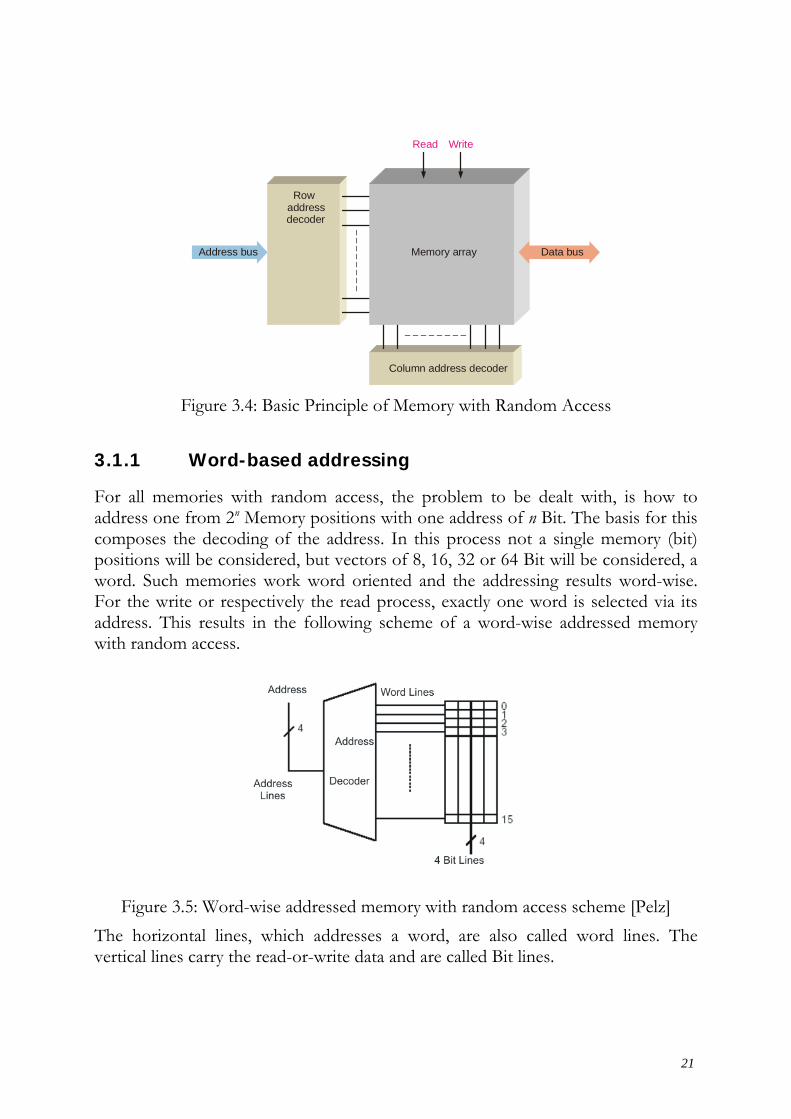
3.1.1 Word-based addressing
For all memories with random access, the problem to be dealt with, is how to address one from 2n Memory positions with one address of n Bit. The basis for this composes the decoding of the address. In this process not a single memory (bit) positions will be considered, but vectors of 8, 16, 32 or 64 Bit will be considered, a word. Such memories work word oriented and the addressing results word-wise. For the write or respectively the read process, exactly one word is selected via its address. This results in the following scheme of a word-wise addressed memory with random access.
Figure 3.5: Word-wise addressed memory with random access scheme [Pelz]
The horizontal lines, which addresses a word, are also called word lines. The vertical lines carry the read-or-write data and are called Bit lines.

22
Example: WRITE Operation
7
6
5
4
3
2
1
0
0 0 0 0 1 1 1 1
1 1 1 1 1 1 1 1
1 0 0 0 1 1 0 1
0 0 0 0 0 1 1 0
1 1 1 1 1 1 0 0
1 0 0 0 0 0 0 1
0
1
0
0
1
1
0
0
1
1
0
1
0
1
1
1
1 0 1
1
0 0 1
2
01 1 0 1
3
1. The address is placed on the address bus. 2. Data is placed on the data bus. 3. A write command is issued.
Figure 3.6: (Floyd)
Example: READ Operation
7
6
5
4
3
2
1
0
0 0 0 0 1 1 1 1
1 1 1 1 1 1 1 1
1 0 0 0 1 1 0 1
0 0 0 0 0 1 1 0
1 1 0 0 0 0 0 1
1 0 0 0 0 0 0 1
0
1
0
0
1
1
0
0
1
1
0
1
0
1
1
1
0 1 1
1
0 0 0
3
11 0 0 1
2
1. The address is placed on the address bus. 2. A read command is issued. 3. A copy of the data is placed in the data bus and shifted into the data register.
Figure 3.7: (Floyd)

23
3.1.2 Bit-wise addressing
There exists also the possibility to store more than one data word in single a memory word. When writing or reading, a complete memory word will however be selected first. In a further selection process the chosen data word is then identified. The memory possesses a second decoder for this; the column decoder; see Figure 3.8.
Figure 3.8: Bit-wise addressed memory with random access scheme [Pelz]
Should the memory possess m rows each consisting of n cells (columns), then a number of R data words of length N can be stored per row, whereby:
R=(n/N) The number of required address bits r for the column decoder can be determined from:
r = ld R The address for the row decoder can be reduced by r positions in this way.
3.2 RAMs and ROMs
Random access memory (RAM) and Read only memory (ROM) are the two major categories of semiconductor memories. Random access means that the access time is independent of the physical position of data inside the memory, an arbitrary data word can be read or stored at any point in time. All memory positions are addressed and written and respectively read in the same time. RAM is for temporary data storage that loses the stored data when the power is turned off. RAMs are volatile memories.
24
Read only means the data can be read only from a ROM, there is no write operation. In contrast to RAM the memory is stored permanently (or semi permanently). Like the RAM the ROM is a random access memory.
3.2.1 Random Access Memories (RAMs)
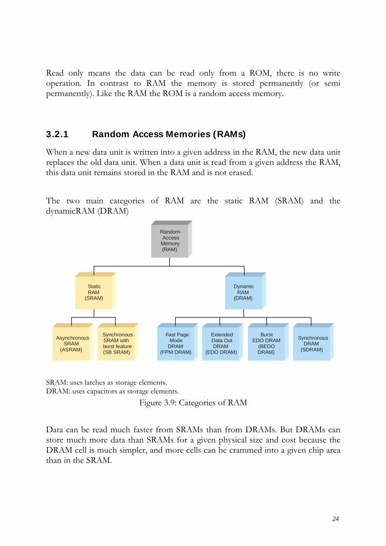
When a new data unit is written into a given address in the RAM, the new data unit replaces the old data unit. When a data unit is read from a given address the RAM, this data unit remains stored in the RAM and is not erased. The two main categories of RAM are the static RAM (SRAM) and the dynamicRAM (DRAM)
StaticRAM
(SRAM)
DynamicRAM
(DRAM)
AsynchronousSRAM
(ASRAM)
SynchronousSRAM withburst feature(SB SRAM)
ExtendedData OutDRAM
(EDO DRAM)
BurstEDO DRAM
(BEDODRAM)
Fast PageMode
DRAM(FPM DRAM)
SynchronousDRAM
(SDRAM)
Random-Access
Memory(RAM)
SRAM: uses latches as storage elements. DRAM: uses capacitors as storage elements.
Figure 3.9: Categories of RAM
Data can be read much faster from SRAMs than from DRAMs. But DRAMs can store much more data than SRAMs for a given physical size and cost because the DRAM cell is much simpler, and more cells can be crammed into a given chip area than in the SRAM.
25
3.2.1.1 Static RAMs (SRAM)
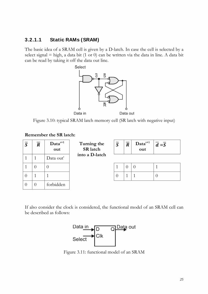
The basic idea of a SRAM cell is given by a D-latch. In case the cell is selected by a select signal = high, a data bit (1 or 0) can be written via the data in line. A data bit can be read by taking it off the data out line.
Figure 3.10: typical SRAM latch memory cell (SR latch with negative input)
Remember the SR latch:
Datat+1 out
Turning the SR latch
into a D-latch
Datat+1 out
=
1 1 Data outt
1 0 0 1 0 0 1
0 1 1 0 1 1 0
0 0 forbidden
If also consider the clock is considered, the functional model of an SRAM cell can be described as follows:
Figure 3.11: functional model of an SRAM

26
Basic static memory cell array
A SRAM cell array now uses the for every cell the above described latch memory cell. In the following an example for a n x 4 array is given
Row Select 1
Row Select 2
Row Select n
Row Select 0
Memory cell
Data Input/OutputBuffers and Control
Data I/OBit 0
Data I/OBit 1
Data I/OBit 2
Data I/OBit 3
Figure 3.12: Floyd
The cells in a row all share the same Row Select Line. Each set of Data In and Data Out lines is connected to each cell in a given column. To write a data unit into a given row of cells in the memory array, the ROW Select Line is taken to its active state and four data bit are placed on the Data I/O lines. Finally an additional write line in the control unit has to be set to its active state, which causes the data bit to be stored in the selected cells. To read a data unit, the Read Line has to be set to its active state, which causes that the stored data bit appear on the Data I/O lines. An easier representation of the above shown structure is given by a so-called logic diagram of an SRAM Tristate buffers allow the data lines to act as either input lines or output lines. Therefore an additional output enable signal is needed. The signal for chip select, output enable and write enable are to be generated by a control unit, e.g. in a computer by the CPU.

27
Figure 3.13: 256 x 4 RAM
READ Cycle
To read data from the memory, a valid address code has to be applied to the address lines for a specified time interval called the read cycle time tRC., beginning at t0. After allowing some time for the address signal to stabilize, the Chip Select and Output Enable signals go low. The RAM responds by placing the data onto the data output line at t1.The time t1 – t0 is the time between the application of a new address and the appearance of valid output data and is called the RAMs access time tAQ. The random access time tAQ. The timing parameters tEQ (chip enable access time) and tGQ (output enable access time) indicate the time it takes for the RAM output to go from Hi-Z (high impedance state) to a valid data level once the chip is selected and the output is enabled. At time t2 the chip select signal and the output enable signal returned HIGH, and the RAMs output returns to its Hi-Z state after a time interval tOD. Thus, the RAM data will be available between t1 and t3, and it can be taken at any point in time during this interval. The complete read cycle extends from t0 to t2.

28
Figure 3.14: RAM’s Read Cycle
WRITE Cycle
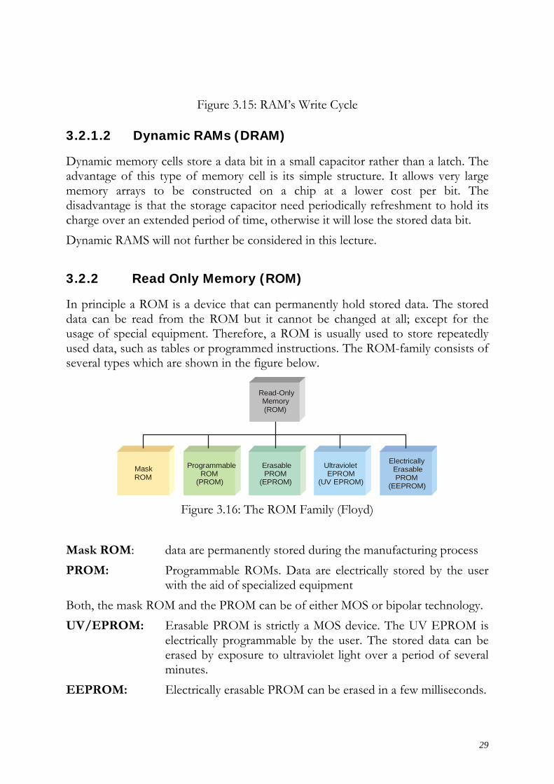
To write data to the memory, a valid address code has to be applied to the address lines for a specified time interval called the write cycle time tWC., beginning at t0. After allowing some time for the address signal to stabilize, the Chip Select and Write Enable signals go low. This time is called the address setup time tS(A). The time that the Write Enable signal must be low is the write pulse width and is called the write time interval tW. During the write time interval, at time t1 valid data applies on the input lines to be written to the memory. The data must be held at the RAMs input for at least a time interval tWD prior to, and for at least a time interval th(D) after, the deactivation of the write enable and chip select at t2. If any of these time requirements are not met, the write operation will not take place reliably. During each write cycle, one unit of data is written to the RAM.
29
Figure 3.15: RAM’s Write Cycle
3.2.1.2 Dynamic RAMs (DRAM)
Dynamic memory cells store a data bit in a small capacitor rather than a latch. The advantage of this type of memory cell is its simple structure. It allows very large memory arrays to be constructed on a chip at a lower cost per bit. The disadvantage is that the storage capacitor need periodically refreshment to hold its charge over an extended period of time, otherwise it will lose the stored data bit. Dynamic RAMS will not further be considered in this lecture.
3.2.2 Read Only Memory (ROM)
In principle a ROM is a device that can permanently hold stored data. The stored data can be read from the ROM but it cannot be changed at all; except for the usage of special equipment. Therefore, a ROM is usually used to store repeatedly used data, such as tables or programmed instructions. The ROM-family consists of several types which are shown in the figure below.
Read-OnlyMemory(ROM)
ElectricallyErasablePROM
(EEPROM)
MaskROM
ErasablePROM
(EPROM)
UltravioletEPROM
(UV EPROM)
ProgrammableROM
(PROM)
Figure 3.16: The ROM Family (Floyd) Mask ROM: data are permanently stored during the manufacturing process PROM: Programmable ROMs. Data are electrically stored by the user
with the aid of specialized equipment Both, the mask ROM and the PROM can be of either MOS or bipolar technology. UV/EPROM: Erasable PROM is strictly a MOS device. The UV EPROM is
electrically programmable by the user. The stored data can be erased by exposure to ultraviolet light over a period of several minutes.
EEPROM: Electrically erasable PROM can be erased in a few milliseconds.
30
In this chapter the Mask PROM will be introduced. The PROM will be discussed in detail in the next chapter
3.2.2.1 The Mask ROM
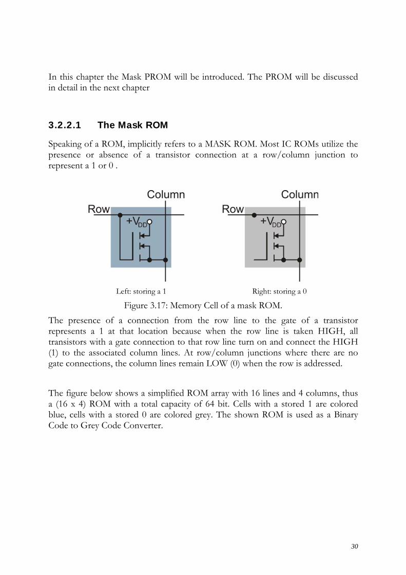
Speaking of a ROM, implicitly refers to a MASK ROM. Most IC ROMs utilize the presence or absence of a transistor connection at a row/column junction to represent a 1 or 0 .
Left: storing a 1 Right: storing a 0
Figure 3.17: Memory Cell of a mask ROM. The presence of a connection from the row line to the gate of a transistor represents a 1 at that location because when the row line is taken HIGH, all transistors with a gate connection to that row line turn on and connect the HIGH (1) to the associated column lines. At row/column junctions where there are no gate connections, the column lines remain LOW (0) when the row is addressed. The figure below shows a simplified ROM array with 16 lines and 4 columns, thus a (16 x 4) ROM with a total capacity of 64 bit. Cells with a stored 1 are colored blue, cells with a stored 0 are colored grey. The shown ROM is used as a Binary Code to Grey Code Converter.

31
Figure 3.18: (16x4) ROM as Binary Code ->Gray Code Converter
Most IC ROM’s have a more complex internal organization than the above described example. In the following the logic symbol of a ROM is given.

When bits app ROM
ROM address
any one opear on th
Access T
has an acs code on
Figure of 256 binahe outputs
Time
ccess timethe input l
3.19: A (2ary codes if the chip
ta, whichlines until
Figure 3.2
56 x 4) RO(8 bit) is ap enable in
h is the tithe appea
20: timing
OM Logic applied to nputs are L
ime from rance of v
diagramm
symbol the addres
LOW.
the applivalid outpu
m
ss lines, fo
cation of ut data.
32
our data
a valid

33
4. Programmable Logic Devices
4.1 General structure
Programmable logic devices (PLD) are Semi-Custom-ICs of low complexity with an AND- and an OR- Matrix for programming by the user or the manufacturer. Components with higher complexity and a matrix architecture of simple function blocks are described as Field Programmable Gate Array (FPGA). Figure 4.1 illustrates the general structure of all PLD. In it the following elements are recognisable :
• a programmable AND/OR - Matrix, • the programmable feedback, • an Input block, • an Output block.
figure 4.1: General PLD-Structure [Auer 1994]
The heart of all PLD ‘s is their programmable AND/OR matrix. The remaining elements must not necessarily be realised by all PLD ‘s. Within the programmable matrix, the outputs of logic AND-Gates lead to a matrix of logic OR-Gates as in figure 4.2
figure: 4.2: The structure of programmable AND/OR-matrices [Auer 1994]

34
The differentiation of the PLD-types illustrated in fig. 4.3 is based • on programming possibilities of the AND- and OR-matrices; • the way of how the programming takes place, either by
o the user (also called field programmable) or o the manufacturer (factory programmed).
The following components belong, among others to the group of PLD-IC : PROM: Programmable Read Only Memory contains a fixed AND-matrix. In
this fixed matrix, the addressing of the individual memory cells is realized. Only the OR-matrix is programmable by the customer. Data or logic functions, respectively will be stored in the OR-matrix. The well known EPROM-memory also belongs to this group which has the addressing of the memory cells in an AND-matrix as being fixed after being programmed by the manufacturer.
FPLA: Field Programmable Logic Array components consists of a customer programmable AND- and OR-matrix. The component increases not only the flexibility during the design but also the level of exploitation of the structure.
PAL: Programmable Array Logic components contain a fixed OR-matrix. Only the AND-matrix is electrically programmable by the customer. PAL is a registered trade mark of the company Monolithic Memories Inc. United States of America. HAL- Components (Hardware Array Logic) are the manufacturer programmed version of a PAL. The AND as well as the OR-matrix are to be seen by the user as being given and fixed.
GAL- Components (Generic Array Logic ) structurally similar to the PAL-components. In this we are dealing with electrically erasable and electrically programmable logic-arrays. GAL is a trade mark of Lattice Semiconductors. EPLD – Components (Erasable Programmable Logic Device) also structurally similar to the PAL-Components. Instead of "fuse programming" used for "Standard"-PAL, Floating-Gate-Technology is used for EPLD- Components: the component can be erased by UV-light and thereby be available for new programming. Possible programming errors can be overcome in this way without losing any of the components.

35
figure 4.3: Summary of the PLD-Variations
In the summary of variations illustrated above FPLA are given as representatives of components built upon the basis of the Integrated Fuse Logic. In this case we are dealing with a notation of the Company Valvo. The programming takes place via the separation of the melting paths (Fuse Link) on the crossing lines of the AND/OR-matrices. Due to the complexity we will differentiate a total of four types: FPLA: freely programmable Logic Array; see above. FPGA: Field Programmable Gate Array (freely programmable Gate Array) with
programmable AND-matrix; FPLS: Field Programmable Logic Sequencer (freely programmable logic
sequencer) with register functions at the output of the programmable matrices;
FPRP: freely programmable ROM-Patch with a fixed programmed AND-matrix as address decoder and programmable OR-matrix as data memory .
Advantages of PLD’s
• Reduced complexity of circuit boards o Lower power requirements o Less board space o Simpler testing procedures
• Reduced complexity of circuit boards
• Higher reliability
• Design flexibility
36
4.2 Construction of the AND/OR-Matrix
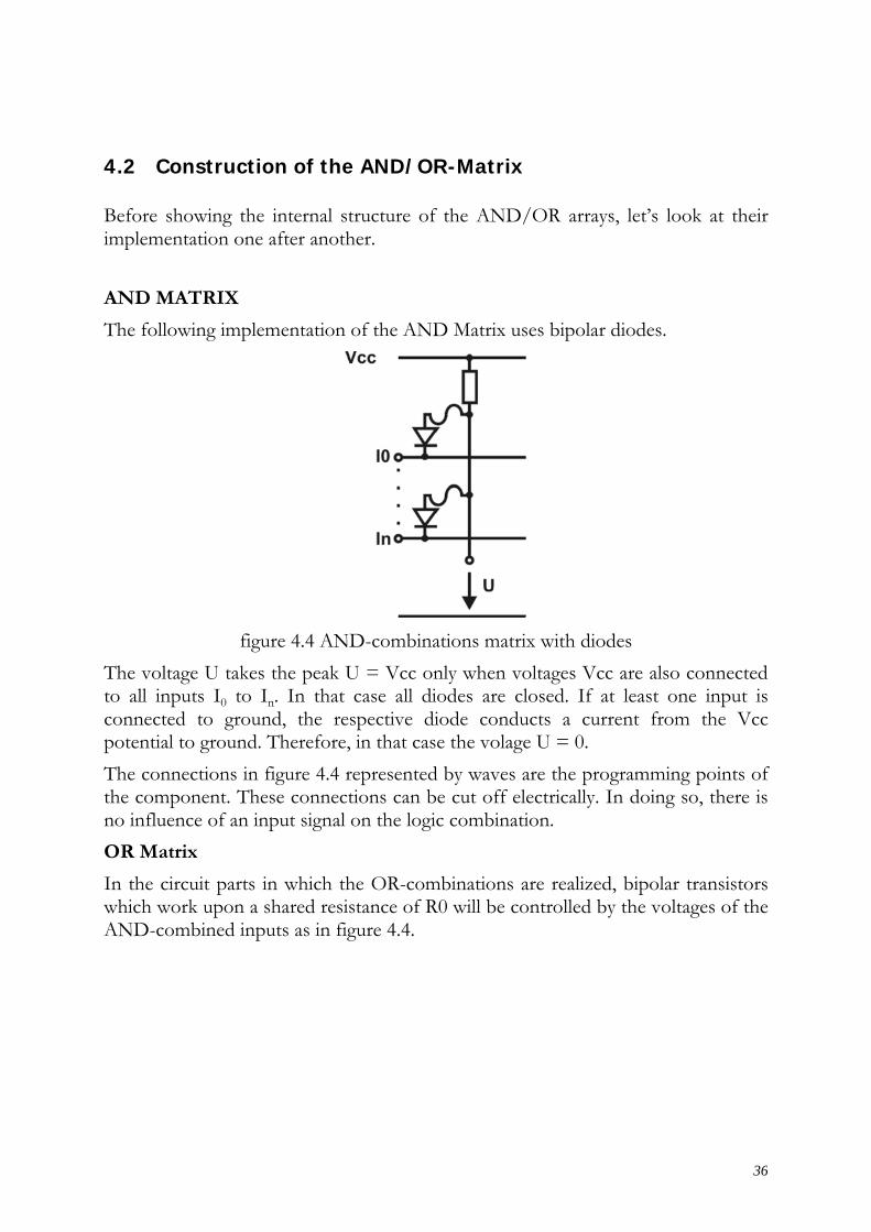
Before showing the internal structure of the AND/OR arrays, let’s look at their implementation one after another. AND MATRIX
The following implementation of the AND Matrix uses bipolar diodes.
figure 4.4 AND-combinations matrix with diodes
The voltage U takes the peak U = Vcc only when voltages Vcc are also connected to all inputs I0 to In. In that case all diodes are closed. If at least one input is connected to ground, the respective diode conducts a current from the Vcc potential to ground. Therefore, in that case the volage U = 0. The connections in figure 4.4 represented by waves are the programming points of the component. These connections can be cut off electrically. In doing so, there is no influence of an input signal on the logic combination. OR Matrix
In the circuit parts in which the OR-combinations are realized, bipolar transistors which work upon a shared resistance of R0 will be controlled by the voltages of the AND-combined inputs as in figure 4.4.

37
Figure4.5: Circuit part for the realization of the OR-combinations [Auer 1994]
The voltage on the R0 resistor will have the peak UR0 = Vcc when at least one transistor is active. There also exist circuit variations with multi-emitter-transistors with an active L-peak. Combination of AND/OR Matrix
The structure of the AND/OR-matrices of the PLD-components can be illustrated in such a way that the principal construction is immediately recognisable. Three AND/OR-matrices – each of them realized in bipolar technology- are combined to each other. The general structure is illustrated once again in figure 4.6

38
Figure 4.6: general construction of the AND/ OR- Matrices [Auer 1994]
Figure 4.7 shows an example of a programmed device. Here exactly one of the three (green) word lines is addressed via a 1 from m decoder and the stored data are delivered through the (red) bit-lines.

39
Figure 4.7: Example of a programmed device
In the circuit illustrated above, the following values will be delivered upon choosing one of the rows.
x y z I0 I 0 I I1 0 I I I2 0 0 0
Table 4.1
4.3 Types of Illustrations
It is hardly possible to illustrate the full electronic circuit of the matrix. For the multiple AND-and OR-combinations built in within the matrix, simplified illustrations, are brought in.

40
An initial agreement for the simplification is concerned with the illustration of the programming points, which can be destroyed whilst programming. These connections are denoted by waves in complete circuits; see figure 4.8a. Alternative illustrations or simplifications respectively, illustrate this connection as a point, figure 4.8b or as a star, figure 4.8c. Two lines crossing each other without a point or star respectively represent “not connected”.
4.8a 4.8b 4.8c
Figure 4.8: Types of illustrations of the Programming Points The detailed electrical connection in the crossing points of the matrices is graphically illustrated once again in figure 4.9 here the symbolical illustration is contrasted to the technical realization.
left: connected right: not connected
figure 4.9: Technical Realization of the Connections A second agreement concerned with the multiple combinations of the n-inputs to the AND or OR-Gates respectively. Figure 4.10a shows for this the electronic illustration and figure 4.10b a simplified illustration whereby the logic function with the multiple inputs and the separable connections is highlighted. In figure 4.10c the illustration is further simplified, whereby only a horizontal line to the Gate is illustrated and the input signals cross this horizontal line as vertical lines. A point on which the lines cross each other implies that there exists an electrical connection
41
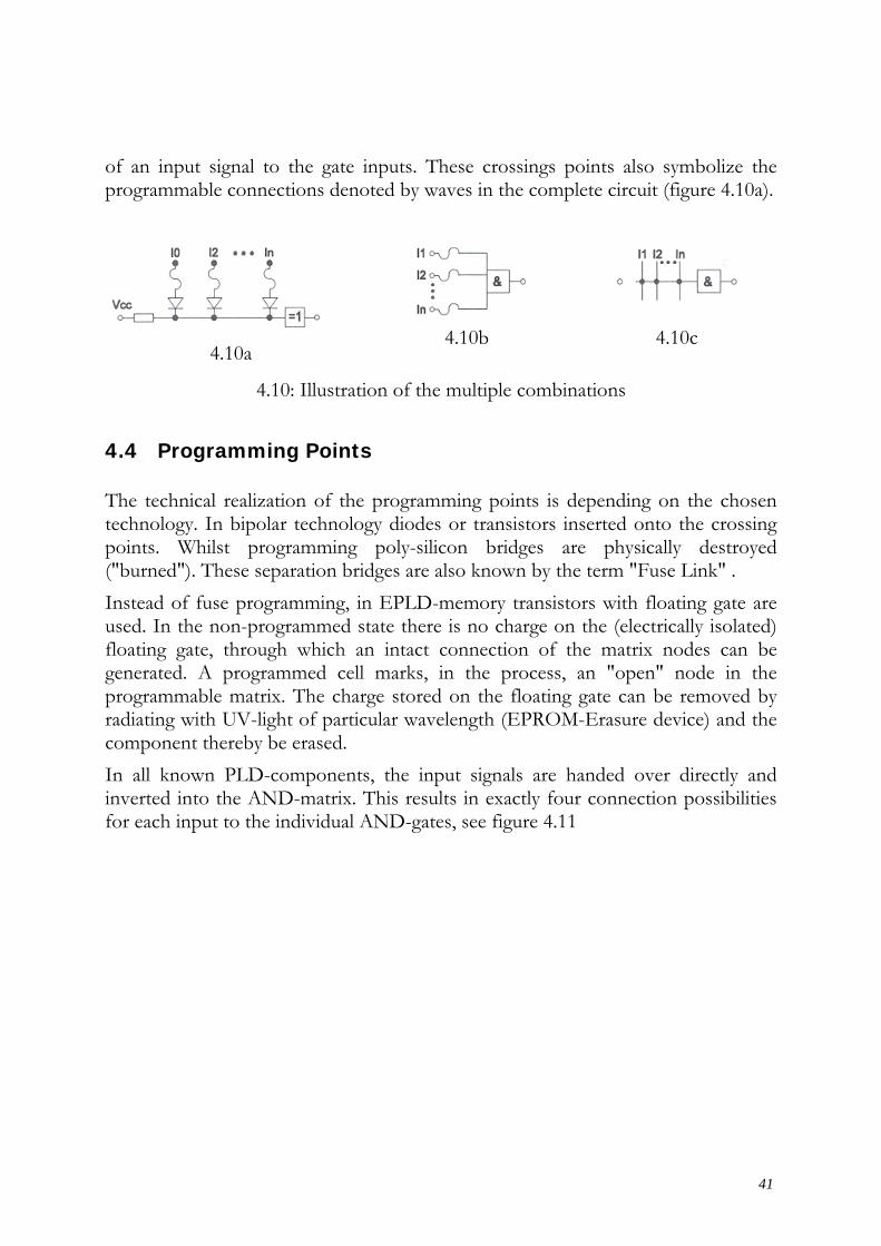
of an input signal to the gate inputs. These crossings points also symbolize the programmable connections denoted by waves in the complete circuit (figure 4.10a).
4.10a
4.10b
4.10c
4.10: Illustration of the multiple combinations
4.4 Programming Points
The technical realization of the programming points is depending on the chosen technology. In bipolar technology diodes or transistors inserted onto the crossing points. Whilst programming poly-silicon bridges are physically destroyed ("burned"). These separation bridges are also known by the term "Fuse Link" . Instead of fuse programming, in EPLD-memory transistors with floating gate are used. In the non-programmed state there is no charge on the (electrically isolated) floating gate, through which an intact connection of the matrix nodes can be generated. A programmed cell marks, in the process, an "open" node in the programmable matrix. The charge stored on the floating gate can be removed by radiating with UV-light of particular wavelength (EPROM-Erasure device) and the component thereby be erased. In all known PLD-components, the input signals are handed over directly and inverted into the AND-matrix. This results in exactly four connection possibilities for each input to the individual AND-gates, see figure 4.11

42
figure 4.11: possible connections of the inputs to the AND-Gates [Auer 1994]
An AND-Gate is constantly set to 0-Peak, when the connections shown in fig. 4.11a remain non-programmed (intact). The influence of a corresponding input on the AND-Gates is ruled out by the separation of both connections. Should one of the two connections remain available as in fig. 4.11c or fig. 4.11d respectively, then the input is effectively direct i.e. negated at the AND-Gate. Finally, figure 4.12 shows some examples
a.) programmed AND-matrix with
O1= 321 III ⋅⋅ O3= 31 II ⋅
b.) PLD

43
O2= 21 II ⋅
Figure. 4.12: Example of a PLDs
4.5 PLD Structures
In correspondence to the demands of circuit development the following PLD-structures are offered :
• Combinational PLD-structure, • Combinational PLID-structure with feedback, • PLD with registered outputs and feedback , • PLD with programmable output polarity, • Exclusive-OR-Function combined with registered outputs, • Programmable registered inputs, • PLD with product-term-shading, • PLD with asynchronous registered outputs, • GAL with programmable macro cells for signal outputs.
From the multitude of structure a few interesting architectures will be closely illustrated in the following.
4.5.1 Combinatorial PLD
Characteristic of the combinational PLD is the AND/OR-matrix-structure where the feedback branch and the storage possibilities on the in- and outputs are missing. In this version programmable AND-matrix is available. This structure is illustrated in figure 4.13.
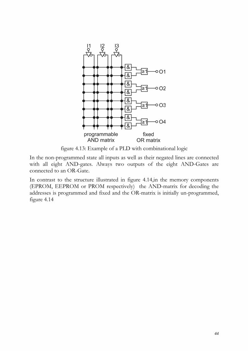
44
figure 4.13: Example of a PLD with combinational logic
In the non-programmed state all inputs as well as their negated lines are connected with all eight AND-gates. Always two outputs of the eight AND-Gates are connected to an OR-Gate. In contrast to the structure illustrated in figure 4.14,in the memory components (EPROM, EEPROM or PROM respectively) the AND-matrix for decoding the addresses is programmed and fixed and the OR-matrix is initially un-programmed, figure 4.14

45
figure 4.14: Exemplary Structure of a PROM- or EPROM memory respectively
In the PROM-memory connections in the OR-matrix will be burned out whilst the programming takes place, and so the component is not reprogrammable. In case of EPROM, all connections in the OR-matrix are reactivated with UV-Light or electrically in the EEPROM respectively and these connections will be rescinded when programming. An example of a combinational PAL-Structure is shown in figure 4.15.
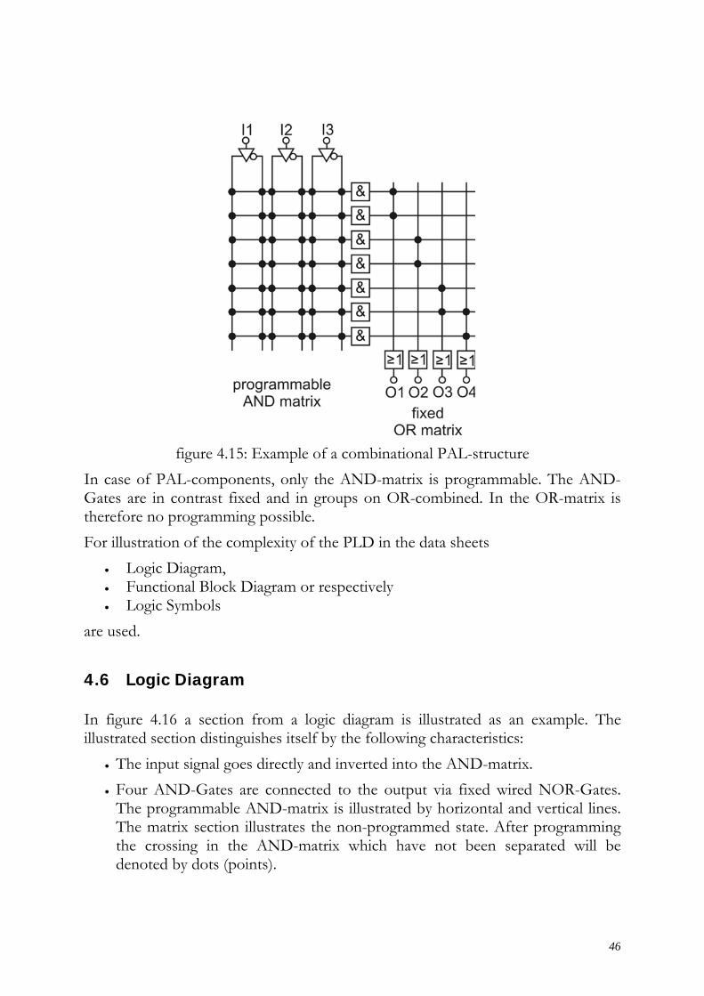
46
figure 4.15: Example of a combinational PAL-structure
In case of PAL-components, only the AND-matrix is programmable. The AND-Gates are in contrast fixed and in groups on OR-combined. In the OR-matrix is therefore no programming possible. For illustration of the complexity of the PLD in the data sheets
• Logic Diagram, • Functional Block Diagram or respectively • Logic Symbols
are used.
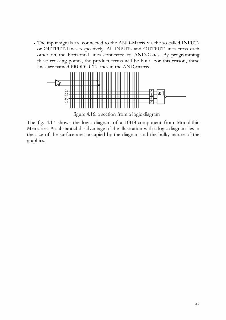
4.6 Logic Diagram
In figure 4.16 a section from a logic diagram is illustrated as an example. The illustrated section distinguishes itself by the following characteristics:
• The input signal goes directly and inverted into the AND-matrix. • Four AND-Gates are connected to the output via fixed wired NOR-Gates.
The programmable AND-matrix is illustrated by horizontal and vertical lines. The matrix section illustrates the non-programmed state. After programming the crossing in the AND-matrix which have not been separated will be denoted by dots (points).
47
• The input signals are connected to the AND-Matrix via the so called INPUT- or OUTPUT-Lines respectively. All INPUT- and OUTPUT lines cross each other on the horizontal lines connected to AND-Gates. By programming these crossing points, the product terms will be built. For this reason, these lines are named PRODUCT-Lines in the AND-matrix.
figure 4.16: a section from a logic diagram
The fig. 4.17 shows the logic diagram of a 10H8-component from Monolithic Memories. A substantial disadvantage of the illustration with a logic diagram lies in the size of the surface area occupied by the diagram and the bulky nature of the graphics.
48
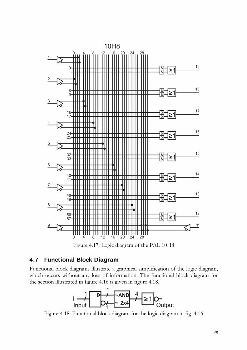
Figure 4.17: Logic diagram of the PAL 10H8
4.7 Functional Block Diagram Functional block diagrams illustrate a graphical simplification of the logic diagram, which occurs without any loss of information. The functional block diagram for the section illustrated in figure 4.16 is given in figure 4.18.
Figure 4.18: Functional block diagram for the logic diagram in fig. 4.16
49
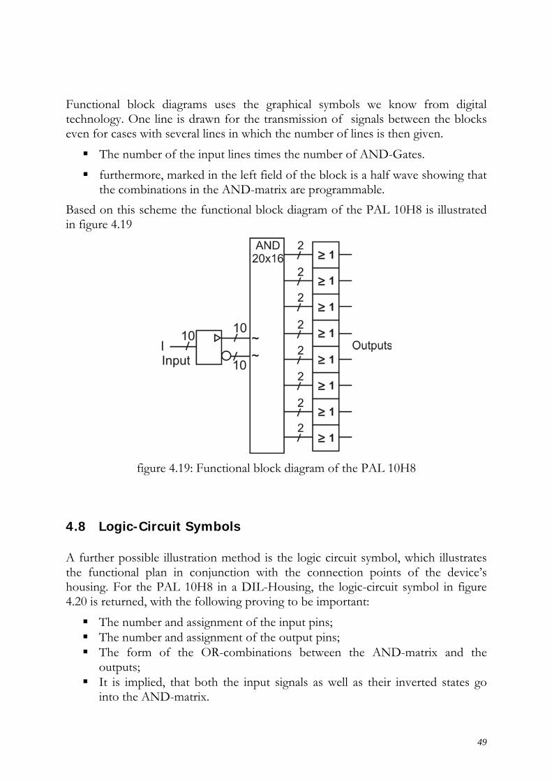
Functional block diagrams uses the graphical symbols we know from digital technology. One line is drawn for the transmission of signals between the blocks even for cases with several lines in which the number of lines is then given.
The number of the input lines times the number of AND-Gates. furthermore, marked in the left field of the block is a half wave showing that
the combinations in the AND-matrix are programmable. Based on this scheme the functional block diagram of the PAL 10H8 is illustrated in figure 4.19
figure 4.19: Functional block diagram of the PAL 10H8
4.8 Logic-Circuit Symbols
A further possible illustration method is the logic circuit symbol, which illustrates the functional plan in conjunction with the connection points of the device’s housing. For the PAL 10H8 in a DIL-Housing, the logic-circuit symbol in figure 4.20 is returned, with the following proving to be important:
The number and assignment of the input pins; The number and assignment of the output pins; The form of the OR-combinations between the AND-matrix and the
outputs; It is implied, that both the input signals as well as their inverted states go
into the AND-matrix.

50
figure 4.20: Logic circuit symbol of the combinational PAL 10H8
4.9 The Programming of the PLD
For Circuit development with PLD-components it is important when accommodating the logic function in the IC to know which functions are realisable at all. Here principally four elementary programmable signal paths in the AND-matrix of PLD-components, illustrated in figure 4.21, are with combinational logic possible.
figure 4.21: Programmable elements of the AND matrix and their logic-functions
The connections that have not been cut off will be denoted by a dot on the lines of the matrix crossing. Should both connections from the input lines to the product lines of an AND-Gate remain intact (figure 4.21a), the output of the AND-Gate is constantly programmed to L. Should only one of the two connections remain, as in
51
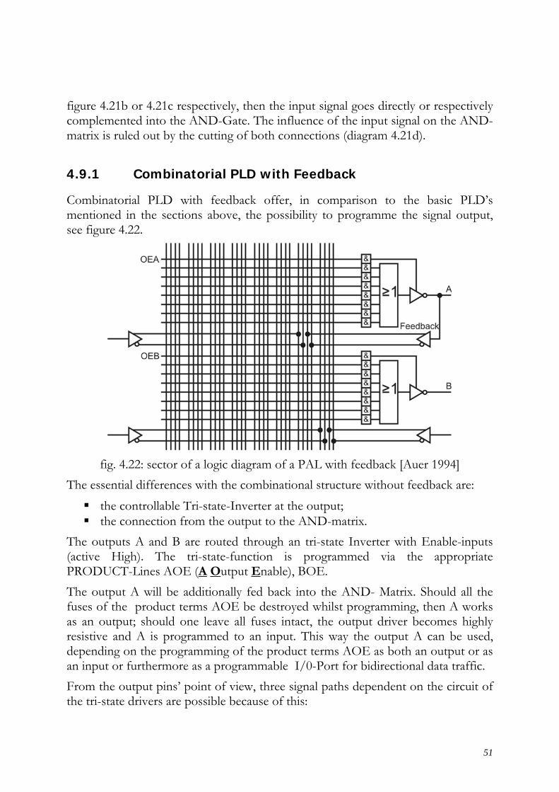
figure 4.21b or 4.21c respectively, then the input signal goes directly or respectively complemented into the AND-Gate. The influence of the input signal on the AND-matrix is ruled out by the cutting of both connections (diagram 4.21d).
4.9.1 Combinatorial PLD with Feedback
Combinatorial PLD with feedback offer, in comparison to the basic PLD’s mentioned in the sections above, the possibility to programme the signal output, see figure 4.22.
fig. 4.22: sector of a logic diagram of a PAL with feedback [Auer 1994]
The essential differences with the combinational structure without feedback are: the controllable Tri-state-Inverter at the output; the connection from the output to the AND-matrix.
The outputs A and B are routed through an tri-state Inverter with Enable-inputs (active High). The tri-state-function is programmed via the appropriate PRODUCT-Lines AOE (A Output Enable), BOE. The output A will be additionally fed back into the AND- Matrix. Should all the fuses of the product terms AOE be destroyed whilst programming, then A works as an output; should one leave all fuses intact, the output driver becomes highly resistive and A is programmed to an input. This way the output A can be used, depending on the programming of the product terms AOE as both an output or as an input or furthermore as a programmable I/0-Port for bidirectional data traffic. From the output pins’ point of view, three signal paths dependent on the circuit of the tri-state drivers are possible because of this:

52
Tri-state-driver is continuously active: the pin connection points work exclusively as outputs with a feedback of the signal in the AND-Matrix (internal feedback); Should all the fuses in the product term AOE be cut off, then the associated AND- Gate will always lie on the H-level (compare also figure 5.20), and it’s output therefore frees the output driver. The connection point A will accordingly be continuously operated as an output. The signal that appears at the output via the internal feedback, inverted or not, again fed back into the AND-matrix.
Tri-state-driver is continuously in a highly impedance state: the pins work exclusively as an input; Should all programmable fuses on the PRODUCT-Line AOE remain unchanged, or both fuses remain intact for any input on this line respectively, then the respective AND-Gate will always be inactive. The output driver is switched to a high impedance state and interrupts the AND-matrix connection to the output pin. This way pin A can only be operated as an input.
Tri-state driver changes it’s function: the pin output will alternatively be operated as an input or output respectively. The output driver is controllable as an in-/output via a programmable logic combination on the PRODUCT-Line AOE . This mode of operation of a pin is suitable for bidirectional data traffic.
4.9.2 Special Features of Feedback
Feedback on the same Product Line A feedback from the output onto the same product line can be found in figure 4.23a and b. In figure 4.23a a feedback to the same product line is programmed. When all further programmed connections on the observed product line are H-level, then the output will oscillate between H and L via the feedback taking into consideration the signal propagation time. The frequency of the oscillations is dependent on the propagation time of the participating gates and cannot be influenced outside the IC . Flow diagram 4.23a: The value C lies at the output of the AND-Gate. This appears inverted according to the propagation time of the inverter at the output A and will be with the propagation time of the inverter in the feedback path fed back into the AND-matrix. The logic value L (respectively C ) then lies at the intact crossing

53
point or at the input of the AND-Gate respectively), while the value C still lies at the output. The output of the gate also changes it’s value in accordance with the propagation time of the gate.
figure 4.23: Feedback paths
Feedback onto another Product Line The signal feedback from the output to another product line in the AND-matrix is denoted in figure 4.23c . In both cases the output A1 generates a signal back into the AND-matrix and is forwarded via the product line to the output A2. Should a product line not transmit a signal which has been fed back (figure 4.23d) then the transition path for the feedback becomes transparent. Example Data should be transmitted bidirectional via pin 14 of the PAL 16L8, and when E1=H (Pin6) and E2=L (Pin7) and E3=H (Pin8), pin 14 should work as an output. Otherwise P14 works as an input. The signal paths programmed for this are denoted in bold in the logic diagram of the PAL 16L8 (figure 4.24).
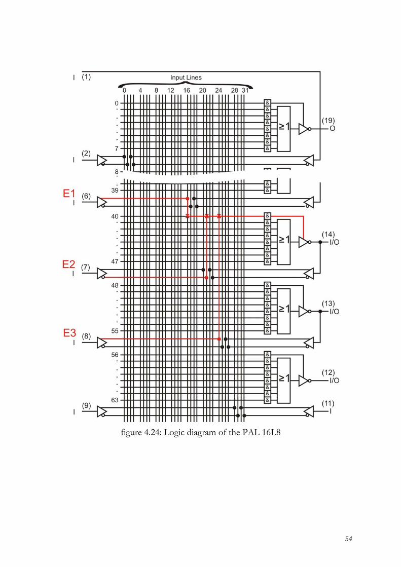
54
figure 4.24: Logic diagram of the PAL 16L8
55
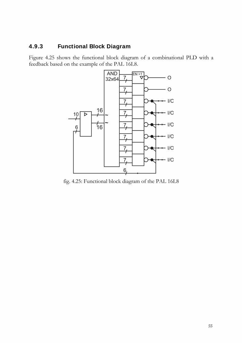
4.9.3 Functional Block Diagram
Figure 4.25 shows the functional block diagram of a combinational PLD with a feedback based on the example of the PAL 16L8.
fig. 4.25: Functional block diagram of the PAL 16L8

56
5. Algorithmic Minimization Approaches
The task of logic design is the conversion of the behavior of combinatorial and sequential circuits to structural descriptions, e.g. on the gate-layer. Often, the starting point is a description by means of truth-tables, Boolean equations or state transition tables, as used in the lectures of “Fundamentals of Computer Engineering 1”. This chapter gives in an intensively compact form, an overview of the prerequisite basic principles. The axioms, examples and procedures introduced in the following subchapters are without demanding completeness and should be accompanied by additional literature or by going through the content of the lecture „Fundamentals of Computer Engineering 1“ if necessary. Mainly this chapter aims at an extension of the spectrum of already known principles for minimization. Therefore the Quine/Mc Cluskey algorithm for minimization of complex combinatorial functions as well as the Moore Algorithm for state machine minimization will be introduced.
5.1 Minimization of combinational Functions
Complex logic expressions and therefore also technical realization via logic gates require often a minimization. For this, three procedures can be of usage:
1. Algebraic (mathematical) minimization by application of Boolean Algebra 2. Graphical minimization (Karnaugh-Veitch-(KV-)Map) 3. Algorithmic minimization (e.g. Quine-McCluskey algorithm)
for 1: Basic terms for algebraic minimization
Canonical forms Every switching expression can be written down in a canonical form. This is often useful during development. There are the two canonical forms: the disjunctive normal form (DNF) and conjunctive normal form (CNF). To understand these forms, we have to explain literals, minterms and maxterms first. Literals: A literal is either a variable or the complement of a variable. Minterm: A minterm is a logical sum (disjunction) of exactly n literals with no
repeated variables. With n variables we thus have 2n possible Minterms. Example (n=3):
57
CBA ⋅⋅ CBA ⋅⋅ CBA ⋅⋅ CBA ⋅⋅CBA ⋅⋅ CBA ⋅⋅ CBA ⋅⋅ CBA ⋅⋅
Maxterm: A Maxterm is a logical product (conjunction) of exactly n literals with no repeated variables. With n variables we thus have 2n possible Maxterms. Example (n=2):
BA + BA + BA + BA +
Sum-of-products (SOP)
The sum-of-products is a regular form consisting of a sum of m terms, where every term is a product:
CBCBABAfSOP ⋅+⋅⋅+⋅=
Product-of-sums (POS)
The product-of-sums is a regular form consisting of a product of m terms, where every term is a sum:
( ) ( ) ( )CBCBACAfPOS +⋅++⋅+=
Disjunctive Normal Form (DNF)
The DNF is a sum of products (SOP) consisting only of Minterms. Therefore every variable must appear exactly once in each product.
CBACBACBACBACBAfDNF ⋅⋅+⋅⋅+⋅⋅+⋅⋅+⋅⋅=
Conjunctive Normal Form (CNF)
The CNF is the product of sums (POS) only containing Maxterms. Therefore every variable must appear exactly once in each sum.
( ) ( ) ( )CNFf A B C A B C A B C= + + ⋅ + + ⋅ + +
De Morgan: It is true that: baba *=+ i.e. baba +=* Shannon extended this rule to n variables.
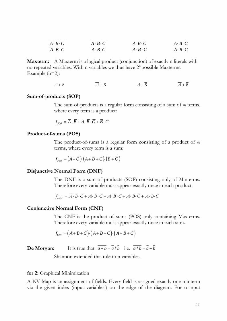
for 2: Graphical Minimization A KV-Map is an assignment of fields. Every field is assigned exactly one minterm via the given index (input variables!) on the edge of the diagram. For n input
58
variables 2n fields result in this way. The indexing must be in such a way that every field differs in only one variable with the one lying next to it. In the following some examples are given.
KV-Map with 3-Variables KV-Map with 4 Variables KV-Map with 5 Variables
Figure 5.1: Kv-Maps In a KV-Map: 1 field represents 1 minterm (n Variables) 2 fields lying next to each other represent n-1 variables 3 fields lying next to each other represent n-2 variables
M n fields represent the 1-Function (e.g. 1),,( =CBAf )
Minimization Procedure:
All fields, which represents a “1“-minterm of the function (VDNF), will be marked.
In this way as many as possible marked fields lying next to each other will be summarized in a way that they can be described by a minimum number of input variables (1,2,4,8...fields).
Several such resulting products will be OR-combined. Should a task allow for a minterm to be 0 or 1 ( don’t care), a field marked in
this way can be used, as if it were “1“.
59
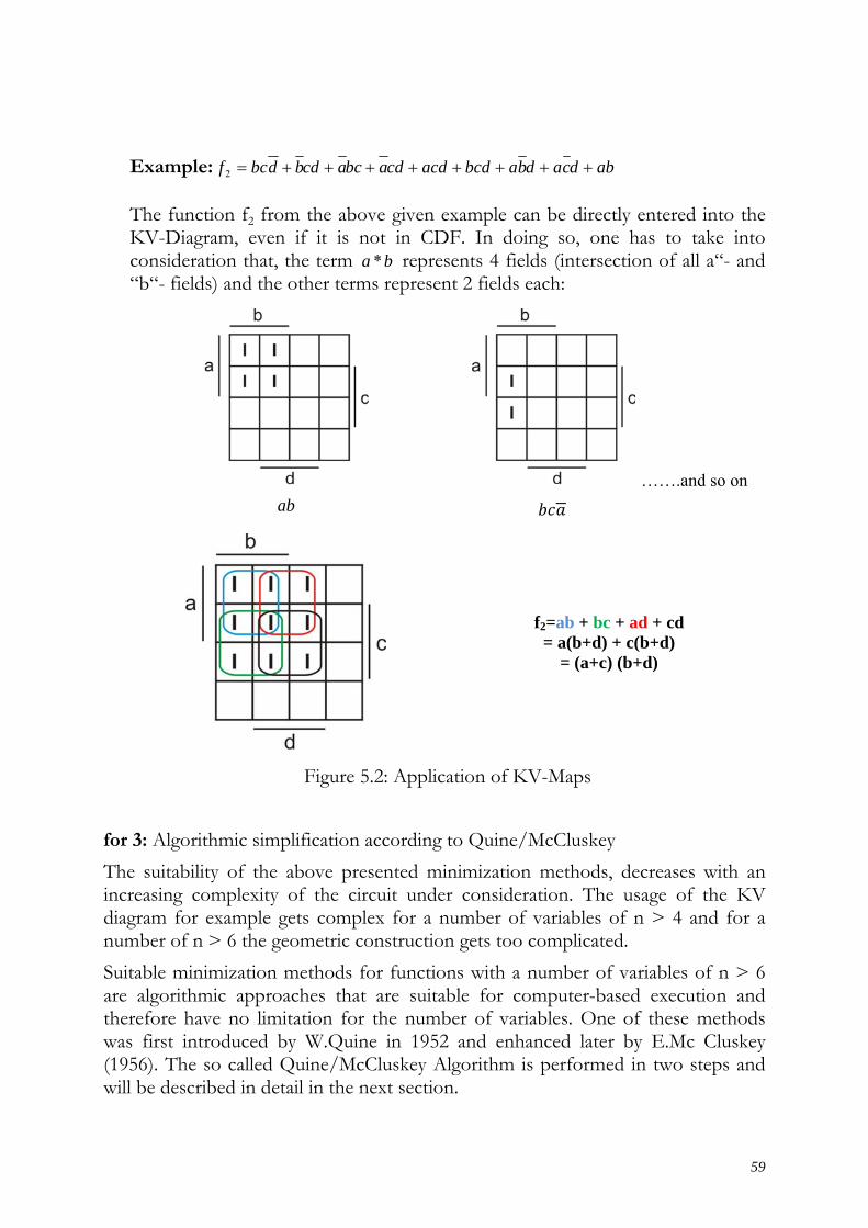
Example: abdcadbabcdacdcdabcacdbdbcf ++++++++=2 The function f2 from the above given example can be directly entered into the KV-Diagram, even if it is not in CDF. In doing so, one has to take into consideration that, the term ba * represents 4 fields (intersection of all a“- and “b“- fields) and the other terms represent 2 fields each:
ab
…….and so on
f2=ab + bc + ad + cd = a(b+d) + c(b+d)
= (a+c) (b+d)
Figure 5.2: Application of KV-Maps
for 3: Algorithmic simplification according to Quine/McCluskey The suitability of the above presented minimization methods, decreases with an increasing complexity of the circuit under consideration. The usage of the KV diagram for example gets complex for a number of variables of n > 4 and for a number of n > 6 the geometric construction gets too complicated. Suitable minimization methods for functions with a number of variables of n > 6 are algorithmic approaches that are suitable for computer-based execution and therefore have no limitation for the number of variables. One of these methods was first introduced by W.Quine in 1952 and enhanced later by E.Mc Cluskey (1956). The so called Quine/McCluskey Algorithm is performed in two steps and will be described in detail in the next section.
60
5.1.1 The Quine / McCluskey algorithm
The Quine / McCluskey algorithm is split-up into two major parts: 1. determination of the prime implicants of the given function 2. selection of a minimum set (number) of prime implicants that cover the given
function (and has the minimum cost). Given is a function f with a number of n variables and consisting of a number of i minterms mi and j don’t care terms dj.
0, 1, … . n i j
Without loss of generalization we will in the following consider only functions consisting of minterms only, like
0, 1, … . n i
1st Step: Determination of prime implicants
Definition: A term p of a logic function f is called prime term if it cannot be combined with another term of f that differs from p.
or: Prime term p of f is a subdomain of f and all variables are needed. The first task thus is to find pairs of terms that differ in only one variable, starting from the DNF. For that purpose the following scheme will be used consecutively. Successive procedure: (algorithmic description) 1.1 Determination of the DNF and a list of minterms 1.2 As far as possible: pairwise combination of (min)terms and set up of a
list of products
1.3 Repetition of 1.2 with an updated list after every repetition until:
1.4 no further minimization is possible any more.
Result on termination: Note all combined terms and all unused minterms. Together, these are the prime implicants of the function f, which now can be written as
0, 1, … . n k with pk = prime implicants and k= number of prime implicants

2nd Step: Determine the minimum number of prime implicants (minimum cover)
Successive procedure: (algorithmic description) 2.1 Construction of a prime-implicant chart
The prime implicant chart is a table in which the rows correspond to the prime implicants and the columns to the minterms. Each row (prime implicant) is marked with a “x”, if the minterm corresponding to that column is covered by the prime implicant.
2.2 Determination of essential prime implicants
Search for all columns with only one “x” (origin cross). In such cases the minterm mi is associated to exactly one prime implicant pj. Prime implicants fulfilling this condition are called essential prime implicants. All rows containing a prime implicant are called essential rows. All essential prime implicants have to be part of the solution.
2.3) Reduction of prime implicant chart
a.) Cancellation of all columns with x in essential row. b) Cancellation of arisen empty rows
Result so far: • Explicit minimization (no options and choices) • Determination of the essential prime implicants • Determination of a reduced matrix (by means of canceling columns and rows). Algorithm can terminate here! In general: not all minterms are covered by now. Therefore, selection of prime implicants which cover the remaining minterms is needed. 2.4) Search for identical rows
In case of identical rows: Choice of one row and cancelation of the remaining identical row(s).
2.5) Search for dominant rows
A row rx is covered by a row ry if the set of minterms covered by rx is a subset of the minterms covered by ry. Dominated rows can be cancelled out.
2.6) Search for dominant columns

62
Example
The Quine/Mc Cluskey algorithm will now be presented on the following example. Origin is the equation f1 in its DNF.
f A B C D ABCD ABCD ABCD ABCD ABCD ABCD1 ( , , , ) = + + + + +
1.1 Determination of the DNF and a list of minterms
Every term in f1 represents a minterm of the function f1. To every single of these minterms a weight can be assigned now, which gives the number of non-negated variables.
3
3
2
3
1
1
6
5
4
3
2
1
==
==
==
==
==
==
WeightDABCm
WeightDCABm
WeightDBCAm
WeightBCDAm
WeightDCBAm
WeightDCBAm
Now the following (minterm) table can be constructed, in which the minterms are organized in ascending weight. In doing so, all minterms are grouped in classes of weights. Weight Nr A B C D Minterm
1 1 0 0 0 I m1 2 0 0 I 0 m2 2 3 0 I I 0 m4 4 0 I I I m3 3 5 I I 0 I m5 6 I I I 0 m6
Table 5.1: minterm table
1.2 As far as possible: pairwise combination of (min)terms and set up of a list of products
The task of pairwise combination of minterms starts with combining minterms which differ in only one variable. This step is comparable to the combination of two neighboring fields in a KV-Map. In the Quine/McCluskey algorithm the search for these terms occurs by comparison of every minterm of weight g with all minterms in neighboring classes with weights g+1 and g-1. Differences in only one variable occur in such a way,

63
that in the minterm of weight g a certain variable is given in negated form and in the minterm of weight g+1 (or g-1) the same variable is given in non-negated form. Looking at table 5.1 we start with m1 and compare this with m4. It can be seen that these two minterms differ in more than one variable and therefore cannot be combined. In the next table m1 has to included in its original form; see first line in table 5.2. Compare m2 and m4: these two minterms differ only in the variable B. Therefore they can be combined. The result is given as the second row in table 5.2. Notice that the origin is marked in the left colums. In the same manner the following comparisons have to be conducted:
− m4 and m3 − m4 and m5 − m4 and m6
Finally, the resulting table can be given. origin A B C D
m1 0 0 0 I m2,m4 0 - I 0 m3,m4 0 I I - m5 I I 0 I m4,m6 - I I 0 Table 5.2
1.3 Repetition of 1.2 with an updated list after every repetition until:
The first step has to be repeated until no more combining is possible any more. At first the algorithm searches for terms marked with a “-“ at the same position and that differ in only one more variable. Such terms can be further combined and have to be marked in the resulting table with an additional “-“. At this stage, identical terms are possible. In this case one of them can be deleted. In comparison to the KV-map, here all neighboring 4-fields are combined. All rows that can be further combined have to be marked and can be left out from the production of the next table, but must be considered at the final step 1.4. In the next repetition all neighboring 2n fields are combined. If no more combining is possible, all non-marked, non-deleted rows give the prime terms of the function. In this example, the first minterm table is not combinable any further and thus directly gives the prime implicants of the function f1.

64
1.4 no further minimization is possible any more.
In case no further combinations are possible, every row of the resulting table gives a prime implicant origin A B C D Prime implicants m1 0 0 0 I p1 m2,m4 0 - I 0 p2 m3,m4 0 I I - p3 m5 I I 0 I p4 m4,m6 - I I 0 p5 Table 5.3
The function f1 therefore can now be written as
f p p p p p
ABCD ACD ABC ABCD BCD1 1 2 3 4 5= + + + +
= + + + +
With it, step 1 of the Quine/Mc Cluskey algorithm is finished.
2nd Step: Determine the minimum number of prime implicants (minimum cover)
2.1 Construction of a prime-implicant chart
The 2nd step starts with the construction of the prime-implicant chart. Table 5.4 gives the prime implicant chart of the function f1.
⇒ Minterm m1 m2 m3 m4 m5 m6
⇓ p1 x Prime- p2 x x
implicants p3 x x p4 x p5 x x Table 5.4 : prime-implicant chart of the function f1
It can be seen from table 5.1 that the columns of m1, m2, m3, m5 and m6 are all marked only with one “x”. Therefore, the corresponding prime implicants p1, p2, p3, p4 and p5 all are essential prime implicants and the function f1 can be written as f1 = p1+p2+p3+p4+p5

65
In that case, the algorithm terminates here and we describe the next steps by the example of a function f2. 2.2 Determination of essential prime implicants
Given is now a function f2 and its prime implicant chart in table 5.5.
m1 m2 m3 m4 m5 m6p1 x x p2 x x p3 x x p4 x x p5 x x x x p6 x Table 5.5 : prime-implicant chart of the function f2
To find the prime implicants we have to find columns with only one “x” and mark the corresponding row with a “*”. These are the so called essential prime implicants of the function. Essential prime implicants are an essential part of the solution, as the covered minterms are not covered by any of the other prime implicants. m1 m2 m3 m4 m5 m6p1 X x p2* x x p3 x x p4 X x p5 X x X x p6 x
Table 5.6
m2 is only covered by p2 => essential primeterm. Equally m4 is covered only by p3. Thus p3 is an essential primeterm, too.

66
m1 m2 M3 m4 m5 m6p1 x x p2 x x p3* x x p4 x Xp5 x x x x p6 XTable 5.7
p2 and p3 are the essential prime implicants of the function f2 2.3) Reduction of prime implicant chart
The prime implicants and the minterms covered by that prime implicants can now be removed from the prime-implicants chart. Notice that looking from the prime implicants (rows) at the chart, more than only one minterm might be covered by a prime implicant. In our case, the prime implicant p2 covers not only m2 but also m3. Same is for p3, which not only covers m4, but also m3. m1 m2 m3 m4 m5 m6p1 x x p2 * x x p3 * x x p4 x x p5 x x x x p6 x Table 5.8 The reduction of the prime implicant chart starts with marking the rows of the essential primeterms. Further more all columns of the marked rows that are marked with an “x” have to be marked and can be cancelled. m1 m2 m3 m4 m5 m6p1 X x p2 * x x p3 * x x p4 x x p5 x x x x p6 x
Canceling columns Table 5.9

67
As a result the following prime implicant chart is produced.
m1 m5 m6 p1 x p4 x x p5 x x x p6 x Table 5.10
Up to now, the algorithm issued as clear part solutions the essential prime implicants and the remainder prime implicant chart without any choice. The Algorithm ca terminate here. In general however this is not the case, and a choice must be made from the remaining prime implicants, which cover the remaining minterm as well.
2.4) Search for identical rows
In the given example, there are no identical rows
2.5) Search for dominant rows
m1 m5 m6 p1 x p4 x x p5 x x x p6 x Table 5.11 A look at the reduced prime implicant chart shows p4 dominates p6; p5 dominates p1 and p4 (row dominance) => dominant primeterms: p5 So the minimized function is: f p p p p p2 1 2 3 4 5( , , , , ) = f p p p2 2 3 5= + +
2.6) Search for dominant columns
As an example for column dominance, we look at the following reduced prime implicant chart:

68
mi pi
m1
m2 p1 x x p2 x
Table 5.12
Column m2 dominates column m1: m1 ⊂ m2 , i.e. p2 is omitted and p1 remains In general it holds for the solution:
Solution: Σmin pi: Disjunction of all essential primeterms (from 2.1 - 2.3) and one choice (from 2.4 - 2.6)
The obtained DF is an expression of minimum length. The minimization offers choices in the steps 2.4-2.6. These choices can be supported via cost function by means of:
• Minimization of the terms => Minimization of gates
• Minimization of literals (Variables) => Minimization of transmission lines
5.1.2 Cost functions
Circuits are normally subject to specific objectives, which are written down in a specification. According to these objectives, designs can be optimized and choices can be controlled. Objectives for optimization could be e.g.: minimum effort for realization, maximum speed, minimum power-consumption, or easy testability. The formulation of a cost function is therefore often unavoidable. There exist however multiple cost functions, where it depends on the targeting technology, which is the best to choose. For the realization of multi layered functions there are different possibilities, e.g.
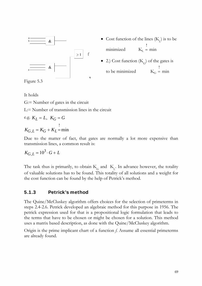
69
Figure 5.3
• Cost function of the lines (KL) is to be
minimized KL != min
• 2.) Cost function (K
G) of the gates is
to be minimized KG != min
It holds G:= Number of gates in the circuit L:= Number of transmission lines in the circuit e.g. K L K GL G= =,
K K KG L G L,!
min= + =
Due to the matter of fact, that gates are normally a lot more expensive than transmission lines, a common result is:
K G LG L, = ⋅ +103 The task thus is primarily, to obtain K
G and KL. In advance however, the totality
of valuable solutions has to be found. This totality of all solutions and a weight for the cost function can be found by the help of Petrick’s method.
5.1.3 Petrick’s method
The Quine/McCluskey algorithm offers choices for the selection of primeterms in steps 2.4-2.6. Petrick developed an algebraic method for this purpose in 1956. The petrick expression used for that is a propositional logic formulation that leads to the terms that have to be chosen or might be chosen for a solution. This method uses a matrix based description, as done with the Quine/McCluskey algorithm. Origin is the prime implicant chart of a function f. Assume all essential primeterms are already found.

70
f m1 m2 m3 p1 X X p2 X X p3 X X
Table 5.13 For every primeterm pi Petrick defines a Boolean variable ei, for which holds: ei :=
I if pi covers a minterm mj 0 if pi doesn’t cover a minterm mj
Petrick’s method now indicates the alternative choices of covering primeterms pi for every minterm mj. For the example it thus holds PAm1 = e1 + e2 PAm2 = e2 + e3 PAm3 = e1 + e3 As every minterm has to be covered in the petrick expression, a conjunction of the petrick expressions of the minterms has to follow. For the example it holds PA = (e1 + e2 ) • (e2 + e3) • (e1 + e3) = (e1 e2+ e1e3 + e2 e2 + e2 e3) • (e1 + e3) = e1 e2 e1+ e1e3 e1 + e2 e2 e1 + e2 e3 e1+ e1 e2 e3+ e1e3 e3 + e2 e2 e3 + e2 e3 e3
= e1e2e1+ e1e3e1 + e2e2e1 + e2e3e1+ e1e2e3+ e1e3e3 + e2e2e3 + e2e3e3
= e1e2+ e1e3 + e2e1 + e2e3e1+ e1e2e3+ e1e3 + e2 e3 + e2e3 (1) (2) (1) (3) (3) (2) (4) (4) = e1e2+ e1e3 + + e2e3e1+ + + e2 e3 With it, there exist 4 solutions in total. (This number was unknown, jet): PA = p1p2 + p1p3 + p2p3 + p1p2p3 These solutions have to be weighted now for the cost function. Therefore the following example has to be considered: Example: Given the function f with 4 variables and the following prime implicant chart
Objective of minimization: Minimum length: ∑ +=i
1i ip LiteraleL(f)
Whereas i is considered the outputs of pi (Only one output is considered here)

71
Reference number of mi equals its binary value: 0= 0000; 2 = 00I0 etc mi Cost function pk 0 2 4 11 12 14 16 ck p1 24xx x x 2 p2 23xx x x 2 p3 134 xxx x x 3 p4 134 xxx x 3 p5 124 xxx x x 3 p6 134 xxx x x 3 p7 123 xxx x x 3 ck : Number of (input)variables in pi
Table 5.14
The petrick expression can be computed to (practice at home)
IpppppppppppppppppppppppPA
I)p(p)p(p)p(pp)p(p)p(p)p(pPA!
75421754326543154327641
!
3173214756265
=++++=
=+⋅+⋅+⋅⋅+⋅+⋅+=
⇒ There exist 5 solutions, namely Interpretation: Number of Primeterms
L1: 7641 pppp +++ KL1=Σck=11 KG1=4 L2: 5432 pppp +++ KL2=11 KG2=4 L3: 65431 ppppp ++++ KL3=14 KG3=5 L4: 75432 ppppp ++++ KL4=14 KG4=5 L5: 75421 ppppp ++++ KL5=13 KG5=5
The solutions L1 and L2 are therefore the best to choose and they are equally well suitable.

72
5.1.4 Proceeding in combinational circuit synthesis
In circuit synthesis (combinatorial circuit) the following scheme can be used: 1. Evaluate the number of input- & output-variables from the specification of
the problem. 2. Describe the relations between the inputs & outputs of the circuitry.
=> Set up the truth table. 3. From the truth table, derive the CNF or DNF and simplify.
=> Set up a function, a KV map; Quine/McCluskey Algorithm => Evaluate the minimization result (Optimization), e.g. Cost function
4. If necessary transform the circuit to NAND/NAND and respectively NOR/NOR structure.
5. Draw the circuit.
5.2 State machine minimization
Most of the circuits, discussed up to now were combinatorial circuits. In these circuits, the outputs at a certain time (apart from propagation delay times) are only depending on the inputs at the same time. Sequential circuits’ outputs however are also depending on former inputs. In addition to combinational devices, sequential circuits also consist of memory elements like flip-flops. The stored information is characteristic for the state of the sequential circuit. A circuit with n binary storage elements can be in one of 2n possible states. Sequential circuits can be constructed synchronously or asynchronously. The state of synchronous sequential circuits only changes at well defined points in time, controlled by one clock-signal. Asynchronous sequential circuits don’t behave like that. There the function of the circuit depends on certain additional boundary-conditions which can vary by construction or operation. These circuits are a lot more complex and difficult to design therefore bigger sequential circuits are normally designed as synchronous circuits. In the following we will only deal with synchronous circuits. For the treatment of asynchronous ones, referred literature may be used.

73
5.2.1 Repetition: State Machines
State machine theory is suitable for the synthesis of synchronous circuits. The general state machine model will be determined by the following parameters: X: Input set/Vector Y: Output set/Vector Z: State set/Vector
or as an illustration of components :
figure 5.4: General State Machine Model The changes in states will be described by a transition function (e.g. g) . The output vector Y is derived from the output function (e.g. f). For clarification of the time sequences highly set indices will be used. With this follows, for the description of a state machine in vector form: Input vector: Xn State vector: Zn State transition function: g(Xn,Zn) Next state vector: Zn+1= g(Xn,Zn) Output function: f(Xn,Zn) Output vector: Yn= f(Xn,Zn) Mealy-State Machine
A Mealy-State Machine is defined through its’ Output function f: Yn = f(Xn,Zn) as well as State transition function g: Zn+1 = g(Xn,Zn)

74
figure 5.5: Mealy-State Machine Model Moore-State Machine
A Moore-State Machine is defined through its’ Output function h: Yn = h(Zn) State transition function g: Zn+1 = g(Xn,Zn)
figure 5.6: Moore-State Machine Model
another notation: Yn = f(Zn+1) results from replacing Zn+1 => Yn = f(g(Xn,Zn))
Comparison of the Mealy- and Moore-State Machines
1. In a stable state can appear in a Mealy-State Machine different output vectors in a Moore-State Machine only one output vector.
2. Mealy- and Moore-State Machines can be transformed into each other . 3. Yn = Zn: No output functions available => Medwedjew-State Machine
5.2.2 Forms of Describing State Machines
5.2.2.1 State machine tables
The state table (also State Machine Table) is a common form of illustrating state machines. It defines all details of the behavior of a state of a state machine. It

75
consists of three clumn areas. The first column contains a list of all possible states. The second column area contains a list of all possible input combinations in its first row. All other elements inside this matrix give the next states depending on the combination of actual states and possible inputs. Therefore it is a representation of the state transition function, see Table 5.15. The same table can be used to assign the output values to the next states resulting from the output function. The combination of both tables leads to the full state machine table as given in Table 5.17. (uncoded illustration): Transition Table
x1 x2 ..... xi ..... xk z1
zij=g(xi,zj)
z2 . . zj . . zl
Table 5.15 Transition table
Output table
x1 X2 ..... xi ..... xk z1
yij=f(xi,zj)
z2. . zj. . zl
Table 5.16: Output tableState table
x1 x2 ..... xi ..... xk z1
zij/yij
z2 . . zj . . zl
Table 5.17 state table The state table illustrated above is equivalent to a Mealy-State Machine. In the state table of a Moore-State Machine, only the next state will be entered in the Transition table. As the output function is only a function of the actual state and is independent of the input values xi, the output will be noted in a further column (the third column area):

76
State table of a Moore State Machine
x1 x2 ..... xi ..... xk z1
zij
y1 z2 y2 . . . . zj yu . . . . zl yv Table 5.18: State table of a Moore Machine If certain elements zij and/or yij, are missing one speaks of an incompletely determined state machine, otherwise the machine in completely determined. Application of the State Table for the a) Analysis of circuits b) Synthesis of circuits
Revision „Fundamentals of Computer Engineering 1“ 1. Definition of an In- and Output variable 2. Choice of type of state machine (Moore, Mealy,…) 3. State coding 4. Choice of type of flip flop and calculation of the flip-flops input functions 5. Design of the circuit for the state transition function 6. Design the circuit for the output function 7. Eventual transformation of the logical expressions into suitable structured
expressions 8. Application in the circuit diagram
5.2.2.2 State-Transition Diagram
A state transition diagram is used to for graphical representation of a state machine. A graph is composed of nodes and edges. The nodes are assigned the states of the state machine. This follows that a state machine is composed of A finite number of nodes (circle) The connecting lines between the nodes; the edges. Each edge is a transition
between two states. Arrows on the edges show the direction of the transistion (directed graph). A sequence (chain) of edges is called a path. In a connected graph, every node is reachable by every other node by at least one path.
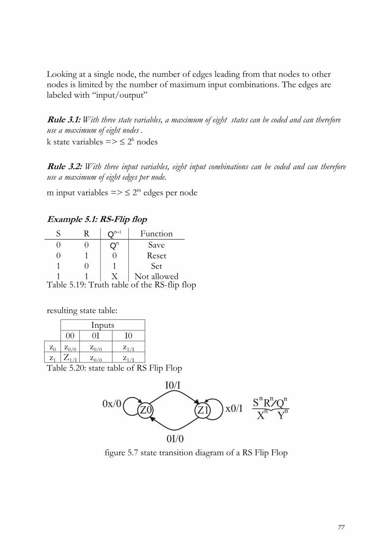
77
Looking at a single node, the number of edges leading from that nodes to other nodes is limited by the number of maximum input combinations. The edges are labeled with “input/output” Rule 3.1: With three state variables, a maximum of eight states can be coded and can therefore use a maximum of eight nodes . k state variables => ≤ 2k nodes Rule 3.2: With three input variables, eight input combinations can be coded and can therefore use a maximum of eight edges per node.
m input variables => ≤ 2m edges per node
Example 5.1: RS-Flip flop
S R 1+nQ Function 0 0 nQ Save 0 1 0 Reset 1 0 1 Set 1 1 X Not allowed
Table 5.19: Truth table of the RS-flip flop resulting state table:
Inputs 00 0I I0
z0 z0/0 z0/0 z1/I z1 Z1/I z0/0 z1/I
Table 5.20: state table of RS Flip Flop
figure 5.7 state transition diagram of a RS Flip Flop
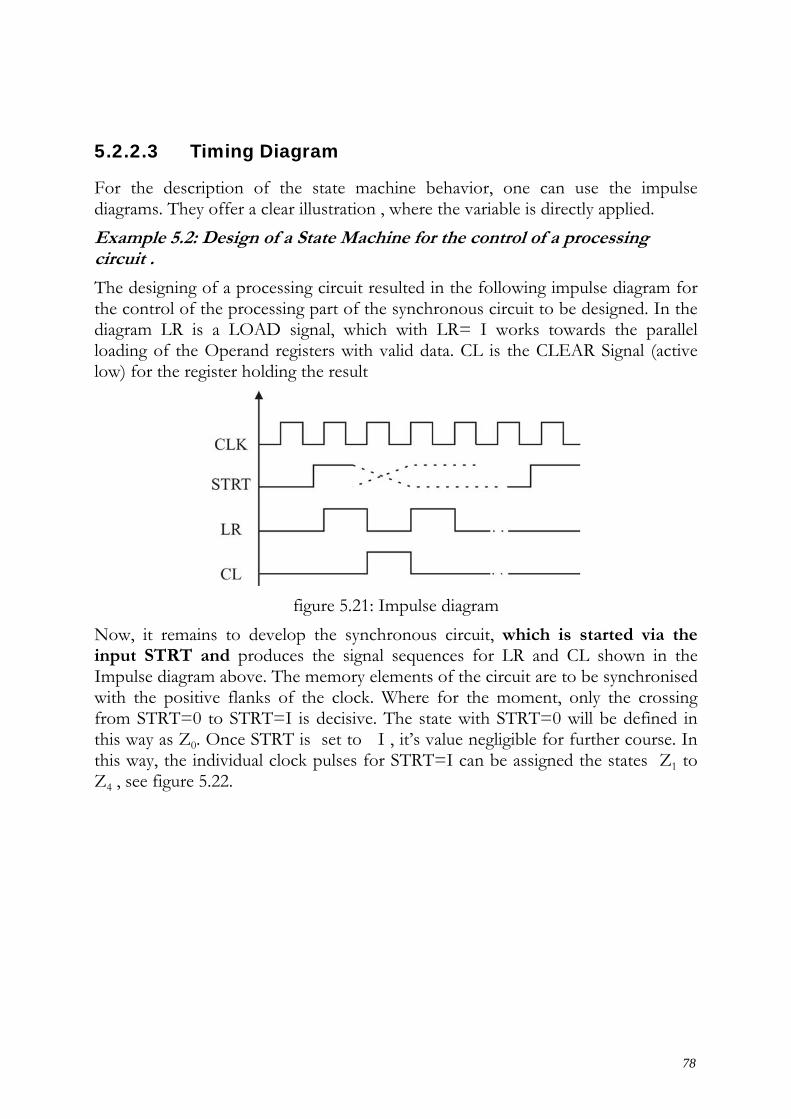
78
5.2.2.3 Timing Diagram
For the description of the state machine behavior, one can use the impulse diagrams. They offer a clear illustration , where the variable is directly applied. Example 5.2: Design of a State Machine for the control of a processing circuit .
The designing of a processing circuit resulted in the following impulse diagram for the control of the processing part of the synchronous circuit to be designed. In the diagram LR is a LOAD signal, which with LR= I works towards the parallel loading of the Operand registers with valid data. CL is the CLEAR Signal (active low) for the register holding the result
figure 5.21: Impulse diagram
Now, it remains to develop the synchronous circuit, which is started via the input STRT and produces the signal sequences for LR and CL shown in the Impulse diagram above. The memory elements of the circuit are to be synchronised with the positive flanks of the clock. Where for the moment, only the crossing from STRT=0 to STRT=I is decisive. The state with STRT=0 will be defined in this way as Z0. Once STRT is set to I , it’s value negligible for further course. In this way, the individual clock pulses for STRT=I can be assigned the states Z1 to Z4 , see figure 5.22.

79
figure 5.22: Impulse diagram and corresponding states
With Z4 the state machine reaches it’s final state and LR=CL=0. Before running a new sequence of states STRT must be set to = for at least one clock pulse, i.e. change the state machine once into the state Z0. The state Z0 will be described in the illustrated relation as „sharper“ state. The state Z4 leads the circuit into independency from STRT in the sharp state or remains in Z4. Due to this, the state table can now be positioned.
Z STRT=0 STRT=I LR CL Z0 Z0 Z1 0 0 Z1 Z2 Z2 I 0 Z2 Z3 Z3 0 I Z3 Z4 Z4 I 0 Z4 Z0 Z4 0 0 Table 5.23: state transition table for impulse diagram in figure 5.22
5.2.3 Trivial state machine minimization
The aims of state machine minimization will be discussed based on the Mealy State Machine example illustrated in figure 5.10 . In the example K1 and K2 show the combinatorial circuit parts of the state machine. The states are realized in Block Z.
figure 5.10: Mealy-State Machine
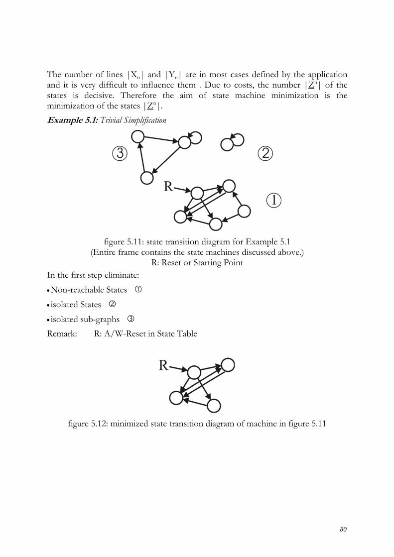
80
The number of lines |Xn| and |Yn| are in most cases defined by the application and it is very difficult to influence them . Due to costs, the number |Zn| of the states is decisive. Therefore the aim of state machine minimization is the minimization of the states |Zn|. Example 5.1: Trivial Simplification
figure 5.11: state transition diagram for Example 5.1
(Entire frame contains the state machines discussed above.) R: Reset or Starting Point
In the first step eliminate: • Non-reachable States • isolated States • isolated sub-graphs Remark: R: A/W-Reset in State Table
figure 5.12: minimized state transition diagram of machine in figure 5.11
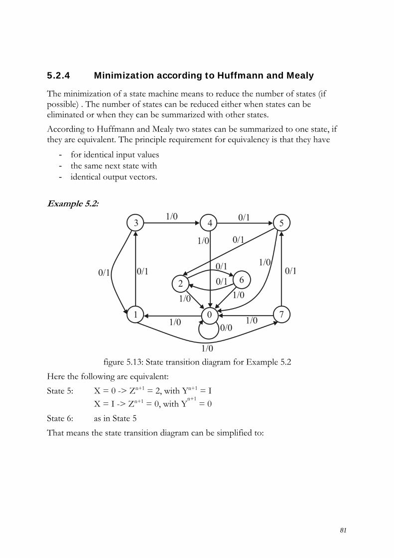
81
5.2.4 Minimization according to Huffmann and Mealy
The minimization of a state machine means to reduce the number of states (if possible) . The number of states can be reduced either when states can be eliminated or when they can be summarized with other states. According to Huffmann and Mealy two states can be summarized to one state, if they are equivalent. The principle requirement for equivalency is that they have
- for identical input values - the same next state with - identical output vectors.
Example 5.2:
figure 5.13: State transition diagram for Example 5.2
Here the following are equivalent: State 5: X = 0 -> Zn+1 = 2, with Yn+1 = I
X = I -> Zn+1 = 0, with Yn+1
= 0 State 6: as in State 5 That means the state transition diagram can be simplified to:

82
figure 5.14: simplified state diagram for machine in figure 5.13
Minimization is likewise (and more systematic in the process) possible in the state table.
Zn Zn+1 Yn Yn+1
X=0 X=I X=0 X=I0 0 1 0 0 0 1 3 7 V I 0 2 6 0 I I 0 3 1 4 I I 0 4 5 0 0 I 0 5 2 0 I I 0 6 2 0 I I 0 7 5 0 0 I 0
Table 5.24: state transition table for machine in figure 5.13 V: dependent on previous state From the table it follows immediately that: State 6 is identical to State 5 State 7 is identical to State 4 In this way the states 6 and 7 can be eliminated and the state table can be updated respectively:
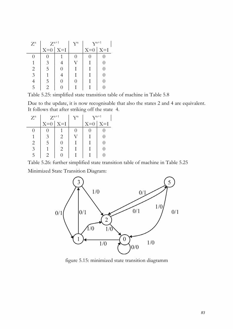
83
Zn Zn+1 Yn Yn+1 X=0 X=I X=0 X=I0 0 1 0 0 0 1 3 4 V I 0 2 5 0 I I 0 3 1 4 I I 0 4 5 0 0 I 0 5 2 0 I I 0
Table 5.25: simplified state transition table of machine in Table 5.8 Due to the update, it is now recognisable that also the states 2 and 4 are equivalent. It follows that after striking off the state 4.
Zn Zn+1 Yn Yn+1 X=0 X=I X=0 X=I0 0 1 0 0 0 1 3 2 V I 0 2 5 0 I I 0 3 1 2 I I 0 5 2 0 I I 0
Table 5.26: further simplified state transition table of machine in Table 5.25 Minimized State Transition Diagram:
figure 5.15: minimized state transition diagramm

84
5.2.5 The Moore Algorithm
In addition to the above mentioned equivalence, there exists a further form of equivalence. Assuming that, in the next state rows of two states there are states
lk ZZ , that can be summarised. Then, there could be, after summarising lk ZZ , once again row similarities. Example 5.3: The following state table is given.
0201401043124320324110410YcbaZ
Table 5.27: state transition table for Example 5.3 The principle requirement for each summary is as before, that the associated output of the states are equal. We will initially consider the states 0 and 2 for which this condition is fulfilled.
- Input b : equal next state : 4 - Inbut b : when 0, 2 can be summarised (hypothesis), the equal next
state (remains in it’s state) - Input a: only equal next state when, 1/3 can be summarised.
=> This is the case under the same conditions The equivalence identified in this way, will be described as „1“-equivalence and is eventually also be determined via the method of „closely(sharply) looking“ . It is however better to aim for a procedure, which possesses general validity. The MOORE-Algorithm exists hereby for searching for the k-equivalent states. This procedure works iteratively and finds the minimal partition (End class), where the blocks of this partition illustrate the minimum state set.
1. Step: Set 0-equivalence to 0-equivalent are in the example, all states with the same output.
{ }
äquivalent0 jeweils sind4 und 3 1, sowie2 und 0 ZuständeDieBB
BBP:hier
−==
=
)4,3,1()2,0(
,02
01
02
010
85
2.Step: Iteration - To find the k-equivalents: search blocks of the (k-1)-equivalents for next
states upon entering the same input.
- The block 1−kiB disintegrates into k
xB and kyB , when the next states of the
block 1−kiB fall into different blocks of (k-1)-equivalents; otherwise the states
are k-1-equivalent. - Aborting the iteration: when no more further fragmentation is possible .
Example 2.3 (Continuation)
Table 5.28: Investigating on “1“-equivalence Iteration: Investigating on „2“-equivalence
Table 5.29: “1”-equivalent state transition table States (0, 2) and (1,3) and (4) are “1” equivalent The minimized state machine consists of three states

86
Re-tranformation Rotation of the Moore-Table
Table: 5.30: resulting Moore-table Table 5.31: Resulting state transition table
Coding, and so on.
5.2.6 Algorithmic Formulation of the Minimization by Moore:
Definition: Two states Zm and Zn of a Moore State Machine are k-equivalent, when for every subsequence α of the possible sequences of inputs with α ≤ k vectors it is valid that:
g(Zm, α) = g(Zn, α) Considerable is a systematic comparison of all sub sequences with the variable k. However, a systematic search of the k-equivalence classes beginning with the 0-equivalence can be constructed.
− All states with identical exits illustrate 0-equivalence classes. − Should states be k-equivalent, this way they are also (k-1)-equivalent. For (Mk ⊆
Mk-1)- a (k-1)-equivalence is proven, in this way k-equivalent states illustrate exactly the subset of the (k-1)-equivalent states, which via an arbitrary input vector are once again passed into (k-1)-equivalence classes
− The search for highly valued k-equivalences must be continued, until it is proven that
− A state set is k-equivalent and (k+1)-equivalent (and therefore k+2, k+....);
− These states are equivalent w.r.t. arbitrary input sequence or/and − State sets now only contain a single element; − this state is therefore equivalent to no other.

87
figure 5.16: Moore-algorithm
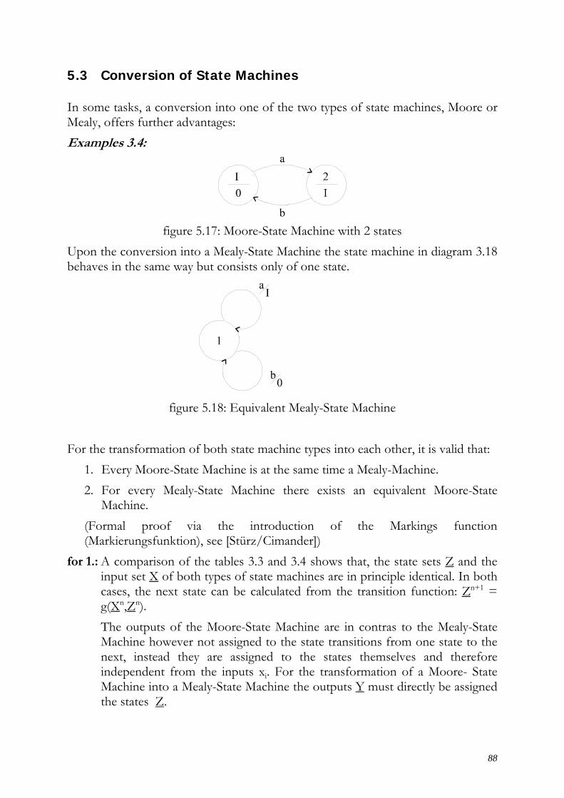
88
5.3 Conversion of State Machines
In some tasks, a conversion into one of the two types of state machines, Moore or Mealy, offers further advantages: Examples 3.4:
figure 5.17: Moore-State Machine with 2 states
Upon the conversion into a Mealy-State Machine the state machine in diagram 3.18 behaves in the same way but consists only of one state.
figure 5.18: Equivalent Mealy-State Machine
For the transformation of both state machine types into each other, it is valid that:
1. Every Moore-State Machine is at the same time a Mealy-Machine. 2. For every Mealy-State Machine there exists an equivalent Moore-State
Machine. (Formal proof via the introduction of the Markings function (Markierungsfunktion), see [Stürz/Cimander])
for 1.: A comparison of the tables 3.3 and 3.4 shows that, the state sets Z and the input set X of both types of state machines are in principle identical. In both cases, the next state can be calculated from the transition function: Zn+1 = g(Xn,Zn). The outputs of the Moore-State Machine are in contras to the Mealy-State Machine however not assigned to the state transitions from one state to the next, instead they are assigned to the states themselves and therefore independent from the inputs xi. For the transformation of a Moore- State Machine into a Mealy-State Machine the outputs Y must directly be assigned the states Z.

89
Example 5.5:
Given is the Moore State Machine according to Table 5.32.
22313
12132
33121
321
yzzzzyzzzzyzzzzYxxxZ
Output function: Yn = h(Zn) State Transition function: Zn+1 = g(Xn,Zn) Table 5.32: State transition table of a Moore Machine The individual next state elements of the equivalent Mealy-State Machine do now derive, when the output function of the Moore State Machine is considered in the state transition table. For the Moore State Machine according to Table 5.16 it is valid that Yn = h(Zn), i.e. in component notation y1 = h(z2), y2=h(z3), y3=h(z1). Herewith ,the equivalent Mealy-State Machine results according to Table 5.17.
1223313
1231232
2331121
321
yzyzyzYyzyzyzzyzyzyzz
xxxZ
Table 5.33: State transition of a Mealy Machine which is equivalent to Table 5.32
for 2.: Not every Mealy-State Machine is at the same time a Moore-State Machine: should for example in a state transition diagram of a mealy machine the outputs on the edges which end on the same nodes not match, then this state machine is not a Moore-State Machine (since the respective nodes must be assigned several outputs). In order to obtain an equivalent Moore-State Machine, as many new nodes as the number of different outputs on the edges of original nodes must be directed from the nodes of the Mealy-State Machine. In general, a Moore-State Machine equivalent to a Mealy-State Machine has therefore more states as the original Mealy-State Machine.

90
Example3.6:
The Mealy-State Machine according to Table 5.18 should be transformed into an equivalent Moore-State Machine.
42112
31221
21
yzyzzyzyzz
xx
Table 5.34: State transition table of a Mealy Machine The next states 1+n
kz of the Mealy-State Machine are included in the matrix elements [xi,zj] and can be calculated from the transfer function of the Mealy-State Machine:
1+nkz = g(xi,zj) ≡ [xi,zj]
Thereby in the Mealy-State Machine appear the following next states each with different outputs and therefore they have to be decomposed in new states z* with according outputs, in order to transform into a Moore-State Machine. For the assignment of the new states of the Moore-State Machine to the original states of the Mealy-State Machine the following correlation holds:
{ } [ ] [ ] [ ] [ ]{ }22122111*4
*3
*2
*1
* ,,,,,,,,,, ZXZXZXZXzzzzZ ==
Or by components: z1
* = [x1,z1] = z2/y2 with assigned output y2 z2
*= [x1,z2] = z1/y1 with assigned output y1 z3
*= [x2,z1] = z1/y3 with assigned output y3 z4
*= [x2,z2] = z2/y4 with assigned output y4
This results in the following first structure of an equivalent Moore-State Machine.
[ ][ ][ ][ ] 422
*4
312*3
121*2
211*1
21
,,,,
yzxzyzxzyzxzyzxz
xx
====
Table 5.35: First structure of a Moore Machines state transition table which is equivalent to Table 5.34

91
The next states of the Moore-State Machine can now be determined by the transfer function g*(xi,zj*) of the Moore-State Machine. Thereby it holds for the state-variables zj* the correlation indicated above to the original Mealy-State Machine. Therefore the next states of the Moore-State Machine are determined as:
1* +nkz = g*(xi,zj*) with zj* = [xi,zj] = g (xi,zj) ≡ zk
Determination of the next states Next state [x1,z1*]:
1* +nkz ≡ [x1,z1*] = g*(x1,z1*) with z1* ≡ [x1,z1] = g (x1,z1) = z2
1* +nkz ≡ [x1, z2] = with z2*
Next state [x1,z2*]:
1* +nkz ≡ [x1,z2*] = g*(x1,z2*) with z2* ≡ [x1,z2] = g (x1,z2) = z1
1* +nkz ≡ [x1, z1] = with z1*
Next state [x1,z3*]:
1* +nkz ≡ [x1,z3*] = g*(x1,z3*) with z3* ≡ [x2,z1] = g (x2,z1) = z1
1* +nkz ≡ [x1, z1] = with z1*
In adequate manner, the remaining states of the Moore-State Machine can be determined. It follows the equivalent Moore-State Machine depicted in Table 5.36.
4*4
*2
*4
3*3
*1
*3
1*3
*1
*2
2*4
*2
*1
21
yzzzyzzzyzzzyzzz
xx
Table 5.36: equivalent state transition table of a Moore Machine
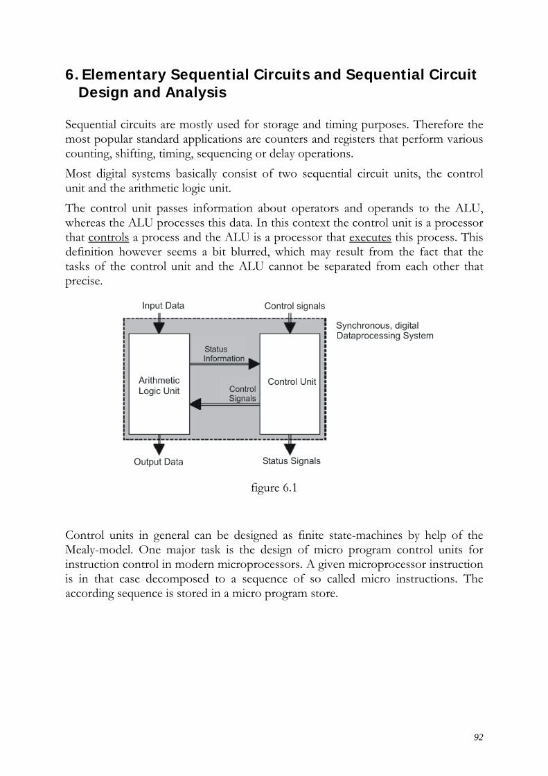
92
6. Elementary Sequential Circuits and Sequential Circuit Design and Analysis
Sequential circuits are mostly used for storage and timing purposes. Therefore the most popular standard applications are counters and registers that perform various counting, shifting, timing, sequencing or delay operations. Most digital systems basically consist of two sequential circuit units, the control unit and the arithmetic logic unit. The control unit passes information about operators and operands to the ALU, whereas the ALU processes this data. In this context the control unit is a processor that controls a process and the ALU is a processor that executes this process. This definition however seems a bit blurred, which may result from the fact that the tasks of the control unit and the ALU cannot be separated from each other that precise.
figure 6.1
Control units in general can be designed as finite state-machines by help of the Mealy-model. One major task is the design of micro program control units for instruction control in modern microprocessors. A given microprocessor instruction is in that case decomposed to a sequence of so called micro instructions. The according sequence is stored in a micro program store.
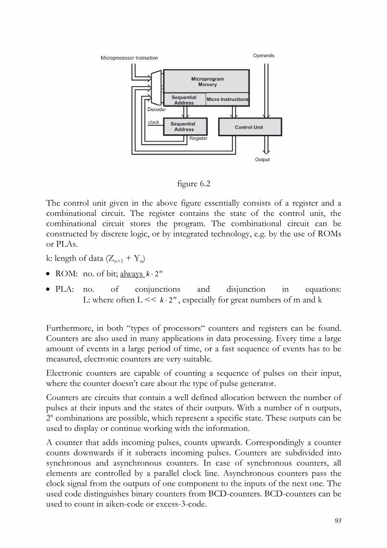
93
figure 6.2
The control unit given in the above figure essentially consists of a register and a combinational circuit. The register contains the state of the control unit, the combinational circuit stores the program. The combinational circuit can be constructed by discrete logic, or by integrated technology, e.g. by the use of ROMs or PLAs. k: length of data (Zn+1 + Yn)
• ROM: no. of bit; always mk 2⋅
• PLA: no. of conjunctions and disjunction in equations: L: where often L << mk 2⋅ , especially for great numbers of m and k
Furthermore, in both “types of processors“ counters and registers can be found. Counters are also used in many applications in data processing. Every time a large amount of events in a large period of time, or a fast sequence of events has to be measured, electronic counters are very suitable. Electronic counters are capable of counting a sequence of pulses on their input, where the counter doesn’t care about the type of pulse generator. Counters are circuits that contain a well defined allocation between the number of pulses at their inputs and the states of their outputs. With a number of n outputs, 2n combinations are possible, which represent a specific state. These outputs can be used to display or continue working with the information. A counter that adds incoming pulses, counts upwards. Correspondingly a counter counts downwards if it subtracts incoming pulses. Counters are subdivided into synchronous and asynchronous counters. In case of synchronous counters, all elements are controlled by a parallel clock line. Asynchronous counters pass the clock signal from the outputs of one component to the inputs of the next one. The used code distinguishes binary counters from BCD-counters. BCD-counters can be used to count in aiken-code or excess-3-code.
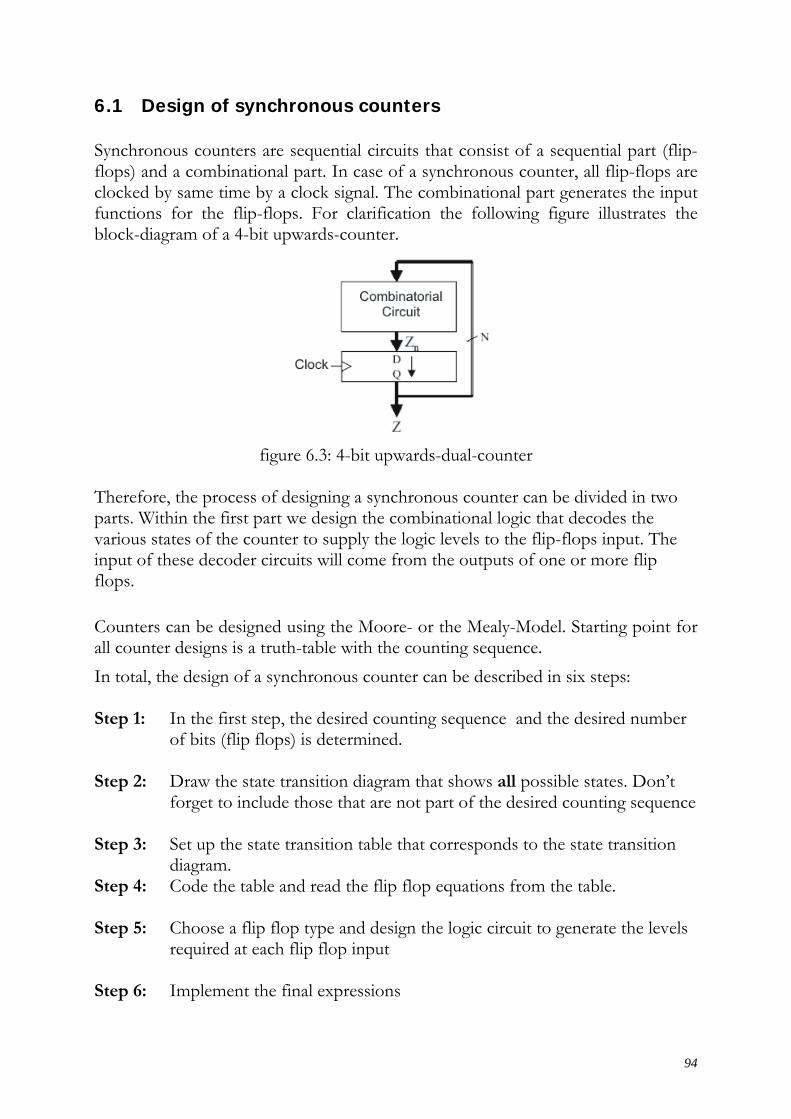
94
6.1 Design of synchronous counters
Synchronous counters are sequential circuits that consist of a sequential part (flip-flops) and a combinational part. In case of a synchronous counter, all flip-flops are clocked by same time by a clock signal. The combinational part generates the input functions for the flip-flops. For clarification the following figure illustrates the block-diagram of a 4-bit upwards-counter.
figure 6.3: 4-bit upwards-dual-counter
Therefore, the process of designing a synchronous counter can be divided in two parts. Within the first part we design the combinational logic that decodes the various states of the counter to supply the logic levels to the flip-flops input. The input of these decoder circuits will come from the outputs of one or more flip flops. Counters can be designed using the Moore- or the Mealy-Model. Starting point for all counter designs is a truth-table with the counting sequence. In total, the design of a synchronous counter can be described in six steps: Step 1: In the first step, the desired counting sequence and the desired number
of bits (flip flops) is determined. Step 2: Draw the state transition diagram that shows all possible states. Don’t
forget to include those that are not part of the desired counting sequence Step 3: Set up the state transition table that corresponds to the state transition
diagram. Step 4: Code the table and read the flip flop equations from the table. Step 5: Choose a flip flop type and design the logic circuit to generate the levels
required at each flip flop input Step 6: Implement the final expressions

95
Example 6.1: Design of a synchronous 4-bit upwards-counter. Step 1 The truth-table for the according count sequence is given in the following.
D C B A Z0 0 0 0 0 Z1 0 0 0 1 Z2 0 0 1 0 Z3 0 0 1 1 Z4 0 1 0 0 Z5 0 1 0 1 Z6 0 1 1 0 Z7 0 1 1 1 Z8 1 0 0 0 Z9 1 0 0 1 Z10 1 0 1 0 Z11 1 0 1 1 Z12 1 1 0 0 Z13 1 1 0 1 Z14 1 1 1 0 Z15 1 1 1 1
Table 6.1 There are 16 different outputs, where every output is assigned to a state. Therefore, the number of flip flops needed is calculated as ld(16)=4 => 4 flip flops are needed
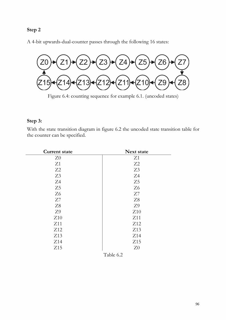
96
Step 2 A 4-bit upwards-dual-counter passes through the following 16 states:
Figure 6.4: counting sequence for example 6.1. (uncoded states)
Step 3:
With the state transition diagram in figure 6.2 the uncoded state transition table for the counter can be specified.
Current state Next state Z0 Z1 Z1 Z2 Z2 Z3 Z3 Z4 Z4 Z5 Z5 Z6 Z6 Z7 Z7 Z8 Z8 Z9 Z9 Z10 Z10 Z11 Z11 Z12 Z12 Z13 Z13 Z14 Z14 Z15 Z15 Z0
Table 6.2
97
Step 4:
Next a code needs to be chose, here the dual code Z0=0000; Z1= 0001, Z2= 0010…. and so on The coded state transition diagram is given in figure 6.5, the corresponding coded state transition table is shown in table 6.3
figure 6.5: counting sequence for example 6.1. (coded states)
Current state Next state
Q3 Q2 Q1 Q0 Q3+ Q2
+ Q1+ Q0
+ 0 0 0 0 0 0 0 1 0 0 0 1 0 0 1 0 0 0 1 0 0 0 1 1 0 0 1 1 0 1 0 0 0 1 0 0 0 1 0 1 0 1 0 1 0 1 1 0 0 1 1 0 0 1 1 1 0 1 1 1 1 0 0 0 1 0 0 0 1 0 0 1 1 0 0 1 1 0 1 0 1 0 1 0 1 0 1 1 1 0 1 1 1 1 0 0 1 1 0 0 1 1 0 1 1 1 0 1 1 1 1 0 1 1 1 0 1 1 1 1 1 1 1 1 0 0 0 0
Table 6.3: coded state transition table for example 6.1 From the coded state transition table the equations for the next state can be read and copied to a KV-Map, like shown in figure 6.6.

98
Q0+
Q2 Q3 I 0 0 I
I 0 0 I Q1 I 0 0 I I 0 0 I
Q0 Figure 6.6: KV-Map for Q0
+ From the KV-map it can be read
00 QQ =+
Step 5
For the realization by means of JK flip-flops the coefficients of the function have to be compared with the characteristic equation of the flip-flop.
QkQJQ +=+
From this it follows that:
J0=1 and 01 =k and respectively 00 1 Jk ==
Accordingly for the remaining next states it holds: Q1
+
Q2
Q3 0 I I 0 I 0 0 I Q1
I 0 0 I 0 0 0 0
Q0 Figure 6.7: KV-Map for Q1
+
10101 QQQQQ +=+
Anew coefficient comparison gives:
J1=Q0 and 01 QK = and respectively K1 = Q0= J1
Q2+
Q2
99
Q3 I I 0 0 I 0 I 0 Q1
I 0 I 0 I I 0 0
Q0 Figure 6.8: KV-Map for Q2
+
201210
01212022
)( QQQQQQ
QQQQQQQQ
++=
++=+
Comparison of coefficients:
102
012
QQK
QQJ
+=
=
DeMorgan:
2
01
10
102
JQQQQ
QQK
===
+=
Q3+
Q2 Q3 I I I I
I 0 I I Q1 0 I 0 0 0 0 0 0
Q0 Figure 6.9: KV-Map for Q3
+
01230213
01230323133
)( QQQQQQQQ
QQQQQQQQQQQ
+++=
+++=+
Comparison of coefficients:
0213
0123
QQQK
QQQJ
++=
=
DeMorgan
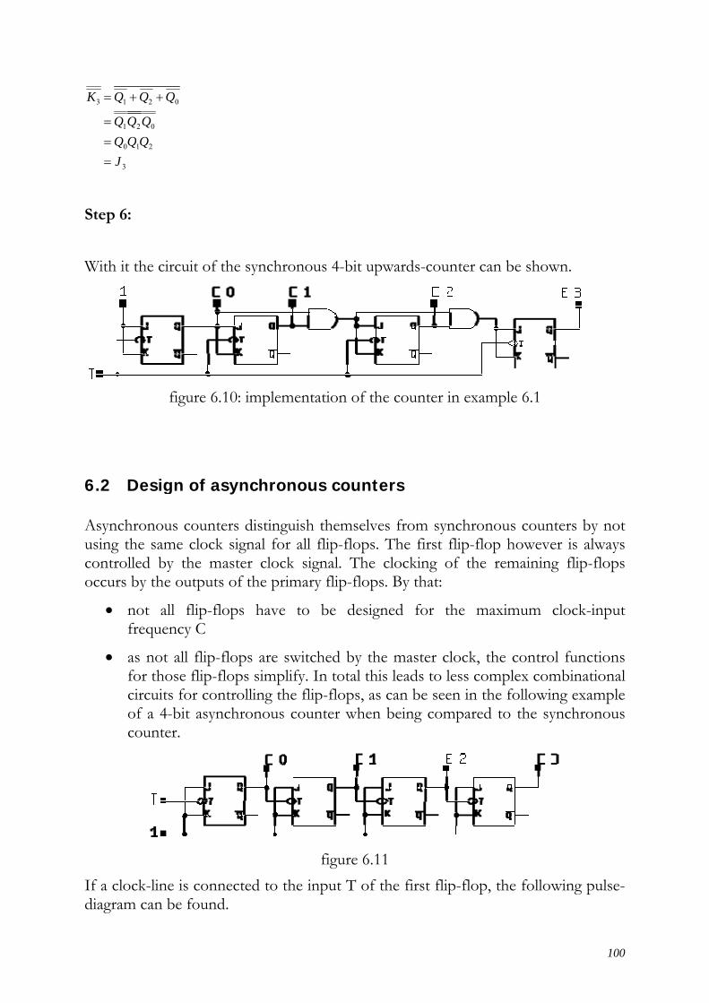
3
0
1
13
JQQQQ
QK
===
=
Step 6
With it
6.2 D
Asynchusing tcontroloccurs
• n
• a
coc
If a clodiagram
21
02
02
QQQQ
QQ ++
:
t the circui
figu
Design o
hronous cothe same clled by thby the out
not all flfrequency
as not all for those fcircuits forof a 4-bit counter.
ock-line is m can be f
it of the sy
ure 6.10: im
of async
ounters diclock signahe master tputs of th
lip-flops hC
flip-flops flip-flops sr controlliasynchron
connectedfound.
ynchronou
mplementa
chronous
istinguish tal for all fclock sign
he primary
have to
are switchsimplify. Inng the flipnous coun
d to the inp
us 4-bit upw
ation of the
s counte
themselveflip-flops. nal. The c
y flip-flops
be design
hed by then total this
p-flops, as nter when
figure 6.11put T of th
wards-cou
e counter i
ers
s from synThe first clocking o. By that:
ned for t
e master cs leads to lcan be seebeing com
1 he first flip
unter can b
in example
nchronousflip-flop hof the rem
the maxim
clock, the cless complen in the fompared to
p-flop, the
be shown.
e 6.1
s countershowever ismaining fli
mum cloc
control fulex combinfollowing e
the synch
e following
100
by not s always ip-flops
ck-input
unctions national example hronous
g pulse-

101
figure 6.12
This function can also be exhibited in a truth-table. If a value is assigned to every output (e.g. E0=1, E1=2, E2=4, E3=8), the dual-code is found and it can be proven that the counter runs through all numbers from 0000|2 to 1111|2 .
102
clock E3 E2 E1 E0 number 0 0 0 0 0 0 1 0 0 0 1 1 2 0 0 1 0 2 3 0 0 1 1 3 4 0 1 0 0 4 5 0 1 0 1 5 6 0 1 1 0 6 7 0 1 1 1 7 8 1 0 0 0 8 9 1 0 0 1 9 10 1 0 1 0 10 11 1 0 1 1 11 12 1 1 0 0 12 13 1 1 0 1 13 14 1 1 1 0 14 15 1 1 1 1 15 16 0 0 0 0 0 17 0 0 0 1 1
Table 6.4
6.3 Shift registers
In digital data-processing it is often reasonable to shift a piece of information stepwise, e.g. inside a memory chain. Such a memory chain is called shift register. Data are shifted by clock pulses about one or multiple positions, but only one position at one pulse. Shift registers are needed e.g. for basic arithmetic operations like multiplication and division. Both can be realized by an addition or respectively subtraction and a shift operation. Even only a shift operation represents a mathematical operation. If position-values are assigned to the outputs of a shift register then a shift of a dual number to the right corresponds to a division by 2 and respectively a shift to the left corresponds to multiplication with 2. From a circuit-based view the shift register as well as the counter consists of a pure sequential part and a pure combinational part. The data in the register are shifted by the clock pulses from one memory-cell to the next. Mostly a conversion of the data format is possible, such that serial inputs/outputs can be converted into parallel inputs/outputs.
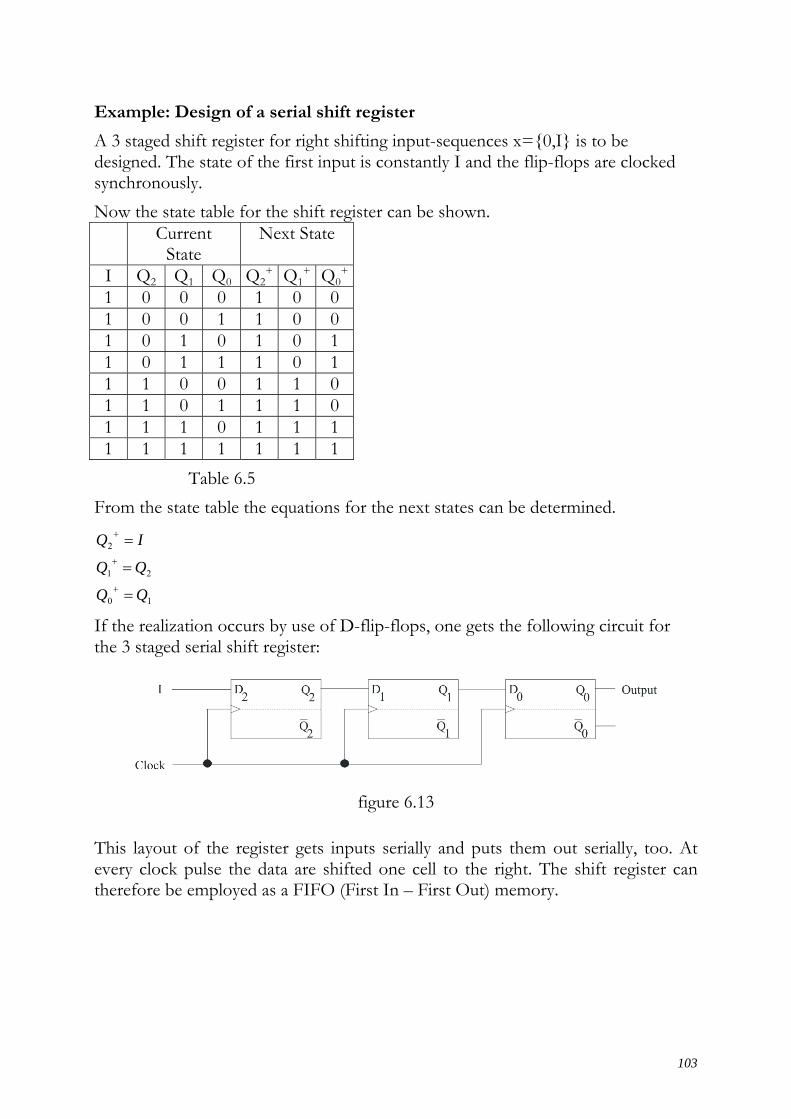
103
Example: Design of a serial shift register
A 3 staged shift register for right shifting input-sequences x={0,I} is to be designed. The state of the first input is constantly I and the flip-flops are clocked synchronously. Now the state table for the shift register can be shown.
Current State
Next State
I Q2 Q1 Q0 Q2+ Q1
+ Q0+
1 0 0 0 1 0 0 1 0 0 1 1 0 0 1 0 1 0 1 0 1 1 0 1 1 1 0 1 1 1 0 0 1 1 0 1 1 0 1 1 1 0 1 1 1 0 1 1 1 1 1 1 1 1 1 1
Table 6.5 From the state table the equations for the next states can be determined.
10
21
2
IQ
=
=
=
+
+
+
If the realization occurs by use of D-flip-flops, one gets the following circuit for the 3 staged serial shift register:
figure 6.13 This layout of the register gets inputs serially and puts them out serially, too. At every clock pulse the data are shifted one cell to the right. The shift register can therefore be employed as a FIFO (First In – First Out) memory.

Examp
Compa
10
21
2 1
QJ
QJJ
=
=
=
Circul
If the oflop insignal tend. Su
Series/
Other Those furtherinformIn the in serieshiftingPISO (
ple: Reali
arison of c
0
1
2
K
KK
=
ar shift re
output of n a shift rethat travelsuch a regis
/Parallel-
special tyare neede
r in parallemation in se
shift registes. Loading is done (Parallel In
ization wi
coefficients
1
2
0
Q
Q
=
=
=
egisters
the last flegister, thiss through ter can be
-Converte
ypes of shed when iel. Its coueries that oter conside
ng and savvia the cl
n - Serial O
ith JK-flip
s (Equatio
lip-flop is s is called this registeused as a
ers
hift registerinformatio
unterpart ioriginally wered now iving of thelock input
Out).
p-flops
ons have to
being cona circular
er comes bring count
figure 6.14
rs are theon arrives is the parawas put in it is possibe register it TS. This
o be expan
nnected tor shift regiback to theter.
4
e so calledin series,
allel/seriesparallel.
ble to inpuis done vishift regis
nded by (Q
o the inputister (ger.: e origin wh
d series/pa, but has s-converte
ut data in pia the inpuster is oft
xx QQ + ) ) g
t of the firRingschie
hen passed
arallel-conto be pro
er, which o
parallel andut TP whilen referre
104
gives:
rst flip-eber). A d to the
nverters. ocessed outputs
d shift it le serial
ed to as

The cothem pTP for
The ac
ounterpart parallel. Thparallel loa
cording sy
to the PIShis is also ading of th
ymbol for
SO is a shreferred to
he register
the describ
figure 6.15hift registero as SIPOis not req
figure 6.16bed shift r
figure 6.17
5 r that inpu
O (Serial Inquired here
6 registers lo
7
uts data sern - Parallele any more
oks as foll
rially and ol Out). The.
lows:
105
outputs he input

106
7. Testing digital circuits
7.1 Introduction
A requirement for the usage of computers for the testing of digital circuits is an appropriate model of the circuit under test. For that purpose one needs a circuit model and a definition of the fault-model that accounts for the appropriate technological fault mechanisms. Typically simulation tools contain a set of basic elements, the so called “primitives“ from which every system can be build up and which also give reference for the chosen fault model. The usage of models to describe the circuit that is to be tested and its faults brings simplifications on the one hand, but blurred test declarations on the other hand. The desired maximized simplification of the model with a maximum number of details at the same time permanently lead to new abstractions of the model, caused by the evolution of circuit technologies. In figure 7.1 some important steps of this evolution are shown. The level of abstraction of the models in figure 7.1 rises starting from the structural models (technology, transistor, gate). Real faults occur only on the technology-layer and are just indicated on higher layers. The significance of these fault-models thus always has to be evaluated in combination with the used circuit-model. In the following overview the most important properties of the circuit-models from figure 7.1 are summarized.
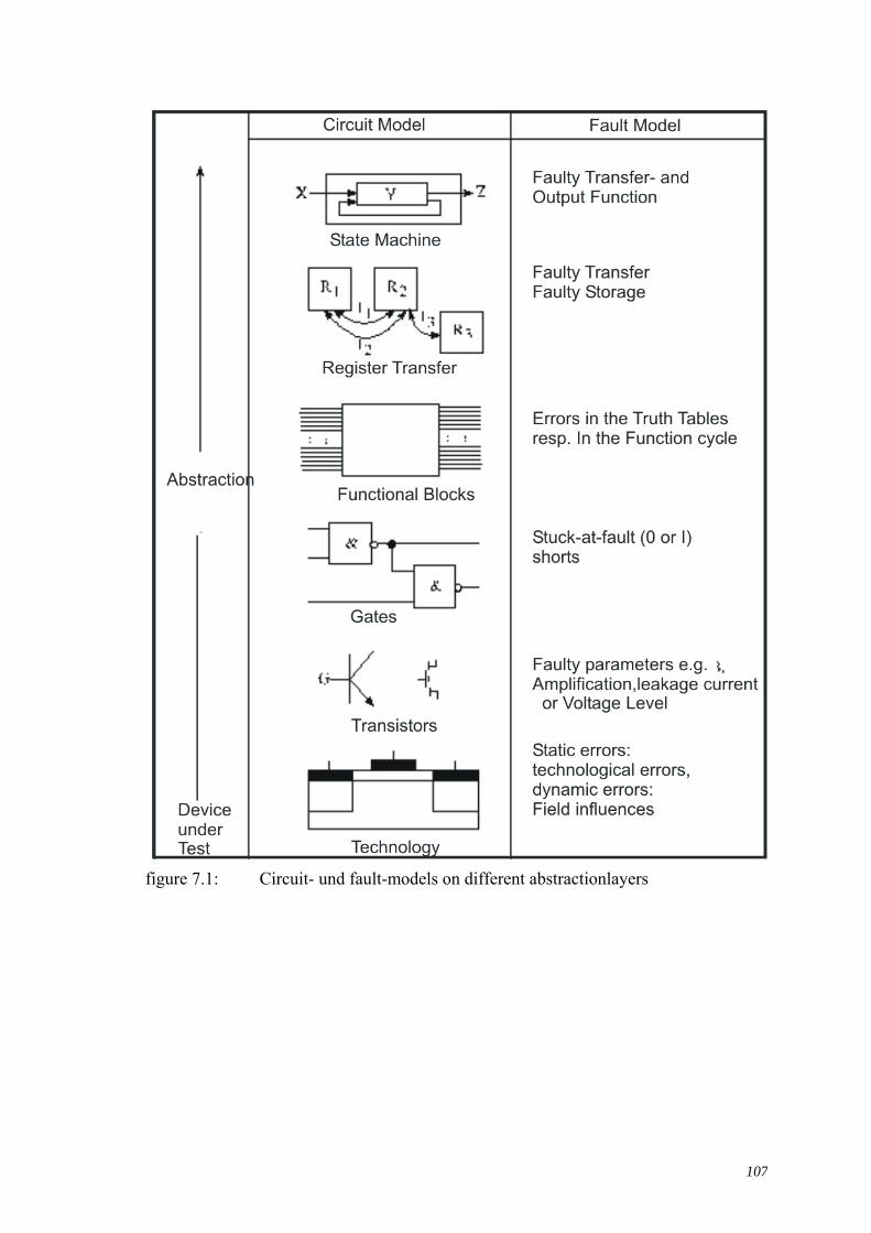
107
figure 7.1: Circuit- und fault-models on different abstractionlayers
108
Technology-Layer
Here the base is the illustration of a circuitry as a network of equivalent circuits of the single electronic devices, where their physical properties can be controlled by parameters. For these devices, different voltages & currents can be calculated, but there exist economical limits which are given by the immense effort for extremely exact simulations (the limit for the number of single electronic devices inside a circuit lies at about 100). Tests related to the semiconductor-structure are much device-specific or respectively manufacturer-specific, that they don’t lead to a general model and that they can only be performed by the manufacturers themselves. The gained conclusions relate to the behavior on the physical / technnological layer and are inapplicable for development and analysis of test-patterns for ordinary PCBs. Transistor-Layer On this layer the user executes his parametric test. Thereby compliance with treshold values such as voltage levels or leakage currents for input- and output transistors is checked, which is given in the corresponding data-sheets. Modeling a complex integrated circuit on the transistor-layer normally fails because of the immense effort and missing documentation. Gate-Layer This is the lowest layer for logical design of digital systems and with it the best suitable layer to conduct tests on the logical behavior of a circuit. The gate-representation is based on the behavior of logic circuits realized in bipolar technology and permits it to exhibit logical and physical behavior (combining input variables, timing, etc.). The used unidirectional signal-flow also complies with real behavior of bipolar technology. For MOS circuits a pure gate representation is not always possible. However when considering the special properties of MOS transistors, it is possible to combine them to equivalent gate-models which are called „complex logic gates“, which then can be expressed easily via gate logic. These gates normally don’t have a direct relation to the transmission lines and combinations inside the MOS circuit, but they only serve as a description for this unit. Furthermore it is possible to design circuits in mixed representation by gate- and switch-models to represent reality at best.

109
Functional-Layer
By reason of economic advantages of a functional description, several methods to represent circuit-behaviour by a function have been developed: • Functional-blocks (e.g. Register, ALU, etc.) • Truth-tables (for combinatorial circuits) • Program-modules in a high level language, which describe the behaviour of the
blocks • Graphical illustration (e.g. Petri-nets) • And more methods as well as mixtures of these These possibilities are taken if the appropriate functions • are not available as structured models • exactly that part of the circuit shall not be considered in detail, but its existence
still is important for the operation of other elements or even the whole circuit. Register-Transfer-layer In the register-transfer layer the DUT is reduced to an appropriate set of registers and operators. The function of the device is to store data and to modify data while transferring. Automata-Layer This most abstract model allows multiple, simple representations of the DUT. Its’ function is described by the transfer- and output-function of the state machine, where those terms still give a lot of leeway for modeling and have to be concretized for every individual case. For practical purposes it results: • One always has to check if a given fault-model fits to the present circuit, or • Creation of an adequate fault-model • Details for a test (E.g. “detects 90% of…“) always have to be mentioned for a
circuit- and fault-model, together.
In the following we will only consider the gate-layer and the stuck at fault model.
7.2 Principles of testing
Faults may occur in various development steps, e.g.: Design faults like:
- Implementation doesn’t fulfill with the specification
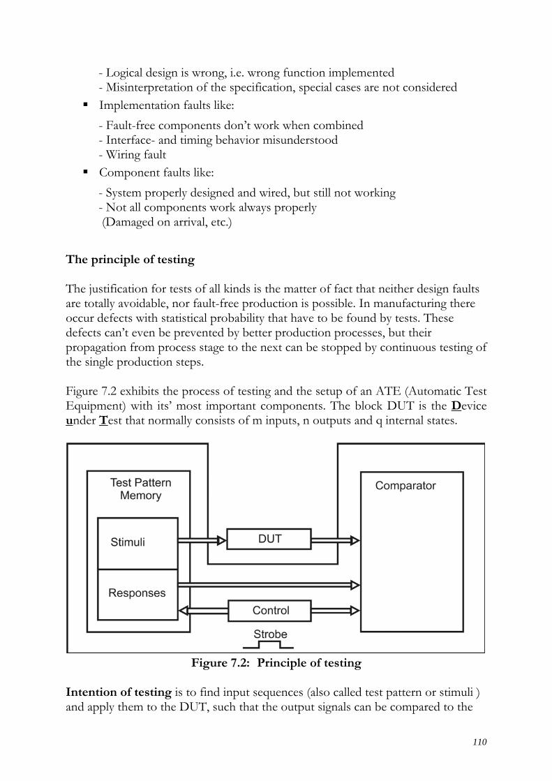
110
- Logical design is wrong, i.e. wrong function implemented - Misinterpretation of the specification, special cases are not considered
Implementation faults like: - Fault-free components don’t work when combined - Interface- and timing behavior misunderstood - Wiring fault
Component faults like: - System properly designed and wired, but still not working - Not all components work always properly (Damaged on arrival, etc.)
The principle of testing The justification for tests of all kinds is the matter of fact that neither design faults are totally avoidable, nor fault-free production is possible. In manufacturing there occur defects with statistical probability that have to be found by tests. These defects can’t even be prevented by better production processes, but their propagation from process stage to the next can be stopped by continuous testing of the single production steps. Figure 7.2 exhibits the process of testing and the setup of an ATE (Automatic Test Equipment) with its’ most important components. The block DUT is the Device under Test that normally consists of m inputs, n outputs and q internal states.
Figure 7.2: Principle of testing
Intention of testing is to find input sequences (also called test pattern or stimuli ) and apply them to the DUT, such that the output signals can be compared to the

111
expected outputs in the case of a fault free DUT. The stimuli are saved in the testpattern memory together with the correct outputs (responses) of the fault free circuit. Then the stimuli are forwarded to the DUT while the output of the DUT are forwarded to the comparator. The comparator then compares the present outputs with the expected (stored) outputs (responses) and creates a go/no-go decision. The control unit contains the test program that among others generates the addresses under which the stimuli and the responses are stored in the testpattern memory. Even though this process runs automatically it shouldn’t be forgotten that both the test pattern and the test program have to be delivered by the test engineer. In the following the class of DUTs is being restricted to digital circuits which then behave in a combinational or sequential way. In case of a combinational circuit for a complete test one would need up to 2m stimuli. In case of a sequential circuit even 2m q+ stimuli would be needed. example: Memory requirements a)Assumption: combinational circuit with m = 24 inputs s(timuli) = r(esponses) = 224 = 16M Words = 48 Mbyte (with 1 Word = 24 bit = 3 Byte) (All stimuli are independent from each other as it is a combinational circuit.) The required memory size arises to s + r = 96 Mbyte b) Assumption: sequential circuit here e.g. a microprocessor with m = 24 and q =100 That leads to s = r = 2124 Words ~ 3*1037 Byte
These patterns have to be created as a sequence as the DUT has to be considered a sequential circuit; with it a test program for time-accurate running of the test sequence is needed.
Time considerations Control in the ATE with 100 MHz => 10ns/Stimulus and with it the duration for the sequential circuit: 1037*10-8 sec ~ 1029 sec => 3,1721 years =1,16*1024 days (example: 2000 years = 7,3*105 days) => A test by applying all possible patterns is normally not possible
112
Consequences • Determination of
minimum sets of test patterns
⇒ Testpattern generation
• Evaluation of given test
patterns ⇒ Fault simulation: a fault-simulator is a tool
that cares for the weighing of the stimuli and calculates the fault coverage of a set of given test pattern.)
• Reducing the problems in
the DUT (Decrease the values of m and q)
⇒ Easy testable design (The evaluation of a circuit can be made via testability analysis)
The consequences given above also give the historical development due to the increasing complexity of DUTs. Nowadays the trend goes more and more to a combination of the available methods. An additional problem is the matter of fact that normally the ATE is at least one generation older than the DUT.
7.3 Overview on test mechanisms
Fully automated test generation
Starts from the circuit diagram and is possible in general. From an economical point of view it is justifiable only for relatively small circuits. One uses:
• Boolean difference • D-Algorithm • And respectively enhancements of the D-Algorithm
Heuristic test-pattern-generation
Test patterns are obtained by the experience and intuition of the test engineer. This method is used for complex circuits that cannot be tested by algorithmic means, or respectively if the exact circuit-structure is unknown.

113
Test-friendly design
All details about the circuit are known, actually the design can also be changed. Testability can be simplified very much by DFT (Design For Testability) or BI(S)T (Built-In-(Self-)Test). Testability analysis
Both of the newer methods, partitioning test-pattern-generation and inclusion of test-aids are naturally heuristic, i.e. their result is strongly depending on the users’ intuition. Caused by that, testability-analysis has been developed as another criterion for the decision of the test-engineer.
7.3.1 Important CAD-tools for test generation
Logic simulations are mainly used in the design phase, to verify that the circuit design behaves according to the original specifications. Within the scope of test generation logic simulations are used to determine the behavior of a fault-free circuit while certain stimuli are attached to the inputs. These patterns are used later on to compare to the real output of the circuit. Fault simulations are used to determine how many of all assumed faults are detectable by a set of given test pattern and therefore they deliver the fault coverage for this set of given test pattern. Normally the stuck-at fault-model is chosen. There, one considers that all production faults manifest in a jamming of the transmission lines at the logic values 0 or I. To limit computing-time it is assumed, that only one fault occurs at a given time. Automated test-pattern generation:
While logic- and fault-simulation only have to deliver signals from input to output, popular methods for test-pattern generation have to compute two phases:
Fault-signal propagation to the outputs of the circuit, and Backwards-simulation from the point of failure to the inputs to “inject” the
appropriate fault. Thereby normally a number of conflicts occur, i.e. single paths turn out to be not applicable and have to be replaced by others.

114
7.3.2 Application of test-tools in integrated systems
From the causes mentioned above, one can imagine that the effort in using these tools varies very strong. While in logic simulations there is a linear relationship n (n: number of gates) between computation-time and the size of the circuit, this relation rises to n2 in fault simulation and to n3 in automated test-pattern generation. The effort for testability-analysis of a circuit rises approximately linearly with the size of the circuit. Opposite to that apparently optimal behavior lies the fact that the testability-analysis provides only an approximation of the complexity and based on that fact adds to the mentioned tools, but cannot replace them. Facing the complexity of modern circuits, a combination of the classic tools has turned out to be the most effective solution (see figure 7.3).
a.) b.)
a) Iterative procedure assisted by a Test Pattern Generator and a Fault Simulator
b) Possible application of testability analysis ba) for redesign bb) for controlling the ATPG-Algorithm bc) as a substitute for fault Simulation figure. 7.3 application of test-tools in integrated systems
Due to the above mentioned guideline values for the effort for every tool, it is obvious that the process in 7.3 a) requires a huge amount of computation capacity. The process 7.3 b) shows the different possibilities for the use of testability-analysis. The three possibilities for testability-analysis can be employed in a lot of different ways in reality, where bc) has the least importance. The relevance of the other ways lies in the fact that the automated test-pattern generation either works with problem-sets that are a lot smaller (alternative ba) ), or by knowing the

115
complexity can be controlled very efficiently (alternative bb) ). Proceeding by means of figure 7.3 therefore can be done with less effort on computation-time and additionally this goes into the direction of the ideal process-model. Following the conceptional steps for building up a process-model mentioned here, single tasks have to be solved for the implementation. One aspect is the integration of design and tests regarding the test-equipment where especially the limited possibilities of test-machines compared to the high demands of the developers have to be considered. Furthermore, a consistent database has to be created, as both data-storage and data-transfer play an important role in a closed process model.
7.4 Faults and fault-models
Testing means to differentiate between faulty circuits and fault-free circuits. Recognition of faults in a production-line requires continuous observation of each step in the production process. Faults in the circuits can thereby occur in various phases of product design: Sources for faults:
• in raw material (crystal-faults) • in design
- logic faults (these are not covered in this section) • in production
- Non-uniform doping - Non-uniform etching - Masking faults - Bonding fault
• after production - Electrical overload / surge (while operating) - thermal overload - static discharge (prior to CMOS-circuits)
• Atommigration • in operation
- environmental factors - corrosion - micro-cracks - electromigration (material transportation)
The systematic acquisition of those and other effects occurs in fault-models.

116
figure 7.4: fault-classification: [MUT 75] A modification of the behavior of a circuit caused by a physical defect is called fault:
• logic faults: A logic fault manifests by the logic behavior of a circuit.
• parametric faults: Parametric faults change the operating parameters of a circuit, like speed, power-consumption or temperature behavior, etc.
• delay faults: Delay faults are malfunctions of the circuit, regarding the transition-time. They can be caused by parameter changes.
• intermittent faults: Faults, that occur only from time to time.
• permanent faults: Permanent faults are time-invariant. Logic faults are always permanent.
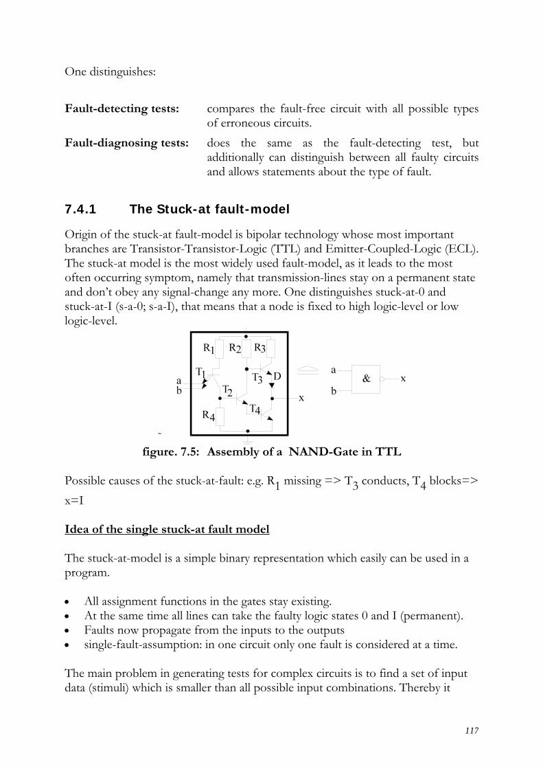
117
One distinguishes: Fault-detecting tests: compares the fault-free circuit with all possible types
of erroneous circuits. Fault-diagnosing tests: does the same as the fault-detecting test, but
additionally can distinguish between all faulty circuits and allows statements about the type of fault.
7.4.1 The Stuck-at fault-model
Origin of the stuck-at fault-model is bipolar technology whose most important branches are Transistor-Transistor-Logic (TTL) and Emitter-Coupled-Logic (ECL). The stuck-at model is the most widely used fault-model, as it leads to the most often occurring symptom, namely that transmission-lines stay on a permanent state and don’t obey any signal-change any more. One distinguishes stuck-at-0 and stuck-at-I (s-a-0; s-a-I), that means that a node is fixed to high logic-level or low logic-level.
figure. 7.5: Assembly of a NAND-Gate in TTL
Possible causes of the stuck-at-fault: e.g. R1 missing => T3 conducts, T4 blocks=> x=I Idea of the single stuck-at fault model The stuck-at-model is a simple binary representation which easily can be used in a program. • All assignment functions in the gates stay existing. • At the same time all lines can take the faulty logic states 0 and I (permanent). • Faults now propagate from the inputs to the outputs • single-fault-assumption: in one circuit only one fault is considered at a time. The main problem in generating tests for complex circuits is to find a set of input data (stimuli) which is smaller than all possible input combinations. Thereby it

118
generally holds that a fault is only detectable if the wrong behaviour that the fault causes is observable at the output. Example: Fault-matrix of an AND-Gate with three inputs
e1e2e3
a&
figure 7.6 In this circuit 8 single faults can occur: Fi, 1≤ i ≤ 8. These are characterized by the facts that one input remains at the logical state “0“ or at “1” or that the output stucks-at “0” or at “1”. For these faults the following fault-matrix can be constructed. The columns e1,…e4 contain the values for all possible input-pattern, the column a holds the responses to all input pattern in case of a fault free circuit. The columns F1..F8 contain the output values in case of an existing fault as indicated below the fault numbers Fi. Output at a specific fault e1 e2 e3 a F1
sa0/e1 F2
sa0/e2
F3 sa0/e3
F4 sa1/e1
F5 sa1/e2
F6 sa1/e3
F7 sa0/a
F8 sa1/a
0 0 0 0 0 0 0 0 0 0 0 0 1 1 0 0 1 0 0 0 0 0 0 0 0 1 2 0 1 0 0 0 0 0 0 0 0 0 1 3 0 1 1 0 0 0 0 1 0 0 0 1 4 1 0 0 0 0 0 0 0 0 0 0 1 5 1 0 1 0 0 0 0 0 1 0 0 1 6 1 1 0 0 0 0 0 0 0 6 0 1 7 1 1 1 1 0 0 0 1 1 1 0 1
Table 7.1 Some of the columns are identical, as the appropriate faults create the same erroneous behavior at the output. E.g. F1, F2, F3, F7. These faults indeed can be observed, but cannot be distinguished. Therefore it is sufficient to let only one of these remain in the matrix and delete the others.

119
With it one gets the following reduced matrix. Output at a specific fault e1 e2 e3 a F1
sa0/e1
F4 sa1/e1
F5 sa1/e2
F6 sa1/e3
F8 sa1/a
0 0 0 0 0 0 0 0 0 1 1 0 0 1 0 0 0 0 0 1 2 0 1 0 0 0 0 0 0 1 3 0 1 1 0 0 1 0 0 1 4 1 0 0 0 0 0 0 0 1 5 1 0 1 0 0 0 1 0 1 6 1 1 0 0 0 0 0 1 1 7 1 1 1 1 0 1 1 1 1
Table 7.2
In general: Multiple non-distinguishable faults can be combined to classes of equivalent faults, which then can be covered by one test. With it follows in general a reduction of the set of faults from 2m + 2 to m + 2 (with m = number of inputs). It is sufficient to find a test-pattern for one of each fault-class. Another question is if it is necessary to employ all input combinations for recognizing all possible faults. E.g.: Combination 1 (0,0,1): recognizes only fault 8 Combination 3 (0,1,1): recognizes F4 AND F8 Thus combination 3 additionally covers F4. Therefore all tests that only cover F8 can be deleted (F0, F1, F2, F4). By employing the combinations 3,5,6 & 7 all faults of the gate can be recognized. This number of test-patterns cannot be simplified any more. More definitions: Def. 1: In a combinational circuit that only contains (N)AND, (N)OR and
Inverters it is sufficient to test all stuck-at-faults at the primary inputs (PI) and fan-out nodes. The differentiability for diagnostic usage will be lost by that behavior however.

120
figure 7.7: Example circuit for Definition 1
7.5 Test generation
Objective of test generation (test-pattern computation) is to find test-patterns for the inputs of the circuit based on an exactly defined formulation, which allow to observe the circuits’ outputs and then distinguish between correct and erroneous output-data.
7.5.1 Boolean Difference
Originally this method was based on the circuit’s equation and is therefore independent from the implementation. In this case it delivers all tests for stuck-at faults at the primary inputs and outputs. In principle however it can be employed in dependence of the implementation, too by determining the functional equation of the circuit. Limits of that method are given by the size of the circuit. The method of the boolean difference is • independent of the implementation in principle - delivers the complete set of testpattern for all input variables, • can be employed independent of implementation - provides the set of testpattern with all possible paths - can also be used for internal nodes,

121
• is unhandy, as in the here treated form it works with formular manipulation (Alternative: Bochmann/Steinbach: Logic design with XBOOLE; this method is an example for computer based implementation for the solution of Boolean differences with the help of ternary vector-lists),
• in general too extensive, as all solutions have to be evaluated, but normally one test per fault is enough.
Derivation: Point of origin for these considerations is the expansion theorem: f (x ,x ,x ,..., x ) x f (x ,x ,..., x ,I, x ...x ) x f (x ,x ,..., x ,0,x ...x )1 2 3 n i 1 2 i 1 i 1 n i 1 2 i 1 i 1 n= ⋅ + ⋅− + − + The Boolean difference is the partial derivative of the function f with respect to the variable x, or when used with respect to all variables the total derivative. It is constructed by means of inserting first a I and then a 0 for the variable xi into the function f and then combining them with XOR. df (x)
dxf (x) f (x)
ix xi 1 i 0
= ⊕= =
df (x)dx
= f (x) f (x)
df (x)dx
= f (x ,x ,...., x ,I, x ...x ) f (x ,x ,...., x ,0,x ...x )
ix =1 x
i1 2 i-1 i +1 n 1 2 i-1 i +1 n
i i⊕
⊕
=0
The Boolean difference thus is always I if the functional characteristics of f related to xi=I and xi=0 are different. This exactly describes the fault-free case. By establishing the Boolean difference thus a path from the PI to the PO is enabled such that changes at the input can be observed at the output. That however means that all input combinations except xi are redundant. In total the following prepositions can be made:
dfdx
Ti
i
i 1
n
==∑ ===> non trivial solution : gives all possible test-patterns
dfdx
0i
= ===> f(x) ist independent from xi : the node xi is redundant
dfdx
Ii
= ===> f(x) only depends on xi : all variables except xi are
redundant
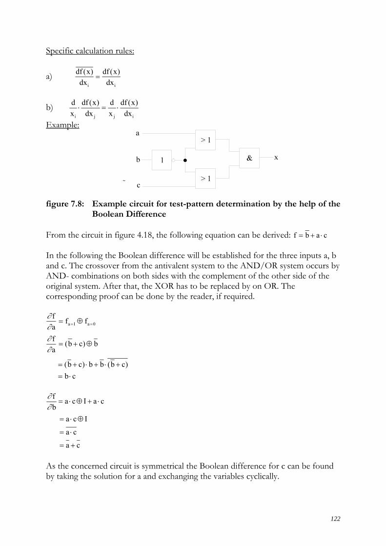
122
Specific calculation rules:
a) df (x)dx
df (x)dxi i
=
b) d
xdf (x)dx
dx
df (x)dxi j j i
⋅ = ⋅
Example:
figure 7.8: Example circuit for test-pattern determination by the help of the
Boolean Difference From the circuit in figure 4.18, the following equation can be derived: f b a c= + ⋅ In the following the Boolean difference will be established for the three inputs a, b and c. The crossover from the antivalent system to the AND/OR system occurs by AND- combinations on both sides with the complement of the other side of the original system. After that, the XOR has to be replaced by on OR. The corresponding proof can be done by the reader, if required. ∂∂∂∂
fa
f f
fa
(b c) b
(b c) b b (b c)b c
a I a 0= ⊕
= + ⊕
= + ⋅ + ⋅ += ⋅
= =
∂∂
fb
a c I a c
a c I
a c
a c
= ⋅ ⊕ + ⋅
= ⋅ ⊕
= ⋅
= +
As the concerned circuit is symmetrical the Boolean difference for c can be found by taking the solution for a and exchanging the variables cyclically.

123
∂∂
fc
a b= ⋅
Every solution ∂ ∂f / x Ii = with xi ={a,b,c} describes a signal path from xi to f. To accomplish a test for a specific error, xi additionally has to be switched to the inverse value of the fault. A test for a stuck-at-0 fault at the primary input a thus is: T a f
aa / sa0 = ⋅∂∂
from ∂∂
fa
I= we get b = I and c = I
from a/sa0 we get a = I From this the stimuli for the inputs have to be a = I, b = I, c = I for the according test-pattern. By examining all boolean differences, the test-patterns for all possible stuck-at errors at the primary inputs can be established. c b a c b a c b a c b a Ta/sa0 I I I Tb/sa0 0 I 0 Tb/saI 0 0 0 Tc/sa0 I I I Ta/saI I I 0 I I 0 I 0 0 Tc/saI 0 I I 0 I I 0 0 I
Table 7.3 The found set is the complete test-pattern set which can be further reduced for application. Minimum test-pattern sets: A minimum test-pattern set has to include at least one test for every possible fault. In the above example the test for s-a-0 at a is same as for stuck-at-0 at c and also s-a-I at c tests s-a-0 at b. Additionally one of the three patterns of s-a-I at b has to be chosen. The so found set can be used for a functional test. a) Functional test (Go / No go Test):
Test fault 0 0 0 ===> {Tb/saI } 0 I I ===> {T , Tc/saI b/sa0}I I 0 ===> {T , Ta/saI b/sa0}I I I ===> {T , Ta/sa0 c/sa0}
Table 7.4

124
There are 4 resulting patterns, thus the set is relatively small but only gives small possibilities for further investigations or diagnostics. b) Diagnostics When taking into account “maximum differentiability of faults” while selecting test-patterns from the complete set, a diagnostic test can be evaluated. This test is interesting especially for precise analysis, e.g. for repairing or systematic improvement of production processes, as it possibly indicates the location of a fault. The method for setting up a diagnostic test is: 1. List all tests with unique fault assignment assignment. 2. Selection of test-patterns from the set such that preferably only additional
tests are listet. By selecting different patterns for errors at b it can be offered to find the location of the error, additionally to just recognizing an error. The selected patterns here are:
Test Error I I I ===> {
T , Ta/sa0 c/sa0} I I 0 ===> Ta/saI 0 I I ===> Tc/saI 0 I 0 ===> Tb/sa0 0 0 I ===> Tb/saI
Table 7.5
7.5.2 Path-sensitization
When looking back at the boolean difference as a method for test-pattern generation it can be seen that it always provides all patterns for a fault and thus also all paths. The boolean difference also is a very effording method. In this chapter it is shown how to develop a path for only a single fault. This method is very general and is used in the contruction of various tools for test generation. The first question is: How can a sensititive path be created? Thereby a sensitive path should be defined in a way such that an error at the input of a circuit can be observed at the output. As an example an AND- and an OR- gate are considered. Here the variable a is considered switchable and b is a signal-variable.
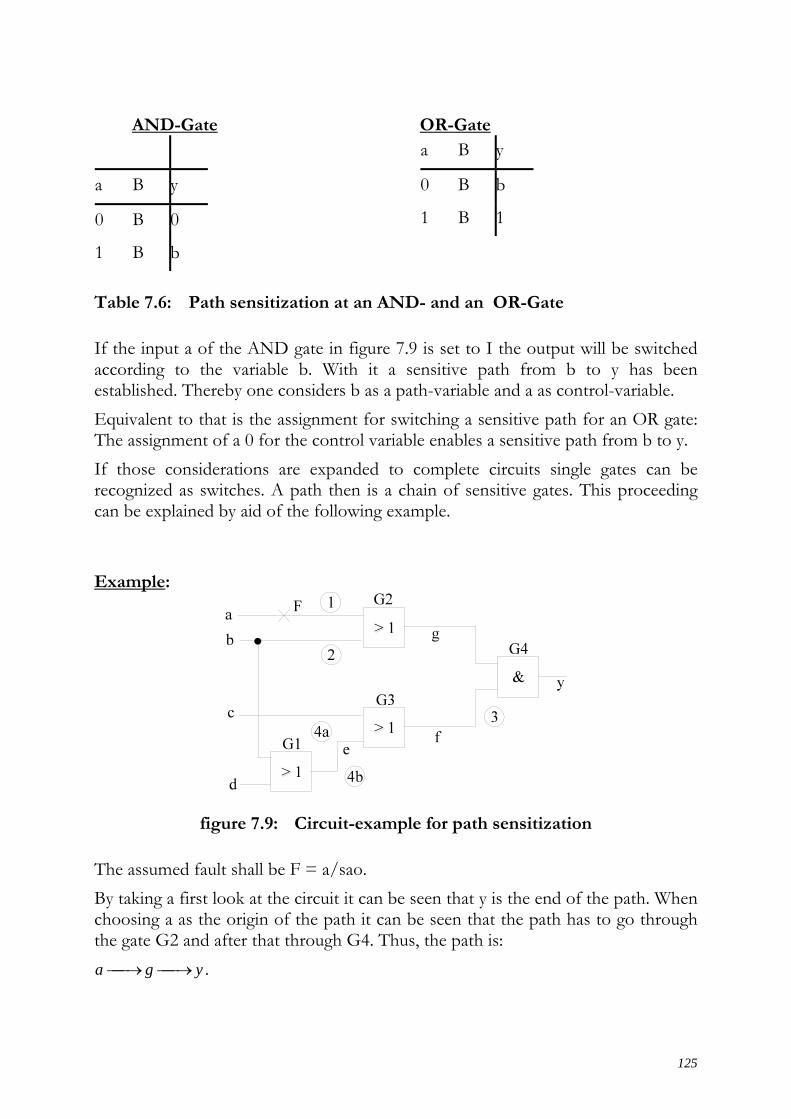
125
AND-Gate
a B y
0 B 0
1 B b
OR-Gate a B y
0 B b
1 B 1
Table 7.6: Path sensitization at an AND- and an OR-Gate If the input a of the AND gate in figure 7.9 is set to I the output will be switched according to the variable b. With it a sensitive path from b to y has been established. Thereby one considers b as a path-variable and a as control-variable. Equivalent to that is the assignment for switching a sensitive path for an OR gate: The assignment of a 0 for the control variable enables a sensitive path from b to y. If those considerations are expanded to complete circuits single gates can be recognized as switches. A path then is a chain of sensitive gates. This proceeding can be explained by aid of the following example. Example:
figure 7.9: Circuit-example for path sensitization The assumed fault shall be F = a/sao. By taking a first look at the circuit it can be seen that y is the end of the path. When choosing a as the origin of the path it can be seen that the path has to go through the gate G2 and after that through G4. Thus, the path is: a g y⎯→⎯ ⎯→⎯ .

126
The following 5 steps establish a sensitive path from a to y. The single steps are indicated by encircled numbers in figure 7.9.
Steps PI internal PO Action a b c d e f g y 1. I Error-activation by I at
Node a 2. I 0 I Sensitize G2 (OR- Gate), by
0 at b 3. I 0 I I I sensitize G4 (AND-Gate) by
I at f Requirement f=I has to be fulfilled by backtracing to the PIs 4a) I 0 I I I I Justify f = I e.gg by c = I 5a) I 0 I X X I I I complete assignment of the
nodes for the test of a/sao
Table 7.7: Switching of a critical path from a -->y for the circuit in figure 7.9
Comparison of this figure with the circuit shows that the step 4a) doesn’t show a unique possibility for a jusification of f = I. Alternatively e = I could have been chosen. Table 7.8 takes this alternative and continues with the sensitization from that point. Steps A b C d e f g y Action 4b) I 0 I I I I Alternative justification for f
= I 5b) I 0
I X I I I I I Contradiction possible here
if e.g. b=I is demanded Table 7.8: Alternative proceeding for justification of the critical path a ---> y Apart from the fault F = a/sa0 and respectively F = a/sa1 the following are recognized, too: 1. all signal-values complementary to the assignment of the path 2. Possibly additional faults caused by the justification assignment (This
especially holds at circuits with multiple POs, as additional errors are oberservable at the other outputs.)
a g y⎯→⎯ ⎯→⎯ is a free path. I.e. that the path is sensitive to both error types a/sa0 and a/sa1 in the same way.

127
Now we consider an error at b in the circuit of Figure 5.1. As b is used to control the other gates in the circuit and at the same time a path b g y⎯→⎯ ⎯→⎯ exists, it can lead to only one fault to be recognized, as b is not only the startvalue of the path, but also control-variable for sensitizing of the path. In the following we see the general setps, necessary for path sensitizing. 1. Elementary operations a) Choose type and position of the fault => Demand for the complementary
signal at the position of error for the given type of fault. b) Allocate all remaining inputs such that a sensitive path through the following
gate is established. c) Justify all control assignments. 2. Procedure (offers two alternatives) d1) d2)
Choose by a) Choose by a) Assign by b) Assign by b) Justify by c) when demanded all gates along the path
Justify (by c) => Path assembly starting from PI => path demand complete (Wojtkoviak uses this variant) Assembly (starting from PI) from P0 e) Choice of a path at the fan-out node f) Choice of an input when justifying via dominating value (0 at (N)AND 1 at
(N)OR ) Caused by the possibility to choose, this method is controlled heuristically.
(Heuristic = reasonable suggestion). for e) Try to choose longest path, as probably a lot of additional faults are
recognized. for f) Try to choose shortest path, as the probability for contradictions is rather
small for the justification. Often only a trivial-heuristic is utilized: „Choose all inputs x1...xn in a sequence“. Additionally the inputs can be rated by measurement values from testability analysis or structural analysis.

128
figure 7.10: path sensitization (without backtracing)