novel modulation technique for radio-over-fiber systems
TRANSCRIPT
Novel Modulation Technique
for Radio-over-Fiber Systems
Minhong Zhou
A Thesis
in
The Department
of
Electrical and Computer Engineering
Presented in Partial Fulfillment of the Requirements
for the Degree of Master of Applied Science (Electrical and Computer Engineering) at
Concordia University
Montreal, Quebec, Canada
August, 2007
© Minhong Zhou, 2007

1*1 Library and Archives Canada
Published Heritage Branch
395 Wellington Street Ottawa ON K1A0N4 Canada
Bibliotheque et Archives Canada
Direction du Patrimoine de I'edition
395, rue Wellington Ottawa ON K1A0N4 Canada
Your file Votre reference ISBN: 978-0-494-40900-8 Our file Notre reference ISBN: 978-0-494-40900-8
NOTICE: The author has granted a nonexclusive license allowing Library and Archives Canada to reproduce, publish, archive, preserve, conserve, communicate to the public by telecommunication or on the Internet, loan, distribute and sell theses worldwide, for commercial or noncommercial purposes, in microform, paper, electronic and/or any other formats.
AVIS: L'auteur a accorde une licence non exclusive permettant a la Bibliotheque et Archives Canada de reproduire, publier, archiver, sauvegarder, conserver, transmettre au public par telecommunication ou par Plntemet, prefer, distribuer et vendre des theses partout dans le monde, a des fins commerciales ou autres, sur support microforme, papier, electronique et/ou autres formats.
The author retains copyright ownership and moral rights in this thesis. Neither the thesis nor substantial extracts from it may be printed or otherwise reproduced without the author's permission.
L'auteur conserve la propriete du droit d'auteur et des droits moraux qui protege cette these. Ni la these ni des extraits substantiels de celle-ci ne doivent etre imprimes ou autrement reproduits sans son autorisation.
In compliance with the Canadian Privacy Act some supporting forms may have been removed from this thesis.
Conformement a la loi canadienne sur la protection de la vie privee, quelques formulaires secondaires ont ete enleves de cette these.
While these forms may be included in the document page count, their removal does not represent any loss of content from the thesis.
Canada
Bien que ces formulaires aient inclus dans la pagination, il n'y aura aucun contenu manquant.

Abstract
Novel modulation technique for radio-over-fiber systems
Minhong Zhou
Fiber-optic communications have been widely used and deployed across the globe. As
the bottom structure of optical communication networks, optical access networks connect
a central office with base stations in local networks. Falling into the category of optical
access networks, Radio-over-fiber (RoF) technique offers the future access solutions for
high speed and capacity wireless communication. RoF technique uses optical fiber to
distribute high frequency RF signals between central office and base stations. At present,
two main RoF modulation techniques exist, optical double sideband modulation (ODSB)
and optical single sideband modulation (OSSB). OSSB is preferred due to robustness to
chromatic dispersion but ODSB not. In typical OSSB, modulation efficiency i.e. optical
carrier-to-sideband power ratio (OCSR) is merely determined by RF amplitude.
Large/small RF signals can lead to small/large OCSR and large/small nonlinear
distortions. OCSR directly determines RF output power. The goal of new modulation
technique is to improve modulation efficiency by suppressing OCSR and keep nonlinear
distortions low.
In this work, we propose and analyze a novel modulation technique, consisting of two
parallel dual-electrode Mach-Zehnder modulators (MZMs). With this proposed
modulation technique, OSSB with adjustable OCSR can be achieved by adjusting two
iii
DC biases of the MZMs. We first make theoretical analysis and then finish simulation
verification. Their results agree with each other very well. Both of them show that RF
output power can be greatly improved by adjusting OCSR. Furthermore, the optimum
OCSR is OdB when one RF is applied to modulation optical carrier and it is 3dB in the
case of two RF signals.
IV

Acknowledge
I wish to express my sincere appreciation to my supervisor Dr. John Xiupu Zhang for
his help and support during my study at Concordia. His insight, expertise and wealth of
knowledge are invaluable to me. Without his help, 1 could not finish this study.
I would like to thank my friends of Li Zhu, Shaofeng An, Chengwei Gu and Xujun Li
for their English correction of this thesis.
Finally, I would like to thank my family, especially my girlfriend Quan Zhang, for all
the love and support from them.
V

CONTENTS
Chapter 1 Introduction 1
1.1 Fiber-optic communication 1
1.2 Radio over fiber (RoF) 5
1.2.1 What is RoF 5
1.2.2 Benefits of RoF technique 8
1.2.3 Techniques for generating and transporting RF signals over optical fiber 12
1.2.4 Limitations of RoF technique 14
1.3 Literature review and motivation 16
1.4 Organization of the thesis 19
Chapter 2 Proposed modulation technique and theoretical analysis 20
2.1 Principle of proposed modulation technique 21
2.2 Theoretical analysis of proposed modulation technique 26
2.2.1 Proposed modulator driven by one RF signal 26
2.2.2 Proposed modulator driven by two RF signals 31
Chapter 3 Simulation and comparison with theoretical analysis 37
3.1 Proposed modulator driven by one RF signal 39
3.1.1 Optical single sideband modulation with adjustable optical carrier-to-sideband
ratio 39
vi

3.1.2 Impact of 1DCOP and 2DCOP on OCSR 43
3.1.3 Impact of OCSR on RF output power and SNR 50
3.1.4 Phase sensitivity of proposed modulation technique 59
3.2 Proposed modulator driven by two RF signals 61
3.2.1 Impact of lDCOPand 2DCOP on OCSR 62
3.2.2 Impact of OCSR on RF output power and IM3 66
3.2.3 Impact of frequencies of RF signals on SNR 78
Chapter 4 Conclusions and future work 82
4.1 Major contribution 82
4.2 Future work 83
References 84
vii

List of figures
Fig. 1.1 Transmission attenuation losses versus wavelength 2
Fig. 1.2 Optical networks structure 3
Fig. 1.3 Generating RF signals by direct intensity modulation (a) of the laser; (b) using
an external modulator 13
Fig. 1.4 Sub-carrier multiplexing of mixed digital and analogue signals 14
Fig. 2.1 Schematic of improving modulation efficiency 20
Fig. 2.2 Schematic of our proposed modulation technique (one sub-carrier) 22
Fig. 2.3 Schematic of our proposed modulation technique (two sub-carriers) 25
Fig. 2.4 Schematic of the analytical model 26
Fig. 2.5 (a) Optical and (b) electrical spectra of proposed modulation 30
Fig. 2.6 (a) Optical spectra after EDFA (b) electrical spectra after photodetector 35
Fig. 3.1 Optical spectrum after EDFA under different IDCOP (a)lDCOp=0V; (b)
lDCop=1.0V;(c)lDCOp=1.4V;(d)lDCOp=2.1V 40
Fig. 3.2 RF power loss in OSSB and ODSB 43
Fig. 3.3 Impact of £, (normalized MZM bias lDCOP) on OCSR when MI=0.05 45
Fig. 3.4 Impact of ^ (normalized MZM bias 1DC0P) on OCSR when MI=0.1 46
Fig. 3.5 Impact of ^ (normalized MZM bias IDCOP) on OCSR when MI=0.2 47
Fig. 3.6 Impact of & (normalized MZM bias IDCOP) on OCSR when MI=0.5 48
Fig. 3.7 Impact of OCSR on RF output power when MI=0.05 51
viii

Fig. 3.8 Impact of OCSR on SNR when MI=0.05 52
Fig. 3.9 Impact of OCSR on RF output power when MI=0.1 53
Fig. 3.10 Impact of OCSR on SNR when MI=0.1 53
Fig. 3.11 Impact of OCSR on RF output power when MI=0.2 54
Fig. 3.12 Impact of OCSR on SNR when MI=0.2.... 55
Fig. 3.13 Impact of OCSR on RF output power when MI=0.5 56
Fig. 3.14 Impact of OCSR on SNR when MI=0.5 56
Fig. 3.15 Phase sensitivity when MI=0.05 59
Fig. 3.16 Phase sensitivity when MI=0.1 60
Fig. 3.17 Phase sensitivity when MI=0.2 60
Fig. 3.18 Phase sensitivity when MI=0.1 61
Fig. 3.19 Impact of lDCOP on OCSR when MI=0.05 63
Fig. 3.20 Impact of lDCOP on OCSR when MI=0.1 64
Fig. 3.21 Impact of lDCOP on OCSR when MI-0.2 65
Fig. 3.22 Impact of lDCOP on OCSR when MI=0.5 66
Fig. 3.23 Impact of OCSR on RF1 output power and IM3 (2fi-f2) when MI=0.05 67
Fig. 3.24 Impact of OCSR on RF2 output power and IM3 (2f2-fi) when MI=0.05 68
Fig. 3.25 Impact of OCSR on SNR when MI=0.05 68
Fig. 3.26 Impact of OCSR on RF 1 output power and IM3 (2/}-/2) when MI-0.1 70
Fig. 3.27 Impact of OCSR on RF2 output power and IM3 (2f2-fi) when MI=0.1 70
Fig. 3.28 Impact of OCSR on SNR when MI=0.1 71
ix

Fig. 3.29 Impact of OCSR on RF1 output power and IM3 {2f,-f2) when MI=0.2 72
Fig. 3.30 Impact of OCSR on RF2 output power and IM3 (2f2-fi) when MI=0.2 72
Fig. 3.31 Impact of OCSR on SNR when MI=0.2 73
Fig. 3.32 Impact of OCSR on RF1 output power and IM3 (2/,-/2) when MI=0.5 74
Fig. 3.33 Impact of OCSR on RF2 output power and IM3 (2f2-fi) when MI=0.5 75
Fig. 3.34 Impact of OCSR on SNR when MI=0.5 75
Fig. 3.35 Impact of RF1 frequency on SNR] 79
Fig. 3.36 Impact of RF2 frequency on SNR2 79
X

List of Tables
Table 1 CW laser parameters 37
Table 2 DE-MZM parameters 38
Table 3 PD parameters 39
XI

List of Acronyms and Abbreviations
RoF
MZM
DE-MZM
OCSR
MI
IMD
HD
IMD3
SNR
SCM
OSSB
ODSB
QoS
WDM
DWDM
FDM
OTDM
RF
LSB
Radio over fiber
Mach-Zehnder modulator
Dual electrode Mach-Zehnder modulator
Optical carrier-to-sideband ratio
Modulation index
Inter-modulation distortion
Harmonic distortion
Third order inter-modulation distortion
Signal-to-noise ratio
Sub-carrier modulation
Optical single sideband
Optical double sideband
Quality of service
Wavelength-division-multiplexing
Dense-wavelength-division-multiplexing
Frequency division multiplexing
Optical time division multiplexing
Radio frequency
Lower sideband
Xll

USB
WAN
MAN
LAN
PON
FTTP
FTTH
FBG
AWG
EMI
CO
BS
IM-DD
CW
NF
PD
EDFA
SBS
Upper sideband
Wide area network
Metropolitan area network
Local area network
Passive optical network
Fiber to the premises
Fiber to the home
Fiber Bragg grating
Arrayed waveguide grating
Electromagnetic interference
Central office
Base station
Intensity modulation-direct detection
Continuous wave
Noise figure
Photo detector
Erbium doped fiber amplifier
Stimulated Brillouin scattering
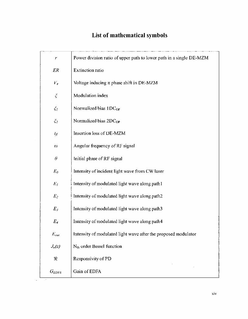
List of mathematical symbols
r
ER
V,
Z
6
6
tff
CO
e
Eo
Ei
E2
E3
E4
t^out
J„(z)
ft
GEDFA
Power division ratio of upper path to lower path in a single DE-MZM
Extinction ratio
Voltage inducing TC phase shift in DE-MZM
Modulation index
Normalized bias lDCop
Normalized bias 2DC0p
Insertion loss of DE-MZM
Angular frequency of RF signal
Initial phase of RF signal
Intensity of incident light wave from CW laser
Intensity of modulated light wave along pathl
Intensity of modulated light wave along path2
Intensity of modulated light wave along path3
Intensity of modulated light wave along path4
Intensity of modulated light wave after the proposed
N^ order Bessel function
Responsivity of PD
GainofEDFA
modulator
XIV

Chapter 1 Introduction
1.1 Fiber-optic communication
Driven by the increasing demand of internet data traffic, fiber-optic communication
system has been developed dramatically and the optical transmission links have been
widely built all over the world. The fiber communication system offers a network
infrastructure of huge information capacity and has already become the essential part of
the whole communication network. The fiber system delivers both the voice-oriented and
the data-oriented information in a very economical way, while achieving the required
quality of service (QoS).
As the crucial element of an optical signal transmission, optical fibers offer wider
available bandwidth, lower signal attenuation, and smaller signal distortion than other
sorts of wired physical media. The optical fiber can allow long transmission distance at
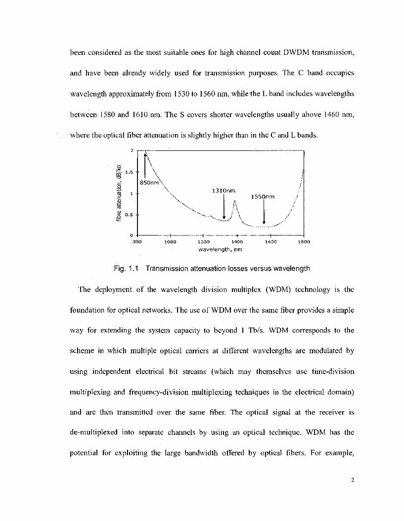
high bit rates. Fig. 1.1 shows a typical attenuation curve of a single-mode optical fiber
used today. It pictures out the relationship between the transmission attenuation loss and
the available bandwidth. As can be seen in Fig. 1.1, the transmission attenuation is
relatively low when the wavelength of fiber is about 1310 nm and 1550 nm. For instance,
at the wavelength of 1550 nm, the fiber attenuation loss is 0.2 dB/km, which is suitable.
Normally, the usable optical wavelength can be split into several wavelength bands. The
bands around the minimum attenuation region usually is referred to C and L bands, have
l
been considered as the most suitable ones for high channel count DWDM transmission,
and have been already widely used for transmission purposes. The C band occupies
wavelength approximately from 1530 to 1560 nm, while the L band includes wavelengths
between 1580 and 1610 nm. The S covers shorter wavelengths usually above 1460 nm,
where the optical fiber attenuation is slightly higher than in the C and L bands.
S
,- 1.5
3 i cr ft!
0 .5
r \
850nro ; \ 131.0nm
\
1550nm
; \
-+- -+-SS€ 120O 1400
wavelength, nm lfifl-0 1800
Fig. 1.1 Transmission attenuation losses versus wavelength
The deployment of the wavelength division multiplex (WDM) technology is the
foundation for optical networks. The use of WDM over the same fiber provides a simple
way for extending the system capacity to beyond 1 Tb/s. WDM corresponds to the
scheme in which multiple optical carriers at different wavelengths are modulated by
using independent electrical bit streams (which may themselves use time-division
multiplexing and frequency-division multiplexing techniques in the electrical domain)
and are then transmitted over the same fiber. The optical signal at the receiver is
de-multiplexed into separate channels by using an optical technique. WDM has the
potential for exploiting the large bandwidth offered by optical fibers. For example,
hundreds of 10 GB/s channels can be transmitted over the same fiber when channel
spacing is reduced to below 100GHz.
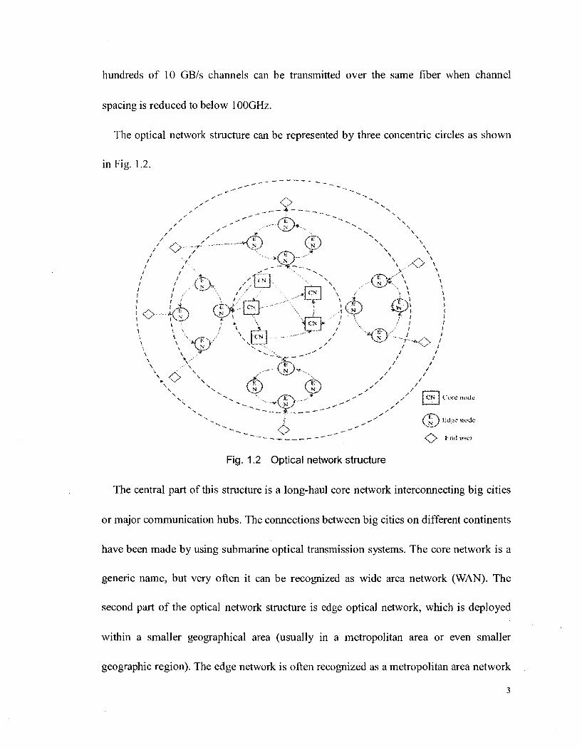
The optical network structure can be represented by three concentric circles as shown
in Fig. 1.2.
Fig. 1.2 Optical network structure
The central part of this structure is a long-haul core network interconnecting big cities
or major communication hubs. The connections between big cities on different continents
have been made by using submarine optical transmission systems. The core network is a
generic name, but very often it can be recognized as wide area network (WAN). The
second part of the optical network structure is edge optical network, which is deployed
within a smaller geographical area (usually in a metropolitan area or even smaller
geographic region). The edge network is often recognized as a metropolitan area network
3

(MAN). Finally, the access network is a peripheral part of the optical network related to
the last-mile access and bandwidth distribution to the individual end users (corporate,
government, medical, entertainment, scientific, and private). Access networks examples
include the enterprise local area networks (LAN) and a distribution network that connects
the central office location with individual users. Compared with the progress made in the
first two structures, the optical access technology is not mature and people still can
develop a lot. Basically, all of the efforts concerning researching optical access
networking focus on RoF (radio over fiber) and PON (passive optical network). RoF
mainly offers the future wireless access solution in which the radio frequency signals
propagate over the fiber. The main advantages of this technology are that it can make the
base stations or antenna stations (the corresponding definition to central office) simpler
so to simplify the installation and maintenance and can offer much wider bandwidth with
lower attenuation loss so to facilitate higher quality mobile communication service than
the conventional. The thesis proposes and develops a new modulation technique for RoF
and more details concerning RoF will be presented in the following section. Passive
Optical Networks (PON) is the leading technology being used in FTTP (Fiber to the
Premises), FTTH (Fiber to the Home) deployments. The advantages of PON over the
conventional technique are that it can offer much wider bandwidth with deeper
penetration and it needs less fiber deployment with only one port in central office.

1.2 Radio over fiber (RoF)
As a promising access technique, RoF can be applied in cellular networks, satellite
communications, video distribution systems, wireless LANs, vehicle communication and
control, phase array radar etc. Applications for RoF in cellular networks are usually split
into three types: radio coverage extension and capacity distribution and allocation. The
first case includes applications for railway and motorway tunnels, canyons, and similar
dead spot areas that because of their specific needs often do not justify the costs of
installing and operation new BS. The second case includes applications for subway
stations, exhibition grounds, airports, downtown street levels, and other densely
populated environments where the traffic requirement leads to dedicated radio channels
that need to be distributed appropriately. Both of the preceding two cases have been
practically implemented in the existing cellular networks. The third cases will be
applicable for the future 3G or 4G communication networks. As cell size of the future
cellular network decreases and frequency of RF signal increases, RoF offers the great
access solution to the future cellular communication networks.
1.2.1 What is RoF
Due to their ease of installation in comparison to fixed networks, wireless
communication has experienced tremendous growth in the last decade. However, as the
demand of high quality service like high definition video talk, internet data transferring
5

increases considerably, the capacity of the current narrowband wireless access networks
seems insufficient.
One natural way to increase capacity of wireless communication systems is to deploy
smaller cells (micro- and pico-cells) [1] [2]. This is generally difficult to achieve at
low-frequency microwave carriers, but by reducing the radiated power at the antenna, the
cell size may be reduced somewhat. Pico-cells are also easier to form inside buildings,
where the high losses induced by the building walls help to limit the cell size. Smaller
cell sizes lead to improved spectral efficiency through increased frequency reuse. But, at
the same time, smaller cell sizes mean that large numbers of base stations are needed in
order to achieve the wide coverage required for ubiquitous communication systems.
Furthermore, extensive feeder networks are needed to service the large number of base
stations. Therefore, unless the cost of the base stations and the feeder network are
significantly low, the system-wide installation and maintenance costs of such systems
would be rendered prohibitively high. This is where Radio-over-Fiber (RoF) technology
comes in. It achieves the simplification of the base stations through consolidation of radio
system functionalities at a centralized head end, which are then shared by multiple base
stations.
Another way to increase the capacity of wireless communication systems is to increase
the carrier frequencies. Higher carrier frequencies offer greater modulation bandwidth,
but may lead to increased costs of radio front-ends in the base stations. In conventional
wireless communication systems, the media for transmission channel is the air. However,
6

radio signals with high frequencies will attenuate greatly when propagating in the air.
Even the penetration ability of going through obstacles into building will also decrease
extremely. When radio signals at the frequency of 60 GHz propagate in the air, the
attenuation loss can be as large as 10-15 dB/km. In other words, if we transmit typical
radio signal at 60 GHz directly over the air, it will only be able to propagate for less than
2 km.
Radio-over-Fiber (RoF) technique entails the use of optical fiber links to distribute
radio frequency (RF) signals from a central office to base stations. In narrowband
communication systems, RF signal processing functions such as frequency up-conversion,
carrier modulation, and multiplexing, are performed at the base stations, and immediately
fed into the antenna. RoF makes it possible to centralize the RF signal processing
functions in one shared location (Central Office), and then to use optical fiber, which
offers low signal loss (0.2 dB/km for 1550 nm, and 0.5 dB/km for 1310 nm wavelengths)
to distribute the RF signals to the base stations. By so doing, base stations are simplified
significantly, as they only need to perform optoelectronic conversion and amplification
functions. The centralization of RF signal processing functions enables equipment
sharing, dynamic allocation of resources, and simplified system operation and
maintenance. These benefits can translate into major system installation and operational
savings [3], especially in wide-coverage broadband wireless communication systems,
where a high density of base stations is necessary as discussed above.
7
1.2.2 Benefits of RoF technique
Some of the advantages and benefits of the RoF technology compared with electronic
signal distribution are given below.
a. Low attenuation loss
Commercially available standard Single Mode Fibers (SMFs) made from glass (silica)
have attenuation losses below 0.2 dB/km and 0.5 dB/km in the 1550 nm and the 1310 nm
windows, respectively. We have mentioned the situation of RoF over the air above.
Obviously, it is not suitable for being the transmission medium when RF signals'
frequencies increase greatly. As another common type of transmission medium, coaxial
cables' losses are higher by three orders of magnitude at higher frequencies. For instance,
the attenuation of a V2 inch coaxial cable (RG-214) is >500 dB/km for frequencies above
5 GHz [4]. Therefore, by transmitting microwaves in the optical form, transmission
distances are increased several folds and the required transmission powers reduced
greatly.
b. Large bandwidth
Optical libers offer enormous bandwidth. There are three main transmission windows,
which offer low attenuation, namely the 850 nm, 1310 nm, and 1550 nm wavelengths.
For a single SMF optical fiber, the combined bandwidth of the three windows is in the
excess of 50 THz. However, today's state-of-the-art commercial systems utilize only a
fraction of this capacity (1.6 THz). But developments to exploit more optical capacity per
8

single fiber are still continuing. The main driving factors towards unlocking more and
more bandwidth out of the optical fiber include the availability of low dispersion (or
dispersion shifted) fiber, the Erbium Doped Fiber Amplifier (EDFA) for the 1550 nm
window, and the use of advanced multiplex techniques namely Optical Time Division
Multiplexing (OTDM) in combination with Dense Wavelength Division Multiplexing
(DWDM) techniques. The enormous bandwidth offered by optical fibers has other
benefits apart from the high capacity for transmitting microwave signals. The high optical
bandwidth enables high speed signal processing that may be more difficult or impossible
to do in electronic systems. In other words, some of the demanding microwave functions
such as filtering, mixing, up- and down-conversion, can be implemented in the optical
domain [5]. For instance, mm-wave filtering can be achieved by first converting the
electrical signal to be filtered into an optical signal, then performing the filtering by using
optical components such as the Mach Zehnder Interferometer (MZI) or Fiber Bragg
Gratings (FBG), and then converting the filtered signal back into electrical form.
Furthermore, processing in the optical domain makes it possible to use cheaper low
bandwidth optical components such as laser diodes and modulators, and still be able to
handle high bandwidth signals [6]. The utilization of the enormous bandwidth offered by
optical fibers is severely hampered by the limitation in bandwidth of electronic systems,
which are the primary sources and receivers of transmission data. This problem is
referred to as the "electronic bottleneck. The solution around the electronic bottleneck
lies in effective multiplexing. OTDM and DWDM techniques mentioned above are used
9
in digital optical systems. In analogue optical systems including RoF technology,
Sub-Carrier Multiplexing (SCM) is used to increase optical fiber bandwidth utilization. In
SCM, several microwave sub carriers, which are modulated with digital or analogue data,
are combined and used to modulate the optical signal, which is then carried on a single
fiber [7], [8]. This makes RoF systems cost-effective.
c. Immunity to radio frequency interference
Immunity to Electromagnetic Interference (EMI) is a very attractive property of optical
fiber communications, especially for microwave transmission. This is so because signals
are transmitted in the form of light through the fiber. Because of this immunity, fiber
cables are preferred even for short connections at mm-waves. Related to EMI immunity
is the immunity to eavesdropping, which is an important characteristic of optical fiber
communications, as it provides privacy and security.
d. Easy installation and maintenance
In RoF systems, complex and expensive equipment is kept in central office, thereby
making the BSs simpler. For instance, most RoF techniques eliminate the need for a LO
and related equipment at the BSs. In such cases a photo detector, an RF amplifier, and an
antenna make up the BS. Modulation and switching equipment is kept in the central
office and is shared by several BSs. This arrangement leads to smaller and lighter BSs,
effectively reducing system installation and maintenance costs. Easy installation and low
maintenance costs of BSs are very important requirements for mm-wave systems,
because of the large numbers of the required BSs.
10

e. Reduced power consumption
Reduced power consumption is a consequence of having simple BSs with reduced
equipment. Most of the complex equipment is kept in the central office. In some
applications, the BSs are operated in passive mode. For instance, some 5 GHz
Fiber-Radio systems employing pico-cells can have the BSs operate in passive mode [9].
Reduced power consumption at the RAU is significant considering that BSs are
sometimes placed in remote locations not fed by the power grid.
f. Dynamic resource allocation
Since the switching, modulation, and other RF functions are performed at a central
office, it is possible to allocate capacity dynamically. For instance in a RoF distribution
system for GSM traffic, more capacity can be allocated to an area (e.g. shopping mall)
during peak times and then re-allocated to other areas when off-peak (e.g. to populated
residential areas in the evenings). This can be achieved by allocating optical wavelengths
through Wavelength Division Multiplexing (WDM) as need arises [10]. Allocating
capacity dynamically as need for it arises obviates the requirement for allocating
permanent capacity, which would be a waste of resources in cases where traffic loads
vary frequently and by large margins [3]. Furthermore, having the central office
facilitates the consolidation of other signal processing functions such as mobility
functions, and macro diversity transmission [10].

1.2.3 Techniques for generating and transporting RF signals over optical
fiber
There are several optical techniques for generating and transporting microwave signals
over fiber. RoF techniques may be classified in terms of the underlying
modulation/detection principles employed. In that case, the techniques may be grouped
into three categories, namely Intensity Modulation- Direct Detection (IM-DD), Remote
Heterodyne Detection (RHD) [11], and harmonic up-conversion techniques. IM-DD is
the simplest method and also the most widely used at present. Not only the modulation
techniques discussed below but also our modulation technique belongs to this category.
SCM is another principal technique which is used extremely widely in RoF systems. This
technique can help RoF make full use of the sufficiency optical fiber bandwidth.
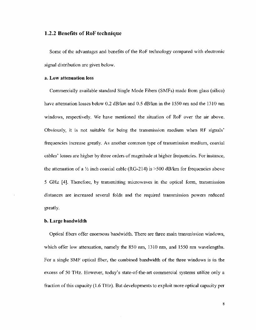
a. Some techniques for generating RF signals over optical fiber
IM-DD is simply to directly modulate the intensity of the light source with the RF
signal itself and then to use direct detection at the photo detector to recover the RF signal.
There are two ways of modulating the light source. One way is to let the RF signal
directly modulate the laser diode's current. The second option is to operate the laser in
continuous wave (CW) mode and then use an external modulator such as the
Mach-Zehnder Modulator (MZM), to modulate the intensity of the light. The two options
are shown in Fig. 1.3. In both cases, the modulating signal is the actual RF signal to be
distributed. The RF signal must be appropriately pre-modulated with data prior to
12
transmission.
Transmitter 1
RF Signal • 7k J
Bias
(a)
Transmitter 2
RF Signal
¥ -> MZM
- A ^ A '9 Bias
(b)
Fig. 1.3 Generating RF signals by direct intensity modulation (a) of a laser; (b) using an
external modulator
Evidently, direct intensity modulation is, in principle, even simpler than external
modulation. So it is used everywhere that it can be used. One limiting phenomenon to its
use is the modulation bandwidth of the laser. Relatively simple lasers can be modulated
to frequencies of several giga-hertz, say 5-10 GHz. That is why at higher microwave
frequencies, say, above 10 GHz, external modulation rather than direct modulation is
applied.
b. Subcarrier modulation in RoF systems
Subcarrier Modulation (SCM) is a maturing, simple and cost effective approach for
exploiting optical fiber bandwidth in analogue optical communication systems in general
and in RoF systems in particular. In SCM, multiple RF signals (the sub-carriers) is used
to modulate an optical carrier at the transmitter's side. In this thesis, maximally two
sub-carriers are multiplexed to help us to investigate how SCM influences the system's
performance. Fig. 1.4 illustrates what SCM is.
13

Channel 1 {e,j, digital data)
Channel 2 (e.g. analog data - video)
V
iJnidhr /SCI
Ha
Atnp
Ju l t /f\ rSi
Fig. 1.4 Sub-carrier modulation of mixed digital and analogue signals
To multiplex multiple channels to one optical carrier, multiple sub-carriers are first
combined and then used to modulate the optical carrier as shown in Fig. 1.4. At the
receiver's side the sub-carriers are recovered through direct detection and then radiated.
Different modulation schemes may be used on separate sub-carriers. One sub-carrier may
carry digital data, while another may be modulated with an analogue signal such as video
or telephone traffic. In this way, SCM supports the multiplexing of various kinds of
mixed mode broadband data. Modulation of the optical carrier may be achieved by either
directly modulating the laser, or by using external modulators such as the MZM.
1.2.4 Limitations of RoF technique
Since RoF involves analogue modulation, and detection of light, it is fundamentally an
analogue transmission system. Therefore, signal impairments such as noise and distortion,
which are important in analogue communication systems, are important in RoF systems
as well. These impairments tend to limit the receiver's sensibility and Noise Figure (NF)
14
of the RoF links.
Although there are a lot of sources of interference like shot noise, thermal noise,
chromatic dispersion, nonlinear distortion due to analogue nonlinear modulation is the
dominant among all the harmful factors. Let's take an example for the systems in which
MZM is used. MZM has a squared cosine transfer function in power. In other word, it has
a nonlinear transfer function. When RF signals are applied to modulate the optical carrier
in MZM, nonlinear distortions including harmonics distortions (HDs) and
inter-modulation distortions (IMDs) will generate. Basically, HDs mainly depends on MI.
The increase of MI will lead to that the modulation will happen in the region with more
serious nonlinearity so the intensities of HDs will become larger and larger. Concerning
IMDs, it is principally determined by MI and the number of RF carriers. As MI increases,
the intensities of IMDs also will become more and more serious. Every RF sub-carrier
can inter-modulate with each other. Therefore, as multiple like two or more RF
sub-carriers are used to modulate the optical carrier, this can cause more happening of
IMDs.
Theoretically, there will be unlimited number of high order optical spectrum
components including HDs and IMDs after light wave modulated by RF signals. Due to
the limited bandwidth of the optical equipments like Multiplexer, EDFA, Photodetector,
etc, the high order like larger than three optical spectrum components will be filtered out
by those optical equipments. Therefore, those low order nonlinear distortions make great
contribution to degrade the system's performance. Compared with other low order
15

nonlinear distortions, the third order IMDs (IM3) is the most difficult to be filtered out by
optical filters because they are very close to the fundamental spectrum component. IM3
may bring devastating impact on the receiver's sensitivity if we can't handle this very
well.
1.3 Literature review and motivation
At present, the most commonly used modulation schemes in the external intensity
modulation category are optical double sideband modulation (ODSB) and optical single
sideband modulation (OSSB). Generally, ODSB can be realized by employing MZM. In
an ODSB system, the transmission and distribution of the millimeter-wave radio signal to
and from base stations (BS) is susceptible to chromatic dispersion, which seriously
degrades the transmission distance [12]-[14]. Contrastly, by using OSSB scheme, the
degradation of the transmission distance can be effectively restrained [15]-[18]. Typical
OSSB is generated by employing a dual-electrode Mach-Zehnder modulator (DE-MZM)
[19]. When we choose the millimeter RF signal of large amplitude to modulate the optical
carrier in DE-MZM, considerable harmful nonlinear distortions, i.e. HDs and IMDs, will
be generated in the system due to the analogue modulation process of DE-MZM.
However, when we choose the millimeter RF signals of small amplitude to modulate the
optical carrier, very low modulation efficiency will be produced [15]. For instance, the
power of the optically modulated millimeter wave sideband can be over 20 dB lower than
that of the optical carrier. To improve the performance of RoF transmission and signal
16

processing systems, the optical power of mm-wave are increased by starting with the high
power light sources and utilizing the optical amplifiers [21]. However, these methods also
increase the average optical power to the photo detector (PD) simultaneously. The high
power on high-frequency PD's can cause the harmonic distortion, the response reduction,
and the damage to the receiver due to the extremely large optical power incident on the
optical detector [19] [20] [21]. Besides, the low modulation efficiency also causes the
waste of the system resource. The optical power of mm-wave sideband is still much
lower than that of optical carrier, which means the optical signal power transmitted from
modulator contains a limited portion of RF sideband with useful information but a huge
portion of optical carrier with no information.
So far, suppressing the main optical carrier has become a popular way to improve the
modulation efficiency. Lots of techniques concerned have been proposed and
demonstrated, e.g. Brillouin [22], external optical filtering [19] [20] [21] and optical
attenuation [23]. However, all these techniques have one common disadvantage, which is
the increasing complexity of RoF system. In [22], the author mainly made use of
Stimulated Brillouin Scattering (SBS) mechanism in which an optical pump was
necessary to realize the SBS. External optical filters are the components to remove the
excessive power of optical carriers [19] [20]. In [21], Fiber Bragg Grating (FBG) acts like
an external filter and its values of reflectivity are adjusted to determine the degree of
suppressing optical carrier. In [23], arrayed waveguide grating (AWG) is utilized to
attenuate the optical carrier. Besides the complexity and inconvenience caused by extra
17

optical or electrical components, other harmful factors also degrade the performance of
the RoF system. In the case of SBS, the process was relatively unstable and noisy [22].
Concerning the external optical filter, it may introduce distortions into the RF signal [22].
Thus all of the techniques mentioned above are not perfectly effective for suppressing the
main optical carrier. Recently, a distinct way to suppress the optical carrier is proposed by
using a low biased MZM [24]. This method suppresses the optical carrier enormously by
adjusting DC bias and is effective to obtain a large range of optical carrier-to-sideband
ratio (OCSR) without utilizing other optical or electrical components, where OCSR of an
optically modulated mm-wave signal is defined as the ratio of the power of optical carrier
to that of the first-order sideband. Nevertheless, the disadvantage of this technique is that
the format of modulated optical signal is ODSB, which is extremely vulnerable to
chromatic dispersion degrading the performance of RoF system considerably.
In order to overcome the disadvantage referred above, we get a good motivation to
develop and investigate a new modulation technique, in which OCSR should be
adjustable conveniently and OSSB optical signal should be generated to conquer the
chromatic dispersion simultaneously. Furthermore, the optimum OCSR for maximizing
the transmission performance in fiber-radio link is 0 dB when one RF signal is used to
modulate optical carrier. Therefore, not only making the OCSR adjustable, we also plan
to realize the optimum OCSR in our modulation technique. In [21], the analysis of the
optimum OCSR with one RF signal has been presented. In this thesis, we investigate the
optimum value of the OCSR when applying two RF signals. Two RF signals
18
inter-modulate with each other while the signals are modulating the optical carrier. The
investigation is also made to show how our modulation technique affects the third order
inter-modulation (IM3), which is most detrimental nonlinear distortion to the
performance of system.
1.4 Organization of the thesis
Chapter 1 is the introduction and background section. The basic theories of optical
communication and radio-over-fiber are presented. A detailed review of current
modulation techniques is also given in this chapter.
In Chapter 2, a novel modulation technique to improve the performance of the system
is proposed and the principle is explained. Some parameters, which are crucial to the new
modulation technique, are analyzed in detail. We also establish the analytical model of
the system in which the new modulation technique is applied. Several key criteria to
evaluate the performance of system are quantified by accurate expressions.
In Chapter 3, some simulations are presented to verify the theory of the proposed
modulation technique.
Chapter 4 describes the conclusions and future work.
19

Chapter 2 Proposed modulation technique and theoretical
analysis
In this chapter, our modulation technique is proposed and the theoretical analysis is
also presented. The goal of our proposed technique is to improve the modulation
efficiency which is the crucial parameter to influence the performance of fiber-radio link.
Intuitively, the goal is illustrated in Fig. 2.1.
Optical carrier - * Optical carrier
* -o n 73
Optical carrier € 3 O o 73
RF sideband
(a)
RF sideband
(b)
RF sideband
(c)
Fig. 2.1 Schematic of improving modulation efficiency
Fig. 2.1 schematically shows how modulation efficiency is improved by suppressing
optical carrier. Fig. 2.1 (a) represents the relative positions of the optical carrier and the
RF sideband before the optical carrier gets suppressed. It is obvious that the OCSR is
tremendously large and the modulation efficiency is considerably low. Fig. 2.1 (b)
displays the situation after the optical carrier is suppressed to a certain extent, where the
OCSR is decreased by a certain obvious level and the modulation efficiency is highly
improved. Fig. 2.1 (c) exhibits the optimum OCSR after the optical carrier is further
suppressed. The optimum OCSR in Fig. 2.1 (c) doesn't indicate the actual value of the
20

optimum OCSR, which practically may be smaller or larger. For instance, the optimum
OCSR in [21] is 0 dB. However, all the investigation was developed in the situation of
one RF signal. In this thesis, we investigate whether the optimum OCSR, 0 dB, can be
realized by employing our modulation technique. Furthermore, we also make effort to
find out the optimum OCSR in the situation of two RF signals.
2.1 Principle of proposed modulation technique
In our modulation technique, dual electrode Mach-Zehnder modulator (DE-MZM) is
one of the vital components. It is fabricated by LiNb03 material. Two Titanium-diffused
LiNb03 waveguides form two paths of a MZM interferometer. The refractive index of
LiNb03 can be changed by applying an external voltage. That implies when light waves
go through the paths, their phase will be shifted by the value determined by the refractive
index. If the external voltage is from a DC bias, the phase of light wave will be shifted by
a constant. If the external voltage is from a RF signal, the phase of light wave will vary
according to the amplitude changing of RF signal. After running through the respective
waveguides, the two paths of optical signals are combined together to interfere with each
other. The final optical signal after interference depends on the phases of the optical
signals from two paths. For instance, in the absence of external voltage, the optical fields
in the two paths of the MZM interferometer experience identical phase shift and interfere
constructively. The additional phase shift introduced in one of the arms through
voltage-induced index changes destroys the constructive nature of the interference and
21
reduce the transmitted intensity.
When one RF signal is applied to modulate optical carrier, the principle of the
modulation process is illustrated in Fig. 2.2.
CW Laser.
Branch2
1DCOP
I path!
MZM1 path2
I T RF1 1DCRF
2DC0P path3
MZM2 path4
RF2 -2 2DCRF
90° phase shift
bellow
Fig. 2.2 Schematic of our proposed modulation technique (one sub-carrier)
From the left side to right side in Fig. 2.2, the light wave from laser is equally split into
two branches. The upper one is identified as Branch 1 while the lower one is named by
Branch2. Then, the optical carriers in the two branches are coupled into two DE-MZMs,
the essential components of our modulation technique. The DE-MZM along Branch 1 is
identified as MZM1 while the one associated with Branch2 is named by MZM2. Inside
each MZM two paths, upper one and lower one, are designed. The upper ones of MZM1
and MZM2 are named by pathl and path3 separately. The lower ones of MZM1 and
MZM2 are identified as path2 and path4. Three inputs are connected onto each MZM,
thus for the parallel DE-MZMs, six inputs with the name of RF], RF2, 1DCRF, 2DCRF,
IDCQP and 2 DCQP are designed. Consequently, six inputs are grouped into three pairs, i.e.
22
RF pair, DCRF pair, and DCOP pair. The RF pair consisting of RFi and RF2is reserved for
the input RF signals, which have a 90° phase discrepancy. The DCRF pair consisting of
IDCRF and 2DCRF is connected to two DC biases which are set to the quadrature point.
The DC0p pair consisting of lDC0p and 2DCopis for two other DC biases, whose values
need to be critically evaluated for the optimal OCSR and the optimum effect of
modulation.
As introduced above, the light wave from CW laser is equally split into Branchel and
Branch2, and then respectively coupled into MZM1 and MZM2 at the same time, which
means that the optical carrier is split into Pathl, Path2, Path3 and Path4. The intensities
of the light wave along Branchl and Branch2 are identical; however, after the light wave
gets into the different paths of MZMs, the intensities along Pathl, Path2, Path3 and Path4
are different due to the extinction ratio. The extinction ratio is one of the core parameters
of MZM, which represents the difference between the upper path and lower path power
split ratio. An ideal MZM has an infinite extinction ratio, though this is not realistic in
industry. After modulated by two DC biases DCop, the two optical carriers coupled into
Pathl and Path3 are phase shifted by two independent constant values which are
determined by the values of lDCop and 2DC0p respectively. Along Path2 and Path4
driven by RF signals and the other DC biases DCRF, not only the phases the optical
carriers are shifted but also two RF sidebands (upper RF sideband and lower RF sideband)
are generated next to the optical carrier in each optical signal. The inputs of RF pair and
DCRF determine the amplitudes and the phases of both optical carrier and RF sidebands.
23

When the outputs from the four paths are combined together, the optical carriers from
different paths will interfere with each other and their individual phases determine the
final intensity of the optical carrier. Besides that, the upper RF sideband from Path2 will
interfere with that from Path4 and similarly the lower RF sideband from Path2 will also
interfere with that from Pafh4. The result of RF sideband interference also depends on
their individual phases. If we set the DCRF pair at quadrature point, either the upper RF
sideband or the lower RF sideband from Path2 will have the opposite phase against that
from Path4. In that case, either the upper RF sideband or the lower RF sideband will be
canceled. As for whether the upper one or the lower one is canceled, it depends on which
original RF signal is associated with the high biasing point. In another words, if one of
V DCRFwhich locates in the same DE-MZM with the original RF signal is biased at—5-,
lower sideband will be eliminated. Reversely, it is also correct. In all, we can choose the
proper inputs for RF pair and DCRF pair to realize OSSB at first and can also adjust the
power level of the optical carrier by sweeping the values of DCop. If we desire to
suppress optical carrier to obtain a certain OCSR, the appropriate biasing points of DCOP
need to be decided.
When two RF signals are used to modulate optical carrier, both of the two signals are
phase shifted by 90°. The original signals are combined together to be applied onto RFj
and the shifted signals onto RF2. The principle of the modulation process is illustrated as
Fig. 2.3.
24

Eo
CW Laser.
Branch 1
Branch2
1DC0P
f pathl
MZM1 path2
I I RF1 1DCRF
2DC0P
I path3
MZM2 path4
1 i RF2 2DCRF
90° phase shift
E1
r/ F,
-E*
-upper
• out
bellow
Fig. 2.3 Schematic of our proposed modulation technique (two sub-carriers)
Comparing Fig. 2.3 with Fig. 2.2, we can make conclusion that the principles are
almost the same except the number of sidebands. In Fig. 2.3, along both Path2 and Path4
totally four RF sidebands exist, which are two upper RF sidebands and two lower RF
sidebands. The processes of suppressing optical carrier and canceling either upper
sidebands or lower sidebands are the same as above. In the optical spectrum of the final
output Eouh either two upper RF sidebands or two lower RF sidebands appear. In the
thesis, the amplitudes of the two RF signals are chosen equivalent to each other so the
power intensities of RF] sidebands are identical to those of RF2 sidebands. Therefore,
OCSR for both RF signals are equivalent and we merely need one mathematical
expression to develop the analysis with reference to OCSR.
25

2.2 Theoretical analysis of proposed modulation technique
CW Laser f P
tff
Our proposed Modulator
i
^ >
EDFA
Optical Domain
1 1 1 BPr I PIN
j
Electrical Domain
i i 1 BPK 1
Power
Meter
RF signal Vm f
Electrical Domain
p,„
fc
tff
CW laser output power Optical carrier frequency Insertion loss
Vm RF signal amplitude f RF signal frequency GEDFA EDFA gain BPF Bandpass filter
Fig. 2.4 Schematic of the analytical model
Fig. 2.4 shows the schematic diagram of the analytical model to evaluate the
performance in a millimeter-wave fiber-radio link incorporating our modulation
technique. The CW laser is modeled as a single mode source of frequency fc and
optical field amplitude of EQ. The principle and configuration of our proposed modulation
technique is interpreted from above.
2.2.1 Proposed modulator driven by one RF signal
We first investigate the situation in which one optical carrier carries one sub-carrier.
V Here, IDCRF and 2DCRF are set to 0 V and — respectively. The amplitudes of the
modulated light waves along Pathl, Path2, Path3 and Path4 are Ej, E2, E3 and E4
respectively, which are represented as follows
26
F - ±J-V ' ^ z2—r tLQe
E3=±£-E0er-
E4=r^-E0e •
where tff is the insertion loss of MZM and E0 is the intensity of the incident light wave
from CW laser, r is the power division ratio of upper path to lower path in a single
(1 + rf DE-MZM and depends on Extinction Ratio ER —
J-r, VDCI and VDci are the DC
biases applied on IDCQP and 2DC0p. VK is the voltage which can induce % phase shift in
DE-MZM. Vj and V2 represent the inputs of RF signals as follows
V2 = Vmcos ujt + 9-7T
(1)
(2)
where Vm, to and 0 are the input RF signal's amplitude, angular frequency and initial
V phase respectively. We define normalized DE-MZM bias parameters as: £ = — ,
v Si „ •> S2
DC 2
After combining all the four paths together, we get E0
^ ( 0 : ji\* i J ^ e* +e 2 +re - / 'VTCOS(W/+#)
+ re 2e i— —iftrcos w/+0 2 „ ( 2) (3)
27
According to Bessel function e':coso = ^ i"Jn (z)e'"° , we can expand it as follows
*-(<)=Y£» ^•+(ss*+rJ2 •n 7 11 \ in U.7 + 0+7T I . «+] j I e \ ifc';+8+-
After simplification, it becomes
£„,(*) = *f-K p"+^"+r£ ^,(^)e" 'M + S ) ((-/)" -/2"+ l (4)
When n=0, the term corresponding to optical carrier is obtained
+En e%* +e'& +yl2rJQ(£n)e~"'
When n=l, the upper RF fundamental component E+ul is equivalent to 0. That means
the upper RF sideband is eliminated.
When n-- l , the lower RF fundamental component of RF signal is symbolized as follows
E_ul = y[TffE0rJ_x{i'K)e » ^
According to J_m (z) = ( - l)m Jm (z), E_„ = -^E^rJ, {i^)e ji+e-
It is obvious that only the lower sideband exists after modulation and OSSB is achieved.
Furthermore, optical carrier-to-sideband ratio in power is also obtained
2r2J0 (£71-) + 2 cos (£, — £2 )TT + 2rJ0 (£7r)[cos £,7r + cos £27r — sin £,7r — sin £27r] + 2 OCSR[dB] ••
41-V,2 (fr)
(5)
From (5), it is recognized that three parameters, ^, £,i, and ^2, determine the value of
OCSR. As defined above, they represent the amplitudes of RF signal, IDCOP and 2DCop.
In typical conventional OSSB system, OCSR only depends on £. Here, it is verified to
28
be feasible that our purpose of adjusting OCSR can be accomplished by sweeping t,\,
and £,2- In Chapter 3, we will show how £, L,\, and t,2 exactly affect OCSR.
An EDFA is added after the parallel DE-MZMs in order to compensate the insertion
loss of DE-MZM. The output optical signal after EDFA is
WO=£<-(>) V^ EDFA
As the optical signal is detected by an ideal PD with responsivitylft, the temporal
expression of the current can be calculated from the envelope of the incident optical
signal and expressed as follows
V (') = ^EEDFAEEDFA ^.ffG EDFAEl
2 8
e-v+ e-i& +r Y^ hp (&yip(*'+tt) (tp+i2p+i)
i(,i . if,-a , V ^ T It \ inUi+ff)(/ -\" - 2 n + l \
(6)
The optical carrier component beats with the first order component of RF signal, which
makes foremost contribution to the final desired electrical signal. Finally, RF signal after
PD can be represented as
SfiV G F2
J U # u f f i F ^ 0
-rJt (£TT) cos(u>t + 0 + £i7r--)-rJl (£TT) cos(utf + 9 + £2TT - —) +
4lr 2J0 (fTT)./, (£r) cos(urt + 6 + ^ )
(7)
In (7), there are three terms totally and the first two terms including E,\ and 2̂ displays
their influence on the final RF output power. From the discussion above, we make out t,\
29

and t,2 have a great impact on OCSR. Our purpose is to investigate how OCSR affects the
final RF output power. In Chapter 3, the detailed investigation will be presented.
The optical spectra after our proposed modulator corresponding to (4) are shown
in Fig. 2.5 (a) and the electrical spectra after photo detector corresponding to (6) are
displayed in Fig. 2.5(b).
Optical carrier
i
-2Q -Q 0
RF
]_!_
/ DC power
RF
2Q 3Q GHz J .
Q 2Q 3Q GHz
(a) (b)
Fig. 2.5 (a) Optical and (b) electrical spectra of our proposed modulation
In (a), there exist optical carrier, single sideband sub-carrier and HDs at the
frequencies of ±2UJ , 3cu and even higher order components appear after
modulation. In (b), those components are converted into electrical domain after
photo detector. When optical carrier beats with itself, a portion of DC power appears.
When optical carrier beats with other RF components, fundamental, second order,
third order and even higher order RF terms appear. This situation happens when one
optical carrier carries only one RF sub-carrier. When two RF sub-carriers are used in
our modulation, the situation changes greatly as new nonlinear components will
appear. This will be discussed in the following part. HDs may degrade the
30

transmission performance in fiber-radio links very seriously. However, we can
suppress or even filter out those terms easily by properly employing electrical filters
after PD as the frequencies of those components are distant from that of the
fundamental component. Therefore, the main noise source considered here is shot
noise, thermal noise and ASE noise from EDFA. As OCSR varies, it has little
influence on those noises. Enormous improvement of RF output power due to
optimum OCSR can lead to immense improvement of SNR.
2.2.2 Proposed modulator driven by two RF signals
In this section, we investigate the situation in which one optical carrier carries two
V sub-carriers. Here, 1DCRF and 2DCRF are still set to 0 V and — respectively.
Comparing with Section 2.2.1, what we need to do is modify (1) and (2) as follows
Vx=Vm [cos {ujxt + 0,) + cos (u2t + 02)] (8)
V —V ' 2 r m
COS TV
uj.t + 6. 1 ' 2
+ COS ir
u2t + 02~- (9)
coj and CO2 are the angular frequencies of the two input RF signals. 9\ and #2 are the initial
phases of the two input RF signals. With the same definition of £, £1 and £2, (3) becomes
Eoul{t) = ^-E[
. . i t „ \ , „ \i -i— —i&r cos Uw+ft—+cos Ly+02 — £''«>* + £''&* + r e - ' ^ [ c o s H ' + e i ) + c o s ( w 2 ' + e 2 ) ] + r e ' 2 e \ { ' ' 2j I 2 2
(10)
We use Bessel function to expand it into
31

Eou, ( 0 E0\
oc oc
m =—oc w=—oc
w——oc w=—oc
When both m and n are chosen at 0, the expression of optical carrier is obtained
/[m(uy+0,+^)+n(uy+02 + | ) - y ] (11)
£„ . n
e^+eli2*+j2rJ02fa)e~"4
When m and n are fixed at +1 and n=0 respectively, the upper sideband fundamental
component of RF1 signal E+u! is equal to 0.
When m and n are fixed at -1 and 0 respectively, the lower sideband fundamental
component of RF1 signal is as follows
-/kV + ft 7T
When m and n are fixed at 0 and +1 respectively, the upper sideband fundamental
component of RF2 signal E+u! is equal to 0.
When m and n are fixed at 0 and -1 respectively, the lower sideband fundamental
component of RF2 signal is as follows
Very evidently, the upper sideband fundamental components of both RF signals are
eliminated and only lower ones are left. OSSB are achieved. The coefficients of E„ w.
and E_u are equal to each other so it is reasonable to define OCSR of the two RF - w 2
signals by employing one mathematical expression. It is also observed that only the
coefficient of J0(£ir) is coupled into both the optical carrier component and the RF
fundamental components compared with the situation with one RF signal. The formula to
32

calculate OCSR here is completely identical to (5).
An EDFA is added after the parallel DE-MZMs in order to compensate the insertion
loss of MZMs. The output light wave after EDFA is
EEDFA ( 0 = Eou, {lHGEDFA
As the optical signal is detected by an ideal PD with responsivity 3?, the temporal
expression of the current can be calculated from the envelope of the incident optical
signal and expressed as follows
V ( ' ) = •
^EEnFAEEDFA ^f_ffG EDFAE0
e 'V_|_gfc* +
oo oc
r ^ J r+Vm^7r)jn(^7ryi-(^+»,+ .)+«(^+^+ .)i +
m——oc n—— oc
oo oc
rj2 Y:r+"Jm(fr)J„(fr)e m——oc n——x
i[m(uJlt+0i+~)+n(^2i+02+~)~]
•oc oc
/?=-oc q—~oc
oc oc r E E (-0'+V,«7r)./,(£r)e
-i[ /7(u;1<+^+-)+?(u2J+fl2+-)-2 2
P = ~OC (/ ——3C
(13)
The optical carrier beats with the first order components of the two RF signals, which
makes chief contribution to the final desired RF signals. Finally, RF1 and RF2 signal
after PD can be represented as
%/ G E
7T, -rJ0 ( W (f?0 cos(u^ + 9, + £,TT - —)
-rJ0 (£TT) J, (£r) COSO*;,/ + 0, + £2TT - - )
+V2r2 J03 (̂ TT) J, (£TT) cos(a;/ + 0, + - )
(14)
33

Jl1 HyJEDFAJ^0
7 i \ -rM&)J\ (&)cos(uJ2t + 02+ £,TT - - )
7 I \ -rJ0(fr)Ji (&)cos(u2t + 92+ £2?r - - )
+72rV03 (£TT) J, (£r) cos(a;2r + #2 + - )
(15)
Comparing (14) with (15), the expressions are almost the same except the parameters
of frequencies and initial phases. Both (14) and (15) consist of three terms which indicate
the influence of 4, 4i ar>d ki-
The optical spectra after EDFA corresponding to (11) and the electrical spectra after
PD corresponding to (13) are shown in Fig. 2.6.
Optical carrier LSB-2 LSB-1 ^
2 Q 2 - Q , 2 0 , - Q
4,
2Q,
(a)
34
C power
RF1 RF2
i iM i l O Q 2 - Q , Q , H 2 2 Q ,
(b)
Fig. 2.6 (a) Optical spectra after EDFA (b) electrical spectra after photodetector
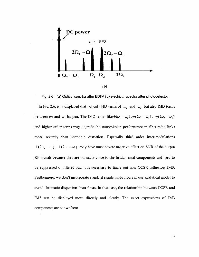
In Fig. 2.6, it is displayed that not only HD terms of u>} and UJ2 but also IMD terms
between coi and W2 happen. The IMD terms like±(a;1 — CO2),±(2LJ^ —U>2), ZL(2UJ2 —a;,)
and higher order terms may degrade the transmission performance in fiber-radio links
more severely than harmonic distortion. Especially third order inter-modulations
±(2LOX — UJ2), ±(2u2 -(j,) may have most severe negative effect on SNR of the output
RF signals because they are normally close to the fundamental components and hard to
be suppressed or filtered out. It is necessary to figure out how OCSR influences IM3.
Furthermore, we don't incorporate standard single mode fibers in our analytical model to
avoid chromatic dispersion from fibers. In that case, the relationship between OCSR and
IM3 can be displayed more directly and clearly. The exact expressions of IM3
components are shown here
/

•Jllff^JEDFA1^0
71" ^ rJAin)J2 (£TT) COS(2W f - ut + 20, - 02 + £,7r - -)
7I \ +rJ , (̂ 7r) J2 (^7r) cos^u;,/ — uJ2t + 26l—62+^2'K )
-J2r2J02 (^TT)J, (£TT)J2 (£TT) 008(20;,/ - u2t + 20, - 02 )
J U # u £ O F / l i j 0 ' 2 ^ ,
7I\ rJ, (^TT) J2 (^7r) cos(2u/2f - a?,/ + 202 - 0, + £,TT - - )
+rJ , (£TT) J2 (£TT) cos(2a;2/ - a;,/ + 202 - 0, + £2TT - - )
- V2r2702 (£TT) J, ( ^ ) 7 2 (CTT) cos(2a;2? - a;,/ + 202 - 0, - ^ )
In both (16) and (17), the first two terms include £,\ and £2> which represent I D C Q P and
2DCOP
36

Chapter 3 Simulation and comparison with theoretical
analysis
In this chapter, our proposed modulation technique is verified by computer simulations.
All the simulations are based on the platform of VPI TransmissionMaker 7.0, a
commercial software package.
The parameters of CW laser are configured as in Table 1. Emission Frequency
indicates the central emission frequency of laser and determines the wavelength of
emitted light wave. Average Power specifies the power of output light wave. Line Width
characterizes the width of the frequency interval of total emission area. Initial Phase gives
the initial phase of oscillation to generate light wave.
Table 1 CW laser parameters
Emission frequency (Hz)
Average power (w)
Line width (Hz)
Initial phase (° )
193.1xl012
l.OxlO"3
lOxlO6
0
The parameters of parallel DE-MZMs are configured as in Table 2. VnDc specifies DC
voltage required (at both split electrodes) for TX phase difference. V^RF indicates RF
voltage required (at both split electrodes) for % phase difference. Insertion Loss gives the
insertion loss of DE-MZM. Extinction Ratio characterizes the power division ratio of
upper path to lower path in a single DE-MZM.
37

Table 2 DE-MZM parameters
*W(V)
*W(V)
Insertion loss (dB)
Extinction ratio (dB)
5
5
6
15
The EDFA used in the simulation is assumed noise-free and the fixed output power
mode is chosen as its output mode. In Section 3.1.1, optical fiber with the length of 25
km is employed to investigate how chromatic dispersion influences the performance of
our system. In order to compensate the attenuation loss caused by optical fiber, the output
power of EDFA is fixed at 0 dBm. For the rest of the simulation, we choose the ideal
connection instead of single mode optic fiber between EDFA and PD in order to clearly
evaluate the improvement resulted from our modulation technique. In addition, the
optical power of incident optical signal on PD can never be larger than 0 dB, which is the
saturation value of PD. Therefore, the output power is fixed at -5 dBm when one RF
signal is applied, while the output power is -1 dBm with the input of two RF signals.
The PD parameters are configured as in Table 3. Responsivity specifies the current
generated per unit optical power. Here, we employ an ideal PD so its responsivity is 1
A/W. Dark current characterizes the current generated by the photodiode when it is not
illuminated. The ideal PD is assumed in this table. Thermal Noise represents the spectral
density of thermal noise. Shot Noise "off' indicates the noise mechanism in our
38

simulations is not considered.
Table 3 PD parameters
Responsivity (AAV)
Dark current (A)
Thermal noise (A14Hz )
Shot noise
1
0.0
10.0x10"12
Off
3.1 Proposed modulator driven by one RF signal
3.1.1 Optical single sideband modulation with adjustable optical
carrier-to-sideband ratio
The greatest attraction of our modulation technique is that not only the value of OCSR
can be adjusted, but also OSSB optical signal is obtained. In the RoF systems where
IM-DD is used, the value of OCSR represents the modulation efficiency. When OCSR is
large, it signifies considerably low modulation efficiency; when OCSR is small, it means
high modulation efficiency. Basically, modulation index (MI) determines the value of
OCSR. Large MI is able to suppress OCSR and lead to high modulation efficiency.
Reversely, when RF signal of small MI is applied to modulate light wave, OCSR is
considerably large and the modulation efficiency is low. However, the nonlinear
distortions i.e. HDs and IMDs are little in small-MI cases. If we can improve modulation
efficiency when MI is small, it will significantly improve system performance. In this
39
thesis, the goal of our modulation technique is to improve modulation efficiency and
optimize OCSR by sweeping DCop. In this section, we first show how DCOP greatly
affects OCSR, and in Section 3.1.2, we will present the detailed description regarding
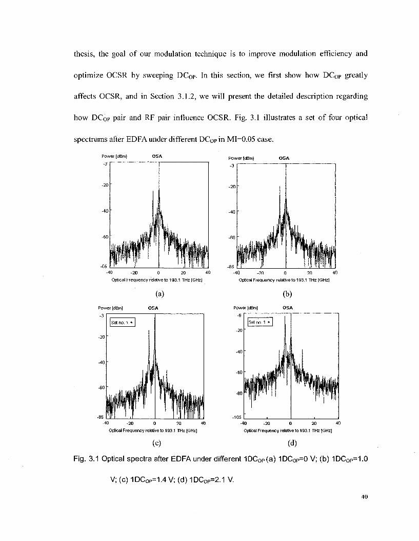
how DCOP pair and RF pair influence OCSR. Fig. 3.1 illustrates a set of four optical
spectrums after EDFA under different DCop in MI=0.05 case.
Power [dBm] OSA
-40 -20 0 20 40
Optical Frequency relative to 193.1 THz [GHz]
-40 -20 0 20 40
Optical Frequency relative to 193.1 THz [GHz]
(a)
Power [dBm) OSA
-40 -20 0 20 40
Optical Frequency relative to 193.1 THz [GHz]
-40 -20 0 20 40
Optical Frequency relative to 193.1 THz [GHz]
(c) (d)
Fig. 3.1 Optical spectra after EDFA under different 1DCOP(a) 1DCOP=0 V; (b) 1DCOp=1.0
V; (c) 1DCOP=1.4 V; (d) 1DC0P=2.1 V.
40
In Fig. 3.1, it is displayed that the upper sideband RF components are eliminated and
only the lower sideband RF components exist in all four situations. In fact, DCRF
determines whether upper sideband or lower sideband will be eliminated. Here, 1DCRF
V and 2DCRF are set to 0 V and — respectively and it leads to a lower single sideband
modulation. If we exchange their values, lower sideband RF components will be
eliminated and only upper sideband RF components will be preserved. In Fig. 3.1 (a),
IDCOP and 2DC0pare set to 0 V, 5.3 V respectively and OCSR is equal to 20 dB. To some
extent, this situation is similar to the typical optical single sideband modulation, and the
modulation efficiency is extremely low. However, the second order harmonics which
makes main contribution to the nonlinear distortion can be negligible. In Fig. 3.1 (b),
2DCOP keeps the same and lDCopis shifted to 1.0 V and it results in suppressing OCSR
to 15 dB. The second order harmonics are still awfully tiny. In Fig. 3.1 (c), lDCopis
increased to 1.4 V while 2DCOP keeps fixed, and OCSR decreases to 10 dB. In addition,
the second order harmonics become slightly noticeable. In Fig. 3.1 (d), lDCopis fixed at
2.1 V and OCSR arrives at 0 dB. The second order harmonics in Fig. 3.1 (d) are much
more observable than those in Fig. 3.1 (c). As a matter of fact, 0 dB is the optimum value
for OCSR when only one RF signal is applied, because decreasing the value of OCSR
will increase the RF output power, thus maximum RF output power will happen when
OCSR is equal to 0 dB. In Section 3.1.2, we will introduce more details about how we
maximize the performance of system by optimizing OCSR.
The preference of OSSB to ODSB is because that it can overcome the chromatic
41

dispersion. Chromatic dispersion is caused by the different wavelength-dependent
propagation time of different spectral components. In ODSB RoF systems, chromatic
dispersion can cause time lag between carrier and sidebands. When both upper sideband
and lower sideband beat with optical carrier in PD, the propagation time lag between the
two sidebands represents their phase difference. If the phase difference is large enough, it
can cause suppression of the transmitted signals at certain transmission length. Especially
if the frequency of the RF signal is remarkably high, chromatic dispersion can greatly
degrade the transmission performance. The transmission distances of high frequency
microwave signals are also severely limited by chromatic dispersion. For instance, the
transmission distance of a 60 GHz millimeter wave is limited to less than 2 km on
standard single mode fiber at the wavelength of 1550 nm.
To show the chromatic dispersion's impact on our system, the distribution of RF
signals with different frequencies is simulated. The simulation is carried out at the
wavelength of 1550 nm with a dispersion parameter of 16ps/nm-km, which is equal to
that of standard SMF. The fiber length is 25 km. The frequency of RF signal varies from
1 GHz to 25 GHz. lDCOP, 2DCOP, 1DCRF and 2DCRF are set to 2.1 V, 5.3 V, 0 V and 2.5
V respectively. Fig. 3.2 shows the plot of the RF output power loss versus the frequency
of input RF signal. The simulation result of the typical ODSB IM-DD system is included
for the purpose of comparison.

10
5
0
ST S -5 (0 (/> O ~ -10 a>
° -15 u. * -20
-25
-30
Our proposed modulation
V
V \ T
\ /
'¥' Typical optica) double sideband modulation
0 5 10 15 20 25
Frequency of input RF signal (GHz)
Fig. 3.2 RF power loss in our proposed modulation and ODSB
Fig. 3.2 shows the amplitude suppression in the typical ODSB IM-DD system caused
by chromatic dispersion. Two nulls are encountered respectively at the frequencies of 12
GHz and 22 GHz. For our modulation technique, no null is present regardless radio
frequencies are utilized. The fluctuation of the RF power loss is within 0.5 dB. Therefore,
we make a conclusion that our modulation technique is robust against chromatic
dispersion.
3.1.2 Impact of lDCOPand 2DCOP on OCSR
As we referred in Section 1.3, weakly modulated optical signals represent large OCSR,
and the huge optical power difference between the mm-wave RF sideband and optical
carrier indicates low modulation efficiency. Although nonlinear distortion is almost
43

negligible in small MI cases, the application of small MI is worthless in RoF system
because the optical carrier carries most of the power without any information and it is a
waste of system resource. The goal of our modulation technique is to improve the
modulation efficiency by adjusting the inputs of DC0p pair and RF pair. In Section 3.1.1,
we showed how lDCopand 2DCOP influence OCSR and it is proved that OCSR is
adjustable by using our proposed modulation technique. Furthermore, we show how
IDCOP, 2DCOP and MI affect OCSR by plotting the corresponding curves. We set the RF
frequency f=5GHz and choose the amplitudes of RF signal Vm at 0.25, 0.5, 1, 2.5
respectively. If Vm is expressed by MI, the values are 0.05, 0.1, 0.2 and 0.5. MI = 0.05
and 0.1 represent the extra small Mis; MI = 0.2 and 0.5 represent the small and medium
Ml respectively. For the adjustment of OCSR, the effect of sweeping IDCOP while
keeping 2DCop fixed is equivalent to that of sweeping 2DC0p while keeping IDCOP fixed.
In the thesis, we sweep IDCOP and fix the normalized value of 2DCop, £,2, at 1.06 for both
extra small and small Mis, while l^ is placed to 0 for medium ML In the following figures,
the results of theoretical analysis are also illustrated and compared with the simulation
results.
Casel (MI=0.05): we sweep IDCop from 0 V to 5V and the results are plotted in Fig.
3.3.
44
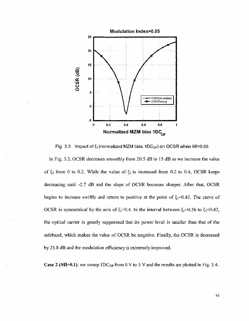
Modulation lndex=0.05
CO
01 CO o O
25
20
15
10
-5
-V /
— • — CSR(Simulation) - • — CSR(Theory)
0.2 0.4 0.6 0.8
Normalized MZM bias 1DC OP
Fig. 3.3 Impact of ^ (normalized MZM bias 1DC0P) on OCSR when Ml=0.05
In Fig. 3.3, OCSR decreases smoothly from 20.5 dB to 15 dB as we increase the value
of ^j from 0 to 0.2. While the value of ^ is increased from 0.2 to 0.4, OCSR keeps
decreasing until -2.7 dB and the slope of OCSR becomes sharper. After that, OCSR
begins to increase swiftly and return to positive at the point of ^i=0.42. The curve of
OCSR is symmetrical by the axis of ^i=0.4. In the interval between ^i=0.36 to ^i=0.42,
the optical carrier is greatly suppressed that its power level is smaller than that of the
sideband, which makes the value of OCSR be negative. Finally, the OCSR is decreased
by 25.8 dB and the modulation efficiency is extremely improved.
Case 2 (MI=0.1): we sweep IDCQP from 0 V to 5 V and the results are plotted in Fig. 3.4.
45
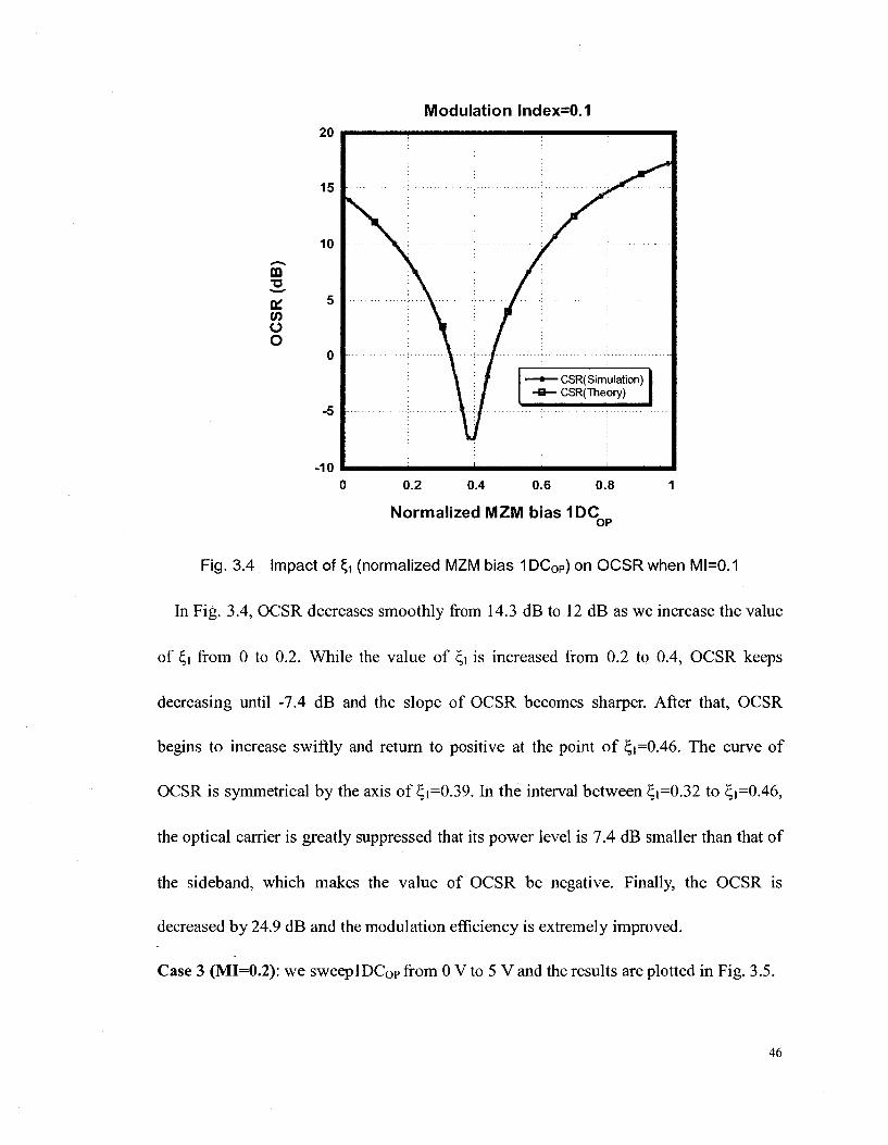
Modulation lndex=0.1
CQ
o o
20
15
10
-10 0.2 0.4 0.6 0.8
Normalized MZM bias 1DC OP
Fig. 3.4 Impact of ^ (normalized MZM bias 1DC0p) on OCSR when Ml=0.1
In Fig. 3.4, OCSR decreases smoothly from 14.3 dB to 12 dB as we increase the value
of £j from 0 to 0.2. While the value of £i is increased from 0.2 to 0.4, OCSR keeps
decreasing until -7.4 dB and the slope of OCSR becomes sharper. After that, OCSR
begins to increase swiftly and return to positive at the point of ^i=0.46. The curve of
OCSR is symmetrical by the axis of £i=0.39. In the interval between ^i=0.32 to £i=0.46,
the optical carrier is greatly suppressed that its power level is 7.4 dB smaller than that of
the sideband, which makes the value of OCSR be negative. Finally, the OCSR is
decreased by 24.9 dB and the modulation efficiency is extremely improved.
Case 3 (MI=0.2): we sweeplDC0p from 0 V to 5 V and the results are plotted in Fig. 3.5.
46

CO TO,
DC V) O O
15
-15
Modulation lndex=0.2
0.2 0.4 0.6 0.8
Normalized MZM bias 1DC OP
Fig. 3.5 Impact of ^ (normalized MZM bias 1DC0P) on OCSR when Ml=0.2
In Fig. 3.5, OCSR decreases smoothly from 8.0 dB to 5.5 dB as we increase the value
of £i from 0 to 0.1. While the value of E,y is increased from 0.2 to 0.37, OCSR keeps
decreasing until -11 dB and the slope of OCSR becomes sharper. After that, OCSR begins
to increase swiftly and return to positive at the point of £1=0.5. The curve of OCSR is
symmetrical by the axis of ^=0.37. In the interval between £i=0.22 to £i=0.5, the optical
carrier is greatly suppressed that its power level is 11 dB smaller than that of the sideband,
which makes the value of OCSR be negative. Finally, the OCSR is decreased by 22.7 dB
and the modulation efficiency is extremely improved.
Case 4 (MI=0.5): we sweepIDCQP from 0 V to 5 V and the results are plotted in Fig. 3.6.
47
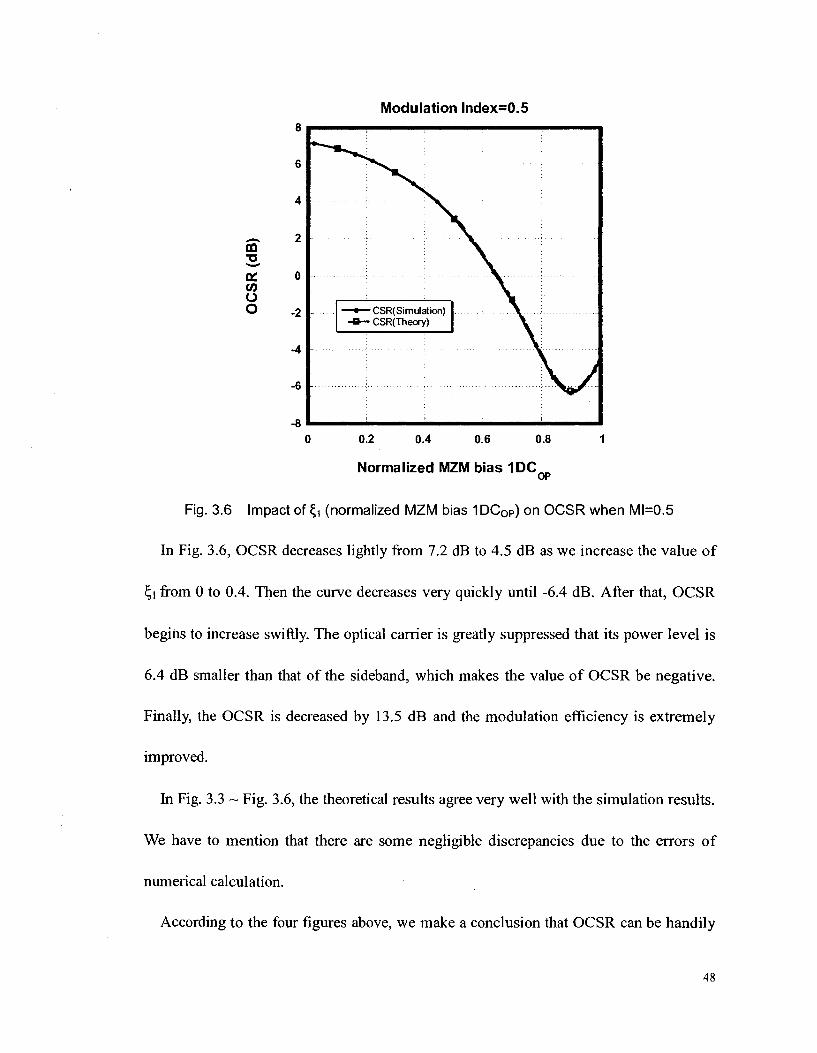
Modulation lndex=0.5
6
4
—. 2
03
o7 o CO o O .2
-4
- -
~Z: CSR(Simulation) CSR(Theory)
t
. . ^ ^ / . .
0.2 0.4 0.6 0.8
Normalized MZM bias 1DC OP
Fig. 3.6 Impact of ^ (normalized MZM bias 1DCOP) on OCSR when Ml=0.5
In Fig. 3.6, OCSR decreases lightly from 7.2 dB to 4.5 dB as we increase the value of
^i from 0 to 0.4. Then the curve decreases very quickly until -6.4 dB. After that, OCSR
begins to increase swiftly. The optical carrier is greatly suppressed that its power level is
6.4 dB smaller than that of the sideband, which makes the value of OCSR be negative.
Finally, the OCSR is decreased by 13.5 dB and the modulation efficiency is extremely
improved.
In Fig. 3.3 ~ Fig. 3.6, the theoretical results agree very well with the simulation results.
We have to mention that there are some negligible discrepancies due to the errors of
numerical calculation.
According to the four figures above, we make a conclusion that OCSR can be handily
48

adjusted within a large range by setting IDCOP and 2DCOP properly. The upper boundary
of the range may reach over 20 dB and the lower boundary may arrive at -11 dB. When
both IDCop and 2DCopare set to 0, the effect of our modulation technique is equal to that
of typical OSSB. Therefore, we can observe the modulation efficiency of typical OSSB at
the point of ^i=0 from Fig. 3.3 ~ Fig. 3.5. For detail, the values of OCSR corresponding
to MI=0.05, 0.1, 0.2 are 20.4 dB, 14.3 dB, 8 dB respectively. In Section 1.3, we
mentioned that 0 dB is the optimum value for OCSR to maximize the performance of one
RF sub-carrier system. We define the effective improvement of OCSR as the difference
between the initial OCSR (the OCSR corresponding to typical OSSB) and the optimum
OCSR, thus the improvements under our definition are 20.4 dB, 14.3 dB and 8 dB
corresponding to MI-0.05, 0.1 and 0.2. It can be concluded that our modulation
technique is more effective and efficient to improve OCSR in small MI cases than in
large MI cases.
Referring to Fig. 2.1, the phases of the optical carriers along Pathl and Path3 are
shifted by a constant when IDCOP and 2DCOP bias are fixed, even though the values of
Mis are different. As introduced in Chapter 1, our modulation technique uses phase
shifted optical carriers along Pathl and Path3, E1+E3, to interfere with RF modulated
optical carriers along Path2 and Path4, E2+E4. In case of E1+E3 and E2+E4 have identical
phase, the constructive interference will happen; otherwise, the destructive interference
between two terms will happen. If E1+E3 have a 7t-phase difference from E2+E4, the final
optical carrier will be suppressed most i.e. the most negative values of OCSR in Fig. 3.3
49

~ Fig. 3.6. The phase shift of optical carrier E|+E3 depends merely on IDCOP and 2DCOP,
thus the improvements of OCSR when MI=0.05, 0.1 and 0.2 should almost be the same
due to the identical value of 2DCop and sweeping range of IDCOP- After OCSR decreases
to the minimum, it starts to increase along the symmetrical track as the decreasing track.
We can claim that all the curves are symmetrical by an approximately identical axis
(^i=0.4, ^i=0.39 and 4i=0.37). These are due to the same phase shift range caused by the
identical 2DCOP and the same sweeping range of IDCop. The slight differences of both
OCSR improvement range and axis are caused by difference initial phase of the RF
modulated optical carriers along Path2 and Path4. Moreover, we can also predict that all
the curves are periodic, because of the characteristic of DE-MZM. In our DE-MZM, the
voltage inducing 7i-phase shift is 5 V, which means the phase of optical carrier experience
% shift when optical carrier goes through the path driven by 5 V. So when 10 V is
employed, no change will happen to its phase.
3.1.3 Impact of OCSR on RF output power and SNR
According to [21], OCSR places enormous influence on the transmission performance
in the fiber-radio links. Smaller OCSR indicates higher modulation efficiency and 0 dB is
the optimum value for OCSR. In this section, we use two parameters, RF output power
and SNR, to measure and quantify the improvement caused by our modulation technique.
As mentioned in Section 1.2.4, only HDs exist when one RF signal is applied to modulate
optical carrier. In Fig. 2.4, we can find HD terms are so far away from fundamental RF
50

sideband that it can be easily filtered out by electrical filters after PD. Therefore, in this
case, only shot noise and thermal noise are considered as the noise sources. Our
theoretical analysis verifies that OCSR has little influence on these noise sources.
Case 1 (MI=0.05): we measure the RF output power and SNR with different OCSR and
the results are shown in Fig. 3.7 and Fig. 3.8.
Modulation lndex=0.05 -40
-45
? CO
o Q.
O. -55
* -60
-65 -5 0 5 10 15 20 25
OCSR (dB)
Fig. 3.7 Impact of OCSR on RF output power when Ml=0.05
51

Modulation lndex=0.05 60 I " I — — " T " ' I !
55
T3,
z W 45
40
35 -5 0 5 10 15 20 25
OCSR (dB)
Fig. 3.8 Impact of OCSR on SNR when Ml=0.05
As can be seen in Fig. 3.7 and Fig. 3.8, the curves have the relatively same shape,
which proves that the noise power changes negligibly and can be considered as a constant.
Both RF output power and SNR increase evidently when OCSR decreases from the initial
point of OCSR=23.2dB. When OCSR measures up to 0 dB, both the RF output power
and SNR reach the peak value. After that, they start to decrease. It is well-shown in both
figures that the optimum value of OCSR is 0 dB so as to maximize the RF output power
and SNR. The total improvements of them are 17.1 dB and 16.9 dB respectively.
Case 2 (MI=0.1): we measure the RF output powers and SNR under different OCSR and
the results are plotted in Fig. 3.9 and Fig. 3.10.
52

Modulation lndex=0.1
£
CO
1 o Q. 3
a 3
o
-42
-44
-46
-48
-50
u. -52
DC
-54
-56
••»• RF(SimuIation) - B - RF(Theory)
-10 -5 0 5 10 15 20
OCSR (dB)
Fig. 3.9 Impact of OCSR on RF output power when Ml=0.1
Modulation lndex=0.1
CD ;o, tc z to
58
56
54
52
50
48
46
44
....
jr
1
2ij^;
- »" SNR(Simulation) - « — SNR(Theory)
-10 -5 0 5 10 15 20
OCSR (dB)
Fig. 3.10 Impact of OCSR on SNR when Ml=0.1
53

As can be seen in Fig. 3.9 and Fig. 3.10, the curves have the same shape, which proves
that the noise power changes negligibly and can be considered as a constant. Both RF
output power and SNR increase evidently when OCSR decreases from the initial point of
OCSR=17.3 dB. When OCSR measures up to 0 dB, both the RF output power and SNR
reach the peak value. After that, they start to decrease. It is well-shown in both figures
that the optimum value of OCSR is 0 dB so as to maximize the RF output power and
SNR. The total improvements of them are 11.1 dB and 10.9 dB respectively.
Case 3 (MI=0.2): we measure the RF output powers and SNR under different OCSR and
the results are plotted in Fig. 3.11 and Fig. 3.12.
Modulation lndex=0.2
E CQ
I O
3 Q.
+ • •
3 o UL
on
-43
-44
-45
-46
-47
-48
-49
-50 -15 -10
HB— RF(Theory)
^ ^ ^ ^ ^ ^ ^ j
-5 0 5
OCSR (dB)
10 15
Fig. 3.11 Impact of OCSR on RF output power when MN0.2
54

Modulation lndex=0.2
CD
on z
57
56
55
54
53
52
51
50
mfmmm^ —*— SNR(Simulation)
-S— SNR(Theory)
-15 -10 -5 0 5 10 15
OCSR (dB)
Fig. 3.12 Impact of OCSR on SNR when Ml=0.2
As can be seen in Fig. 3.11 and Fig. 3.12, the curves have the relatively same shape,
which proves that the noise power changes negligibly and can be considered as a constant.
Both RF output power and SNR increase evidently when OCSR decreases from the initial
point of OCSR=11.7 dB. When OCSR measures up to 0 dB, both RF output power and
SNR reach the peak value. After that, they start to decrease. It is well-shown in both
figures that the optimum value of OCSR is 0 dB so as to maximize the RF output power
and SNR. The total improvements of them are 5.2 dB and 5.0 dB respectively.
Case 4 (MI=0.5): we measure the RF output powers and SNR under different OCSR and
the results are plotted in Fig. 3.13 and Fig. 3.14.
55

Modulation lndex=0.5 -42.5
-43
-43.5
-44
-44.5
-45
-45.5
- B -RF(Simulation) RF(Theory)
i t i ;
- 6 - 4 - 2 0 2 4 6 8
OCSR (dB)
.13 Impact of OCSR on RF output power when Ml=0.5
Modulation lndex=0.5 57.5
57
56.5
56
55.5
55
54.5
—•*— SNR( Simulation) -B— SNR(Theory)
- 6 - 4 - 2 0 2 4 6 8
OCSR (dB)
Fig. 3.14 Impact of OCSR on SNR when Ml=0.5

As can be seen in Fig. 3.13 and Fig. 3.14, the curves have the relatively same shape,
which proves that the noise power changes negligibly and can be considered as a constant.
Both RF output power and SNR increase evidently when OCSR decreases from the initial
point of OCSR=7 dB. When OCSR measures up to 0 dB, both RF output power and SNR
reach the peak value. After that, they start to decrease. It is well-shown in both figures
that the optimum value of OCSR is 0 dB so as to maximize the RF output power and
SNR. The total improvements of them are 2.3 dB and 2.1 dB respectively.
All the curves from numerical analysis agree very well with those from analytical
analysis, except of very little discrepancy due to the numerical calculation errors, the rest
portions of results exactly match up with each other.
The figures above in this section indicate that when the absolute value of OCSR
decreases, both RF output power and SNR increase, which achieve the maximum values
at OCSR=0 dB. In the case of MI=0.05, the optimum OCSR happens at the point of
^i=0.42, £2=1.06, while the RF output power and SNR achieve the improvements of 17.1
dB and 16.9 dB respectively. In the case of MI=0.1, the optimum OCSR happens at the
point of £]=0.46, ^2=l-06 while the RF output power and SNR achieve the improvements
of 11.1 dB and 10.9dB respectively. In the case of MI=0.2, the optimum OCSR happens
at the point of ^i=0.52, ^>=l-06 while RF output power and SNR gain 5.2 dB and 5.0 dB
improvement respectively. In MI=0.5 case, the optimum OCSR happens at the point of
^i=0.64, ^2=0 while the RF output power and SNR achieve the improvements of 2.3 dB
and 2.1 dB respectively. Based on those four cases, we make a conclusion that our
57

proposed modulation technique is much more effective in small MI cases than in large
MI cases.
Why the improvement in small-MI cases is much greater than those in large-MI cases
can be explained from two aspects. First, the effective adjustable range of OCSR is
different. In small-MI cases, OCSR can be improved a lot because optical signal is very
weakly modulated. If the effective OCSR range is large, we can make great improvement
of RF output power and SNR. Second, HDs are different. Small MI leads to negligible
HDs compared with fundamental RF component and optical carrier. When the modulated
optical signal with suppressed optical carrier is amplified by EDFA, the fundamental RF
component and optical carrier gain almost all the pump power from EDFA and nearly no
power is consumed by HD terms. However, as MI increases, the HDs become larger and
consume certain portion of pump power while amplified by EDFA, which wastes lots of
energy and makes the modulation technique less efficient.
The situation that an optimum OCSR exists is due to interplay the optical power
between optical carrier and sideband and the RF output power and SNR mainly depends
on the square root of the product of optical carrier and sideband. When the output power
of EDFA is fixed at -5dBm, the sum of optical carrier and sideband is almost a constant,
and their product increases when the power value of optical carrier and sideband get close
to each other. When their power value is identical, 0 dB OCSR is obtained, and their
product reaches the peak point. RF output power and SNR are maximized by optimizing
OCSR.
58

3.1.4 Phase sensitivity of proposed modulation technique
Our proposed modulation technique consists of two DE-MZMs which locates upper
and lower branch respectively. In both theoretical analysis and simulation, we assume
that Branch 1 and Branch2 have identical initial phase. However, it is not applicable in
practical uses. The different initial phase along the two branches may cause phase
imbalance of the two parallel DE-MZMs. Thus it is highly necessary to investigate
whether modulation efficiency is sensitive to the phase imbalance of the two parallel
DE-MZMs. In the simulation, we insert a phase modulator after DE-MZM1. The phase
modulator is driven by a DC source and the value is set to 0.06 V. The initial phases of the
phase modulator are chosen at 0° , 15° , 30° respectively. Fig. 3.15 ~ Fig. 3.18 show
the situations when MI=0.05, 0.1, 0.2 and 0.5 respectively.
Modulation lndex=0.05
oi CO O O
0.2 0.4 0.6 0.8 1
Normalized MZM bias 1DC_ OP
Fig. 3.15 Phase sensitivity when Ml=0.05
59

Modulation lndex=0.1 15
10
-10 0.1 0.2 0.3
Normalized MZM bias 1DC
-42
-44 J, •n
O c
-46 "O r »
-o O
-48 I "a. CO
-50 1
-52
OP
Fig. 3.16 Phase sensitivity when Ml=0.1
Modulation lndex=0.2
Normalized MZM bias 1DC OP
Fig. 3.17 Phase sensitivity when Ml=0.2
60

Modulation lndex=0.5 10
5
ST •a ttf ° (0 o o
-5
-10 0 0.2 0.4 0.6 0.8 0.9
Normalized MZM bias 1DC OP
Fig. 3.18 Phase sensitivity when Ml=0.1
All the figures display that the curves with different initial phase change very little and
modulation efficiency using our proposed technique is not sensitive to the phase
imbalance of the two parallel DE-MZMs.
3.2 Proposed modulator driven by two RF signals
In the previous section, we investigated how to optimize OCSR by adjusting DCop and
how OCSR impacts the performance of system when only one RF signal is applied.
However, the optimum OCSR has not been studied when two RF signals are applied. In
the following, we investigate whether our modulation technique is effective to improve
the performance of two RF signals system and whether the optimum OCSR to maximize
the performance is still 0 dB.
.. - - :-,.---'''
—•"" - CSR(0°)
-•—CSR(15°)
""+—CSR(30°)
i
^ " " " I V - -
V/f -* • I k
: / ^ \ : * Ik.
. - / i \-H / \ ^ \
* \ »
• * - RF(0°)
" » " R F ( 1 5 ° )
RF(30°)
-- -'• -
-•*£.
-43
-44
-45
7) -n O c
"O C r*
TJ o $ (0
-46 ~ DO
-47 ""
.AH
61

As the theoretical analysis in Section 2.2.2, DCOP influences OCSR the same way
regardless one RF signal or two RF signals, which will be verified in the following
section. Section 3.2.2 will describe how OCSR influences RF output power and IM3. In
Section 3.2.3, we will investigate whether the frequency of RF signal will influence the
system performance. In simulations of Sections 3.2.1 and 3.2.2, two RF signals at the
frequencies of 5 GHz and 6 GHz are applied to our modulator.
3.2.1 Impact of lDCOPand 2DCOP on OCSR
The meaning of optimizing OCSR was introduced in Section 3.1.2. For the adjustment
of OCSR, the effect of sweeping IDCOP while keeping 2DCOP fixed is equivalent to that
of sweeping 2DCop while keeping IDCOP fixed. In the thesis, we sweep IDCOP and fix
the normalized value of 2DCOP, £,2, at 1.06 for both extra small and small Mis, while bji is
placed to 0 for medium MI. In the following figures, the results of theoretical analysis are
also illustrated and compared with the simulation results.
Case 1 (MI=0.05): we sweep IDCOP from 0 V to 5V and the result is plotted in Fig. 3.19.
62

Modulation lndex=0.05
m
a:
o O
25
20
15
10
-5
V J
—•— CSR(Simulalion) • *— CSR(Theory)
0.2 0.4 0.6 0.8
Normalized MZM bias 1DC OP
Fig. 3.19 Impact of 1DC0p on OCSR when Ml=0.05
In Fig. 3.19, OCSR decreases smoothly from 20.5 dB to 15 dB as we increase the
value of 4i from 0 to 0.2. While the value of 4i is increased from 0.2 to 0.4, OCSR keeps
decreasing until -2.7 dB and the slope of OCSR becomes sharper. After that, OCSR
begins to increase swiftly and return to positive at the point of ^i=0.42. The curve of
OCSR is symmetrical by the axis of £, =0.4. In the interval between ^i=0.36 to £i=0.42,
the optical carrier is greatly suppressed that its power level is smaller than that of the
sideband, which makes the value of OCSR be negative. Finally, the OCSR is decreased
by 25.8 dB and the modulation efficiency is extremely improved.
Case 2 (MI=0.1): we sweep IDCOP from 0 V to 5V and the result is plotted in Fig. 3.20.
63

Modulation lndex=0.1 20
15
10
CQ
w o o
-10
—•— CSR( Simulation) -a— CSR( Theory)
0.2 0.4 0.6 0.8
Normalized MZM bias 1DC OP
Fig. 3.20 Impact of 1DC0P on OCSR when Ml=0.1
In Fig. 3.20, OCSR decreases smoothly from 14.3 dB to 12 dB as we increase the
value of ^i from 0 to 0.2. While the value of ^i is increased from 0.2 to 0.4, OCSR keeps
decreasing until -7.4 dB and the slope of OCSR becomes sharper. After that, OCSR
begins to increase swiftly and return to positive at the point of ^i=0.46. The curve of
OCSR is symmetrical by the axis of £, =0.39. In the interval between £,i=0.32 to £i=0.46,
the optical carrier is greatly suppressed that its power level is 7.4 dB smaller than that of
the sideband, which makes the value of OCSR be negative. Finally, the OCSR is
decreased by 24.9 dB and the modulation efficiency is extremely improved.
Case 3 (MI=0.2): we sweep IDCQP from 0 V to 5V and the result is plotted in Fig. 3.21.
64

CO
a: to o o
15
10
-5
-10
-15
Modulation lndex=0.2
- •— CSR( Simulation) •a— CSR(Theory)
0.2 0.4 0.6 0.8
Normalized MZM bias 1DC OP
Fig. 3.21 Impact of 1DC0P on OCSR when Ml=0.2
In Fig. 3.21, OCSR decreases smoothly from 8.0 dB to 5.5 dB as we increase the value
of £i from 0 to 0.1. While the value of E,\ is increased from 0.2 to 0.37, OCSR keeps
decreasing until -11 dB and the slope of OCSR becomes sharper. After that, OCSR begins
to increase swiftly and return to positive at the point of ^i=0.5. The curve of OCSR is
symmetrical by the axis of £, =0.37. In the interval between ^i=0.22 to ^=0.5, the optical
carrier is greatly suppressed that its power level is 11 dB smaller than that of the sideband,
which makes the value of OCSR be negative. Finally, the OCSR is decreased by 22.7 dB
and the modulation efficiency is extremely improved.
Case 4 (MI=0.5): we sweep IDCQP from 0 V to 5V and the result is plotted in Fig. 3.22.
65

Modulation lndex=0.5
CD
(/> O O —•— CSR( Simulation)
-B— CSR(Theory)
1 1 ! 1
0.2 0.4 0.6 0.8
Normalized MZM bias 1DC, OP
Fig. 3.22 Impact of 1DCOP on OCSR when Ml=0.5
In Fig. 3.22, OCSR decreases lightly from 7.2 dB to 4.5 dB as we increase the value of
£i from 0 to 0.4. Then the curve decreases very quickly until -6.4 dB. After that, OCSR
begins to increase swiftly. The optical carrier is greatly suppressed that its power level is
6.4 dB smaller than that of the sideband, which makes the value of OCSR be negative.
Finally, the OCSR is decreased by 13.5 dB and the modulation efficiency is extremely
improved.
Comparing Section 3.1.2 with Section 3.2.1, it is exceptionally apparent that 4, £i, and
£,2 affect OCSR here the same way as in the case of one RF signal,
3.2.2 Impact of OCSR on RF output power and IM3
In this section, we investigate how OCSR impacts the performance of the system. We
66
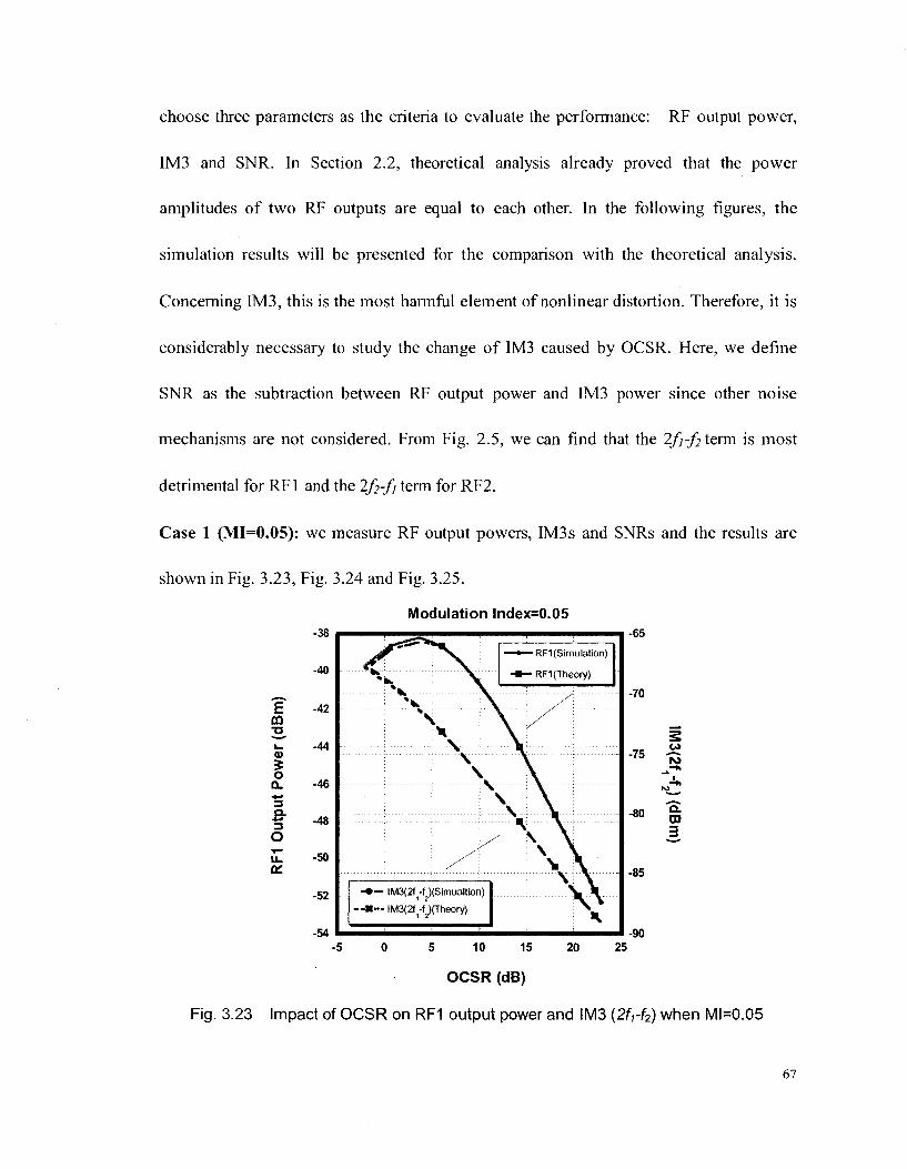
choose three parameters as the criteria to evaluate the performance: RF output power,
IM3 and SNR. In Section 2.2, theoretical analysis already proved that the power
amplitudes of two RF outputs are equal to each other. In the following figures, the
simulation results will be presented for the comparison with the theoretical analysis.
Concerning IM3, this is the most harmful element of nonlinear distortion. Therefore, it is
considerably necessary to study the change of IM3 caused by OCSR. Here, we define
SNR as the subtraction between RF output power and IM3 power since other noise
mechanisms are not considered. From Fig. 2.5, we can find that the 2/}-/? term is most
detrimental for RF1 and the 2/?-/; term for RF2.
Case 1 (MI=0.05): we measure RF output powers, IM3s and SNRs and the results are
shown in Fig. 3.23, Fig. 3.24 and Fig. 3.25.
Modulation lndex=0.05
£ CO
Q)
o Q. * - » 3 Q.
+•• 3
o
Q. 00 3
OCSR (dB)
Fig. 3.23 Impact of OCSR on RF1 output power and IM3 (2frf2) when Ml=0.05
67

Modulation lndex=0.05
E
0)
o Q.
"5 Q. 3
o CM UL
-38
-40
-42
-44
-46
-48
-50
-52
-54
-RF2(Simulation)
RF2(Theory)
-65
-70
-75
-80
-85
CO
ro
Q.
3
-90 -5 5 10 15 20 25
OCSR (dB)
Fig. 3.24 Impact of OCSR on RF2 output power and IM3 (2f2-f1) when Ml=0.05
Modulation lndex=0.05
CO
z to
38
36
34
32
30
28
fl
V
— • — SNR(Simulation) HB— SNR(Theory)
.._
-5 0 5 10 15 20 25
OCSR (dB)
Fig. 3.25 Impact of OCSR on SNR when Ml=0.05
68

In the above three figures, the curves from simulation results match very well with
those from theoretical analysis and also RF1 output power in Fig. 3.23 is identical to RF2
output power in Fig. 3.24. As OCSR gets to decrease, the RF output powers keep
increasing until OCSR=3 dB and start to decrease after that; The IM3 powers also keep
increasing very quickly. Thus we can make a conclusion that RF output powers are
maximized at OCSR=3 dB and IM3 arrives at the peak point at the most negative OCSR.
From OCSR=21 dB to OCSR=3 dB, 14.5 dB improvements of RF output powers are
achieved. In Fig. 3.25, as OCSR decreases from 21 dB, SNR decreases very slowly in the
beginning but highly fast after, which is due to that at first IM3 increases slightly faster
than RF output powers but much faster later.
Case 2 (MI=0.1): we measure RF output powers, IM3s and SNRs and the results are
shown in plot Fig. 3.26, Fig. 3.27 and Fig. 3.28.
69

Modulation lndex=0.1 -37
-RF1 (Simulation)
• RFI(Theory)
-55
5
ro
Q. CO 3
Impact of OCSR on RF1 output power and IM3 (2f1-f2) when Ml=0.1
Modulation lndex=0.1 -37
-38
-39
-40
-41
-42
-43
-44
RF2(Simulation)
RF2(Theory)
-10
-55
-60
-65 J1
a. US 3
-70
-75 0 5 10
OCSR (dB)
15
Impact of OCSR on RF2 output power and IM3 (2f2-fi) when MN0.1
70

Modulation lndex=0.1
DQ
on
to
32
30
28
26
24
22
20
18
16 -10 0 5
OCSR (dB)
1 !
t SNR(Simulation) - •— SNR(Theory)
10 15
Fig. 3.28 Impact of OCSR on SNR when Ml=0.1
In the above three figures, the curves from simulation results match very well with
those from theoretical analysis and also RF1 output power in Fig. 3.26 is identical to RF2
output power in Fig. 3.27. As OCSR gets to decrease, the RF output powers keep
increasing until OCSR=3 dB and start to decrease after that; the IM3 powers also keep
increasing very quickly. Thus we can make a conclusion that RF output powers are
maximized at OCSR=3 dB and IM3 arrives at the peak point at the most negative OCSR.
From OCSR=14.4 dB to OCSR=3 dB, 6.4 dB improvements of RF output powers are
achieved. In Fig. 3.28, as OCSR decreases from 14.4 dB, SNR decreases very slowly in
the beginning but highly fast after, which is due to that at first IM3 increases slightly
faster than RF output powers but much faster later.
71
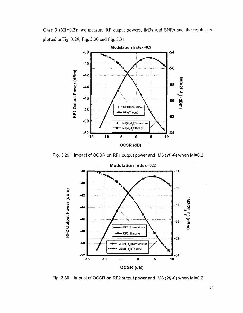
Case 3 (MI=0.2): we measure RF output powers, IM3s and SNRs and the results are
plotted in Fig. 3.29, Fig. 3.30 and Fig. 3.31.
Modulation lndex=0.2
£ m T3
<0
o a. •»-*
3 Q .
3
o a:
-38
-40
-42
-44
•46
-48
-50
-52
- • - 11 /̂13(2 -̂̂ ((Simulation)
— * - - IM3(2fi-f2)(Theory)
-54
-56
•58
60
• i t .
"a DO
-62
-15 -10 10 -64
-5 0 5
OCSR (dB)
Fig. 3.29 Impact of OCSR on RF1 output power and IM3 (2frf2) when Ml=0.2
Modulation lndex=0.2
E CO 2, i -a> 5 o a. + J 3 Q.
-4-1
3
o CM U .
(£.
-38
-40
-42
-44
-46
-48
-50
-52
-54
-15 -10 -5 0 5
OCSR (dB)
Fig. 3.30 Impact of OCSR on RF2 output power and IM3 {2f2-fi) when Ml=0.2
72

Modulation lndex=0.2
DC Z
25
20
15
10
-5
-10
—«•— SNR( Simulation) -ft— SNR(Theory)
-20 -15 -10 -5 0 5 10
OCSR (dB)
Fig. 3.31 Impact of OCSR on SNR when Ml=0.2
In the above three figures, the curves from simulation results match very well with
those from theoretical analysis and also RF1 output power in Fig. 3.29 is identical to RF2
output power in Fig. 3.30. As OCSR gets to decrease, the RF output powers keep
increasing until OCSR=3 dB and start to decrease after that; the IM3 powers also keep
increasing very quickly. Thus we can make a conclusion that RF output powers are
maximized at OCSR=3 dB and IM3 arrives at the peak point at the most negative OCSR.
From OCSR=9.5 dB to OCSR=3 dB, 2.4 dB improvements of RF output powers are
achieved. In Fig. 3.31, as OCSR decreases from 9.5 dB, SNR decreases very slowly in
the beginning but highly fast after, which is due to that at first IM3 increases slightly
faster than RF output powers but much faster later.
73

Case 4 (Ml=0.5): we measure RF output powers, IM3s and SNR and the results are
shown in Fig. 3.32, Fig. 3.33 and Fig. 3.34.
Modulation lndex=0.5
01
-43.2
-43.4
E 03 TJ *. < i _
0) Z o
QL • * - »
3 Q. 3
o T—
u_
-43.6
-43.8
-44
-44.2
-44.4
-44.6
-44.8
-• ...... V
"V"
/ ' \ "NT"' \ —•—RFI(Simulation)
• *— RF1 ("Theory) ''••/ N \
/ V \ I H V
[;. i
H»— IM3(2f ̂ (Simulation)
- - * — IM3(2fi-y(Theory)
\ i
-10 0 5
OCSR (dB)
10
-42
-43
-44 &
-45
-46
DO
-47 15
Fig. 3.32 Impact of OCSR on RF1 output power and IM3 {2frf2) when Ml=0.5
74

Modulation lndex=0.5 -43.2
-43.4
-43.6
-43.8
-44
-44.2
-44.4
-44.6
-44.8
-M— I M3(2f-f XTheory)
-42
-43
" 4 4 K>
-45
-46
CD
-47
-10 0 5
OCSR (dB)
10 15
mpact of OCSR on RF2 output power and IM3 (2f2-f1) when Ml=0.5
Modulation lndex=0.5
-5
-10
-15
!
- » SNR(Sim ulation) - H — SNR(Theory)
-10 -5 0 5 10 15
OCSR (dB)
Fig. 3.34 Impact of OCSR on SNR when Ml=0.5
In the above three figures, the curves from simulation results match very well with
those from theoretical analysis and also Fig. 3.32 has the same shape with Fig. 3.33. As
OCSR gets to decrease, the RF output powers keep increasing until OCSR=3 dB and start
to decrease after that; the IM3 powers also keep increasing very quickly. Thus we can
make a conclusion that RF output powers are maximized at OCSR=3 dB and IM3 arrives
at the peak point at the most negative OCSR. From OCSR=13.2 dB to OCSR=3 dB, 1.3
dB improvements of RF output powers are achieved. In Fig. 3.31, as OCSR decreases
from 13.2 dB, SNR decreases very slowly in the beginning but highly fast after, which is
due to that at first IM3 increases slightly faster than RF output powers but much faster
later.
All the curves of RF output powers show that their values reach the peak when OCSR=
3dB, i.e. the optimum OCSR. This optimum OCSR exists is due to the interplay among
the optical power of optical carrier (Poc), RF1 fundamental component (Poi), and RF2
fundamental component (Pen)- From the discussion above, we know Poi is equal to Po2-
The sum of Poc, Poi andP02 is a constant when the output power of EDFA is fixed as C.
The electrical output power of RF1 (PEI) is proportional to the optical-power product of
the optical carrier and its fundamental component, i.e.,PE] oc ̂ P0CPQ] ~ ^j{C — 2Pm)Pm .
In the cases of extra small MI and small MI, the expression above is extremely accurate
because HDs and IMDs are negligible compared with Poc, Poi, and P02. From the
expression, we conclude that PEi achieves the maximum value only when P0c=2P0i=C/2,
i.e. OCSR=3 dB. The mechanism can leads to 14.5 dB, 6.4 dB, 2.4 dB and 1.3 dB
76

improvements of RF output powers when MI=0.05, 0.1, 0.2 and 0.5 respectively. Our
proposed modulation technique is still more efficient in small MI cases than in large MI
cases. That's because in small MI cases, the initial OCSR is large and can be improved
enormously. Furthermore, HDs and IMDs are much smaller than those in medium and
large MI cases. When nonlinear distortions increase tremendously, considerable portion
of pump energy from EDFA will be consumed by them, which decreases the efficiency of
our modulation technique greatly.
IM3 is another important parameter to evaluate the system performance. From the
figures above, IM3 keeps increasing quickly as OCSR decreases. As can be seen in Fig.
3-25, Fig. 3-28, Fig. 3-31 and Fig. 3-34, SNR decreases slowly at first as OCSR
decreases and decrease swiftly when OCSR is below 3 dB. The reason why SNR
decreases as OCSR decreases is that IM3 always increases faster than RF output powers.
When OCSR is below 3 dB, RF output powers begins to decrease but IM3 still continues
to increase, which leads to that SNR decrease faster.
Why SNR keeps decreasing is explained mathematically. Poc, PRF and PMI represent
the optical powers of optical carrier, fundamental RF sideband and IM3 component
respectively before EDFA. Once MI is fixed, the subtraction between PRF and Pmi
becomes a constant and we define that as C/. Another constant C? represents the fixed
output power of EDFA. Then we obtain
Poc = PRF + OCSR
P —P =C 1 RF J Ml, '-1
77

If we define G as the optical gain from EDFA, we can express SNR as
SNR = G(PRF - PIM3)P0C = QG(PRF + OCSR)
c c Q __ ^2 212
+ PKF+P,MI ^P^+OCSR-Q
Finally, we combine them together and get
SNR = cic2(PKF+ocsR) = qc2
3PRF + OCSR - C, , 2PKF-Cl
PRF+OCSR
It is concluded that SNR decreases when OCSR decreases.
3.2.3 Impact of frequencies of RF signals on SNR
The conclusion from the previous section states SNR decreases as OCSR decreases. In
this section, we investigate whether the frequencies of RF signals have an influence on
system performance. Two sets of simulations in which f2-fi is equal to 1 GHz and 2 GHz
respectively are shown in Fig. 3.35 and Fig. 3.36. In each set, we sweep the frequencies
of RF signal when OCSR=0 dB, 10 dB and 20 dB respectively and the results are plotted
in Fig. 3.35 and Fig. 3.36. SNRi is defined as the electrical power subtraction between
RF1 output and 2fi-f2 term while SNR2 is the electrical power subtraction between RF2
output and 2f2-fi term.
78

Modulation lndex=0.05 38
CO »
33. o f z OT 32
30
28
. - * K
. . .*• + 9"*"1 " • — -.».•- a -o
« _ _ —,£_._. __
— • — CSR=20dB(f)-f]=1GHz)
H9— CSR=10dB(f?-f)=1GH2)
- • — DCSR=0dB(f2-M1GHz)
~ « " C S R = 2 0 d B ( f ! - f i = 2 G H z )
- - + - • CSR=1CWB(M)=2GHz)
.-..- CSR=0dB(( i-f i=2GHz)
, . — ^ - ,
5 6 7 8 9
RF1 Frequency (GHz)
10
Fig. 3.35 Impact of RF1 frequency on SNR!
Modulation lndex=0.05 38
36
m •a
OH
z CO
34
32
30
28
LiirLli i^x. .rfr.rrr.dp
—•—CSR=20dB(f2-fi=1GHz)
-W— CSR^IOdBIM^IGHz)
- •— CSR=0dB(f -f =1GHz)
- - « - - CSR=20dB(f;-f |=2GHz)
. • + - - CSR=10dB(fJ-fl=2GHz)
CSR=0dB(fj-fi=2GHz)
6 7 8 9 10 11
RF2 Frequency (GHz)
Fig. 3.36 Impact of RF2 frequency on SNR2
Fig. 3.35 and Fig. 3.36 show the frequencies of RF signals have little influence on
SNR. Regardless what frequencies are employed, SNR will not be improved or degraded.
In the future work, we will change the ideal connection between EDFA and PD into
standard single mode fiber. In that case, the situation will be different and the frequencies
of RF signals will have great impact on SNR.
79

When two RF signals are applied to modulate optical carrier by our technique, RF
output powers will be greatly improved but SNR won't. However, several explanations
are made as follows:
1. If we use our proposed modulation technique and keep modulation index the same, RF
output power can be greatly improved and SNR will be degraded by a little degree. To
some extent, it plays the role like an amplifier. When signal goes through an amplifier, its
power will be increased but its SNR will also be slightly degraded. In addition, compared
to the weakly modulated OSSB SCM, although SNR is slightly degraded, our technique
can maximize the RF output power and make the RoF system more robust to other noise
interference.
2. In order to obtain identical RF output power, small MI modulation can be applied by
using our proposed modulation technique while large MI modulation should be applied
by employing typical OSSB SCM. In that case, SNR using our proposed modulation
technique is still larger that in typical OSSB SCM. For instance, the RF output power is
-53dBm when modulation index is equal to 0.05 in typical OSSB SCM. In order to obtain
higher RF output power i.e. -43dBm, we have two ways. One is still using typical OSSB
SCM and increasing modulation index to improve modulation efficiency. In that case,
0.12 should be chosen for £ and the corresponding SNR is 29.8dB. The other is choosing
our proposed modulation technique and improving modulation efficiency by adjusting
DCop. The corresponding SNR is 35.3dB. In all, a great improvement of SNR can be
achieved.
80

3. When paying attention to the range of SNR degradation, we find from the largest
OCSR to the optimum OCSR the SNR degradations are 4 dB, 5 dB, 1 dB and 3 dB
respectively, which is not large.
4. Although IM3 is highly detrimental to system performance, it is possible to suppress or
even avoid it by choosing frequencies of RF signals properly. If we enlarge the frequency
difference between RF signals, IM3 may be avoided completely. For instance, IM3 can
be handily filtered out by appropriate electrical filters when the frequencies of RF1 and
RF2 are 7 GHz and 10 GHz respectively.
81

Chapter 4 Conclusions and future work
4.1 Major contribution
In this thesis, a novel modulation technique using two parallel Mach-Zehnder
modulators for radio over fiber systems is proposed and then theoretical analysis is
presented. With such a modulator, we can obtain optical single sideband SCM and
adjustable optical carrier-to-sideband ratio. Two cases are considered: one RF signal and
two RF signals driving the proposed modulator, respectively. The theoretical analysis is
finally verified by computer simulations.
By both theoretical analysis and simulation, it is shown that our proposed modulation
technique can provide optical single sideband SCM and adjustable optical
carrier-to-sideband ratio. When one RF signal is applied to modulate an optical carrier,
modulation efficiency can be improved and be able to improve RF output power and
SNR considerably, and the optimized optical carrier-to-sideband ratio is found 0 dB.
However, the improved performance is limited by nonlinear distortion for large
modulation indexes. When two RF signals are employed to modulate an optical carrier,
RF output power increases with the decrease of optical carrier-sideband ratio, but IM3
power also increases and the increase rate is faster than RF output power. Thus, SNR
decreases as optical carrier-sideband ratio decreases. At optical carrier-to-sideband ratio
of 3 dB, RF output powers are maximized, rather than 0 dB for the case of one RF signal.
For both cases, the improvement using our proposed modulation technique is higher in
82
small modulation index cases than that in large modulation index cases.
The advantage of proposed novel modulation technique is that we do not need any
additional optical or electrical components after modulator to realize an optical carrier
suppressed OSSB. Compared with other methods of suppressing optical carrier, this
proposed modulation technique is simple, stable and easy to implement. Without bringing
any distortions or other detrimental terms, this proposed modulation technique can
improve the performance of RoF systems greatly.
4.2 Future work
In this work, some conditions are considered ideally in computer simulations. The laser
source, EDFA and PD are supposed to be noise free. The connection between EDFA and
PD is applied also ideally in all simulations except in Section 3.1.1. As we know, if we
use standard single mode optic fiber, chromatic terms should be added into analytical
model and the results will be different in computer simulation. Besides, only analogue RF
signal is considered here to transmit over the link. However, those digital data formats e.g.
DPSK, QPSK and QAM are also commonly utilized to transmit in RoF systems.
Therefore, we will focus on the situation when different type of signal is transmitted.
83

References
[1] H Ogawa, D Polifko and S Banba, "Millimeter-wave fiber optical systems for
personal radio communication," IEEE Trans, on Microwave Theory and Technique,
vol. 40, No. 12, pp.2294-2302, Dec. 1992.
[2] D. Wake, D. Johansson and D. Moodie, "Passive Pico-cell: a new concept in wireless
network infrastructure," Electron. Lett., vol.33, pp.404-406, Feb. 1997.
[3] D. Wake, "Radio over Fiber Systems for Mobile Applications" in Radio over Fiber
Technologies for Mobile Communications Networks, H, Al-Raweshidy, and S.
Komaki, ed. (Artech House, Inc, USA, 2002).
[4] D. Wake, and K. Beachman, "A Novel Switched Fiber Distributed Antenna System",
in Proceedings of European Conference on Optical Communications (ECOC '04),
Vol. 5, 2004, pp. 132-135.
[5] J. Capmany, B. Ortega, D. Pastor, and S. Sales, "Discrete-Time Optical Processing of
Microwave Signals", JLT, Vol. 23, No. 2, 703 - 723, (2005).
[6] G. Maury, A. Hilt, T. Berceli, B. Cabon, and A. Vilcot, "Microwave Frequency
Conversion Methods by Optical Interferometer and Photodiode", IEEE Trans. On
Microwave Theory and Techniques, Vol. 45, No. 8, 1481 - 1485, (1997).
[7] D. Wake, S. Dupont, J-P. Vilcot, A. J. Seeds, "32-QAM Radio Transmission Over
Multimode Fiber Beyond the Fiber Bandwidth", in Proceedings of the IEEE
International Topical Meeting on Microwave Photonics (MWP'01), 2001.
84
[8] D. Wake, S. Dupont, C. Lethien, J-P. Vilcot, and D. Decoster, "Radiofrequency
Transmission over Multimode Fiber for Distributed Antenna System Applications",
Electronic Letters, Vol. 37, No. 17, pp 1087 - 1089 (2001).
[9] C. Liu, A. Seeds, J. Chadha, P. Stavrinou, G. Parry, M. Whitehead, A. Krysa, and J.
Roberts, "Bi-Directional Transmission of Broadband 5.2 GHz Wireless Signals Over
Fiber Using a Multiple-Quantum-Well Asymmetric Fabry-Perot Modulator/Photo
detector", in Proceedings of the Optical Fiber Communications (OFC) Conference.
2003, Vol. 2, pp. 738 - 740.
[10] H. Al-Raweshidy, S. Komaki, ed., "Radio over Fiber Technology for the Next
Generation" in Radio over Fiber Technologies for Mobile Communications
Networks, (Artech House, Inc, USA, 2002).
[11] U. Gliese, T. N. Nielsen, S. Norskov, and K.E. Stubkjaer, "Multifunction Fiber-Optic
Microwave Links Based on Remote Heterodyne Detection", IEEE Trans. On
Microwave Theory and Techniques, vol. 46, No. 5, 458-468, (1998)
[12] G. J. Meslener, "Chromatic dispersion induced distortion of modulated
monochromatic light employing direct detection," IEEE J. Quantum Electron., vol.
QE-20, no. 10, pp. 1208-1216, Oct. 1984.
[13] H. Schmuck, "Comparison of optical millimeter-wave system concepts with regard
to chromatic dispersion," Electronic Letters, vol. 31, no. 21, pp. 1848-1849, Oct.
1995.
[14] U. Gliese, S. Norskov, and T. N. Nielsen, "Chromatic dispersion in fiber-optic
85

microwave and millimeter-wave links," IEEE Trans. Microwave. Theory Tech., vol.
44, no. 10, pp. 1716-1724, Oct. 1996.
[15] G. H. Smith, D. Novak, and Z. Ahmed, "Technique for optical SSB generation to
overcome dispersion penalties in fiber-radio systems," Electronic Letters, vol. 33, no.
1, pp. 74-75,Jan. 1997.
[16] J. Park, W. V. Sorin, and K. Y. Lau, "Elimination of the fiber chromatic dispersion
penalty on 1550 nm millimeter-wave optical transmission," Electronic Letters, vol.
33, no. 6, pp. 512-513, Mar. 1997.
[17] E.Vergnol, D. Tanguy, J. F. Cadiou, A. Carenco, and E. Penard, "Multicarrier and
m-QAM modulation based on integrated single side band lightwave source," in Proc.
Opt. Fiber Commun. Conf., San Diego, CA, Feb. 1999, pp. 224-226.
[18] E. Vourch, D. Le Berre, and D. Herve, "Lightwave single sideband wavelength
self-tunable filter using InP: Fe crystal for fiber-wireless systems," IEEE Photon.
Technol. Lett., vol. 14, no. 2, pp. 194-196, Feb. 2002.
[19] R. D. Esman and K. J. Willians, "Wideband efficiency improvement of fiber optic
systems by carrier subtraction," IEEE Photon. Technol. Lett., vol. 7, no. 2, pp.
218-220, Feb. 1995.
[20] M. J. LaGasse, W. Charczenko, M. C. Hamilton, and S. Thaniyavarn, "Optical
carrier filtering for high dynamic range fiber optic links," Electronic Letters, vol. 30,
no. 25, pp. 2157-2158, Dec. 1994.
[21] Christina Lim, Manik Attygalle etc., "Analysis of Optical Carrier-to-Sideband Ratio
86

for Improving Transmission Performance in Fiber-Radio Links", IEEE Transactions
on Microwave Theory and Techniques, vol.54 No.5, May 2006, pp.2181-2187.
[22] S. Tonda-Goldstein, D. Dolfi, J-P. Huignard, G. Charlet, and J. Chazelas,
"Stimulated brillouin scattering for microwave signal modulation depth increase in
optical links," Electronic Letters, vol. 36, no. 11, pp. 944-946, May 2000.
[23] H. Toda, T. Yamashita, T. Kuri, and K. Kitayama, "25-GHz channel spacing
DWDM multiplexing using an arrayed waveguide grating for 60-GHz band
radio-on-fiber systems," in Proc. Microw. Photon., Budapest, Hungary, Sep. 2003,
pp. 287-290.
[24] W. W. Hu, K. Inagaki, T. Tanaka, T. Ohira and A. Xu, "High SNR 50 GHz
radio-over-fiber uplink system by use of low biased Mach-Zehnder modulator
technique", Electronic Letters, 27th April 2006, vol. 42 No. 9.
87