on-chip over-voltage protection design against
TRANSCRIPT

2702 IEEE TRANSACTIONS ON ELECTRON DEVICES, VOL. 67, NO. 7, JULY 2020
On-Chip Over-Voltage Protection Design AgainstSurge Events on the CC Pin of USB
Type-C InterfaceChao-Yang Ke and Ming-Dou Ker , Fellow, IEEE
Abstract— As fast charging being a comprehensive appli-cation in universal serial bus (USB) type-C products,the high-power delivery may cause the USB type-C interfacein the high risk of surge events. Therefore, a switch realizedby high voltage N-type metal oxide semiconductor transistor(HVNMOS) has been added to the configuration channel(CC) pin to prevent the internal circuits from surge damage.However, hot carrier degradation (HCD) on the HVNMOS wasinduced by surge events, especially when the HVNMOS wasoperating in the ON-state. To mitigate HCD on the HVNMOSswitch during surge events, a new over-voltage protec-tion (OVP) design with selected voltage-level detection wasproposed and verified in a 0.15-µm BCD technology. Theproposed OVP circuit with a positive feedback is designedto turn off the gate of the HVNMOS switch for a longer timewhen surge zapping on the CC pin. The experimental resultsfrom silicon chip have successfully verified the proposedOVP structure in device level and circuit level, respectively.
Index Terms— Electrical overstress (EOS), hot carrierdegradation (HCD), overvoltage protection (OVP), surgeprotection, surge test, universal serial bus (USB) type-C.
I. INTRODUCTION
USB type-C interface recently has become popular anddrawn much attention due to the advantages of high
power delivery, fast charging, and high-speed data transmis-sion. According to the universal serial bus (USB) type-Cspecification [1], [2], in power delivery mode, the maximumvoltage level and driving current of the VBUS pin can increaseup to 20 V and 5 A, respectively. Such high power deliveryapplication makes the USB type-C interface system to be inthe risk of surge damage. Thus, not only USB type-C productswere done with ESD testing, but they were also requested withsurge testing.
For surge immunity testing, International ElectrotechnicalCommission’s international standard (IEC 61000-4-5) has
Manuscript received March 25, 2020; revised April 25, 2020; acceptedMay 1, 2020. Date of publication May 18, 2020; date of current versionJune 19, 2020. This work was supported in part by the Ministry ofEducation (MOE) through the SPROUT Project—Center for Neuromod-ulation Medical Electronics Systems of National Chiao Tung University,Taiwan and in part by the Ministry of Science and Technology (MOST),Taiwan, under Contract MOST 108-2622-8-009-001-TE1. The review ofthis article was arranged by Editor C. Duvvury. (Corresponding author:Ming-Dou Ker.)
The authors are with the Institute of Electronics, National Chiao TungUniversity, Hsinchu 300, Taiwan (e-mail: [email protected]).
Color versions of one or more of the figures in this article are availableonline at http://ieeexplore.ieee.org.
Digital Object Identifier 10.1109/TED.2020.2992383
Fig. 1. Calibrated 1.2/50-µs open-circuit voltage surge waveform with a28-V zapping voltage.
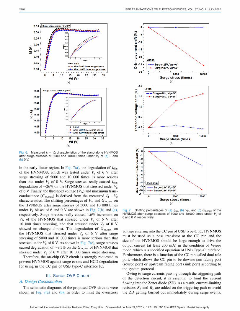
defined the method with test procedures to investigate thesurge immunity with both positive and negative surges forelectronic devices [3]. The measured surge waveform of thecalibrated open-circuit voltage with 28-V peak voltage isshown in Fig. 1, with the front time of 1.2 μs and the durationtime of 50 μs. Such a calibrated open-circuit voltage surgeis used in this work to investigate the hot carrier degrada-tion (HCD) of the high voltage N-type metal oxide semicon-ductor transistor (HVNMOS) in device level and the circuitoperation of the proposed over-voltage protection (OVP) struc-ture in circuit level.
The configuration channel (CC) pin in the USB type-Cinterface plays an important role of system protocol, includingdetecting attachment of USB ports, resolving cable orientation,and twist connections to establish USB data bus routing,discovering, and configuring VBUS, as well as configuringVCONN mode, alternate mode, and accessory mode. Therefore,if the function of the CC pin was wrong, the battery charg-ing or power supply for electronic devices could not workcorrectly, which may cause the whole electronic system ina dangerous situation. As a result, the reliability of the CCpin is really critical. Although the discrete transient voltagesuppressor (TVS) device adding to the CC pin on the printedcircuit board (PCB) had been a solution, on-chip OVP designis still strongly desired by industry for safety consideration.In recent years, some methods have been proposed againstelectrical overstress (EOS) or surge events for USB type-Cinterfaces [4]–[9].
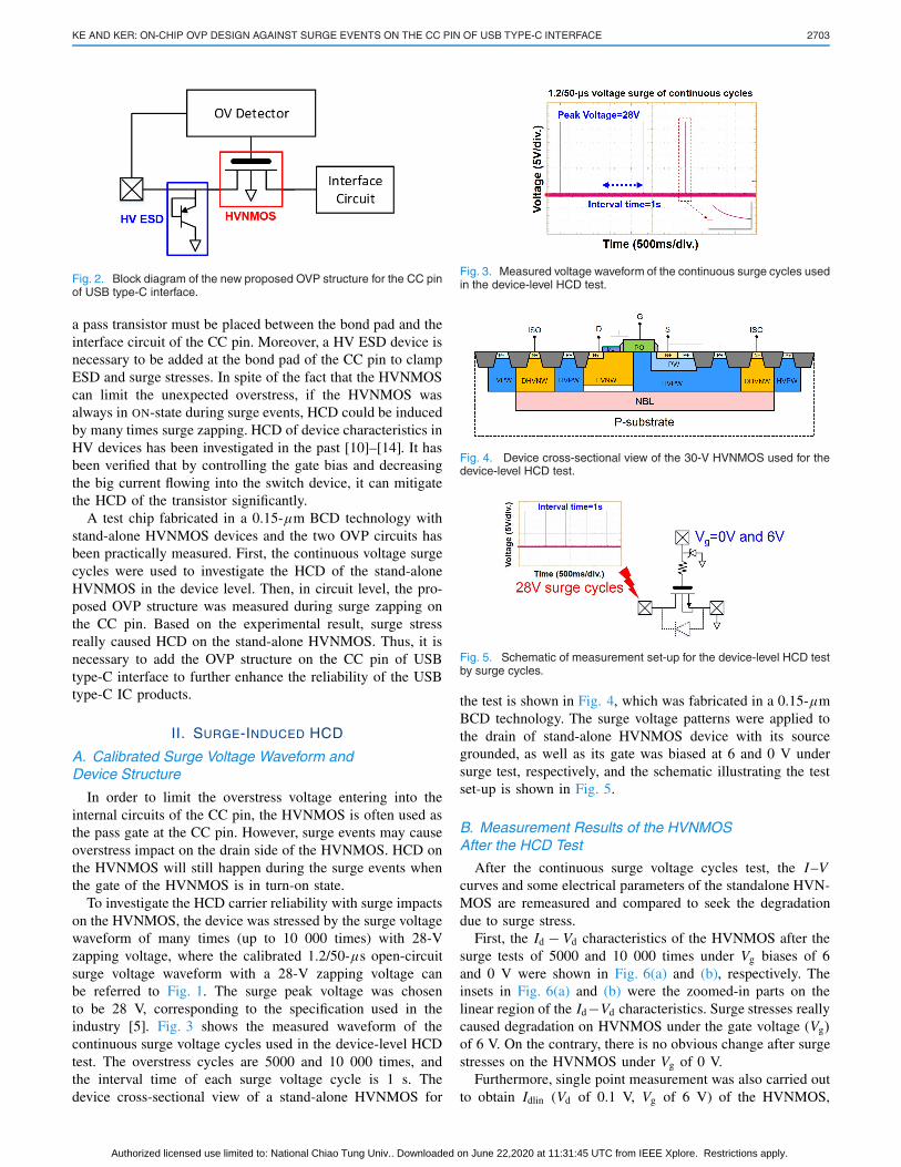
In this article, a novel OVP structure with the concept ofvoltage-level detection was proposed as shown in the blockdiagram (Fig. 2). In order to limit the overstress voltageentering into the CC pin of USB type-C IC, HVNMOS used as
0018-9383 © 2020 IEEE. Personal use is permitted, but republication/redistribution requires IEEE permission.See https://www.ieee.org/publications/rights/index.html for more information.
Authorized licensed use limited to: National Chiao Tung Univ.. Downloaded on June 22,2020 at 11:31:45 UTC from IEEE Xplore. Restrictions apply.
KE AND KER: ON-CHIP OVP DESIGN AGAINST SURGE EVENTS ON THE CC PIN OF USB TYPE-C INTERFACE 2703
Fig. 2. Block diagram of the new proposed OVP structure for the CC pinof USB type-C interface.
a pass transistor must be placed between the bond pad and theinterface circuit of the CC pin. Moreover, a HV ESD device isnecessary to be added at the bond pad of the CC pin to clampESD and surge stresses. In spite of the fact that the HVNMOScan limit the unexpected overstress, if the HVNMOS wasalways in ON-state during surge events, HCD could be inducedby many times surge zapping. HCD of device characteristics inHV devices has been investigated in the past [10]–[14]. It hasbeen verified that by controlling the gate bias and decreasingthe big current flowing into the switch device, it can mitigatethe HCD of the transistor significantly.
A test chip fabricated in a 0.15-μm BCD technology withstand-alone HVNMOS devices and the two OVP circuits hasbeen practically measured. First, the continuous voltage surgecycles were used to investigate the HCD of the stand-aloneHVNMOS in the device level. Then, in circuit level, the pro-posed OVP structure was measured during surge zapping onthe CC pin. Based on the experimental result, surge stressreally caused HCD on the stand-alone HVNMOS. Thus, it isnecessary to add the OVP structure on the CC pin of USBtype-C interface to further enhance the reliability of the USBtype-C IC products.
II. SURGE-INDUCED HCD
A. Calibrated Surge Voltage Waveform andDevice Structure
In order to limit the overstress voltage entering into theinternal circuits of the CC pin, the HVNMOS is often used asthe pass gate at the CC pin. However, surge events may causeoverstress impact on the drain side of the HVNMOS. HCD onthe HVNMOS will still happen during the surge events whenthe gate of the HVNMOS is in turn-on state.
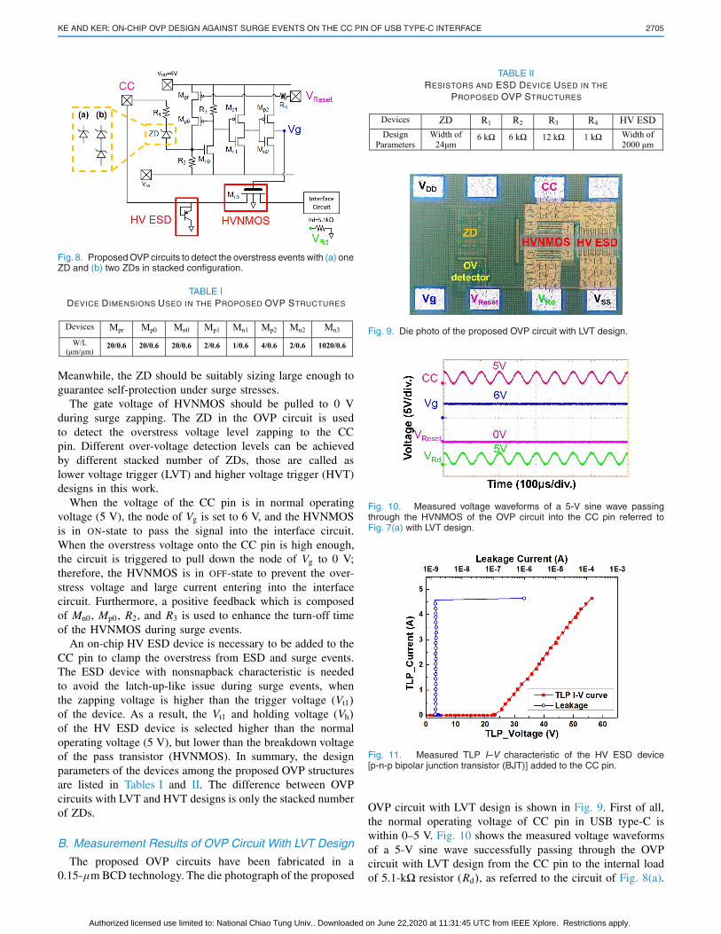
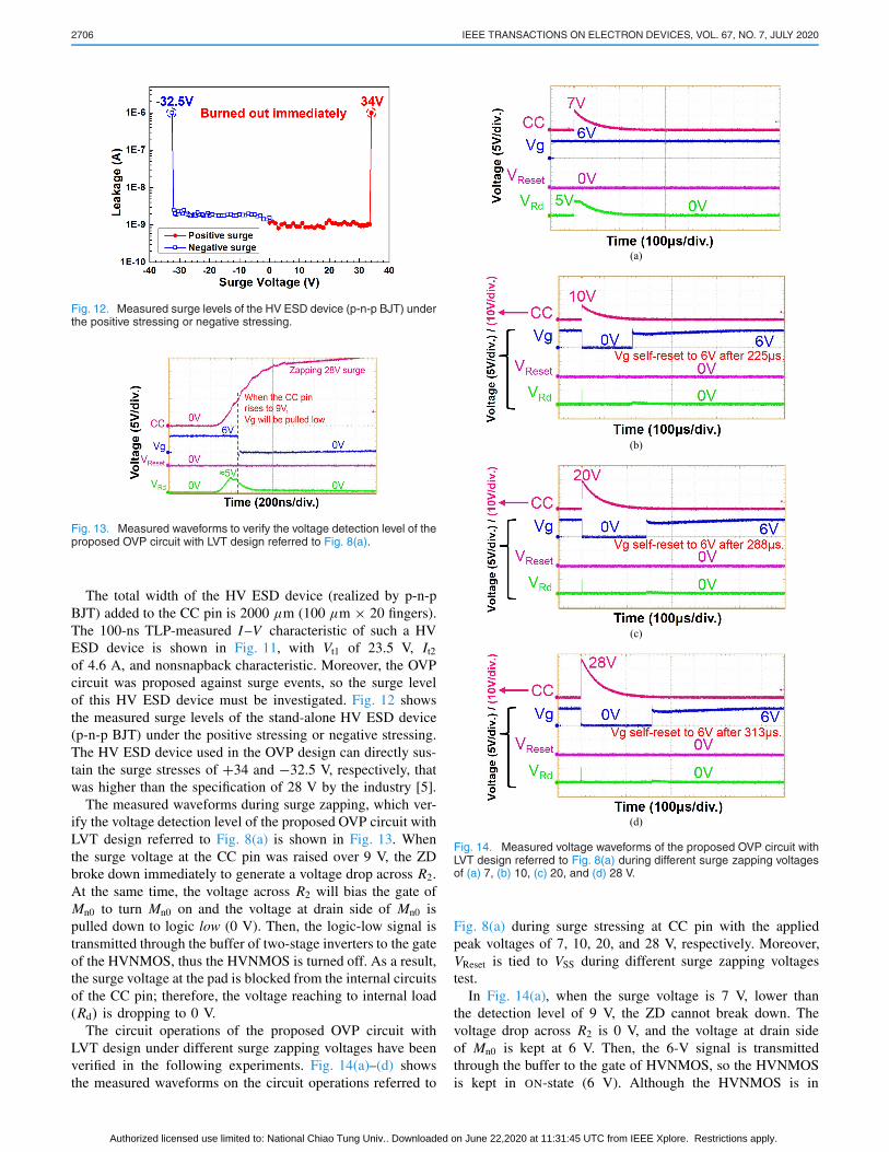
To investigate the HCD carrier reliability with surge impactson the HVNMOS, the device was stressed by the surge voltagewaveform of many times (up to 10 000 times) with 28-Vzapping voltage, where the calibrated 1.2/50-μs open-circuitsurge voltage waveform with a 28-V zapping voltage canbe referred to Fig. 1. The surge peak voltage was chosento be 28 V, corresponding to the specification used in theindustry [5]. Fig. 3 shows the measured waveform of thecontinuous surge voltage cycles used in the device-level HCDtest. The overstress cycles are 5000 and 10 000 times, andthe interval time of each surge voltage cycle is 1 s. Thedevice cross-sectional view of a stand-alone HVNMOS for
Fig. 3. Measured voltage waveform of the continuous surge cycles usedin the device-level HCD test.
Fig. 4. Device cross-sectional view of the 30-V HVNMOS used for thedevice-level HCD test.
Fig. 5. Schematic of measurement set-up for the device-level HCD testby surge cycles.
the test is shown in Fig. 4, which was fabricated in a 0.15-μmBCD technology. The surge voltage patterns were applied tothe drain of stand-alone HVNMOS device with its sourcegrounded, as well as its gate was biased at 6 and 0 V undersurge test, respectively, and the schematic illustrating the testset-up is shown in Fig. 5.
B. Measurement Results of the HVNMOSAfter the HCD Test
After the continuous surge voltage cycles test, the I–Vcurves and some electrical parameters of the standalone HVN-MOS are remeasured and compared to seek the degradationdue to surge stress.
First, the Id − Vd characteristics of the HVNMOS after thesurge tests of 5000 and 10 000 times under Vg biases of 6and 0 V were shown in Fig. 6(a) and (b), respectively. Theinsets in Fig. 6(a) and (b) were the zoomed-in parts on thelinear region of the Id−Vd characteristics. Surge stresses reallycaused degradation on HVNMOS under the gate voltage (Vg)of 6 V. On the contrary, there is no obvious change after surgestresses on the HVNMOS under Vg of 0 V.
Furthermore, single point measurement was also carried outto obtain Idlin (Vd of 0.1 V, Vg of 6 V) of the HVNMOS,
Authorized licensed use limited to: National Chiao Tung Univ.. Downloaded on June 22,2020 at 11:31:45 UTC from IEEE Xplore. Restrictions apply.
2704 IEEE TRANSACTIONS ON ELECTRON DEVICES, VOL. 67, NO. 7, JULY 2020
Fig. 6. Measured Id − Vd characteristics of the stand-alone HVNMOSafter surge stresses of 5000 and 10000 times under Vg of (a) 6 and(b) 0 V.
in the early linear region. In Fig. 7(a), the degradation of Idlin
of the HVNMOS, which was tested under Vg of 6 V aftersurge stressing of 5000 and 10 000 times, is more seriousthan that under Vg of 0 V. Surge stresses really caused Idlin
degradation of ∼26% on the HVNMOS that stressed under Vg
of 6 V. Finally, the threshold voltage (Vth) and maximum trans-conductance (Gm,max) is derived from the measured Id −Vg
characteristics. The shifting percentages of Vth and Gm,max onthe HVNMOS after surge stresses of 5000 and 10 000 timesunder Vg biases of 6 and 0 V are shown in Fig. 7(b) and (c),respectively. Surge stresses really caused 1.6% increment onVth of the HVNMOS that stressed under Vg of 6 V after10 000 times stressing, and that stressed under Vg of 0 Vshowed no change almost. The degradation of Gm,max onthe HVNMOS that stressed under Vg of 6 V after surgestressing of 5000 and 10 000 times is more serious than thatstressed under Vg of 0 V. As shown in Fig. 7(c), surge stressescaused degradation of ∼9.7% on the Gm,max of HVNMOS thatstressed under Vg of 6 V after 10 000 times surge stressing.
Therefore, the on-chip OVP circuit is strongly requested toprevent HVNMOS against surge events and HCD degradationfor using in the CC pin of USB type-C interface IC.
III. SURGE OVP CIRCUIT
A. Design Consideration
The schematic diagrams of the proposed OVP circuits wereshown in Fig. 8(a) and (b). In order to limit the overstress
Fig. 7. Shifting percentages of (a) Idlin, (b) Vth, and (c) Gm,max of theHVNMOS after surge stresses of 5000 and 10000 times under Vg of6 and 0 V, respectively.
voltage entering into the CC pin of USB type-C IC, HVNMOSmust be used as a pass transistor at the CC pin and thesize of the HVNMOS should be large enough to drive theoutput current (at least 200 mA) in the condition of VCONN
mode, which is a specified operation of USB Type-C interface.Furthermore, there is a function of the CC pin called dual roleport, which allows the CC pin to be downstream facing port(source port) or upstream facing port (sink port) according tothe system protocol.
Owing to surge currents passing through the triggering pathof the detection circuit, it is essential to limit the currentflowing into the Zener diode (ZD). As a result, current-limitingresistors R1 and R2 are added on the triggering path to avoidthe ZD getting burned out immediately during surge events.
Authorized licensed use limited to: National Chiao Tung Univ.. Downloaded on June 22,2020 at 11:31:45 UTC from IEEE Xplore. Restrictions apply.
KE AND KER: ON-CHIP OVP DESIGN AGAINST SURGE EVENTS ON THE CC PIN OF USB TYPE-C INTERFACE 2705
Fig. 8. Proposed OVP circuits to detect the overstress events with (a) oneZD and (b) two ZDs in stacked configuration.
TABLE IDEVICE DIMENSIONS USED IN THE PROPOSED OVP STRUCTURES
Meanwhile, the ZD should be suitably sizing large enough toguarantee self-protection under surge stresses.
The gate voltage of HVNMOS should be pulled to 0 Vduring surge zapping. The ZD in the OVP circuit is usedto detect the overstress voltage level zapping to the CCpin. Different over-voltage detection levels can be achievedby different stacked number of ZDs, those are called aslower voltage trigger (LVT) and higher voltage trigger (HVT)designs in this work.
When the voltage of the CC pin is in normal operatingvoltage (5 V), the node of Vg is set to 6 V, and the HVNMOSis in ON-state to pass the signal into the interface circuit.When the overstress voltage onto the CC pin is high enough,the circuit is triggered to pull down the node of Vg to 0 V;therefore, the HVNMOS is in OFF-state to prevent the over-stress voltage and large current entering into the interfacecircuit. Furthermore, a positive feedback which is composedof Mn0, Mp0, R2, and R3 is used to enhance the turn-off timeof the HVNMOS during surge events.
An on-chip HV ESD device is necessary to be added to theCC pin to clamp the overstress from ESD and surge events.The ESD device with nonsnapback characteristic is neededto avoid the latch-up-like issue during surge events, whenthe zapping voltage is higher than the trigger voltage (Vt1)of the device. As a result, the Vt1 and holding voltage (Vh)of the HV ESD device is selected higher than the normaloperating voltage (5 V), but lower than the breakdown voltageof the pass transistor (HVNMOS). In summary, the designparameters of the devices among the proposed OVP structuresare listed in Tables I and II. The difference between OVPcircuits with LVT and HVT designs is only the stacked numberof ZDs.
B. Measurement Results of OVP Circuit With LVT Design
The proposed OVP circuits have been fabricated in a0.15-μm BCD technology. The die photograph of the proposed
TABLE IIRESISTORS AND ESD DEVICE USED IN THE
PROPOSED OVP STRUCTURES
Fig. 9. Die photo of the proposed OVP circuit with LVT design.
Fig. 10. Measured voltage waveforms of a 5-V sine wave passingthrough the HVNMOS of the OVP circuit into the CC pin referred toFig. 7(a) with LVT design.
Fig. 11. Measured TLP I–V characteristic of the HV ESD device[p-n-p bipolar junction transistor (BJT)] added to the CC pin.
OVP circuit with LVT design is shown in Fig. 9. First of all,the normal operating voltage of CC pin in USB type-C iswithin 0–5 V. Fig. 10 shows the measured voltage waveformsof a 5-V sine wave successfully passing through the OVPcircuit with LVT design from the CC pin to the internal loadof 5.1-k� resistor (Rd), as referred to the circuit of Fig. 8(a).
Authorized licensed use limited to: National Chiao Tung Univ.. Downloaded on June 22,2020 at 11:31:45 UTC from IEEE Xplore. Restrictions apply.
2706 IEEE TRANSACTIONS ON ELECTRON DEVICES, VOL. 67, NO. 7, JULY 2020
Fig. 12. Measured surge levels of the HV ESD device (p-n-p BJT) underthe positive stressing or negative stressing.
Fig. 13. Measured waveforms to verify the voltage detection level of theproposed OVP circuit with LVT design referred to Fig. 8(a).
The total width of the HV ESD device (realized by p-n-pBJT) added to the CC pin is 2000 μm (100 μm × 20 fingers).The 100-ns TLP-measured I–V characteristic of such a HVESD device is shown in Fig. 11, with Vt1 of 23.5 V, It2
of 4.6 A, and nonsnapback characteristic. Moreover, the OVPcircuit was proposed against surge events, so the surge levelof this HV ESD device must be investigated. Fig. 12 showsthe measured surge levels of the stand-alone HV ESD device(p-n-p BJT) under the positive stressing or negative stressing.The HV ESD device used in the OVP design can directly sus-tain the surge stresses of +34 and −32.5 V, respectively, thatwas higher than the specification of 28 V by the industry [5].
The measured waveforms during surge zapping, which ver-ify the voltage detection level of the proposed OVP circuit withLVT design referred to Fig. 8(a) is shown in Fig. 13. Whenthe surge voltage at the CC pin was raised over 9 V, the ZDbroke down immediately to generate a voltage drop across R2.At the same time, the voltage across R2 will bias the gate ofMn0 to turn Mn0 on and the voltage at drain side of Mn0 ispulled down to logic low (0 V). Then, the logic-low signal istransmitted through the buffer of two-stage inverters to the gateof the HVNMOS, thus the HVNMOS is turned off. As a result,the surge voltage at the pad is blocked from the internal circuitsof the CC pin; therefore, the voltage reaching to internal load(Rd) is dropping to 0 V.
The circuit operations of the proposed OVP circuit withLVT design under different surge zapping voltages have beenverified in the following experiments. Fig. 14(a)–(d) showsthe measured waveforms on the circuit operations referred to
Fig. 14. Measured voltage waveforms of the proposed OVP circuit withLVT design referred to Fig. 8(a) during different surge zapping voltagesof (a) 7, (b) 10, (c) 20, and (d) 28 V.
Fig. 8(a) during surge stressing at CC pin with the appliedpeak voltages of 7, 10, 20, and 28 V, respectively. Moreover,VReset is tied to VSS during different surge zapping voltagestest.
In Fig. 14(a), when the surge voltage is 7 V, lower thanthe detection level of 9 V, the ZD cannot break down. Thevoltage drop across R2 is 0 V, and the voltage at drain sideof Mn0 is kept at 6 V. Then, the 6-V signal is transmittedthrough the buffer to the gate of HVNMOS, so the HVNMOSis kept in ON-state (6 V). Although the HVNMOS is in
Authorized licensed use limited to: National Chiao Tung Univ.. Downloaded on June 22,2020 at 11:31:45 UTC from IEEE Xplore. Restrictions apply.

KE AND KER: ON-CHIP OVP DESIGN AGAINST SURGE EVENTS ON THE CC PIN OF USB TYPE-C INTERFACE 2707
Fig. 15. Measured voltage waveforms of the OVP circuit operation whena 6-V reset signal is given after the 28-V surge zapping on the CC pin.
ON-state during 7-V surge stress, the peak voltage enteringinto the internal load (Rd) is limited by the HVNMOS to only∼5 V, which is the nominal voltage of the CC pin in USBtype-C interface. Because the Vth of the HVNMOS is around1 V, in order to keep the HVNMOS in ON-state theoretically,the maximum voltage drop at the source side is equal to“Vg − Vth.” Thus, the internal circuits of the CC pin can beprevented from overstress.
In Fig. 14(b), when the surge voltage is 10 V, higher thanthe detection level of 9 V, the ZD broke down. Meanwhile,it generates a voltage drop across R2 to turn on Mn0 on andthe voltage at drain side of Mn0 is pulled down to logic low(0 V). Because the drain side of Mn0 is pulled down to logiclow, there is a voltage drop across R3 biasing the gate of Mp0
to turn Mp0 on. As a result, a positive feedback is generatedwith Mn0 and Mp0 both in ON-state to lock the detection resultof a surge event for a long time. Finally, the logic-low signalis transmitted through buffer to the gate of the HVNMOS,and the HVNMOS is turned off for 225 μs, which is longenough during surge events because the maximum energy ofsurge events is always within ∼50 μs. With sufficient turn-offtime, the robustness against HCD can be improved efficiently.Moreover, the internal circuits of the CC pin can be preventedfrom being damaged by surge events, as the voltage reachingto internal load (Rd) is dropping to 0 V during the whole surgeevent.
As shown in Fig. 14(c) and (d) with the surge voltagesof 20 and 28 V, respectively, higher than the detection levelof 9 V, the ZD broke down as well to enable the detectionfunction of the OVP circuit. Therefore, the mechanism of thecircuit operation is the same as that under the surge voltage of10 V. However, it is worth mentioning that the turn-off times ofthe HVNMOS are different among the zapping voltages of 10,20, and 28 V, which are 225, 288, and 313 μs, respectively.With the higher surge zapping voltage, the longer turn-off timeof the HVNMOS can be achieved, which can be ascribed tothe fact that the higher zapping energy can keep the positivefeedback to maintain for longer time.
Finally, the reset function of the proposed OVP circuitwith LVT design has been also verified and the measuredvoltage waveforms are shown in Fig. 15. First, a 28-V surgevoltage is applied to the CC pin and the positive feedbackis generated to lock the gate voltage (Vg) of HVNMOS
Fig. 16. Measured voltage waveforms of a 5-V sine wave passingthrough the HVNMOS of the OVP circuit into the CC pin referred toFig. 8(b) with HVT design.
Fig. 17. Measured waveforms to verify the voltage detection level of theproposed OVP circuit with HVT design referred to Fig. 8(b).
at 0 V. Later than the surge zapping (after 200 μs), a 6-V resetsignal (VReset) is added to the gate of Mpr which interruptsthe positive feedback. When the gate of Mpr is applied by6-V reset signal, its Vgs becomes 0 V to turn itself off. As aconsequence, the voltage at drain side of Mn0 is repulledup to 6 V. The 6-V signal is transmitted through the bufferto the gate of HVNMOS and the HVNMOS is retuned inON-state. Therefore, the voltage (VRd) on the internal load(Rd) was followed with the residual surge voltage on the CCpin at the same time.
C. Measurement Results of OVP Circuit With HVTDesign
Two ZDs were stacked in the OVP circuit of HVT design toget a higher triggering voltage. It can make the triggering pathstronger against EOS events and make the OVP circuit possessbetter reliability. Fig. 16 shows the measured waveforms of a5-V sine wave successfully passing through the OVP circuitwith HVT design from the CC pin to the internal load of5.1-k� resistor (Rd), referred to the circuit in Fig. 8(b). TheHV ESD device (p-n-p BJT) is the same as that used in theLVT design with a Vt1 of 23.5 V.
The measured voltage waveforms to verify the voltagedetection level of the proposed OVP circuit with HVT designduring surge zapping is shown in Fig. 17. When the surgevoltage at the CC pin was raised over 16 V, the ZD brokedown immediately to generate a voltage drop across R2. At thesame time, the voltage across R2 turn Mn0 on and the voltage
Authorized licensed use limited to: National Chiao Tung Univ.. Downloaded on June 22,2020 at 11:31:45 UTC from IEEE Xplore. Restrictions apply.

2708 IEEE TRANSACTIONS ON ELECTRON DEVICES, VOL. 67, NO. 7, JULY 2020
Fig. 18. Measured voltage waveforms of the proposed OVP circuit withHVT design referred to Fig. 8(b) during different surge zapping voltagesof (a) 10, (b) 20, and (c) 28 V.
at drain side of Mn0 is pulled down to logic low (0 V). Then,the logic-low signal is transmitted through the buffer to thegate of the HVNMOS; therefore, the HVNMOS is turned off.As a result, the surge voltage is blocked from the internalcircuits of the CC pin, so the voltage reaching to internal load(Rd) is dropping to 0 V.
In Fig. 18(a), when the surge voltage is 10 V, lower thanthe detection level of 16 V, the ZD cannot break down. Thevoltage drop across R2 is 0 V, and the voltage at drain sideof Mn0 is still kept in 6 V. Therefore, the HVNMOS is stillkept in ON-state. Although the HVNMOS is in ON-state during10-V surge stress, the peak voltage entering into the internalload (Rd) is limited by the HVNMOS to ∼5 V which is thenominal voltage of the CC pin in USB type-C interface. Thus,the internal circuits of the CC pin can be prevented from beingdamaged by surge overstress.
In Fig. 18(b), when the surge voltage is 20 V, higher thanthe detection level of 16 V, the ZD broke down to generate a
Fig. 19. Schematic of the OVP circuit for the investigation of self-resetphenomenon.
voltage drop across R2 to turn Mn0 on. The voltage at drainside of Mn0 is pulled down to logic low and a voltage dropacross R3 biasing the gate of Mp0 to turn Mp0 on. As aresult, a positive feedback is generated with Mn0 and Mp0
both in ON-state to lock the detection result for a long time.Therefore, the voltage at drain side of Mn0 can be pulleddown to logic low for sufficiently long time as well. Finally,the logic-low signal is transmitted to the gate of the HVNMOSand the HVNMOS is turned off for 526 μs, which is longenough during surge events, because the maximum energy ofsurge events is within ∼50 μs. With sufficient turn-off time,the HCD robustness can be improved efficiently. Moreover,the internal circuits of the CC pin can be prevented from beingdamaged by surge events, and the voltage reaching to internalload (Rd) is dropping to 0 V during the whole surge event.
In Fig. 18(c), with the surge voltage of 28 V, higher thanthe detection level of 16 V, the ZD broke down as well.Therefore, the mechanism of the circuit operation is the sameas that under the surge voltage of 20 V. However, it isworth mentioning that the turn-off times of the HVNMOS aredifferent between surge zapping voltage of 20 and 28 V, whichare 526 and 608 μs, respectively. The higher zapping voltage,the longer turn-off time of HVNMOS can be achieved, whichcan be ascribed to the fact that the higher zapping energy cankeep the positive feedback for longer time.
The reset function of the proposed OVP circuit with HVTdesign has also been verified, and the measured voltagewaveforms are the same as those shown in Fig. 15. The resetfunction is provided to early remove the lock state of detectionresult for system control with feasible applications. If noadditional control signal applied to the reset node, its normalbias is kept at 0 V to enable the OVP circuit function and thereset function will be automatically executed by OVP circuititself.
IV. DISCUSSION
To investigate the self-reset mechanism in the OVP circuit,the following experiments had been done to investigate the rootcause of self-reset. In Fig. 19, by adding an external diodeoutside the bond pad of CC pin, when the surge voltage ishigher than the detection level, the gate voltage (Vg) of the
Authorized licensed use limited to: National Chiao Tung Univ.. Downloaded on June 22,2020 at 11:31:45 UTC from IEEE Xplore. Restrictions apply.

KE AND KER: ON-CHIP OVP DESIGN AGAINST SURGE EVENTS ON THE CC PIN OF USB TYPE-C INTERFACE 2709
Fig. 20. Measured voltage waveforms of the proposed OVP circuit withan external diode outside the bond pad of the CC pin during 28-V voltagesurge zapping.
HVNMOS can be pulled to logic low for the whole residualtime, as the measured waveforms shown in Fig. 20. As a result,the self-reset phenomenon can be ascribed to the leakage pathwith the yellow dotted line shown in Fig. 19. When there isan extra diode adding into the triggering path (R1, ZD, andR2), the current in the positive feedback cannot leak throughthe yellow dotted line to the pad after the surge events. As aresult, the positive feedback can always be kept to further keepthe HVNMOS in OFF-state. Therefore, the ON-resistance alongthe devices on the yellow dotted line (Mpr , Mp0, ZD, and R1)and the latch strength (formed by Mp0, R3, Mn0, and R2) candecide the minimum “self-reset time” of the OVP circuit.
Because the normal operating voltage of the CC pin is5 V, it is recommended to design the minimum “self-resettime” which is the timing when the voltage of the CC pinis dropping to 5 V. Such a desired “self-reset time” can bewell adjusted by additional circuit design with SimulationProgram with Integrated Circuit Emphasis (SPICE) simulationon the device dimensions (Mp0, Mn0, Mpr , and ZD) and theresistors (R3, R2, and R1) in the latch loop. For more precisionoperation on the rest time to restart the OVP circuit backto its original detection mode, the Vg signal of the OVPcircuit can be used to trigger a digital timing circuit with theselected/desired reset time, and then the digital timing circuitsends out a signal (logic high) to the node of VReset to turnMpr off. Therefore, the latch mode in the OVP circuit can bereleased earlier by the additional digital timing circuit with aprecision timing control for applications.
V. CONCLUSION
Different from the measurement on HCD by dc stress,this work has verified that HCD issue on HVNMOS indeedhappened by ac stress, such as surge events, especially whenthe HVNMOS was kept at ON-state. Based on the device-levelHCD test results under surge stresses, the HVNMOS toprevent the internal circuits of the CC pin against surge eventsneeds an over-voltage detector to detect surge events and thento turn the HVNMOS off when surge events happen on theCC pin. Different over-voltage detection levels of the proposedOVP circuit can be achieved by ZDs with different stacked
numbers. A positive feedback in the OVP circuit is used tolock the detection result for a longer time. Moreover, a resetfunction is also provided to early remove the lock state ofdetection result for feasible control in system applications.The proposed OVP circuit has been successfully verified ina 0.15-μm BCD technology, which can be fully on-chipintegrated into the USB type-C IC products to enhance therobustness against surge events.
ACKNOWLEDGMENT
The authors thank Jian-Hsing Lee, Shao-Chang Huang,Yeh-Ning Jou, Chih-Hsuan Lin, Li-Fan Chen, Ting-You Lin,Hsien-Feng Liao, Hwa-Chyi Chiou, Yeh-Jen Huang, andChun-Chih Chen of the Device Engineering Division, VIS,for their valuable technical suggestions. The chip fabricationwas supported by Vanguard International Semiconductor Cor-poration (VIS), Taiwan.
REFERENCES
[1] Universal Serial Bus 3.1 Specification, USB Implementers Forum,Beaverton, OR, USA, 2013.
[2] Universal Serial Bus Type-C Cable and Connector Specification, USBImplementers Forum, Beaverton, OR, USA, 2019.
[3] Electromagnetic Compatibility (EMC)—Part 4–5: Testing and Measure-ment Techniques—Surge Immunity Test, Standard IEC 61000-4-5, 2014.
[4] X. Liu, A. Yazdi, S. Kwaaitaal, C. Speelman, and X. Zhang, “Voltageclamp circuit for surge protection,” U.S. Patent 20 190 020 194 A1,Jan. 17, 2019.
[5] H. I. Oporta, S. P. Mane, T. O’Brien, and C. G. Sporck, “Over-voltage protection systems and methods,” U.S. Patent 10 431 939 B2,Oct. 1, 2019.
[6] P. Mondal, A. Khamesra, and H. P. Vispute, “Overvoltage protectionfor universal serial bus type-C (USB-C) connector systems,” U.S. Patent10 218 129 B1, Feb. 26, 2019.
[7] N. A. Bodnaruk and D. W. Mattos, “Voltage protection for universal ser-ial bus type-C (USB-C) connector systems,” U.S. Patent 10 381 787 B1,Aug. 13, 2019.
[8] S.-E. Liu, H.-S. Huang, Y.-H. Lin, and M.-T. Lin, “Interface circuits tomonitor and prevent overstress damage,” U.S. Patent 20 180 102 639 A1,Apr. 12, 2018.
[9] S. E. Liu et al., “Type-C interface reliability concern of electricaloverstress and design for mitigation,” in Proc. IEEE Int. Rel. Phys.Symp. (IRPS), Apr. 2017, pp. 3A-5.1–3A-5.4, doi: 10.1109/IRPS.2017.7936280.
[10] D. Varghese et al., “Off-state degradation in drain-extended NMOS tran-sistors: Interface damage and correlation to dielectric breakdown,” IEEETrans. Electron Devices, vol. 54, no. 10, pp. 2669–2678, Oct. 2007, doi:10.1109/TED.2007.904587.
[11] D. Varghese, H. Kufluoglu, V. Reddy, H. Shichijo, S. Krishnan, andM. A. Alam, “Universality of off-state degradation in drain extendedNMOS transistors,” in IEDM Tech. Dig., Dec. 2006, pp. 1–4, doi: 10.1109/IEDM.2006.346895.
[12] K. M. Wu et al., “Effects of gate bias on hot-carrier reliability indrain extended metal-oxide-semiconductor transistors,” Appl. Phys. Lett.,vol. 89, no. 18, Oct. 2006, Art. no. 183522, doi: 10.1063/1.2374881.
[13] J. F. Chen, K.-M. Wu, K.-W. Lin, Y.-K. Su, and S. L. Hsu, “Hot-carrierreliability in submicrometer 40V LDMOS transistors with thick gateoxide,” in Proc. Int. Rel. Phys. Symp., Apr. 2005, pp. 560–564, doi: 10.1109/RELPHY.2005.1493148.
[14] R. Versari and A. Pieracci, “Experimental study of hot-carrier effectsin LDMOS transistors,” IEEE Trans. Electron Devices, vol. 46, no. 6,pp. 1228–1233, Jun. 1999, doi: 10.1109/16.766890.
Authorized licensed use limited to: National Chiao Tung Univ.. Downloaded on June 22,2020 at 11:31:45 UTC from IEEE Xplore. Restrictions apply.