outline motivation - university of washingtonfaculty.washington.edu/manisoma/ee540/dft.pdf · soma...
TRANSCRIPT
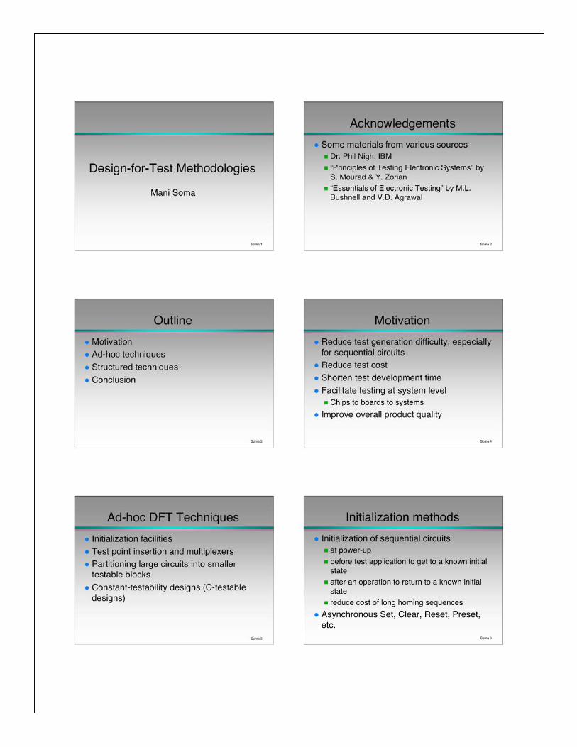
Soma 1
Design-for-Test Methodologies
Mani Soma
Soma 2
Acknowledgements
Some materials from various sourcesDr. Phil Nigh, IBM
“Principles of Testing Electronic Systems” byS. Mourad & Y. Zorian“Essentials of Electronic Testing” by M.L.Bushnell and V.D. Agrawal
Soma 3
Outline
MotivationAd-hoc techniquesStructured techniquesConclusion
Soma 4
Motivation
Reduce test generation difficulty, especiallyfor sequential circuitsReduce test costShorten test development timeFacilitate testing at system level
Chips to boards to systems
Improve overall product quality
Soma 5
Ad-hoc DFT Techniques
Initialization facilitiesTest point insertion and multiplexersPartitioning large circuits into smallertestable blocksConstant-testability designs (C-testabledesigns)
Soma 6
Initialization methods
Initialization of sequential circuitsat power-up
before test application to get to a known initialstateafter an operation to return to a known initialstate
reduce cost of long homing sequences
Asynchronous Set, Clear, Reset, Preset,etc.
Soma 7
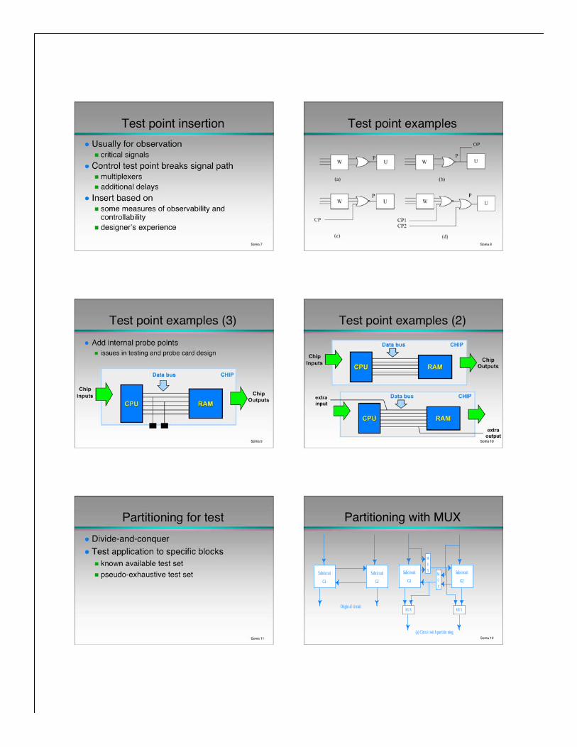
Test point insertion
Usually for observationcritical signals
Control test point breaks signal pathmultiplexersadditional delays
Insert based onsome measures of observability andcontrollabilitydesigner s experience
Soma 8
Test point examples
Soma 9
Test point examples (3)
Add internal probe pointsissues in testing and probe card design
CPUCPU RAMRAM
Chip
Inputs Chip
Outputs
Data busData bus CHIPCHIP
Soma 10
Test point examples (2)
CPUCPU RAMRAM
Chip
InputsChip
Outputs
Data busData bus CHIPCHIP
CPUCPU RAMRAM
Data busData bus CHIPCHIPextraextra
inputinput
extraextra
outputoutput
Soma 11
Partitioning for test
Divide-and-conquerTest application to specific blocks
known available test setpseudo-exhaustive test set
Soma 12
Partitioning with MUX
(a) Circui t wit h par titio ning
Subcircuit
G1
MU X
M
U
X Subcircuit
G2
M
U
X
MU XOrigin al ci rcuit
Subcircuit
G1
Subcircuit
G2
Soma 13
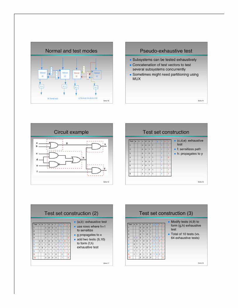
Normal and test modes
(b) Nor mal mod e
Subcircuit
G1
MU X
M
U
XSubcircuit
G2
M
U
X
MU X
(c) Tes t mode for subc ircu it G1
Subcircuit
G1
MU X
M
U
X Subcircuit
G2
M
U
X
MU X
Soma 14
Pseudo-exhaustive test
Subsystems can be tested exhaustivelyConcatenation of test vectors to testseveral subsystems concurrentlySometimes might need partitioning usingMUX
Soma 15
Circuit example
Soma 16
Test set construction
1111118
1110117
1111016
1110015
0011104
1110103
1111002
1110001
yxhgfedcbaTest (c,d,e): exhaustivetest
f: sensitizes pathh: propagates to y
Soma 17
Test set construction (2)
(a,b): exhaustive test
use rows where h=1to sensitizeg propagates to xadd two tests (9,10)to form (f,h)exhaustive test
01000010
0001109
11111111118
11111011017
11111101106
10101001005
0011104
1110103
1111002
1110001
yxhgfedcbaTest
Soma 18
Test set construction (3)
Modify tests (4,9) toform (g,h) exhaustivetest
Total of 10 tests (vs.64 exhaustive tests)
01000010
00010110109
11111111118
11111011017
11111101106
10101001005
00001110004
1110103
1111002
1110001
yxhgfedcbaTest

Soma 19
C-testable designs
Iterative Logic Arrays (ILA)structured designs using arrays of identicalcells
adders, multipliers, etc.RAMFPGAbit-slice processors
Array test set based on cell test setC-testable: array test set size is independent ofnumber of cells in array
Soma 20
ILA structures
1-dimensional
i-1 i i+1
2-dimensional
i,j
Soma 21
Full adder example
i+1 i i-1
Xi Yi
Co Ci
Si
6 tests with identical carryvalues2 alternate-cell tests withopposite carry values
total = 8 tests
11111
01011
01101
10001
01110
10010
10100
00000
SiCoCiYiXi
Soma 22
Structured DFT Techniques
Scan dominates digital DFTClassical scan
Boundary scan
IDDQ design guidelinesBuilt-in Self Test (BIST) techniques
in other lectures
Soma 23
Scan concept
Combinational circuit
X1
X2X3
Z1
Z2
Z3
CLK
D D DQ Q Q
X1
X2
X3
Combinational circuit
CLK
D D DQ Q
Q
SE
SISO
Z1
Z2Z3
Soma 24
LSSD system diagram
Soma 25
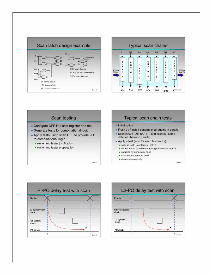
Scan latch design example
D: normal data in
CK: system clock
Q: normal latch output
SDI: scan data in
SCKA, SCKB: scan clocks
SDO: scan data out
Soma 26
Typical scan chains
CC
HH
AA
II
NN
11
CC
HH
AA
II
NN
22
CC
HH
AA
II
NN
66
CC
HH
AA
II
NN
77
CC
HH
AA
II
NN
33
CC
HH
AA
II
NN
55
CC
HH
AA
II
NN
44
SO1SO1 SO2SO2 SO4SO4SO3SO3 SO5SO5 SO6SO6 SO7SO7
primaryprimaryinputsinputs
primaryprimaryoutputsoutputs
SI1SI1 SI2SI2 SI3SI3 SI5SI5 SI6SI6 SI7SI7SI4SI4
Soma 27
Scan testing
Configure DFF into shift register and testGenerate tests for combinational logicApply tests using scan DFF to provide I/Oto combinational logic
easier and faster justificationeasier and faster propagation
Soma 28
Typical scan chain tests
Initialization
Flush 0 / Flush 1 patterns of all chains in parallelScan in 001100110011… and scan out samedata, all chains in parallelApply a test (loop for each test vector)
scan in test 1 (contents of D FF)
set up inputs (combinational logic inputs for test 1)
exercise system clock once
scan out contents of D FF
check scan outputs
Soma 29
PO strobe
PI stim
PI-PO delay test with scan
C1 system
clock
C2 system/scan
clock
Soma 30
PO strobe
C1 system
clock
C2 system/scan
clock
PI stim
L2-PO delay test with scan

Soma 31
PO strobe
PI stim
L2-L1 delay test with scan
C1 system
clock
C2 system/scan
clock
Soma 32
Scan design rules
All latches must be scannable (full-scan)Every latch must be on a scan path
There may be multiple scan paths
Non-overlapping clocks
No gating between clocksAll clocks must be primary inputsSDI and SDO must be primary I/O
Soma 33
Scan design advantages
Testable sequential systemsTest scan path using DFF tests
Ease of testing remaining combinationallogic
Access to internal nodes via scan
Fast test generation (all combinational)Ease of delay testing of combinationalblocks
Soma 34
Scan design advantages (2)
Complete controllability of all registersComplete observability of all registersCombinational logic test generationUse cheaper test systems
Additional diagnostic capability
Soma 35
Scan design cost
More complex designarea: 2 - 15%
Additional delayPossible to minimize by clever designs
More I/O required (1-3 pins)Recover cost as part of system test facilities
Slow test (not at speed)Time to scan long paths seriallyLarger wiring parasitics
Soma 36
ATPG Example: S5378
Original
2,781
179 0
0.0% 4,603
35/49 70.0%
70.9% 5,533 s
414 414
Full-scan
2,781
0 179
15.66% 4,603
214/228
99.1% 100.0%
5 s 585
105,662
Number of combinational gatesNumber of non-scan flip-flops (10 gates each)
Number of scan flip-flops (14 gates each)Gate overhead
Number of faultsPI/PO for ATPG
Fault coverageFault efficiency
CPU time on SUN Ultra II, 200MHz processorNumber of ATPG vectors
Scan sequence length

Soma 37
Scan varieties
Full-scan: increasing usepartitioning issues in multiple scan chainsoptimal placement of DFF in scan chain
Partial-scanRandom-access scan
Individual latch addressableHigh overhead
Level-Sensitive Scan DesignNo races and timing problems
Soma 38
Partial Scan ExampleCircuit: TLC, 355 gates, 21 flip-flops
Scan Max. cycle Depth* ATPG Fault sim. Fault ATPG Test seq.
flip-flops length CPU s CPU s cov. vectors length
0 4 14 1,247 61 89.01% 805 805
4 2 10 157 11 95.90% 247 1,249
9 1 5 32 4 99.20% 136 1,382
10 1 3 13 4 100.00% 112 1,256
21 0 0 2 2 100.00% 52 1,190
* Cyclic paths ignored
Soma 39
Test Length StatisticsCircuit: TLC
200
100
00 50 100 150 200 250
Num
ber
of
fault
s
200
100
00 5 10 15 20 25
Num
ber
of
fault
s
200
100
00 5 10 15 20 25
Num
ber
of
fault
s
Without scan
9 scan flip-flops
10 scan flip-flops
Test
length
Test
length
Test
length
Soma 40
Partial vs. Full Scan: S5378
Original
2,781
179
0
0.0%
4,603 35/49
70.0% 70.9%
5,533 s
414 414
Full-scan
2,781
0
179
15.66%
4,603214/228
99.1% 100.0%
5 s
585105,662
Number of combinational gates
Number of non-scan flip-flops (10 gates each)
Number of scan flip-flops (14 gates each)
Gate overheadNumber of faults
PI/PO for ATPGFault coverage
Fault efficiencyCPU time on SUN Ultra II
200MHz processorNumber of ATPG vectors
Scan sequence length
Partial-scan
2,781
149
30
2.63% 4,603
65/79 93.7%
99.5% 727 s
1,117
34,691
Soma 41
Motivation for board test
High-density boards / Multichip Modules(MCM) not testable using bed-of-nailsBoard failure modes:
stuck-at faultsopenshorts
incorrect components
Lack of test access
Soma 42
Bed-of-nails testing

Soma 43
Boundary Scan standard
IEEE 1149.1JTAG (Joint Test Activity Group)
First release: 1990under revisions
Facilities to test for board failuresoptional instructions for internal IC testingusable in system-level tests
Many ICs now incorporate 1149.1
Soma 44
Boundary Scan topology
Soma 45
Boundary Scan cell
At chip I/O onlyElectronic access to each chip pin
TDI
Update DR
TDO
Q
QSET
CLR
D
ClockDR
Mode
1
0
Q
QSET
CLR
D
0
1
Data_In
Q
QSET
CLR
D
Q
QSET
CLR
D1
2
ShiftDR
Data_Out
Soma 46
Test access port (TAP)
Device ID. Register
Bypass Register
Instruction Register (IR)
TDI
TDO
Bo
un
dar
y
Scan
Reg
isters
Controller
TDM TDK
TMS
TCKTDITDO
optionalTRST(reset)
Soma 47
TAP registers
Bypass registerremoves chip from boundary scan path
faster test application
Instruction registermandatory instruction: Bypass, Extest, Sample/ Preload
optional instruction: Intest, Idcode, RunBist,Clamp, HighZ
Soma 48
TAP controller
Simple state machine
Load instructionLoad test dataExecute test
Unload (shift-out) testresultsInitialization

Soma 49
Register operations
Instruction registersloaded serially for all ICs
captured in parallel to each IC
Data registers at chip pinsloaded serially, captured in parallel
test data and test results
Soma 50
Instruction scan
TMS
TCK
Tes
t-L
ogic
-R
eset
Sele
ct-I
R--
Scan
Ru
n-T
est/
Idle
Sele
ct-D
R--
Scan
Cap
ture
-IR
Shif
t-IR
Exi
t1-I
R
Shif
t-IR
Pau
se-I
R
Exi
t2-I
R
Exi
t1-I
R
Up
dat
e-IR
Ru
n-T
est/
IdleController
State
Data inputto IR
TDI
IR shift-register
Paralleloutput of IR
Data inputto TDR
TDR shift-register
Paralleloutput of
TDR
Registerselected
TDO enable
TDO
Inactive Active Inactive Active Inactive
Instruction register
Old data
NewInstruction
IDCODE
Soma 51
Data scan
TMS
TCK
Ru
n-T
est/
Idle
Shif
t-D
R
Sele
ct-D
R-
Scan
Cap
ture
-DR
Exi
t1-D
R
Pau
se-D
R
Exi
t2-D
R
Up
dat
e-D
R
Shif
t-D
R
Exi
t1-D
R
Ru
n-T
est/
Idle
Sele
ct-D
R-
Scan
Tes
t-L
ogic
-R
eset
ControllerState
Data inputto IR
TDI
IR shift-register
Paralleloutput of IR
Data inputto TDR
TDR shift-register
Paralleloutput of
TDR
InstructionRegister
TDO enable
TDO
Inactive Active Inactive Active Inactive
Test data register
New data
IDCODEInstruction
Sele
ct-I
R-
Scan
Old data
Soma 52
EXTEST example (1)
Soma 53
EXTEST example (2)
Soma 54
Boundary Scan design tools
Boundary Scan Design LanguageBSDL
facilitates incorporation and checking of correctBS designs
Automatic synthesis of TAP controllerTools and automatic test generationavailable in most systems
supported by numerous testers
Soma 55
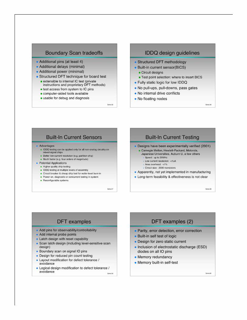
Boundary Scan tradeoffs
Additional pins (at least 4)Additional delays (minimal)Additional power (minimal)Structured DFT technique for board test
extensible to internal IC test (privateinstructions and proprietary DFT methods)test access from system to IC pinscomputer-aided tools availableusable for debug and diagnosis
Soma 56
IDDQ design guidelines
Structured DFT methodologyBuilt-in current sensor(BICS)
Circuit designsTest point selection: where to insert BICS
Fully static logic for low IDDQNo pull-ups, pull-downs, pass gatesNo internal drive conflictsNo floating nodes
Soma 57
Built-In Current Sensors
AdvantagesIDDQ testing can be applied only for all non-analog circuitry onmixed-signal chips
Better low-current resolution (e.g. partition chip)
Much faster (e.g. four orders of magnitude)
Potential ApplicationsHigher quality chip testing
IDDQ testing at multiple levels of assembly
Circuit breaker & cheap chip test for wafer-level burn-in
Power-on, diagnostic or concurrent testing in system
Reconfigurable systems
Soma 58
Built-In Current Testing
Designs have been experimentally verified (2001)Carnegie Mellon, Hewlett-Packard, Motorola,Japanese Universities, Auburn U, a few others
Speed: up to 20MHz
Low current resolution: <1uA
Area overhead: <1%
Circuit size: 2000 transistors
Apparently, not yet implemented in manufacturing
Long-term feasibility & effectiveness is not clear
Soma 59
DFT examples
Add pins for observability/controllabilityAdd internal probe pointsLatch design with reset capabilityScan latch design (including level-sensitive scandesign)Boundary scan on signal IO pinsDesign for reduced pin count testingLayout modification for defect tolerance /avoidanceLogical design modification to defect tolerance /avoidance
Soma 60
DFT examples (2)
Parity, error detection, error correctionBuilt-in self test of logicDesign for zero static currentInclusion of electrostatic discharge (ESD)diodes on all IO pinsMemory redundancy
Memory built-in self-test
Soma 61
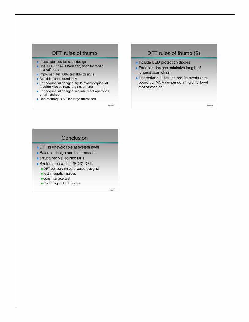
DFT rules of thumb
If possible, use full scan designUse JTAG 1149.1 boundary scan for openmarket partsImplement full IDDq testable designsAvoid logical redundancyFor sequential designs, try to avoid sequentialfeedback loops (e.g. large counters)For sequential designs, include reset operationon all latchesUse memory BIST for large memories
Soma 62
DFT rules of thumb (2)
Include ESD protection diodesFor scan designs, minimize length oflongest scan chainUnderstand all testing requirements (e.g.board vs. MCM) when defining chip-leveltest strategies
Soma 63
Conclusion
DFT is unavoidable at system levelBalance design and test tradeoffsStructured vs. ad-hoc DFTSystems-on-a-chip (SOC) DFT:
DFT per core (in core-based designs)test integration issues
core interface testmixed-signal DFT issues