p i e trg. k and lb po m
TRANSCRIPT

TOWARDS AN ER-DOPED SI NANOCRYSTAL SENSITIZED WAVEGUIDE LASER – THE THIN L INE BETWEEN GAIN AND LOSS
PIETER G. KIK AND ALBERT POLMAN F.O.M. Institute for Atomic and Molecular Physics P.O. Box 41883, 1009 DB Amsterdam, The Netherlands
Important progress is being made in the development of a Si based waveguide laser operating at 1.5 µm. The gain medium responsible for the recent progress is Er-doped Si nanocrystal co-doped SiO2, a composite material that can potentially be fabricated using a VLSI compatible process. The material combines the broad absorption spectrum of Si nanocrystals with the efficient narrow linewidth emission of Er ions. This combination promises to enable the fabrication of a broadband pumped integrated optical amplifier or laser in a Si based materials system. In this paper we systematically discuss the applicability of Si nanocrystals to serve as sensitizers for Er, relating the available data to key sensitizer requirements. 1. Introduction Current Er-doped planar waveguide amplifiers and lasers make use of a pump laser emitting at 0.98 µm that excites Er3+ ions into their second excited state (4I11/2). From this level, the ions quickly relax non-radiatively to the long-lived first excited state (4I13/2) providing the population inversion necessary for gain (see Figure 1(a)). For an Er
545 nm
980 nm
1535 nm
4S3/2 / 2H11/2
4I11/2
4I13/2
4F9/2
4I9/2
4I15/2
650 nm
800 nm
Er3+
1.5
0.98 µµµµm pump
a) b)
Er3+
Si SiO2 (a) (b)
Figure 1(a) Schematic band structure of Er3+ showing excitation at 980 nm followed by non-radiative relaxation to the first excited state and emission at 1.5 µm (b) Schematic band structure of an Er doped Si nanocrystal in SiO2, showing the recombination of a quantum confined electron-hole pair and simultaneous Er excitation.

doped waveguide laser, this means an accurately tuned semiconductor pump laser needs to be integrated with an optical waveguide. This is an expensive approach, since it requires an expensive pump laser and involves a difficult alignment procedure to obtain optimum coupling between pump laser and waveguide. If the pump laser could somehow be eliminated from this scheme, the fabrication of low-cost Si based Er doped optical amplifiers and lasers operating at 1.5 µm would become a real possibility. This is exactly what co-doping with Si nanocrystals promises to do.
It has been observed by several groups1-7 that Er can be excited indirectly in Si nanocrystal doped SiO2. The excitation occurs via optically generated electron-hole pairs inside Si nanocrystals that recombine and transfer energy to the Er ions. Figure 1(b) shows a schematic band diagram of SiO2 containing a Si nanocrystal and Er3+. First a photon is absorbed by the nanocrystal, which causes the generation of an exciton inside the nanocrystal. This exciton can recombine radiatively, emitting a photon with an energy that depends on the nanocrystal size. If an Er ion is present close to the nanocrystal, the exciton can recombine non-radiatively by bringing Er into one of its excited states. Si nanocrystals can be excited in a broad wavelength range (λ< ~1 µm) and have a pump absorption cross-section that is several orders of magnitude higher than the cross-section for direct Er excitation. These two features make codoping with Si nanocrystals a promising route to fabricating integrated waveguide amplifiers and lasers that can be pumped with low-power broadband light sources.
Er excitation via Si nanocrystals must meet several additional requirements to be of use in an optical amplifier. In this article we show measurements that demonstrate (a) the large nanocrystal absorption cross-section σabs > 10-16 cm2, (b) a high energy transfer efficiency η ≥ 55%, (c) the broad absorption band of Si nanocrystals, (d) a high transfer rate R ≥ 106 s-1, (e) a limit to the excitable Er concentration of ~1-2 Er ions per nanocrystal, (f) evidence for free-carrier induced absorption in Si nanocrystal doped optical waveguides, and (g) an unexpected enhancement of the direct optical absorption cross-section of Er in a nanocrystal doped medium. We discuss how all these observations affect the potential use of Er doped Si nanocrystal co-doped SiO2 as an optical gain medium. Finally, calculations will be presented that offer an indication of the net gain that can be expected in this type of waveguide amplifiers. 2. Er sensitizers – requirements A potential sensitizer for Er doped waveguide lasers should satisfy a number of requirements. In this section we list all necessary requirements, and in Section 4 we will discuss how Si nanocrystals perform in these areas. 2.1. ABSORPTION CROSS-SECTION The sensitizer should have a large absorption cross-section to allow for Er population inversion at relatively low pump intensities. It should be noted here that a large cross-section is not always desirable, since a too large cross-section can cause all pump power to be absorbed in a short part of the waveguide, reducing the useful length of the waveguide. For extremely large cross-sections however, a significant fraction of the

pump power can be absorbed when illuminating the waveguide at normal incidence, removing the need for accurate pump coupling. This is an important technological advantage that, as we will show in Section 4.1, can be achieved with Si nanocrystals. 2.2. EXCITATION EFFICIENCY Absorbed energy should be transferred to Er with high quantum efficiency and high power efficiency. In the case of nanocrystals we will show that the quantum efficiency is larger than 55%. The power efficiency is wavelength dependent: when a wavelength of 458 nm is used, the 2.7 eV pump photons generate a 0.8 eV Er excited state, with the excess 1.9 eV transformed into heat. This means that a quantum efficiency of 55% corresponds to a power efficiency of 16%. Consequently, for a high power efficiency it may be advantageous to excite the Si nanocrystals longer wavelengths. Note however that at a longer wavelength the Si absorption cross-section is reduced. 2.3. ABSORPTION LINEWIDTH The pump source is one of the main contributions to the cost of Er doped amplifiers, since it has to perfectly match the narrow Er absorption band at 980 nm. If a sensitizer is used, the pump wavelength needs to be matched to the absorption of the sensitizer. In the case of a sufficiently wide sensitizer absorption band, more cost efficient broadband pump sources such as LEDs can be used for excitation, allowing for a significant cost reduction of the laser or amplifier. 2.4. TRANSFER RATE In any laser or amplifier, the total possible output power is determined by the rate at which the amplifying transition is pumped. In the case of a sensitized Er transition the energy transfer rate from the sensitizer to Er could form an excitation bottleneck. Once the transfer rate has been determined, an estimate of the maximum output power can be made, as will be shown in Section 4.4. 2.5. EXCITABLE FRACTION When using an Er sensitizer, it is essential that all Er ions can be excited. This is especially important for three level systems such as the 1.5 µm transition of Er. In Er3+ the amplifying transition occurs from the first excited state to the ground state, and consequently any fraction of non-excitable Er will efficiently absorb at the signal wavelength. Note that if the amplifying center is a four-level system in which the relevant transition occurs between two excited states, the problem of signal absorption is completely removed.

2.6. INDUCED LOSS Any waveguide loss introduced by the sensitizer will reduce the maximum output power of the sensitized laser or amplifier. Possible loss contributions include increased scattering due to an inhomogeneous sensitizer distribution, changes in the materials processing that introduce waveguide roughness, and introduction of free charges that can lead to free carrier absorption. The last effect is of special relevance to the case of Si nanocrystal sensitization, since the nanocrystal excitation requires the generation of electron-hole pairs, which can in fact absorb at 1.5 µm wavelength. In bulk Si, free carrier absorption cross-sections are as large as 10-17 cm2 around 1.5 µm8. This is more than a factor 1000 higher than a typical Er emission cross-section, meaning that the presence of one exciton for every 1000 Er ions could completely suppress any amplification. It should be noted that free carrier absorption cross-sections in Si nanocrystal doped SiO2 may be reduced compared to those in bulk Si due to quantum size effects, and that the direct Er cross-section at 1.5 µm seems to be enhanced in Si nanocrystal doped SiO2 (see Section 4.6.). 3. Exper imental This paper contains results on two different sample types. The first part deals with thin oxide layers doped with Er and Si nanocrystals by means of ion implantation. For these samples, a 100 nm thick layer of SiO2 was grown on a lightly B-doped Si(100) substrate by means of wet thermal oxidation. This layer was implanted with 35 keV Si to a dose of 6×1016 cm-2. The implantation yields an approximately Gaussian depth distribution of excess Si in the SiO2 fi lm, with a peak concentration of 19 at.% (corresponding to a composition of Si0.46O0.54) at a depth of 45 nm. The samples were subsequently annealed at 1100 ºC for 10 min. in vacuum at a base pressure below 3×10⁻⁷ mbar in order to induce nucleation and growth of Si nanocrystals. This treatment has been shown to produce Si nanocrystals with diameters in the range 2-5 nm.9 Assuming a typical nanocrystal diameter of 3 nm (~103 Si atoms), the nanocrystal peak concentration is estimated to be ~1019 cm-3 at the center of the SiO2 layer. The samples were then implanted with different Er doses in the range 3.6×1013 cm-2 – 5.1×1015 cm-2 at a fixed energy of 125 keV. These implants result in an approximately Gaussian Er depth distribution, with Er peak concentrations ranging from 0.015 at.% to 1.8 at.% at a depth of 61 nm. A non Er-implanted sample was kept as a reference. After the Er implants, all samples (including the non-Er implanted) were annealed for 10 min. in vacuum at 1000 ºC to remove implantation-induced damage. In order to further reduce defect-related luminescence and to saturate dangling bonds on the Si nanocrystal surface, a passivating anneal was performed at 780 ºC for 30 min. in forming gas (H2:N2 at 1:9) at atmospheric pressure.
The second series of experiments involves the fabrication of Er doped nanocrystal sensitized waveguide samples in SiO2. Silicon ions were implanted at 165 keV to a fluence of 1.7×1017 cm-2 into a 5 µm thick layer of SiO2 that was grown by wet thermal oxidation of Si(100). The material was annealed at 1100 ºC for 10 min. in

flowing Ar in order to induce nucleation and growth of Si nanocrystals. The temperature of 1100 ºC was found to yield maximum nanocrystal luminescence. This material was implanted with Er at 700 keV to a fluence of 1.2×1016 cm-2 and annealed at 1000 ºC for 10 min. in flowing Ar to remove implantation induced damage. A sample containing no Er was kept as a reference. These samples were annealed at 800 ºC for 10 min. in forming gas (H2:N2 at 1:9) to optimize the nanocrystal and Er photoluminescence intensity. The excess Si concentration profile peaks at a depth of 240 nm, and has a full width at half maximum (FWHM) of 160 nm. The Si peak concentration is 42 at.%, corresponding to an excess Si concentration of 13 at.%. Assuming an average nanocrystal diameter of 3 nm, the nanocrystal concentration at the peak of the Si profile is estimated to be 1.3×1019 cm-3. The Er concentration profile peaks at a depth of 240 nm, with an Er peak concentration of 1.3 at.% and a FWHM of 130 nm.
A series of 3.5 µm wide ridge waveguides was formed in the implanted and annealed SiO2 film using standard photolithography and Ar beam etching to a depth of 0.5 µm, i.e. well beyond the Si doped region. The excess Si inside the ridges locally raises the index of refraction, providing the index contrast required for transverse and lateral optical mode confinement. To reduce scattering losses, the waveguides were covered with a 1.25 µm thick SiO2 cladding layer using microwave sputtering. The samples were subsequently cut to a length of 8 mm, and the waveguide input and output facets were mechanically polished.
Photoluminescence (PL) measurements on planar samples were taken using the 458 nm line of an Ar laser as excitation source at a peak power of 1 mW in a ~1 mm2 laser spot. The laser beam was modulated on-off at 11 Hz using an acousto-optical modulator. The emitted light was passed through a grating monochromator and detected using standard lock-in techniques. Spectra were measured in the range 600-1150 nm using a AgOCs photomultiplier tube (PMT), and in the range 1100-1700 nm using a liquid-nitrogen cooled Ge detector. All spectra were corrected for the detector response. Photoluminescence decay traces were recorded using a multichannel photon counting system in combination with the PMT and a digitizing oscil loscope in combination with the Ge detector. The system response for the two cases was 150 ns and 160 µs, respectively. Except when noted otherwise, measurements on the planar samples were performed at 15 K using a closed-cycle He cryostat.
Optical transmission measurements on the waveguide samples were performed using a fiber-coupled white l ight source emitting in the 1000-1800 nm range, which was modulated on-off at 270 Hz for lock-in detection. The white light was butt-coupled to the nanocrystal waveguides using a single mode tapered fiber. The transmitted light was collected by imaging the waveguide output facet onto a multimode fiber using a 10× microscope objective. The collected light was led to a grating monochromator and detected using a l iquid nitrogen cooled Ge detector, in combination with standard lock-in techniques. Optical mode images were obtained by coupling 1.49 µm light from an InGaAsP diode laser into the waveguide, and imaging the waveguide output facet on an infrared camera using a 10× microscope objective.
For gain measurements the Si nanocrystal and Er doped waveguides were optically pumped CW using the 458 nm line of an Ar laser. The pump light was projected onto the waveguides from the top using a cylindrical lens. The elongated spot was aligned with the waveguide, and covered the full waveguide length. In this way the

pump power was evenly distributed over the full length of the waveguide. In these measurements the modulated white light source was coupled into the waveguide, and the transmitted signal around 1.5 µm was detected as a function of pump power using lock-in detection.
4. Results and discussion Figure 2 shows a PL spectrum of a SiO2 film doped with Si nanocrystals (labeled "no Er"). The sample shows a broad luminescence band peaking at 790 nm. This luminescence is caused by the radiative recombination of electron-hole pairs (excitons) confined within the Si nanocrystals. Due to quantum confinement10 the exciton luminescence appears at energies above the bandgap energy of bulk Si (1.17 eV at 15 K). The large spectral width of the nanocrystal luminescence in these samples is caused mainly by the broad nanocrystal size distribution (2-5 nm diameter). The luminescence peak at 1.13 µm is caused by phonon-assisted electron-hole pair recombination in the Si substrate. Figure 2 also shows luminescence spectra for samples containing Er at various concentrations. The incorporation of 0.015 at.% Er reduces the nanocrystal luminescence by more than a factor two, and a luminescence peak appears at a wavelength of 1.536 µm. This wavelength corresponds to the radiative transition from the first excited state (4I13/2) to the ground state (4I15/2) of Er3+. Increasing the Er concentration leads to a further reduction of the nanocrystal luminescence intensity, accompanied by an increase of the Er luminescence intensity. The inverse correlation between nanocrystal emission and Er emission is a first indication that Si nanocrystals act as sensitizers for Er. Since the applied excitation wavelength does not overlap with one of the Er absorption lines, the appearance of Er luminescence provides a first indication of sensitized luminescence. In the following section we will look in detail at the behavior of these two luminescence features, and the results will be used to evaluate the potential of Si nanocrystals as Er sensitizers.
Figure 2. Photoluminescence spectra of Si nanocrystal doped SiO2 containing different Er concentrations in the range 0 - 1.8 at.%, measured at 15 K using a pump power of 1 mW at 458 nm.
0.6 0.8 1.0 1.2 1.4 1.60
2
4
6
8
10
Si nanocrystals
Er3+
bulk Si
0.015
0.06
0.170.45
1.80.015
0.06
0.17
0.451.8
no Er
Wavelength (µm)
Inte
nsity
(a.
u.)

4.1. ABSORPTION CROSS-SECTION In order to determine the nanocrystal absorption cross-section, we measured the nanocrystal luminescence 1/e rise time (τr) and decay time (τ) at 5 mW pump power (see time dependent data in Fig. 3(a)). From these two time constants we can deduce the excitation rate R = (1/τr -1/τ), assuming that the nanocrystals effectively behave as a two-level system. At a pump intensity of ~5 mW/mm2 we find for the nanocrystal excitation rate Rnc = σnc × ϕphot = 1040 s-1 with σnc the nanocrystal absorption cross-section and ϕphot the photon flux. Inserting the known photon flux of ~1×1018 cm-2s we find σnc = 9×10-16 cm2. This value is several orders of magnitude larger than direct Er optical absorption cross-sections, which are typically in the 10-21 cm2 range. Note that the value obtained is somewhat larger than other values reported at this excitation wavelength, see e.g. Künzer et al.11 (σabs,458nm ≈ 4×10-16 cm2) and Priolo et al.12 (σabs,488nm ≈ 1×10-16 cm2). This kind of discrepancy may be inherent to the type of measurement: the cross-section depends on the nanocrystal diameter to the ~3rd power, and the obtained value for the effective cross-section depends quadratically on the estimated laser beam diameter.
As was mentioned in the introduction, the large absorption cross-section of Si nanocrystals may allow for unconventional pumping geometries, such as normal-incidence pumping, or side-illumination in which the whole waveguide length is illuminated by a source that is coupled into a slab-waveguide mode. For this type of geometry to be effective, a significant fraction of the pump power should be absorbed within a typical waveguide thickness. To see whether this is possible we can estimate the absorption depth in typical Si nanocrystal doped samples. The absorption depth can be obtained from the absorption coefficient α(cm-1)=σabs×Cnc. If we take a conservative absorption cross-section of 10-16 cm2 and a typical nanocrystal concentration of 1019 cm-3, we obtain an absorption depth d1/e = 1/α = 10 µm. Consequently, pumping at a
0 1 2 30 1 2 3
0.0
0.2
0.4
0.6
0.8
1.0
Time (ms)
PL
Inte
nsity
(a.
u.)
Time (ms)
λem = 750 nm λem = 1536 nm
(a) (b)
Figure 3. Luminescence rise time and decay measurements at 5 mW pump power at 15 K for (a) nanocrystal luminescence at 750 nm, and (b) Er luminescence at 1536 nm

wavelength of 458 nm, 63% of the pump power can be absorbed in a 10 µm thick waveguide. Pumping at shorter wavelengths will further reduce the required waveguide thickness. This shows that pumping either laterally or vertically is a realistic option in this type of material. 4.2. EXCITATION EFFICIENCY In order to determine the Er excitation efficiency, we have also measured the Er luminescence 1/e rise time (τr) and decay time (τ) on the same sample as discussed in Section 4.1 (see Fig. 3(b)) . Under the same pump conditions we find for the Er excitation rate REr = 570 s-1, which is of the same order of magnitude as the previously obtained nanocrystal excitation rate Rnc = 1040 s-1. These numbers give an estimate of the energy transfer efficiency, or the internal quantum efficiency. Assuming each nanocrystal couples to only one Er ion, we conclude that 570/1040=55 % of the generated excitons recombine by transferring energy to the Er ion.13 The obtained 55% is a lower estimate for the excitation efficiency. For example, if we assume each nanocrystal couples to two Er ions, the transfer efficiency would be 2×570/1040 ≈ 100%. The requirement for efficient energy transfer is clearly satisfied. Note that it is difficult to argue that in this sample more than 2 Er ions couple to one nanocrystal, since this would lead to internal quantum efficiencies in excess of 100 %. This apparent concentration limit will be further discussed in Section 4.5. 4.3. ABSORPTION LINEWIDTH Figure 4 shows photoluminescence excitation spectra of the nanocrystal luminescence at 750 nm and the Er luminescence at 1536 nm. At fixed pump power, the nanocrystal luminescence intensity and the Er luminescence intensity are seen to increase by a factor of two when the excitation wavelength is decreased from 514 nm to 458 nm. The
Figure 4. Excitation spectrum of the nanocrystal luminescence at 750 nm and the Er luminescence at 1536 nm. The dotted line is a guide to the eye. The vertical bands indicate the position of direct Er optical absorption lines.
460 480 500 5200
10
20
30
40
nanocrystal luminescence erbium luminescence
pump wavelength (nm)
PL
Inte
nsity
(a.
u.)

absence of absorption resonances in the Er excitation spectrum indicates that the Er is not excited directly by absorption of pump photons, but indirectly via an energy transfer process from Si nanocrystals, as was already suggested above. The observed wavelength dependence of the luminescence intensity is attributed to the increasing nanocrystal optical absorption cross-section for increasing photon energy, leading to a higher exciton generation rate. These results give direct evidence that Er in this material can be excited in a broad wavelength range, allowing for broadband pumping of amplifiers and lasers based on this materials system. 4.4. TRANSFER RATE Figure 5 shows nanocrystal luminescence decay traces taken at 750 nm and T=15 K for samples containing different Er concentrations. In a sample containing no Er, the nanocrystal luminescence shows a 1/e lifetime of 2.0 ms. The decay is described by a stretched exponential decay of the form I(t)=exp(-(t/τ)β) with τ=2.0 ms and β=0.65 (solid line). The same curve has been overlaid on all data in order to facilitate comparison between the different traces. Incorporation of Er leads to a significant reduction of the nanocrystal luminescence intensity at 750 nm, as was already observed in Fig. 2. The decay time however varies only slightly from sample to sample, and no trend is observed with increasing Er concentration. The sample containing the highest Er concentration shows a small initial fast decay, which is attributed to luminescence from defects in the SiO2 matrix. These lifetime measurements confirm the strong-coupling model,6 which states that the Er induced nanocrystal PL intensity decrease in Fig. 2 is effectively due to a reduction in the number of luminescent nanocrystals. All remaining nanocrystal luminescence originates from nanocrystals that are not coupled to Er, which show their intrinsic decay characteristics. This model also explains the initially surprising observation that the Er luminescence intensity is virtually
Figure 5. Photoluminescence decay traces of the nanocrystal luminescence at 750 nm for different Er concentrations in the range 0 - 1.8 at.%, measured at 15 K using 1 mW pump power at 458 nm. The pump is
switched off at t=0. The drawn lines represent stretched exponential decay with τ=2.0 ms and β=0.65.
0 1 2 3 4 5 6 7
0.1
1
10
1.8 at.%
0.17 at.%
0.015 at.%
no Er
Inte
nsity
(a.
u.)
Time (ms)

temperature independent, whereas the nanocrystal luminescence intensity varies by as much as a factor 4 in the temperature range 20 K - 300 K. This behavior is now understood: in nanocrystals that do not couple to Er, temperature dependent radiative and non-radiative exciton recombination rates affect the luminescence efficiency, while in nanocrystals that couple to Er, the non-radiative transfer to Er is the dominant recombination process, occurring at a (high) fixed efficiency over the full temperature range. These observations also allow us to obtain an upper limit to the energy transfer rate constant, since the energy transfer has to occur at a significantly higher rate than the spontaneous exciton recombination in order to be the dominant recombination mechanism. The fastest observed nanocrystal decay time in these samples is 21 µs, and consequently the energy transfer has to occur faster than ~1 µs. Given the obtained value for the energy transfer rate of (1 µs)-1 = 106 s-1, we can determine the maximum output power of an Er doped Si nanocrystal sensitized waveguide amplifier. Assuming a nanocrystal concentration of 1019 cm-3 and 2 excitable Er ions per nanocrystal in a 10 µm×10 µm=10-6 cm2 waveguide, we find a maximum output power of 2×1019 cm-3 × 10⁻⁶ cm2 × 106 s-1 × 0.8 eV = 2.6 W/cm. This shows that the transfer rate is sufficiently fast to allow for the amplification of high power signals over short waveguide lengths. 4.5. EXCITABLE FRACTION Figure 6 shows the effect of pump power on the Er and nanocrystal luminescence intensity for samples containing 0.015 at.% Er and 1.8 at.% Er respectively. At pump powers below 20 µW the Er luminescence in both samples depends l inearly on pump power, and the Er luminescence intensities from the two samples differ by a factor of ~2. Increasing the pump power produces a sub-linear increase of the Er luminescence in both samples, suggesting that a significant fraction of the excitable Er is brought into
Figure 6. Photoluminescence intensity of the Er luminescence intensity as a function of pump power for samples containing 0.015 at.% and 1.8 at.% Er, measured at 15 K using 458 nm pump light in a ~1 mm2 spot.
104
103
102
101
100
10210110010-3
0.015 at.%
1.8 at.%
Er
Er
Pump power (mW)
PL
Inte
nsity
(a.
u.)
10-110-2

the first excited state, or that non-radiative processes come into play. At a pump power of 50 mW the Er luminescence intensity appears to level off. In this pump power regime the exciton generation rate is no longer the limiting factor for the Er luminescence intensity. Nevertheless, the Er luminescence intensities for the two samples at 50 mW pump power differ by only a factor 5, even though the total amount of Er in the samples differs by more than a factor 100.
The above shows that the concentration of excitable Er in the high concentration (1.8 at.%) sample is at most 5 times higher than in the low concentration (0.015 at.%) sample. This means that the concentration of excitable Er in these samples is less than 5×0.015 = 0.1 at.%. The existence of such a concentration limit is also observed in the Er excitation rate, as will be shown below.
When the number of Er ions coupled to a nanocrystal is increased, the Er excitation rate per ion can be expected to decrease, since several Er ions now compete for the same excitons. In order to determine the concentration dependent Er excitation rate, we performed rise time and decay time measurements of the Er luminescence at 1.536 µm. At the applied pump power of 1 mW all samples show approximately exponential time dependencies. Figure 7(a) shows the measured rates Wrise=1/τrise (�) and Wdecay=1/τdecay (�) obtained by exponential fitting of the data.
The Er decay rate increases from 500 s-1 to 700 s-1 as the Er peak concentration is increased from 0.015 at.% to 1.8 at.%. This increase is attributed to a concentration quenching effect which is known to occur when rare earth ions are spaced closely enough to allow for energy exchange between neighboring ions. As a result, excitation energy can migrate14 to neighboring ions, which may in turn be coupled non-radiatively to quenching sites, e.g. defects or OH groups present in the matrix. In a simple
Figure 7.(a) Rise times (�) and decay times (�) of the 1.536 µm Er luminescence, measured at 15 K using a pump power of 1 mW at 458 nm, and (b) the Er excitation rate derived from these data (�). The drawn lines serve as a guide to the eye. The dotted line indicates a 1/CEr dependence.
0
250
500
750
1000
1250
15000.1 1 10
0.01 0.1 10
200
400
600
Er ions per nanocrystal
10
1
2
5 Tim
e co
nst
ant
(m
s)
1/τdown
1/τup
Rat
e (
s-1)
10
1
2
5 Tim
e c
ons
tan
t (m
s)
Rexc
Er peak concentration (at.%)
Ra
te (
s-1)
(a)
(b)

concentration quenching model, the Er decay rate increases linearly with Er concentration, which is indeed observed in Fig. 7(a). By measuring the slope of the decay rate data in Fig. 7(a), we estimate15 that the concentration of quenching sites in the Er implanted Si nanocrystal doped SiO2 film is as low as 1018 cm-3.
Data for the Er excitation rate Rexc calculated from τrise and τdecay are shown in Fig. 7(b) (�). At an Er concentration of 0.015 at.%, the Er excitation rate is 600 s-1. Increasing the Er concentration to 0.17 at.% reduces the excitation rate by a factor 2. A further increase of the Er concentration has no effect on the excitation rate, even though at these concentrations several Er ions might couple to the same nanocrystal, which would reduce the excitation rate per Er ion. The fact that such a reduction is not observed, shows that there is an upper limit to the number of Er ions that can be excited by a single nanocrystal. From the data in Fig. 7(b) it is clear that this limit is reached at an Er concentration < 0.17 at.% Er, which is consistent with the maximum value of 0.1 at.% Er found in the preceding paragraph. The existence of an upper limit to the amount of excitable Er could indicate that there is a limit to the amount of optically active Er that can be incorporated in this material. This may for example be caused by Er clustering or ErSi2 formation, which would prevent the Er from being in the 3+ valence state. However, measurements on Er and Si nanocrystal doped waveguides show a strong Er3+ related absorption,16 suggesting that a large fraction of the Er is in the optically active state. Alternatively, the observed concentration limit could be an intrinsic property of the excitation process. The amount of excitable Er will be low when the effective Er excitation efficiency is reduced by the presence of excited Er. Such a situation arises when the formation of an exciton near an excited Er ion leads to
Figure 8. Schematic band diagram of Er and Si nanocrystal doped SiO2 showing the process of (a) Auger de-excitation, and (b) pair-induced quenching. These processes can account for the observed Er concentration limit in Si nanocrystal doped SiO2. Note that the Er energy levels represent collective states of the Er3+ 4f electrons, which are in fact well below the SiO2 valence band edge.
SiO2Si
Er3+
(a)
SiO2Si
(b)
Er3+ Er3+

a) Auger de-excitation, in which an excited Er ion transfers energy to an exciton present in the nanocrystal (Fig. 8(a)). This process has been shown to occur in Er doped bulk Si.17 After such Auger de-excitation the exciton can relax and subsequently excite an Er ion, effectively bringing the system back to the situation before the exciton was formed.
b) pair-induced quenching. At a sufficiently high Er concentration, two excited Er ions can interact yielding one Er ion in the 4I9/2 state, which rapidly decays to the first excited state, and one Er ion in the ground state (Fig. 8(b)). This co-operative upconversion effect usually produces a shortening of the Er decay rate at high pump powers, which has not been observed. However, if the Er-Er coupling is sufficiently strong, no effect on the li fetime is seen. This special case is called pair-induced quenching.
Evidence for upconversion has been found in Er doped Si nanocrystal sensitized optical waveguides when pumped at 1.49 µm (see Fig. 9), and in planar samples containing Er and Si nanocrystals pumped at visible wavelengths.18 The latter observation suggests that a high concentration of excited Er can in fact be obtained in this type of material. 4.6. INDUCED LOSSES Figure 10 shows iso-intensity contours of two optical mode images taken using 1.49 µm light from an InGaAsP laser guided through the waveguide. The emission from the output facet was projected onto an infrared camera using a microscope objective. At this wavelength both waveguides only support the fundamental mode. For the smallest
50 µµµµm
Figure 9. Top view of an array of Er doped Si nanocrystal based channel waveguides, one of which is pumped with ~10 mW at a wavelength of 1.49 µm using a tapered optical fiber. The bright (green) emission from the waveguide is caused by radiative relaxation from the 4S3/2 and 2H11/2 levels that are populated in a two-step co-operative upconversion process.

waveguide (width 1 µm) the mode is observed to be approximately circular, with a full width at half-maximum (FWHM) of 2.8 µm in the x-direction, and 3.0 µm in the y-direction. For the 3.5 µm wide waveguide, the mode is observed to be slightly elliptical, with a full width at half-maximum (FWHM) of 4.5 µm in the x-direction, and 3.5 µm in the y-direction. From these modes and the known Er depth profile, an effective mode overlap Γ with the Er doped region can be obtained. For the 3.5 µm waveguide this overlap is found to be 1%.
Figure 11 shows normalized transmission spectra of Si nanocrystal waveguides containing no Er (dashed line) and 1.3 at.% Er (solid line), measured using a fiber coupled white light source butt-coupled to the nanocrystal waveguide using a single-mode tapered fiber. In the Er doped sample a clear dip is observed around 1.53 µm, due
Figure 10. Optical mode images at a wavelength of 1.49 mm taken at the output facet of two Er doped Si nanocrystal based ridge waveguides with widths of (a) 1 µm and (b) 3.5 µm respectively. The contour l ines indicate constant intensities. A sketch of the waveguide structure is included
Si (n=3.5)
SiO2
air (n=1.0)
SiO2 (n=1.44)
-4 -2 0 2 4
-6
-4
-2
0
2
x position (µm)
y p
ositi
on
(µm
)
Si (n=3.5)
SiO2
air (n=1.0)
SiO2 (n=1.44)
Si (n=3.5)
0.9 0.7
0.5 0.3
0.1
-4 -2 0 2 4
-6
-4
-2
0
2
x position (µm)
y p
osi
tion
(µm
)
0.7 0.5
0.3 0.1
Si (n=3.5)
0.9
Figure 11. Transmitted signal in a 0.8 cm long Si nanocrystal based waveguides containing no Er (dotted line) and 1.3 at.% Er (solid line).
1.45 1.50 1.55 1.60 1.65 1.700
1
2
3
Wavelenght (µm)
Tra
nsm
issi
on (
a.u.
)

to the 4I15/2 → 4I13/2 absorption transition of Er3+. The peak absorption at 1.532 µm is found to be 2.7 dB/cm. From this value and the measured values for Γ and NEr we obtain an absorption cross-section σEr(1.532 µm) = 8×10-20 cm2. This value is more than a factor ten larger than values found in Er doped Si (2×10-20 cm-2)19 and SiO2 (~4×10-21 cm2). Evidence for such an unusually high cross-section has recently also been found by Han et al.7 and Dal Negro et al.20 The large cross-section may be due to the strong asymmetry of the local dielectric environment of the excitable Er3+ ions (note that in a perfectly symmetrical geometry the 4I13/2→4 I15/2 transition is parity-forbidden). This may also explain the relatively short luminescence lifetimes typically observed in this type of material. The high absorption cross-section also translates into a high emission cross-section,21,22 which implies that high gain could be achieved in this material over a short length.
Figure 12 shows the transmitted signal at 1.535 µm as a function of applied pump power at 458 nm. The same pump power dependence of the transmitted signal was observed at all wavelengths in the range 1.4-1.7 µm. Apparently, instead of producing gain, optical pumping at 458 nm induces an absorption in the waveguide material. Figure 13 shows the time dependent transmission at 1.535 µm after pump switch-on and switch-off. Note that after pump switch-off, the signal transmission returns to approximately its original value over a period of several minutes.
The observed transmission change could be due to free carrier absorption, a well-known effect in bulk silicon, in which free carriers absorb sub-bandgap radiation due to intra-band transitions.23 The free carriers causing the absorption feature are not present in the form of quantum confined electron-hole pairs, since these recombine at a rate of ~105 s-1 at room temperature.6,24 However, if the charge carriers are physically separated, their lifetime can increase by orders of magnitude.25 Such separation could occur when during pumping one of the carriers in an electron-hole pair is ejected into a
Figure 12. Transmitted signal at 1.535 µm as a function of the applied continuous-wave 458 nm pump power as obtained from transmission measurements. The transmission at zero pump power includes the waveguide loss and Er ground state absorption. A sketch of the measurement configuration is included.
0.00 0.05 0.10 0.15 0.200
100
200
300
Pump power (W)
Tra
nsm
isse
d si
gnal
(a.
u.)
1.5 µµµµm
458 nm

deep trap state near the nanocrystal surface, or when one of the carriers tunnels into a neighboring nanocrystal. The latter process is indicated schematically in Fig. 13.
The data in Fig. 12 can be used to estimate the pump-induced free carrier concentration. The maximum transmission reduction is approximately 1.7 dB, which corresponds to α=-0.5 cm-1 given the waveguide length of 8 mm. Taking α(cm-1) =
σfc×Ncarr×Γ with σfc a typical free carrier absorption cross-section in bulk Si at 1.5 µm8 of 7×10-18 cm2, Ncarr the concentration of pump-induced free carriers in the waveguide, and Γ=0.01 the previously determined mode overlap with the Si nanocrystal doped region, we find Ncarr=0.7×1019 cm-3, close to one carrier per nanocrystal. Note that this kind of pump induced absorption has not been observed in nanocrystal doped waveguides with lower excess Si concentrations,7 possibly due to larger spacing between nanocrystals.
If the observed transmission reduction is indeed caused by single charges in separate nanocrystals, the recombination rate of these charges can be expected to decrease rapidly as the concentration of free charges decreases. This type of ‘bimolecular recombination’ can be described by the following rate equation:
2carr
carr CNRdt
dN −= (1)
with Ncarr the concentration of isolated carriers, R the generation rate of isolated carriers, and C(cm3s-1) a proportionality constant relating the recombination rate to the carrier concentration. If we assume a linear relation between the carrier generation rate and the pump power, the steady state solution gives Ncarr ∝ P1/2. The solid l ine in Fig. 12 corresponds to a transmission T=exp(-α(P)L) with L=0.8 cm the waveguide length and
Figure 13. Time dependence of the 1.5 µm transmission of an Er and Si nanocrystal doped optical waveguide excited with a 458 nm pump laser directly after pump switch-on (left panel) and pump switch-off (right panel).
0 2 4 6 8 100
1
2
3
0 2 4 6 8 10
Tra
nsm
itted
1.5
µm
sig
nal (
a.u.
)
time (m)
time (m)

α(cm-1)=σfc×Ncarr(P)×Γ, where we have taken Ncarr∝P1/2. It is clear that the simple rate equation model can produce a good fit of the observed behavior.
Equation (1) can also be used to describe the time dependence of the pump induced absorption. In Fig. 14 we have plotted -ln(T) over time after pump switch-off. Using the measured mode overlap, the bulk Si free-carrier absorption cross-section, and the known waveguide length, each value of -ln(T) can be converted to Ncarr, as indicated on the right axis. We should be able to describe this curve with equation (1) setting the pump rate to zero. In this pump-off condition the solution is of the form Ncarr(t)=A/t, with A a scaling factor indicating the initial carrier concentration and the proportionality constant relating the recombination rate to the carrier concentration. This dependency is indicated in Fig. 14 by the drawn line. Except for an initial fast drop in the concentration, the curve describes the time dependent carrier concentration quite well. Despite the shortcomings of the model (no nanocrystal size dependence, no absorption by quantum confined excitons) the proposed process of tunneling-limited carrier recombination can indeed describe the main features of the observed pump-induced absorption. 5. The thin line between gain and loss In this Section we discuss a simple gain model that includes the main processes determining the gain of an Er doped Si nanocrystal sensitized waveguide amplifier. The model includes stimulated emission by excited Er, absorption by Er in the ground state, absorption by free carriers present in nanocrystals not coupled to Er, and absorption by carriers present in Si nanocrystals that are coupled to Er. We have made the following assumptions: 1) the Er ions, the Si nanocrystals coupled to Er, and the Si nanocrystals
Figure 14. Time dependence of the calculated f ree-carrier concentration as discussed in section 4.6. The solid l ine is the solution of a rate equation model describing tunneling assisted bimolecular recombination of separated charges.
12 14 16 18 20 220.0
0.1
0.2
0.3
0.4
0.5
- ln
(tra
nsm
issi
on)
time (min.)
0
1
2
3
4
5
6
7
Fre
e ca
rrie
r co
ncen
trat
ion
(101
8 cm
-3)
-
+ -
+
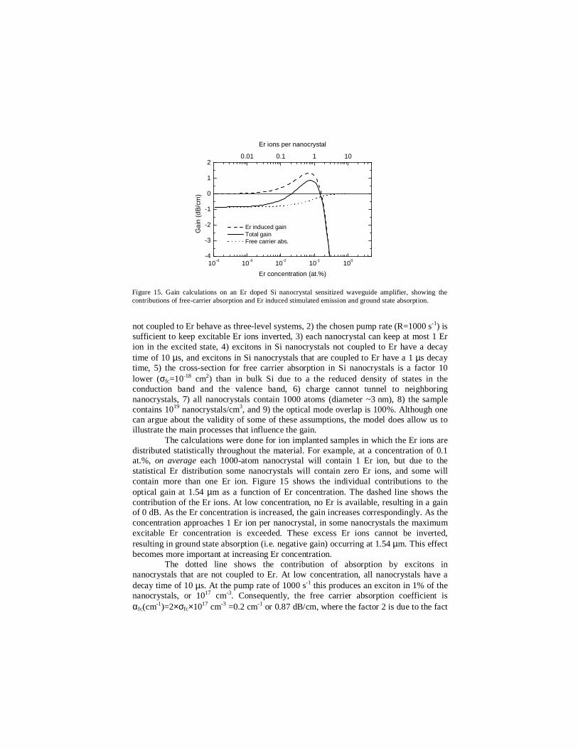
not coupled to Er behave as three-level systems, 2) the chosen pump rate (R=1000 s-1) is sufficient to keep excitable Er ions inverted, 3) each nanocrystal can keep at most 1 Er ion in the excited state, 4) excitons in Si nanocrystals not coupled to Er have a decay time of 10 µs, and excitons in Si nanocrystals that are coupled to Er have a 1 µs decay time, 5) the cross-section for free carrier absorption in Si nanocrystals is a factor 10 lower (σfc=10-18 cm2) than in bulk Si due to a the reduced density of states in the conduction band and the valence band, 6) charge cannot tunnel to neighboring nanocrystals, 7) all nanocrystals contain 1000 atoms (diameter ~3 nm), 8) the sample contains 1019 nanocrystals/cm3, and 9) the optical mode overlap is 100%. Although one can argue about the validity of some of these assumptions, the model does allow us to illustrate the main processes that influence the gain.
The calculations were done for ion implanted samples in which the Er ions are distributed statistically throughout the material. For example, at a concentration of 0.1 at.%, on average each 1000-atom nanocrystal will contain 1 Er ion, but due to the statistical Er distribution some nanocrystals will contain zero Er ions, and some will contain more than one Er ion. Figure 15 shows the individual contributions to the optical gain at 1.54 µm as a function of Er concentration. The dashed l ine shows the contribution of the Er ions. At low concentration, no Er is available, resulting in a gain of 0 dB. As the Er concentration is increased, the gain increases correspondingly. As the concentration approaches 1 Er ion per nanocrystal, in some nanocrystals the maximum excitable Er concentration is exceeded. These excess Er ions cannot be inverted, resulting in ground state absorption (i.e. negative gain) occurring at 1.54 µm. This effect becomes more important at increasing Er concentration.
The dotted line shows the contribution of absorption by excitons in nanocrystals that are not coupled to Er. At low concentration, all nanocrystals have a decay time of 10 µs. At the pump rate of 1000 s-1 this produces an exciton in 1% of the nanocrystals, or 1017 cm-3. Consequently, the free carrier absorption coefficient is αfc(cm-1)=2×σfc×1017 cm-3 =0.2 cm-1 or 0.87 dB/cm, where the factor 2 is due to the fact
Figure 15. Gain calculations on an Er doped Si nanocrystal sensitized waveguide amplifier, showing the contributions of free-carrier absorption and Er induced stimulated emission and ground state absorption.
10-4 10-3 10-2 10-1 100-4
-3
-2
-1
0
1
2
Er induced gain Total gain Free carrier abs.
Er concentration (at.%)
Ga
in (
dB
/cm
)
0.01 0.1 1 10
Er ions per nanocrystal

that an exciton consists of two free charges. As the Er concentration is increased, the chance for a nanocrystal to be coupled to Er increases, which reduces the exciton lifetime to 1 µs, resulting in reduced free carrier absorption. Since the lifetime of coupled nanocrystals is a factor ten less than that of non-coupled nanocrystals, the maximum absorption due to excitons generated in coupled nanocrystals at this pump rate is approximately 0.1×0.87 dB/cm ≈ 0.1 dB/cm. This contribution is negligible in Fig. 15 but could become significant at higher pump powers. The solid line shows the sum of the two gain contributions, illustrating that net gain can be achieved only in a narrow Er concentration range.
The gain calculations in Fig. 15 can be considered a worst case scenario in several ways. For one thing, there is as yet no clear consensus on the maximum number of excitable Er ions per nanocrystal, the estimates ranging from 1 to 100. A higher concentration of excitable Er will dramatically increase the maximum attainable gain. Additionally, the free-carrier absorption observed at low Er concentration is caused by nanocrystals that are not coupled to Er. It seems feasible that a fabrication process can be developed that prevents the formation of uncoupled nanocrystals. One point of concern may be the signal power. The gain calculations were done in a relatively low pump power regime. When high intensity signals are amplified, higher pump rates will be necessary. It seems likely that given the finite lifetime of excitons in nanocrystals coupled to Er, a significant free-carrier concentration may be built up at high pump power. This could put an upper limit on the signal strength that can be amplified.
6. Conclusions We have shown that Er excitation via Si nanocrystals can satisfy all requirements to be used in broadband pumped integrated optical waveguide amplifiers and lasers operating at 1.5 µm. In particular, it was shown that (a) the Si nanocrystal absorption cross-section at visible wavelengths is several orders of magnitude larger than direct Er optical absorption cross-sections, allowing for low pump-thresholds and unconventional pumping geometries, (b) the energy transfer quantum efficiency is larger than 55%, (c) energy transfer to Er occurs under visible excitation in a broad wavelength band, allowing for broadband pumping using cost-effective light sources such as LEDs, (d) the energy transfer rate is larger than 106 s-1, in principle allowing for the generation of several hundreds of milliwatts 1.5 µm power in a 1 cm long waveguide, (e) concentrations of optically active Er in excess of 1019 cm-3 may be excited via nanocrystals, (f) optical pumping of Er doped nanocrystal sensitized waveguides can introduce a broad absorption in the infrared, possibly due to free-carrier absorption, and (g) the direct optical absorption cross-section of Er in a nanocrystal doped medium is enhanced by a factor ~10 compared to the absorption cross-section in typical SiO2 based hosts. Gain calculations taking into account all these observations suggest that net gain at 1.5 µm in excess of 1 dB/cm can be achieved in Er doped Si nanocrystal sensitized optical waveguide amplifiers.

7. References 1 S. Lombardo, S. U. Campisano, G. N. van den Hoven, A. Cacciato, and A. Polman, Appl. Phys. Lett. 63,
1942 (1993) 2 A. J. Kenyon, P. F. Trwoga, M. Federighi, and C. W. Pitt, J. Phys. Cond. Matter 6, L319 (1994) 3 M. Fujii, M. Yoshida, Y. Kanzawa, S. Hayashi, and K. Yamamoto, Appl. Phys. Lett. 71, 1198 (1997) 4 J. St. John, J. L. Coffer, Y. Chen, and R. F. Pinizzotto, J. Am. Chem. Soc. 121, 1888 (1998) 5 G. Franzò, V. Vinciguerra, and F. Priolo, Appl. Phys. A. 69, 3 (1999) 6 P. G. Kik, M. L. Brongersma, and A. Polman, Appl. Phys. Lett. 76, April 24 (2000) 7 H. S. Han, S.Y. Seo, and J. H. Shin, Appl. Phys. Lett. 79, 4568 (2001) 8 M. A. Green, Silicon solar cells (University of New South Wales, Sydney, 1995), p. 48 9 M.L. Brongersma, A. Polman, K.S. Min, E. Boer, T. Tambo, and H.A. Atwater, Appl. Phys. Lett. 72, 2577
(1998) 10 C. Delerue, G. Allan, and M. Lannoo, Phys. Rev. B 48, 11024 (1993) 11 D. Kovalev, J. Diener, H. Heckler, G. Polisski, N. Künzner, and F. Koch, Phys. Rev. B 61, 4485 (2000) 12 F. Priolo, G. Franzò, F. Iacona, D. Pacifici and V. Vinciguerra, Mat. Sc. Eng. B 81, 9 (2001) 13 We assume that the nanocrystal absorption cross-section and spontaneous lifetime are not affected by the
presence of Er 14 W. J. Miniscalco, J. Lightwave Technol. 9, 234 (1991) 15 F. Auzel, in Radiationless processes, B. DiBartolo, Ed. (Plenum Press, New York, 1980) 16 P. G. Kik and A. Polman, J. Appl. Phys. 91, 534 (2002) 17 F. Priolo, G. Franzò, S. Coffa, and A. Carnera, Phys. Rev. B 57, 4443 (1998) 18 D. Pacifici et al., Proc. NATO Workshop on Optical Amplification and Stimulation in Silicon (2002) 19 N. Hamelin, P.G. Kik, J.F. Suyver, K. Kikoin, A. Polman, A. Schönecker, and F.W. Saris, J. Appl. Phys. 88,
5381 (2000). 20 L. Dal Negro, private communication 21 D.E. McCumber, Phys. Rev. 136, A 954 (1964). 22 W.J. Miniscalco, and R.S. Quimby, Opt. Lett. 16, 258 (1991). 23 W. Spitzer and H.Y. Fa, Phys. Rev. 108, 268 (1957). 24 M. Hybertsen, Phys. Rev. Lett. 72, 1514 (1994). 25 C. Svensson, in The Si-SiO2 system, edited by P. Balk (Elsevier, 1988)