p8p parallel phase change memory (pcm) data sheet sheets/micron technology inc... · in pcm, the...
TRANSCRIPT

128Mb: P8P Parallel PCMFeatures
P8P Parallel Phase ChangeMemory (PCM)
Features• High-performance READ
– 115ns initial READ access – 135ns initial READ access– 25ns, 8-word asynchronous-page READ
• Architecture– Asymmetrically blocked architecture– Four 32KB parameter blocks with top or bottom
configuration– 128KB main blocks– Serial peripheral interface (SPI) to enable lower
pin count on-board programming• Phase change memory (PCM)
– Chalcogenide phase change storage element– Bit-alterable WRITE operation
• Voltage and power– VCC (core) voltage: 2.7–3.6V – VCCQ (I/O) voltage: 1.7–3.6V – Standby current: 80µA (TYP)
• Quality and reliability– More than 1,000,000 WRITE cycles– 90nm PCM technology
• Temperature– Commercial: 0°C to +70°C (115ns initial READ
access)– Industrial: –40°C to +85°C (135ns initial READ
access)• Simplified software management
– No block erase or cleanup required– Bit twiddle in either direction (1:0, 0:1)– 35µs (TYP) PROGRAM SUSPEND– 35µs (TYP) ERASE SUSPEND– Flash data integrator optimized– Scalable command set and extended command set
compatible– Common Flash interface capable
• Density and packaging– 128Mb density – 56-lead TSOP package– 64-ball easy BGA package
Products and specifications discussed herein are
PDF: 09005aef8447d46d/Source: 09005aef845b5c96parallel_pcm_1.fm - Rev. K 7/12 EN 1
• Security– One-time programmable registers
64 unique factory device identifier bits2112 user-programmable OTP bits
– Selectable OTP space in main array– Three adjacent main blocks available for boot code
or other secure information– Absolute WRITE protection: VPP = VSS– Power transition ERASE/PROGRAM lockout– Individual zero-latency block locking– Individual block lock-down
subject to change by Micron without notice.
Micron Technology, Inc., reserves the right to change products or specifications without notice.©2005 Micron Technology, Inc. All rights reserved.

128Mb: P8P Parallel PCMTable of Contents
Table of ContentsFeatures . . . . . . . . . . . . . . . . . . . . . . . . . . . . . . . . . . . . . . . . . . . . . . . . . . . . . . . . . . . . . . . . . . . . . . . . . . . . . . . . . . . . . . . . . . . . . .1Functional Description . . . . . . . . . . . . . . . . . . . . . . . . . . . . . . . . . . . . . . . . . . . . . . . . . . . . . . . . . . . . . . . . . . . . . . . . . . . . . . . .7Product Features . . . . . . . . . . . . . . . . . . . . . . . . . . . . . . . . . . . . . . . . . . . . . . . . . . . . . . . . . . . . . . . . . . . . . . . . . . . . . . . . . . . . . .7Memory Maps . . . . . . . . . . . . . . . . . . . . . . . . . . . . . . . . . . . . . . . . . . . . . . . . . . . . . . . . . . . . . . . . . . . . . . . . . . . . . . . . . . . . . . . .8Package Dimensions . . . . . . . . . . . . . . . . . . . . . . . . . . . . . . . . . . . . . . . . . . . . . . . . . . . . . . . . . . . . . . . . . . . . . . . . . . . . . . . . .11
TSOP Mechanical Specifications . . . . . . . . . . . . . . . . . . . . . . . . . . . . . . . . . . . . . . . . . . . . . . . . . . . . . . . . . . . . . . . . . . . .1164-Ball Easy BGA Package . . . . . . . . . . . . . . . . . . . . . . . . . . . . . . . . . . . . . . . . . . . . . . . . . . . . . . . . . . . . . . . . . . . . . . . . . .13
Pinouts and Ballouts. . . . . . . . . . . . . . . . . . . . . . . . . . . . . . . . . . . . . . . . . . . . . . . . . . . . . . . . . . . . . . . . . . . . . . . . . . . . . . . . . .14Signal Names and Descriptions . . . . . . . . . . . . . . . . . . . . . . . . . . . . . . . . . . . . . . . . . . . . . . . . . . . . . . . . . . . . . . . . . . . . . . . .16Bus Operations . . . . . . . . . . . . . . . . . . . . . . . . . . . . . . . . . . . . . . . . . . . . . . . . . . . . . . . . . . . . . . . . . . . . . . . . . . . . . . . . . . . . . .17
READ Operations . . . . . . . . . . . . . . . . . . . . . . . . . . . . . . . . . . . . . . . . . . . . . . . . . . . . . . . . . . . . . . . . . . . . . . . . . . . . . . . . . .17WRITE Operations . . . . . . . . . . . . . . . . . . . . . . . . . . . . . . . . . . . . . . . . . . . . . . . . . . . . . . . . . . . . . . . . . . . . . . . . . . . . . . . . .17OUTPUT DISABLE Operations . . . . . . . . . . . . . . . . . . . . . . . . . . . . . . . . . . . . . . . . . . . . . . . . . . . . . . . . . . . . . . . . . . . . . .17STANDBY Operations . . . . . . . . . . . . . . . . . . . . . . . . . . . . . . . . . . . . . . . . . . . . . . . . . . . . . . . . . . . . . . . . . . . . . . . . . . . . . .17RESET Operations . . . . . . . . . . . . . . . . . . . . . . . . . . . . . . . . . . . . . . . . . . . . . . . . . . . . . . . . . . . . . . . . . . . . . . . . . . . . . . . . .18
Command Set . . . . . . . . . . . . . . . . . . . . . . . . . . . . . . . . . . . . . . . . . . . . . . . . . . . . . . . . . . . . . . . . . . . . . . . . . . . . . . . . . . . . . . .18Device Command Codes . . . . . . . . . . . . . . . . . . . . . . . . . . . . . . . . . . . . . . . . . . . . . . . . . . . . . . . . . . . . . . . . . . . . . . . . . . .18
Device Command Bus Cycles. . . . . . . . . . . . . . . . . . . . . . . . . . . . . . . . . . . . . . . . . . . . . . . . . . . . . . . . . . . . . . . . . . . . . . . . . .20READ Operations . . . . . . . . . . . . . . . . . . . . . . . . . . . . . . . . . . . . . . . . . . . . . . . . . . . . . . . . . . . . . . . . . . . . . . . . . . . . . . . . . . . .21
READ ARRAY . . . . . . . . . . . . . . . . . . . . . . . . . . . . . . . . . . . . . . . . . . . . . . . . . . . . . . . . . . . . . . . . . . . . . . . . . . . . . . . . . . . . . .21READ IDENTIFIER . . . . . . . . . . . . . . . . . . . . . . . . . . . . . . . . . . . . . . . . . . . . . . . . . . . . . . . . . . . . . . . . . . . . . . . . . . . . . . . . .22READ QUERY . . . . . . . . . . . . . . . . . . . . . . . . . . . . . . . . . . . . . . . . . . . . . . . . . . . . . . . . . . . . . . . . . . . . . . . . . . . . . . . . . . . . .22
PROGRAM Operations . . . . . . . . . . . . . . . . . . . . . . . . . . . . . . . . . . . . . . . . . . . . . . . . . . . . . . . . . . . . . . . . . . . . . . . . . . . . . . . .23WORD PROGRAM . . . . . . . . . . . . . . . . . . . . . . . . . . . . . . . . . . . . . . . . . . . . . . . . . . . . . . . . . . . . . . . . . . . . . . . . . . . . . . . . .23BIT-ALTERABLE WORD WRITE . . . . . . . . . . . . . . . . . . . . . . . . . . . . . . . . . . . . . . . . . . . . . . . . . . . . . . . . . . . . . . . . . . . . .24BUFFERED PROGRAM . . . . . . . . . . . . . . . . . . . . . . . . . . . . . . . . . . . . . . . . . . . . . . . . . . . . . . . . . . . . . . . . . . . . . . . . . . . . .24BIT-ALTERABLE BUFFER WRITE. . . . . . . . . . . . . . . . . . . . . . . . . . . . . . . . . . . . . . . . . . . . . . . . . . . . . . . . . . . . . . . . . . . .25BIT-ALTERABLE BUFFER PROGRAM . . . . . . . . . . . . . . . . . . . . . . . . . . . . . . . . . . . . . . . . . . . . . . . . . . . . . . . . . . . . . . . .25PROGRAM SUSPEND . . . . . . . . . . . . . . . . . . . . . . . . . . . . . . . . . . . . . . . . . . . . . . . . . . . . . . . . . . . . . . . . . . . . . . . . . . . . . .25PROGRAM RESUME . . . . . . . . . . . . . . . . . . . . . . . . . . . . . . . . . . . . . . . . . . . . . . . . . . . . . . . . . . . . . . . . . . . . . . . . . . . . . . .26PROGRAM PROTECTION. . . . . . . . . . . . . . . . . . . . . . . . . . . . . . . . . . . . . . . . . . . . . . . . . . . . . . . . . . . . . . . . . . . . . . . . . . .26
ERASE. . . . . . . . . . . . . . . . . . . . . . . . . . . . . . . . . . . . . . . . . . . . . . . . . . . . . . . . . . . . . . . . . . . . . . . . . . . . . . . . . . . . . . . . . . . . . . .26BLOCK ERASE . . . . . . . . . . . . . . . . . . . . . . . . . . . . . . . . . . . . . . . . . . . . . . . . . . . . . . . . . . . . . . . . . . . . . . . . . . . . . . . . . . . . .27ERASE SUSPEND . . . . . . . . . . . . . . . . . . . . . . . . . . . . . . . . . . . . . . . . . . . . . . . . . . . . . . . . . . . . . . . . . . . . . . . . . . . . . . . . . .27ERASE RESUME . . . . . . . . . . . . . . . . . . . . . . . . . . . . . . . . . . . . . . . . . . . . . . . . . . . . . . . . . . . . . . . . . . . . . . . . . . . . . . . . . . .28
Security Mode . . . . . . . . . . . . . . . . . . . . . . . . . . . . . . . . . . . . . . . . . . . . . . . . . . . . . . . . . . . . . . . . . . . . . . . . . . . . . . . . . . . . . . .28Block Locking . . . . . . . . . . . . . . . . . . . . . . . . . . . . . . . . . . . . . . . . . . . . . . . . . . . . . . . . . . . . . . . . . . . . . . . . . . . . . . . . . . . . .28Zero Latency Block Locking . . . . . . . . . . . . . . . . . . . . . . . . . . . . . . . . . . . . . . . . . . . . . . . . . . . . . . . . . . . . . . . . . . . . . . . . .28Lock Block . . . . . . . . . . . . . . . . . . . . . . . . . . . . . . . . . . . . . . . . . . . . . . . . . . . . . . . . . . . . . . . . . . . . . . . . . . . . . . . . . . . . . . . .28Unlock Block . . . . . . . . . . . . . . . . . . . . . . . . . . . . . . . . . . . . . . . . . . . . . . . . . . . . . . . . . . . . . . . . . . . . . . . . . . . . . . . . . . . . . .29Lock Down Block . . . . . . . . . . . . . . . . . . . . . . . . . . . . . . . . . . . . . . . . . . . . . . . . . . . . . . . . . . . . . . . . . . . . . . . . . . . . . . . . . .29WP# Lock Down Control. . . . . . . . . . . . . . . . . . . . . . . . . . . . . . . . . . . . . . . . . . . . . . . . . . . . . . . . . . . . . . . . . . . . . . . . . . . .29Block Lock Status . . . . . . . . . . . . . . . . . . . . . . . . . . . . . . . . . . . . . . . . . . . . . . . . . . . . . . . . . . . . . . . . . . . . . . . . . . . . . . . . . .30Locking Operations During ERASE SUSPEND. . . . . . . . . . . . . . . . . . . . . . . . . . . . . . . . . . . . . . . . . . . . . . . . . . . . . . . . .30Permanent OTP Block Locking . . . . . . . . . . . . . . . . . . . . . . . . . . . . . . . . . . . . . . . . . . . . . . . . . . . . . . . . . . . . . . . . . . . . . .31WP# Lock Down Control for Selectable OTP Lock Blocks . . . . . . . . . . . . . . . . . . . . . . . . . . . . . . . . . . . . . . . . . . . . . . .33Selectable OTP Locking Implementation Details . . . . . . . . . . . . . . . . . . . . . . . . . . . . . . . . . . . . . . . . . . . . . . . . . . . . . .33
Registers . . . . . . . . . . . . . . . . . . . . . . . . . . . . . . . . . . . . . . . . . . . . . . . . . . . . . . . . . . . . . . . . . . . . . . . . . . . . . . . . . . . . . . . . . . . .33Read Status Register. . . . . . . . . . . . . . . . . . . . . . . . . . . . . . . . . . . . . . . . . . . . . . . . . . . . . . . . . . . . . . . . . . . . . . . . . . . . . . . .33CLEAR STATUS REGISTER Command . . . . . . . . . . . . . . . . . . . . . . . . . . . . . . . . . . . . . . . . . . . . . . . . . . . . . . . . . . . . . . .34
System Protection Registers . . . . . . . . . . . . . . . . . . . . . . . . . . . . . . . . . . . . . . . . . . . . . . . . . . . . . . . . . . . . . . . . . . . . . . . . . . .34
PDF: 09005aef8447d46d/Source: 09005aef845b5c96 Micron Technology, Inc., reserves the right to change products or specifications without notice.parallel_pcmTOC.fm - Rev. K 7/12 EN 0 ©2005 Micron Technology, Inc. All rights reserved.

128Mb: P8P Parallel PCMTable of Contents
Read Protection Register. . . . . . . . . . . . . . . . . . . . . . . . . . . . . . . . . . . . . . . . . . . . . . . . . . . . . . . . . . . . . . . . . . . . . . . . . . . .35Program Protection Register . . . . . . . . . . . . . . . . . . . . . . . . . . . . . . . . . . . . . . . . . . . . . . . . . . . . . . . . . . . . . . . . . . . . . . . .35Lock Protection Register . . . . . . . . . . . . . . . . . . . . . . . . . . . . . . . . . . . . . . . . . . . . . . . . . . . . . . . . . . . . . . . . . . . . . . . . . . . .35OTP Protection Register Addressing Details . . . . . . . . . . . . . . . . . . . . . . . . . . . . . . . . . . . . . . . . . . . . . . . . . . . . . . . . . .36
Serial Peripheral Interface (SPI) . . . . . . . . . . . . . . . . . . . . . . . . . . . . . . . . . . . . . . . . . . . . . . . . . . . . . . . . . . . . . . . . . . . . . . . .37SPI Overview . . . . . . . . . . . . . . . . . . . . . . . . . . . . . . . . . . . . . . . . . . . . . . . . . . . . . . . . . . . . . . . . . . . . . . . . . . . . . . . . . . . . . .37SPI Signal Names . . . . . . . . . . . . . . . . . . . . . . . . . . . . . . . . . . . . . . . . . . . . . . . . . . . . . . . . . . . . . . . . . . . . . . . . . . . . . . . . . .37SPI Memory Organization . . . . . . . . . . . . . . . . . . . . . . . . . . . . . . . . . . . . . . . . . . . . . . . . . . . . . . . . . . . . . . . . . . . . . . . . . .37SPI Instruction . . . . . . . . . . . . . . . . . . . . . . . . . . . . . . . . . . . . . . . . . . . . . . . . . . . . . . . . . . . . . . . . . . . . . . . . . . . . . . . . . . . .39WRITE ENABLE (WREN). . . . . . . . . . . . . . . . . . . . . . . . . . . . . . . . . . . . . . . . . . . . . . . . . . . . . . . . . . . . . . . . . . . . . . . . . . . .40WRITE DISABLE (WRDI). . . . . . . . . . . . . . . . . . . . . . . . . . . . . . . . . . . . . . . . . . . . . . . . . . . . . . . . . . . . . . . . . . . . . . . . . . . .40READ IDENTIFICATION (RDID) . . . . . . . . . . . . . . . . . . . . . . . . . . . . . . . . . . . . . . . . . . . . . . . . . . . . . . . . . . . . . . . . . . . .41Read Status Register (RDSR) . . . . . . . . . . . . . . . . . . . . . . . . . . . . . . . . . . . . . . . . . . . . . . . . . . . . . . . . . . . . . . . . . . . . . . . .41WIP Bit . . . . . . . . . . . . . . . . . . . . . . . . . . . . . . . . . . . . . . . . . . . . . . . . . . . . . . . . . . . . . . . . . . . . . . . . . . . . . . . . . . . . . . . . . . .42WEL Bit . . . . . . . . . . . . . . . . . . . . . . . . . . . . . . . . . . . . . . . . . . . . . . . . . . . . . . . . . . . . . . . . . . . . . . . . . . . . . . . . . . . . . . . . . . .42BP3, BP2, BP1, BP0 Bits . . . . . . . . . . . . . . . . . . . . . . . . . . . . . . . . . . . . . . . . . . . . . . . . . . . . . . . . . . . . . . . . . . . . . . . . . . . . .42Top/Bottom Bit. . . . . . . . . . . . . . . . . . . . . . . . . . . . . . . . . . . . . . . . . . . . . . . . . . . . . . . . . . . . . . . . . . . . . . . . . . . . . . . . . . . .43SRWD Bit . . . . . . . . . . . . . . . . . . . . . . . . . . . . . . . . . . . . . . . . . . . . . . . . . . . . . . . . . . . . . . . . . . . . . . . . . . . . . . . . . . . . . . . . .43WRITE STATUS REGISTER (WRSR) . . . . . . . . . . . . . . . . . . . . . . . . . . . . . . . . . . . . . . . . . . . . . . . . . . . . . . . . . . . . . . . . . .43Read Data Bytes (READ) . . . . . . . . . . . . . . . . . . . . . . . . . . . . . . . . . . . . . . . . . . . . . . . . . . . . . . . . . . . . . . . . . . . . . . . . . . . .44Read Data Bytes at Higher Speed (FAST_READ) . . . . . . . . . . . . . . . . . . . . . . . . . . . . . . . . . . . . . . . . . . . . . . . . . . . . . . .45PAGE PROGRAM (PP) . . . . . . . . . . . . . . . . . . . . . . . . . . . . . . . . . . . . . . . . . . . . . . . . . . . . . . . . . . . . . . . . . . . . . . . . . . . . . .46SECTOR ERASE (SE) . . . . . . . . . . . . . . . . . . . . . . . . . . . . . . . . . . . . . . . . . . . . . . . . . . . . . . . . . . . . . . . . . . . . . . . . . . . . . . .47
Power and Reset Specification . . . . . . . . . . . . . . . . . . . . . . . . . . . . . . . . . . . . . . . . . . . . . . . . . . . . . . . . . . . . . . . . . . . . . . . . .48Power-Up and Power-Down . . . . . . . . . . . . . . . . . . . . . . . . . . . . . . . . . . . . . . . . . . . . . . . . . . . . . . . . . . . . . . . . . . . . . . . .48Reset Specifications . . . . . . . . . . . . . . . . . . . . . . . . . . . . . . . . . . . . . . . . . . . . . . . . . . . . . . . . . . . . . . . . . . . . . . . . . . . . . . . .48Power Supply Decoupling . . . . . . . . . . . . . . . . . . . . . . . . . . . . . . . . . . . . . . . . . . . . . . . . . . . . . . . . . . . . . . . . . . . . . . . . . .49
Maximum Ratings and Operating Conditions . . . . . . . . . . . . . . . . . . . . . . . . . . . . . . . . . . . . . . . . . . . . . . . . . . . . . . . . . . .50Absolute Maximum Ratings . . . . . . . . . . . . . . . . . . . . . . . . . . . . . . . . . . . . . . . . . . . . . . . . . . . . . . . . . . . . . . . . . . . . . . . . .50Operating Conditions . . . . . . . . . . . . . . . . . . . . . . . . . . . . . . . . . . . . . . . . . . . . . . . . . . . . . . . . . . . . . . . . . . . . . . . . . . . . . .50Endurance . . . . . . . . . . . . . . . . . . . . . . . . . . . . . . . . . . . . . . . . . . . . . . . . . . . . . . . . . . . . . . . . . . . . . . . . . . . . . . . . . . . . . . . .51
Electrical Specifications. . . . . . . . . . . . . . . . . . . . . . . . . . . . . . . . . . . . . . . . . . . . . . . . . . . . . . . . . . . . . . . . . . . . . . . . . . . . . . .51DC Current Characteristics . . . . . . . . . . . . . . . . . . . . . . . . . . . . . . . . . . . . . . . . . . . . . . . . . . . . . . . . . . . . . . . . . . . . . . . . .51DC Voltage Characteristics. . . . . . . . . . . . . . . . . . . . . . . . . . . . . . . . . . . . . . . . . . . . . . . . . . . . . . . . . . . . . . . . . . . . . . . . . .52
AC Characteristics . . . . . . . . . . . . . . . . . . . . . . . . . . . . . . . . . . . . . . . . . . . . . . . . . . . . . . . . . . . . . . . . . . . . . . . . . . . . . . . . . . . .52AC Test Conditions . . . . . . . . . . . . . . . . . . . . . . . . . . . . . . . . . . . . . . . . . . . . . . . . . . . . . . . . . . . . . . . . . . . . . . . . . . . . . . . .52Capacitance . . . . . . . . . . . . . . . . . . . . . . . . . . . . . . . . . . . . . . . . . . . . . . . . . . . . . . . . . . . . . . . . . . . . . . . . . . . . . . . . . . . . . . .53AC Read Specifications . . . . . . . . . . . . . . . . . . . . . . . . . . . . . . . . . . . . . . . . . . . . . . . . . . . . . . . . . . . . . . . . . . . . . . . . . . . . .53AC Write Specifications. . . . . . . . . . . . . . . . . . . . . . . . . . . . . . . . . . . . . . . . . . . . . . . . . . . . . . . . . . . . . . . . . . . . . . . . . . . . .54SPI AC Specifications. . . . . . . . . . . . . . . . . . . . . . . . . . . . . . . . . . . . . . . . . . . . . . . . . . . . . . . . . . . . . . . . . . . . . . . . . . . . . . .57
Program and Erase Characteristics . . . . . . . . . . . . . . . . . . . . . . . . . . . . . . . . . . . . . . . . . . . . . . . . . . . . . . . . . . . . . . . . . . . . .59Ordering Information. . . . . . . . . . . . . . . . . . . . . . . . . . . . . . . . . . . . . . . . . . . . . . . . . . . . . . . . . . . . . . . . . . . . . . . . . . . . . . . . .60Supplemental Reference Information . . . . . . . . . . . . . . . . . . . . . . . . . . . . . . . . . . . . . . . . . . . . . . . . . . . . . . . . . . . . . . . . . .61
Flowcharts . . . . . . . . . . . . . . . . . . . . . . . . . . . . . . . . . . . . . . . . . . . . . . . . . . . . . . . . . . . . . . . . . . . . . . . . . . . . . . . . . . . . . . . .61Write State Machine . . . . . . . . . . . . . . . . . . . . . . . . . . . . . . . . . . . . . . . . . . . . . . . . . . . . . . . . . . . . . . . . . . . . . . . . . . . . . . .74Common Flash Interface . . . . . . . . . . . . . . . . . . . . . . . . . . . . . . . . . . . . . . . . . . . . . . . . . . . . . . . . . . . . . . . . . . . . . . . . . . .77Query Structure Output . . . . . . . . . . . . . . . . . . . . . . . . . . . . . . . . . . . . . . . . . . . . . . . . . . . . . . . . . . . . . . . . . . . . . . . . . . . .77Query Structure Overview . . . . . . . . . . . . . . . . . . . . . . . . . . . . . . . . . . . . . . . . . . . . . . . . . . . . . . . . . . . . . . . . . . . . . . . . . .78CFI Query Identification String . . . . . . . . . . . . . . . . . . . . . . . . . . . . . . . . . . . . . . . . . . . . . . . . . . . . . . . . . . . . . . . . . . . . . .78
Extended Query Tables . . . . . . . . . . . . . . . . . . . . . . . . . . . . . . . . . . . . . . . . . . . . . . . . . . . . . . . . . . . . . . . . . . . . . . . . . . . . . . .82
PDF: 09005aef8447d46d/Source: 09005aef845b5c96 Micron Technology, Inc., reserves the right to change products or specifications without notice.parallel_pcmTOC.fm - Rev. K 7/12 EN 1 ©2005 Micron Technology, Inc. All rights reserved.

PDF: 09005aef8447d46d/Source: 09005aef845b5c96 Micron Technology, Inc., reserves the right to change products or specifications without notice.parallel_pcmLOF.fm - Rev. K 7/12 EN 4 ©2005 Micron Technology, Inc. All rights reserved.
128Mb: P8P Parallel PCMList of Figures
List of FiguresFigure 1: 56-Lead TSOP . . . . . . . . . . . . . . . . . . . . . . . . . . . . . . . . . . . . . . . . . . . . . . . . . . . . . . . . . . . . . . . . . . . . . . . . . . .11Figure 2: 64-Ball Easy BGA Package. . . . . . . . . . . . . . . . . . . . . . . . . . . . . . . . . . . . . . . . . . . . . . . . . . . . . . . . . . . . . . . . .13Figure 3: 56-Lead TSOP Pinout (128Mb) . . . . . . . . . . . . . . . . . . . . . . . . . . . . . . . . . . . . . . . . . . . . . . . . . . . . . . . . . . . .14Figure 4: 64-Ball Easy BGA Ballout (128Mb) . . . . . . . . . . . . . . . . . . . . . . . . . . . . . . . . . . . . . . . . . . . . . . . . . . . . . . . . .15Figure 5: Example VPP Power Supply Configuration. . . . . . . . . . . . . . . . . . . . . . . . . . . . . . . . . . . . . . . . . . . . . . . . . .26Figure 6: Block Locking State Diagram . . . . . . . . . . . . . . . . . . . . . . . . . . . . . . . . . . . . . . . . . . . . . . . . . . . . . . . . . . . . . .31Figure 7: Selectable OTP Locking Illustration (Bottom Parameter Device Example) . . . . . . . . . . . . . . . . . . . . . .33Figure 8: Protection Register Memory Map . . . . . . . . . . . . . . . . . . . . . . . . . . . . . . . . . . . . . . . . . . . . . . . . . . . . . . . . . .36Figure 9: WRITE ENABLE (WREN) Instruction Sequence. . . . . . . . . . . . . . . . . . . . . . . . . . . . . . . . . . . . . . . . . . . . . .40Figure 10: WRITE DISABLE (WRDI) Instruction Sequence . . . . . . . . . . . . . . . . . . . . . . . . . . . . . . . . . . . . . . . . . . . . .40Figure 11: READ IDENTIFICATION (RDID) Instruction Sequence and Data-Out Sequence . . . . . . . . . . . . . . . .41Figure 12: READ STATUS REGISTER (RDSR) Instruction Sequence and Data-Out Sequence. . . . . . . . . . . . . . .43Figure 13: WRITE STATUS REGISTER (WRSR) Instruction Sequence . . . . . . . . . . . . . . . . . . . . . . . . . . . . . . . . . . . .44Figure 14: Read Data Bytes (READ) Instruction Sequence and Data-Out Sequence . . . . . . . . . . . . . . . . . . . . . . .45Figure 15: FAST_READ Instruction Sequence and Data-Out Sequence . . . . . . . . . . . . . . . . . . . . . . . . . . . . . . . . . .46Figure 16: PAGE PROGRAM (PP) Instruction Sequence . . . . . . . . . . . . . . . . . . . . . . . . . . . . . . . . . . . . . . . . . . . . . . . .47Figure 17: SECTOR ERASE (SE) Instruction Sequence . . . . . . . . . . . . . . . . . . . . . . . . . . . . . . . . . . . . . . . . . . . . . . . . .48Figure 18: Reset Operation Waveforms. . . . . . . . . . . . . . . . . . . . . . . . . . . . . . . . . . . . . . . . . . . . . . . . . . . . . . . . . . . . . . .49Figure 19: AC Input/Output Reference Waveform . . . . . . . . . . . . . . . . . . . . . . . . . . . . . . . . . . . . . . . . . . . . . . . . . . . . .52Figure 20: Transient Equivalent Testing Load Circuit . . . . . . . . . . . . . . . . . . . . . . . . . . . . . . . . . . . . . . . . . . . . . . . . . .52Figure 21: Asynchronous Single-Word Read . . . . . . . . . . . . . . . . . . . . . . . . . . . . . . . . . . . . . . . . . . . . . . . . . . . . . . . . . .54Figure 22: Asynchronous Page Mode Read Timing . . . . . . . . . . . . . . . . . . . . . . . . . . . . . . . . . . . . . . . . . . . . . . . . . . . .54Figure 23: Write-to-Write Timing . . . . . . . . . . . . . . . . . . . . . . . . . . . . . . . . . . . . . . . . . . . . . . . . . . . . . . . . . . . . . . . . . . . .55Figure 24: Asynchronous Read to Write Timing . . . . . . . . . . . . . . . . . . . . . . . . . . . . . . . . . . . . . . . . . . . . . . . . . . . . . . .56Figure 25: Write to Asynchronous Read Timing . . . . . . . . . . . . . . . . . . . . . . . . . . . . . . . . . . . . . . . . . . . . . . . . . . . . . . .56Figure 26: Serial Input Timing. . . . . . . . . . . . . . . . . . . . . . . . . . . . . . . . . . . . . . . . . . . . . . . . . . . . . . . . . . . . . . . . . . . . . . .58Figure 27: Write Protect Setup and Hold Timing during WRSR when SRWD = 1 . . . . . . . . . . . . . . . . . . . . . . . . . .58Figure 28: Hold Timing. . . . . . . . . . . . . . . . . . . . . . . . . . . . . . . . . . . . . . . . . . . . . . . . . . . . . . . . . . . . . . . . . . . . . . . . . . . . .58Figure 29: Output Timing. . . . . . . . . . . . . . . . . . . . . . . . . . . . . . . . . . . . . . . . . . . . . . . . . . . . . . . . . . . . . . . . . . . . . . . . . . .59Figure 30: WORD PROGRAM or BIT-ALTERABLE WORD WRITE Flowchart. . . . . . . . . . . . . . . . . . . . . . . . . . . . . .61Figure 31: Full WRITE STATUS CHECK Flowchart. . . . . . . . . . . . . . . . . . . . . . . . . . . . . . . . . . . . . . . . . . . . . . . . . . . . .62Figure 32: WRITE SUSPEND/RESUME Flowchart . . . . . . . . . . . . . . . . . . . . . . . . . . . . . . . . . . . . . . . . . . . . . . . . . . . . .63Figure 33: BUFFER PROGRAM or Bit-Alterable BUFFER WRITE Flowchart . . . . . . . . . . . . . . . . . . . . . . . . . . . . . .65Figure 34: BLOCK ERASE Flowchart . . . . . . . . . . . . . . . . . . . . . . . . . . . . . . . . . . . . . . . . . . . . . . . . . . . . . . . . . . . . . . . . .67Figure 35: BLOCK ERASE FULL ERASE STATUS CHECK Flowchart . . . . . . . . . . . . . . . . . . . . . . . . . . . . . . . . . . . . .68Figure 36: ERASE SUSPEND/RESUME Flowchart . . . . . . . . . . . . . . . . . . . . . . . . . . . . . . . . . . . . . . . . . . . . . . . . . . . . .69Figure 37: LOCKING OPERATIONS Flowchart . . . . . . . . . . . . . . . . . . . . . . . . . . . . . . . . . . . . . . . . . . . . . . . . . . . . . . . .71Figure 38: PROGRAM PROTECTION REGISTER Flowchart . . . . . . . . . . . . . . . . . . . . . . . . . . . . . . . . . . . . . . . . . . . . .72Figure 39: FULL STATUS CHECK Flowchart . . . . . . . . . . . . . . . . . . . . . . . . . . . . . . . . . . . . . . . . . . . . . . . . . . . . . . . . . .73Figure 40: Write State Machine — Next State Table. . . . . . . . . . . . . . . . . . . . . . . . . . . . . . . . . . . . . . . . . . . . . . . . . . . .74

128Mb: P8P Parallel PCMList of Tables
List of TablesTable 1: Top Parameter Memory Map. . . . . . . . . . . . . . . . . . . . . . . . . . . . . . . . . . . . . . . . . . . . . . . . . . . . . . . . . . . . . . .8Table 2: Bottom Parameter Memory Map . . . . . . . . . . . . . . . . . . . . . . . . . . . . . . . . . . . . . . . . . . . . . . . . . . . . . . . . . . .9Table 3: TSOP Package Dimensions. . . . . . . . . . . . . . . . . . . . . . . . . . . . . . . . . . . . . . . . . . . . . . . . . . . . . . . . . . . . . . . .11Table 4: Easy BGA Package Dimensions . . . . . . . . . . . . . . . . . . . . . . . . . . . . . . . . . . . . . . . . . . . . . . . . . . . . . . . . . . . .13Table 5: Ball/Pin Descriptions. . . . . . . . . . . . . . . . . . . . . . . . . . . . . . . . . . . . . . . . . . . . . . . . . . . . . . . . . . . . . . . . . . . . .16Table 6: Bus Operations . . . . . . . . . . . . . . . . . . . . . . . . . . . . . . . . . . . . . . . . . . . . . . . . . . . . . . . . . . . . . . . . . . . . . . . . . .17Table 7: Command Codes and Descriptions . . . . . . . . . . . . . . . . . . . . . . . . . . . . . . . . . . . . . . . . . . . . . . . . . . . . . . . .18Table 8: Command Sequences in x16 Bus Mode. . . . . . . . . . . . . . . . . . . . . . . . . . . . . . . . . . . . . . . . . . . . . . . . . . . . .20Table 9: Read Identifier Table . . . . . . . . . . . . . . . . . . . . . . . . . . . . . . . . . . . . . . . . . . . . . . . . . . . . . . . . . . . . . . . . . . . . .22Table 10: Device Codes . . . . . . . . . . . . . . . . . . . . . . . . . . . . . . . . . . . . . . . . . . . . . . . . . . . . . . . . . . . . . . . . . . . . . . . . . . . .22Table 11: Buffered Programming and Bit-Alterable Buffer Write Timing Requirements . . . . . . . . . . . . . . . . . . .25Table 12: Bit Alterability vs. Flash Bit-Masking . . . . . . . . . . . . . . . . . . . . . . . . . . . . . . . . . . . . . . . . . . . . . . . . . . . . . . .25Table 13: Block Locking Truth Table . . . . . . . . . . . . . . . . . . . . . . . . . . . . . . . . . . . . . . . . . . . . . . . . . . . . . . . . . . . . . . . .29Table 14: Block Locking State Transitions . . . . . . . . . . . . . . . . . . . . . . . . . . . . . . . . . . . . . . . . . . . . . . . . . . . . . . . . . . .30Table 15: Selectable OTP Block Locking Feature. . . . . . . . . . . . . . . . . . . . . . . . . . . . . . . . . . . . . . . . . . . . . . . . . . . . . .32Table 16: Selectable OTP Block Locking Programming of PR-LOCK0 . . . . . . . . . . . . . . . . . . . . . . . . . . . . . . . . . . .32Table 17: Status Register Definitions . . . . . . . . . . . . . . . . . . . . . . . . . . . . . . . . . . . . . . . . . . . . . . . . . . . . . . . . . . . . . . . .34Table 18: Protection Register Addressing . . . . . . . . . . . . . . . . . . . . . . . . . . . . . . . . . . . . . . . . . . . . . . . . . . . . . . . . . . . .36Table 19: 2K OTP Space Addressing . . . . . . . . . . . . . . . . . . . . . . . . . . . . . . . . . . . . . . . . . . . . . . . . . . . . . . . . . . . . . . . . .36Table 20: Memory Organization . . . . . . . . . . . . . . . . . . . . . . . . . . . . . . . . . . . . . . . . . . . . . . . . . . . . . . . . . . . . . . . . . . . .37Table 21: Instruction Set . . . . . . . . . . . . . . . . . . . . . . . . . . . . . . . . . . . . . . . . . . . . . . . . . . . . . . . . . . . . . . . . . . . . . . . . . . .39Table 22: Status Register Format. . . . . . . . . . . . . . . . . . . . . . . . . . . . . . . . . . . . . . . . . . . . . . . . . . . . . . . . . . . . . . . . . . . .42Table 23: Protected Area Sizes . . . . . . . . . . . . . . . . . . . . . . . . . . . . . . . . . . . . . . . . . . . . . . . . . . . . . . . . . . . . . . . . . . . . . .42Table 24: Power and Reset . . . . . . . . . . . . . . . . . . . . . . . . . . . . . . . . . . . . . . . . . . . . . . . . . . . . . . . . . . . . . . . . . . . . . . . . .48Table 25: Absolute Maximum Ratings . . . . . . . . . . . . . . . . . . . . . . . . . . . . . . . . . . . . . . . . . . . . . . . . . . . . . . . . . . . . . . .50Table 26: Operating Conditions . . . . . . . . . . . . . . . . . . . . . . . . . . . . . . . . . . . . . . . . . . . . . . . . . . . . . . . . . . . . . . . . . . . .50Table 27: Endurance . . . . . . . . . . . . . . . . . . . . . . . . . . . . . . . . . . . . . . . . . . . . . . . . . . . . . . . . . . . . . . . . . . . . . . . . . . . . . .51Table 28: DC Current Characteristics. . . . . . . . . . . . . . . . . . . . . . . . . . . . . . . . . . . . . . . . . . . . . . . . . . . . . . . . . . . . . . . .51Table 29: DC Voltage Characteristics . . . . . . . . . . . . . . . . . . . . . . . . . . . . . . . . . . . . . . . . . . . . . . . . . . . . . . . . . . . . . . . .52Table 30: Test Configuration Component Value for Worst-Case Speed Conditions . . . . . . . . . . . . . . . . . . . . . . .53Table 31: Capacitance: TA = 25°C, f = 1 MHz1 . . . . . . . . . . . . . . . . . . . . . . . . . . . . . . . . . . . . . . . . . . . . . . . . . . . . . . . . . . . . . . . . . . . . . . .53
Table 32: AC Read Specifications . . . . . . . . . . . . . . . . . . . . . . . . . . . . . . . . . . . . . . . . . . . . . . . . . . . . . . . . . . . . . . . . . . .53Table 33: AC Write Characteristics . . . . . . . . . . . . . . . . . . . . . . . . . . . . . . . . . . . . . . . . . . . . . . . . . . . . . . . . . . . . . . . . . .54Table 34: SPI AC Specifications . . . . . . . . . . . . . . . . . . . . . . . . . . . . . . . . . . . . . . . . . . . . . . . . . . . . . . . . . . . . . . . . . . . . .57Table 35: Program and Erase Specifications. . . . . . . . . . . . . . . . . . . . . . . . . . . . . . . . . . . . . . . . . . . . . . . . . . . . . . . . . .59Table 36: Active Line Item Ordering Table (0°C to 70°C) . . . . . . . . . . . . . . . . . . . . . . . . . . . . . . . . . . . . . . . . . . . . . . .60Table 37: Active Line Item Ordering Table (–40°C to 85°C) . . . . . . . . . . . . . . . . . . . . . . . . . . . . . . . . . . . . . . . . . . . . .60Table 38: WORD PROGRAM or BIT-ALTERABLE WORD WRITE Procedure . . . . . . . . . . . . . . . . . . . . . . . . . . . . .61Table 39: Full WRITE STATUS CHECK Procedure . . . . . . . . . . . . . . . . . . . . . . . . . . . . . . . . . . . . . . . . . . . . . . . . . . . .62Table 40: WRITE SUSPEND/RESUME Procedure. . . . . . . . . . . . . . . . . . . . . . . . . . . . . . . . . . . . . . . . . . . . . . . . . . . . .64Table 41: BUFFER PROGRAM OR BIT-ALTERABLE BUFFER WRITE Procedure. . . . . . . . . . . . . . . . . . . . . . . . . .66Table 42: BLOCK ERASE Procedure . . . . . . . . . . . . . . . . . . . . . . . . . . . . . . . . . . . . . . . . . . . . . . . . . . . . . . . . . . . . . . . . .67Table 43: BLOCK ERASE FULL ERASE STATUS CHECK Procedure . . . . . . . . . . . . . . . . . . . . . . . . . . . . . . . . . . . . .68Table 44: ERASE SUSPEND/RESUME Procedure . . . . . . . . . . . . . . . . . . . . . . . . . . . . . . . . . . . . . . . . . . . . . . . . . . . . .70Table 45: LOCKING OPERATIONS Procedure . . . . . . . . . . . . . . . . . . . . . . . . . . . . . . . . . . . . . . . . . . . . . . . . . . . . . . . .71Table 46: PROGRAM PROTECTION REGISTER Procedure. . . . . . . . . . . . . . . . . . . . . . . . . . . . . . . . . . . . . . . . . . . . .72Table 47: FULL STATUS CHECK Procedure . . . . . . . . . . . . . . . . . . . . . . . . . . . . . . . . . . . . . . . . . . . . . . . . . . . . . . . . . .73Table 48: Summary of Query Structure Output as a Function of Device and Model . . . . . . . . . . . . . . . . . . . . . .77Table 49: Example of Query Structure Output of x16 Devices . . . . . . . . . . . . . . . . . . . . . . . . . . . . . . . . . . . . . . . . . .78Table 50: Query Structure. . . . . . . . . . . . . . . . . . . . . . . . . . . . . . . . . . . . . . . . . . . . . . . . . . . . . . . . . . . . . . . . . . . . . . . . . .78Table 51: Block Status Register . . . . . . . . . . . . . . . . . . . . . . . . . . . . . . . . . . . . . . . . . . . . . . . . . . . . . . . . . . . . . . . . . . . . .79
PDF: 09005aef8447d46d/Source: 09005aef845b5c96 Micron Technology, Inc., reserves the right to change products or specifications without notice.parallel_pcmLOT.fm - Rev. K 7/12 EN 5 ©2005 Micron Technology, Inc. All rights reserved.

128Mb: P8P Parallel PCMList of Tables
Table 52: CFI Identification . . . . . . . . . . . . . . . . . . . . . . . . . . . . . . . . . . . . . . . . . . . . . . . . . . . . . . . . . . . . . . . . . . . . . . . .79Table 53: System Interface Information . . . . . . . . . . . . . . . . . . . . . . . . . . . . . . . . . . . . . . . . . . . . . . . . . . . . . . . . . . . . .79Table 54: Device Geometry Definition. . . . . . . . . . . . . . . . . . . . . . . . . . . . . . . . . . . . . . . . . . . . . . . . . . . . . . . . . . . . . . .80Table 55: Bit Field Definitions . . . . . . . . . . . . . . . . . . . . . . . . . . . . . . . . . . . . . . . . . . . . . . . . . . . . . . . . . . . . . . . . . . . . . .81Table 56: Hex Code and Values for Device Geometry . . . . . . . . . . . . . . . . . . . . . . . . . . . . . . . . . . . . . . . . . . . . . . . . .81Table 57: Primary Vendor-Specific Extended Query . . . . . . . . . . . . . . . . . . . . . . . . . . . . . . . . . . . . . . . . . . . . . . . . . .82Table 58: Protection Register Information . . . . . . . . . . . . . . . . . . . . . . . . . . . . . . . . . . . . . . . . . . . . . . . . . . . . . . . . . . .82Table 59: Read Information . . . . . . . . . . . . . . . . . . . . . . . . . . . . . . . . . . . . . . . . . . . . . . . . . . . . . . . . . . . . . . . . . . . . . . . .83Table 60: Partition and Erase Block Region Information. . . . . . . . . . . . . . . . . . . . . . . . . . . . . . . . . . . . . . . . . . . . . . .83Table 61: Hex Code and Values for Partition and Erase Block Regions . . . . . . . . . . . . . . . . . . . . . . . . . . . . . . . . . .85
PDF: 09005aef8447d46d/Source: 09005aef845b5c96 Micron Technology, Inc., reserves the right to change products or specifications without notice.parallel_pcmLOT.fm - Rev. K 7/12 EN 6 ©2005 Micron Technology, Inc. All rights reserved.

128Mb: P8P Parallel PCMFunctional Description
Functional DescriptionP8P parallel phase change memory (PCM) is nonvolatile memory that stores informa-tion through a reversible structural phase change in a chalcogenide material. The mate-rial exhibits a change in material properties, both electrical and optical, when changed from the amorphous (disordered) to the polycrystalline (regularly ordered) state. In the case of PCM, information is stored via the change in resistance that the chalcogenide material experiences when undergoing a phase change. The material also changes optical properties after experiencing a phase change, a characteristic that has been successfully mastered for use in current rewritable optical storage devices, such as rewritable CDs and DVDs.
The P8P parallel PCM storage element consists of a thin film of chalcogenide contacted by a resistive heating element. In PCM, the phase change is induced in the memory cell by highly localized Joule heating caused by an induced current at the material junction. During a WRITE operation, a small volume of the chalcogenide material is made to change phase. The phase change is a reversible process and is modulated by the magni-tude of injected current, the applied voltage, and the duration of the heating pulse.
Unlike other proposed alternative memories, P8P parallel PCM technology uses a conventional CMOS process with the addition of a few additional layers to form the memory storage element. Overall, the basic memory manufacturing process used to make PCM is less complex than that of NAND, NOR or DRAM.
P8P parallel PCM combines the benefits of traditional floating gate Flash, both NOR-type and NAND-type, with some of the key attributes of RAM and EEPROM. Like NOR Flash and RAM technology, PCM offers fast random access times. Like NAND flash, PCM has the ability to write moderately fast, and like RAM and EEPROM, PCM supports bit alterable WRITEs (overwrite). Unlike Flash, no separate erase step is required to change information from 0 to 1 and 1 to 0. Unlike RAM, however, the technology is nonvolatile with data retention compared with NOR Flash.
Product FeaturesP8P parallel PCM devices provide the convenience and ease of NOR flash emulation while providing a set of super set features that exploit the inherent capabilities of PCM technology. The device emulates most of the features of Micron embedded memory (P33). This is intended to ease the evaluation and design of P8P parallel PCM into existing hardware and software development platforms. This basic features set is supple-mented by the super set features, which are intended to enable the designer to exploit the inherent capabilities of phase change memory technology and to enable the even-tual simplification of hardware and software in the design.
The P8P parallel PCM product family supports 128Mb density and are available in 64-ball easy BGA and 56-lead TSOP packages. These are the same pinouts and packages as the existing P33 NOR Flash devices. Designed for low -oltage systems, P8P parallel PCM supports READ, WRITE, and ERASE operations at a core supply of 2.7V VCC. P8P parallel PCM offers additional power savings through standby mode, which is initiated when the system deselects the device by driving CE inactive.
P8P parallel PCM provides a set of commands that are compatible with industry-stan-dard command sequences used by NOR-type Flash. An internal write state machine (WSM) automatically executes the algorithms and timings necessary for BLOCK ERASE and WRITE. Each emulated BLOCK ERASE operation results in the contents of the addressed block being written to all 1s. Data can be programmed in word or buffer incre-ments. Erase suspend enables system software to pause an ERASE command so it can
PDF: 09005aef8447d46d/Source: 09005aef845b5c96 Micron Technology, Inc., reserves the right to change products or specifications without notice.parallel_pcm_2.fm - Rev. K 7/12 EN 3 ©2005 Micron Technology, Inc. All rights reserved.

128Mb: P8P Parallel PCMMemory Maps
read or program data in another block. PROGRAM SUSPEND enables system software to pause programming so it can read from other locations within the device. The status register indicates when the WSM’s BLOCK ERASE or PROGRAM operation is finished.
A 64-byte, 32 word write buffer is also included to enable optimum write performance. Using the write buffer, data is overwritten or programmed in buffer increments. This feature improves system program performance more than 20 times over independent byte writes.
Similar to floating gate Flash, a command user interface (CUI) serves as the interface between the system processor and internal operation of the device. A valid command sequence written to the CUI initiates device automation. In addition to the CUI, a Flash-compatible common Flash interface (CFI) permits software algorithms to be used for entire families of devices. This enables device-independent, JEDEC ID-independent, and forward- and backward-compatible software support for the specified Flash device families.
The serial peripheral interface (SPI) enables in-system programming through minimal pin count interface. This interface is provided in addition to a traditional parallel system interface. This feature has been added to facilitate the on-board, in-system program-ming of code into the P8P parallel PCM device after it has been soldered to a circuit board. Preprogramming code prior to high temperature board attach is not recom-mended with a P8P parallel PCM device. Although device reliability across the operating temperature range is typically superior to that of floating gate Flash, the P8P parallel PCM device may be subject to thermally-activated disturbs at higher temperatures; however, no permanent device damage occurs either during leaded or lead-free board attach.
P8P parallel PCM block locking enables zero-latency block locking/unlocking and permanent locking. Permanent block locking provides enhanced security for boot code. The combination of these two locking features provides complete locking solution for code and data.
PCM technology also supports the ability to change each memory bit independently from 0 to 1 or 1 to 0 without an intervening BLOCK ERASE operation. Bit alterability enables software to write to the nonvolatile memory in a similar manner as writing to RAM or EEPROM without the overhead of erasing blocks prior to write. Bit Alterable writes use similar command sequences as word programming and Buffer Programming.
Memory Maps
Table 1: Top Parameter Memory Map
Programming Region Number Size (KW) Block 128Mb
7 16 130 7FC000-7FFFFF16 129 7F8000-7FBFFF16 128 7F4000-7F7FFF16 127 7F0000-7F3FFF64 126 7E0000-7EFFFF
… … …
64 112 700000-70FFFF6 64 111 6F0000-6FFFFF
… … …
64 96 600000-60FFFF
PDF: 09005aef8447d46d/Source: 09005aef845b5c96 Micron Technology, Inc., reserves the right to change products or specifications without notice.parallel_pcm_2.fm - Rev. K 7/12 EN 4 ©2005 Micron Technology, Inc. All rights reserved.

128Mb: P8P Parallel PCMMemory Maps
5 64 95 5F0000-5FFFFF
… … …
64 80 500000-50FFFF
4 64 79 4F0000-4FFFFF
… … …
64 64 400000-40FFFF
3 64 63 3F0000-3FFFFF
… … …
64 48 300000-30FFFF
2 64 47 2F0000-2FFFFF… … …
64 32 200000-20FFFF
1 64 31 1F0000-1FFFFF
… … …
64 16 100000-10FFFF
0 64 15 0F0000-0FFFFF
… … …64 0 000000-00FFFF
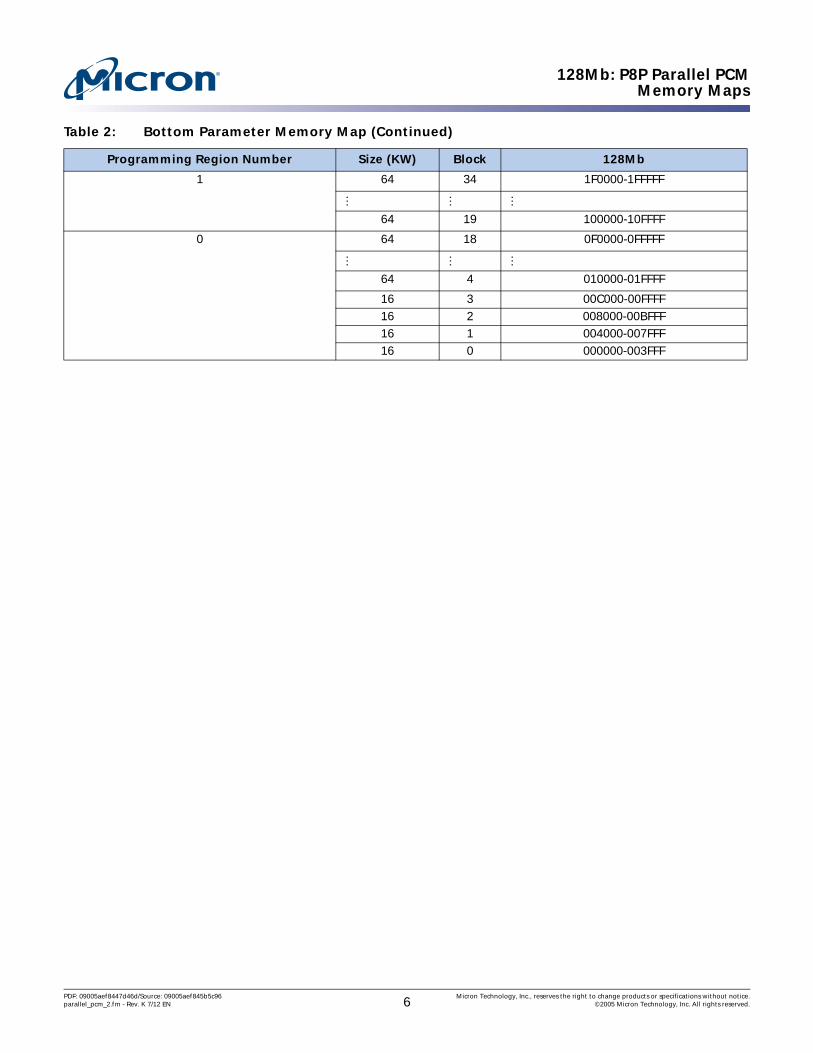
Table 2: Bottom Parameter Memory Map
Programming Region Number Size (KW) Block 128Mb
7 64 130 7F0000-7FFFFF
… … …
64 115 700000-70FFFF
6 64 114 6F0000-6FFFFF
… … …
64 99 600000-60FFFF
5 64 98 5F0000-5FFFFF
… … …
64 83 500000-50FFFF
4 64 82 4F0000-4FFFFF
… … …
64 67 400000-40FFFF
3 64 66 3F0000-3FFFFF
… … …
64 51 300000-30FFFF
2 64 50 2F0000-2FFFFF
… … …
64 35 200000-20FFFF
Table 1: Top Parameter Memory Map (Continued)
Programming Region Number Size (KW) Block 128Mb
PDF: 09005aef8447d46d/Source: 09005aef845b5c96 Micron Technology, Inc., reserves the right to change products or specifications without notice.parallel_pcm_2.fm - Rev. K 7/12 EN 5 ©2005 Micron Technology, Inc. All rights reserved.
128Mb: P8P Parallel PCMMemory Maps
1 64 34 1F0000-1FFFFF
… … …
64 19 100000-10FFFF
0 64 18 0F0000-0FFFFF
… … …
64 4 010000-01FFFF
16 3 00C000-00FFFF16 2 008000-00BFFF16 1 004000-007FFF16 0 000000-003FFF
Table 2: Bottom Parameter Memory Map (Continued)
Programming Region Number Size (KW) Block 128Mb
PDF: 09005aef8447d46d/Source: 09005aef845b5c96 Micron Technology, Inc., reserves the right to change products or specifications without notice.parallel_pcm_2.fm - Rev. K 7/12 EN 6 ©2005 Micron Technology, Inc. All rights reserved.

128Mb: P8P Parallel PCMPackage Dimensions
Package Dimensions
TSOP Mechanical Specifications
Figure 1: 56-Lead TSOP
Notes: 1. One dimple on package denotes pin 1.2. If two dimples exist, then the larger dimple denotes pin 1.3. Pin 1 will always be in the upper left corner of the package, in reference to the product
mark.
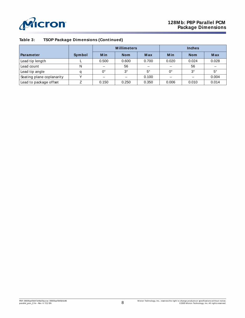
Table 3: TSOP Package Dimensions
Parameter Symbol
Millimeters Inches
Min Nom Max Min Nom Max
Package height A – – 1.200 – – 0.047
Standoff A1 0.050 – – 0.002 – –
Package body thickness A2 0.965 0.995 1.025 0.038 0.039 0.040
Lead width b 0.100 0.150 0.200 0.004 0.006 0.008
Lead thickness c 0.100 0.150 0.200 0.004 0.006 0.008
Package body length D1 18.200 18.400 18.600 0.717 0.724 0.732
Package body width E 13.800 14.000 14.200 0.543 0.551 0.559
Lead pitch e – 0.500 – – 0.0197 –
Terminal dimension D 19.800 20.00 20.200 0.780 0.787 0.795
See Detail A
0.5 TYP
14.00 ±0.2
0.25 ±0.1
1.20 MAX
18.4 ±0.2 0.995 ±0.03
20 ±0.2
0.15 ±0.05
Detail A0.60 ±0.10
0.05 MIN
0.10
Seatingplane
Pin #1 index
See notes 2and 4
See note 3 See note 3
See note 3
0.15 ±0.05
3° +2°-3°
PDF: 09005aef8447d46d/Source: 09005aef845b5c96 Micron Technology, Inc., reserves the right to change products or specifications without notice.parallel_pcm_2.fm - Rev. K 7/12 EN 7 ©2005 Micron Technology, Inc. All rights reserved.
128Mb: P8P Parallel PCMPackage Dimensions
Lead tip length L 0.500 0.600 0.700 0.020 0.024 0.028
Lead count N – 56 – – 56 –
Lead tip angle q 0° 3° 5° 0° 3° 5°
Seating plane coplanarity Y – – 0.100 – – 0.004
Lead to package offset Z 0.150 0.250 0.350 0.006 0.010 0.014
Table 3: TSOP Package Dimensions (Continued)
Parameter Symbol
Millimeters Inches
Min Nom Max Min Nom Max
PDF: 09005aef8447d46d/Source: 09005aef845b5c96 Micron Technology, Inc., reserves the right to change products or specifications without notice.parallel_pcm_2.fm - Rev. K 7/12 EN 8 ©2005 Micron Technology, Inc. All rights reserved.

128Mb: P8P Parallel PCMPackage Dimensions
64-Ball Easy BGA Package
Figure 2: 64-Ball Easy BGA Package
Table 4: Easy BGA Package Dimensions
Parameter Symbol
Millimeters
Min Nom Max
Package height (128Mb) A – – 1.20
Ball height A1 0.25 – –
Package body thickness (128Mb) A2 – 0.78 –
Ball (lLead) width b 0.33 0.43 0.53
Package body width D 9.90 10.00 10.10
Package body length E 7.90 8.00 8.10
Pitch e – 1.00 –
Ball (lead) count N – 64 –
Seating plane coplanarity Y – – 0.10
Corner to ball A1 distance along D S1 1.40 1.50 1.60
Corner to ball A1 distance along E S2 0.49 0.50 0.51
Ball A1 ID
0.78 TYP
Seatingplane
0.1
1.20 MAX
1.00 TYP
A
B
C
D
E
F
G
H
8 7 6 5 4 3 2 1
0.5 ±0.1
10 ±0.1
64X Ø0.43 ±0.1
1.00 TYP
8 ±0.1
1.5 ±0.1 Ball A1 ID
PDF: 09005aef8447d46d/Source: 09005aef845b5c96 Micron Technology, Inc., reserves the right to change products or specifications without notice.parallel_pcm_2.fm - Rev. K 7/12 EN 9 ©2005 Micron Technology, Inc. All rights reserved.
128Mb: P8P Parallel PCMPinouts and Ballouts
Pinouts and Ballouts
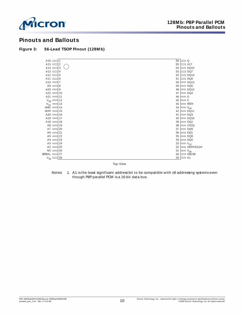
Figure 3: 56-Lead TSOP Pinout (128Mb)
Notes: 1. A1 is the least significant address bit to be compatible with x8 addressing systems even though P8P parallel PCM is a 16-bit data bus.
12345678910111213141516171819202122232425262728
A16A15A14A13A12A11A10
A9A23A22A21VSSVCC
WE#WP#A20A19A18
A8A7A6A5A4A3A2NC
SERIALVSS
QA17DQ15DQ7DQ14DQ6DQ13DQ5DQ12DQ4DCRST#VPPDQ11DQ3DQ10DQ2VCCQDQ9DQ1DQ8DQ0VCCOE#/HOLD#VSSCE#/S#A1
56555453525150494847464544434241403938373635343332313029
Top View
PDF: 09005aef8447d46d/Source: 09005aef845b5c96 Micron Technology, Inc., reserves the right to change products or specifications without notice.parallel_pcm_2.fm - Rev. K 7/12 EN 10 ©2005 Micron Technology, Inc. All rights reserved.

128Mb: P8P Parallel PCMPinouts and Ballouts
Figure 4: 64-Ball Easy BGA Ballout (128Mb)
Notes: 1. A1 is the least significant address bit to be compatible with x8 addressing systems even though P8P parallel PCM is a 16-bit data bus.
1
A1
A2
A3
A4
D8
SERIAL
A23
RFU
1
A1
A2
A3
A4
D8
SERIAL
A23
RFU
8
A22
RFU
A21
A17
RFU
OE#/HOLD#
WE#
RFU
8
A22
RFU
A21
A17
RFU
OE#/HOLD#
WE#
RFU
3
A8
A9
A10
A11
D9
D10
D2
VCC
3
A8
A9
A10
A11
D9
D10
D2
VCC
4
VPP
CE#/SE#
A12
RST#
D3
D11
VCCQ
VSS
4
VPP
CE#/SE#
A12
RST#
D3
D11
VCCQ
VSS
5
A13
A14
A15
VCCQ
D4
D12
D5
D13
5
A13
A14
A15
VCCQ
D4
D12
D5
D13
6
VCC
RFU
WP#
VCCQ
C
D
D6
VSSQ
6
VCC
RFU
WP#
VCCQ
C
D
D6
VSSQ
7
A18
A19
A20
A16
D15
Q
D14
D7
7
A18
A19
A20
A16
D15
Q
D14
D7
Easy BGATop view-ball side down
Easy BGATop view-ball side up
A
B
C
D
E
F
G
H
A
B
C
D
E
F
G
H
2
A6
VSS
A7
A5
D1
D0
RFU
VSSQ
2
A6
VSS
A7
A5
D1
D0
RFU
VSSQ
PDF: 09005aef8447d46d/Source: 09005aef845b5c96 Micron Technology, Inc., reserves the right to change products or specifications without notice.parallel_pcm_2.fm - Rev. K 7/12 EN 11 ©2005 Micron Technology, Inc. All rights reserved.

128Mb: P8P Parallel PCMSignal Names and Descriptions
Signal Names and Descriptions
Table 5: Ball/Pin Descriptions
Symbol Type Desctiption
A[MAX:1] Input Address inputs: Device address inputs. 128Mb: A[23:1]. The address bus for TSOP and easy BGA starts at A1. P8P parallel PCM uses x16 addressing. The P8P parallel PCM package is x8 addressing and is compatible with J3 or P30 products.
DQ[15:0] Input/Output
Data input/outputs: Inputs data and commands during WRITEs (internally latched). Outputs data during READ operations. Data signals float when CE# or OE# are VIH or RST# is VIL.
CE# or S# Input Chip enable: CE# LOW activates internal control logic, I/O buffers, decoders, and sense amps. CE# HIGH deselects the device, places it in standby state, and places data outputs at High-Z.
SPI SPI select: S# LOW activates WRITE commands to the SPI interface. Raising S# to VIH completes (or terminates) the SPI command cycle; it also sets Q to High-Z.
OE# or HOLD#
Input Output enable: Active LOW OE# enables the device’s output data buffers during a READ cycle. With OE# at VIH, device data outputs are placed in High-Z state.
SPI SPI HOLD#: When asserted, suspends the current cycle and sets Q to High-Z until de-asserted.RST# Input Reset chip: When LOW, RST# resets internal automation and inhibits WRITE operations. This
provides data protection during power transitions. RST# HIGH enables normal operation. The device is in 8-word page mode array read after reset exits.
WE# Input Write enable: controls command user interface (CUI) and array WRITEs. Its rising edge latches addresses and data.
WP# Input Write protect: Disables/enables the lock-down function. When WP# is VIL, the lock-down mechanism is enabled and software cannot unlock blocks marked lock-down. When WP# is VIH, the lock-down mechanism is disabled and blocks previously locked-down are now locked; software can unlock and lock them. After WP# goes LOW, blocks previously marked lock-down revert to that state.
C SPI SPI clock: Synchronization clock for input and output dataD SPI SPI data input: Serial data input for op codes, address, and program data bytes. Input data is
clocked in on the rising edge of C, starting with the MSB.Q SPI SPI data output: Serial data output for read data. Output data is clocked out, triggered by the
falling edge of C, starting with the MSB.SERIAL SPI SPI enable: SERIAL is a port select switching between the normal parallel or serial interface. When
VSS, the normal (non-SPI) P8P parallel PCM interface, is enabled, all other SPI inputs are “Don't Care,” and Q is at High-Z. When VCC SPI mode is enabled, all non-SPI inputs are “Don't Care,” and all outputs are at High-Z. This pin has an internal weak pull-down resistor to select the normal parallel interface when users leave the pin floating. A CAM can be used to permanently disable this feature.
VPP Pwr Erase and write power: A valid VPP voltage enables erase or programming. Memory contents can’t be altered when VPP VPPLK.Set VPP = VCC for in-system PROGRAM and ERASE operations. To accommodate resistor or diode drops from the system supply, the VIH level of VPP can be as low as VPPL,min. Program/erase voltage is normally 1.7–3.6V.
VCC Pwr Device power supply: WRITEs are inhibited at VCC VLKO. Device operations at invalid VCC voltages should not be attempted.
VCCQ Pwr Output power supply: Enables all outputs to be driven at VCCQ. This input may be tied directly to VCC if VCCQ is to function within the VCC range.
VSS Pwr Ground: Connects device circuitry to system ground.VSSQ Pwr I/O ground: Tie to GND.NC No connect: No internal connection; can be driven or floated.DU Don’t use: Don’t connect to power supply or other signals.RFU Reserved for future use: Don’t connect to other signals.
PDF: 09005aef8447d46d/Source: 09005aef845b5c96 Micron Technology, Inc., reserves the right to change products or specifications without notice.parallel_pcm_2.fm - Rev. K 7/12 EN 12 ©2005 Micron Technology, Inc. All rights reserved.

128Mb: P8P Parallel PCMBus Operations
Bus OperationsCE# at VIL and RST# at VIH enables device READ operations. Assume addresses are always valid. OE# LOW activates the outputs and gates selected data onto the I/O bus. WE# LOW enables device WRITE operations. When the VPP voltage VPPLK (lock-out voltage), only READ operations are enabled.
Notes: 1. See Table 8 on page 16 for valid DIN during a WRITE operation.2. X = “Don’t Care) (L or H).3. OE# and WE# should never be asserted simultaneously. If this occurs, OE# overrides WE#.
READ Operations
To perform a READ operation, RST# and WE# must be de-asserted while CE# and OE# are asserted. CE# is the device select control. When asserted, it enables the Flash memory device. OE# is the data output control. When asserted, the addressed Flash memory data is driven onto the I/O bus.
WRITE Operations
To perform a WRITE operation, both CE# and WE# are asserted while RST# and OE# are de-asserted. During a WRITE operation, address and data are latched on the rising edge of WE# or CE#, whichever occurs first. Table 7 on page 14 describes the bus cycle sequence for each of the supported device commands, and Table 8 on page 16 describes each command. See “AC Characteristics” on page 48 for signal timing details.
Notes: 1. WRITE operations with invalid VCC and/or VPP voltages can produce spurious results and should not be attempted.
OUTPUT DISABLE Operations
When OE# is de-asserted, device outputs DQ[15:0] are disabled and placed in High-Z; WAIT is also placed in High-Z.
STANDBY Operations
When CE# is de-asserted, the device is deselected and placed in standby, substantially reducing power consumption. In standby, the data outputs are placed in High-Z, inde-pendent of the level placed on OE#. Standby current, ICCS, is the average current measured over any 5ms time interval, 5µs after CE# is de-asserted. During standby, average current is measured over the same time interval 5µs after CE# is de-asserted.
When the device is deselected (while CE# is de-asserted) during a PROGRAM or ERASE operation, it continues to consume active power until the PROGRAM or ERASE opera-tion is completed.
Table 6: Bus Operations
State RST# CE# OE# WE# DQ[15:0] Notes
READ (main array) VIH VIL VIL VIH DOUT
READ (status, query, identifier) VIH VIL VIL VIH DOUT
OUTPUT DISABLE VIH VIL VIH VIH High-Z
STANDBY VIH VIH X X High-Z 2
RESET VIL X X X High-Z 2
WRITE VIH VIL VIH VIL DIN 1
PDF: 09005aef8447d46d/Source: 09005aef845b5c96 Micron Technology, Inc., reserves the right to change products or specifications without notice.parallel_pcm_2.fm - Rev. K 7/12 EN 13 ©2005 Micron Technology, Inc. All rights reserved.

128Mb: P8P Parallel PCMCommand Set
RESET Operations
As with any automated device, it is important to assert RST# when the system is reset. When the system comes out of reset, the system processor attempts to read from the Flash memory if it is the system boot device. If a CPU reset occurs with no Flash memory reset, improper CPU initialization may occur because the Flash memory may be providing status information rather than array data. Micron Flash memory devices enable proper CPU initialization following a system reset using the RST# input. RST# should be controlled by the same low true RESET signal that resets the system CPU.
After initial power-up or reset, the device defaults to asynchronous read array mode, and the status register is set to 0x80. Asserting RST# de-energizes all internal circuits and places the output drivers in High-Z. When RST# is asserted, the device shuts down the operation in progress, a process that takes a minimum amount of time to complete. When RST# has been de-asserted, the device is reset to asynchronous read array state.
Note: If RST# is asserted during a PROGRAM or ERASE operation, the operation is termi-nated, and the memory contents at the aborted location (for a PROGRAM) or block (for an ERASE) are no longer valid because the data may have been only partially writ-ten or erased.
When returning from a reset (RST# de-asserted), a minimum wait is required before the initial read access outputs valid data. Also, a minimum delay is required after a reset before a WRITE cycle can be initiated. After this wake-up interval passes, normal opera-tion is restored. See “AC Characteristics” on page 48 for details about signal timing.
Command Set
Device Command Codes
The system CPU provides control of all in-system READ, WRITE, and ERASE operations of the device via the system bus. The on-chip write state machine (WSM) manages all block erase and word program algorithms.
Device commands are written to the command user interface (CUI) to control all Flash memory device operations. The CUI does not occupy an addressable memory location; it is the mechanism through which the Flash device is controlled.
Table 7: Command Codes and Descriptions
Mode Code Command Description
Read FFh READ ARRAY Places device in read array mode so that data signals output array data on DQ[15:0].70h READ STATUS
REGISTERPlaces the device in status register read mode. Status data is output on DQ[7:0]. The device automatically enters this mode after a PROGRAM or ERASE command is issued to it.
90h READ ID CODE Puts the device in read identifier mode. Device reads from the addresses output manufacturer/device codes, block lock status, or protection register data on DQ[15:0].
98h READ QUERY Puts the device in read query mode. Device reads from the address given outputting the common Flash interface information on DQ[7:0].
50h CLEAR STATUS REGISTER
The WSM can set the status register’s block lock (SR1), VPP (SR3), program (SR4), and erase (SR5) status bits to 1, but cannot clear them. Device reset or the CLEAR STATUS REGISTER command at any device address clears those bits to 0.
PDF: 09005aef8447d46d/Source: 09005aef845b5c96 Micron Technology, Inc., reserves the right to change products or specifications without notice.parallel_pcm_2.fm - Rev. K 7/12 EN 14 ©2005 Micron Technology, Inc. All rights reserved.

128Mb: P8P Parallel PCMCommand Set
Notes: 1. Do not use unassigned (reserved) commands.
Program 40h PROGRAMSET-UP
This preferred program command’s first cycle prepares the CUI for a PROGRAM operation. The second cycle latches address and data and executes the WSM program algorithm at this location. Status register updates occur when CE# or OE# is toggled. A READ ARRAY command is required to read array data after programming.
10h ALT SET-UP Equivalent to a PROGRAM SET-UP command (40h).42h BIT-ALTERABLE
WRITEThe command sequence is the same as WORD PROGRAM (40h). The difference is that the state of the PCM memory cell can change from a 0 to 1 or 1 to 0, unlike a Flash memory cell, which can only change from 1 to 0 during programming.
E8h BUFFERED PROGRAM
This command loads a variable number of bytes up to the buffer size 32 words onto the program buffer.
EAh BIT-ALTERABLE BUFFERED
WRITE
This command sequence is the similar to BUFFERED PROGRAM, but the BUFFER WRITE command is bit alterable or overwrite operation. The command sequence is the same as E8h.
DEh BUFFER PROGRAM ON
ALL 1s
This command is the same as BUFFERED PROGRAM, but the user indicates that the page is already set to all 1s. The command sequence is the same as E8h
D0h BUFFERED WRITE
CONFIRM
The confirm command is issued after the data streaming for writing into the buffer is done. This initiates the WSM to carry out the buffered programing algorithm.
Erase 20h BLOCK ERASE SET-UP
Prepares the CUI for block erase. The device emulates erasure of the block addressed by the ERASE CONFIRM command by writing all 1s. If the next command is not ERASE CONFIRM:The CUI sets status register bits SR4 and SR5 to 1.The CUI places the device in the read status register mode.The CUI waits for another command.
D0h ERASE CONFIRM
If the first command was ERASE SET-UP (20h), the CUI latches address and data, and then emulates erasure of the block indicated by the ERASE CONFIRM cycle address.
Suspend B0h WRITE SUSPEND or
ERASE SUSPEND
This command issued at any device address initiates suspension of the currently executing PROGRAM/ERASE operation. The status register, invoked by a READ STATUS REGISTER command, indicates successful SUSPEND operation by setting status bits SR2 (write suspend) or SR6 (erase suspend) and SR7. The WSM remains in suspend mode regardless of the control signal states, except RST# = VIL.
D0h SUSPEND RESUME
This command issued at any device address resumes suspended PROGRAM or ERASE operation.
Block Locking
60h LOCK SET-UP Prepares the CUI for lock configuration. If the next command is not BLOCK LOCK, UNLOCK, or LOCK-DOWN the CUI sets SR4 and SR5 to indicate command sequence error.
01h LOCK BLOCK If the previous command was LOCK SET-UP (60h), the CUI locks the addressed block.D0h UNLOCK
BLOCKAfter a LOCK SET-UP (60h) command, the CUI latches the address and unlocks the addressed block.
2Fh LOCK-DOWN After a LOCK SET-UP (60h) command, the CUI latches the address and locks down the addressed block.
Protection C0h PROTECTION PROGRAM
SET-UP
Prepares the CUI for a protection register program operation. The second cycle latches address and data and starts the WSM’s protection register program or lock algorithm. Toggling CE# or OE# updates the PCM status register data. To read array data after programming, issue a READ ARRAY command.
Table 7: Command Codes and Descriptions (Continued)
Mode Code Command Description
PDF: 09005aef8447d46d/Source: 09005aef845b5c96 Micron Technology, Inc., reserves the right to change products or specifications without notice.parallel_pcm_2.fm - Rev. K 7/12 EN 15 ©2005 Micron Technology, Inc. All rights reserved.

128Mb: P8P Parallel PCMDevice Command Bus Cycles
Device Command Bus CyclesDevice operations are initiated by writing specific device commands to the CUI. Several commands, including WORD PROGRAM and BLOCK ERASE, are used to modify array data commands. Writing either command to the CUI initiates a sequence of internally timed functions that culminate in the completion of the requested task. However, the operation can be aborted either by asserting RST# or by issuing an appropriate SUSPEND command.
Notes: 1. First command cycle address should be the same as the operation’s target address.X = Any valid address within the deviceIA = Identification code addressBA = Address within the blockLPA = Lock protection address (from the CFI); P8P parallel PCM LPA is at 0080hPA = 4-word protection address in the user-programmable area of device identification planeDnA = Address within the deviceDBA = Device base address: (A[MAX:1] = 0h)PRA = Program regionQA = Query code addressWA = Word address of memory location to be written
2. SRD = Data read from the status registerWD = Data to be written at location WAID = Identifier code dataPD = User-programmable protection dataQD = Query code data on DQ[7:0]N = Data count to be loaded into the device to indicate how many words would be written
Table 8: Command Sequences in x16 Bus Mode
Mode CommandBus
Cycles
First Bus Cycle Second Bus Cycle
Oper Addr1 Data2 Oper Addr1 Data2
Read READ ARRAY/RESET 1 WRITE DnA FFh – – –
READ DEVICE IDENTIFIERS 2 WRITE DnA 90h READ DBA+IA ID
READ QUERY 2 WRITE DnA 98h READ DBA+QA QD
READ STATUS REGISTER 2 WRITE BA 70h READ BA SRD
CLEAR STATUS REGISTER 1 WRITE X 50h – – –Program PROGRAM 2 WRITE WA 40h or
10hWRITE WA WD
BIT-ALTERABLE PROGRAM 2 WRITE WA 42h WRITE PA PD
BUFFERED PROGRAM3 2 WRITE WA E8h WRITE WA N-1
BIT-ALTERABLE BUFFERED PROGRAM3
> 2 WRITE WA EAh WRITE WA N-1
BUFFERED PROGRAM ON ALL1s > 2 WRITE WA DEh WRITE WA N-1Erase BLOCK ERASE 2 WRITE BA 20h WRITE BA D0h
Suspend PROGRAM/ERASE SUSPEND 1 WRITE X B0h – – –
PROGRAM/ERASE RESUME 1 WRITE X D0h – – –BlockLock
LOCK BLOCK 2 WRITE BA 60h WRITE BA 01h
UNLOCK BLOCK 2 WRITE BA 60h WRITE BA D0h
LOCK-DOWN BLOCK 2 WRITE BA 60h WRITE BA 2FhProtection PROTECTION PROGRAM 2 WRITE PA C0h WRITE PA PD
LOCK PROTECTION PROGRAM 2 WRITE LPA C0h WRITE LPA FFFDh
PDF: 09005aef8447d46d/Source: 09005aef845b5c96 Micron Technology, Inc., reserves the right to change products or specifications without notice.parallel_pcm_2.fm - Rev. K 7/12 EN 16 ©2005 Micron Technology, Inc. All rights reserved.
128Mb: P8P Parallel PCMREAD Operations
into the buffer; because the internal registers count from 0, the user writes N - 1 to load N words.
3. The second cycle of the BUFFERED PROGRAM command, which is the count being loaded into the buffer, is followed by data streaming up to 32 words, and then a CONFIRM com-mand is issued that triggers the programming operation. Refer to “Figure 33 on page 61.”
READ OperationsP8P parallel PCM has several read modes: • Read array mode returns PCM array data from the addressed locations.• Read identifier mode returns manufacturer device identifier data, block lock status,
and protection register data. • Read query mode returns device CFI (or query) data. • Read Status Register mode returns the device status register data. A system processor
can check the status register to determine the device’s state or to monitor program or erase progress.
READ ARRAY
The READ ARRAY command places (or resets) the device to read array mode. Upon initial device power-up or after reset (RST# transitions from VIL to VIH), the device defaults to read array mode. If an ERASE or PROGRAM SUSPEND command suspends the WSM, a subsequent READ ARRAY command will place the device in read array mode. The READ ARRAY command functions independently of VPP voltage.
PDF: 09005aef8447d46d/Source: 09005aef845b5c96 Micron Technology, Inc., reserves the right to change products or specifications without notice.parallel_pcm_2.fm - Rev. K 7/12 EN 17 ©2005 Micron Technology, Inc. All rights reserved.

128Mb: P8P Parallel PCMREAD Operations
READ IDENTIFIER
The read identifier mode is used to access the manufacturer/device identifier, block lock status, and protection register codes. The identifier space occupies the address range supplied by the READ IDENTIFIER command (90h) address.
Notes: 1. DBA = Device base address: (A[MAX:18] = DBA). Micron reserves other configuration address locations.
2. BBA = Block base address.
READ QUERY
The query space comes to the foreground and occupies the device address range supplied by the READ QUERY command address. The mode outputs CFI data when the device addresses are read. “Common Flash Interface” on page 73 describes the query mode information and addresses. Write the READ ARRAY command to return to read array mode. The read performance of this CFI data follows the same timings as the main array.
In addition to other ID mode data, the protection registers (such as block locking infor-mation and the device JEDEC ID) may be accessed as long as there are no ongoing WRITE or ERASE operations.
Table 9: Read Identifier Table
Parameter Address1, 2 Data
Manufacturer code DBA + 000000h0089h
Device code DBA + 000001h ID (see Table 10 on page 18)
Block lock configuration BBA + 000002h Lock
Block Is unlocked DQ0 = 0
Block Is locked DQ0 = 1
Block Is not locked down DQ1 = 0
Block Is locked down DQ1 = 1
Reserved for future use DQ[7:2]
Lock protection register 0 DBA + 000080h PR-LK0
64-bit factory-programmable protection register
DBA + 000081h–000084h Protection register data
64-bit user-programmable protection register
DBA + 000085h–000088h Protection register data
Lock protection register 1 DBA + 000089h PR-LK1
16 x 128-bit user-programmable protection registers
DBA + 00008Ah–0000109h Protection register data
Table 10: Device Codes
Device
Device Code (Byte/Word)
ModeHex
Binary
High Byte Low Byte
128Mb 881E 10001000 00011110 Top boot128Mb 8821 10001000 00100001 Bottom boot
PDF: 09005aef8447d46d/Source: 09005aef845b5c96 Micron Technology, Inc., reserves the right to change products or specifications without notice.parallel_pcm_2.fm - Rev. K 7/12 EN 18 ©2005 Micron Technology, Inc. All rights reserved.

128Mb: P8P Parallel PCMPROGRAM Operations
Query (CFI) data is read by sending the READ QUERY command to the device. Reading the query data is subject to the same restrictions as reading the protection registers.
PROGRAM OperationsFive WRITE operations are available in P8P parallel PCM. • WORD PROGRAM (40h, or 10h)• BIT-ALTERABLE WORD WRITE (42h)• BUFFERED PROGRAM (E8h)• BIT-ALTERABLE BUFFERED WRITE (EAh)• BUFFERED PROGRAM ON ALL 1s (DEh)
Writing a PROGRAM command to the device initiates internally timed sequences that write the requested word. The WSM executes a sequence of internally timed events to write desired bits at the addressed location and to verify that the bits are sufficiently written. For word programming, the memory changes specifically addressed bits to 0; 1 bits do not change the memory cell contents. This enables individual data bits to be programmed (0) while 1 bits serve as data masks. For BIT-ALTERABLE WORD WRITE, the memory cell can change from 0 to 1 or 1 to a 0.
The status register can be examined for write progress and errors by reading any address within the device during a WRITE operation. Issuing a READ STATUS REGISTER command brings the status register to the foreground enabling write progress to be monitored or detected at other device addresses. Status register bit SR7 indicates device write status while the write sequence executes. CE# or OE# toggle (during polling) updates the status register. Valid commands that can be issued to the writing device during write include READ STATUS REGISTER, WRITE SUSPEND, READ IDENTIFIER, READ QUERY, and READ ARRAY; however, READ ARRAY will return unknown data while the device is busy.
When writing completes, status register bit SR4 indicates write success if zero (0) or failure if set (1). If SR3 is set (1), the WSM couldn’t execute the WRITE command because VPP was outside acceptable limits. If SR1 is set (1), the WRITE operation targeted a locked block and was aborted. Attempting to write in an erase suspended block will result in failure, and SR4 will be set (1).
After examining the status register, clear it by issuing the CLEAR STATUS REGISTER command before issuing a new command. The device remains in status register mode until another command is written to that device. Any command can follow after writing completes.
WORD PROGRAM
The system processor writes the WORD PROGRAM SETUP command (40h/10h) to the device followed by a second WRITE that specifies the address and data to be programmed. The device accessed during both of the command cycles automatically outputs status register data when the device address is read. The device accessed during the second cycle (the data cycle) of the program command sequence will be where the data is programmed. See Figure 33 on page 61.
When VPP is greater than VPPLK, program and erase currents are drawn through the VCC input. If VPP is driven by a logic signal, VPP must remain above VPP,min to perform in-system PCM modifications. Figure 5 on page 22 shows PCM power supply usage in various configurations.
PDF: 09005aef8447d46d/Source: 09005aef845b5c96 Micron Technology, Inc., reserves the right to change products or specifications without notice.parallel_pcm_2.fm - Rev. K 7/12 EN 19 ©2005 Micron Technology, Inc. All rights reserved.

128Mb: P8P Parallel PCMPROGRAM Operations
BIT-ALTERABLE WORD WRITE
The BIT-ALTERABLE WORD WRITE command executes just like the WORD PROGRAM command (40h/10h), using a two-write command sequence. The BIT-ALTERABLE WRITE SETUP command (42h) is written to the CUI, followed by the specific address and data to be written. The WSM will start executing the programming algorithm, but the data written to the CUI will be directly overwritten into the PCM memory. This is unlike Flash memory, which can only be written from 1 to 0 without a prior erase of the entire block. See Table 12 on page 21. This overwrite function eliminates Flash bit masking, which means that the software cannot use a 1 in a data mask to produce no change of the memory cell, as might occur with floating gate Flash.
BUFFERED PROGRAM
A BUFFERED PROGRAM command sequence initiates the loading of a variable number of words, up to the buffer size (32 words), into the program buffer and then into the PCM device. First, the BUFFERED PROGRAM SETUP command is issued along with the BLOCK ADDRESS (Figure 33 on page 61). When status register bit SR7 is set to 1, the buffer is ready for loading. Now a word count is given to the part with the block address.
On the next write, a device starting address is given along with the program buffer data. Subsequent writes provide additional device addresses and data, depending on the count. All subsequent addresses must lie within the starting address plus the buffer size. Maximum programming performance and lower power are obtained by aligning the starting address at the beginning of a 32-word boundary. A misaligned starting address is not allowed and results in invalid data. After the final buffer data is given, a PROGRAM BUFFER CONFIRM command is issued. This initiates the WSM to begin copying the buffer data to the PCM array.
If a command other than BUFFERED PROGRAM CONFIRM command (D0h) is written to the device, an invalid command/sequence error will be generated, and status register bits SR5 and SR4 will be set to a 1. For additional buffer writes, issue another PROGRAM BUFFER SETUP command and check SR7. If an error occurs while writing, the device will stop writing, and status register bit SR4 will be set to a 1 to indicate a program failure. The internal WSM verify only detects errors for 1s that do not successfully program to 0s.
If a program error is detected, the status register should be cleared by the user before issuing the next PROGRAM command. Additionally, if the user attempts to program past the block boundary with a PROGRAM BUFFER command, the device will abort the PROGRAM BUFFER operation. This will generate an invalid command/sequence error and status register bits SR5 and SR4 will be set to a 1. All bus cycles in the buffered programming sequence should be addressed to the same block. If a buffered program-ming is attempted while the VPP VPPLK, status register bits SR4 and SR3 will be set to 1.
Buffered write attempts with invalid VCC and VPP voltages produce spurious results and should not be attempted. Buffered program operations with VIH < RST# < VHH may produce spurious results and should not be attempted.
Successful programming requires that the addressed block’s locking status to be cleared. If the block is locked down, then the WP# pin must be raised HIGH, and then the block could be unlocked to execute a PROGRAM operation. An attempt to program a locked block results in setting of SR4 and SR1 to a 1 (for example, error in programming).
PDF: 09005aef8447d46d/Source: 09005aef845b5c96 Micron Technology, Inc., reserves the right to change products or specifications without notice.parallel_pcm_2.fm - Rev. K 7/12 EN 20 ©2005 Micron Technology, Inc. All rights reserved.

128Mb: P8P Parallel PCMPROGRAM Operations
BIT-ALTERABLE BUFFER WRITE
The BIT-ALTERABLE BUFFER WRITE command sequence is the same as for BUFFER PROGRAM. For command sequence, see “BUFFERED PROGRAM” on page 20. The primary difference between the two buffer commands is when the WSM starts executing, the data written to the buffer will be directly overwritten into the PCM memory, unlike Flash Memory, which can only go from 1 to 0 before an erase of the entire block. See Table 12 on page 21. This overwrite function eliminates Flash bit masking, which means software cannot use a 1 in a data mask for no change of the memory cell, as might occur with floating gate Flash.
The advantage of bit alterability is that no block erase is needed prior to writing a block, which minimizes system overhead for software management of data and ultimately improves latency and determinism and reduces power consumption because of reduc-tion of system overhead. Storing counter variables can easily be handled using PCM memory because a 0 can change to a 1 or a 1 can change to a 0.
BIT-ALTERABLE BUFFER PROGRAM
This mode is sometimes referred to as PRESET BUFFERED PROGRAM.
PROGRAM ON ALL 1s is similar to program mode (1s treated as masks; 0s written to cells) with the assumption that all the locations in the addressed page have previously been set (1s). Performance of BUFFER PROGRAM ON ALL 1s expected to be better than buffered program mode because the preread step before programming is eliminated. The command sequence for BUFFERED PROGRAM ON ALL 1s is the same as BUFF-ERED PROGRAM command (E8h).
PROGRAM SUSPEND
Issuing the PROGRAM SUSPEND command while programming suspends the program-ming operation. This enables data to be accessed from the device other than the one being programmed. The PROGRAM SUSPEND command can be issued to any device address. A PROGRAM operation can be suspended to perform reads only. Additionally, a PROGRAM operation that is running during an ERASE SUSPEND can be suspended to perform a READ operation.
Table 11: Buffered Programming and Bit-Alterable Buffer Write Timing Requirements
Alignment Programming Time Example
32-word/64-byte aligned tPROG/PB Start address = 1FFF10h; end address = 1FFF2Fh
Table 12: Bit Alterability vs. Flash Bit-Masking
ProgrammingFunction
CommandIssued
Memory CellCurrent State
Data FromUser
Memory CellAfter Programming
Flash bit masking 40h or E8h 0 0 040h or E8h 0 1 040h or E8h 1 0 040h or E8h 1 1 1
Bit alterability 42h or EAh 0 0 042h or EAh 0 1 142h or EAh 1 0 042h or EAh 1 1 1
PDF: 09005aef8447d46d/Source: 09005aef845b5c96 Micron Technology, Inc., reserves the right to change products or specifications without notice.parallel_pcm_2.fm - Rev. K 7/12 EN 21 ©2005 Micron Technology, Inc. All rights reserved.

128Mb: P8P Parallel PCMERASE
When a programming operation is executing, issuing the PROGRAM SUSPEND command requests the WSM to suspend the programming algorithm at predetermined points. The device continues to output status register data after the PROGRAM SUSPEND command is issued. Programming is suspended when status register bits SR[7,2] are set.
To read data from the device, the READ ARRAY command must be issued. READ ARRAY, READ STATUS REGISTER, READ DEVICE IDENTIFIER, READ CFI, and PROGRAM RESUME are valid commands during a PROGRAM SUSPEND.
During a PROGRAM SUSPEND, de-asserting CE# places the device in standby, reducing active current. VPP must remain at its programming level, and WP# must remain unchanged while in PROGRAM SUSPEND. If RST# is asserted, the device is reset.
PROGRAM RESUME
The RESUME command instructs the device to continue programming, and automati-cally clears Status Register bits SR[7,2]. This command can be written to any address. If error bits are set, the Status Register should be cleared before issuing the next instruc-tion. RST# must remain de-asserted.
PROGRAM PROTECTION
Holding the VPP input at VIL provides absolute hardware write protection for all PCM device blocks. If VPP is below VPPLK, WRITE or ERASE operations halt and an error is posted in status register bit SR3. The block lock registers are not affected by the VPP level; they may be modified and read even if VPP is below VPPLK.
Figure 5: Example VPP Power Supply Configuration
ERASEUnlike floating gate Flash, PCM does not require a high-voltage BLOCK ERASE operation to change all the bits in a block to 1. As a bit-alterable technology, each bit is capable of independently being changed from a 0 to a 1 and from a 1 to a 0. With floating gate Flash, a high voltage potential must be placed in parallel upon a group of bits called an erase block. Each bit within the block may be changed independently from 1 to a 0, but only
VCCVPP
System supply System supply
System supply
PROT# (logic signal)
System supply
VPP
• VPP supply during factory programming• Complete write/erase protection: VPP ≤ VPPLK
VCC
VPP
• Low-Voltage programming• Absolute write protection via logic signal
VCC
VPP
• Low-voltage and VPP factory programming
VCC
VPP
• Low-Voltage programming
≤10kΩ
VPP
PDF: 09005aef8447d46d/Source: 09005aef845b5c96 Micron Technology, Inc., reserves the right to change products or specifications without notice.parallel_pcm_2.fm - Rev. K 7/12 EN 22 ©2005 Micron Technology, Inc. All rights reserved.

128Mb: P8P Parallel PCMERASE
may be changed from a 1 to a 0 through a grouped ERASE operation. To maintain compatibility with legacy Flash system software, P8P parallel PCM mimics or emulates a Flash erase by writing each bit within a block to 1, emulating Flash-style erase.
BLOCK ERASE
The system processor writes the ERASE SETUP command (20h) to the device followed by a second CONFIRM (D0h) command write that specifies the address of the block to be erased. During both of the command cycles, the device automatically outputs status register data when the device address is read. See Figure 32 on page 59.
After writing the command, the device automatically enters read status mode. The device status register bit SR7 will be set (1) when the erase completes. If the erase fails, status register bit SR5 will be set (1). SR3 = 1 indicates an invalid VPP voltage. SR1 = 1 indicates an ERASE operation was attempted on a locked block. CE# or OE# toggle (during polling) updates the status register.
If an error bit is set, the status register can be cleared by issuing the CLEAR STATUS REGISTER command before attempting the next operation. The device will remain in status register mode until another command is written to the device. Any command can follow after ERASE completes. Only one block can be in erase mode at a time.
ERASE SUSPEND
The WRITE/ERASE SUSPEND command halts an in-progress WRITE or ERASE opera-tion. The command can be issued at any device address. The SUSPEND command enables data to be accessed from memory locations other than the one block being written or the block being erased.
A WRITE operation can be suspended to perform reads at any location except the address being programmed. An ERASE operation can be suspended to perform either a WRITE or a READ operation within any block except the block that is erase suspended. A WRITE command nested within a suspended ERASE can subsequently be suspended to read yet another location. After the WRITE/ERASE process starts, the SUSPEND command requests that the WSM suspend the WRITE/ERASE sequence at predeter-mined points in the algorithm. An operation is suspended when status bits SR7 and SR6 and/or SR2 display 1. tSUSP/P/tSUSP/E specifies suspend latency.
To read data from other blocks within the device (other than an erase suspended block), a READ ARRAY command can be written. During ERASE SUSPEND, a WRITE command can be issued to a block other than the erase suspended block. Block erase cannot resume until WRITE operations initiated during ERASE SUSPEND complete. READ ARRAY, READ STATUS REGISTER, READ IDENTIFIER (ID), READ QUERY, and WRITE RESUME are valid commands during WRITE or ERASE SUSPEND. Additionally, CLEAR STATUS REGISTER, PROGRAM, WRITE SUSPEND, ERASE RESUME, LOCK BLOCK, UNLOCK BLOCK, and LOCK-DOWN BLOCK are valid commands during ERASE SUSPEND.
During a suspend, CE# = VIH places the device in standby state, which reduces supply current. VPP must remain at its program level and WP# must remain unchanged while in suspend mode.
The RESUME (D0h) command instructs the WSM to continue writing/erasing and auto-matically clears status register bits SR2 (or SR6) and SR7. If status register error bits are set, the status register can be cleared before issuing the next instruction. RST# must remain at VIH. See Figure 31 on page 58 and Figure 33 on page 61.
PDF: 09005aef8447d46d/Source: 09005aef845b5c96 Micron Technology, Inc., reserves the right to change products or specifications without notice.parallel_pcm_2.fm - Rev. K 7/12 EN 23 ©2005 Micron Technology, Inc. All rights reserved.

128Mb: P8P Parallel PCMSecurity Mode
If software compatibility with the P33 device is desired, a minimum tERS/SUSP time (See
“Program and Erase Characteristics” on page 55) should elapse between an ERASE command and a subsequent ERASE SUSPEND command to ensure that the device achieves sufficient cumulative erase time. Occasional ERASE to SUSPEND interrupts do not cause problems, but out-of-spec ERASE to SUSPEND commands issued too frequently to a P33 device may produce uncertain results. However, this specification is not required for this PCM device.
ERASE RESUME
The ERASE RESUME command instructs the device to continue erasing and automati-cally clears status register bits SR[7,6]. This command can be written to any address. If status register error bits are set, the status register should be cleared before issuing the next instruction. RST# must remain de-asserted.
Security ModeThe device features security modes used to protect the information stored in the Flash memory array.
Block Locking
Two types of block locking are available on P8P parallel PCM: zero latency block locking and selectable OTP block locking. This type of locking enables permanent locking of the parameter blocks and three main blocks.
Zero Latency Block Locking
Individual instant block locking protects code and data. It enables software to control block locking or it can require hardware interaction before locking can be changed. Any block can be locked or unlocked with no latency. Locked blocks cannot be written or erased; they can only be read. WRITE or ERASE operations to a locked block returns a status register bit SR1 error. State (WP#, LAT1, LAT0) specifies lock states (WP# = WP# state, LAT1 = internal bock lock down latch status, LAT0 = internal block lock latch status). Figure 6 on page 27 defines possible locking states. The following summarizes the locking functionality.• All blocks power-up in the locked state. Then UNLOCK and LOCK commands can
unlock or lock them.• The LOCK DOWN command locks and prevents a block from being unlocked when
WP# = VIL.• WP# = VIH overrides LOCK DOWN so commands can unlock/lock blocks.• If a previously locked down block is given a LOCK/UNLOCK/LOCK DOWN command
and WP# returns to VIL, then those blocks will return to lock down.• LOCK DOWN is cleared only when the device is reset or powered down.• The block lock registers are not affected by the VPP level; they may be modified and
read even if VPP is below VPPLK.
Lock Block
All blocks default power-up or reset state is locked (states [001] or [101]) to fully protect it from alteration. WRITE or ERASE operations to a locked block return a status register bit SR1 error. The LOCK BLOCK command sequence can lock an unlocked block.
PDF: 09005aef8447d46d/Source: 09005aef845b5c96 Micron Technology, Inc., reserves the right to change products or specifications without notice.parallel_pcm_2.fm - Rev. K 7/12 EN 24 ©2005 Micron Technology, Inc. All rights reserved.

128Mb: P8P Parallel PCMSecurity Mode
Unlock Block
The UNLOCK BLOCK command unlocks locked blocks (if block isn’t locked down) so they can be programmed or erased. Unlocked blocks return to the locked state at device reset or power-down.
Lock Down Block
Locked down blocks (state 3 or [011]) are protected from WRITE and ERASE operations (just like locked blocks), but software commands cannot change their protection state. When WP# is VIH, the lock down function is disabled (state 7 or [111]), and an UNLOCK command (60h/D0h) must be issued to unlocked locked down block (state 6 or [110]), prior to modifying data in these blocks. To return an unlocked block to locked down state, a LOCK command (60h/01h) must be issued prior to changing WP# to VIL (state 7 or [111] and then state 3 or [011]). A locked or unlocked block can be locked down by writing the LOCK DOWN BLOCK command sequence. Locked down blocks revert to the locked state at device reset or power-down.
WP# Lock Down Control
WP# = VIH overrides the block lock down. See Table 13 on page 25. The WP# signal controls the lock down function. WP# = 0 protects lock down blocks [011] from write, erase, and lock status changes. When WP# = 1, the lock down function is disabled [111] and a software command can individually unlock locked down blocks [110] so they can be erased and written. When the lock down function is disabled, locked down blocks remain locked and must first be unlocked by writing the UNLOCK command prior to modifying data in these blocks. These blocks can then be relocked [111] and unlocked [110] while WP# remains HIGH.
When WP# goes LOW, blocks in relocked state [111] returns to locked down state [011]. However, WP# going LOW changes blocks at unlocked state [110] to [010] or virtual lock down state. When the lock status of a virtual lock down blocks is read, it appears to be a locked down state to user when WP# is VIL. Blocks in virtual lock down will be immedi-ately unlocked when WP# is VIH. Therefore, to avoid virtual lock down, a LOCK command must be issued to an unlocked block prior to WP# going LOW. Device reset or power-down resets all blocks to the locked state[101] or [001], including locked down blocks.
Table 13: Block Locking Truth Table
VPP WP# RST# Block Write Protection Block Lock Bits
X X VIL All blocks write/erase protected
Block lock bits may not be changed
VPPLK VIL VIH All blocks write/erase protected
Lock down block states may not be changed
VPPLK VIH VIH All blocks write/erase protected
All Lock down block states may be changed
VPPLK VIL VIH All lock down and locked blocks write/erase protected
Lock down block states may not be changed
VPPLK VIH VIH All lock down and locked blocks write/erase protected
All Lock down block states may be changed
PDF: 09005aef8447d46d/Source: 09005aef845b5c96 Micron Technology, Inc., reserves the right to change products or specifications without notice.parallel_pcm_2.fm - Rev. K 7/12 EN 25 ©2005 Micron Technology, Inc. All rights reserved.

128Mb: P8P Parallel PCMSecurity Mode
Block Lock Status
Every block’s lock status can be read in the device’s read identifier mode. To enter this mode, write 90h to the device. Subsequent reads at block base address + 00002h output that block’s lock status. Data bits DQ0 and DQ1 represent the lock status. DQ0 indicates the block lock/unlock state as set by the LOCK command and cleared by the UNLOCK command. It is also automatically set when entering lock down. DQ1 indicates lock down state as set by the LOCK DOWN command. It cannot be cleared by software; it can only be cleared by device reset or power-down. See Table 14 on page 26.
Locking Operations During ERASE SUSPEND
Block lock configurations can be performed during an ERASE SUSPEND using the stan-dard locking command sequences to unlock, lock, or lock down a block. This is useful when another block needs to be updated while an ERASE operation is suspended.
To change block locking during an ERASE operation, first write the ERASE SUSPEND command, and then check the status register until it indicates that the ERASE operation has suspended. Next write the desired LOCK command sequence to a block; the lock state will be changed. After completing LOCK, READ, or PROGRAM operations, resume the ERASE operation with the ERASE RESUME command (D0h).
If a block is locked or locked down during a suspended ERASE of the same block, the locking status bits will change immediately. But, when resumed, the ERASE operation will complete. Locking operations cannot occur during WRITE SUSPEND. “Write State Machine” on page 70 describes valid commands during ERASE SUSPEND.
Nested LOCK or WRITE commands during ERASE SUSPEND can return ambiguous status register results. 60h followed by 01h commands lock a block. A CONFIGURATION SETUP command (60h) followed by an invalid command produces a lock command status register error (SR4 and SR5 = 1). If this error occurs during ERASE SUSPEND, SR4 and SR5 remain at 1 after the erase resumes. When erase completes, the previous locking command error hides the status register’s erase errors. A similar situation occurs if a WRITE operation error is nested within an ERASE SUSPEND.
Notes: 1. Additional illegal states are shown, but are not recommended for normal, non-erroneous operational modes.
2. This column shows whether a block’s current locking state allows ERASE or WRITE.
Table 14: Block Locking State Transitions
Current State
ERASE/WRITE Allowed?1
Lock Command Input Result (Next State)5
WP# Toggle Result (Next State)
Locking Status
Readout
WP# LAT1 LAT0 Name UnLock LockLock-Down D1 D0
0 0 0 Unlocked Yes 000 001 011 100 0 00 0 1 Locked (default)1 No 000 001 011 101 0 10 1 0 Virtual lock down4 No 011 011 011 110 1 10 1 1 Locked down No 011 011 011 111 1 11 0 0 Unlocked Yes 100 101 111 000 0 01 0 1 Locked No 100 101 111 001 0 11 1 0 Lock down disabled Yes 110 111 111 010 1 01 1 1 Lock down disabled No 110 111 111 011 1 1
PDF: 09005aef8447d46d/Source: 09005aef845b5c96 Micron Technology, Inc., reserves the right to change products or specifications without notice.parallel_pcm_2.fm - Rev. K 7/12 EN 26 ©2005 Micron Technology, Inc. All rights reserved.

128Mb: P8P Parallel PCMSecurity Mode
3. At power-up or device reset, blocks default to locked state [001] if WP# = 0, the recom-mended default.
4. Blocks in virtual lock down appear to be in locked down state when WP# = VIL. WP# = 1 changes [010] to unlocked state [110].
5. This column shows the results of writing the four locking commands via WP# toggle from the current locking state.
Figure 6: Block Locking State Diagram
Notes: 1. [a, b, c] represent [WP#, DQ1, DQ0]. X = “Don’t Care.”2. DQ1 indicates block lock down status. DQ1 = 0; lock down has not been issued to this block.
DQ1 = 1; lock down has been issued to this block.3. DQ0 indicates block lock status. DQ0 = 0; block is unlocked. DQ0 = 1, block is locked.4. Lock down = hardware and software locked.5. [011] states should be tracked by system software to determine differences between hard-
ware locked and locked down states.
Permanent OTP Block Locking
The parameter blocks and first three main blocks for a bottom parameter device (or if device configured as a top parameter device, this would be the last three main blocks and the parameter blocks) can be made OTP. As a result, further WRITE and ERASE oper-ations to these blocks are disallowed, effectively permanently programming the blocks. This is achieved by programming bits 2, 3, 4, and 5 in the PR-LOCK0 register at offset 0x80 in ID space. The OTP locking bit mapping may be seen in Table 15 on page 28.
Bit 6 in the PR-LOCK0 register at offset 0x80 in ID space is defined as the configuration lock bit. When bit 6 is cleared (at zero), the device shall disable further programming of the OTP Lock bits, thereby effectively freezing their state. Putting bit 6 at zero shall not affect the ability to write any other bits in the non-OTP regions or in the system protec-tion registers. Reference Table 16 on page 28 for configuration lock bit (Bit 6 in PR-LOCK0) control of allowed states when other bits of the register are programmed.
The READ operations of these permanently locked blocks are supported regardless of the state of their corresponding permanent lock bits. Zero latency block locking must be used until the block is permanently locked with the OTP block locking. PROGRAM and ERASE operations for these blocks remain fully supported until that block’s permanent lock bit is cleared.
Locked[X01]
Unlocked[X00]
Lockeddown4, 5
[011]
Softwarelocked[111]
Hardwarelocked5
[011]
Unlocked[110]
Power-Up/Reset
Software block lock-down (0x60/0x2F)Software block lock (0x60/0x01) or software block unlock (0x60/0xD0)
Hardware control (WP#)
PDF: 09005aef8447d46d/Source: 09005aef845b5c96 Micron Technology, Inc., reserves the right to change products or specifications without notice.parallel_pcm_2.fm - Rev. K 7/12 EN 27 ©2005 Micron Technology, Inc. All rights reserved.

128Mb: P8P Parallel PCMSecurity Mode
PROGRAM or ERASE operations to a permanently locked block returns a status register bit SR1 error.
Programming of the permanent OTP block locking bits is not allowed during ERASE SUSPEND of a permanent lockable block.
Note: The selectable block locking will not be indicated in the zero latency block lock status. See “Block Lock Status” on page 26 for more information. Read PR-LOCK0 register to determine block lock status for these blocks.
Table 15: Selectable OTP Block Locking Feature
Bit Number @ Offset 0x80 in CFI Space Function When Set (‘1b) Function When Cleared (‘0b)
2 Blocks not permanently locked WRITE/ERASE disabled for all parameter blocksBottom boot - Blocks 0–3
Top boot 128M - Blocks 127–1303 Block not permanently locked WRITE/ERASE disabled for first Main Block
Bottom Boot - Block 4Top Boot 128M - Block 126
4 Block not permanently locked WRITE/ERASE disabled for second Main Block Bottom Boot - Block 5
Top Boot 128M - Block 1255 Block not permanently locked WRITE/ERASE disabled for third Main Block
Bottom Boot - Block 6Top Boot 128M - Block 124
6 Able to change PR-LOCK0[5:2] bits Program disabled for PR-LOCK0[5:2]
Table 16: Selectable OTP Block Locking Programming of PR-LOCK0
Bit 6Program to
[5:2]Program to
[1:0] Status RegisterAbort
ProgramStatus of Data in 80H OTP
Space
Unlocked Don’t Care Don’t Care No fail bits set No ChangedLocked Yes Yes Program fail/lock fail Yes No changeLocked Yes No Program fail/lock fail Yes No changeLocked No Yes No fail bits set No Changed
PDF: 09005aef8447d46d/Source: 09005aef845b5c96 Micron Technology, Inc., reserves the right to change products or specifications without notice.parallel_pcm_2.fm - Rev. K 7/12 EN 28 ©2005 Micron Technology, Inc. All rights reserved.

128Mb: P8P Parallel PCMRegisters
Figure 7: Selectable OTP Locking Illustration (Bottom Parameter Device Example)
WP# Lock Down Control for Selectable OTP Lock Blocks
Once the block has been permanently locked with OTP bit, WP# at VIH does not override the lock down of the blocks those bits control.
Selectable OTP Locking Implementation Details
Clearing (write to 0) any of the four permanent lock bits shall effectively cause the following commands to fail with a block locking error when issued to their corre-sponding blocks: BUFFER PROGRAM, BIT-ALTERABLE BUFFER WRITE, WORD PROGRAM, BIT-ALTERABLE WORD WRITE, and ERASE. No other commands shall be affected.
Programming the permanent lock bits or the configuration lock bit shall be done using the protection register programming command. As with all bits in the CFI/OTP space, after the permanent lock or the configuration bits are programmed, they may not be erased (set) again.
Registers
Read Status Register
The device’s status register displays PROGRAM and ERASE operation status. A device’s status can be read after writing the READ STATUS REGISTER command. The status register can also be read following a PROGRAM, ERASE, or LOCK BLOCK command sequence. Subsequent single reads from the device outputs its status until another valid command is written.
The last of OE# or CE# falling edge latches and updates the status register content. DQ[7:0] output is the satus register bits; DQ[15:8] output 00h. See Table 17 on page 30.
Main Array Block 4
Main Array Block 5
Parameter Blocks: Blocks 0–3
0x80 (OTP array)
0x000000 (Parameter array)
0x010000 (Main array)
0x020000 (Main array)
0x030000 (Main array)
PR-LOCK0
Main Array Block 6
6 5 4 3 2
PDF: 09005aef8447d46d/Source: 09005aef845b5c96 Micron Technology, Inc., reserves the right to change products or specifications without notice.parallel_pcm_2.fm - Rev. K 7/12 EN 29 ©2005 Micron Technology, Inc. All rights reserved.

128Mb: P8P Parallel PCMSystem Protection Registers
Issuing a READ STATUS, BLOCK LOCK, PROGRAM, or ERASE command to the device places it in the read status mode. Status register bit SR7 (DWS — device write status) provides program/erase status of the device. Status register bits SR1–SR6 present infor-mation about the WSM’s program, erase, suspend, VPP, and block lock status mode.
CLEAR STATUS REGISTER Command
The CLEAR STATUS REGISTER command clears the status register. The command func-tions independently of the applied VPP voltage. The WSM can set (1) status register bits SR[7:0] and clear (0) bits 2, 6, and 7. Because bits 1, 3, 4, and 5 indicate various error conditions, they can only be cleared by the Cclear status register command. By allowing system software to reset these bits, several operations (such as cumulatively program-ming several addresses or erasing multiple blocks in sequence) may be performed before reading the status register to determine error occurrence. The status register should be cleared before beginning another command or sequence. Device reset (RST# = VIL) also clears the status register.
System Protection RegistersThe device contains two 64-bit, and sixteen 128-bit individually lockable protection registers that can increase system security or hinder device substitution by containing values that mate the PCM component to the system’s CPU or ASIC.
Table 17: Status Register Definitions
DRS ESS ES PS VPPS PSS DPS PRW
SR7 SR6 SR5 SR4 SR3 SR2 SR1 SR0
Status Register Bits Notes
SR7 = Device write/erase status (DWS)0 = Device WSM is busy1 = Device WSM is ready
SR7 indicates erase or program completion in the device. SR1–6 are invalid while SR7 = 0
SR6 = Erase suspend status (ESS)0 = Erase in progress/completed1 = Erase suspended
After issuing an ERASE SUSPEND command, the WSM halts and sets (1) SR7 and SR6. SR6 remains set until the device receives an ERASE RESUME command.
SR5 = Erase status (ES)0 = Successful erase1 = Erase error
SR5 is set (1) if an attempted erase failed.A command sequence error is indicated when SR4, SR5, and SR7 are set.
SR4 = Program status (PS)0 = Successful write1 = Write error
SR4 is set (1) if the WSM failed to program.A command sequence error is indicated when SR4, SR5, and SR7 are set.
SR3 = VPP status (VPPS)0 = VPP OK1 = VPP low detect, operation aborted
The WSM indicates the VPP level after program or erase starts. SR3 does not provide continuous VPP feedback and isn’t guaranteed when VPP VPPLK
SR2 = Program suspend status (PSS)0 = Write in progress/completed1 = Write suspended
After receiving a WRITE SUSPEND command, the WSM halts execution and sets (1) SR7 and SR2, which remains set until a RESUME command is received.
SR1 = Device protect status (DPS)0 = Unlocked1 = Aborted erase/program attempt on
locked block
If an ERASE or PROGRAM operation is attempted to a locked block (if WP# = VIL), the WSM sets (1) SR1 and aborts the operation.
SR0 Super Page write status (PRW)0 = Reserved1 = Reserved
Reserved
PDF: 09005aef8447d46d/Source: 09005aef845b5c96 Micron Technology, Inc., reserves the right to change products or specifications without notice.parallel_pcm_2.fm - Rev. K 7/12 EN 30 ©2005 Micron Technology, Inc. All rights reserved.

128Mb: P8P Parallel PCMSystem Protection Registers
One 64-bit protection register is programmed at the Micron factory with an non-changeable unique 64-bit number. The other 64-bit and sixteen 128-bit protection regis-ters are blank so customers can program them as desired. Once programmed, each customer segment can be locked to prevent further reprogramming.
Read Protection Register
The READ IDENTIFIER command allows protection register data to be read 16 bits at a time from addresses shown in Table 9 on page 18. To read the protection register, first issue the READ DEVICE IDENTIFIER command at device base address to place the device in the read device identifier mode. Next, perform a READ operation at the device’s base address plus the address offset corresponding to the register to be read. Table 9 on page 18 shows the address offsets of the protection registers and lock registers. Register data is read 16 bits at a time. Refer Table 18 on page 32.
Program Protection Register
The PROTECTION PROGRAM command should be issued followed by the data to be programed at the specified location. It programs the 64 user protection register 16 bits at a time. Table 9 on page 18 and in Table 18 on page 32 show allowable addresses. See also Figure 38 on page 68. Addresses A[MAX:11] are ignored when programming the OTP, and OTP program will succeed if A[10:1] are within the prescribed protection addressing range; otherwise an error is indicated by SR4 = 1.
Lock Protection Register
Each of the protection registers are lockable by programming their respective lock bits in the PR-LOCK0 or PR-LOCK1 registers. Bit 0 of the lock register -0 is programmed by Micron to lock-in the unique device number. The physical address of the PR-LOCK0 register is 80h as seen in Figure 8 on page 32. Bit 1 of the lock register -0 can be programmed by the user to lock the upper 64-bit portion. (Refer Table 18 on page 32.). The bits in both PR-LOCK registers are made of PCM cells that may only be programmed to 0 and may not be altered.
Note: Bit0 of the lock register, PR-LOCK0, is a “Don’t Care,” so users must mask out this bit when reading PR LOCK0 register. This number is guaranteed to persist through board attach.
For the 2K OTP space, there exists an additional 16-bit lock register called PR_LOCK1. Each bit in the PR_LOCK1 register locks a 128-bit segment of the 2K OTP space. There-fore, the 16 128-bit segments of the 2K OTP space can be locked individually. Hence, any 128-bit segment can be first programmed and then locked using the PROTECTION PROGRAM command followed by protection register data. The PR-LOCK1 register is physically located at the address 89h as shown in the Figure 8 on page 32.
After PR-LOCK register bits have been programmed, no further changes can be made to the protection registers' stored values. PROTECTION PROGRAM commands written to a locked section result in a status register error (program error bit SR4 and lock error bit SR1 are set to 1). Once locked, protection register states are not reversible.
PDF: 09005aef8447d46d/Source: 09005aef845b5c96 Micron Technology, Inc., reserves the right to change products or specifications without notice.parallel_pcm_2.fm - Rev. K 7/12 EN 31 ©2005 Micron Technology, Inc. All rights reserved.

128Mb: P8P Parallel PCMSystem Protection Registers
Figure 8: Protection Register Memory Map
OTP Protection Register Addressing Details
Notes: 1. Addresses A[23:9] should be set to zero.
Notes: 1. DBA - Device base address. Typically this would start from address 0.
Table 18: Protection Register Addressing
Word Use ID Offset A8 A7 A6 A5 A4 A3 A2 A1
LOCK Both DBA + 000080h 1 0 0 0 0 0 0 00 Micron DBA + 000081h 1 0 0 0 0 0 0 11 Micron DBA + 000082h 1 0 0 0 0 0 1 02 Micron DBA + 000083h 1 0 0 0 0 0 1 13 Micron DBA + 000084h 1 0 0 0 0 1 0 04 Customer DBA + 000085h 1 0 0 0 0 1 0 15 Customer DBA + 000086h 1 0 0 0 0 1 1 06 Customer DBA + 000087h 1 0 0 0 0 1 1 17 Customer DBA + 000088h 1 0 0 0 1 0 0 0
Table 19: 2K OTP Space Addressing
Word Use ID Offset A13 A12 A11 A10 A9 A8 A7 A6 A5 A4 A3 A2 A1
Lock Customer DBA+000089h 0 0 0 0 0 1 0 0 0 1 0 0 10 Customer DBA+00008Ah 0 0 0 0 0 1 0 0 0 1 0 1 0: : : : : : : : : : : : : : : :: : : : : : : : : : : : : : : :
127 Customer DBA+000109h 0 0 0 0 1 0 0 0 0 1 0 0 1
Lock register 1
8 wordsuser programmed
...
109h
102h
91h
8Ah89h
88h
85h84h
81h80h
8 wordsuser programmed
Lock register 0
4 words (64 bits)user programmed
4 words (64 bits)Intel factory programmed
PDF: 09005aef8447d46d/Source: 09005aef845b5c96 Micron Technology, Inc., reserves the right to change products or specifications without notice.parallel_pcm_2.fm - Rev. K 7/12 EN 32 ©2005 Micron Technology, Inc. All rights reserved.

128Mb: P8P Parallel PCMSerial Peripheral Interface (SPI)
Serial Peripheral Interface (SPI)
SPI Overview
A serial peripheral interface has been added as a secondary interface on P8P parallel PCM to enable low cost, low pin count on-board programming. This interface gives access to the P8P parallel PCM memory by using only seven signals, instead of a conven-tional parallel interface that may take 45 signals or more. The seven signals consist of six SPI-only signals plus one signal that is shared with the conventional interface.
When the SPI mode is enabled, all non-SPI P8P parallel PCM output signals are tri-stated, and all non-SPI P8P parallel PCM inputs signals are ignored (made “Don't Care”). When the conventional interface is enabled, the SPI-only output is tri-stated, and the SPI-only inputs are ignored (made “Don't Care”).
Note: The SPI interface can only be enable upon power-up and to enable this interface, the SERIAL pin must be tied to VCC for the interface to be factional. Once the SPI interface is enabled, it is the only interface that can be accessed until the part is powered down.
The SPI mode may be disabled. Please contact Micron for more information.
SPI Signal Names
For P8P parallel PCM, the six additional SPI-only signals are implemented in addition to the power pins. VCC, VCCQ, and VPP are valid power pins during serial mode and must be connected during SPI mode operation. Four of the six additional SPI signals do not share functions with the regular interface. For pin and signal descriptions of all P8P parallel PCM pins see Table 5 on page 12. Two pins are shared between the interface modes: S# is the same pin as CE#, and HOLD# is the same pin as OE#. The signals that are unique to the SPI mode and require a separate connection are C, D, Q, and SERIAL.
SPI Memory Organization
The memory is organized as:• 16,772,216 bytes (8 bits each) • 128 sectors (128 Kbytes each)• 131,072 pages (64 bytes each)
Each page can be individually programmed (bits are programmed from 1 to 0) or written (bit alterable: 1 can be altered to 0 and 0 can be altered to 1). The device is sector or bulk erasable (bits are erased from 0 to 1).
Table 20: Memory Organization
Sector Address Range Sector Address Range
127 FE0000 FFFFFF 63 7E0000 7FFFFF126 FC0000 FDFFFF 62 7C0000 7DFFFF125 FA0000 FBFFFF 61 7A0000 7BFFFF124 F80000 F9FFFF 60 780000 79FFFF123 F60000 F7FFFF 59 760000 77FFFF122 F40000 F5FFFF 58 740000 75FFFF121 F20000 F3FFFF 57 720000 73FFFF120 F00000 F1FFFF 56 700000 71FFFF119 EE0000 EFFFFF 55 6E0000 6FFFFF118 EC0000 EDFFFF 54 6C0000 6DFFFF
PDF: 09005aef8447d46d/Source: 09005aef845b5c96 Micron Technology, Inc., reserves the right to change products or specifications without notice.parallel_pcm_2.fm - Rev. K 7/12 EN 33 ©2005 Micron Technology, Inc. All rights reserved.

128Mb: P8P Parallel PCMSerial Peripheral Interface (SPI)
117 EA0000 EBFFFF 53 6A0000 6BFFFF116 E80000 E9FFFF 52 680000 69FFFF115 E60000 E7FFFF 51 660000 67FFFF114 E40000 E5FFFF 50 640000 65FFFF113 E20000 E3FFFF 49 620000 63FFFF112 E00000 E1FFFF 48 600000 61FFFF111 DE0000 DFFFFF 47 5E0000 5FFFFF110 DC0000 DDFFFF 46 5C0000 5DFFFF109 DA0000 DBFFFF 45 5A0000 5BFFFF108 D80000 D9FFFF 44 580000 59FFFF107 D60000 D7FFFF 43 560000 57FFFF106 D40000 D5FFFF 42 540000 55FFFF105 D20000 D3FFFF 41 520000 53FFFF104 D00000 D1FFFF 40 500000 51FFFF103 CE0000 CFFFFF 39 4E0000 4FFFFF102 CC0000 CDFFFF 38 4C0000 4DFFFF101 CA0000 CBFFFF 37 4A0000 4BFFFF100 C80000 C9FFFF 36 480000 49FFFF99 C60000 C7FFFF 35 460000 47FFFF98 C40000 C5FFFF 34 440000 45FFFF97 C20000 C3FFFF 33 420000 43FFFF96 C00000 C1FFFF 32 400000 41FFFF95 BE0000 BFFFFF 31 3E0000 3FFFFF94 BC0000 BDFFFF 30 3C0000 3DFFFF93 BA0000 BBFFFF 29 3A0000 3BFFFF92 B80000 B9FFFF 28 380000 39FFFF91 B60000 B7FFFF 27 360000 37FFFF90 B40000 B5FFFF 26 340000 35FFFF89 B20000 B3FFFF 25 320000 33FFFF88 B00000 B1FFFF 24 300000 31FFFF87 AE0000 AFFFFF 23 2E0000 2FFFFF86 AC0000 ADFFFF 22 2C0000 2DFFFF85 AA0000 ABFFFF 21 2A0000 2BFFFF84 A80000 A9FFFF 20 280000 29FFFF83 A60000 A7FFFF 19 260000 27FFFF82 A40000 A5FFFF 18 240000 25FFFF81 A20000 A3FFFF 17 220000 23FFFF80 A00000 A1FFFF 16 200000 21FFFF79 9E0000 9FFFFF 15 1E0000 1FFFFF78 9C0000 9DFFFF 14 1C0000 1DFFFF77 9A0000 9BFFFF 13 1A0000 1BFFFF76 980000 99FFFF 12 180000 19FFFF75 960000 97FFFF 11 160000 17FFFF74 940000 95FFFF 10 140000 15FFFF73 920000 93FFFF 9 120000 13FFFF72 900000 91FFFF 8 100000 11FFFF
Table 20: Memory Organization (Continued)
Sector Address Range Sector Address Range
PDF: 09005aef8447d46d/Source: 09005aef845b5c96 Micron Technology, Inc., reserves the right to change products or specifications without notice.parallel_pcm_2.fm - Rev. K 7/12 EN 34 ©2005 Micron Technology, Inc. All rights reserved.

128Mb: P8P Parallel PCMSerial Peripheral Interface (SPI)
SPI Instruction
Serial data input D is sampled on the first rising edge of serial clock (C) after chip select (S#) is driven LOW. Then, the one-byte instruction code must be shifted in to the device, most significant bit first, on serial data input DQ0, each bit being latched on the rising edges of C. The instruction set is listed in Table 21 on page 35.
Every instruction sequence starts with a one-byte instruction code. Depending on the instruction, this might be followed by address bytes, or by data bytes, or by both or none.
In the case of a read data bytes (READ), read data bytes at higher speed (FAST_READ), read status register (RDSR), or read identification (RDID) instruction, the shifted-in instruction sequence is followed by a data-out sequence. S# can be driven HIGH after any bit of the data-out sequence is being shifted out.
In the case of a page program (PP), sector erase (SE), write status register (WRSR), write enable (WREN), or write disable (WRDI), S# must be driven HIGH exactly at a byte boundary, otherwise the instruction is rejected and is not executed. That is, S# must driven HIGH when the number of clock pulses after S# being driven LOW is an exact multiple of eight.
All attempts to access the memory array during a WRITE STATUS REGISTER cycle, PROGRAM cycle, adn ERASE cycle are ignored, and the internal WRITE STATUS REGISTER cycle, PROGRAM cycle, and ERASE cycle continues unaffected.
Note: Output High-Z is defined as the point where data out is no longer driven.
71 8E0000 8FFFFF 7 0E0000 0FFFFF70 8C0000 8DFFFF 6 0C0000 0DFFFF69 8A0000 8BFFFF 5 0A0000 0BFFFF68 880000 89FFFF 4 080000 09FFFF67 860000 87FFFF 3 060000 07FFFF66 840000 85FFFF 2 040000 05FFFF65 820000 83FFFF 1 020000 03FFFF64 800000 81FFFF 0 000000 01FFFF
Table 21: Instruction Set
Instruction Description One-byte Instruction CodeAddress
BytesDummy
BytesData Bytes
WREN Write enable 0000 0110 06h 0 0 0 WRDI Write disable 0000 0100 04h 0 0 0 RDID Read identification 1001 1111 9Fh 0 0 1 to 3RDSR Read status register 0000 0101 05h 0 0 1 to WRSR Write status register 0000 0001 01h 0 0 1 READ Read data bytes 0000 0011 03h 3 0 1 to
FAST_READ Read data bytes at higher speed 0000 1011 0Bh 3 1 1 to PP Page program (legacy program) 0000 0010 02h 3 0 1 to 64
Page program (bit-alterable write) 0010 0010 22h 3 0 1 to 64
Page program (On all 1s) 1101 0001 D1h 3 0 1 to 64SE Sector erase 1101 1000 D8h 3 0 0
Table 20: Memory Organization (Continued)
Sector Address Range Sector Address Range
PDF: 09005aef8447d46d/Source: 09005aef845b5c96 Micron Technology, Inc., reserves the right to change products or specifications without notice.parallel_pcm_2.fm - Rev. K 7/12 EN 35 ©2005 Micron Technology, Inc. All rights reserved.

128Mb: P8P Parallel PCMSerial Peripheral Interface (SPI)
WRITE ENABLE (WREN)
The WRITE ENABLE (WREN) instruction sets the write enable latch (WEL) bit.
The write enable latch (WEL) bit must be set prior to every PAGE PROGRAM (PP), SECTOR ERASE (SE), or WRITE STATUS REGISTER (WRSR) instruction.
The WREN instruction is entered by driving S# LOW, sending the instruction code and then driving S# HIGH.
Figure 9: WRITE ENABLE (WREN) Instruction Sequence
WRITE DISABLE (WRDI)
The WRITE DISABLE (WRDI) instruction resets the write enable latch (WEL) bit.
The WRDI instruction is entered by driving S# LOW, sending the instruction code and then driving S# HIGH.
The write enable latch (WEL) bit is reset under the following conditions: • Power-up• WRDI instruction completion• WRSR instruction completion• PP instruction completion• SE instruction completion
Figure 10: WRITE DISABLE (WRDI) Instruction Sequence
C
DQ0
S#
21 3 4 5 6 7
Command
0
DQ1High-Z
C
DQ0
S#
21 3 4 5 6 7
Command
0
DQ1High-Z
PDF: 09005aef8447d46d/Source: 09005aef845b5c96 Micron Technology, Inc., reserves the right to change products or specifications without notice.parallel_pcm_2.fm - Rev. K 7/12 EN 36 ©2005 Micron Technology, Inc. All rights reserved.

128Mb: P8P Parallel PCMSerial Peripheral Interface (SPI)
READ IDENTIFICATION (RDID)
The READ IDENTIFICATION (RDID) instruction allows to read the device identification data:• Manufacturer identification (1 byte)• Device identification (2 bytes)
The manufacturer identification is assigned by JEDEC and has the value 20h for Micron.
Any RDID instruction while an ERASE or PROGRAM cycle is in progress, is not decoded, and has no effect on the cycle that is in progress.
The device is first selected by driving S# LOW. Then, the 8-bit instruction code for the instruction is shifted in. After this, the 24-bit device identification stored in the memory will be shifted out on serial data output (DQ1). Each bit is shifted out during the falling edge of C.
The RDID instruction is terminated by driving S# HIGH at any time during data output.
When S# is driven HIGH, the device is put in the standby power mode. Once in the standby power mode, the device waits to be selected, so that it can receive, decode and execute instructions.
Figure 11: READ IDENTIFICATION (RDID) Instruction Sequence and Data-Out Sequence
Read Status Register (RDSR)
The READ STATUS REGISTER (RDSR) instruction allows the status register to be read. The status register may be read at any time, even while a PROGRAM, ERASE, WRITE STATUS REGISTER is in progress. When one of these cycles is in progress, it is recom-mended to check the write in progress (WIP) bit before sending a new instruction to the device. It is also possible to read the status register continuously, as shown in Figure 8 on page 32
RDSR is the only instruction accepted by the device while a PROGRAM, ERASE, WRITE STATUS REGISTER operation is in progress.
15 14 13 3 2 1 0
C
DQ0
S#
21 3 4 5 6 7 8 9 10 11 12 13 14 15
Command
0
DQ1
Manufacturer identificationHigh-Z
MSB
Device identification
MSB
16 17 18 28 29 30 31
PDF: 09005aef8447d46d/Source: 09005aef845b5c96 Micron Technology, Inc., reserves the right to change products or specifications without notice.parallel_pcm_2.fm - Rev. K 7/12 EN 37 ©2005 Micron Technology, Inc. All rights reserved.

128Mb: P8P Parallel PCMSerial Peripheral Interface (SPI)
The status and control bits of the status register are as follows:
WIP Bit
The write in progress (WIP) bit indicates whether the memory is busy with a WRITE STATUS REGISTER, PROGRAM, ERASE cycle. When set to 1, such a cycle is in progress, when reset to 0 no such cycle is in progress.
While WIP is 1, RDSR is the only instruction the device will accept; all other instructions are ignored.
WEL Bit
The write enable latch (WEL) bit indicates the status of the internal write enable latch. When set to 1, the internal write enable latch is set; when set to 0, the internal write enable latch is reset, and no WRITE STATUS REGISTER, PROGRAM, ERASE instruction is accepted.
BP3, BP2, BP1, BP0 Bits
The block protect bits (BP3, BP2, BP1, BP0) are nonvolatile. They define the size of the area to be software protected against PROGRAM (or WRITE) and ERASE instructions. These bits are written with the WRSR instruction. When one or more of the block protect bits is set to 1, the relevant memory area (as defined in Table 1) becomes protected against PP, DIFP, QIFP, and SE instructions. The block protect bits can be written provided that the hardware protected mode has not been set.The bulk erase (BE) instruction is executed if, and only if, all block protect bits are 0.
Table 22: Status Register Format
b7 b0
SRWD BP3 TB BP2 BP1 BP0 WEL WIP
Status register write protectRFU
RFUWrite enable latch bit
Write in progress bit
Table 23: Protected Area Sizes
Status Register Contents Memory Content
TB Bit
BP Bit 3
BP Bit 2
BP Bit 1
BP Bit 0 Protected Area Unprotected Area
0 0 0 0 0 None All sectors1 (sectors 0 to 127)0 0 0 0 1 Upper 128th (sector 127) Sectors 0 to 1260 0 0 1 0 Upper 64th (sectors 126 to 127) Sectors 0 to 1250 0 0 1 1 Upper 32nd (sectors 124 to 127) Sectors 0 to 1230 0 1 0 0 Upper 16th (sectors 120 to 127) Sectors 0 to 1190 0 1 0 1 Upper 8th (sectors 112 to 127) Sectors 0 to 1110 0 1 1 0 Upper quarter (sectors 96 to 127) Sectors 0 to 950 0 1 1 1 Upper half (sectors 64 to 127) Sectors 0 to 630 1 X2 X2 X2 All sectors (sectors 0 to 127) None
PDF: 09005aef8447d46d/Source: 09005aef845b5c96 Micron Technology, Inc., reserves the right to change products or specifications without notice.parallel_pcm_2.fm - Rev. K 7/12 EN 38 ©2005 Micron Technology, Inc. All rights reserved.

128Mb: P8P Parallel PCMSerial Peripheral Interface (SPI)
Notes: 1. The device is ready to accept a bulk erase instruction if all block protect bits (BP3, BP2, BP1, BP0) are 0.
2. X can be 0 or 1.
Top/Bottom Bit
The top/bottom bit reads as 0.
SRWD Bit
The status register write disable (SRWD) bit is operated in conjunction with the write protect (W) signal. The status register write disable (SRWD) bit and the W signal allow the device to be put in the hardware protected mode (when the status register write disable (SRWD) bit is set to 1, and W is driven LOW). In this mode, the nonvolatile bits of the status register (SRWD, TB, BP3, BP2, BP1, BP0) become read-only bits and the write status register (WRSR) instruction is no longer accepted for execution.
Figure 12: READ STATUS REGISTER (RDSR) Instruction Sequence and Data-Out Sequence
WRITE STATUS REGISTER (WRSR)
The WRITE STATUS REGISTER (WRSR) instruction allows new values to be written to the status register. Before it can be accepted, a WREN instruction must previously have been executed. After the WREN instruction has been decoded and executed, the device sets the write enable latch (WEL).
1 0 0 0 0 None All sectors1 (sectors 0 to 127)1 0 0 0 1 Lower 128th (sector 0) Sectors 1 to 1271 0 0 1 0 Lower 64th (sectors 0 to 1) Sectors 2 to 1271 0 0 1 1 Lower 32nd (sectors 0 to 3) Sectors 4 to 1271 0 1 0 0 Lower 16th (sectors 0 to 7) Sectors 8 to 1271 0 1 0 1 Lower 8th (sectors 0 to15) Sectors 16 to 1271 0 1 1 0 Lower 4th (sectors 0 to 31) Sectors 32 to 1271 0 1 1 1 Lower half (sectors 0 to 63) Sectors 64 to 1271 1 X2 X2 X2 All sectors (sectors 0 to 127) None
Table 23: Protected Area Sizes (Continued)
Status Register Contents Memory Content
TB Bit
BP Bit 3
BP Bit 2
BP Bit 1
BP Bit 0 Protected Area Unprotected Area
7 76 5 4 3 2 1 07 6 5 4 3 2 1 0
C
DQ0
S#
21 3 4 5 6 7 8 9 10 11 12 13 14 15
Command
0
DQ1
Status register outHigh-Z
MSB
Status register out
MSB
PDF: 09005aef8447d46d/Source: 09005aef845b5c96 Micron Technology, Inc., reserves the right to change products or specifications without notice.parallel_pcm_2.fm - Rev. K 7/12 EN 39 ©2005 Micron Technology, Inc. All rights reserved.

128Mb: P8P Parallel PCMSerial Peripheral Interface (SPI)
The WRSR instruction is entered by driving S# LOW, followed by the instruction code and the data byte on serial data input (DQ0).
The WRSR instruction has no effect on b1 and b0 of the status register.
S# must be driven HIGH after the eighth bit of the data byte has been latched in. If not, the WRSR instruction is not executed. As soon as S# is driven HIGH, the self-timed WRITE STATUS REGISTER cycle (whose duration is tW) is initiated. While the WRITE STATUS REGISTER cycle is in progress, the status register may still be read to check the value of the write in progress (WIP) bit. The WIP bit is 1 during the self-timed WRITE STATUS REGISTER cycle, and is 0 when it is completed. When the cycle is completed, the WEL is reset.
The WRSR instruction allows the user to change the values of the block protect bits to define the size of the area that is to be treated as read-only. The WRSR instruction also allows the user to set and reset the SRWD bit in accordance with the W signal. The SRWD bit and W signal allow the device to be put in the hardware protected mode (HPM). The WRSR instruction is not executed once the hardware protected mode (HPM) is entered.
RDSR is the only instruction accepted while WRSR operation is in progress; all other instructions are ignored.
Figure 13: WRITE STATUS REGISTER (WRSR) Instruction Sequence
Read Data Bytes (READ)
The device is first selected by driving S# LOW. The instruction code for the READ instruction is followed by a 3-byte address A[23:0], each bit being latched-in during the rising edge of C. Then the memory contents, at that address, is shifted out on serial data output (Q), each bit being shifted out, at a maximum frequency fR, during the falling edge of C.
The first byte addressed can be at any location. The address is automatically incre-mented to the next higher address after each byte of data is shifted out. The whole memory can, therefore, be read with a single READ instruction. When the highest address is reached, the address counter rolls over to 000000h, allowing the read sequence to be continued indefinitely.
The READ instruction is terminated by driving S# HIGH. S# can be driven HIGH at any time during data output. Any READ instruction, while an ERASE, PROGRAM, WRITE cycle is in progress, is rejected without having any effects on the cycle that is in progress.
7 6 5 4 3 2 1 0
C
DQ0
S#
21 3 4 5 6 7 8 9 10 11 12 13 14 15
Command
0
DQ1
Statusregister in
High-ZMSB
PDF: 09005aef8447d46d/Source: 09005aef845b5c96 Micron Technology, Inc., reserves the right to change products or specifications without notice.parallel_pcm_2.fm - Rev. K 7/12 EN 40 ©2005 Micron Technology, Inc. All rights reserved.

128Mb: P8P Parallel PCMSerial Peripheral Interface (SPI)
Figure 14: Read Data Bytes (READ) Instruction Sequence and Data-Out Sequence
Read Data Bytes at Higher Speed (FAST_READ)
The device is first selected by driving S# LOW. The instruction code for the read data bytes at higher speed (FAST_READ) instruction is followed by a 3-byte address A[23:0] and a dummy byte, each bit being latched-in during the rising edge of C. Then the memory contents, at that address, are shifted out on Q at a maximum frequency fC, during the falling edge of C.
The first byte addressed can be at any location. The address is automatically incre-mented to the next higher address after each byte of data is shifted out. The whole memory can, therefore, be read with a single FAST_READ instruction. When the highest address is reached, the address counter rolls over to 000000h, allowing the read sequence to be continued indefinitely.
The FAST_READ instruction is terminated by driving S# HIGH. S# can be driven HIGH at any time during data output. Any FAST_READ instruction, while an ERASE, PROGRAM, or WRITE cycle is in progress, is rejected without having any effects on the cycle that is in progress.
7 6 5 4 3 2 1 0
23 22 21 3 2 1 0
7
C
DQ0
S#
21 3 4 5 6 7 8 9 10
Command
0
DQ1
MSB
High-ZData-out 1
MSB
28 29 30 31 32 33 34 35 36 37 38 39
Data-out 2
24-bit addressnote 1
PDF: 09005aef8447d46d/Source: 09005aef845b5c96 Micron Technology, Inc., reserves the right to change products or specifications without notice.parallel_pcm_2.fm - Rev. K 7/12 EN 41 ©2005 Micron Technology, Inc. All rights reserved.

128Mb: P8P Parallel PCMSerial Peripheral Interface (SPI)
Figure 15: FAST_READ Instruction Sequence and Data-Out Sequence
PAGE PROGRAM (PP)Note: The following description of PAGE PROGRAM applies to all instances of PP, including
legacy program and bit alterable.
The PP instruction allows bytes to be programmed/written in the memory. Before it can be accepted, a WREN instruction must previously have been executed. After the WREN instruction has been decoded, the device sets the WEL.
The PP instruction is entered by driving S# LOW, followed by the instruction code, three address bytes, and at least one data byte on serial data input (DQ0). If the six least signif-icant address bits (A[5:0]) are not all zero, all transmitted data that goes beyond the end of the current page are programmed from the start address of the same page (from the address whose six least significant bits (A[5:0]) are all zero). S# must be driven LOW for the entire duration of the sequence.
If more than 64 bytes are sent to the device, previously latched data are discarded and the last 64 data bytes are guaranteed to be programmed/written correctly within the same page. If fewer than 64 data bytes are sent to device, they are correctly programmed/written at the requested addresses without having any effects on the other bytes of the same page. (With PROGRAM ON ALL 1s, the entire page should already have been set to all 1s (FFh).)
For optimized timings, it is recommended to use the PP instruction to program all consecutive targeted bytes in a single sequence versus using several PP sequences with each containing only a few bytes.
7 6 5 4 3 2 1 0 7 6 5 4 3 2 1 0
7 6 5 4 3 2 1 0
7
C
DQ0
S#
3433 35 36 37 38 39 40 41 42 43
Dummy cycles
32
DQ1
Data-out 1
MSB MSB MSB
44 45 46 47
Data-out 2
23 22 21 3 2 1 0
C
DQ0
S#
21 3 4 5 6 7 8 9 10
Command
0
DQ1High-Z
28 29 30 31
24-bit addressnote 1
1
1
PDF: 09005aef8447d46d/Source: 09005aef845b5c96 Micron Technology, Inc., reserves the right to change products or specifications without notice.parallel_pcm_2.fm - Rev. K 7/12 EN 42 ©2005 Micron Technology, Inc. All rights reserved.

128Mb: P8P Parallel PCMSerial Peripheral Interface (SPI)
S# must be driven HIGH after the eighth bit of the last data byte has been latched in, otherwise the PP instruction is not executed.
As soon as S# is driven HIGH, the self-timed PAGE PROGRAM cycle (whose duration is tPP) is initiated. While the PAGE PROGRAM cycle is in progress, the status register may be read to check the value of the WIP bit. The WIP bit is 1 during the self-timed PAGE PROGRAM cycle, and is 0 when it is completed. At some unspecified time before the cycle is completed, the WEL bit is reset. RDSR is the only instruction accepted while a PAGE PROGRAM operation is in progress; all other instructions are ignored.
Figure 16: PAGE PROGRAM (PP) Instruction Sequence
SECTOR ERASE (SE)
The SECTOR ERASE (SE) instruction sets to 1 (FFh) all bits inside the chosen sector. Before it can be accepted, a WREN instruction must previously have been executed. After the WREN instruction has been decoded, the device sets the WEL.
The SE instruction is entered by driving S# LOW, followed by the instruction code, and three address bytes on DQ0. Any address inside the sector is a valid address for the SE instruction. S# must be driven LOW for the entire duration of the sequence.
S# must be driven HIGH after the eighth bit of the last address byte has been latched in, otherwise the SE instruction is not executed. As soon as S# is driven HIGH, the self-timed SE cycle (whose duration is tSE) is initiated. While the SE cycle is in progress, the status register may be read to check the value of the WIP bit. The WIP bit is 1 during the self-timed SE cycle and is 0 when it is completed. At some unspecified time before the cycle is completed, the WEL bit is reset. RDSR is the only instruction accepted while device is busy with ERASE operation; all other instructions are ignored.
An SE instruction applied to a page which is protected by the block protect bits is not executed.
C
DQ0
S#
48 49 50 51
Data byte 2
MSB MSB
MSB MSB
MSB
52 53 54 55 2072
2072
2074
2075
2076
2077
2078
2079
40 41 42 43 44 45 46 47
Data byte 3
23 22 21 3 2 1 0 3 2 1 07 6 5 4
3 2 1 07 6 5 4
Data byte 64
3 2 1 07 6 5 43 2 1 07 6 5 4
C
DQ0
S#
21 3 4 5 6 7 8 9 10
Command
0 28 29 30 31 32 33 34 35 36 37 38 39
Data byte 124-bit addressnote 1
1
1
PDF: 09005aef8447d46d/Source: 09005aef845b5c96 Micron Technology, Inc., reserves the right to change products or specifications without notice.parallel_pcm_2.fm - Rev. K 7/12 EN 43 ©2005 Micron Technology, Inc. All rights reserved.

128Mb: P8P Parallel PCMPower and Reset Specification
Figure 17: SECTOR ERASE (SE) Instruction Sequence
Power and Reset Specification
Power-Up and Power-Down
Upon power-up the Flash memory interface is defined by the SERIAL pin being at VSS (parallel) or VCC (serial). • During power-up if the SERIAL pin is at VSS the Flash memory will be a x16 parallel
interface. • During power-up if the SERIAL pin is at VCC the Flash memory will be a SPI interface.
After the interface is defined it can not be changed until a full power-down is completed and a power-up sequence is reinitiated.
Power supply sequencing is not required if VPP is connected to VCC or VCCQ. Otherwise VCC and VCCQ should attain their minimum operating voltage before applying VPP.
Power supply transitions should only occur when RST# is LOW. This protects the device from accidental programming or erasure during power transitions.
Reset Specifications
Asserting RST# during a system reset is important with automated program/erase devices because systems typically expect to read from Flash memory when coming out of RESET. If a CPU reset occurs without a Flash memory reset, proper CPU initialization may not occur. This is because the Flash memory may be providing status information, instead of array data as expected. Connect RST# to the same active LOW RESET signal used for CPU initialization.
Also, because the device is disabled when RST# is asserted, it ignores its control inputs during power-up/down. Invalid bus conditions are masked, providing a level of memory protection.
Notes: 1. These specifications are valid for all device versions (packages and speeds).2. The device may reset if tPLPH is < tPLPH MIN, but this is not guaranteed.3. Not applicable if RST# is tied to VCC.
Table 24: Power and Reset
Num Symbol Parameter1 Min Max Unit Notes
P1 tPLPH RST# pulse width LOW 100 - ns 1, 2, 3, 4P2 tPLRH RST# LOW to device reset during erase - 40 us 1, 3, 4, 7
RST# LOW to device reset during program - 40 1, 3, 4,7P3 tVCCPH VCC power valid to RST# de-assertion (HIGH) 100 - 1, 4, 5, 6
23 22 2 1 0
C
DQ1
S#
21 3 4 5 6 7 8 9
Command
0
MSB
29 30 31
24-bit addressnote 1
PDF: 09005aef8447d46d/Source: 09005aef845b5c96 Micron Technology, Inc., reserves the right to change products or specifications without notice.parallel_pcm_2.fm - Rev. K 7/12 EN 44 ©2005 Micron Technology, Inc. All rights reserved.

128Mb: P8P Parallel PCMPower and Reset Specification
4. Sampled, but not 100% tested.5. When RST# is tied to the VCC supply, device will not be ready until tVCCPH after VCC VCC-
MIN. 6. When RST# is tied to the VCCQ supply, device will not be ready until tVCCPH after VCC VCC-
MIN.7. Reset completes within tPLPH if RST# is asserted while no ERASE or PROGRAM operation is
executing.
Figure 18: Reset Operation Waveforms
Power Supply Decoupling
Flash memory devices require careful power supply de-coupling. Three basic power supply current considerations are standby current levels, active current levels, and tran-sient peaks produced when CE# and OE# are asserted and de-asserted.
When the device is accessed, many internal conditions change. Circuits within the device enable charge-pumps, and internal logic states change at high speed. All of these internal activities produce transient signals. Transient current magnitudes depend on the device outputs’ capacitive and inductive loading. Two-line control and correct de-coupling capacitor selection suppress transient voltage peaks.
Flash memory devices draw their power from VCC and VCCQ; each power connection should have a 0.1µF ceramic capacitor to ground. High-frequency, inherently low-induc-tance capacitors should be placed as close as possible to package leads.
Additionally, for every eight devices used in the system, a 4.7µF electrolytic capacitor should be placed between power and ground close to the devices. The bulk capacitor is meant to overcome voltage droop caused by PCB trace inductance.
(A) Reset during read mode
VIH
VIL
RST# [P]
(D) VCC power-up to RST# HIGH
tPLPH tPHQV
tPHQV
tPHQV
VCC
0VVCC
tVCCPH
(B) Reset during program or block erase P1 ≤ P2
VIH
VIL
RST# [P]
Abortcomplete
Abortcomplete
tPLRH
(C) Reset during program or block erase P1 ≥ P2
VIH
VIL
RST# [P]
tPLRH
PDF: 09005aef8447d46d/Source: 09005aef845b5c96 Micron Technology, Inc., reserves the right to change products or specifications without notice.parallel_pcm_2.fm - Rev. K 7/12 EN 45 ©2005 Micron Technology, Inc. All rights reserved.

128Mb: P8P Parallel PCMMaximum Ratings and Operating Conditions
Maximum Ratings and Operating Conditions
Absolute Maximum Ratings
Stresses greater than those listed in Table 25 may cause permanent damage to the device. This is a stress rating only, and functional operation of the device at these or any other conditions outside those indicated in the operational sections of this specification is not implied. Exposure to absolute maximum rating conditions for extended periods may adversely affect reliability.
Notes: 1. All specified voltages are with respect to VSS. During infrequent non-periodic transitions, the voltage potential between VSS and input/output pins may undershoot to –2.0V for peri-ods < 20ns or overshoot to VCCQ + 2.0Vfor periods < 20ns.
2. During infrequent non-periodic transitions, the voltage potential between VSS and the sup-plies may undershoot to –2.0V for periods < 20ns or overshoot to supply voltage (max) + 2.0V for periods < 20ns.
3. Output shorted for no more than one second. No more than one output shorted at a time.4. For functional operating voltages, please refer to “DC Voltage Characteristics” on page 48.5. Make sure that VCCQ is less or equal to VCC in value, otherwise the device fails to operate
correctly in the next revision of the data sheet.
Operating Conditions
Operation beyond the operating conditions is not recommended, and extended expo-sure may affect device reliability.
Notes: 1. TC = case temperature.2. VCCQ = 1.7–3.6V range is intended for CMOS inputs and the 2.4–3.6V is intended for TTL
inputs.3. In typical operation VPP program voltage is VPPL.4. Data retention for Micron PCM is 10 years at 70°C. For additional documentation about
data retention, contact your local Micron sales representative.
Table 25: Absolute Maximum Ratings
Parameter Maximum Rating
Voltage on any signal (except VCC, VCCQ, VPP)1 –2.0V to +5.6V, < 20ns
VPP voltage2, 4 –2.0V to +5.6V, < 20ns
VCC voltage2, 4 –2.0V to +5.6V, < 20ns
VCCQ voltage2, 4, 5 –2.0V to +5.6V, < 20ns
Output short circuit current3 100mA
Table 26: Operating Conditions
Symbol Parameter Min Max Units Notes
TC Operating temperature (115ns) 0 70 °C 1TC Operating temperature (135 ns) –40 85 °C
VCC VCC supply voltage 2.7 3.6 VVCCQ I/O supply voltage CMOS inputs 1.7 3.6 2
TTL inputs 2.4 3.6VPP VPP voltage supply (logic level) 0.9 3.6 3
PDF: 09005aef8447d46d/Source: 09005aef845b5c96 Micron Technology, Inc., reserves the right to change products or specifications without notice.parallel_pcm_2.fm - Rev. K 7/12 EN 46 ©2005 Micron Technology, Inc. All rights reserved.
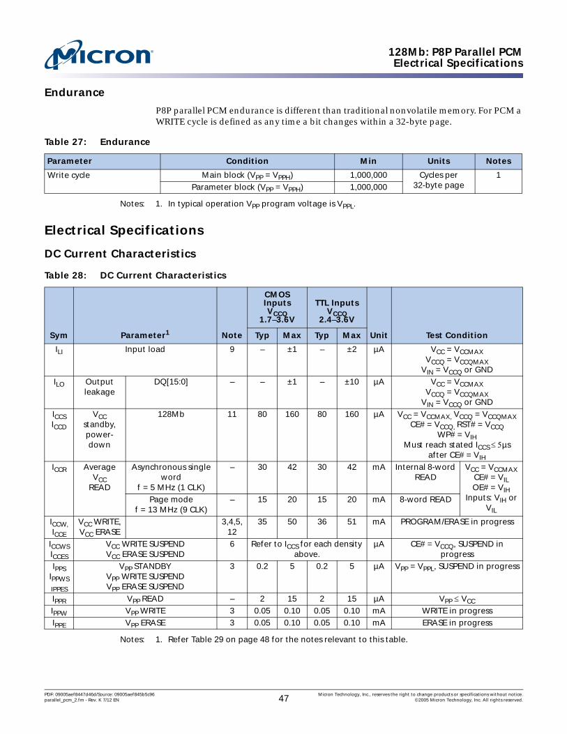
128Mb: P8P Parallel PCMElectrical Specifications
Endurance
P8P parallel PCM endurance is different than traditional nonvolatile memory. For PCM a WRITE cycle is defined as any time a bit changes within a 32-byte page.
Notes: 1. In typical operation VPP program voltage is VPPL.
Electrical Specifications
DC Current Characteristics
Notes: 1. Refer Table 29 on page 48 for the notes relevant to this table.
Table 27: Endurance
Parameter Condition Min Units Notes
Write cycle Main block (VPP = VPPH) 1,000,000 Cycles per32-byte page
1Parameter block (VPP = VPPH) 1,000,000
Table 28: DC Current Characteristics
Sym Parameter1 Note
CMOS InputsVCCQ
1.7–3.6V
TTL InputsVCCQ
2.4–3.6V
Unit Test ConditionTyp Max Typ Max
ILI Input load 9 – ±1 – ±2 µA VCC = VCCMAXVCCQ = VCCQMAX
VIN = VCCQ or GNDILO Output
leakageDQ[15:0] – – ±1 – ±10 µA VCC = VCCMAX
VCCQ = VCCQMAX VIN = VCCQ or GND
ICCS ICCD
VCC standby, power-down
128Mb 11 80 160 80 160 µA VCC = VCCMAX, VCCQ = VCCQMAXCE# = VCCQ, RST# = VCCQ
WP# = VIHMust reach stated ICCS µs
after CE# = VIH
ICCR AverageVCC
READ
Asynchronous single word
f = 5 MHz (1 CLK)
– 30 42 30 42 mA Internal 8-word READ
VCC = VCCMAXCE# = VILOE# = VIH
Inputs: VIH or VIL
Page modef = 13 MHz (9 CLK)
– 15 20 15 20 mA 8-word READ
ICCW, ICCE
VCC WRITE,VCC ERASE
3,4,5, 12
35 50 36 51 mA PROGRAM/ERASE in progress
ICCWS ICCES
VCC WRITE SUSPENDVCC ERASE SUSPEND
6 Refer to ICCS for each density above.
µA CE# = VCCQ, SUSPEND in progress
IPPSIPPWS
IPPES
VPP STANDBYVPP WRITE SUSPENDVPP ERASE SUSPEND
3 0.2 5 0.2 5 µA VPP = VPPL, SUSPEND in progress
IPPR VPP READ – 2 15 2 15 µA VPP VCC
IPPW VPP WRITE 3 0.05 0.10 0.05 0.10 mA WRITE in progressIPPE VPP ERASE 3 0.05 0.10 0.05 0.10 mA ERASE in progress
PDF: 09005aef8447d46d/Source: 09005aef845b5c96 Micron Technology, Inc., reserves the right to change products or specifications without notice.parallel_pcm_2.fm - Rev. K 7/12 EN 47 ©2005 Micron Technology, Inc. All rights reserved.
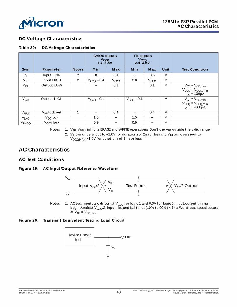
128Mb: P8P Parallel PCMAC Characteristics
DC Voltage Characteristics
Notes: 1. VPP; VPPLK inhibits ERASE and WRITE operations. Don’t use VPP outside the valid range. 2. VIL can undershoot to –1.0V for durations of 2ns or less and VIH can overshoot to
VCCQ(MAX)+1.0V for durations of 2 ns or less.
AC Characteristics
AC Test Conditions
Figure 19: AC Input/Output Reference Waveform
Notes: 1. AC test inputs are driven at VCCQ for logic 1 and 0.0V for logic 0. Input/output timing begins/ends at VCCQ/2. Input rise and fall times (10% to 90%) < 5ns. Worst-case speed occurs at VCC = VCC,min.
Figure 20: Transient Equivalent Testing Load Circuit
Table 29: DC Voltage Characteristics
Sym Parameter Notes
CMOS InputsVCCQ
1.7–3.6V
TTL InputsVCCQ
2.4–3.6V
Unit Test ConditionMin Max Min Max
VIL Input LOW 2 0 0.4 0 0.6 VVIH Input HIGH 2 VCCQ – 0.4 VCCQ 2.0 VCCQ VVOL Output LOW – 0.1 0.1 V VCC = VCC,min
VCCQ = VCCQ,minIOL = 100µA
VOH Output HIGH VCCQ – 0.1 – VCCQ – 0.1 – V VCC = VCC,minVCCQ = VCCQ,min
IOH = –100µAVPPLK VPP lock out 1 – 0.4 – 0.4 VVLKO VCC lock 1.5 – 1.5 – V
VLKOQ VCCQ lock 0.9 – 0.9 – V
Input VCC/2 VCC/2 Output
VCC
0V
Test PointsVIH
VIL
Device undertest
Out
CL
PDF: 09005aef8447d46d/Source: 09005aef845b5c96 Micron Technology, Inc., reserves the right to change products or specifications without notice.parallel_pcm_2.fm - Rev. K 7/12 EN 48 ©2005 Micron Technology, Inc. All rights reserved.

128Mb: P8P Parallel PCMAC Characteristics
Capacitance
Notes: 1. Sampled, not 100% tested.
AC Read Specifications
Notes: 1. See Figure 19 on page 48 for timing measurements and maximum allowable input slew rate.
2. OE# may be delayed by up to tELQV – tGLQV after CE#’s falling edge without impact to tELQV.
3. Sampled, not 100% tested.4. All specs apply to all densities.
Table 30: Test Configuration Component Value for Worst-Case Speed Conditions
Test Configuration CL (pF) (includes jig capacitance)
VCCQ,min 30
Table 31: Capacitance: TA = 25°C, f = 1 MHz1
Symbol Parameter1 Min Typ Max Unit Condition
CIN Input capacitance 2 6 8 pF VIN = 0.0VCOUT Output capacitance 2 4 7 pF VOUT = 0.0V
Table 32: AC Read Specifications
Number Symbol Parameter1
0°C to 70°C –40°C to 85°C
Units NotesMin Max Min Max
R1 tAVAV Read cycle time 115 – 135 – ns 1, 4R2 tAVQV Address to output valid – 115 – 135 ns 1, 4R3 tELQV CE# LOW to output valid – 115 – 135 ns 1, 4R4 tGLQV OE# LOW to output valid – 25 – 25 ns 1, 2, 4R5 tPHQV RST# HIGH to output valid – 150 – 150 ns 1, 4R6 tELQX CE# LOW to output in Low-Z 0 – 0 – ns 3, 4R7 tGLQX OE# LOW to output in Low-Z 0 – 0 – ns 1, 2, 3,
4R8 tEHQZ CE# HIGH to output in High-Z – 24 – 24 ns 1, 3, 4R9 tGHQZ tOE# HIGH to output in High-Z – 24 – 24 ns 1, 3, 4R10 tOH Output hold from first occurring address,
CE#, or OE# change0 – 0 – ns 1, 3, 4
R11 tEHEL CE# pulse width high 20 – 20 – ns 1, 4R108 tAPA Page address access – 25 – 25 ns
PDF: 09005aef8447d46d/Source: 09005aef845b5c96 Micron Technology, Inc., reserves the right to change products or specifications without notice.parallel_pcm_2.fm - Rev. K 7/12 EN 49 ©2005 Micron Technology, Inc. All rights reserved.

128Mb: P8P Parallel PCMAC Characteristics
Figure 21: Asynchronous Single-Word Read
Figure 22: Asynchronous Page Mode Read Timing
AC Write Specifications
Table 33: AC Write Characteristics
Num Sym Parameter1, 2
All Speeds
NotesMin Max Units
W1 tPHWL RST# high recovery to WE# LOW 150 – ns 3W2 tELWL CE# setup to WE# LOW 0 – ns 10W3 tWLWH WE# write pulse width LOW 50 – ns 4W4 tDVWH Data setup to WE# HIGH 50 – nsW5 tAVWH Address valid setup to WE# HIGH 50 – nsW6 tWHEH CE# hold from WE# HIGH 0 – ns 10W7 tWHDX Data hold from WE# HIGH 0 – nsW8 tWHAX Address hold from WE# HIGH 0 – nsW9 tWHWL WE# pulse width HIGH 20 – ns
Address
tAVAV
CE#
OE#
DQ
RST#
tAVQV
tELQV
tGLQV
tGLQXtELQX
tPHQV
tEHQZ
tGHQZ
tOH
tOHtOHtOHtOH
Address
A[3:1]
tAVAV
CE#
OE#
DQ
tAVQV
tELQV
tGLQV
tAPA tAPA tAPAtELQX
Q1 Q2 Q3 Q7
tEHQZ
tGHQZ
PDF: 09005aef8447d46d/Source: 09005aef845b5c96 Micron Technology, Inc., reserves the right to change products or specifications without notice.parallel_pcm_2.fm - Rev. K 7/12 EN 50 ©2005 Micron Technology, Inc. All rights reserved.

128Mb: P8P Parallel PCMAC Characteristics
Notes: 1. Write timing characteristics during ERASE SUSPEND are the same as write-only operations.2. CE#- or WE#-high terminates a WRITE operation.3. Sampled, not 100% tested. 4. Write pulse width low (tWLWH or tELEH) is defined from CE# or WE# LOW (whichever
occurs last) to CE# or WE# HIGH (whichever occurs first). Hence, tWLWH = tELEH = tWLEH = tELWH.
5. Write pulse width HIGH (tWHWL or tEHEL) is defined from CE# or WE# HIGH (whichever is first) to CE# or WE# LOW (whichever is last). Hence, tWHWL = tEHEL = tWHEL = tEHWL.
6. VPP and WP# should be at a valid level without changing state until erase or program suc-cess is determined.
7. This spec is only applicable when transitioning from a WRITE cycle to an asynchronous read. 8. When doing a READ STATUS operation following any command that alters the status regis-
ter contents, W14 is 20ns.9. Add 10ns if the WRITE operation results in a block lock status change, for subsequent READ
operations to reflect this change.10. Guaranteed by design.
Figure 23: Write-to-Write Timing
W10 tVPWH VPP setup to WE# HIGH 200 – ns 3,6W11 tQVVL VPP hold from valid status read 0 – ns 3,6W12 tQVBL WP# hold from valid status read 0 – ns 3,6W13 tBHWH WP# setup to WE# HIGH 200 – ns 3,6W14 tWHGL WE# HIGH to OE# LOW 0 – ns 8W16 tWHQV WE# HIGH to read valid tAVQV+35 – ns 3, 5, 9
Write to Asynchronous Read Specifications
W18 tWHAV WE# HIGH to address valid 0 – ns 3, 5, 7
Table 33: AC Write Characteristics (Continued)
Num Sym Parameter1, 2
All Speeds
NotesMin Max Units
tWHEHtWHEHtELWL tELWL
Address
CE#
WE#
RST#
WP#
OE#
DQ
tWHAVtAVWH
tWHWLtWLWH tWLWH
tWHAVtAVWH
tDVWH tWHDX
tPHWL
tDVWH tWHDX
tBHWH
PDF: 09005aef8447d46d/Source: 09005aef845b5c96 Micron Technology, Inc., reserves the right to change products or specifications without notice.parallel_pcm_2.fm - Rev. K 7/12 EN 51 ©2005 Micron Technology, Inc. All rights reserved.
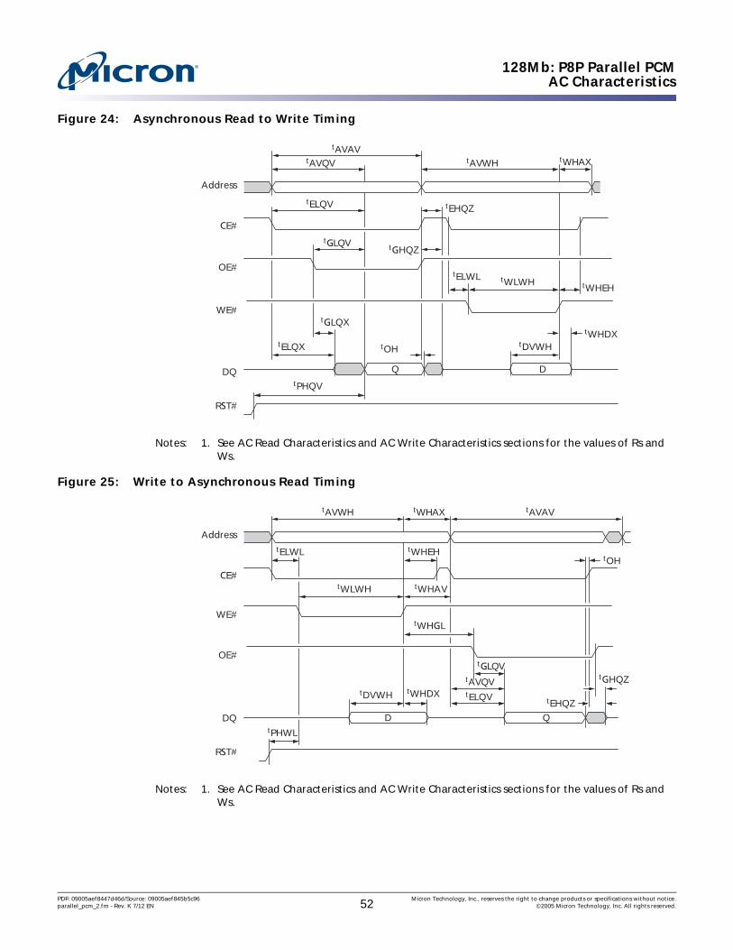
128Mb: P8P Parallel PCMAC Characteristics
Figure 24: Asynchronous Read to Write Timing
Notes: 1. See AC Read Characteristics and AC Write Characteristics sections for the values of Rs and Ws.
Figure 25: Write to Asynchronous Read Timing
Notes: 1. See AC Read Characteristics and AC Write Characteristics sections for the values of Rs and Ws.
tELQV tEHQZ
tGHQZ
tWHEH
tWHDX
tWLWHtELWL
Address
OE#
CE#
RST#
WE#
DQ
tAVAVtAVQV
tGLQV
tWHAXtAVWH
tELQX
tGLQX
tPHQV
tDVWHtOH
Q D
tELQV tEHQZ
tGHQZ
tWHEH
tWHAV
tWHDX
tWHGL
tWLWH
tELWL
Address
WE#
CE#
RST#
OE#
DQ
tAVAV
tAVQV
tGLQV
tWHAXtAVWH
tPHWL
tDVWH
tOH
D Q
PDF: 09005aef8447d46d/Source: 09005aef845b5c96 Micron Technology, Inc., reserves the right to change products or specifications without notice.parallel_pcm_2.fm - Rev. K 7/12 EN 52 ©2005 Micron Technology, Inc. All rights reserved.

128Mb: P8P Parallel PCMAC Characteristics
SPI AC Specifications
Notes: 1. TCH + TCL must be greater than or equal to 1/fC(max).2. Sampled, not 100% tested.3. Expressed as a slew rate.4. Only applicable as a constraint for a WRSR instruction when SRWD is set to 1.
Table 34: SPI AC Specifications
Sym Parameter
Speed All Speeds
UnitsNote Min MaxfC Clock frequency for all instructions except READ (0°C to 70°C) DC 50 MHzfC Clock frequency for all instructions except READ (–40°C to 85°C) DC 33 MHzfR Clock frequency for READ DC 25 MHz
tCH Clock high time 1 9 – nstCL Clock low time 1 9 – ns
tCLCH Clock rise time (peak to peak) 2, 3 0.1 – V/nstCHCL Clock fall time (peak to peak) 2, 3 0.1 – V/nstSLCH S# active setup time (relative to C) 5 – nstCHSL S# active hold time (relative to C) 5 – nstDVCH Data input setup time 2 – nstCHDX Data input hold time 5 – nstCHSH S# active hold time (relative to C) 5 – nstSHCH S# inactive hold time (relative to C) 5 – nstSHSL S# deselect time 100 – nstSHQZ Output disable time 2 – 8 nstCLQV Clock low to output valid – 9 nstCLQX Output hold time 0 – nstHLCH HOLD# assertion setup time (relative to C) 5 – nstCHHH HOLD# assertion hold time (relative to C) 5 – nstHHCH HOLD# de-assertion setup time (relative to C) 5 – nstCHHL HOLD# de-assertion hold time (relative to C) 5 – nstHHQX HOLD# de-assertion to output Low-Z 2 10 nstHLQZ HOLD# de-assertion to output High-Z 2 10 nstWHSL W# setup time 4 20 – nstSHWL W# hold time 4 100 – ns
PDF: 09005aef8447d46d/Source: 09005aef845b5c96 Micron Technology, Inc., reserves the right to change products or specifications without notice.parallel_pcm_2.fm - Rev. K 7/12 EN 53 ©2005 Micron Technology, Inc. All rights reserved.

128Mb: P8P Parallel PCMAC Characteristics
Figure 26: Serial Input Timing
Figure 27: Write Protect Setup and Hold Timing during WRSR when SRWD = 1
Figure 28: Hold Timing
tSLCHtCHSL
tDVCHtCHDX
tCHSH tSHCH
tSHSL
C
S#
DQ0
Q
MSB LSB
High-Z
W#
S#
C
DQ0
DQ1
tWHSL tSHWL
tHLCHtCHHL tHHCH
tHLQZ
tCHHHtHHQX
S#
C
DQ0
DQ1
HOLD#
PDF: 09005aef8447d46d/Source: 09005aef845b5c96 Micron Technology, Inc., reserves the right to change products or specifications without notice.parallel_pcm_2.fm - Rev. K 7/12 EN 54 ©2005 Micron Technology, Inc. All rights reserved.

128Mb: P8P Parallel PCMProgram and Erase Characteristics
Figure 29: Output Timing
Program and Erase Characteristics
Notes: 1. Typical values measured at TA = 25°C, typical voltages and 50% data pattern per word. Excludes system overhead. Performance numbers are valid for all speed versions. Sampled, but not 100% tested.
2. Averaged over entire device.3. W602 is the minimum time between an initial BLOCK ERASE or ERASE RESUME command
and the a subsequent ERASE SUSPEND command. Violating the specification repeatedly during any particular BLOCK ERASE may cause erase failures in Flash devices. This specifica-tion is required if the designer wishes to maintain compatibility with the P33 NOR Flash device. However, it is not required with PCM.
Table 35: Program and Erase Specifications
Operation1 Symbol Parameter Description
VPPL4, 5
UnitMin Typ Max
Erasing and Suspending
Erase to suspend W602 3 tERS/SUSP ERASE or ERASE RESUME command to ERASE SUSPEND command
– 500 – µs
Erase time W500 tERS/PB 16KW parameter – 100 200 msW501 tERS/MB 64KW main – 400 800
Suspend latency W600 tSUSP/P Write suspend – 35 60 µsW601 tSUSP/E Erase suspend – 35 60
Conventional Word Programming
Program time6 W200 tPROG/W Single word – 60 120 µs
Buffered Programming
Program time W200 tPROG/W Single word(legacy program and bit-
alterable write)
5 120 240 µs
W250 tPROG/PB One buffer (64 bytes/32 words)
(legacy program and bit-alterable write)
4,5 120 360 µs
One buffer (64 bytes/32 words)
(program on all 1s)
71 280
tCL tCH
S#
C
DQ0
DQ1
LSB out
AddressLSB in
tCLQX tCLQX tSHQZ
tCLQV tCLQV
PDF: 09005aef8447d46d/Source: 09005aef845b5c96 Micron Technology, Inc., reserves the right to change products or specifications without notice.parallel_pcm_2.fm - Rev. K 7/12 EN 55 ©2005 Micron Technology, Inc. All rights reserved.
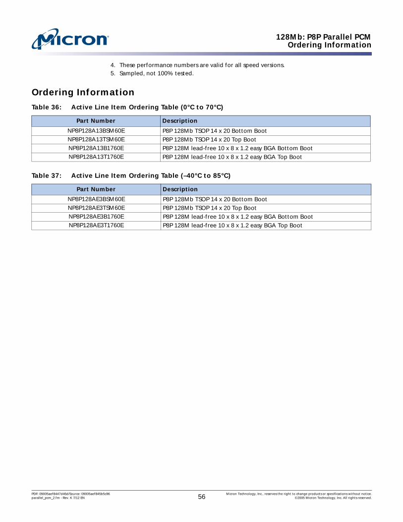
128Mb: P8P Parallel PCMOrdering Information
4. These performance numbers are valid for all speed versions.5. Sampled, not 100% tested.
Ordering Information
Table 36: Active Line Item Ordering Table (0°C to 70°C)
Part Number Description
NP8P128A13BSM60E P8P 128Mb TSOP 14 x 20 Bottom Boot NP8P128A13TSM60E P8P 128Mb TSOP 14 x 20 Top Boot NP8P128A13B1760E P8P 128M lead-free 10 x 8 x 1.2 easy BGA Bottom Boot NP8P128A13T1760E P8P 128M lead-free 10 x 8 x 1.2 easy BGA Top Boot
Table 37: Active Line Item Ordering Table (–40°C to 85°C)
Part Number Description
NP8P128AE3BSM60E P8P 128Mb TSOP 14 x 20 Bottom Boot NP8P128AE3TSM60E P8P 128Mb TSOP 14 x 20 Top Boot NP8P128AE3B1760E P8P 128M lead-free 10 x 8 x 1.2 easy BGA Bottom Boot NP8P128AE3T1760E P8P 128M lead-free 10 x 8 x 1.2 easy BGA Top Boot
PDF: 09005aef8447d46d/Source: 09005aef845b5c96 Micron Technology, Inc., reserves the right to change products or specifications without notice.parallel_pcm_2.fm - Rev. K 7/12 EN 56 ©2005 Micron Technology, Inc. All rights reserved.

128Mb: P8P Parallel PCMSupplemental Reference Information
Supplemental Reference Information
Flowcharts
Figure 30: WORD PROGRAM or BIT-ALTERABLE WORD WRITE Flowchart
Notes: 1. Repeat for subsequent WRITE operations2. Full status register check can be done after each WRITE or after a sequence of WRITE opera-
tions.
Table 38: WORD PROGRAM or BIT-ALTERABLE WORD WRITE Procedure
Bus Operation Command Notes
WRITE PROGRAM/WRITE SETUP
Data = 40h or 42h (bit alterableAddr = Location to WRITE (WA)
WRITE DATA Data = Data to be written (WD)Addr = Location to be written (WA)
READ Status register data; initiate a READ cycle to update status registerStandby Check SR7
1 = WSM ready0 = WSM busy
0
Writecomplete
1
SR7 =
Write 40h or 42h word address
Start
Write dataword address
Programsetup
Confirmdata
Read statusregister
Suspend writeloop
Yes
No
Suspendwrite
Full status check(if desired)
PDF: 09005aef8447d46d/Source: 09005aef845b5c96 Micron Technology, Inc., reserves the right to change products or specifications without notice.parallel_pcm_2.fm - Rev. K 7/12 EN 57 ©2005 Micron Technology, Inc. All rights reserved.
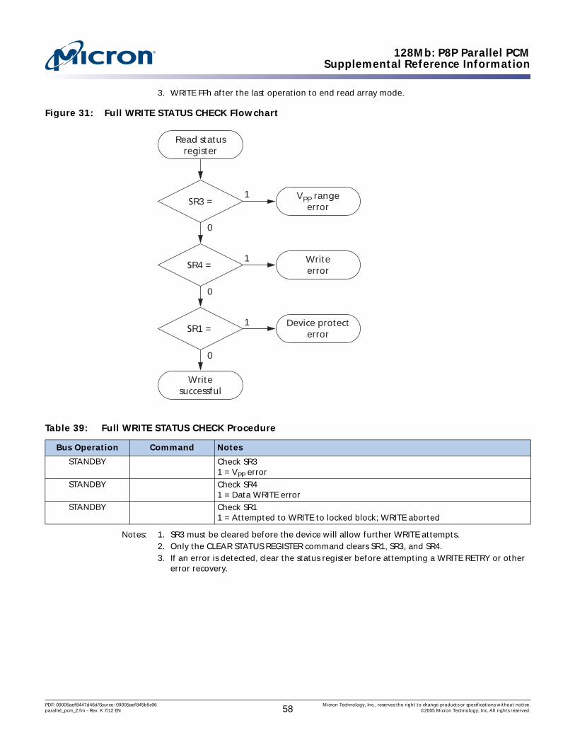
128Mb: P8P Parallel PCMSupplemental Reference Information
3. WRITE FFh after the last operation to end read array mode.
Figure 31: Full WRITE STATUS CHECK Flowchart
Notes: 1. SR3 must be cleared before the device will allow further WRITE attempts.2. Only the CLEAR STATUS REGISTER command clears SR1, SR3, and SR4.3. If an error is detected, clear the status register before attempting a WRITE RETRY or other
error recovery.
Table 39: Full WRITE STATUS CHECK Procedure
Bus Operation Command Notes
STANDBY Check SR31 = VPP error
STANDBY Check SR41 = Data WRITE error
STANDBY Check SR11 = Attempted to WRITE to locked block; WRITE aborted
Writesuccessful
1
0
1
0
1
0
Read statusregister
SR3 =
SR4 =
SR1 =
Writeerror
Device protecterror
VPP rangeerror
PDF: 09005aef8447d46d/Source: 09005aef845b5c96 Micron Technology, Inc., reserves the right to change products or specifications without notice.parallel_pcm_2.fm - Rev. K 7/12 EN 58 ©2005 Micron Technology, Inc. All rights reserved.

128Mb: P8P Parallel PCMSupplemental Reference Information
Figure 32: WRITE SUSPEND/RESUME Flowchart
0
1
SR7 =
Write 70hs
Start
Write B0hany address
Programsuspend
Readstatus
Write FFh Read array
Writeresume
Write D0hany address
Read arraydata
Write FFh Read array
Read arraydata
Read statusregister
0
1
SR2 =
Writeresumed
No
Yes
Donereading?
Writecompleted
PDF: 09005aef8447d46d/Source: 09005aef845b5c96 Micron Technology, Inc., reserves the right to change products or specifications without notice.parallel_pcm_2.fm - Rev. K 7/12 EN 59 ©2005 Micron Technology, Inc. All rights reserved.

128Mb: P8P Parallel PCMSupplemental Reference Information
Table 40: WRITE SUSPEND/RESUME Procedure
Bus Operation Command Notes
WRITE READ STATUS Data = 70hAddr = Block to suspend (BA)
WRITE WRITE SUSPEND Data = B0hAddr = X
READ Status register data; initiate a READ cycle to update status registerAddr = Suspended block (BA)
STANDBY Check SR71 = WSM ready0 = WSM busy
STANDBY Check SR21 = Program suspended0 = Program completed
WRITE READ ARRAY Data = FFhAddr = Block address to be read (BA)
READ Read array data from block other than the one being writtenWRITE WRITE RESUME Data = D0h
Addr = Suspended block (BA)
PDF: 09005aef8447d46d/Source: 09005aef845b5c96 Micron Technology, Inc., reserves the right to change products or specifications without notice.parallel_pcm_2.fm - Rev. K 7/12 EN 60 ©2005 Micron Technology, Inc. All rights reserved.
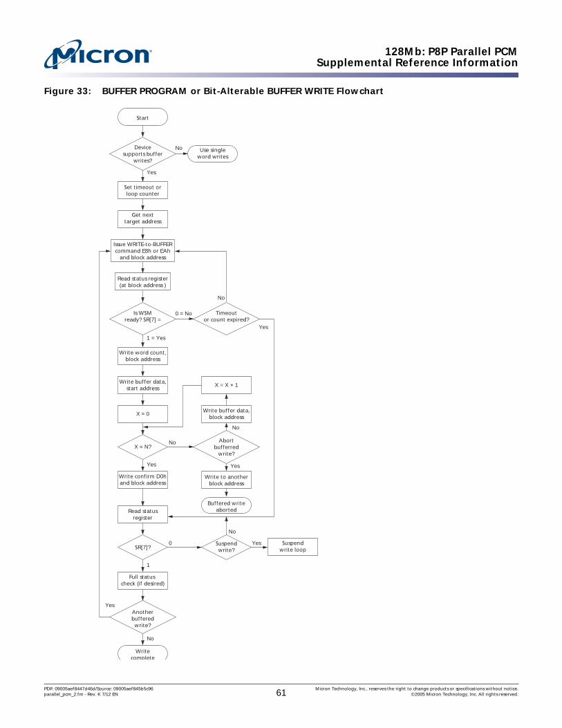
128Mb: P8P Parallel PCMSupplemental Reference Information
Figure 33: BUFFER PROGRAM or Bit-Alterable BUFFER WRITE Flowchart
Yes
Is WSMready? SR[7] =
Set timeout orloop counter
Start
Use singleword writes
Get nexttarget address
Read status register(at block address )
Timeoutor count expired?
Issue WRITE-to-BUFFERcommand E8h or EAh
and block address
X = 0
Write confirm D0hand block address
Read statusregister
Devicesupports buffer
writes?
Write word count,block address
Write buffer data,start address
Write buffer data,block address
X = X + 1
No
No
0 = No
No
Yes
Yes
1 = Yes
No
Yes
X = N?Abort
bufferredwrite?
0 Yes
No
Full status check (if desired)
1
SR[7]?Suspendwrite?
No
Anotherbuffered
write?
Writecomplete
Write to anotherblock address
Suspendwrite loop
Buffered writeaborted
Yes
PDF: 09005aef8447d46d/Source: 09005aef845b5c96 Micron Technology, Inc., reserves the right to change products or specifications without notice.parallel_pcm_2.fm - Rev. K 7/12 EN 61 ©2005 Micron Technology, Inc. All rights reserved.
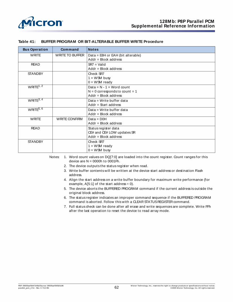
128Mb: P8P Parallel PCMSupplemental Reference Information
Notes: 1. Word count values on DQ[7:0] are loaded into the count register. Count ranges for this device are N = 0000h to 0001Fh.
2. The device outputs the status register when read.3. Write buffer contents will be written at the device start address or destination Flash
address.4. Align the start address on a write buffer boundary for maximum write performance (for
example, A[5:1] of the start address = 0).5. The device aborts the BUFFERED PROGRAM command if the current address is outside the
original block address.6. The status register indicates an improper command sequence if the BUFFERED PROGRAM
command is aborted. Follow this with a CLEAR STATUS REGISTER command.7. Full status check can be done after all erase and write sequences are complete. Write FFh
after the last operation to reset the device to read array mode.
Table 41: BUFFER PROGRAM OR BIT-ALTERABLE BUFFER WRITE Procedure
Bus Operation Command Notes
WRITE WRITE TO BUFFER Data = E8H or EAH (bit alterable)Addr = Block address
READ SR7 = ValidAddr = Block address
STANDBY Check SR71 = WSM busy0 = WSM ready
WRITE1, 2 Data = N - 1 = Word countN = 0 corresponds to count = 1Addr = Block address
WRITE3, 4 Data = Write buffer dataAddr = Start address
WRITE5, 6 Data = Write buffer dataAddr = Block address
WRITE WRITE CONFIRM Data = D0HAddr = Block address
READ Status register dataCE# and CE# LOW updates SRAddr = Block address
STANDBY Check SR71 = WSM ready0 = WSM busy
PDF: 09005aef8447d46d/Source: 09005aef845b5c96 Micron Technology, Inc., reserves the right to change products or specifications without notice.parallel_pcm_2.fm - Rev. K 7/12 EN 62 ©2005 Micron Technology, Inc. All rights reserved.

128Mb: P8P Parallel PCMSupplemental Reference Information
Figure 34: BLOCK ERASE Flowchart
Notes: 1. Repeat for subsequent block erasures2. Full status register check can be done after each block erase or after a sequence of block
erasures.3. Write FFh after the last operation to enter read array mode.
Table 42: BLOCK ERASE Procedure
Bus Operation Command Notes
WRITE BLOCK ERASE SETUP
Data = 20hAddr = Block to be erased (BA)
WRITE ERASE CONFIRM Data = D0hAddr = Block to be erased (BA)
READ Status register data; toddle CE# or OE# to update status register dataSTANDBY Check SR7
1 = WSM ready0 = WSM busy
0
Block erasecomplete
1
SR7 =
Write 20hblock address
Start
Write dataword address
Block erase
Erase confirm
Read statusregister
Suspend eraseloop
Yes
No
Suspenderase
Full status check(if desired)
PDF: 09005aef8447d46d/Source: 09005aef845b5c96 Micron Technology, Inc., reserves the right to change products or specifications without notice.parallel_pcm_2.fm - Rev. K 7/12 EN 63 ©2005 Micron Technology, Inc. All rights reserved.

128Mb: P8P Parallel PCMSupplemental Reference Information
Figure 35: BLOCK ERASE FULL ERASE STATUS CHECK Flowchart
Notes: 1. Only the CLEAR STATUS REGISTER command clears SR1, SR3, SR4, and SR5.2. If an error is detected, clear the status register before attempting an erase retry or other
error recovery.
Table 43: BLOCK ERASE FULL ERASE STATUS CHECK Procedure
Bus Operation Command Notes
STANDBY Check SR31 = VPP error
STANDBY Check SR4, SR51 = Command sequence error
STANDBY Check SR51 = Block erase error
STANDBY Check SR11 = Attempted erase of locked block erase aborted
1
0
1
0
1
Read statusregister
SR3 =
SR4, 5 =
SR5 =
Commandsequence error
Block eraseerror
Block erasesuccessful
0
1
0
SR1 = Erase of lockedblock aborted
VPP rangeerror
PDF: 09005aef8447d46d/Source: 09005aef845b5c96 Micron Technology, Inc., reserves the right to change products or specifications without notice.parallel_pcm_2.fm - Rev. K 7/12 EN 64 ©2005 Micron Technology, Inc. All rights reserved.

128Mb: P8P Parallel PCMSupplemental Reference Information
Figure 36: ERASE SUSPEND/RESUME Flowchart
0
1
SR7 =
Write 70hany address
Start
Write B0hany address
Erasesuspend
Read status
ProgramRead
(Erase resume)
Read status
Write D0hany address
Programloop
Read arraydata
Write 70hany address
Write FFhany address Read array
Read arraydata
Read statusregister
0
1
SR6 =
Eraseresumed
No
Yes
Done?
Read orprogram?
Erasecompleted
PDF: 09005aef8447d46d/Source: 09005aef845b5c96 Micron Technology, Inc., reserves the right to change products or specifications without notice.parallel_pcm_2.fm - Rev. K 7/12 EN 65 ©2005 Micron Technology, Inc. All rights reserved.

128Mb: P8P Parallel PCMSupplemental Reference Information
Table 44: ERASE SUSPEND/RESUME Procedure
Bus Operation Command Notes
WRITE READ STATUS Data = 70hAddr = Any device address
WRITE ERASE SUSPEND Data = B0hAddr = Same partition address as above
READ Status register data; toggle CE# or OE# to update status registerAddr = X
STANDBY Check SR71 = WSM ready0 = WSM busy
STANDBY Check SR1 = Erase suspended0 = Erase completed
WRITE READ ARRAY OR PROGRAM
Data = FFh or 40hAddr = Block to program or read
READ or WRITE Read array or program data from/to block other than the one being erasedWRITE PROGRAM RESUME Data = D0h
Addr = Any address
PDF: 09005aef8447d46d/Source: 09005aef845b5c96 Micron Technology, Inc., reserves the right to change products or specifications without notice.parallel_pcm_2.fm - Rev. K 7/12 EN 66 ©2005 Micron Technology, Inc. All rights reserved.

128Mb: P8P Parallel PCMSupplemental Reference Information
Figure 37: LOCKING OPERATIONS Flowchart
Table 45: LOCKING OPERATIONS Procedure
Bus Operation Command Notes
WRITE LOCK SETUP Data = 60hAddr = Block to lock/unlock/lock-down (BA)
WRITE LOCK, UNLOCK, OR LOCKDOWN
CONFIRM
Data = 01h (Lock block)D0h (Unlock block)2Fh (Lock-down block)Addr = Block to lock/unlock/lock-down (BA)
WRITE (optional) READ ID PLANE Data = 90hAddr = Block address offset + 2 (BA + 2)
READ (optional) BLOCK LOCK STATUS
Block lock status dataAddr = Block address offset + 2 (BA + 2)
No
Yes
Lockingchange?
Write 60hblock address
Start
Write 01h/D0h/2Fhblock address
Lock confirm
Read ID plane
Lock setup
Read array
Op
tio
nal
Write FFhany address
Write 0x90
Read blocklock status
Lock changecomplete
PDF: 09005aef8447d46d/Source: 09005aef845b5c96 Micron Technology, Inc., reserves the right to change products or specifications without notice.parallel_pcm_2.fm - Rev. K 7/12 EN 67 ©2005 Micron Technology, Inc. All rights reserved.

128Mb: P8P Parallel PCMSupplemental Reference Information
Figure 38: PROGRAM PROTECTION REGISTER Flowchart
STANDBY (optional)
Confirm locking change on DQ1, DQ0 (see Table 14 on page 26 for valid combinations)
WRITE READ ARRAY Data = FFhAddr = Block address (BA)
Table 46: PROGRAM PROTECTION REGISTER Procedure
Bus Operation Command Notes
WRITE PROGRAM PR SETUP
Data = 0xC0Addr = First location to program
WRITE PROTECTION PROGRAM
Data = Data to programAddr = Location to program
READ None Status register dataIDLE None Check SR7
1 = WSM ready0 = WSM busy
Table 45: LOCKING OPERATIONS Procedure (Continued)
Bus Operation Command Notes
0
Programcomplete
1
SR7 =
Write 0xC0, PR address
Start
Write PRaddress and data
Programsetup
Confirmdata
Read statusregister
Full status check(if desired)
PDF: 09005aef8447d46d/Source: 09005aef845b5c96 Micron Technology, Inc., reserves the right to change products or specifications without notice.parallel_pcm_2.fm - Rev. K 7/12 EN 68 ©2005 Micron Technology, Inc. All rights reserved.

128Mb: P8P Parallel PCMSupplemental Reference Information
Notes: 1. PROGRAM PROTECTION REGISTER operation addresses must be within the protection regis-ter address space. Addresses outside this space will return an error.
2. Repeat for subsequent programming operations.3. Full status register check can be done after each program or after a sequence of PROGRAM
operations.4. Write 0xFF after the last operation to set read array state.
Figure 39: FULL STATUS CHECK Flowchart
Notes: 1. Only the CLEAR STATUS REGISTER command clears SR1, SR3, and SR4.2. If an error is detected, clear the status register before attempting a program retry or other
error recovery.
Table 47: FULL STATUS CHECK Procedure
Bus Operation Command Notes
IDLE None Check SR31 = VPP range error
IDLE None Check SR41 = Programming error
IDLE None Check SR11 = Block locked; operation aborted
Programsuccessful
1
0
1
0
1
0
Read statusregister
SR3 =
SR4 =
SR1 =
Programerror
Register locked;program aborted
VPP rangeerror
PDF: 09005aef8447d46d/Source: 09005aef845b5c96 Micron Technology, Inc., reserves the right to change products or specifications without notice.parallel_pcm_2.fm - Rev. K 7/12 EN 69 ©2005 Micron Technology, Inc. All rights reserved.
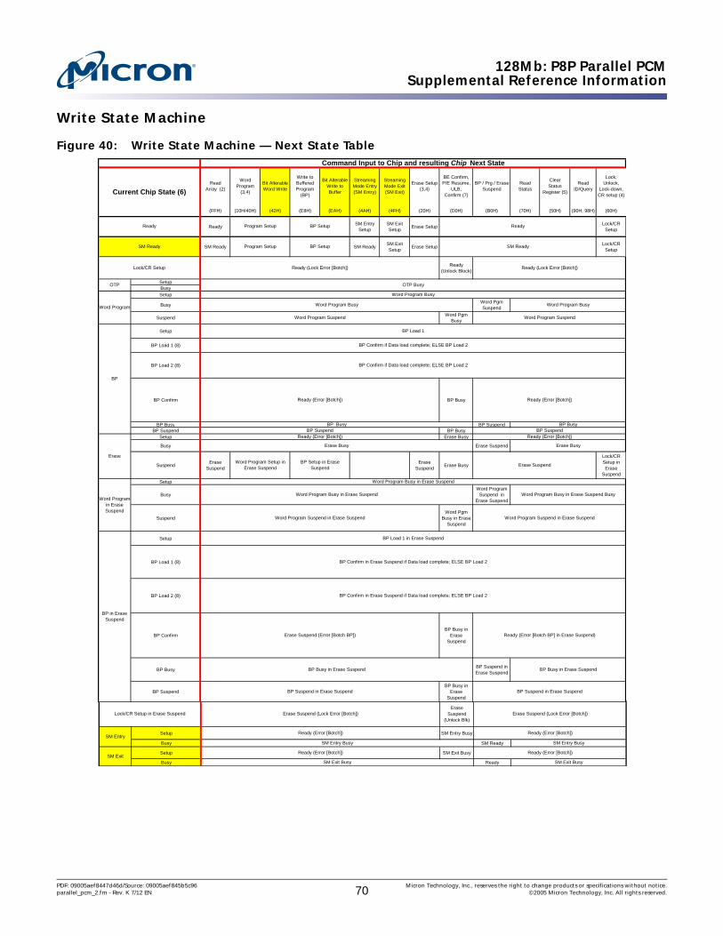
128Mb: P8P Parallel PCMSupplemental Reference Information
Write State Machine
Figure 40: Write State Machine — Next State Table
Erase Suspend
(Unlock Blk)
Setup SM Entry Busy
Busy SM Ready
Setup SM Exit Busy
Busy Ready
SM EntrySM Entry Busy SM Entry Busy
Ready (Error [Botch]) Ready (Error [Botch])
SM ExitSM Exit Busy SM Exit Busy
Ready (Error [Botch])
Erase Suspend (Lock Error [Botch])Erase Suspend (Lock Error [Botch])Lock/CR Setup in Erase Suspend
Ready (Error [Botch])
Read Array (2)
Word Program
(3,4)
Bit Alterable Word Write
Write to Buffered Program
(BP)
Bit Alterable Write to Buffer
Streaming Mode Entry (SM Entry)
Streaming Mode Exit (SM Exit)
Erase Setup (3,4)
BE Confirm,P/E Resume,
ULB,Confirm (7)
BP / Prg / Erase Suspend
ReadStatus
Clear Status
Register (5)
Read ID/Query
Lock, Unlock,
Lock-down, CR setup (4)
(FFH) (10H/40H) (42H) (E8H) (EAH) (4AH) (4FH) (20H) (D0H) (B0H) (70H) (50H) (90H, 98H) (60H)
ReadySM Entry
SetupSM Exit Setup
Erase SetupLock/CR
Setup
SM Ready SM ReadySM Exit Setup
Erase SetupLock/CR
Setup
Ready (Unlock Block)
SetupBusySetup
BusyWord Pgm Suspend
SuspendWord Pgm
Busy
Setup
BP Load 1 (8)
BP Load 2 (8)
BP Confirm BP Busy
BP Busy BP Suspend BP Suspend BP Busy
Setup Erase Busy
Busy Erase Suspend
SuspendErase
SuspendErase
SuspendErase Busy
Lock/CR Setup in Erase
Suspend
Setup
BusyWord Program
Suspend in Erase Suspend
SuspendWord Pgm
Busy in Erase Suspend
Setup
BP Load 1 (8)
BP Load 2 (8)
BP ConfirmBP Busy in
Erase Suspend
BP BusyBP Suspend in Erase Suspend
BP SuspendBP Busy in
Erase Suspend
Ready Program Setup BP Setup Ready
Word Program Busy
BP Confirm if Data load complete; ELSE BP Load 2
BP Confirm if Data load complete; ELSE BP Load 2
Word Program SuspendWord Program Suspend
Ready (Error [Botch BP] in Erase Suspend)Erase Suspend (Error [Botch BP])
Erase Suspend
BP Confirm in Erase Suspend if Data load complete; ELSE BP Load 2
Command Input to Chip and resulting Chip Next State
Erase Busy
BP SuspendBP Busy BP Busy
Word Program Busy
OTP Busy
Ready (Lock Error [Botch])
BP SetupProgram Setup
Word Program Busy in Erase Suspend
Erase Busy
BP Busy in Erase Suspend BP Busy in Erase Suspend
Word Program Busy in Erase Suspend
Word Program Busy
Word Program Setup in Erase Suspend
BP Setup in Erase Suspend
BP Suspend in Erase Suspend BP Suspend in Erase Suspend
Word Program Suspend in Erase Suspend
BP Suspend
BP in Erase Suspend
BP
Ready (Error [Botch]) Ready (Error [Botch])
Ready (Error [Botch]) Ready (Error [Botch])
Lock/CR Setup
OTP
SM Ready SM Ready
Ready (Lock Error [Botch])
Erase
Word Program in Erase Suspend
BP Confirm in Erase Suspend if Data load complete; ELSE BP Load 2
BP Load 1 in Erase Suspend
BP Load 1
Word Program Suspend in Erase Suspend
Word Program Busy in Erase Suspend Busy
Current Chip State (6)
Word Program
PDF: 09005aef8447d46d/Source: 09005aef845b5c96 Micron Technology, Inc., reserves the right to change products or specifications without notice.parallel_pcm_2.fm - Rev. K 7/12 EN 70 ©2005 Micron Technology, Inc. All rights reserved.
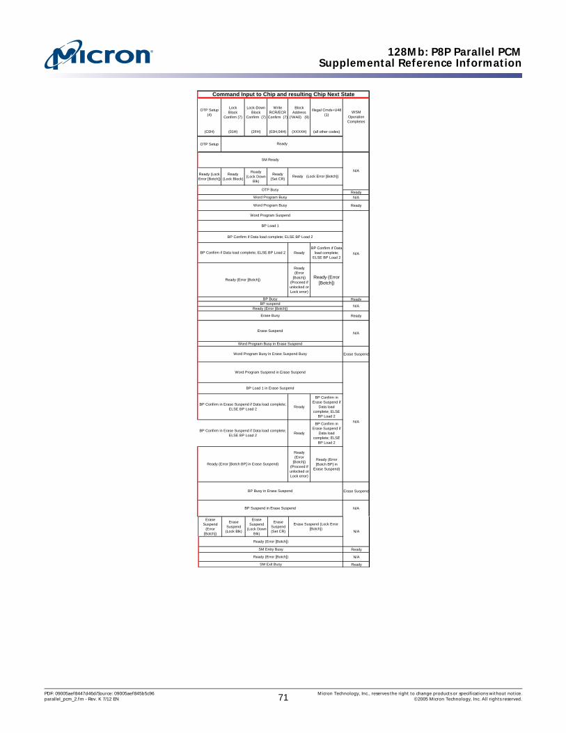
128Mb: P8P Parallel PCMSupplemental Reference Information
OTP Setup (4)
LockBlock
Confirm (7)
Lock-Down Block
Confirm (7)
Write RCR/ECR
Confirm (7)
Block Address
(¹WA0) (9)
Illegal Cmds+U48 (1)
(C0H) (01H) (2FH) (03H,04H) (XXXXH) (all other codes)
OTP Setup
Ready (Lock Error [Botch])
Ready (Lock Block)
Ready (Lock Down
Blk)
Ready (Set CR)
ReadyN/A
Ready
ReadyBP Confirm if Data
load complete; ELSE BP Load 2
Ready (Error
[Botch]) (Proceed if unlocked or Lock error)
Ready (Error [Botch])
Ready
Ready
Erase Suspend
Ready
BP Confirm in Erase Suspend if
Data load complete; ELSE
BP Load 2
Ready
BP Confirm in Erase Suspend if
Data load complete; ELSE
BP Load 2
Ready (Error
[Botch]) (Proceed if unlocked or Lock error)
Ready (Error [Botch BP] in
Erase Suspend)
Erase Suspend
N/A
Ready
SM Ready
Word Program Busy
N/A
BP Suspend in Erase Suspend
BP Busy in Erase Suspend
Word Program Suspend in Erase Suspend
BP Load 1 in Erase Suspend
BP Confirm in Erase Suspend if Data load complete; ELSE BP Load 2
N/A
BP Confirm in Erase Suspend if Data load complete; ELSE BP Load 2
Ready (Error [Botch BP] in Erase Suspend)
Ready (Error [Botch])
BP Confirm if Data load complete; ELSE BP Load 2 N/A
N/A
BP Busy
Ready (Error [Botch])
BP Confirm if Data load complete; ELSE BP Load 2
BP suspend
BP Load 1
Word Program Busy in Erase Suspend
Word Program Busy in Erase Suspend Busy
Erase Suspend
Erase Busy
N/A
OTP Busy
Ready (Lock Error [Botch])
WSM Operation Completes
Command Input to Chip and resulting Chip Next State
Word Program Busy
Word Program Suspend
Erase Suspend
(Error [Botch])
Erase Suspend (Lock Blk)
Erase Suspend
(Lock Down Blk)
Erase Suspend (Set CR)
Ready
N/A
Ready
N/A
Ready (Error [Botch])
SM Entry Busy
Ready (Error [Botch])
SM Exit Busy
Erase Suspend (Lock Error [Botch])
PDF: 09005aef8447d46d/Source: 09005aef845b5c96 Micron Technology, Inc., reserves the right to change products or specifications without notice.parallel_pcm_2.fm - Rev. K 7/12 EN 71 ©2005 Micron Technology, Inc. All rights reserved.

128Mb: P8P Parallel PCMSupplemental Reference Information
Notes: 1. Illegal commands include commands outside of the allowed command set (allowed com-mands: 40H [pgm], 20H [erase]).
2. If a READ ARRAY is attempted while the device is busy writing or erasing, the result will be invalid data. The ID and query data are located at different locations in the address map.
3. First and second cycles of two cycles WRITE commands must be given to the same device address, or unexpected results will occur.
4. The second cycle of the following two cycle commands will be ignored by the user interface: word program setup, erase setup, OTP setup, and lock/unlock/lock down/CR setup when issued in an illegal condition. Illegal conditions are such as "pgm setup while busy", “erase setup while busy", “Word program suspend”, etc. For example, the second cycle of an ERASE command issued in PROGRAM SUSPEND will NOT resume the program operation.
5. The CLEAR STATUS COMMAND only clears the error bits in the status register if the device is not in the following modes: 1. WSM running (Pgm Busy, Erase Busy, Pgm Busy In Erase Sus-pend, OTP Busy, modes); 2. Suspend states (Pgm Suspend, Pgm Suspend In Erase Suspend)
Read Array (2)
Word Program
Setup (3,4)
Bit Alterable Word Write
Write to Buffered Program
(BP)
Bit Alterable Write to Buffer
Streaming Mode Entry (SM Entry)
Streaming Mode Exit (SM Exit)
Erase Setup (3,4)
BE Confirm, P/E Resume, ULB Confirm
(7)
Program/Erase
Suspend
ReadStatus
Clear Status
Register (5)
Read ID/Query
Lock, Unlock,
Lock-down, CR setup (4)
(FFH) (10H/40H) (42H) (E8H) (EAH) (4AH) (4FH) (20H) (D0H) (B0H) (70H) (50H) (90H, 98H) (60H)
Status Read
BP Busy,Word Program Busy,Erase Busy,BP BusyBP Busy in Erase SuspendWord Pgm Suspend,Word Pgm Busy in Erase Suspend,Pgm Suspend In Erase SuspendBP Suspend in Erase SuspendSM Entry BusySM Exit Busy
Ready, SM ReadyErase Suspend, BP Suspend
Lock/CR Setup, Lock/CR Setup in Erase Susp
Erase Setup, OTP Setup, BP: Setup, Load 1, Load 2, Confirm, Word Pgm Setup, SM Entry Setup, SM Exit Setup
Read Array Status ReadReady Array
ID Read
Status Read
Status Read
OTP Busy
Current chip state
Command Input to Chip and resulting Output Mux Next State
Status Read Output mux does not change.
OTP Setup (4)
LockBlock
Confirm (7)
Lock-Down Block
Confirm (7)
Write RCR/ECR
Confirm (7)
Block Address (WA0)
Illegal Cmds (1)
(C0H) (01H) (2FH) (03H,04H) (FFFFH) (all other codes)
Command Input to Chip and resulting Output Mux Next State
Status Read
Current chip state
BP Busy,Word Program Busy,Erase Busy,BP BusyBP Busy in Erase SuspendWord Pgm Suspend,Word Pgm Busy in Erase Suspend,Pgm Suspend In Erase SuspendBP Suspend in Erase SuspendSM Entry BusySM Exit Busy
Ready, SM ReadyErase Suspend, BP Suspend
Erase Setup, OTP Setup, BP: Setup, Load 1, Load 2, Confirm, Word Pgm Setup, SM Entry Setup, SM Exit Setup
Lock/CR Setup, Lock/CR Setup in Erase Susp
OTP Busy
Status Read
Read ArrayStatus Read Output mux does not change. Ready Array
Status ReadReady Array
WSM Operation Completes
PDF: 09005aef8447d46d/Source: 09005aef845b5c96 Micron Technology, Inc., reserves the right to change products or specifications without notice.parallel_pcm_2.fm - Rev. K 7/12 EN 72 ©2005 Micron Technology, Inc. All rights reserved.

128Mb: P8P Parallel PCMSupplemental Reference Information
6. The current state is that of the device.7. Confirm commands (LOCK BLOCK, UNLOCK BLOCK, LOCK DOWN BLOCK) perform the oper-
ation and then move to the ready state.8. Buffered programming will botch when a different block address (as compared to address
given with E8 command) is written during the BP load1 and BP load2 states.9. WA0 refers to the block address latched during the first WRITE cycle of the current opera-
tion.
Common Flash Interface
The P8P parallel PCM device borrows from the existing standards established for Flash memory and supports the use of the CFI. The query is part of an overall specification for multiple command set and control interface descriptions called CFI. This appendix defines the data structure or database returned by the CFI QUERY command. System software should parse this structure to gain critical information, such as block size, density, x16, and electrical specifications. After this information has been obtained, the software will know which command sets to use to enable PCM writes, block erases, and otherwise control the PCM component.
Query Structure Output
The query database allows system software to obtain information for controlling the PCM device. This section describes the device’s CFI-compliant interface that allows access to query data.
Query data are presented on the lowest-order data outputs (DQ[7:0]) only. The numer-ical offset value is the address relative to the maximum bus width supported by the device. On this family of devices, the query table device starting address is a 10h, which is a word address for x16 devices.
For a word-wide (x16) device, the first two query-structure bytes, ASCII “Q” and “R,” appear on the low byte at word addresses 10h and 11h. This CFI-compliant device outputs 00h data on upper bytes. The device outputs ASCII “Q” in the low byte (DQ[7:0]) and 00h in the high byte (DQ[15:8]).
At Query addresses containing two or more bytes of information, the least significant data byte is presented at the lower address, and the most significant data byte is presented at the higher address.
In all of the following tables, addresses and data are represented in hexadecimal nota-tion, so the “h” suffix has been dropped. In addition, because the upper byte of word-wide devices is always 00h, the leading 00 has been dropped from the table notation and only the lower byte value is shown. Any x16 device outputs can be assumed to have 00h on the upper byte in this mode.
Table 48: Summary of Query Structure Output as a Function of Device and Model
Device Hex Offset Hex Code ASCII Value
Device address 00010:00011:00012:
515259
“Q”“R”“Y”
PDF: 09005aef8447d46d/Source: 09005aef845b5c96 Micron Technology, Inc., reserves the right to change products or specifications without notice.parallel_pcm_2.fm - Rev. K 7/12 EN 73 ©2005 Micron Technology, Inc. All rights reserved.

128Mb: P8P Parallel PCMSupplemental Reference Information
Query Structure Overview
The QUERY command causes the PCM component to display the CFI query structure or database. The structure subsections and address locations are summarized below.
Notes: 1. Refer to the Query Structure Output section and offset 28h for the detailed definition of offset address as a function of device bus width and mode.
2. BA = Block address beginning location (for example, 08000h is block 1s beginning location when the block size is 32K-word).
3. Offset 15 defines “P,” which points to the primary Micron-specific extended query table.
CFI Query Identification String
The identification string provides verification that the component supports the CFI specification. It also indicates the specification version and supported vendor-specified command set(s).
Table 49: Example of Query Structure Output of x16 Devices
Word Addressing Byte Addressing
Offset Hex Code Value Offset Hex Code Value
AX–A0 D15–D0 AX–A0 D15–D0
00010h 0051 Q 00010h 51 Q00011h 0052 R 00011h 52 R00012h 0059 Y 00012h 59 Y00013h P_IDLO PrVendor 00013h P_IDLO PrVendor00014h P_IDIH ID# 00014h P_IDLO ID#00015h PLO PrVendor 00015h P_IDIH ID#00016h PIH TblAdr 00016h – –00017h A_IDLO AltVendor 00017h – –00018h A_IDIH ID# 00018h – –
Table 50: Query Structure
Offset Subsection Name Description1
00000h Manufacturer code00001h Device code
(BA + 2)h2 Block status register Block-specific information00004–Fh Reserved Reserved for vendor-specific information00010h CFI query identification setting Command set ID and vendor data offset0001Bh System interface information Device timing and voltage information00027h Device geometry definition Flash device layout
P3 Primary Intel-specific extended query table Vendor-defined additional information specific to the primary vendor algorithm
PDF: 09005aef8447d46d/Source: 09005aef845b5c96 Micron Technology, Inc., reserves the right to change products or specifications without notice.parallel_pcm_2.fm - Rev. K 7/12 EN 74 ©2005 Micron Technology, Inc. All rights reserved.

128Mb: P8P Parallel PCMSupplemental Reference Information
Table 51: Block Status Register
Offset Length Description Address Value
(BA + 2)h 1 Block lock status register BA + 2 –00 or –01
BSR 0: Block lock status0 = Unlocked1 = Locked
BA + 2 (bit 0): 0 or 1
BSR 1: Block lock-down status0 = Not locked down1 = Locked down
BA + 2 (bit 1): 0 or 1
BSR 4 EFA: Block lock status0 = Unlocked1 = Locked
BA + 2 (bit 4): 0 or 1
BSR 5EFA: Block lock-down status0 = Not locked down1 = Locked down
BA + 2 (bit 5): 0 or 1
BSR 2–3, 6–7: Reserved for future use BA + 2 (bit 2–3, 6–7): 0
Table 52: CFI Identification
Offset Length Description Address Hex Code Value
10h 3 Query-unique ASCII string QRY 101112
–51–52–59
QRY
13h 2 Primary vendor command set and control interface ID code; 16-bit ID code for vendor-specific algorithms
1314
–01–00
15h 2 Extended query table primary algorithm address
1516
–0A01
17h 2 Alternate vendor command set and control interface ID code; 0000h means no second vendor-specified algorithm exists
1718
–00–00
19h 2 Secondary algorithm extended query table address; 0000h means none exists
191A
–00–00
Table 53: System Interface Information
Offset Length Description Address Hex Code Value
1Bh 1 VCC logic supply minimum PROGRAM/ERASE voltagebits 0–3 BCD 100mVbits 4–7 BCD volts
1B –27 2.7V
1Ch 1 VCC logic supply maximum PROGRAM/ERASE voltagebits 0–3 BCD 100mVbits 4–7 BCD volts
1C –36 3.6V
1Dh 1 VPP (programming) supply minimum PROGRAM/ERASE voltagebits 0–3 BCD 100mVbits 4–7 HEX volts
1D –09 0.9V
PDF: 09005aef8447d46d/Source: 09005aef845b5c96 Micron Technology, Inc., reserves the right to change products or specifications without notice.parallel_pcm_2.fm - Rev. K 7/12 EN 75 ©2005 Micron Technology, Inc. All rights reserved.
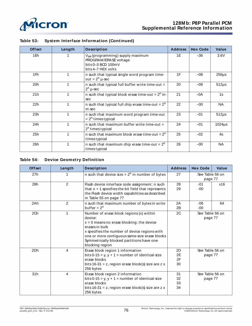
128Mb: P8P Parallel PCMSupplemental Reference Information
1Eh 1 VPP (programming) supply maximum PROGRAM/ERASE voltagebits 0–3 BCD 100mVbits 4–7 HEX volts
1E –36 3.6V
1Fh 1 n such that typical single word program time-out = 2n µ-sec
1F –08 256µs
20h 1 n such that typical full buffer write time-out = 2n µ-sec
20 –09 512µs
21h 1 n such that typical block erase time-out = 2n m-sec
21 –0A 1s
22h 1 n such that typical full chip erase time-out = 2n
m-sec22 –00 NA
23h 1 n such that maximum word program time-out = 2n times typical
23 –01 512µs
24h 1 n such that maximum buffer write time-out = 2n times typical
24 –01 1024µs
25h 1 n such that maximum block erase time-out = 2n
times typical25 –02 4s
26h 1 n such that maximum chip erase time-out = 2n
times typical26 –00 NA
Table 54: Device Geometry Definition
Offset Length Description Address Hex Code Value
27h 1 n such that device size = 2n in number of bytes 27 See Table 56 on page 77
28h 2 Flash device interface code assignment: n such that n + 1 specifies the bit field that represents the Flash device width capabilities as described in Table 55 on page 77
2829
-01-00
x16
2Ah 2 n such that maximum number of bytes in write buffer = 2n
2A2B
-06-00
64
2Ch 1 Number of erase block regions (x) within device:x = 0 means no erase blocking; the device erases in bulkx specifies the number of device regions with one or more contiguous same-size erase blocksSymmetrically blocked partitions have one blocking region
2C See Table 56 on page 77
2Dh 4 Erase block region 1 informationbits 0-15 = y, y + 1 = number of identical-size erase blocksbits 16-31 = z, region erase block(s) size are z x 256 bytes
2D2E2F30
See Table 56 on page 77
31h 4 Erase block region 2 informationbits 0-15 = y, y + 1 = number of identical-size erase blocksbits 16-31 = z, region erase block(s) size are z x 256 bytes
31323334
See Table 56 on page 77
Table 53: System Interface Information (Continued)
Offset Length Description Address Hex Code Value
PDF: 09005aef8447d46d/Source: 09005aef845b5c96 Micron Technology, Inc., reserves the right to change products or specifications without notice.parallel_pcm_2.fm - Rev. K 7/12 EN 76 ©2005 Micron Technology, Inc. All rights reserved.

128Mb: P8P Parallel PCMSupplemental Reference Information
35h 4 Reserved for future block erase block region information
35363738
See Table 56 on page 77
Table 55: Bit Field Definitions
Bit
7 6 5 4 3 2 1 0- - - - x64 x32 x16 x8
Bit
15 14 13 12 11 10 9 8- - - - - - - -
Table 56: Hex Code and Values for Device Geometry
Address
128Mb
-B -T
27 -18 -182829
0100
0100
2A2B
0600
0600
2C -02 -022D2E2F30
-03-00-80-00
-7E-00-00-02
31323334
-7E-00-00-02
-03-00-80-00
35363738
-00-00-00-00
-00-00-00-00
Table 54: Device Geometry Definition (Continued)
Offset Length Description Address Hex Code Value
PDF: 09005aef8447d46d/Source: 09005aef845b5c96 Micron Technology, Inc., reserves the right to change products or specifications without notice.parallel_pcm_2.fm - Rev. K 7/12 EN 77 ©2005 Micron Technology, Inc. All rights reserved.

128Mb: P8P Parallel PCMExtended Query Tables
Extended Query Tables
Table 57: Primary Vendor-Specific Extended Query
OffsetP = 10Ah Length Description (Optional Flash Features and Commands Address
Hex Code Value
(P + 0)h(P + 1)h(P + 2)h
3 Primary extended query table; unique ASCII string PRI 10A10B10C
-50-52-49
PRT
(P + 3)h 1 Major version number, ASCII 10D -31 1(P + 4)h 1 Minor version number, ASCII 10E -34 4(P + 5)h(P + 6)h(P + 7)h(P + 8)h
4 Optional feature and command support (1 = yes, 0 = no)bits 10-31 are reserved; undefined bit are 0. If bit 31 is 1, then another bit31 field of optional features follows at the end of the bit-30 fieldbit 0: Chip erase supportedbit 1: Suspend erase supportedbit 2: Suspend program supportedbit 3: Legacy lock/unlock supportedbit 4: Queued erase supportedbit 5: Instant individual block locking supportedbit 6: Protection bits supportedbit 7: Page mode read supportedbit 8: Synchronous read supportedbit 9: Simultaneous operations supportedbit 10: Extended Flash array blocks supportedbit 30: DFI link(s) to followbit 31: Another optional features field to follow
10F110111112
-E6-00-00-00
bit 0 = 0bit 1 = 1bit 2 = 1bit 3 = 0bit 4 = 0bit 5 = 1bit 6 = 1bit 7 = 1bit 8 = 0bit 9 = 0
bit 10 = 0bit 30 = 0bit 31 = 0
NoYesYesnoNoYesYesYesNoNoNoNoNo
(P + 9)h 1 Supported functions after suspend: read array, status, queryOther supported features include:bits 1-7: Reserved; undefined bits are 0bit 0: Program supported after erase suspend
113 -01bit 0 = 1 Yes
(P + A)h(P + B)h
2 Block status register maskbits 2-15: Reserved; undefined bits are 0bit 0: Block lock bit status register activebit 1: Block lock-down bit status activebit 4: EFA block lock bit status register activebit 5: EFA block lock-down bit status active
114115
-03-00
bit 0 = 1bit 1 = 1bit 4 = 0bit 5 = 0
YesYesNoNo
(P + C)h 1 VCC logic supply highest performance program/erase voltagebits 0-3: BCD value in 100mVbit 4-7: BCD value in volts
116 -33 3.3V
(P + D)h 1 VPP optimum program/erase supply voltagebits 0-3: BCD value in 100mVbit 4-7: Hex value in volts
117 -33 3.3V
Table 58: Protection Register Information
OffsetP = 10Ah Length Description (Optional Flash Features and Commands Address
Hex Code Value
(P + E)h 1 Number of protection register fields in JEDEC ID space000h indicates that 256 protection fields are available
118 -02 2
PDF: 09005aef8447d46d/Source: 09005aef845b5c96 Micron Technology, Inc., reserves the right to change products or specifications without notice.parallel_pcm_2.fm - Rev. K 7/12 EN 78 ©2005 Micron Technology, Inc. All rights reserved.

128Mb: P8P Parallel PCMExtended Query Tables
(P + F)h(P + 10)h(P + 11)h(P + 12)h
4 Protection field 1: Protection DescriptionThis field describes user-available one-time programmable (OTP) protection register bytes. Some are preprogrammed with device-unique serial numbers. Others are user-programmable. Bits 0-15 point to the protection register lock byte, the section’s first byte. The following bytes are factory preprogrammed and user-programmable.bits 0–7: Lock/bytes JEDEC-plane physical low addressbits 8–15: Lock/bytes JEDEC-plane physical high addressbits 16–23: n such that 2n = factory preprogrammed bytesbits 24–31 = n such that 2n = user-programmable bytes
11911A11B11C
-80-00-03-03
80h00h
8 byte8 byte
(P + 13)h(P + 14)h(P + 15)h(P + 16)h(P + 17)h(P + 18)h(P + 19)h(P + 1A)h(P + 1B)h(P + 1C)h
10 Protection field 2: Protection DescriptionBits 0-31 point to the protection register physical lock-word address in the JEDEC-plane. The following bytes are factory- or user-programmable
11D11E11F120
-89-00-00-00
89h00h00h00h
bits 32-39: = n ¬ n = factory programmed groups (low byte)bits 44739: = n n = factory programmed groups (high byte)bits 48-55: = n \ 2n = factory programmable bytes/group
121122123
-00-00-00
000
bits 56-63: = n ¬ n = user-programmed groups (low byte)bits 64-71: = n ¬ n = user-programmed groups (high byte)bits 72-79: = n ¬ 2n = user-programmable bytes/group
124125126
-10-00-04
160
16
Table 59: Read Information
OffsetP = 10Ah Length Description (Optional Flash Features and Commands Address
Hex Code Value
(P + 1D)h 1 Page mode read capabilitybits 0-7 = n such that 2n hex value represents the number of read-page bytes. See offset 28h for device word width to determine page mode data output width. 00h indicates no read page buffer.
127 -04 16 byte
(P + 1E)h 1 Number of synchronous mode read configuration fields that follow. 00h indicates no burst capability.
128 -00 0
Table 60: Partition and Erase Block Region Information
OffsetP = 10Ah
Description (Optional Flash Features and Commands
Address
Bottom Top Length Bottom Top
(P + 1F)h (P + 1F)h Number of device hardware-partition regions within the device.x = 0: a single hardware partition device (no fields follow)x specifies the number of device partition regions containing one or more contiguous erase block regions.
1 129 129
Partition Region 1 Information
(P + 20)h (P + 20)h Data size of this partition region information field (number of addressable locations, including this field)
2 12A12B
12A12B(P + 21)h (P + 21)h
(P + 22)h (P + 22)h Number of identical partitions within the partition region 2 12C12D
12C12D(P + 23)h (P + 23)h
Table 58: Protection Register Information (Continued)
OffsetP = 10Ah Length Description (Optional Flash Features and Commands Address
Hex Code Value
PDF: 09005aef8447d46d/Source: 09005aef845b5c96 Micron Technology, Inc., reserves the right to change products or specifications without notice.parallel_pcm_2.fm - Rev. K 7/12 EN 79 ©2005 Micron Technology, Inc. All rights reserved.
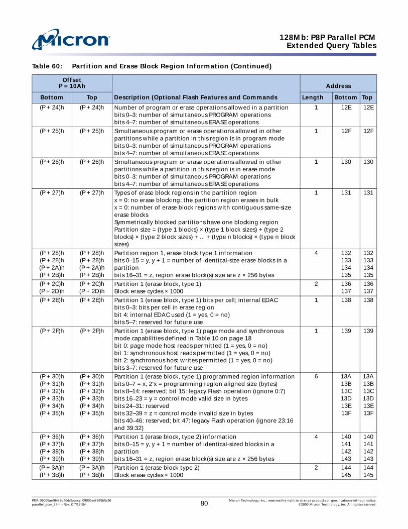
128Mb: P8P Parallel PCMExtended Query Tables
(P + 24)h (P + 24)h Number of program or erase operations allowed in a partitionbits 0–3: number of simultaneous PROGRAM operationsbits 4–7: number of simultaneous ERASE operations
1 12E 12E
(P + 25)h (P + 25)h Simultaneous program or erase operations allowed in other partitions while a partition in this region is in program modebits 0–3: number of simultaneous PROGRAM operationsbits 4–7: number of simultaneous ERASE operations
1 12F 12F
(P + 26)h (P + 26)h Simultaneous program or erase operations allowed in other partitions while a partition in this region is in erase modebits 0–3: number of simultaneous PROGRAM operationsbits 4–7: number of simultaneous ERASE operations
1 130 130
(P + 27)h (P + 27)h Types of erase block regions in the partition regionx = 0: no erase blocking; the partition region erases in bulkx = 0: number of erase block regions with contiguous same-size erase blocksSymmetrically blocked partitions have one blocking regionPartition size = (type 1 blocks) × (type 1 block sizes) + (type 2 blocks) × (type 2 block sizes) + ... + (type n blocks) × (type n block sizes)
1 131 131
(P + 28)h(P + 28)h(P + 2A)h(P + 2B)h
(P + 28)h(P + 28)h(P + 2A)h(P + 2B)h
Partition region 1, erase block type 1 informationbits 0–15 = y, y + 1 = number of identical-size erase blocks in a partitionbits 16–31 = z, region erase block(s) size are z × 256 bytes
4 132133134135
132133134135
(P + 2C)h(P + 2D)h
(P + 2C)h(P + 2D)h
Partition 1 (erase block, type 1)Block erase cycles × 1000
2 136137
136137
(P + 2E)h (P + 2E)h Partition 1 (erase block, type 1) bits per cell; internal EDACbits 0–3: bits per cell in erase regionbit 4: internal EDAC used (1 = yes, 0 = no)bits 5–7: reserved for future use
1 138 138
(P + 2F)h (P + 2F)h Partition 1 (erase block, type 1) page mode and synchronous mode capabilities defined in Table 10 on page 18bit 0: page mode host reads permitted (1 = yes, 0 = no)bit 1: synchronous host reads permitted (1 = yes, 0 = no)bit 2: synchronous host writes permitted (1 = yes, 0 = no)bits 3–7: reserved for future use
1 139 139
(P + 30)h(P + 31)h(P + 32)h(P + 33)h(P + 34)h(P + 35)h
(P + 30)h(P + 31)h(P + 32)h(P + 33)h(P + 34)h(P + 35)h
Partition 1 (erase block, type 1) programmed region informationbits 0–7 = x, 2^x = programming region aligned size (bytes)bits 8–14: reserved; bit 15: legacy Flash operation (ignore 0:7)bits 16–23 = y = control mode valid size in bytesbits 24–31: reservedbits 32–39 = z = control mode invalid size in bytesbits 40–46: reserved; bit 47: legacy Flash operation (ignore 23:16 and 39:32)
6 13A13B13C13D13E13F
13A13B13C13D13E13F
(P + 36)h(P + 37)h(P + 38)h(P + 39)h
(P + 36)h(P + 37)h(P + 38)h(P + 39)h
Partition 1 (erase block, type 2) informationbits 0–15 = y, y + 1 = number of identical-sized blocks in a partitionbits 16–31 = z, region erase block(s) size are z × 256 bytes
4 140141142143
140141142143
(P + 3A)h(P + 3B)h
(P + 3A)h(P + 3B)h
Partition 1 (erase block type 2)Block erase cycles × 1000
2 144145
144145
Table 60: Partition and Erase Block Region Information (Continued)
OffsetP = 10Ah
Description (Optional Flash Features and Commands
Address
Bottom Top Length Bottom Top
PDF: 09005aef8447d46d/Source: 09005aef845b5c96 Micron Technology, Inc., reserves the right to change products or specifications without notice.parallel_pcm_2.fm - Rev. K 7/12 EN 80 ©2005 Micron Technology, Inc. All rights reserved.

128Mb: P8P Parallel PCMExtended Query Tables
(P + 3C)h (P + 3C)h Partition 1 (erase block type 2) bits per cell; internal EDACbits 0–3: bits per cell in erase regionbit 4: internal EDAC used (1 = yes, 0 = no)bits 5–7: reserved for future use
1 146 146
(P + 3D)h (P + 3D)h Partition 1 (erase block, type 2) page mode and synchronous mode capabilities defined in Table 10 on page 18bit 0: page mode host reads permitted (1 = yes, 0 = no)bit 1: synchronous host reads permitted (1 = yes, 0 = no)bit 2: synchronous host writes permitted (1 = yes, 0 = no)bits 3–7: reserved for future use
1 147 147
(P + 3E)h(P + 3F)h(P + 40)h(P + 41)h(P + 42)h(P + 43)h
(P + 3E)h(P + 3F)h(P + 40)h(P + 41)h(P + 42)h(P + 43)h
Partition 1 (erase block, type 2) programming region informationbits 0–7 = x, 2^x = programming region aligned size (bytes)bits 8–14: reserved; bit 15: legacy Flash operation (ignore 0:7)bits 16–23 = y = control mode valid size in bytesbits 24–31: reservedbits 32–39 = z = control mode invalid size in bytesbits 40–46: reserved; bit 47: legacy Flash operation (ignore 23:16 and 39:32)
Table 61: Hex Code and Values for Partition and Erase Block Regions
Address
128Mb
-B -T
129 –01 –0112A12B
–24–00
–24–00
12C12D
–01–00
–01–00
12E –11 –1112F –00 –00130 –00 –00131 –02 –02132133134135
–03–00–80–00
–7E–00–00–02
136137
–64–00
–64–00
138 –01 –01139 –01 –0113A13B13C13D13E13F
–00–80–00–00–00–80
–00–80–00–00–00–80
Table 60: Partition and Erase Block Region Information (Continued)
OffsetP = 10Ah
Description (Optional Flash Features and Commands
Address
Bottom Top Length Bottom Top
PDF: 09005aef8447d46d/Source: 09005aef845b5c96 Micron Technology, Inc., reserves the right to change products or specifications without notice.parallel_pcm_2.fm - Rev. K 7/12 EN 81 ©2005 Micron Technology, Inc. All rights reserved.

128Mb: P8P Parallel PCMExtended Query Tables
140141142143
–7E–00–00–02
–03–00–80–00
144145
–64–00
–64–00
146 –01 –01147 –01 –0114814914A14B14C14D
–00–80–00–00–00–80
–00–80–00–00–00–80
Table 61: Hex Code and Values for Partition and Erase Block Regions (Continued)
Address
128Mb
-B -T
8000 S. Federal Way, P.O. Box 6, Boise, ID 83707-0006, Tel: 208-368-3900www.micron.com/productsupport Customer Comment Line: 800-932-4992
Micron and the Micron logo are trademarks of Micron Technology, Inc. All other trademarks are the property of their respective owners.This data sheet contains minimum and maximum limits specified over the power supply and temperature range set forth herein. Although
considered final, these specifications are subject to change, as further product development and data characterization sometimes occur.
PDF: 09005aef8447d46d/Source: 09005aef845b5c96 Micron Technology, Inc., reserves the right to change products or specifications without notice.parallel_pcm_2.fm - Rev. K 7/12 EN 82 ©2005 Micron Technology, Inc. All rights reserved.