(647 kb) - pier
TRANSCRIPT
Progress In Electromagnetics Research, Vol. 126, 49–64, 2012
PERFORMANCE-OPTIMIZED QUADRATE BOWTIE RFIDANTENNAS FOR COST-EFFECTIVE AND ECO-FRIENDLYINDUSTRIAL APPLICATIONS
Y. Amin1, *, Q. Chen, H. Tenhunen, and L. R. Zheng
iPack VINN Excellence Center, Royal Institute of Technology (KTH),Stockholm SE-16440, Sweden
Abstract—Fully integrated printed RFID antennas show potentialsolution for item level labeling applications. In order to accommodatethe antenna during the package printing process, it is vastly preferredthat antenna structures are printed on paper substrates. However,the electromagnetic properties and thickness of paper substrates aresusceptible to change due to various environmental effects. Thus,adequately consistent in performance and material insensitive printedQuadrate Bowtie RFID antennas are proposed. This paper presentsan in-depth efficient optimization for high performance tag antennadesigns for operability in frequencies 866–868 MHz & 902–928 MHz. Itis demonstrated that the proposed antennas can tolerate a considerablevariation in the permittivity on thin paper substrates, and presentbenchmarking results when n across metal and water containingobjects.
1. INTRODUCTION
As an ingredient of rapidly emerging technologies in automaticidentification and data capture (AIDC) industries, radio frequencyidentification (RFID) has been increasingly used in many applicationssuch as supply chain management, inventory control, securitymanagement, and logistics [1]. To meet the requirements for theseapplications, RFID tags need to be attached on various objects [2, 3]with different shapes and material properties. Therefore, an RFID tagantenna attached on a target object plays a crucial role in determiningthe overall performance of an RFID system. Presently much effortis dedicated to the development of RFID antennas by implementing
Received 8 February 2012, Accepted 1 March 2012, Scheduled 8 March 2012* Corresponding author: Yasar Amin ([email protected]).

50 Amin et al.
Table 1. Substrate parameters evaluated for proposed antennas.
SubstrateThickness
(µm)
Permittivity
(εr)Loss Tangent
Kodak Photopaper 280 3.2 (average) 0.077 (1 GHz@25C)
HP Photopaper 280 3.2 (average) 0.04 (1GHz@25C)
Paper (p e:smart) 250 3.2 (average) 0.077 (1 GHz@25C)
Metal coated PET 50 3.3 0.003 (0.9GHz@25C)
various technologies [4–6]; however, the development area appearsdeserted while encountering the issues interconnected to the field ofeconomic and eco-friendly tags comprising of paper substrate.
It often overlooked while mentioning the paper printed RFIDtags that use of paper defines the entirely new era of electricalperformance, which encounters from, new set of issues [7, 8]. Thepolymer-covered paper substrates have been used to demonstrateelectrochemical displays. While these paper coatings compromise thelow cost and recyclability, this might still be acceptable for relativelyhigh-value electronic applications that require relatively expensivematerials, several processing steps, and encapsulation [9]. Papersubstrates offer many advantages for printing RFID antennas, not onlyis paper widely available and affordable, it is lightweight, biodegradableand can be rolled or folded into 3D configurations [10, 11].
In this paper, novel quadrate bowtie passive RFID tag antennason paper/PET substrates are presented with the introduction ofimpedance matching approach to improve the reliability againstenvironmental diversities as well as increase the maximum readingdistance. The quadrate bowtie antenna [12] profile modification andT-matching network are used to match the antenna input impedanceto tag’s chip impedance, and the effects of metal and water onthe proposed antennas are also categorically investigated. TheEuropean and North American UHF RFID bands are preferred andall simulations are performed using ANSYS HFSSTM. These antennasare printed on different substrates (Table 1) using state-of-the-artprinting technologies (Dry Phase Patterning & Inkjet Printing). Themeasurements are carried out in an anechoic chamber along with thereader setup dedicated to antenna characterization for metal, andwater containing objects and proposed antennas are also comparedwith that of a commercial RFID tag. The ruggedness, eco-friendliness,flexibility and exceptionally long read range of these proposed antennasmake them an ideal choice for far-field cases, carton (containing water& metal objects) and (wood or metal) pallet industrial applications.
Progress In Electromagnetics Research, Vol. 126, 2012 51
2. ANTENNA DIMENSIONS AND PARAMETRICOPTIMIZATION
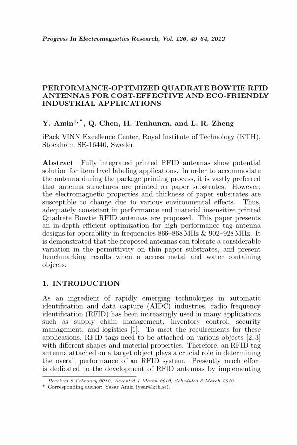
The proposed quadrate bowtie antennas are optimized on a methodicalbasis for minimizing the effects of environmental adversities on RFIDtags. The main purpose of enhancement is to maximize the feedingpower to the load and reduce the antenna area, while realizing thehighly efficient structures on paper substrate for eco-friendly tags.Figure 1 shows the Thevenin equivalent circuit of the IC tag, fromwhich the consumption power at the load is evaluated assuming theincident plane waves. In Figure 1, vo is received open voltage, Za =Ra + jXa the input impedance of the tag antenna, Zc = Rc + jXc
the impedance of the load, I the current flowing at the load. I andthe consumption power of the load Pc are obtained from (1) & (2):
I =vo
Za + Zc(1)
Pc = ReZcII∗ (2)
It is worth mentioning here that throughout the text onwardswhenever input impedance of antenna is referred it will be meant thatthe real part Ra of the antenna input impedance Za consists of theradiation resistance and the antenna losses or loss resistance. Hence,one of the optimization criteria is defined as (3),
kPc +(
1− S
Smax
)→ max (3)
where S is the antenna size and Smax the maximum size, and k inthe first term is the weighting constant to offset the first and secondterms. If the effect of the second term in the objective function istrivial, the impedance matching between Za and Zc will stand forthe optimal antenna, that is, Za of the optimized antenna will be thecomplex conjugate of Zc. Note that the input voltage vo depends on the
Figure 1. Far-field RFID mechanism & equivalent circuit of an ICtag.

52 Amin et al.
(a)
(b)
(c)
(e)
(d)
(f)
Figure 2. The geometry of RFID antenna for: (a) EU band, (b)NA band; DPP of antenna on PET for: (c) EU band, (d) NA band;inkjet printed antenna on: (e) HP photopaper for EU band, (f) Kodakphotopaper for NA band.
antenna structure in this problem [11]. Thus, it requires a conjugatematching technique such as series or parallel stubs. The matchingnetwork of the tag has to ensure the maximum power delivered to thechip. To achieve these design goals, a T-matched quadrate bowtieantenna (half wavelength dipole antenna) with rounded corners, isdesigned and fabricated. This design is used for the matching of thepassive antenna terminals to the NXP ucode g2xm (TSSOP8, e.g., thetarget IC impedance at 915MHz is 22-j191Ω). The prototype antennastructures for UHF RFID European (EU) band and North American(NA) is shown along with dimensions in Figures 2(a) & (b) respectively.The T-match arms are liable for impedance matching of the antennaterminals to that of the RFID chip through the fine tuning of the seriesand shunt stubs.
2.1. Antenna Effective Aperture
A commonly disregarded issue about an (RFID) antenna is howdirectivity and gain are correlated to its physical dimensions. Sincethe field/current, on the antenna aperture is not uniform, the conceptof antenna effective aperture is established to serve this purpose. Theeffective aperture Ae is less than the physical aperture Ap [13]. Thedirectivity D can also be articulated in expressions of the aperture size

Progress In Electromagnetics Research, Vol. 126, 2012 53
and aperture efficiency ηap:
D =4π
λ2Ae =
4π
λ2ηapAp (4)
where λ is the wavelength of the radio waves. By knowing the powerdensity S at the receiving antenna, we can approximate the receivedpower Pr:
Pr = SAe (5)
Thus during optimization course of action, much effort is devoted toimproving the effective aperture to increase the gain while maintainingthe low profile of the proposed antennas showed in Figure 2.
2.2. Skin Depth Effect and Antenna Performance
The skin depth and ohmic losses of the printed conductive layer set theboundary conditions for the manufacturing methods, and parameterssuch as the amount of silver ink and the thickness of the printed layers.Skin depth is one of the significant factors that lead to achieve a certainthickness of the conductive layer/s. Due to the skin effect at highfrequencies, e.g., at UHF, the current density is crowded in the regionnear the surface of a good conductor. More precisely the skin depth isthe depth below the surface of the conductor at which the amplitudeof the incident electric field decays to 0.37% of the amplitude at thesurface of the conductor. Mathematically, the skin depth δ in case ofa good conductor is, therefore [13], expressed as:
δ ≈√
1πfµσ
(6)
where f is the frequency, µ is the permeability and σ is the conductivityof the conductor material. Thus from above we can deduce three keyconclusions that surround the manufacturing process of the proposedantennas:
(i) The higher the frequency, (in this particular case, 860–960MHz),the smaller the skin depth.
(ii) The higher the permeability (in case, it is not that high, whichneeds attention while printing process), the smaller the skin depth.However for a good conductor, the permittivity has little effect onthe skin depth.
(iii) The higher the conductivity (in case, the conductivity of theprinted structure is almost 5 times lower than that of bulksilver due to several parametric constrains in manufacturing), thesmaller the skin depth.

54 Amin et al.
3. DPP AND INKJET PRINTING: CONDUCTIVEFEATURES
The standard antenna structures for comparison and validation of theconcept are fabricated using Dry Phase Patterning (DPP). It is asingle step method for patterning metal or polymer layers on mostflexible substrates. The laminate of Aluminum (10µm layer)/PET ispatterned for proposed antennas showed in Figures 2(c) & (d) in onesingle step, unlike in a wet etching process that involves 6–8 steps toachieve the same pattern. Acreo AB has reported patterning resolutionof as small as 200µm and speed up to 150 m/min, which made it abetter choice for cost effective RFID tags.
In addition to cutting down on waste and providing an all-in-one substitute to cleanroom deposition technologies, inkjet printingcharacteristics with regards to accuracy and form make it anexceptionally pleasant contestant for RF circuits. The practicabilityof inkjet printing for applications at UHF frequencies has been wellcovered under [9]. The Cabot conductive ink (CCI-300) by CabotCorp., is used to print these proposed antennas, which contains 19–21% weight of nano-silver particles of less than 20 nm diameter. Thelarge ratio of the area to volume of these nano-silver particles exhibitthe significantly lower melting point even less than 100C. The inkjetprinting is carried out utilizing DMP2800 inkjet printer, as showedin Figure 3(a) which is a table-top printer available from DimatixInc. To realize substantial RF properties, the printing resolution of1000 dpi (Dimatix 10 pL cartridge) −2540 dpi (Dimatix 1 pL cartridge)is achieved by adjusting the print head and it is figured out thatusing this technique a printing resolution of 1000 dpi is suitable forfrequencies in the UHF range. Figure 3(b) shows the surface profile ofan RFID antenna printed using cartridges jetting out ink droplets. Theink is then jetted at a temperature of 40C, while the paper substratementioned in Table 1 is maintained at 60C. In all print setups, thesubstrate is kept at a distance of 0.5 mm from the print head. Toensure reliable RF conductivity, three layers of ink are printed whichresults in a thickness of around 3µm while using a heat gun to annealin between each re-printing cycle.
After printing, the deposited ink also needs to be annealed toensure adjacent silver nanoparticles in the jetted ink to coagulate withneighbors, allowing for a smoother path for electron flow particularlyat high frequencies. Each printed structure is cured in a thermaloven for two hours at 120 resulting into a consistent, measured DCconductivity in the range 9 × 10⁶ [S/m] −1.1 × 10⁷ [S/m]. Theconductivity of the printed structure can also be further increased

Progress In Electromagnetics Research, Vol. 126, 2012 55
(a) (b)
Figure 3. (a) Inkjet printing setup, (b) drop watcher view (top)showing ink printed out of nozzles & images by Fiducial camera ofDMP-2800 for inspection of printed ink layer.
by using a higher print resolution setting on the printer. Antennatraces with exceptionally meritorious conductivity and the pitches areaccurately fabricated using this inkjet printing process, and is shownby the close-up of a printed trace in Figure 3(b).
4. RESULT ANALYSIS AND DISCUSSION
Passive RFID tags for European and North American UHF RFIDbands are manufactured with different substrates mentioned in Table 1,are measured across the frequency band of interest using half mirrormethod to investigate the reliability aspects of the proposed antennasfor commercial grade practices. Ten identical prototypes of proposedstructures are manufactured on an each paper substrate in order todetermine the worst case analysis ingredients. Thus, each curve inFigure 4 represents the highest deviated values at a certain pointamong identical samples.
Impedance measurements are taken using vector network analyzer(MS2026B, Anritsu). The standard calibration procedure short-open-load (SOL) is adopted for accuracy of results. In order toverify the performance of the inkjet printed antennas of Figures 2(e)& (f), measurements are also executed using standard antennaprototypes fabricated on Aluminum coated PET substrate as showedin Figures 2(c) & (d). These standard prototypes have the samedimensions as that of proposed antennas and are fabricated usingDPP (Dry Phase Patterning) process at Acreo AB. The impedancevariation of antenna in Figure 2(a) is shown in Figures 4(a) & (b).Whereas, input impedance plots of antenna in Figure 2(b) are shown

56 Amin et al.
(a) (b)
(c) (d)
Figure 4. EU band’s antenna input: (a) (radiation & loss) resistancevariation, (b) reactance variation; NA band’s antenna input: (c)(radiation & loss) resistance variation, (d) reactance variation.
in Figures 4(c) & (d). The resistive parts of impedance as showed inFigures 4(a) & (c) for EU and NA band antennas respectively, printedon different photopapers demonstrate consistency to the DPP antennas& simulated results throughout frequency band of interest which isa primary concern for antennas stable behavior. However, slightlygreater drift is observed in the resistive part of the antennas printedon paper (p e:smart) from Felix Schoeller as compared to the othersbut the difference remains within the acceptable range. Similarly,fairly coherent trend of reactance curves is depicted in Figures 4(b)& (d) for both proposed structures. The formation of round cornersis used to obtain wider impedance band. Round corners at the sharpvertexes decreases the reflection of incident current near the edges andchanges the current distribution on radiation surfaces. Thus, flatterimpedance within the frequency band of interest with much stable real

Progress In Electromagnetics Research, Vol. 126, 2012 57
and imaginary parts is demonstrated in Figure 4.Using the Friis equation, the read range which is one of the
most dominant tag performance characteristics can be estimated byEquation (7) defining forward-link-limited range and Equation (8)defining reverse-link-limited range. Read range is also susceptibleto the tag orientation, the object which the tag is placed on,path loss, spatial and temporal fading statistics of the propagationenvironment [14].
Rforward =(
λ
4π
) √PTXGreaderGtag
Pmin,tag(7)
and defining the minimum signal power for demodulation at the readeras Pmin,rdr we obtain the reverse-link-limited range:
Rreverse =(
λ
4π
)4
√PTX,readerTbG
2readerG
2tag
Pmin,rdr(8)
where the output power of the reader is PTX , the gain of the readerantenna is Greader , and the gain of the tag antenna is Gtag. λ isthe wavelength in free space at the operating frequency, Pmin is theminimum power required to turn on the tag chip and Tb is backscattertransmission loss.
The read range from Equations (7) & (8) gives the maximumdistance at which RFID reader can interpret the tag in free space.Thus, this statement of read range is invalid at near-field distances. Inthe near-field region, the E and H-fields are not orthogonal so anythingwithin this region couples with the antenna and distort the pattern;thus, the antenna gain is not a valid parameter here. Therefore,the near-field performance testing is carried out inside the anechoicchamber with Impinj’s UHF RFID reader kit. The far-field distanceis calculated by (2D2/λ), and it is observed as an estimate becausethe transition from near-field to far-field is not instantaneous. The D(maximum dimension of the radiating structure) of the reader antennaused is 0.3m (1foot), thus in measurements which are taken at 915 MHz(λ = 0.33m) the far-field distance is estimated to be 0.56 m. Theproposed antennas exhibit superior readability within reactive near-field region. It is observed that, in the near-field region the antennapattern is taking shape but is not fully formed, and the antenna gainmeasurements vary with distance.
In most UHF RFID systems, the reading distance obtained byEquations (7) & (8) extends well into the far-field region. When thereis an implementation of tag which can operate in the far-field alsoinvolves near-field tag scanning. It can be expected that, in almost all

58 Amin et al.
cases, the tag gets more than sufficient power to operate when broughtcloser to RFID reader antenna. Hence, the read range of most UHFRFID tags is determined by the tag working in the far-field [15]. Theproposed antennas have surpassed read range from 6.5m (HP) – 7.0 mdepending upon which substrate is utilized. Furthermore, the detailedanalysis of read range variation is presented in Tables 2 & 3.
The return loss results of antennas in Figures 4(a) & (b) is shownin Figures 5(a) & (b) respectively. It is pragmatic that the return lossof the inkjet printed antennas is slightly higher than the return loss ofstandard PET substrate antennas. Overall, good agreement betweenthe standard PET-based, and the inkjet printed antennas is observed,regardless of the higher metal loss of the silver based conductive ink.The distortion is possibly due to the effect of metal ground fixture usedfor half mirror method [16].
The most challenging in measurement steps, the radiation patternof antennas is measured in an anechoic chamber setup that replicateabsolute free space which is presented in Figure 6. The antennaunder test (AUT) is mounted over the positioner assembly in the
Table 2. Analysis of effect by metal on the proposed tag at 915 MHz.
Measured → • Input Radiation Trans. Directivity Gain Reading
Computed → ∗ impedance efficiency coeff. (dBi)∗ (dBi) ∗ range, R
(Ω)• (%)∗ (dB)∗ (m)•Free space 24.42 + j194.92 83.64 −1.07 1.85 1.97 6.50
d = 1 mm 4.31 + j152.13 1.02 −13.57 7.96 −10.37 0.31
d = 5 mm 5.76 + j173.06 6.61 −9.97 8.26 −1.12 1.14
d = 10mm 7.75 + j186.55 18.02 −3.53 8.29 0.58 3.22
d = 15mm 10.17 + j193.10 30.67 −0.67 8.28 2.92 8.10
Table 3. Analysis of effect by water on the proposed tag at 915MHz.
Measured → • Input Radiation Trans. Directivity Gain Reading
Computed → ∗ impedance efficiency coeff. (dBi)∗ (dBi)∗ range, R
(Ω)• (%)∗ (dB)∗ (m)•Free space 24.42 + j194.92 83.64 −1.07 1.85 1.97 6.50
d = 1mm 129.27 + j330.00 8.77 −9.51 4.12 −7.51 0.61
d = 5mm 23.61 + j201.20 6.29 −1.32 2.67 −10.05 1.15
d = 10mm 13.77 + j189.04 20.26 −0.33 2.81 −3.02 3.23
d = 15mm 12.20 + j189.90 27.64 −0.15 3.73 −1.13 4.37
d = 20mm 10.21 + j190.82 38.31 −0.08 4.93 −0.12 5.26

Progress In Electromagnetics Research, Vol. 126, 2012 59
(a) (b)
Figure 5. Return loss of antennas for: (a) EU band, (b) NA band.
Figure 6. The anechoic chamber & instruments used.
(a) (b)
Figure 7. Measured & computed 2D far-field radiation plots ofantennas for: (a) EU band, (b) NA band.

60 Amin et al.
center of the chamber which is set to rotate the antenna in smallsteps of 5 degrees to obtain a 360 radiation pattern. A continuous-wave (CW) signal from the signal generator excites the AUT. Thereceiver antenna is connected to the spectrum analyzer (Agilent HP8562E) and a PC running the test automation software controls themeasurement setup. Soft soldering is avoided to fix the AUT to thetest fixture since it requires heating the filler metal above 250C toachieve proper soldering, but this temperature severely damages theprinted traces on paper substrates. Thus, antennas are attached to thetest terminal with CW2400 silver conductive epoxy, cured at 24C for4 hours to reach maximum conductivity and adhesion. The normalizedcomputed radiation pattern and the microwave chamber measurementsare plotted in Figure 7. The radiation patterns are nearly uniform(omnidirectional) at 915MHz. They show remarkably satisfactoryagreement between computations and measurements. The sameuniformity in antenna radiation pattern could be demonstrated forother frequencies within the antenna’s bandwidth. Similar parametricbehavior is depicted by proposed antennas for EU band, which areshown in Figures 2(a), (c) & (e).
5. ANALYSIS FOR INDUSTRIAL APPLICATIONS
5.1. Effects of Metal on Tag Antenna Performance
The metal effect is limited in the tag antenna which has its own groundplane [17, 18]. However, the antenna which does not have a groundplane, such as quadrate bowtie, the radiation characteristics and inputimpedance of the antenna, are distorted when the tag is placed on ornear a metal object. Whenever there is an encounter with metal objectsthese variations certainly impact the tag performance [5]; however,even if it is not possible to eliminate it completely [3]; it is madepossible in the proposed antennas to, strongly limit this phenomenon.
The comprehensive data on the metal effect on the proposed RFIDtag antenna placed close to a metal plate and reading distance at915MHz is summarized in Table 2. The antenna is positioned parallelto and below a metal plate measuring 30 cm× 30 cm. The directivity,radiation efficiency, gain, and input impedance, are examined for thedifferent distances from the metal plate. Considering the worst case,i.e., when the antenna is placed extremely close to the metal plate(d = 1 mm), the directivity of the antenna enhances significantly toaround 8 dBi. However, the radiation efficiency plunges drastically to1.02%, which results in remarkably low gain of −10.37 dBi at 915 MHz.Particularly, the real part of the input impedance varies severely, aswell. This variation in impedance outcome in deprived impedance
Progress In Electromagnetics Research, Vol. 126, 2012 61
matching with the RFID tag chip (circuit showed in Figure 1), resultingin a transmission loss of−13.57 dB at 915MHz. The gain reduction andpoor impedance matching results in the reading distance reducing to0.31m. However, the proposed antenna still exhibited superior readingdistance when placed so closer to the metal object in coherence withpreviously published results [3, 18].
The directivity of the antenna remains virtually unchanged, bymoving the antenna further away from the metal plate. In themeantime, the radiation efficiency shows an escalating drift, whichdomino result in increasing antenna gain. The real part of the inputimpedance shows modest change, whereas the imaginary part inclinedto values close to those in free space. An increasing trend is observedin the reading distance; when the tag is moved away from the metalplate. When the tag is moved to d = 5 mm, the reading distanceexhibits higher value than that of in free space because the metalplate acts as a reflector which ultimately boosts the tag antenna gain.In conclusion, although the metal object degrades the reading rangeof the tag significantly when it is directly attached or is placed realclose to it, but the proposed antennas are even capable of reasonablycommunicating under these critical testing conditions.
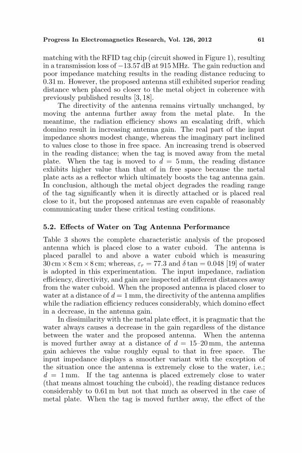
5.2. Effects of Water on Tag Antenna Performance
Table 3 shows the complete characteristic analysis of the proposedantenna which is placed close to a water cuboid. The antenna isplaced parallel to and above a water cuboid which is measuring30 cm×8 cm×8 cm; whereas, εr = 77.3 and δ tan = 0.048 [19] of wateris adopted in this experimentation. The input impedance, radiationefficiency, directivity, and gain are inspected at different distances awayfrom the water cuboid. When the proposed antenna is placed closer towater at a distance of d = 1 mm, the directivity of the antenna amplifieswhile the radiation efficiency reduces considerably, which domino effectin a decrease, in the antenna gain.
In dissimilarity with the metal plate effect, it is pragmatic that thewater always causes a decrease in the gain regardless of the distancebetween the water and the proposed antenna. When the antennais moved further away at a distance of d = 15–20 mm, the antennagain achieves the value roughly equal to that in free space. Theinput impedance displays a smoother variant with the exception ofthe situation once the antenna is extremely close to the water, i.e.;d = 1 mm. If the tag antenna is placed extremely close to water(that means almost touching the cuboid), the reading distance reducesconsiderably to 0.61 m but not that much as observed in the case ofmetal plate. When the tag is moved further away, the effect of the

62 Amin et al.
water is declined; resulting in read range enhancement. Therefore,exhibiting the graceful degradation in functionality for suitability inhigh performance industrial applications. The proposed antennasexhibit improved performance and are in accordance with commerciallyavailable RFID tags and previously published results [20].
Furthermore, the metallic plate and water do not degrade thebandwidth of the proposed antennas to such an extent that theybecome unreadable until the tag is placed closer than d = 1 mm.The bandwidth degradation behavior is constant, in case the tag isbrought nearer to the water containing objects, but in case of metallicplate, the bandwidth degradation is more serious particularly withind = 5 mm. The proposed antennas are designed with reasonablywideband in order to demonstrate readable bandwidth at the expenseof read range (bandwidth vs. read range trade-off) which limits theirusage to narrow bandwidth operations, i.e., either for EU band orNA band. The stabilization of bandwidth can further be achieved byreducing the effect of matching network, but that will induce instabilityagainst dielectric variation of paper substrate, so it is trade-off alwaysamong optimum values depending upon the applications.
6. CONCLUSION
The novel quadrate bowtie antennas for UHF RFID industrialapplications have been proposed and fabricated on paper and PETsubstrates, using inkjet printing and DPP technology respectively.In addition to categorical optimization of antenna profile, a T-matching network is introduced to develop a novel compact, RFIDtag, featuring outstanding overall performance. The antennas exhibitexceptional operational characteristics when stumble upon metal andwater containing objects. The use of the inkjet printing process in thedevelopment of these proficient RFID antennas on different types ofpaper has also been demonstrated, verifying that paper-based inkjetprinting topologies offer a remarkably low-cost, “green” solution tosystem-level packaging for UHF, wireless, and microwave applications.
ACKNOWLEDGMENT
The author would like to thank Peter Fuks in school of electricalengineering at KTH who generously provided measurement facilities.This work was financially supported by Vinnova (The SwedishGovernmental Agency for Innovation Systems) through the VinnExcellence centers program and by the EU project CLIP of grantnumber 243557 through EU FP7-SME-2008-2.

Progress In Electromagnetics Research, Vol. 126, 2012 63
REFERENCES
1. Zuo, Y., “Survivable RFID systems: Issues, challenges, andtechniques,” IEEE J. SMCC , Vol. 40, No. 4, 406–418, 2010.
2. Tiang, J.-J., M. T. Islam, N. Misran, and J. S. Mandeep, “Circularmicrostrip slot antenna for dual-frequency RFID application,”Progress In Electromagnetics Research, Vol. 120, 499–512, 2011.
3. Chen, S.-L., S.-K. Kuo, and C.-T. Lin, “A metallic RFID tagdesign for steel-bar and wire-rod management application in thesteel industry,” Progress In Electromagnetics Research, Vol. 91,195–212, 2009.
4. Panda, J. R. and R. S. Kshetrimayum, “A printed2.4GHz/5.8 GHz dual-band monopole antenna with a protrudingstub in the ground plane for WLAN and RFID applications,”Progress In Electromagnetics Research, Vol. 117, 425–434, 2011.
5. Hsu, H.-T., F.-Y. Kuo, and C.-H. Chang, “Application ofquasi log-periodic antenna for UHF passive RFID tag designfeaturing constant power transmission coefficient over broadbandoperation,” Journal of Electromagnetic Waves and Applications,Vol. 24, Nos. 5–6, 575–586, 2010.
6. Jamlos, M. F., T. A. Rahman, M. R. Kamarudin, P. Saad,M. A. Shamsudin, and A. M. M. Dahlan, “A novel adaptive Wi-Fi system with RFID technology,” Progress In ElectromagneticsResearch, Vol. 108, 417–432, 2010.
7. Alimenti, F., M. Virili, G. Orecchini, P. Mezzanotte, V. Palazzari,M. M. Tentzeris, and L. Roselli, “A new contactless assemblymethod for paper substrate antennas and UHF RFID chips,”IEEE Transactions on Microwave Theory and Techniques, Vol. 59,No. 3, 627–637, 2011.
8. Lazaro, A., D. Girbau, and R. Villarino, “Effects of interferencesin UHF RFID systems,” Progress In Electromagnetics Research,Vol. 98, 425–443, 2009.
9. Tobjerk, D. and R. Osterbacka, “Paper electronics,” Adv. Mater.,Vol. 23, No. 17, 1935–1961, 2011.
10. Bose, I. and S. Yan, “The green potential of RFID projects: Acase-based analysis,” IEEE IT Pro., Vol. 13, No. 1, 41–47, 2011.
11. Makimura, H., Y. Watanabe, K. Watanabe, and H. Igarashi,“Evolutional design of small antennas for passive UHF-bandRFID,” IEEE J. MAG , Vol. 47, No. 5, 1510–1513, 2011.
12. Qu, S.-W. and C.-L. Ruan, “Effect of round corners on bowtieantennas,” Progress In Electromagnetics Research, Vol. 57, 179–

64 Amin et al.
195, 2006.13. Huang, Y. and K. Boyle, Antennas from Theory to Practice, John
Wiley & Sons Ltd., New York, 2008.14. Nikitin, P. V. and K. V. Rao, “Antennas and propagation in UHF
RFID systems,” IEEE International Conference on RFID , 277–288, 2008.
15. Tikhov, Y., “Comments on ‘antenna design for UHF RFID tags:A review and a practical application,” IEEE J. AP , Vol. 54, No. 6,2006.
16. Kuo, S.-K., S.-L. Chen, and C.-T. Lin, “An accurate methodfor impedance measurement of RFID tag antenna,” Progress InElectromagnetics Research, Vol. 83, 93–106, 2008.
17. Sanchez-Montero, R., S. Salcedo-Sanz, J. A. Portilla-Figueras,and R. Langley, “Hybrid pifa-patch antenna optimized by evo-lutionary programming,” Progress In Electromagnetics Research,Vol. 108, 221–234, 2010.
18. Lin, D. B., I.-T. Tang, and C.-C. Wang, “UHF RFID H-shaped tagantenna using microstrip feed design on metallic objects,” Journalof Electromagnetic Waves and Applications, Vol. 25, No. 13, 1828–1839, 2011.
19. Xi, J., H. Zhu, and T. T. Ye, “Platform-tolerant PIFA-type UHFRFID tag antenna,” International IEEE Conference on RFID ,174–180, 2010.
20. Bjorninen, T., A. Z. Elsherbeni, and L. Ukkonen, “Low-profileconformal UHF RFID tag antenna for integration with waterbottles,” IEEE J. AWPL, Vol. 10, 1147–1150, 2011.