max2 23.mh to mh fractional/ integer-n … 23.mh to mh fractional/ integer-n synthesier/vco general...
TRANSCRIPT
Ordering Information appears at end of data sheet.
Typical Application Circuit appears at end of data sheet.
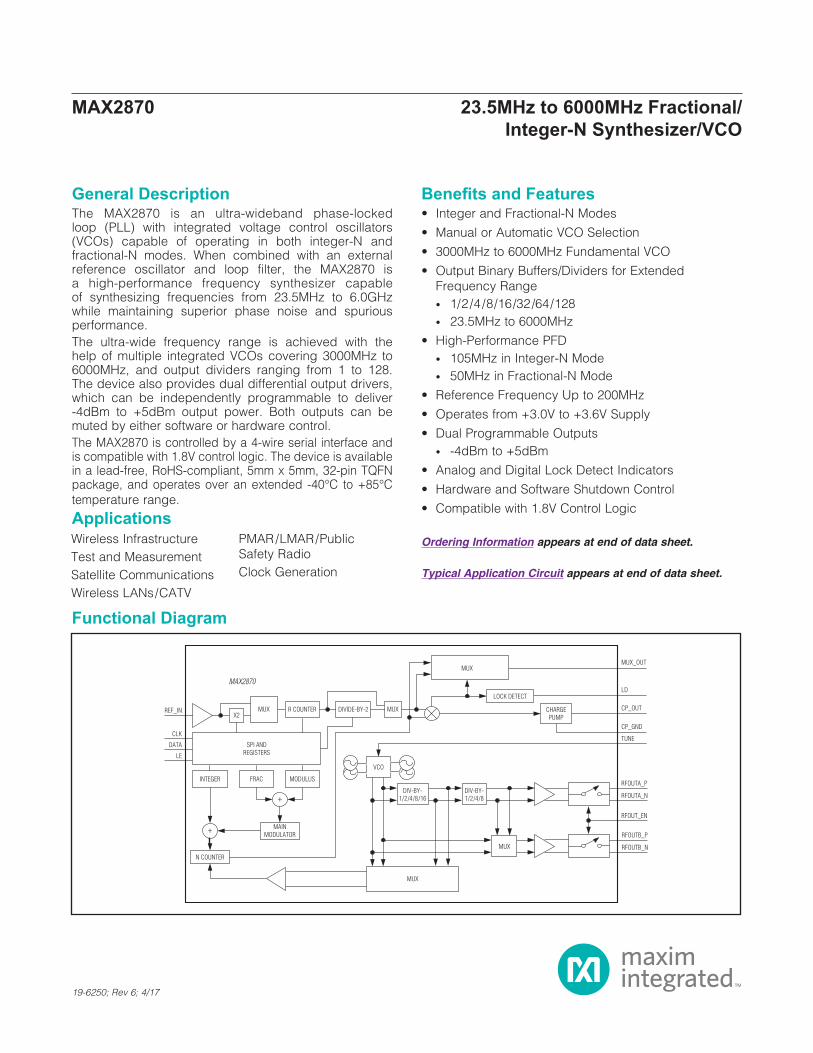
Functional Diagram
MAX2870 23.5MHz to 6000MHz Fractional/ Integer-N Synthesizer/VCO
General DescriptionThe MAX2870 is an ultra-wideband phase-locked loop (PLL) with integrated voltage control oscillators (VCOs) capable of operating in both integer-N and fractional-N modes. When combined with an external reference oscillator and loop filter, the MAX2870 is a high-performance frequency synthesizer capable of synthesizing frequencies from 23.5MHz to 6.0GHz while maintaining superior phase noise and spurious performance.The ultra-wide frequency range is achieved with the help of multiple integrated VCOs covering 3000MHz to 6000MHz, and output dividers ranging from 1 to 128. The device also provides dual differential output drivers, which can be independently programmable to deliver -4dBm to +5dBm output power. Both outputs can be muted by either software or hardware control.The MAX2870 is controlled by a 4-wire serial interface and is compatible with 1.8V control logic. The device is available in a lead-free, RoHS-compliant, 5mm x 5mm, 32-pin TQFN package, and operates over an extended -40NC to +85NC temperature range.
Applications
Benefits and FeaturesU Integer and Fractional-N Modes
U Manual or Automatic VCO Selection
U 3000MHz to 6000MHz Fundamental VCO
U Output Binary Buffers/Dividers for Extended Frequency Range
• 1/2/4/8/16/32/64/128 • 23.5MHz to 6000MHz
U High-Performance PFD • 105MHz in Integer-N Mode • 50MHz in Fractional-N Mode
U Reference Frequency Up to 200MHz
U Operates from +3.0V to +3.6V Supply
U Dual Programmable Outputs • -4dBm to +5dBm
U Analog and Digital Lock Detect Indicators
U Hardware and Software Shutdown Control
U Compatible with 1.8V Control Logic
Wireless InfrastructureTest and MeasurementSatellite CommunicationsWireless LANs/CATV
PMAR/LMAR/Public Safety RadioClock Generation
REF_IN
CLK
DATA
LE
X2MUXMUX DIVIDE-BY-2R COUNTER
INTEGER FRAC
MAINMODULATOR
MODULUS
VCO
SPI ANDREGISTERS
DIV-BY-1/2/4/8
MUX
DIV-BY-1/2/4/8/16
MUX
MUX
LOCK DETECT
CHARGEPUMP
MUX_OUT
LD
CP_OUT
CP_GND
TUNE
RFOUTA_P
RFOUTB_P
RFOUT_EN
RFOUTA_N
RFOUTB_N
N COUNTER
MAX2870
19-6250; Rev 6; 4/17

VCC_to GND_ .......................................................-0.3V to +3.9VAll Other Pins to GND_ .............................. -0.3V to VCC_ + 0.3VContinuous Power Dissipation (TA = +70NC) TQFN-EP Multilayer Board (derate 34.5mW/NC above +70NC) .........................2758.6mW
Junction Temperature .....................................................+150NCOperating Temperature Range .......................... -40NC to +85NCStorage Temperature Range ............................ -65NC to +150NCLead Temperature (soldering, 10s) .............................. +300NCSoldering temperature (reflow) .......................................+260NC
TQFN Junction-to-Ambient Thermal Resistance (BJA) ..........29NC/W Junction-to-Case Thermal Resistance (BJC) ..................1.7NC/W
Absolute Maximum Ratings
Note 1: Package thermal resistances were obtained using the method described in JEDEC specification JESD51-7, using a four-layer board. For detailed information on package thermal considerations, refer to www.maximintegrated.com/thermal-tutorial.
Stresses beyond those listed under “Absolute Maximum Ratings” may cause permanent damage to the device. These are stress ratings only, and functional opera-tion of the device at these or any other conditions beyond those indicated in the operational sections of the specifications is not implied. Exposure to absolute maximum rating conditions for extended periods may affect device reliability.
Package Thermal Characteristics (Note 1)
DC Electrical Characteristics(Measured using MAX2870 EV Kit. VCC_ = 3V to 3.6V, VGND_ = 0V, fREF_IN = 50MHz, fPFD = 25MHz, TA = -40NC to +85NC. Typical values measured at VCC_ = 3.3V; TA = +25NC; register settings (Reg 0:5) 00780000,20000141,01005E42,00000013,610F423C,01400005; unless otherwise noted.) (Note 2)
AC Electrical Characteristics(Measured using MAX2870 EV Kit. VCC_ = 3V to 3.6V, VGND_ = 0V, fREF_IN = 50MHz, fPFD = 25MHz, fRFOUT_ = 6000MHz, TA = -40NC to +85NC. Typical values measured at VCC_ = 3.3V, TA = +25NC, register settings (Reg 0:5) 00780000,20000141,01005E42,00000013,610F423C,01400005; unless otherwise noted.) (Note 2)
MAX2870 23.5MHz to 6000MHz Fractional/ Integer-N Synthesizer/VCO
www.maximintegrated.com Maxim Integrated 2
PARAMETER CONDITIONS MIN TYP MAX UNITS
Supply Voltage 3 3.3 3.6 V
RFOUT_ Current ConsumptionIRFOUT_, minimum output power, single channel 8.5
mAIRFOUT_, maximum output power, single channel 25 29
Supply Current
Both channels enabled, maximum output power
Total, including RFOUT, both channel (Note 3)
144 180
mAEach output divide-by-2 10 15
ICCVCO + ICCRF (Note 3) 75 95
Low-power sleep mode 1
PARAMETER CONDITIONS MIN TYP MAX UNITS
REFERENCE OSCILLATOR INPUT (REF_IN)
REF_IN Input Frequency Range 10 200 MHz
REF_IN Input Sensitivity 0.7 VCC_ VPP
REF_IN Input Capacitance 2 pF
REF_IN Input Current -60 +60 FA
PHASE DETECTOR
Phase Detector FrequencyInteger-N mode 105
MHzFractional-N mode 50
AC Electrical Characteristics (continued)(Measured using MAX2870 EV Kit. VCC_ = 3V to 3.6V, VGND_ = 0V, fREF_IN = 50MHz, fPFD = 25MHz, fRFOUT_ = 6000MHz, TA = -40NC to +85NC. Typical values measured at VCC_ = 3.3V, TA = +25NC, register settings (Reg 0:5) 00780000,20000141,01005E42,00000013,610F423C,01400005; unless otherwise noted.) (Note 2)
MAX2870 23.5MHz to 6000MHz Fractional/ Integer-N Synthesizer/VCO
www.maximintegrated.com Maxim Integrated 3
PARAMETER CONDITIONS MIN TYP MAX UNITS
CHARGE PUMP
Sink/Source CurrentCP[3:0] = 1111, RSET = 5.1kI 5.12
mACP[3:0] = 0000, RSET = 5.1kI 0.32
RSET Range 2.7 10 kI
RF OUTPUTS
Fundamental Frequency Range 3000 6000 MHz
Divided Frequency Range With output dividers (1/2/4/8/16/32/64/128) 23.4375 6000 MHz
VCO Sensitivity 100 MHz/V
Frequency Pushing Open loop 0.7 MHz/V
Frequency Pulling Open loop into 2:1 VSWR 70 KHz
2nd Harmonic Fundamental VCO output 40 dBc
3rd Harmonic Fundamental VCO output 34 dBc
2nd Harmonic VCO output divided-by-2 20 dBc
3rd Harmonic VCO output divided-by-2 21 dBc
Maximum Output Power fRFOUT_ = 3000MHz (Note 4) 5 dBm
Minimum Output Power fRFOUT_ = 3000MHz (Note 4) -4 dBm
Output Power Variation (Note 4)-40NC P TA P +85NC 1.5
dB3V P VCC_ P 3.6V 0.2
Muted Output Power (Note 4) -31 dBm
VCO AND FREQUENCY SYNTHESIZER NOISE
VCO Phase Noise (Note 5)
VCO at 3000MHz
10kHz offset -83.5
dBc/Hz
100kHz offset -111
1MHz offset -136
5MHz offset -149
VCO at 4500MHz
10kHz offset -75
100kHz offset -104
1MHz offset -130
5MHz offset -145.5
VCO at 6000MHz
10kHz offset -71.5
100kHz offset -100.5
1MHz offset -128.0
5MHz offset -143.5
In-Band Noise Floor Normalized (Note 6) -226.4 dBc/Hz
1/f Noise Normalized (Note 7) -116 dBc/Hz
In-Band Phase Noise (Note 8) -95 dBc/Hz
Integrated RMS Jitter (Note 9) 0.25 ps
Spurious Signals Due to PFD Frequency -87 dBc
VCO Tune Voltage 0.5 2.5 V
Digital I/O Characteristics(VCC_ = +3V to +3.6V, VGND_ = 0V, TA = -40NC to +85NC. Typical values at VCC_ = 3.3V, TA = +25NC.) (Note 2)
SPI Timing Characteristics(VCC_ = +3V to +3.6V, VGND_ = 0V, TA = -40NC to +85NC. Typical values at VCC_ = 3.3V, TA = +25NC.) (Note 2)
Note 2: Production tested at TA = +25NC. Cold and hot are guaranteed by design and characterization.Note 3: fREFIN = 100MHz, phase detector frequency = 25MHz, RF output = 6000MHz.
Register setting: 00780000, 20400061, 20011242, F8010003, 608001FC, 80440005Note 4: Measured single ended with 27nH to VCC_RF into 50I load. Power measured with single output enabled. Unused output
has 27nH to VCC_RF with 50I termination.Note 5: VCO phase noise is measured open loop.Note 6: Measured at 200kHz using a 50MHz Bliley NV108C19554 OCVCXO with 2MHz loop bandwidth. Register setting
801E0000, 8000FFF9, 80005FC2, 6C10000B, 638E80FC, 400005. EV kit loop filter: C13 = 1500pF, C14 = 33pF, R1 = 0Ω, R2 = 1100Ω, R0 = 0Ω, C12 = open.
Note 7: 1/f noise contribution to the in-band phase noise is computed by using 1/fnoise + 10log(10kHz/fOFFSET) + 20log(fRF/1GHz). Register setting: 803A0000,8000FFF9,81005F42,F4000013,6384803C,001500005
Note 8: fREFIN = 50MHz; fPFD = 25MHz; offset frequency = 10kHz; VCO frequency = 4227MHz, output divide-by-2 enabled. RFOUT = 2113.5MHz; N = 169; loop BW = 40kHz, CP[3:0] = 1111; integer mode.
Note 9: fREFIN = 50MHz; fPFD = 50MHz; VCO frequency = 4400MHz, fRFOUT_ = 4400MHz; loop BW = 65kHz. Register setting: 002C0000, 200303E9, 80005642, 00000133, 638E82FC, 01400005. EV kit loop filter: C13 = 0.1µF, C14 = 0.012µF, R1 = 0Ω, R2 = 120Ω, R0 = 250Ω, C12 = 820pF.
MAX2870 23.5MHz to 6000MHz Fractional/ Integer-N Synthesizer/VCO
www.maximintegrated.com Maxim Integrated 4
PARAMETER CONDITIONS MIN TYP MAX UNITS
SERIAL INTERFACE INPUTS (CLK, DATA, LE, CE, RFOUT_EN)
Input Logic-Level Low VIL 0.4 V
Input Logic-Level High VIH 1.5 V
Input Current IIH /IIL -1 +1 FA
Input Capacitance 1 pF
SERIAL INTERFACE OUTPUTS (MUX_OUT, LD)
Output Logic-Level Low 0.3mA sink current 0.4 V
Output Logic-Level High 0.3mA source current VCC - 0.4 V
Output Current Level High 0.5 mA
PARAMETER SYMBOL CONDITIONS MIN TYP MAX UNITS
CLK Clock Period tCPGuaranteed by SCL pulse-width low and high
50 ns
CLK Pulse-Width Low tCL 25 ns
CLK Pulse-Width High tCH 25 ns
LE Setup Time tLES 20 ns
LE Hold Time tLEH 10 ns
LE Minimum Pulse-Width High tLEW 20 ns
Data Setup Time tDS 25 ns
Data Hold Time tDH 25 ns
MUX_OUT Setup Time tMS 10 ns
MUX_OUT Hold Time tMH 10 ns
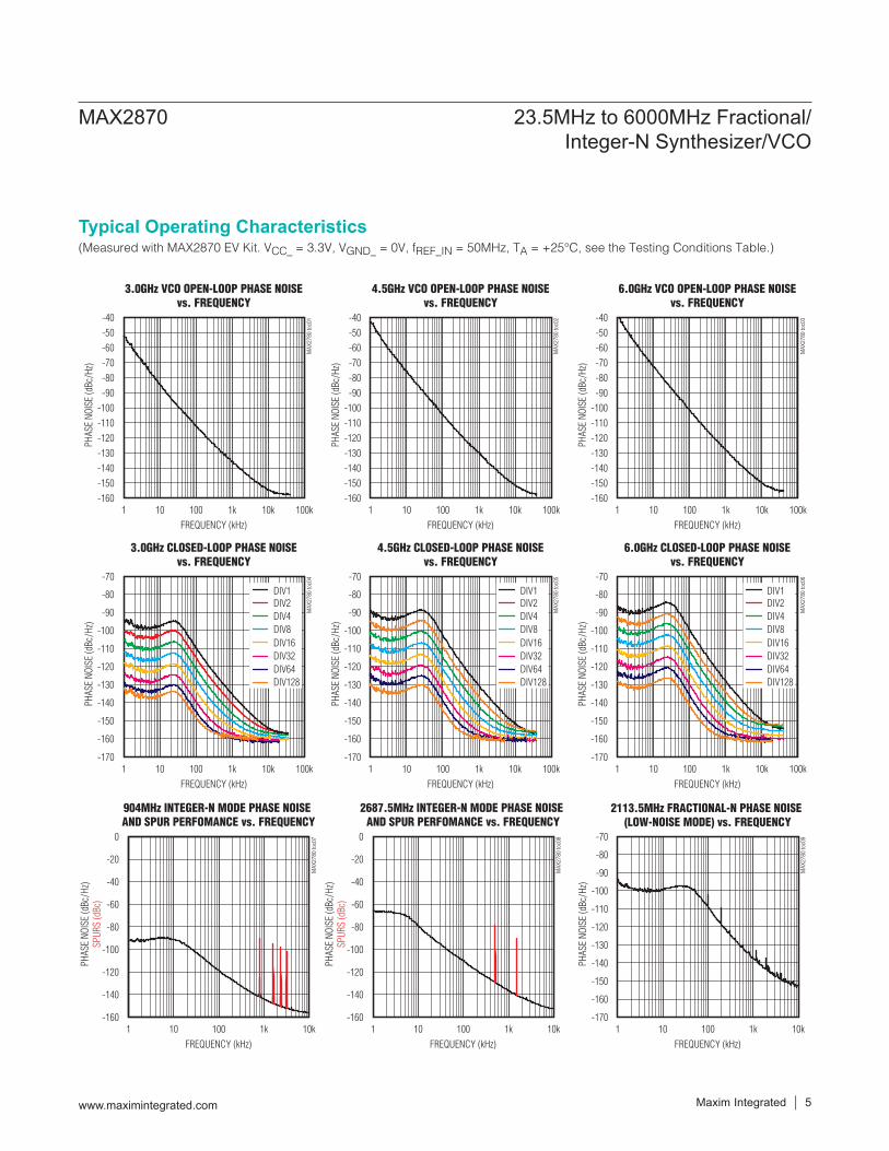
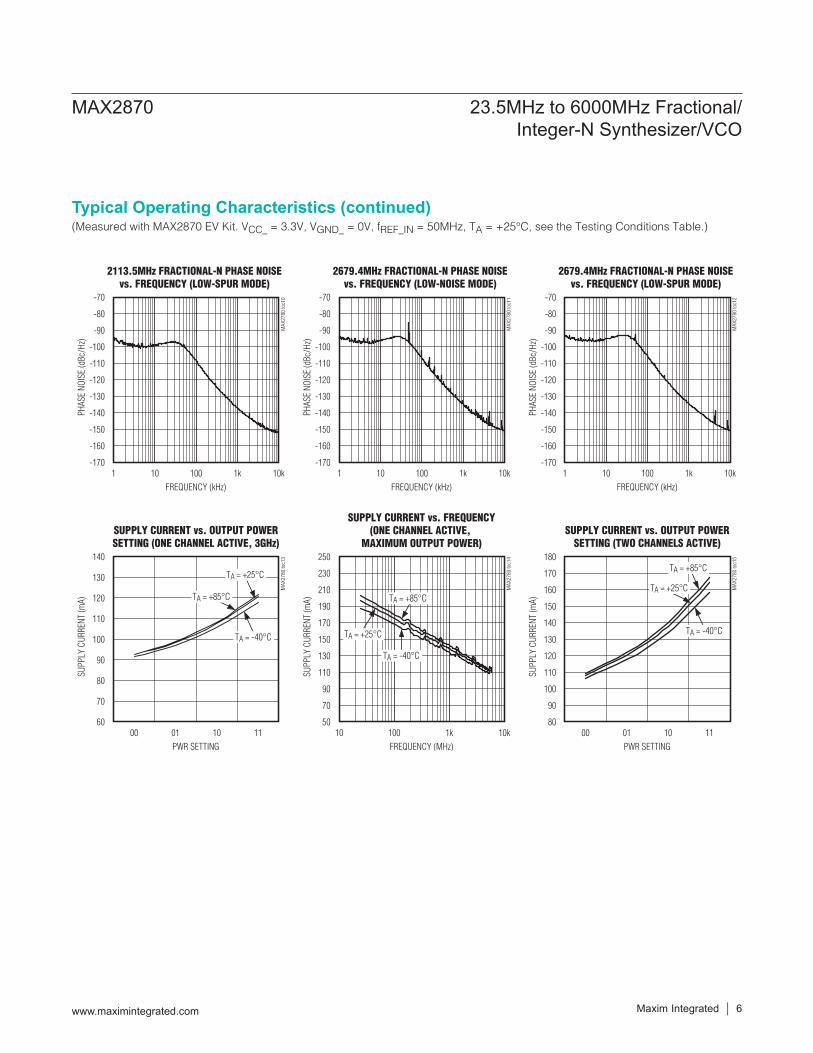
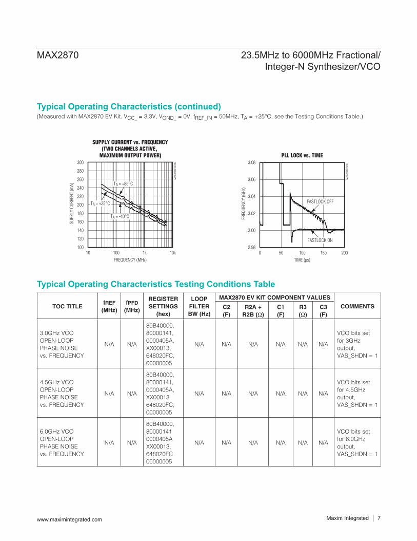
Typical Operating Characteristics(Measured with MAX2870 EV Kit. VCC_ = 3.3V, VGND_ = 0V, fREF_IN = 50MHz, TA = +25°C, see the Testing Conditions Table.)
MAX2870 23.5MHz to 6000MHz Fractional/ Integer-N Synthesizer/VCO
www.maximintegrated.com Maxim Integrated 5
3.0GHz VCO OPEN-LOOP PHASE NOISEvs. FREQUENCY
MAX
2780
toc0
1
FREQUENCY (kHz)
PHAS
E NO
ISE
(dBc
/Hz)
10k1k10010
-150
-140
-130
-120
-110
-100
-90
-80
-70
-60
-50
-40
-1601 100k
3.0GHz CLOSED-LOOP PHASE NOISEvs. FREQUENCY
MAX
2780
toc0
4
FREQUENCY (kHz)
PHAS
E NO
ISE
(dBc
/Hz)
10k1k10010
-70
-1701 100k
-160
-150
-140
-130
-120
-110
-100
-90
-80 DIV1DIV2DIV4DIV8DIV16DIV32DIV64DIV128
1k100101 10k
MAX
2780
toc0
7
FREQUENCY (kHz)
904MHz INTEGER-N MODE PHASE NOISE AND SPUR PERFOMANCE vs. FREQUENCY
0
-160
-140
-120
-100
-80
-60
-40
-20
PHAS
E NO
ISE
(dBc
/Hz)
SPUR
S (d
Bc)
4.5GHz VCO OPEN-LOOP PHASE NOISEvs. FREQUENCY
MAX
2780
toc0
2
FREQUENCY (kHz)
PHAS
E NO
ISE
(dBc
/Hz)
10k1k10010
-150
-140
-130
-120
-110
-100
-90
-80
-70
-60
-50
-40
-1601 100k
4.5GHz CLOSED-LOOP PHASE NOISEvs. FREQUENCY
MAX
2780
toc0
5
FREQUENCY (kHz)
PHAS
E NO
ISE
(dBc
/Hz)
10k1k10010
-70
-1701 100k
-160
-150
-140
-130
-120
-110
-100
-90
-80 DIV1DIV2DIV4DIV8DIV16DIV32DIV64DIV128
1k100101 10k
MAX
2780
toc0
8
FREQUENCY (kHz)
2687.5MHz INTEGER-N MODE PHASE NOISE AND SPUR PERFOMANCE vs. FREQUENCY
0
-160
-140
-120
-100
-80
-60
-40
-20
PHAS
E NO
ISE
(dBc
/Hz)
SPUR
S (d
Bc)
6.0GHz VCO OPEN-LOOP PHASE NOISEvs. FREQUENCY
MAX
2780
toc0
3
FREQUENCY (kHz)
PHAS
E NO
ISE
(dBc
/Hz)
10k1k10010
-150
-140
-130
-120
-110
-100
-90
-80
-70
-60
-50
-40
-1601 100k
6.0GHz CLOSED-LOOP PHASE NOISEvs. FREQUENCY
MAX
2780
toc0
6
FREQUENCY (kHz)
PHAS
E NO
ISE
(dBc
/Hz)
10k1k10010
-70
-1701 100k
-160
-150
-140
-130
-120
-110
-100
-90
-80 DIV1DIV2DIV4DIV8DIV16DIV32DIV64DIV128
1k100101 10k
2113.5MHz FRACTIONAL-N PHASE NOISE (LOW-NOISE MODE) vs. FREQUENCY
MAX
2780
toc0
9
FREQUENCY (kHz)
PHAS
E NO
ISE
(dBc
/Hz)
-160
-150
-140
-130
-120
-110
-100
-90
-80
-70
-170
Typical Operating Characteristics (continued)(Measured with MAX2870 EV Kit. VCC_ = 3.3V, VGND_ = 0V, fREF_IN = 50MHz, TA = +25°C, see the Testing Conditions Table.)
MAX2870 23.5MHz to 6000MHz Fractional/ Integer-N Synthesizer/VCO
www.maximintegrated.com Maxim Integrated 6
1k100101 10k
MAX
2780
toc1
0
FREQUENCY (kHz)
PHAS
E NO
ISE
(dBc
/Hz)
-160
-150
-140
-130
-120
-110
-100
-90
-80
-70
-170
2113.5MHz FRACTIONAL-N PHASE NOISEvs. FREQUENCY (LOW-SPUR MODE)
1k100101 10k
MAX
2780
toc1
1
FREQUENCY (kHz)
PHAS
E NO
ISE
(dBc
/Hz)
-160
-150
-140
-130
-120
-110
-100
-90
-80
-70
-170
2679.4MHz FRACTIONAL-N PHASE NOISEvs. FREQUENCY (LOW-NOISE MODE)
SUPPLY CURRENT vs. OUTPUT POWERSETTING (ONE CHANNEL ACTIVE, 3GHz)
MAX
2780
toc1
3
SUPP
LY C
URRE
NT (m
A)
70
80
90
100
110
120
130
140
60
PWR SETTING
00 01 10 11
TA = +25°C
TA = +85°C
TA = -40°C
1k100101 10k
MAX
2780
toc1
2
FREQUENCY (kHz)
PHAS
E NO
ISE
(dBc
/Hz)
-160
-150
-140
-130
-120
-110
-100
-90
-80
-70
-170
2679.4MHz FRACTIONAL-N PHASE NOISEvs. FREQUENCY (LOW-SPUR MODE)
SUPPLY CURRENT vs. FREQUENCY(ONE CHANNEL ACTIVE,
MAXIMUM OUTPUT POWER)
MAX
2780
toc1
4
FREQUENCY (MHz)
SUPP
LY C
URRE
NT (m
A)
1k100
70
90
110
130
150
170
190
210
230
250
5010 10k
TA = +25°C
TA = +85°C
TA = -40°C
SUPPLY CURRENT vs. OUTPUT POWERSETTING (TWO CHANNELS ACTIVE)
MAX
2780
toc1
5
SUPP
LY C
URRE
NT (m
A)
180
80
PWR SETTING
00 01 10 11
TA = +25°C
TA = +85°C
TA = -40°C
90
100
110
120
130
140
150
160
170
Typical Operating Characteristics (continued)(Measured with MAX2870 EV Kit. VCC_ = 3.3V, VGND_ = 0V, fREF_IN = 50MHz, TA = +25°C, see the Testing Conditions Table.)
Typical Operating Characteristics Testing Conditions Table
MAX2870 23.5MHz to 6000MHz Fractional/ Integer-N Synthesizer/VCO
www.maximintegrated.com Maxim Integrated 7
TOC TITLEfREF
(MHz)fPFD
(MHz)
REGISTER SETTINGS
(hex)
LOOP FILTER BW (Hz)
MAX2870 EV KIT COMPONENT VALUES
COMMENTSC2 (F)
R2A + R2B (I)
C1(F)
R3 (I)
C3 (F)
3.0GHz VCO OPEN-LOOP PHASE NOISEvs. FREQUENCY
N/A N/A
80B40000, 80000141, 0000405A, XX00013, 648020FC, 00000005
N/A N/A N/A N/A N/A N/A
VCO bits set for 3GHz output,VAS_SHDN = 1
4.5GHz VCO OPEN-LOOP PHASE NOISEvs. FREQUENCY
N/A N/A
80B40000, 80000141, 0000405A, XX00013 648020FC, 00000005
N/A N/A N/A N/A N/A N/A
VCO bits set for 4.5GHz output,VAS_SHDN = 1
6.0GHz VCO OPEN-LOOP PHASE NOISEvs. FREQUENCY
N/A N/A
80B40000, 80000141 0000405A XX00013, 648020FC 00000005
N/A N/A N/A N/A N/A N/A
VCO bits set for 6.0GHz output,VAS_SHDN = 1
SUPPLY CURRENT vs. FREQUENCY(TWO CHANNELS ACTIVE,
MAXIMUM OUTPUT POWER)
MAX
2780
toc1
6
FREQUENCY (MHz)
SUPP
LY C
URRE
NT (m
A)
1k100
120
140
160
180
200
220
240
260
280
300
10010 10k
TA = +25°C
TA = +85°C
TA = -40°C
PLL LOCK vs. TIME
MAX
2780
toc1
7
TIME (µs)
FREQ
UENC
Y (G
Hz)
15010050
3.00
3.02
3.04
3.06
3.08
2.980 200
FASTLOCK OFF
FASTLOCK ON
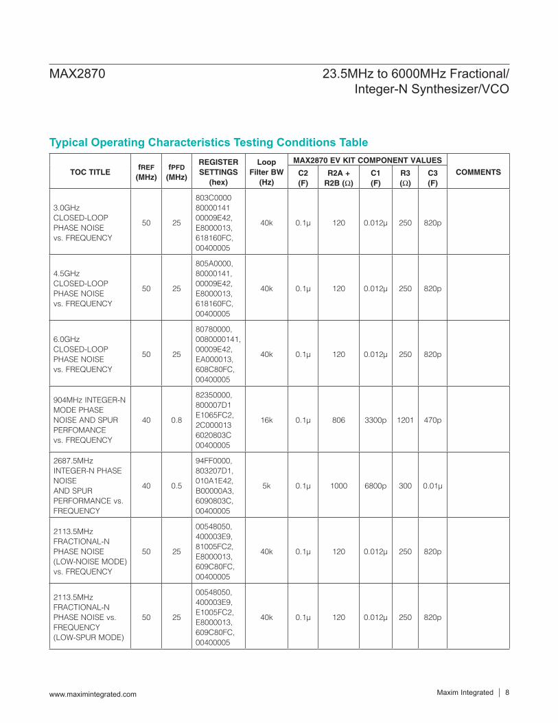
Typical Operating Characteristics Testing Conditions Table
MAX2870 23.5MHz to 6000MHz Fractional/ Integer-N Synthesizer/VCO
www.maximintegrated.com Maxim Integrated 8
TOC TITLEfREF
(MHz)fPFD
(MHz)
REGISTER SETTINGS
(hex)
Loop Filter BW
(Hz)
MAX2870 EV KIT COMPONENT VALUES
COMMENTSC2 (F)
R2A + R2B (I)
C1(F)
R3 (I)
C3 (F)
3.0GHz CLOSED-LOOP PHASE NOISEvs. FREQUENCY
50 25
803C0000 80000141 00009E42, E8000013, 618160FC, 00400005
40k 0.1F 120 0.012F 250 820p
4.5GHz CLOSED-LOOP PHASE NOISEvs. FREQUENCY
50 25
805A0000, 80000141, 00009E42, E8000013, 618160FC, 00400005
40k 0.1F 120 0.012F 250 820p
6.0GHz CLOSED-LOOP PHASE NOISEvs. FREQUENCY
50 25
80780000, 0080000141, 00009E42, EA000013, 608C80FC, 00400005
40k 0.1F 120 0.012F 250 820p
904MHz INTEGER-N MODE PHASE NOISE AND SPUR PERFOMANCEvs. FREQUENCY
40 0.8
82350000, 800007D1 E1065FC2, 2C000013 6020803C 00400005
16k 0.1F 806 3300p 1201 470p
2687.5MHz INTEGER-N PHASE NOISEAND SPUR PERFORMANCE vs. FREQUENCY
40 0.5
94FF0000, 803207D1, 010A1E42, B00000A3, 6090803C, 00400005
5k 0.1F 1000 6800p 300 0.01F
2113.5MHz FRACTIONAL-N PHASE NOISE(LOW-NOISE MODE) vs. FREQUENCY
50 25
00548050, 400003E9, 81005FC2, E8000013, 609C80FC, 00400005
40k 0.1F 120 0.012F 250 820p
2113.5MHz FRACTIONAL-N PHASE NOISE vs. FREQUENCY(LOW-SPUR MODE)
50 25
00548050, 400003E9, E1005FC2, E8000013, 609C80FC, 00400005
40k 0.1F 120 0.012F 250 820p

Typical Operating Characteristics Testing Conditions Table
MAX2870 23.5MHz to 6000MHz Fractional/ Integer-N Synthesizer/VCO
www.maximintegrated.com Maxim Integrated 9
TOC TITLEfREF
(MHz)fPFD
(MHz)
REGISTER SETTINGS
(hex)
Loop Filter BW
(Hz)
MAX2870 EV KIT COMPONENT VALUES
COMMENTSC2 (F)
R2A + R2B (I)
C1(F)
R3 (I)
C3 (F)
2679.4MHz FRACTIONAL-N PHASE NOISE vs. FREQUENCY(LOW-NOISE MODE)
50 25
00358160, 203207D1, 01005E42, B20000A3, 6010003C, 00400005
40k 0.1F 120 0.012F 250 820p
2679.4MHz FRACTIONAL-N PHASE NOISE vs. FREQUENCY(LOW-SPUR MODE)
50 25
00358160, 203207D1, 41005E42, B20000A3, 6010003C, 00400005
40k 0.1F 120 0.012F 250 820p
SUPPLY CURRENT vs. OUTPUT POWER SETTING(ONE CHANNEL ACTIVE, 3GHz)
50 25
003C0000, 20000321, 01005E42, 00000013, 610F423C, 01400005,
APWR swept from 00 to 11
SUPPLY CURRENT vs. FREQUENCY(ONE CHANNEL ACTIVE, MAXIMUM OUTPUT POWER)
50 25
003C0000, 20000321, 01005E42, 00000013, 610F423C, 01400005
N and F values changed for each frequency
SUPPLY CURRENT vs. OUTPUT POWER SETTING (TWO CHANNELS ACTIVE)
50 25
003C0000, 20000321, 01005E42, 00000013, 610F43FC, 01400005
APWR and BPWR swept from 00 to 11
SUPPLY CURRENT vs. FREQUENCY(TWO CHANNELS ACTIVE MAXIMUM OUTPUT POWER)
50 25
003C0000, 20000321, 01005E42, 00000013, 610F43FC, 01400005
N and F values swept for each frequency
PLL LOCK vs. TIME 40 40
00250120, 20320141, 00004042, 000000A3, 0184023C, 01400005
40k 0.1F 120 0.012F 250 820pCDM changed from 00 to 01

Pin Description
Pin Configuration
MAX2870 23.5MHz to 6000MHz Fractional/ Integer-N Synthesizer/VCO
www.maximintegrated.com Maxim Integrated 10
PIN NAME FUNCTION
1 CLKSerial Clock Input. The data is latched into the 32-bit shift register on the rising edge of the CLK line.
2 DATA Serial Data Input. The serial data is loaded MSB first. The 3 LSBs identify the register address.
3 LELoad Enable Input. When LE goes high the data stored in the shift register is loaded into the appropriate latches.
4 CEChip Enable. A logic-low powers the part down and the charge pump becomes high impedance.
5 SWFast-Lock Switch. Connect to the loop filter when using the fast-lock mode. No connect in Normal mode
6 VCC_CP Power Supply for Charge Pump. Place decoupling capacitors as close as possible to the pin.
7 CP_OUT Charge-Pump Output. Connect to external loop filter input.
8 GND_CP Ground for Charge-Pump. Connect to board ground, not to the paddle.
9 GND_PLL Ground for PLL. Connect to main board ground plane, not to the paddle.
10 VCC_PLL Power Supply for PLL. Place decoupling capacitors as close as possible to the pin.
11 GND_RF Ground for RF Outputs. Connect to board ground plane, not to the paddle.
12 RFOUTA_P Open Collector Positive RF Output A. Connect to supply through RF choke or 50I load.
MAX2870
TQFN
TOP VIEW
29
30
28
27
12
11
13
DATA CE SW
V CC_
CP
CP_O
UT
14
CLK
BIAS
_FIL
T
GND_
TUNE
TUNE
REG
NOIS
E_FI
LT
GND_
VCO
1 2
VCC_DIG
4 5 6 7
2324 22 20 19 18
REF_IN
MUX_OUT
RFOUTB_P
RFOUTA_N
RFOUTA_P
GND_RF
LERS
ET
3
21
31 10GND_SD EP VCC_PLL
32 9VDD_SD GND_PLL+
GND_DIG
26 15 RFOUTB_NRFOUT_EN
25 16 VCC_RF
GND_
CPV C
C_VC
O8
17
LD
Pin Description (continued)
MAX2870 23.5MHz to 6000MHz Fractional/ Integer-N Synthesizer/VCO
www.maximintegrated.com Maxim Integrated 11
PIN NAME FUNCTION
13 RFOUTA_N Open Collector Negative RF Output A. Connect to supply through RF choke or 50I load.
14 RFOUTB_P Open Collector Positive RF Output B. Connect to supply through RF choke or 50I load.
15 RFOUTB_N Open Collector Negative RF Output B. Connect to supply through RF choke or 50I load.
16 VCC_RFPower Supply for RF Output and Dividers. Place decoupling capacitors as close as possible to the pin.
17 VCC_VCO VCO Power Supply. Place decoupling capacitors to the analog ground plane.
18 GND_VCO Ground for VCO. Connect to main board ground plane, not directly to the paddle.
19 NOISE_FILT VCO Noise Decoupling. Place a 1FF capacitor to ground.
20 TUNE Control Input to the VCO. Connect to external loop filter.
21 GND_TUNEGround for Control Input to the VCO. Connect to main board ground plane, not directly to the paddle.
22 RSETCharge-Pump Current Range Input. Connect an external resistor to ground to set the minimum CP current. ICP = 1.63/RSET x (1 + CP)
23 BIAS_FILT VCO Noise Decoupling. Place a 1FF capacitor to ground.
24 REG Reference Voltage Compensation. Place a 1FF capacitor to ground.
25 LDLock Detect Output. Logic-high when locked, and logic-low when unlocked. See register description for more details (Table 9).
26 RFOUT_EN RF Output Enable. A logic-low disables the RF outputs.
27 GND_DIG Ground for Digital circuitry. Connect to main board ground plane, not directly to the paddle.
28 VCC_DIG Power Supply for Digital Circuitry. Place decoupling capacitors as close as possible to pin.
29 REF_INReference Frequency Input. This is a high-impedance input with a nominal bias voltage of VCC_DIG/2. AC-couple to reference signal.
30 MUX_OUT Multiplexed Output and Serial Data Out. See Table 6.
31 GND_SDGround for Sigma-Delta Modulator. Connect to main board ground plane, not directly to the paddle.
32 VCC_SDPower Supply for Sigma-Delta Modulator. Place decoupling capacitors as close as possible to the pin.
— EP Exposed Pad. Connect to board ground.
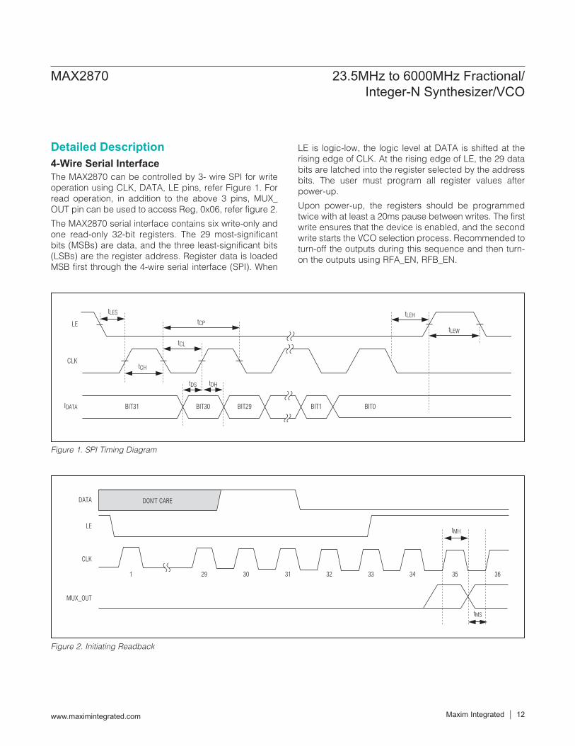
Detailed Description4-Wire Serial InterfaceThe MAX2870 can be controlled by 3- wire SPI for write operation using CLK, DATA, LE pins, refer Figure 1. For read operation, in addition to the above 3 pins, MUX_OUT pin can be used to access Reg, 0x06, refer figure 2.
The MAX2870 serial interface contains six write-only and one read-only 32-bit registers. The 29 most-significant bits (MSBs) are data, and the three least-significant bits (LSBs) are the register address. Register data is loaded MSB first through the 4-wire serial interface (SPI). When
LE is logic-low, the logic level at DATA is shifted at the rising edge of CLK. At the rising edge of LE, the 29 data bits are latched into the register selected by the address bits. The user must program all register values after power-up.
Upon power-up, the registers should be programmed twice with at least a 20ms pause between writes. The first write ensures that the device is enabled, and the second write starts the VCO selection process. Recommended to turn-off the outputs during this sequence and then turn-on the outputs using RFA_EN, RFB_EN.
Figure 1. SPI Timing Diagram
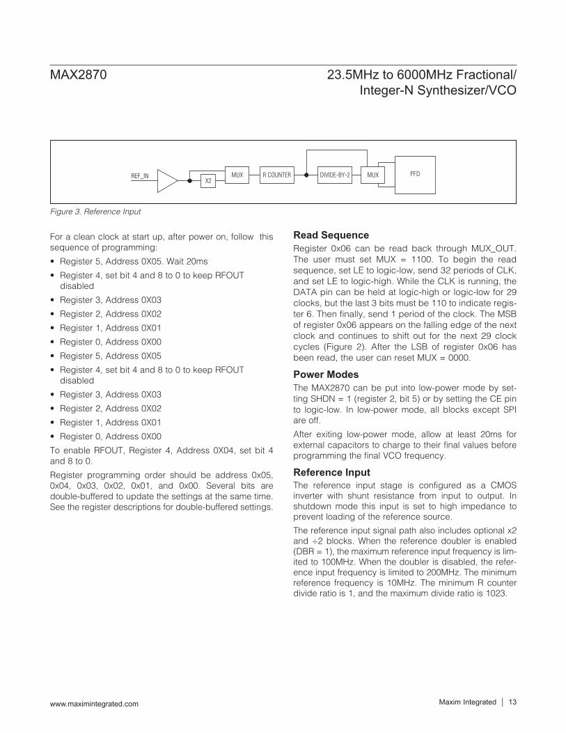
Figure 2. Initiating Readback
MAX2870 23.5MHz to 6000MHz Fractional/ Integer-N Synthesizer/VCO
www.maximintegrated.com Maxim Integrated 12
LE
CLK
32
DATA
3130291 33 34 35
tMS
tMH
36
DON’T CARE
MUX_OUT
LE
tDS tDH
tCL
tLEH
CLK
IDATA BIT31 BIT30 BIT29 BIT1 BIT0
tLES
tCH
tCPtLEW
For a clean clock at start up, after power on, follow this sequence of programming:
• Register 5, Address 0X05. Wait 20ms
• Register 4, set bit 4 and 8 to 0 to keep RFOUT disabled
• Register 3, Address 0X03
• Register 2, Address 0X02
• Register 1, Address 0X01
• Register 0, Address 0X00
• Register 5, Address 0X05
• Register 4, set bit 4 and 8 to 0 to keep RFOUT disabled
• Register 3, Address 0X03
• Register 2, Address 0X02
• Register 1, Address 0X01
• Register 0, Address 0X00
To enable RFOUT, Register 4, Address 0X04, set bit 4 and 8 to 0.
Register programming order should be address 0x05, 0x04, 0x03, 0x02, 0x01, and 0x00. Several bits are double-buffered to update the settings at the same time. See the register descriptions for double-buffered settings.
Read SequenceRegister 0x06 can be read back through MUX_OUT. The user must set MUX = 1100. To begin the read sequence, set LE to logic-low, send 32 periods of CLK, and set LE to logic-high. While the CLK is running, the DATA pin can be held at logic-high or logic-low for 29 clocks, but the last 3 bits must be 110 to indicate regis-ter 6. Then finally, send 1 period of the clock. The MSB of register 0x06 appears on the falling edge of the next clock and continues to shift out for the next 29 clock cycles (Figure 2). After the LSB of register 0x06 has been read, the user can reset MUX = 0000.
Power ModesThe MAX2870 can be put into low-power mode by set-ting SHDN = 1 (register 2, bit 5) or by setting the CE pin to logic-low. In low-power mode, all blocks except SPI are off.
After exiting low-power mode, allow at least 20ms for external capacitors to charge to their final values before programming the final VCO frequency.
Reference InputThe reference input stage is configured as a CMOS inverter with shunt resistance from input to output. In shutdown mode this input is set to high impedance to prevent loading of the reference source.
The reference input signal path also includes optional x2 and ÷2 blocks. When the reference doubler is enabled (DBR = 1), the maximum reference input frequency is lim-ited to 100MHz. When the doubler is disabled, the refer-ence input frequency is limited to 200MHz. The minimum reference frequency is 10MHz. The minimum R counter divide ratio is 1, and the maximum divide ratio is 1023.
Figure 3. Reference Input
MAX2870 23.5MHz to 6000MHz Fractional/ Integer-N Synthesizer/VCO
www.maximintegrated.com Maxim Integrated 13
REF_INX2
DIVIDE-BY-2 PFDR COUNTER MUXMUX
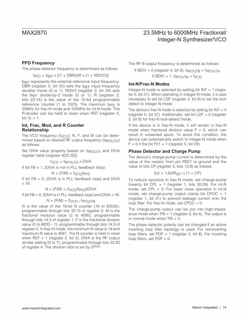
PFD FrequencyThe phase-detector frequency is determined as follows:
fPFD = fREF O [(1 + DBR)/(R x (1 + RDIV2))]
fREF represents the external reference input frequency. DBR (register 2, bit 25) sets the fREF input frequency doubler mode (0 or 1). RDIV2 (register 2, bit 24) sets the fREF divide-by-2 mode (0 or 1). R (register 2, bits 23:14) is the value of the 10-bit programmable reference counter (1 to 1023). The maximum fPFD is 50MHz for frac-N mode and 105MHz for int-N mode. The R-divider can be held in reset when RST (register 2, bit 3) = 1.
Int, Frac, Mod, and R Counter RelationshipThe VCO frequency (fVCO), N, F, and M can be deter-mined based on desired RF output frequency (fRFOUTA) as follows:
Set DIVA value property based on fRFOUTA and DIVA register table (register 4[22.20])
fVCO = fRFOUTA x DIVA
If bit FB = 1, (DIVA is not in PLL feedback loop):N + (F/M) = fVCO/fPFD
If bit FB = 0, (DIVA is in PLL feedback loop) and DIVA ≤ 16:
N + (F/M) = (fVCO/fPFD)/DIVAIf bit FB = 0, (DIVA is in PLL feedback loop) and DIVA > 16:
N + (F/M) = (fVCO / fPFD)/16N is the value of the 16-bit N counter (16 to 65535), programmable through bits 30:15 of register 0. M is the fractional modulus value (2 to 4095), programmable through bits 14:3 of register 1. F is the fractional division value (0 to MOD - 1), programmable through bits 14:3 of register 0. In frac-N mode, the minimum N value is 19 and maximum N value is 4091. The N counter is held in reset when RST = 1 (register 2, bit 3). DIVA is the RF output divider setting (0 to 7), programmable through bits 22:20 of register 4. The division ratio is set by 2DIVA.
The RF B output frequency is determined as follows:
If BDIV = 0 (register 4, bit 9), fRFOUTB = fRFOUTA.
If BDIV = 1, fRFOUTB = fVCO.
Int-N/Frac-N ModesInteger-N mode is selected by setting bit INT = 1 (regis-ter 0, bit 31). When operating in integer-N mode, it is also necessary to set bit LDF (register 2, bit 8) to set the lock detect to integer-N mode.
The device’s frac-N mode is selected by setting bit INT = 0 (register 0, bit 31). Additionally, set bit LDF = 0 (register 2, bit 8) for frac-N lock-detect mode.
If the device is in frac-N mode, it will remain in frac-N mode when fractional division value F = 0, which can result in unwanted spurs. To avoid this condition, the device can automatically switch to integer-N mode when F = 0 if the bit F01 = 1 (register 5, bit 24).
Phase Detector and Charge PumpThe device’s charge-pump current is determined by the value of the resistor from pin RSET to ground and the value of bits CP (register 2, bits 12:9) as follows:
ICP = 1.63/RSET x (1 + CP)
To reduce spurious in frac-N mode, set charge-pump linearity bit CPL = 1 (register 1, bits 30:29). For int-N mode, set CPL = 0. For lower noise operation in int-N mode, set charge-pump output clamp bit CPOC = 1 (register 1, bit 31) to prevent leakage current onto the loop filter. For frac-N mode, set CPOC = 0.
The charge-pump output can be put into high-imped-ance mode when TRI = 1 (register 2, bit 4). The output is in normal mode when TRI = 0.
The phase detector polarity can be changed if an active inverting loop filter topology is used. For noninverting loop filters, set PDP = 1 (register 2, bit 6). For inverting loop filters, set PDP = 0.
MAX2870 23.5MHz to 6000MHz Fractional/ Integer-N Synthesizer/VCO
www.maximintegrated.com Maxim Integrated 14

Table 2. Int-N Digital Lock-Detect Settings
Table 1. Frac-N Digital Lock-Detect Settings
MUX_OUT and Lock DetectMUX_OUT is a multipurpose test output for observing various internal functions of the MAX2870. MUX_OUT can also be configured as serial data output. Bits MUX (register 2, bit 28:26) are used to select the desired MUX_OUT signal (see Table 6).
Lock detect can be monitored through the LD output by setting the LD bits (register 5, bits 23:22). For digital lock detect, set LD = 01. The digital lock detect is dependent on the mode of the synthesizer. In frac-N mode set LDF = 0, and in int-N mode set LDF = 1. To set the accuracy of the digital lock detect, see Table 1 and Table 2.
Analog lock detect can be set with LD = 10. In this mode, LD is an open-drain output and requires an external pullup resistor of typical value, 10KΩ.
The lock detect output validity is dependent on many factors. The lock detect output is not valid during the VCO auto selection process. After the VCO auto selec-tion process has completed, the lock detect output is not valid until the TUNE voltage has settled. TUNE voltage settling time is dependent on loop filter bandwidth, and can be calculated using the EE-Sim Simulation tool found at www.maximintegrated.com.
Fast-LockThe device uses a fast-lock mode to decrease lock time. This mode requires that CP = 0000 (register 2, bits 12:9) and that the shunt resistive portion of the loop filter be segmented into two parts, where one resistor (R2A) is 1/4th the total resistance, and the other resistor (R2B) is
3/4th the total resistance. The larger resistor should be connected from SW to ground, and the smaller resistor from SW to the loop filter capacitor. When CDM = 01 (register 3, bits 16:15), fast-lock is active after the VAS has completed. During fast-lock, the charge pump is increased to CP = 1111 and the shunt loop filter resis-tance is set to 1/4th the total resistance by changing pin SW from high impedance to ground. Fast-lock deacti-vates after a timeout set by the user. This timeout is loop filter dependent, and is set by:
tFAST-LOCK = M x CDIV/fPFD
where M is the modulus setting and CDIV is the clock divider setting. The user must determine the CDIV setting based on their loop filter time constant. The SW pin can be left open/ no connect when fast lock mode is not used.
Figure 4. Fast Lock Filter Topology
MAX2870 23.5MHz to 6000MHz Fractional/ Integer-N Synthesizer/VCO
www.maximintegrated.com Maxim Integrated 15
PFD FREQUENCY LDS LDPLOCKED UP/DOWN
TIME SKEW (ns)NUMBER OF LOCKED CYCLES TO SET LD
UP/DOWNTIME SKEW TO UNSET LD (ns)
P 32MHz 0 0 10 5 15
P 32MHz 0 1 6 5 15
> 32MHz 1 X 4 5 4
PFD FREQUENCY LDS LDPLOCKED UP/DOWN
TIME SKEW (ns)NUMBER OF LOCKED CYCLES TO SET LD
UP/DOWNTIME SKEW TO UNSET LD (ns)
P 32MHz 0 0 10 40 15
P 32MHz 0 1 6 40 15
> 32MHz 1 X 4 40 4
C3 C2 C17 CP_OUT
R2A
R2B
R3
5 SW
MAX2870
20 TUNE
RFOUTA± and RFOUTB±The device has dual differential open-collector RF out-puts that require an external RF choke 50I resistor to supply for each output. Each differential output can be independently enabled or disabled by setting bits RFA_EN (register 4, bit 5) and RFB_EN (register 4, bit 8). Both outputs are also controlled by applying a logic-high (enabled) or logic-low (disabled) to pin RFOUT_EN.
The output power of each output can be individually controlled with APWR (register 4, bits 4:3) for RFOUTA and BPWR (register 4, bits 7:6) for RFOUTB. The avail-able differential output power settings are from -4dBm to +5dBm, in 3dB steps with 50I pullup to supply. The available single-ended output power ranges from -4dBm to +5dBm in 3dB steps with a RF choke to supply. Across the entire frequency range different pullup elements (L or R) are required for optimal output power. If the output is used single ended, the unused output should be termi-nated in a corresponding load.
Voltage-Controlled OscillatorThe fundamental VCO frequency of the device guarantees gap-free coverage from 3.0GHz to 6.0GHz using four individual VCO core blocks with 16 sub-bands within each block. Connect the output of the loop filter to the TUNE input. The TUNE input is used to control the VCO.
Tune ADCA 3-bit ADC is used to read the VCO tuning voltage. The ADC value can be read back by bits 22:20 in register 6. The ADC uses the ranges shown in Table 3.
Note that the digital or analog lock detect might still be valid when the tuning voltage is out of the compliance range.
VCO Autoselect (VAS) State MachineAn internal VCO autoselect state machine is initiated when register 0 is programmed to automatically select the correct VCO if bit VAS_SHDN = 0 (register 3, bit 25).
The state machine clock, fBS, must be set to 50kHz. This is set by the BS bits. The formula for setting BS is:
BS = fPFD/50kHz
where fPFD is the phase-detector frequency. The BS (regis-ter 4, bits 19:12) value should be rounded to the nearest integer. If the calculated BS is higher than 1023, then set
BS = 1023. If fPFD is lower than 50kHz, then set BS = 1. The time needed to select the correct VCO is 10/fBS.
The RETUNE (register 3, bit 24) bit is used to enable or disable the VAS auto-retune function. Should the 3-bit TUNE ADC detect that the VCO control voltage (VTUNE) has drifted into the 000 or 111 state, the VAS will initiate an auto-retune if RETUNE = 1. If RETUNE = 0, then this function is disabled.
If VAS_SHDN = 1, then the VCO can be manually selected by bits VCO (register 3, bits 31:26). Refer to the Applications Information section for detailed implementation of VCO manual selection.
Phase Shift ModeAfter achieving lock, the phase of the MAX2870 device’s RF output can be changed in increments of P/M x 360N. The absolute phase cannot be determined, but it can be changed relative to the current phase.
To change the phase, do the following:
1) Achieve lock at the desired frequency.
2) Set the increment of phase relative to the current phase by setting P = M x desired_phase_change/360N.
3) Enable the phase change by setting CDM = 10.
4) Reset CDM = 00.
Low-Spur ModeThe device offers three modes for the sigma-delta modu-lator. Low-noise mode offers lower in-band noise at the expense of spurs. The spurs can be reduced by setting SDN = 10 (register 2, bits 30:29) or SDN = 11 for different modes of dithering. The user can determine which mode works best for their application.
Table 3. ADC VCO Status
MAX2870 23.5MHz to 6000MHz Fractional/ Integer-N Synthesizer/VCO
www.maximintegrated.com Maxim Integrated 16
ADC VCO STATUS
000 Out-of-lock, VTUNE < 0.5V
001 In-lock, 0.5V < VTUNE < 0.7V
010 In-lock, 0.7V < VTUNE < 1.3V
011 Not used
100 Not used
101 In-lock, 1.3V < VTUNE < 2.1V
110 In-lock, 2.1V < VTUNE < 2.5V
111 Out-of-lock, VTUNE > 2.5V

Table 4. Register 0 (Address: 000, Default: 007D0000HEX)
Table 5. Register 1 (Address: 001, Default: 2000FFF9HEX)
Register and Bit DescriptionsThe operating mode of the device is controlled by six on-chip registers.
Defaults are not guaranteed upon power-up and are provided for reference only. All reserved bits should only be writ-ten with default values. In low-power mode, the register values are retained. Upon power-up, the registers should be programmed twice with at least a 20ms pause between writes. The first write ensures that the device is enabled, and the second write starts the VCO selection process.
MAX2870 23.5MHz to 6000MHz Fractional/ Integer-N Synthesizer/VCO
www.maximintegrated.com Maxim Integrated 17
BIT LOCATION BIT ID NAME DEFINITION
31 INTInt-N or Frac-N Mode Control
0 = Enables the fractional-N mode1 = Enables the integer-N modeThe LDF bit must also be set to the appropriate mode.
30:15 N[15:0]Integer Division
Value
Sets integer part (N-divider) of the feedback divider factor. All integer values from 16 to 65,535 are allowed for integer mode. Integer values from 19 to 4,091 are allowed for fractional mode.
14:3 FRAC[11:0]Fractional
Division Value
Sets fractional value:000000000000 = 0 (see F0I bit description)000000000001 = 1----111111111110 = 4094111111111111 = 4095
2:0 ADDR[2:0] Address Bits Register address bits 000
BIT LOCATION BIT ID NAME DEFINITION
31 CPOCCP Output
Clamp
Sets charge-pump output clamp mode.0 = Disables clamping of the CP output when the CP is off1 = Enables the clamping of the CP output when the CP is off (improved integer-N in-band phase noise)
30:29 CPL[1:0] CP Linearity
Sets CP linearity mode.00 = Disables the CP linearity mode (integer-N mode)01 = Enables the CP linearity mode (frac-N mode)10 = Reserved11 = Reserved
28:27 CPT[1:0]Charge Pump
Test
Sets charge-pump test modes.00 = Normal mode01 = Reserved10 = Force CP into source mode11 = Force CP into sink mode
26:15 P[11:0] Phase Value
Sets phase value. See the Phase Shift Mode section.000000000000 = 0000000000001 = 1 (recommended)-----111111111111 = 4095

Table 6. Register 2 (Address: 010, Default: 00004042HEX)
Table 5. Register 1 (Address: 001, Default: 2000FFF9HEX) (continued)
MAX2870 23.5MHz to 6000MHz Fractional/ Integer-N Synthesizer/VCO
www.maximintegrated.com Maxim Integrated 18
BIT LOCATION BIT ID NAME DEFINITION
31 LDSLock-Detect
Speed
Lock-detect speed adjustment.0 = fPFD P 32MHz1 = fPFD > 32MHz
30:29 SDN[1:0]Frac-N Noise
Mode
Sets noise mode (See the Low-Spur Mode section.)00 = Low-noise mode01 = Reserved10 = Low-spur mode 111 = Low-spur mode 2
28:26 MUX[3:0]MUX_OUT
Configuration
Sets MUX_OUT pin configuration (MSB bit located register 05).0000 = Three-state output0001 = D_VDD0010 = D_GND0011 = R-divider output0100 = N-divider output/20101 = Analog lock detect0110 = Digital lock detect0111:1011 = Reserved1100 = Read register 06 MUX_OUT is configured as serial data out.1101:1111 = Reserved
25 DBRReference
Doubler Mode
Sets reference doubler mode.0 = Disable reference doubler1 = Enable reference doubler
24 RDIV2Reference Div2
Mode
Sets reference divider mode.0 = Disable reference divide-by-21 = Enable reference divide-by-2
23:14 R[9:0]Reference
Divider Mode
Sets reference divide value (R). Double buffered by register 0.0000000000 = 0 (unused)0000000001 = 1-----1111111111 = 1023
BIT LOCATION BIT ID NAME DEFINITION
14:3 M[11:0]Modulus Value
(M)
Fractional modulus value used to program fVCO. See the Int, Frac, Mod, and R Counter Relationship section. Double buffered by register 0.000000000000 = Unused000000000001 = Unused000000000010 = 2-----111111111111 = 4095
2:0 ADDR[2:0] Address Bits Register address bits 001
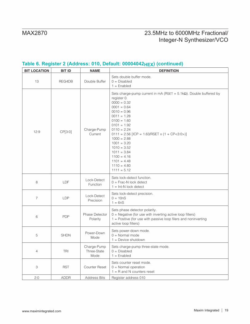
Table 6. Register 2 (Address: 010, Default: 00004042HEX) (continued)
MAX2870 23.5MHz to 6000MHz Fractional/ Integer-N Synthesizer/VCO
www.maximintegrated.com Maxim Integrated 19
BIT LOCATION BIT ID NAME DEFINITION
13 REG4DB Double BufferSets double buffer mode.0 = Disabled1 = Enabled
12:9 CP[3:0]Charge-Pump
Current
Sets charge-pump current in mA (RSET = 5.1kI). Double buffered by register 0.0000 = 0.320001 = 0.640010 = 0.960011 = 1.280100 = 1.600101 = 1.920110 = 2.240111 = 2.56 [ICP = 1.63/RSET x (1 + CP<3:0>)]1000 = 2.881001 = 3.201010 = 3.521011 = 3.841100 = 4.161101 = 4.481110 = 4.801111 = 5.12
8 LDFLock-Detect
Function
Sets lock-detect function.0 = Frac-N lock detect1 = Int-N lock detect
7 LDPLock-Detect
Precision
Sets lock-detect precision.0 = 10nS1 = 6nS
6 PDPPhase Detector
Polarity
Sets phase detector polarity.0 = Negative (for use with inverting active loop filters)1 = Positive (for use with passive loop filers and noninverting active loop filters)
5 SHDNPower-Down
Mode
Sets power-down mode.0 = Normal mode1 = Device shutdown
4 TRICharge-Pump Three-State
Mode
Sets charge-pump three-state mode.0 = Disabled1 = Enabled
3 RST Counter ResetSets counter reset mode.0 = Normal operation1 = R and N counters reset
2:0 ADDR Address Bits Register address 010
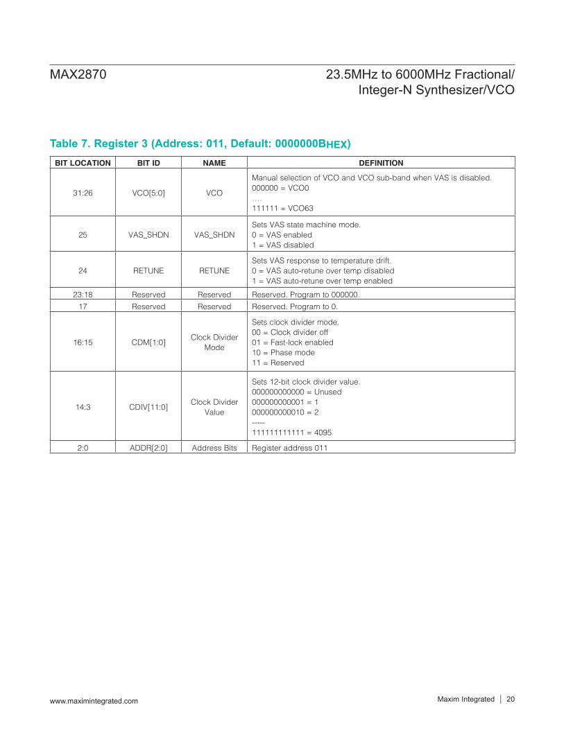
Table 7. Register 3 (Address: 011, Default: 0000000BHEX)
MAX2870 23.5MHz to 6000MHz Fractional/ Integer-N Synthesizer/VCO
www.maximintegrated.com Maxim Integrated 20
BIT LOCATION BIT ID NAME DEFINITION
31:26 VCO[5:0] VCO
Manual selection of VCO and VCO sub-band when VAS is disabled.000000 = VCO0….111111 = VCO63
25 VAS_SHDN VAS_SHDNSets VAS state machine mode.0 = VAS enabled1 = VAS disabled
24 RETUNE RETUNESets VAS response to temperature drift.0 = VAS auto-retune over temp disabled1 = VAS auto-retune over temp enabled
23:18 Reserved Reserved Reserved. Program to 000000.
17 Reserved Reserved Reserved. Program to 0.
16:15 CDM[1:0]Clock Divider
Mode
Sets clock divider mode.00 = Clock divider off01 = Fast-lock enabled10 = Phase mode11 = Reserved
14:3 CDIV[11:0]Clock Divider
Value
Sets 12-bit clock divider value.000000000000 = Unused000000000001 = 1000000000010 = 2-----111111111111 = 4095
2:0 ADDR[2:0] Address Bits Register address 011
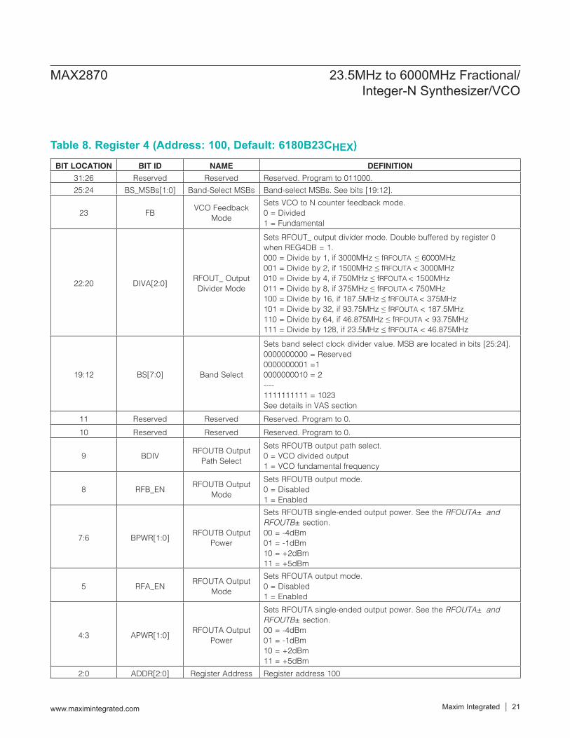
Table 8. Register 4 (Address: 100, Default: 6180B23CHEX)
MAX2870 23.5MHz to 6000MHz Fractional/ Integer-N Synthesizer/VCO
www.maximintegrated.com Maxim Integrated 21
BIT LOCATION BIT ID NAME DEFINITION
31:26 Reserved Reserved Reserved. Program to 011000.
25:24 BS_MSBs[1:0] Band-Select MSBs Band-select MSBs. See bits [19:12].
23 FBVCO Feedback
Mode
Sets VCO to N counter feedback mode.0 = Divided 1 = Fundamental
22:20 DIVA[2:0]RFOUT_ Output
Divider Mode
Sets RFOUT_ output divider mode. Double buffered by register 0 when REG4DB = 1.000 = Divide by 1, if 3000MHz ≤ fRFOUTA ≤ 6000MHz 001 = Divide by 2, if 1500MHz ≤ fRFOUTA < 3000MHz010 = Divide by 4, if 750MHz ≤ fRFOUTA < 1500MHz011 = Divide by 8, if 375MHz ≤ fRFOUTA < 750MHz100 = Divide by 16, if 187.5MHz ≤ fRFOUTA < 375MHz101 = Divide by 32, if 93.75MHz ≤ fRFOUTA < 187.5MHz110 = Divide by 64, if 46.875MHz ≤ fRFOUTA < 93.75MHz111 = Divide by 128, if 23.5MHz ≤ fRFOUTA < 46.875MHz
19:12 BS[7:0] Band Select
Sets band select clock divider value. MSB are located in bits [25:24].0000000000 = Reserved0000000001 =10000000010 = 2----1111111111 = 1023See details in VAS section
11 Reserved Reserved Reserved. Program to 0.
10 Reserved Reserved Reserved. Program to 0.
9 BDIVRFOUTB Output
Path Select
Sets RFOUTB output path select.0 = VCO divided output1 = VCO fundamental frequency
8 RFB_ENRFOUTB Output
Mode
Sets RFOUTB output mode.0 = Disabled1 = Enabled
7:6 BPWR[1:0]RFOUTB Output
Power
Sets RFOUTB single-ended output power. See the RFOUTAQ and RFOUTBQ section.00 = -4dBm01 = -1dBm10 = +2dBm11 = +5dBm
5 RFA_ENRFOUTA Output
Mode
Sets RFOUTA output mode.0 = Disabled1 = Enabled
4:3 APWR[1:0]RFOUTA Output
Power
Sets RFOUTA single-ended output power. See the RFOUTAQ and RFOUTBQ section.00 = -4dBm01 = -1dBm10 = +2dBm11 = +5dBm
2:0 ADDR[2:0] Register Address Register address 100
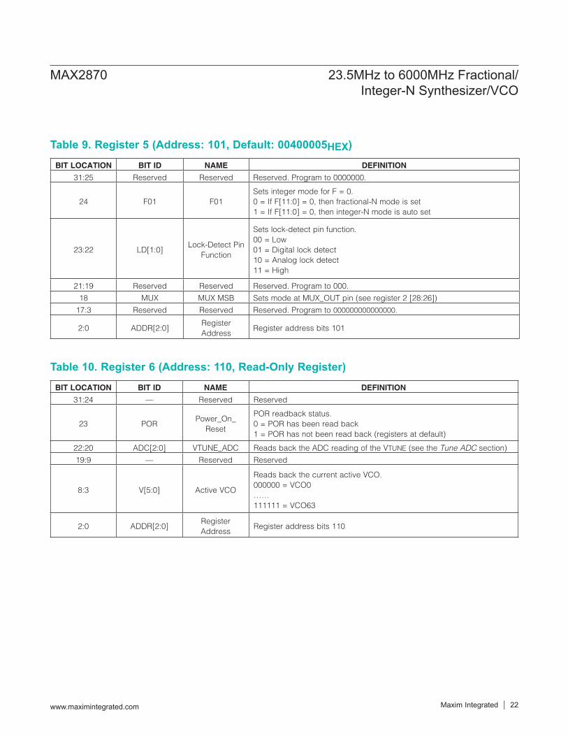
Table 9. Register 5 (Address: 101, Default: 00400005HEX)
Table 10. Register 6 (Address: 110, Read-Only Register)
MAX2870 23.5MHz to 6000MHz Fractional/ Integer-N Synthesizer/VCO
www.maximintegrated.com Maxim Integrated 22
BIT LOCATION BIT ID NAME DEFINITION
31:25 Reserved Reserved Reserved. Program to 0000000.
24 F01 F01Sets integer mode for F = 0.0 = If F[11:0] = 0, then fractional-N mode is set1 = If F[11:0] = 0, then integer-N mode is auto set
23:22 LD[1:0]Lock-Detect Pin
Function
Sets lock-detect pin function.00 = Low01 = Digital lock detect10 = Analog lock detect11 = High
21:19 Reserved Reserved Reserved. Program to 000.
18 MUX MUX MSB Sets mode at MUX_OUT pin (see register 2 [28:26])
17:3 Reserved Reserved Reserved. Program to 000000000000000.
2:0 ADDR[2:0]Register Address
Register address bits 101
BIT LOCATION BIT ID NAME DEFINITION
31:24 — Reserved Reserved
23 PORPower_On_
Reset
POR readback status.0 = POR has been read back1 = POR has not been read back (registers at default)
22:20 ADC[2:0] VTUNE_ADC Reads back the ADC reading of the VTUNE (see the Tune ADC section)
19:9 — Reserved Reserved
8:3 V[5:0] Active VCO
Reads back the current active VCO.000000 = VCO0……111111 = VCO63
2:0 ADDR[2:0]Register Address
Register address bits 110

Typical Application Circuit
MAX2870 23.5MHz to 6000MHz Fractional/ Integer-N Synthesizer/VCO
www.maximintegrated.com Maxim Integrated 23
FOR BEST PERFORMANCE GENERATETHREE SUPPLIES USING SEPARATE LDOSVCC_RFVCC_DIGVCC_PLL
1 2 3 4 5 6 7 8
VCC_DIG
REF_IN
MUX_OUT
EP
9
10
11
VDD_SD
GND_DIG
GND_SD
RFOUT_EN
24 23 22 21 20 19 18 17
LDTO GPIO
FROM GPIO
CLK
DA
TA LE CE SW
V CC_
CP
CP_O
UT
GN
D_C
P
GND_PLL
GND_RF
RFOUTA_P
RFOUTA_N
RFOUTA
RFOUTB
RFOUTB_P
RFOUTB_N
VCC_RF
V CC_
VCO
SPIINTERFACE
VCC_PLL
VCC_PLL
VCC_RF
VCC_PLL
VCC_RF
VCC_DIG
VCC_RF
VCC_DIG
GN
D_V
CO
GN
D_T
UN
E
RSET
NO
ISE_
FILT
BIA
S_FI
LT
REG
TUN
E
12
13
14
15
16
32
31
30
29
28
27
26
25
MAX2870
FROMGPIO
C1 C3C2
R2A
R2B
R3
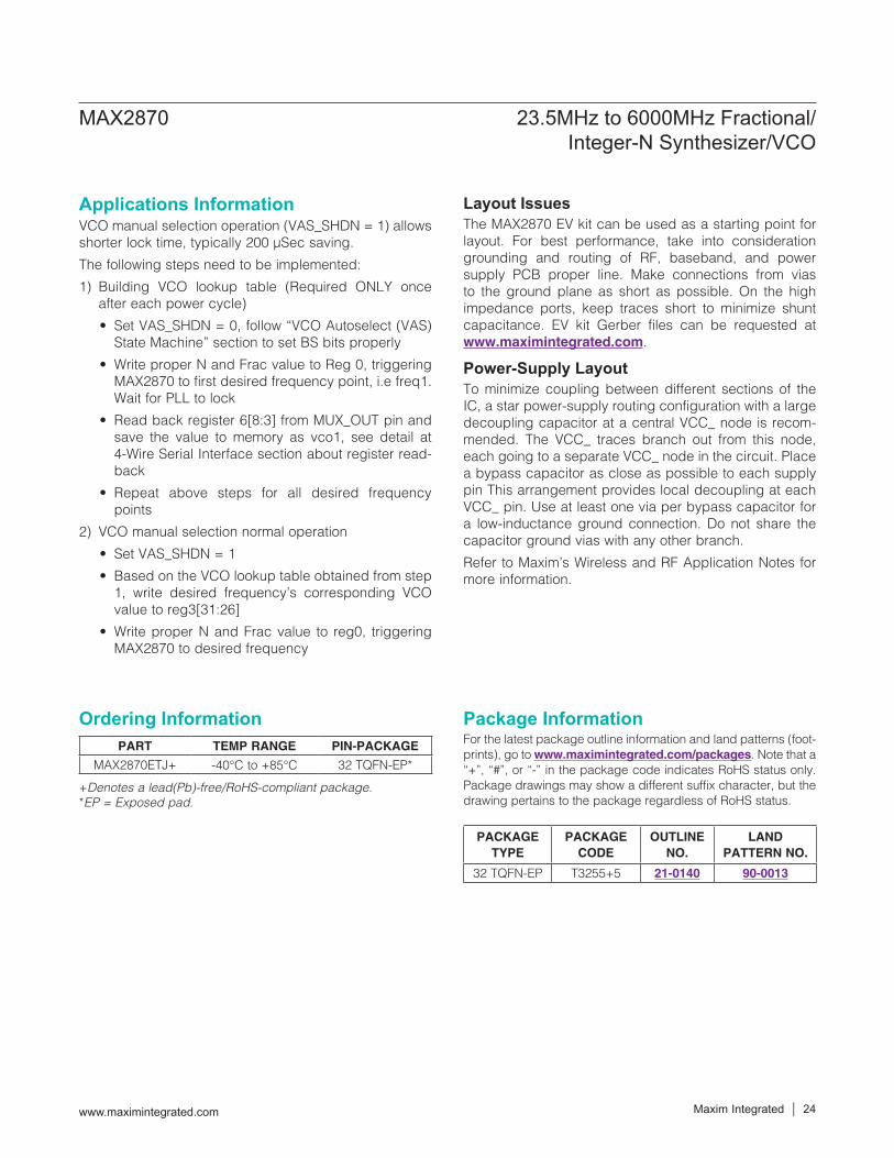
Ordering Information
+Denotes a lead(Pb)-free/RoHS-compliant package.*EP = Exposed pad.
Package InformationFor the latest package outline information and land patterns (foot-prints), go to www.maximintegrated.com/packages. Note that a “+”, “#”, or “-” in the package code indicates RoHS status only. Package drawings may show a different suffix character, but the drawing pertains to the package regardless of RoHS status.
Applications InformationVCO manual selection operation (VAS_SHDN = 1) allows shorter lock time, typically 200 µSec saving.
The following steps need to be implemented:
1) Building VCO lookup table (Required ONLY once after each power cycle)
• Set VAS_SHDN = 0, follow “VCO Autoselect (VAS) State Machine” section to set BS bits properly
• Write proper N and Frac value to Reg 0, triggering MAX2870 to first desired frequency point, i.e freq1. Wait for PLL to lock
• Read back register 6[8:3] from MUX_OUT pin and save the value to memory as vco1, see detail at 4-Wire Serial Interface section about register read-back
• Repeat above steps for all desired frequency points
2) VCO manual selection normal operation
• Set VAS_SHDN = 1
• Based on the VCO lookup table obtained from step 1, write desired frequency’s corresponding VCO value to reg3[31:26]
• Write proper N and Frac value to reg0, triggering MAX2870 to desired frequency
Layout IssuesThe MAX2870 EV kit can be used as a starting point for layout. For best performance, take into consideration grounding and routing of RF, baseband, and power supply PCB proper line. Make connections from vias to the ground plane as short as possible. On the high impedance ports, keep traces short to minimize shunt capacitance. EV kit Gerber files can be requested at www.maximintegrated.com.
Power-Supply LayoutTo minimize coupling between different sections of the IC, a star power-supply routing configuration with a large decoupling capacitor at a central VCC_ node is recom-mended. The VCC_ traces branch out from this node, each going to a separate VCC_ node in the circuit. Place a bypass capacitor as close as possible to each supply pin This arrangement provides local decoupling at each VCC_ pin. Use at least one via per bypass capacitor for a low-inductance ground connection. Do not share the capacitor ground vias with any other branch.
Refer to Maxim’s Wireless and RF Application Notes for more information.
MAX2870 23.5MHz to 6000MHz Fractional/ Integer-N Synthesizer/VCO
www.maximintegrated.com Maxim Integrated 24
PACKAGE TYPE
PACKAGE CODE
OUTLINE NO.
LAND PATTERN NO.
32 TQFN-EP T3255+5 21-0140 90-0013
PART TEMP RANGE PIN-PACKAGE
MAX2870ETJ+ -40NC to +85NC 32 TQFN-EP*
Revision History
Maxim Integrated cannot assume responsibility for use of any circuitry other than circuitry entirely embodied in a Maxim Integrated product. No circuit patent licenses are implied. Maxim Integrated reserves the right to change the circuitry and specifications without notice at any time. The parametric values (min and max limits) shown in the Electrical Characteristics table are guaranteed. Other parametric values quoted in this data sheet are provided for guidance.
Maxim Integrated and the Maxim Integrated logo are trademarks of Maxim Integrated Products, Inc. © 2017 Maxim Integrated Products, Inc. 25
MAX2870 23.5MHz to 6000MHz Fractional/ Integer-N Synthesizer/VCO
REVISIONNUMBER
REVISIONDATE
DESCRIPTIONPAGES
CHANGED
0 4/12 Initial release —
1 7/12 Updated Int, Frac, Mod and R Counter Relationship section; updated formula in VCO Autoselect (VAS) State Machine section, updated Table 8
13, 15, 20
2 11/12Updated Applications section, Note 3, Typical Operating Characteristics Testing Conditions Table, and Figure 1
1, 4, 7, 12
3 4/13Updated AC Electrical Characteristics table; updated SPI Characteristics, Pin Description, Fast-Lock, and VCO Autoselect State Machine sections. Replaced Figure 2
3, 4, 11, 12, 14
4 8/13 Updated Fast-Lock Section and Digital I/O Characteristics table 4, 14
5 3/14Updated the Four-Wire Serial Interface, MUX_OUT and Lock Detect, Register and Bit Descriptions sections, and Table 9
12–16, 21
6 4/17 Added VCO Manual Selection section and other general updates/corrections 1–3, 7–10, 12–24
For pricing, delivery, and ordering information, please contact Maxim Direct at 1-888-629-4642, or visit Maxim Integrated’s website at www.maximintegrated.com.