pe44820 evaluation kit user’s manualevaluation board assembly overview ... (evk) user’s manual...
TRANSCRIPT

DOC-72748-2 – (02/2017) EVK User’s Manualwww.psemi.com
PE29100 Evaluation Kit (EVK) User’s ManualUltraCMOS® High-speed FET Driver, 33 MHz
PE29100 Evaluation Kit

PE29100EVK User’s Manual
Page ii DOC-72748-2 – (02/2017)www.psemi.com
Copyright and Trademarks©2016-2017, Peregrine Semiconductor Corporation. All rights reserved. The Peregrine name, logo, UTSi and UltraCMOS are registered trademarks and HaRP, MultiSwitch and DuNE are trademarks of Peregrine Semicon-ductor Corp. eGaN is a registered trademark of Efficient Power Conversion Corporation, Inc. All other trade-marks mentioned herein are the property of their respective owners.
DisclaimersThe information in this document is believed to be reliable. However, Peregrine assumes no liability for the use of this information. Use shall be entirely at the user’s own risk. No patent rights or licenses to any circuits described in this document are implied or granted to any third party. Peregrine’s products are not designed or intended for use in devices or systems intended for surgical implant, or in other applications intended to support or sustain life, or in any application in which the failure of the Peregrine product could create a situation in which personal injury or death might occur. Peregrine assumes no liability for damages, including consequential or incidental damages, arising out of the use of its products in such applications.
Patent StatementPeregrine products are protected under one or more of the following U.S. patents: patents.psemi.com
Sales ContactFor additional information, contact Sales at [email protected].
Corporate Headquarters 9369 Carroll Park Drive, San Diego, CA, 92121
858-731-9400

PE29100EVK User’s Manual
Table of Contents
Introduction - - - - - - - - - - - - - - - - - - - - - - - - - - - - - - - - - - - - - - - - - - - - - - - - - - - - - - 1Introduction - - - - - - - - - - - - - - - - - - - - - - - - - - - - - - - - - - - - - - - - - - - - - - - - - - - - - - - - - - - - - - - - - - - - - - 1
Application Support . . . . . . . . . . . . . . . . . . . . . . . . . . . . . . . . . . . . . . . . . . . . . . . . . . . . . . . . . . . . . . . . . . . . . . . . . . . . . . . . . . 1Evaluation Kit Contents and Requirements . . . . . . . . . . . . . . . . . . . . . . . . . . . . . . . . . . . . . . . . . . . . . . . . . . . . . . . . . . . . . 1
Kit Contents . . . . . . . . . . . . . . . . . . . . . . . . . . . . . . . . . . . . . . . . . . . . . . . . . . . . . . . . . . . . . . . . . . . . . . . . . . . . . . . . . . . . . . . . . . . . . . . . . . . . 1Hardware Requirements . . . . . . . . . . . . . . . . . . . . . . . . . . . . . . . . . . . . . . . . . . . . . . . . . . . . . . . . . . . . . . . . . . . . . . . . . . . . . . . . . . . . . . . . . 2
Safety Precautions . . . . . . . . . . . . . . . . . . . . . . . . . . . . . . . . . . . . . . . . . . . . . . . . . . . . . . . . . . . . . . . . . . . . . . . . . . . . . . . . . . . . 2
Evaluation Board Assembly - - - - - - - - - - - - - - - - - - - - - - - - - - - - - - - - - - - - - - - - - - 3Evaluation Board Assembly Overview - - - - - - - - - - - - - - - - - - - - - - - - - - - - - - - - - - - - - - - - - - - - - - - - - - 3
Block Diagram and Schematic . . . . . . . . . . . . . . . . . . . . . . . . . . . . . . . . . . . . . . . . . . . . . . . . . . . . . . . . . . . . . . . . . . . . . . . . . 4Circuit Description . . . . . . . . . . . . . . . . . . . . . . . . . . . . . . . . . . . . . . . . . . . . . . . . . . . . . . . . . . . . . . . . . . . . . . . . . . . . . . . . . . . . 6
Quick Start Guide - - - - - - - - - - - - - - - - - - - - - - - - - - - - - - - - - - - - - - - - - - - - - - - - - 7Quick Start Overview - - - - - - - - - - - - - - - - - - - - - - - - - - - - - - - - - - - - - - - - - - - - - - - - - - - - - - - - - - - - - - - 7
Evaluation Board Overview . . . . . . . . . . . . . . . . . . . . . . . . . . . . . . . . . . . . . . . . . . . . . . . . . . . . . . . . . . . . . . . . . . . . . . . . . . . . 7Evaluation Test Setup . . . . . . . . . . . . . . . . . . . . . . . . . . . . . . . . . . . . . . . . . . . . . . . . . . . . . . . . . . . . . . . . . . . . . . . . . . . . . . . . . . . . . . . . . . . 9Hardware Operation . . . . . . . . . . . . . . . . . . . . . . . . . . . . . . . . . . . . . . . . . . . . . . . . . . . . . . . . . . . . . . . . . . . . . . . . . . . . . . . . . . . . . . . . . . . 10Thermal Considerations . . . . . . . . . . . . . . . . . . . . . . . . . . . . . . . . . . . . . . . . . . . . . . . . . . . . . . . . . . . . . . . . . . . . . . . . . . . . . . . . . . . . . . . . 12
Technical Resources - - - - - - - - - - - - - - - - - - - - - - - - - - - - - - - - - - - - - - - - - - - - - - - 13Technical Resources - - - - - - - - - - - - - - - - - - - - - - - - - - - - - - - - - - - - - - - - - - - - - - - - - - - - - - - - - - - - - - - 13
DOC-72748-2 – (02/2017) Page iiiwww.psemi.com

PE29100EVK User’s Manual
This page intentionally left blank.
Page iv DOC-72748-2 – (02/2017)www.psemi.com

1
PE29100EVK User’s Manual
Introduction
IntroductionThe PE29100 evaluation board allows the user to evaluate the PE29100 gate driver in a half-bridge configu-ration. The PE29100 integrated high-speed driver is designated to control the gates of external power devices, such as enhancement mode gallium nitride (eGaN®) FETs. The outputs of the PE29100 are capable of providing switching transition speeds in the sub nano-second range for hard switching applications up to 33 MHz.
The PE29100 evaluation kit (EVK) user’s manual includes the evaluation board schematic, circuit description, quick start guide, measurement results and a Bill of Materials (BoM).
Application SupportFor any technical inquiries regarding the evaluation kit or software, please visit applications support at www.psemi.com (fastest response) or call (858) 731-9400.
Evaluation Kit Contents and RequirementsKit Contents
The PE29100 EVK includes the following hardware required to evaluate the FET driver.
Table 1 • PE29100 Evaluation Kit Contents
Quality Description
1 PE29100 FET driver evaluation board assembly (PRT-66476)
DOC-72748-2 – (02/2017) Page 1www.psemi.com

PE29100EVK User’s Manual
Hardware RequirementsIn order to evaluate the performance of the evaluation board, the following equipment is required:
• High speed digital oscilloscope
• Functional generator (PWM)
• High voltage DC power supply
• DC power supply
• DC test leads
Safety PrecautionsCaution: The PE29100 FET driver EVK contains components that might be damaged by exposure to voltages in excess of the specified voltage, including voltages produced by electrostatic discharges. Handle the board in accordance with procedures for handling static-sensitive components. Avoid applying excessive voltages to the power supply terminals or signal inputs or outputs.
Caution: PCB surface can become hot. Contact may cause burns do not touch!
Page 2 DOC-72748-2 – (02/2017)www.psemi.com
2
PE29100EVK User’s Manual
Evaluation Board Assembly
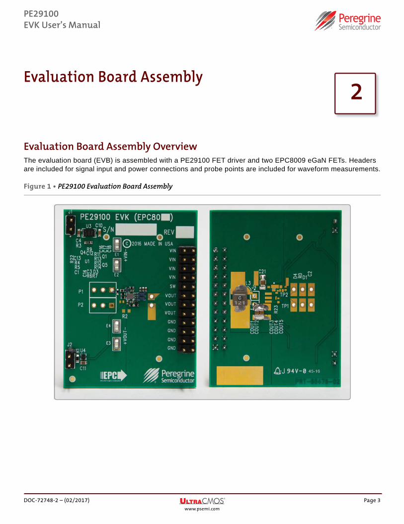
Evaluation Board Assembly OverviewThe evaluation board (EVB) is assembled with a PE29100 FET driver and two EPC8009 eGaN FETs. Headers are included for signal input and power connections and probe points are included for waveform measurements.
Figure 1 • PE29100 Evaluation Board Assembly
DOC-72748-2 – (02/2017) Page 3www.psemi.com

PE29100EVK User’s Manual
Block Diagram and SchematicThe block diagram and schematic of the evaluation board are shown in Figure 2 and Figure 3.
Figure 2 • PE29100 Evaluation Board Block Diagram
Page 4 DOC-72748-2 – (02/2017)www.psemi.com
PE29100EVK User’s Manual
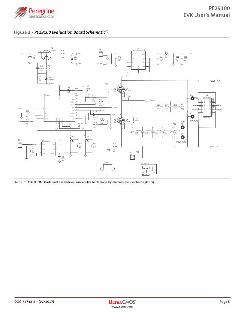
Figure 3 • PE29100 Evaluation Board Schematic(*)
Note: * CAUTION: Parts and assemblies susceptible to damage by electrostatic discharge (ESD).
DNI
VIN
PIN_GNDVOUT
POUT_GND
7-12_Vdc
24V_Max
SW_OUT
Return
VCC VHS
GRreT1
VG2
VCC
PWM
VCC
VHS
VCC
VCC
LS0
GRreT1
VG1
VG2
VSW
VIN
VOUT
VSW
WM
VCC
VSWVSW
VOUTVOUT
R480.6k402
C1DNI402
R580.6k402
J3PBC36DABN
HDR2X121
1335577
22 44 66 88 10
10 1212 1414
1313
991111
1515
1616 17
1718
18 1919
2020 21
2122
22 2323
2424
COUT5DNI0805
R23
DNI402
E2
C132.2 µF402
L30.12uH
12 E3
Q4EPC2038
1
2 34
RD
DNI0603
C211 µF
3216100V
Q1EPC8009
1
34
2
5 6TP1
1
C180.10 µF402
COUT13.3 µF0805
C30.022 µF
402
R3
0603
P2
DNI
13
2
R110K603
R13
5.10201
D1
DNI
E4
TP21
PRT-66476-02
D3BAS40LP-7
COUT23.3 µF0805
C2DNI402
R2
DNI603
C101.0 µF603
P1
DNI
13
2
R11
5.10201
D4DNI
AC
U4NC7SZ08L6X
IN A1
GND3
IN B2
OUT Y4
VCC6
NC5
R12
5.10201
C12
0.10 µF402
U3MCP1703T-5002E/MC
VIN8
NC6
NC5
EP
AD
9
VOUT1
GND4
NC7
NC3
NC2
C160.10 µF402
R627K402
COUT3DNI0805
C41.0 µF603
J1CON2
12
J4DNI
12
Q5EPC8009
13
42
5 6
R22
0402
C14
0.10 µF402
R720402
R14
5.10201
U1PE29100
HSGpd1
HSS2
IN8
HSB3
NC
4
HSGpu6
RDLH5
LSO
10
LSGpu9EN
7
LSS13
LSGpd12
GN
D11
LSB14
VD
D15
RDHL16
C170.10 µF402
R9
4.7402
COUT4DNI0805
C112.2 µF603
E1
HS1
J2CON2
12
DOC-72748-2 – (02/2017) Page 5www.psemi.com

PE29100EVK User’s Manual
Circuit DescriptionThe evaluation board is configured with a PE29100 gate driver (U1) and two EPC8009 eGaN FETs (Q1 and Q5) in half-bridge configuration. An additional eGaN FET (Q4) is used as a synchronous bootstrap diode to prevent overvoltage to the gate of Q1. Gate resistors (R11–R14) are required to de-Q the inductance in the gate loop and dampen any ringing on the FET gates and the SW node.
The PE29100 features an external dead-time adjustment that allows the user to control the timing of the low-side and high-side gates to eliminate any large shoot-through currents, which could dramatically reduce the efficiency of the circuit and potentially damage the eGaN FETs. Resistors R4 and R5 are used to adjust the timing of the output waveforms and have been configured to provide approximately 4 ns of dead-time.
Note: During low-to-high switching transitions, the dead-time should be limited to 4 ns when reverse current is present on the switch node. Above 4 ns and under no load conditions, reverse current can cause cycle skipping of the high-side gate.
The dead-time resistors only affect the low-side output; the high-side output will always equal the duty-cycle of the input. The high-side FET gate node will track the duty cycle of the PWM input with a shift in the response as shown in Figure 4, as both rising and falling edges are shifted in the same direction. The low-side FET node duty cycle can be controlled with the dead-time resistors as each resistor will move the rising and falling edges in opposite directions. R5 will change the dead-time from LSG falling to HSG rising and R4 will change the dead-time from HSG falling to LSG rising.
Figure 4 • PE29100 Dead-time Waveforms
Page 6 DOC-72748-2 – (02/2017)www.psemi.com

3
PE29100EVK User’s Manual
Quick Start Guide
Quick Start OverviewThis chapter will guide the user through the operating specifications, hardware configuration, test setup and test results. Operating the EVB beyond the operating specifications can result in damage to the high-speed driver and/or the power transistors.
Evaluation Board OverviewThe evaluation board is designed to ease customer evaluation of Peregrine’s products. The board contains:
• Header pins and jumpers for power supply and PWM connections
• Test points for performance verification
The operating specifications of the evaluation board are:
• Maximum input operating voltage of 30V(1)
• Maximum output current of 2.5A continuous(1)
• Switching frequency, 5–33 MHz(1)(2)
• Minimum high-side ouput pulse width of 10 ns(2)
• Minimum low-side ouput pulse width of 10 ns(2)
Notes:
1) Assumes inductive load, maximum current depends on die temperature—actual maximum current with subject to switching frequency, busvoltage and thermals.
2) The minimum positive output pulse width should be limited to 10 ns. Operating the positive pulse width below 10 ns can result in a steady ONstate condition to the high-side gate; therefore, potentially damaging the high-side device. A similar condition can result in the low-side output ifthe minimum negative pulse width extends below 10 ns. Figure 5 and Figure 6 show the relationship between operating frequency and dutycycle for the high-side and low-side minimum output pulse widths.
DOC-72748-2 – (02/2017) Page 7www.psemi.com

PE29100EVK User’s Manual
Figure 5 • Duty-cycle Limit for 10 ns High-side Output Pulse Width Independent of Dead-time Setting(*)
Note: * Area above line safe.
0
5
10
15
20
25
30
35
0 5 10 15 20 25 30
Dut
y C
ycle
(%)
Frequency (MHz)
Figure 6 • Duty-cycle Limit for 10 ns Low-side Output Pulse Width(*)
Note: * Area below line safe.
0
20
40
60
80
100
120
0 5 10 15 20 25 30
Dut
y C
ycle
(%)
Frequency (MHz)
0ns dead-time 3ns dead-time 6ns dead-time 9ns dead-time
Page 8 DOC-72748-2 – (02/2017)www.psemi.com

PE29100EVK User’s Manual
Evaluation Test Setup
Figure 7 shows the test setup for the PE29100 evaluation board. Make sure that the specified safety precau-tions mentioned in “Safety Precautions” on page 2 are followed.
Figure 7 • PE29100 Evaluation Board Test Setup
VIN supply7–12 VDC
Main voltage measure
Control signalinput
VMAIN supply
30 VDCMAX
VSW
Switch nodeoscilloscope probe
DC output
VOUT
DOC-72748-2 – (02/2017) Page 9www.psemi.com

PE29100EVK User’s Manual
Hardware OperationThe general guidelines for operating the hardware evaluation board are listed in this section. Follow the steps to configure the hardware properly for the performance.
1) Verify that all DC power supplies are turned off before proceeding.
2) Connect the PE29100 power supply to pin 1 (J1) and ground return to pin 2 (J1).
3) Connect the input PWM control signal to pin 1 (J2) and ground return to pin 2 (J2).
4) Connect the main input power supply to VIN (J3) and the ground return to GND (J3).
5) Monitor the main supply with a voltmeter connected across test points E1 (+) and E2 (–).
6) Monitor the DC output with a voltmeter connected across test points E3 (+) and E4 (–).
7) Apply between 7V and 12V to power the PE29100 driver.
8) Set the function generator to supply a 50% duty cycle at 10 MHz with a maximum amplitude of 3 VPP and a 1.5V offset.
9) Adjust the bus voltage to the required value making sure not to exceed the absolute maximum voltage of 30V on VIN (E1 and E2). Increase voltage slowly while monitoring operation to ensure the FETs are operating within their datasheet parameters.
10) Once operational, adjust the bus voltage PWM control within the operating range and observe the output switching behavior.
11) A DC load can be attached to the VOUT and GND pins of J3.
12) Using a high frequency probe, carefully measure the driver output to achieve the waveforms shown in Figure 8. Be careful not to damage the FETs if trying to measure the signals on the eGaN FET gates.
13) Follow the above steps in reverse to power down the evaluation board.
Note: When measuring the high frequency content of switch node, care must be taken to avoid long ground leads. Measure the switch node by placing the oscilloscope probe tip through the large via on the switch node (designed for this purpose) and grounding the probe directly across the GND terminal provided. See Figure 9 for proper scope probe technique.
Page 10 DOC-72748-2 – (02/2017)www.psemi.com

PE29100EVK User’s Manual
Figure 8 • Oscilloscope Plot Showing SW Node Signals(*)
Note: * VIN = 12V, FSW = 10 MHz, ILOAD = 2A
DOC-72748-2 – (02/2017) Page 11www.psemi.com

PE29100EVK User’s Manual
Thermal ConsiderationsThe PE29100 evaluation board includes two EPC8009 eGaN FETs. Although the electrical performance surpasses that for traditional silicon devices, their relatively smaller size does magnify the thermal management requirements. The evaluation board is intended for bench evaluation with low ambient temperature and convection cooling. The addition of the heat-sinking and forced air cooling can significantly increase the current rating of these devices, but care must be taken to not exceed the absolute maximum die temperature of 125 °C.
Note: The PE29100 evaluation board does not have any current or thermal protection on board.
Figure 9 • Proper Oscilloscope Probe Measurements Technique
Page 12 DOC-72748-2 – (02/2017)www.psemi.com

4
PE29100EVK User’s Manual
Technical Resources
Technical Resources Additional technical resources are available for download in the Products section at www.psemi.com. These include the Product Specification datasheet, S-parameters, zip file, evaluation kit schematic and bill of materials, material declaration form and PC-compatible software file.
Trademarks are subject to trademark claims.
DOC-72748-2 – (02/2017) Page 13www.psemi.com

PE29100EVK User’s Manual
This page intentionally left blank.
Page 14 DOC-72748-2 – (02/2017)www.psemi.com