peter journey-kilarney photoaction current spectra of ...physics.ucsc.edu/~sacarter/journey-kilarney...
TRANSCRIPT
1
Peter Journey-Kilarney
Photoaction Current Spectra of Polymer Solar Cells
Thesis submitted in partial fulfillment of the requirements of the degree of Bachelor
of Science in Physics
UC Santa Cruz
June 2001

2
Abstract:
For my thesis I have investigated the photoaction current spectra of six different
polymer solar cell configurations, to determine how different polymer / electron-collector
architectures affect a solar cell’s external quantum efficiency (efficiency at converting
absorbed photon energy into electrical energy). Photoaction current spectra are taken by
monitoring a solar cell’s current output while varying the color of the light impinging on
the cell. This allows external quantum efficiency (EQE ) to be calculated as a function of
the wavelength of the light absorbed by the solar cell. For this report I examined two
different semiconducting polymer configurations, M3EH – PPV and a blend of M3EH –
PPV and Cn – Ether - PPV. Each of these polymer configurations was examined with
three different electron-collector configurations, a titanium oxide film (TiOx), titanium
dioxide nanoparticles (TiO2), and combination of TiO2 nanoparticles spread over a TiOx
film. For the M3EH solar cells it was noted that EQE performance was much better for
devices with a TiO2 / M3EH interface. TiOx devices gave a peak EQE of 6.56% at
480nm, while TiO2 devices generated a peak EQE of 16.87% at 460nm. The TiOx / TiO2
/ M3EH devices gave the highest EQE for this experiment, with a peak EQE of 19.94% at
470nm. This data supports the argument that that TiO2 nanoparticles increase the contact
area between the polymer and electron-collector. Blended solar cells on TiOx
outperformed M3EH cells on TiOx with a peak EQE of 18.34% at 500nm for blended
versus only 6.56% at 480nm for M3EH. However, unlike the M3EH cells, the blends
actually performed worse when a TiO2 interface was used. Peak EQE dropped from

3
18.34% at 500nm to 11.23% at 480nm for the TiO2 interface and fell to 11.98% at 460nm
for the TiOx / TiO2 interface. This data indicates that for TiOx the blending of the
polymers enhances solar cell EQE. However, when TiO2 is used blend EQE actually
drops below M3EH EQE. This indicates that the interaction between the Cn – Ether and
TiO2 damages solar cell performance.
Introduction:
As human population continues to grow and the use of energy consuming
technologies becomes more and more prevalent around the world, there is an increasing
need for the efficient and reliable production of electrical energy. Currently world energy
production is dominated by the consumption of fossil fuels. Although there is an
established infrastructure for the conversion of fossil fuels into electricity, this system has
several major drawbacks. Centrally, fossil fuels are non-renewable resources. While
estimates vary on how long our surpluses of coal, oil and natural gas will last; the simple
truth is that eventually these supplies will run out. In addition to their limited quantities,
fossil fuels generate large amounts of pollution that endanger our environment and the
health and safety of the world’s populace. Nuclear fission is the other major power
source for world energy production. If properly run and maintained nuclear power plants
provide a relatively clean and highly efficient source of electricity. However, nuclear
fuel is also a non-renewable resource and incidents such as Chernobyl and Three Mile
Island raise important questions about the safety and environmental risks of nuclear
power. The storage of spent reactor fuel is expensive and introduces yet another risk of
contaminating the environment. The environmental and safety risks of fossil and nuclear

4
fuels and the worries over their limited supplies can be alleviated by shifting the world’s
energy production to clean and renewable sources of energy.
Among the many forms of renewable energy available for conversion into
electricity, solar, wind, geothermal and hydroelectric are the most likely candidates to
safely and reliably fill our energy needs. All of these resources can be harnessed without
generating harmful pollution, all are virtually unlimited in supply, and the technologies
needed to convert these resources to electrical energy are all established and currently in
use.
Solar power has a number of advantages over other renewable resources. While
wind, geothermal and hydroelectric power systems are limited to specific geographic
regions containing the appropriate power source, solar power can be collected at almost
any location on the earth. The systems for converting wind, heat and water into
electricity are all centrally dependant on complex moving parts such as turbines and
generators, which operate at high speeds, are prone to failure and require regular
maintenance. Solar power systems are mechanically passive; electricity is produced
simply by absorbing sunlight, making the systems virtually maintenance free. Solar
power systems can be automated to increase collection efficiency, but the machinery
involved works at low speeds and is easier and less expensive to maintain. One of the
greatest advantages of solar power is that it can be produced on sight, eliminating the
need for centralized power plants and a high maintenance electrical infrastructure. Solar
power’s numerous benefits have led to a large increase in its use over the last several
decades. Unfortunately, there are still shortcomings to current solar cell technology,

5
which limit the expansion of solar power. Most notably, an increase in the use of solar
power is restrained by the high cost of current solar power systems.
Most current solar cell systems are based on semiconducting silicon. Darryl
Chapin and Cal Fuller first developed silicon solar cells in the 1950’s at Bell
Laboratories. These cells achieved energy conversion efficiencies (photon energy to
electrical energy) of 6% by the mid-Fifties and continuing research has brought the
efficiencies of modern silicon cells up to 29%, with most commercial systems operating
at around 15%.i These systems are efficient enough to deliver reliable electric power; the
drawbacks are in the cost and weight. Due to high manufacturing costs, silicon power
systems are very expensive, greatly limiting the number of people who can afford solar
power. The weight and size of silicon solar panels further increases the expense,
especially on large-scale projects. To address these weight and cost problems, research is
being conducted into several alternative types of solar cells.
One area of particular interest is that of polymer solar cells, which are based on
semiconducting polymers first discovered in the late 1970s. Polymer solar cells have the
advantages of being thinner, lighter and less expensive to manufacture than silicon solar
cells. These properties could allow polymer solar cells to rapidly accelerate the growth
of solar power, even opening the possibility that solar power will replace dangerous and
polluting energy sources. However, before polymer solar cells can enter into commercial
use, more research is needed to improve their efficiency. It is my goal to assist in
improving polymer solar cell efficiency by investigating the photoaction current spectra
(PACS) of several different polymer solar cell architectures. PACS give a solar cell’s
external quantum efficiency (photon energy to electrical energy) as a function of the

6
wavelength of the light impinging on the cell. For my thesis I will be examining the
PACS of solar cells manufactured using two different conjugated polymers, M3EH –
PPV and Cn – Ether – PPV. The polymer structures are shown below in Figs. 1a and 1b.
Fig. 1a: M3EH-PPV B157
nCH CH CH CH
O
CH3O CH3O
OCH3
Poly[2-methoxy-5-(2-ethylhexyloxy)-1,4-phenylene-ethenylene- 2,5-dimethoxy-1,4-phenylene-ethenylene]
Fig. 1b: CN-Ether-PPV HAT 94 N3/5
nO C CH CH C
CN
CN
OC8H17
C8H17O Poly[oxa-1,4-phenylene-1,2-(1-cyano)-ethenylene-2,5-dioctyloxy- 1,4-phenylene-1,2-(2-cyano)-ethenylene-1,4-phenylene]
Polymers are the central component of a solar cell, the photoactive layer, where
absorption of the incident light takes place. Conjugated polymers consist of chains of
carbon atoms with alternating single to double bonds. This chain structure can be
thought of as a periodic lattice, with one free electron per lattice site to facilitate
conduction. However, the alternating bond structure breaks the symmetry of the lattice,
creating an energy bandgap and leaving a filled conduction band and an empty valence
band. At non-zero temperature the polymer behaves as a semiconductor. Like all
semiconductors, polymers can be made conducting by doping them with mobile charge
carriers. This can be achieved through several methods, chemical, electro-chemical,
charge injection or photodoping. M3EH – PPV and Cn – Ether – PPV utilize the
photodoping method. When light impinges on the polymer, electrons in the valence /
highest occupied molecular orbital (HOMO) absorb photons with energy greater than or
equal to the polymer’s bandgap. These electrons jump into the conduction / lowest

7
unoccupied molecular orbital (LUMO), leaving holes in the HOMO. Thus the absorption
of a photon generates an electron / hole pair, called an exciton, that can be exploited for
charge transport. By sandwiching our polymer between two materials with the
appropriate quantum work functions we can disassociate the exictons (separate the charge
carriers) and conduct them out of the polymer. This process establishes an electric
potential across the polymer layer. When the cell is connected to an external circuit this
potential can be exploited to generate an electric current.
Solar Cell Structure: The various solar cells I will investigate all have a similar sandwich
structure, with the layers composing a cell deposited one by one on top of a glass
substrate. Fig. 2 below gives the structure common to all cell types.
Au Cathode / Hole Collector
Polymer
Electron Collector
Indium Tin Oxide (ITO) Anode
Glass Substrate
Fig. 2: Basic Sandwich Structure for all Cell Types
The glass substrate acts as backbone, supporting the cell. The indium tin oxide
(ITO) layer is a transparent metal and acts as the cell’s anode. The next layer of the cell
is used to collect electrons from the polymer layer. The polymer layer is the central layer
of the cell, absorbing light for conversion into electricity. The final Au layer acts as both
the hole-collector and the cell’s cathode. For my thesis I will examine how variations in

8
the polymer and electron-collector layers affect a cell’s external quantum efficiency. I
will consider two different polymer layer configuration, straight M3EH and a blend of
50% M3EH / 50% Cn – Ether. Both of these polymer configurations will be investigated
with three different types of electron-collection layers, a titanium oxide film (TiOx),
titanium dioxide nanoparticles (TiO2), and a combination of TiO2 nanoparticles spread
over a TiOx film. In total I will be testing six different device configurations, M3EH
TiOx, M3EH TiO2, M3EH TiOx / TiO2, Blend TiOx, Blend TiO2 and Blend TiOx / TiO2.
Solar Cell Function: To begin I will outline the function of an M3EH TiOx solar cell; this
cell type clearly demonstrates the basic function of the six cell types I will explore. I will
then detail the differences between the two polymers and finally, I will compare the three
electron-collector configurations. The work functions for an ITO / TiOx / M3EH-PPV /
Au interface are given below in Fig. 3.
ITO TiOx M3EH-PPV Au

9
Fig. 3: Work Functions for a M3EH TiOx Solar Cellii
Photons are incident on the cell from the left; they travel through the ITO and
TiOx layers and are absorbed by the M3EH, generating excitons. For M3EH the exciton
diffusion length is 20 nm. Electron / hole pairs generated within 20 nm of the TiOx /
M3EH disassociation interface can be separated. When excitons successfully separate,
the holes are conducted to into the Au cathode while the electrons are conducted into the
TiOx layer and then step down again into the ITO anode. This generates a potential
across the cell. If we connect an external circuit to the ITO and Au contacts we can draw
current from the cell.
The TiOx / M3EH / Au arrangement has several advantages. It provides good
work functions for efficient exicton disassociation. The TiOx layer also absorbs UV light
that would otherwise damage the polymer. M3EH’s light absorption drops off
exponentially with thickness, thus most of the exictons are generated close to the TiOx /
M3EH disassociation interface. M3EH has much higher hole mobility than electron
mobility, thus our configuration, with light impinging on the TiOx / polymer interface is
advantageous because the slower moving electrons have less distance to cover than the
fast moving holes.
Blended M3EH / Cn - Ether: The blended polymer solar cells use the same architecture
as the straight M3EH devices, except that the polymer layer is a one to one blend of
M3EH and Cn- Ether. Blends function in the same manner as straight M3EH cells.
Holes are conducted into the Au cathode while electrons move from the TiOx layer to the
ITO anode. When the polymers are blended they phase separate, forming distinct regions

10
of each polymer type. This separation generates a large contact area between the
polymers, increasing the cell’s exciton-disassociation boundaries. Thus, the excitons
have a greater chance of separating, which can boost the performance of the cell.
Because the two polymer types are blended it is not possible to draw a single work
function extending from the TiOx to the Au.
Electron-collector Configurations: For my thesis I will examine three different types of
electron-collecting layers. All three are based on titanium oxide, a semitransparent
semiconductor, which absorbs UV light. The first configuration is a layer of TiOx. The x
signifies that the exact nature of the oxygen bonding in the layer is unknown. The
oxygen bonds form as the material is being applied to a substrate and generate a very
smooth film (rms roughness 132Å)iii. The second possible configuration is a layer of
TiO2 nanoparticles, applied using a solution manufactured by Solaronix. In this solution
the titanium dioxide particles are already formed, resulting in an applied layer that is very
rough (rms roughness 268 Å)iv in comparison to a TiOx layer. The roughness greatly
increases the contact area between the electron-collector and the polymer layer,
increasing a cell’s exciton disassociations boundaries, which can boost the performance.
The third configuration I will investigate is combination of TiO2 layered over TiOx.
Current Density versus Voltage Behavior: A great deal of information on a solar cell’s
performance can be learned from a cell’s current density vs. voltage behavior (JV
behavior), which can be obtained by taking JV curves of the cell. Fig. 4 on the following
page gives a generic JV curve.

11
Fig. 4: Current Density versus Voltage Curve
Jsc, the short circuit current density, is the current density measured with no applied
voltage (V = 0) and is a direct measure of the number of excitons generated by the cell.
Voc, the open circuit voltage, is measure of the voltage potential across the cell when no
current is flowing (I = 0). Both of these values are directly proportional to the incident
light intensity, with Voc limited to the difference between the work functions of the anode
and cathode and Jsc limited by the cell’s EQE. The fill factor gives the peak performance
of the cell normalized by (Jsc x Voc) and is equal to,
ff = [(V x J)max / (Voc x Jsc) ] x 100% (1)
For white light, the energy conversion efficiency over the entire solar spectrum is
ηp = ( Jsc x Voc x ff ) / I (2)

12
Where I is the optical power of the incident light. This efficiency is directly dependant
on the external quantum efficiency (EQE) of the cell in question. EQE is a measure of
the number of charge carrying pairs generated per number of incident photons absorbed.
The maximum EQE sets the upper limit for the short circuit current density of a cell.
EQE is determined by taking photoaction current spectra (PACS), which measure the
current density of a cell with respect to the wavelength of the impinging light.
For my thesis I will compare and contrast the PACS of M3EH TiOx, M3EH TiO2,
M3EH TiOx / TiO2, Blend TiOx, Blend TiO2 and Blend TiOx / TiO2 solar cells. My goal
is to increase our understanding of how the different polymers and electron-collector
configurations affect EQE. Better understanding of how these factors affect external
quantum efficiencies will help to improve the performance of polymer-based solar cells.
Experimental:
In this section, I will outline how the six types of solar cells (devices) are
manufactured, and then discuss the process for acquiring current density versus voltage
data. Finally, I will give a detailed description of the apparatus and procedure used to
take photoaction current spectra of polymer based solar cells.
Manufacturing Devices:
In the following section I will describe the procedures used to manufacture M3EH
and blended polymer devices. The basic manufacturing process for all six types of cells
is the same and any differences are clearly noted.

13
Preparation Work:
Recycling old substrates: To save money, used substrates are often recycled. They are
cleaned with ethanol and a razor blade, and then washed in warm water and soap.
Mixing sol gel: The TiOx layer is applied using a sol gel solution, which is made in
house. Sol gel solution is prepped by combining 10ml ethanol, 750ml titanium ethoxide,
250ml high purity H2O, and 2-4 drops of HCL (enough to get a pH of 1-2). These
ingredients are placed in a glass jar and mixed on a stir plate with no heat for at least 24
hours before application. Once the solution has been made, the sol gel must be
constantly spun to prevent premature reaction between the HCL and titanium ethoxide.
Mixing Polymer: The various polymers used to make solar cells must be suspended in an
organic solvent before they can be applied to a substrate. A 1.0% solution of M3EH-PPV
is prepared by combining .01g of M3EH-PPV polymer with 1.0g of ChloroBenzene.
These ingredients are stirred on a hot plate set to 40°C for at least 24 hours before
application. (This process makes enough polymer solution for approximately eight
devices.) Blended M3EH / Cn- Ether solutions are also mixed in ChloroBenzene using
the above method, with a 1% solution using .005g of each polymer.
Building the Devices:
The glass substrates used as the backbone of the solar cell come with the indium
tin oxide (ITO) layer already attached. See Fig. 5 on the following page.

14
Fig. 5: Glass Substrate with ITO (shaded regions)
Masking the Substrates: The electron-collecting layer must be confined to the center
strip of ITO. To confine the application the center ITO strip is masked off with tape.
Electron-Collection Layer: There are three possible configurations for the electron-
collection layer, a titanium oxide film (TiOx), titanium dioxide nanoparticles (TiO2) and a
combination of TiO2 nanoparticles applied over a TiOx film (TiOx / TiO2).
Spin Casting and Sintering sol gel / nanoparticles: A masked substrate is placed ITO face
up on the spin caster and a pipetter is used to place the appropriate solution onto the
substrate, TiOx is applied using the sol gel solution, while TiO2 is applied using the
solution from Solaronix. The amount of solution used can be varied, but is normally
around 100µl. The solution is spun at 1000 - 2000rpm for 40 seconds. The higher the
spin speed used the thinner the layer of collector. Once the substrate has been spun, the
tape mask is removed and the back of the substrate is cleaned with toluene. Next it is
placed in a sintering oven at 230°C for 45 minutes.
Spinning the sol gel removes the ethanol, allowing the titanium ethoxide to react
with the HCL, which forms TiOx nanoparticles and some additional organic material.
The sintering process removes these organics and helps the TiOx particles to bond to each

15
other. The Solaronix solution does not react when spun, but sintering does remove the
solvent and helps the nanoparticles to bond to each other.
Spin Casting and Annealing polymer: A sintered substrate is placed ITO face up on the
spin caster and a pipetter is used to apply 40-80µl of the appropriate polymer (1% M3EH
or .5% M3EH /.5% Cn – Ether). The polymer is spun at 1000 - 4000rpm. The higher the
spin speed used the thinner the resulting polymer film will be. After spinning, the back
of the substrate is cleaned with toluene, an organic solvent. Toluene is also used to
expose the ITO contacts on the front of the cells. Next the substrates are placed in a
vacuum oven, which is pumped down and heated to 100°C. The substrates are annealed
in the oven for one hour. This process removes the ChloroBenzene solvent, leaving a
layer of polymer distributed over the electron-collecting layer. Once the substrates have
been annealed, they are placed in a nitrogen-filled glove box. This is done to prevent
exposure to oxygen, which can form electron traps in the polymer, damaging device
performance.
Gold Evaporation: The Au layer is applied to the substrate using an evaporation method.
A set of four substrates is placed polymer-face down into a mask, which exposes six
small strips for application of the gold. This mask is then placed in the evaporation
chamber located inside the glove box. A small amount of gold is place in the evaporation
boat located at the bottom of the chamber. The evaporation chamber is then sealed and
pumped down to approximately 5x10⁻⁵tor. A high current is run through the boat to
evaporate the gold. The evaporating gold adheres to the exposed surface of each
substrate. The rate of gold deposition and the total deposition on the substrate are
tabulated using a quartz crystal monitor. The current output is tuned to get a deposition

16
rate of approximately 0.5 – 1.0Å/sec and 400 - 600Å total deposition. The gold
evaporation process completes the device. Each of the of the six gold strips creates an
separate active area which can be independently tested. A completed device is illustrated
below in Fig. 6.
Fig. 6: Completed Device with 6 evaporated contacts, shaded region show polymer
Current Density vs. Voltage Curves:
Current density vs. voltage data (JV data) is taken using the JV apparatus and the JV
section of the solar cell test station illustrated below in Figs. 7a and 7b.
Fig. 7a: Current Density versus Voltage Apparatus Fig. 7b: JV Test Station Detail

17
When a device is placed face down in the test station, the top “ground” pin
touches the ITO contact and the other six pins touch the six evaporated Au contacts.
Thus, the test station allows each of the six active areas to be independently connected to
the Keithley 2400. The test station is hinged and can be closed to seal out all external
light. The “door” of the test station holds a 4.8volt Xenon lamp, which acts as the light
source for the JV data curves. The bulb has an output of approximately 70mW/cm2.
When the door is closed the bulb is located closest to the #2 and #5 active areas. Because
these areas are closest to the bulb they generate the largest currents and are used to
perform all JV testing.
To take JV curves the ground pin and the pin for the desired active area are
connected to the Keithley 2400 SourceMeter, which is controlled by a LabView Virtual
Instrument (VI) called 2400 Meas for Alexi. The Keithley applies a range of voltages
across one of the active area and records the current generated at each voltage. The 2400
Meas for Alexi VI sets the initial, midpoint and final voltage, the magnitude of the
voltage steps and the time between steps. All of these values can be varied, but for a
typical JV data set initial voltage is set to –1.0V, midpoint to 1.0V and final to –1.0V
with the Keithley taking .02V steps at a 150msec interval. This set up is used to perform
two different types of JV curves, dark current and light current.
Dark Current: First, the device response is tested in the dark. Since there is no light
exposure, no excitons are generated and the resulting current comes entirely from
electrons that are forced through the polymer by the applied voltage. The dark current
measurement gives us a “background” that can be subtracted from the light current to
give the true photocurrent generated by the device.

18
Light Current: For these measurements the test station’s light bulb is turned on. The
polymer absorbs the light, generating a photocurrent. The Keithley monitors the current
as the potential across the cell is varied. The current density versus voltage behavior of
each active area is used to calculate the fill factor and power conversion efficiency of the
device; this process is outlined in the introduction.
Photoaction Current Spectra Apparatus:
See Fig. 8 below for an illustration of the apparatus.
Fig. 8: Photoaction Current Spectra Apparatus
Oriel Arc Lamp Housing Model # 66902: The Lamp Housing contains the light source, a
150W Xenon arc lamp (Model # 6255) and an F/1 condenser, which collects the light
from the lamp and collimates it into a coherent beam. The Lamp Housing is powered
using an Oriel Arc Lamp Power Supply M#68907.

19
Oriel Bi-Convex Lens M# 41570: This is an F/4 fused silica lens with a 150mm focal
length. It focuses the collimated beam from the Lamp Housing onto the
monochromator’s entrance slit. The Lens is mounted using an M# 6195 Oriel lens holder
Oriel Light Shield M# 71311: This is a tubular light shield, which extends from the
Lamp housing output to the monochromator input. It contains the light path and blocks
the entrance of any stray light.
Oriel Order Sorting Filter M# 51270: This is a high pass optical filter. It is used to
eliminate ultraviolet light, which is damaging to the polymers layer of the solar cells.
The filter is mounted using an M# 7123 Oriel filter holder.
Oriel Fixed Slits M# 77213: These slits are two identical slits, which mount directly to
the monochromator. They act as input and output ports for the light and set the
monochromator’s resolution. The M#77213 pair has a 10nm resolution. These slits can
be swapped with other Oriel slits to adjust the monochromator’s resolution.
Oriel Corner Stone 130 1/8m Motorized Monochromator M# 74000: This is the central
component of the apparatus. It is mounted on an Oriel M# 74006 mounting plate. A
collimating mirror reflects light from the input slit is onto a diffraction grating. The
diffracted light from the grating is then reflected onto the output slit by a focusing mirror.
The size of the output slit determines the range of wavelengths (the resolution) of the
light exiting the monochromator. The M# 74000 holds two gratings, which are mounted
on a motorized turntable. The turntable is computer controlled and can be rotated to scan
through output wavelengths. The monochromator is controlled using LabView.
Oriel Ruled Diffraction Gratings: The monochromator uses an M# 74024 ruled grating
with a wavelength range from 200 – 1600nm and a peak efficiency of 85% and 350nm

20
(blaze wavelength) and an M# 74025 ruled grating with a 450 – 1600nm range and an
85% peak efficiency at 750nm. For my thesis I will be suing the M#74024 grating.
Grating Physics: Each grating consists of a substrate etched with a large number of
parallel grooves coated in a reflective material. The quality and spacing of the grooves
are crucial to the performance of the grating; however, the basic grating equation can be
derived by considering a small cross section of the grating illustrated below in Fig. 9.
Fig. 9: Cross Section of Diffraction Grating with Incident and Reflected Rays
Light rays A and B, of wavelength λ are incident on adjacent grooves at angle I to the
grating normal. The incident light is scattered at all angles, if we consider the light
scattered at angle D we can see that the path difference between the diffracted rays A1
and B1 is given by
a (sin I + sin D) (3)

21
Where I and D are the angles described above and a is the spacing between grooves. A1
and B1 will interfere constructively if the path difference is equal to an integer multiple of
the wavelength λ. The resultant grating equation can be written as follows.
a (sin I + sin D) = mλ (4)
Where m is an integer giving the order of diffraction. When polychromatic light is
incident on the grating it is dispersed such that each wavelength satisfies the grating
equation. The input slit and collimating mirror of the M#74000 monochromator fix the
light’s input direction, while the focusing mirror and exit slit fix the output direction.
The exit slit allows a small range of wavelengths to exit, the remainder of the light is
scattered and absorbed inside the monochromator. As the grating is rotated the angles I
and D change, but the difference between them is fixed by the monochromator’s
geometry. Thus a more convenient form of the grating equation is
mλ = 2a(cos φ x sin θ) (5)
Where φ is the half angle between the incident and diffracted ray and is set by the
monochromator’s geometry (φ= 5.1° for M#74000). θ is the grating angle relative to the
zero order position and is controlled by rotating the grating. This gives an equation
relating the angular position of the grating to the wavelength of the light output.

22
Oriel Rods M# 12312 and Rod holders M# 14421: The rods and rod holders form three
height adjustable legs, which are used to connect the monochromator mounting plate to
the optical breadboard and allow the vertical positioning of the monochromator.
Oriel Focusing Lens Assembly M# 77330: The focusing assembly is mounted directly to
the monochromator’s exit port. It holds a fused silica bi-convex lens (M# 39313), which
takes the diverging output beam from the monochromator’s exit slit and focuses it onto
the fiber optic cable’s input.
Fiber Optic Cable M#77566: This is a liquid filled cable, which transfers the
monochromator’s output into the nitrogen glove box and onto a device mounted in the
solar cell test station. The cable is mounted with an Oriel M# 77802 X-Y-Z Fiber Optic
Holder, which allows adjustment of the input position.
Solar Cell Test Station: The Photoaction current spectra (PACS) section of the test
station is similar to the JV section and is illustrated below in Fig. 10.
Fig. 10: Photoaction Current Spectra Test Station Detail

23
The PACS section of the test station uses the same seven-pin configuration as the
JV section to establish contact with the six active areas of a device. In addition the PACS
section has silicon photodetector mounted to the rear wall of the test station. This
detector is used for calibration measurements. The “door” of the PACS section holds a
mount for the fiber optic cable. This mount can be vertically adjusted to center the fiber
output onto the Si detector or one of the device active areas.
Keithley 2400 Sourcemeter: The Keithley is connected to the test station contacts and
measures the current output of each active area as the monochromator scans through the
desired range of wavelengths.
Optical Bread Board: The arc lamp housing, monochromator and all associated optics
are mounted on a metric optical breadboard. The breadboard facilitates proper placement
of the components and allows them to be locked down.
Photoaction Current Spectra Procedure:
In this section I will discuss calibrating the photoaction current spectra apparatus
(PACS apparatus) to maximize the transfer of light from the arc lamp to the test station. I
will also outline the function of the LabView Virtual Instrument (VI) used to collect
current density versus wavelength data (Jλ data). Finally, I will discuss how to take Jλ
data for the Si detector and the device active areas and explain how this data is used to
calculate the external quantum efficiency for a solar cell.

24
Calibrating The Photoaction Current Spectra Apparatus:
Before data can be collected it is necessary to properly calibrate the PACS
apparatus so that its optical throughput is maximized. Note that UV protection must be
worn while calibrating the apparatus.
Initial Setup: First the focusing lens and light shield are attached to the condenser of the
arc lamp housing. Next the monochromator is mounted to the optical breadboard using
the three height adjustable legs. The focusing lens assembly and fiber optic holder are
connected to the monochromator exit port and the fiber optic cable is placed into the X-
Y-Z holder. The 10nm slits are slipped into the entrance and exit slit holders on the
monochromator. The arc lamp is switched on and the Si photodetector is hooked up to
the Keithley 2400. The fiber optical cable is locked into the PACS section of the test
station. The fiber output is centered on the Si photodetector by monitoring the current
output of the detector with the Keithley 2400 and adjusting the fiber position until the
detector current is maximized.
The various adjustments listed below are performed one by one while watching
the current output of the Si detector. When the maximum current for a particular
adjustment is reached that part of the apparatus is locked down and the next adjustment is
begun.
Monochromator Height: The monochromator entrance slit must be vertically aligned
with the output beam from the lamp housing. Three small jacks are placed between the
monochromator mounting plate and the breadboard. The jacks are used to adjust the
height of the monochromator until the collar of the light shield fits evenly over the slit
holder on the monochromator and the current is maximal. A bubble level should be

25
placed on top of the monochromator to insure that it stays level. When the
monochromator is at the optimal height the adjustable legs are locked down.
Monochromator to Lamp Housing Distance: The focusing lens on the lamp housing
condenser has a 150mm focal length. A ruler is used to mark off 150mm perpendicular
from the monochromator entrance slit and the arc lamp housing is placed such that the
focusing lens is over the 150mm mark. The arc lamp’s beam output is visually centered
on the monochromator entrance slit (UV protection!). The current measurements from
the detector are used to fine-tune the lamp housing’s position. Once the maximum
current is reached the lamp housing is locked into the breadboard.
Filter and Light Shield: Now that the monochromator and lamp are locked down, the
order-sorting filter is attached to the monochromator entrance slit holder. Next the light
shield is extended and connected to the filter holder.
Lamp Beam Collimation: The horizontal position of the condenser is adjusted using the
black lever extending from the condenser. Once current is maximized the beam is
collimated and the condenser is locked into place.
Focusing Lens Assembly: The lens assembly has a small metal lever, which adjusts the
distance between the lens and the monochromator exit slit. The lever position is adjusted
until you get the highest current. Unfortunately this lever cannot be locked down, so extra
care is should be taken not to disturb its position.
Fiber Optic Cable: The fiber optic cable can be adjusted horizontally in and out of it
housing and also vertically using the knobs on the housing. These adjustments are used
to maximize the current and then the fiber is locked into place.

26
LabView Virtual Instrument:
The collection of Jλ data is automated using a LabView Virtual Instrument (VI),
called photoaction 1.1. This VI has controls that allow the experimenter to select the
desired grating, set the start and stop wavelengths of the range to be scanned over, set the
wavelength increment for the scan, set the voltage to be applied to the active area and
select the name/location of the output file. The VI uses simple GPIB read/write
commands to communicate with and control the Keithley 2400 sourcemeter and the Oriel
monochromator. The operation of the VI, listed below, details all the steps in acquiring
Jλ data.
1: The VI sets the monochromator to the desired diffraction grating.
2: The VI activates the Keithley sourcemeter and sets it to the desired voltage.
3: The VI sets the monochromator’s output to the start wavelength.
4: The VI pauses for 150ms to allow the device or detector to respond to the wavelength.
5: The VI reads the current generated at this wavelength from the Keithley and records a
data set of wavelength x = current y.
6: The VI increases the monochromator’s output by the set wavelength increment.
7: Steps 4, 5 and 6 are repeated until the monochromator’s output is equal to the stop
wavelength. The data set from each iteration is appended to the previous data set,
generating a two-column list of wavelength versus current data.
8: The VI writes a spreadsheet file, containing the complete list of current versus
wavelength data sets, to the name and location specified in the file name field.
9: The VI resets the monochromator’s output to the start wavelength and reset the
Keithley 2400 to zero bias.

27
Jλ Measurement Procedure and Calculation of External Quantum Efficiency:
In this section I will describe how Jλ data is collected for solar cells and for the Si
detector. Then I will outline how the data is used to calculate EQE. Jλ data is collected
and EQE tabulated for each of the six types of polymer solar cells. Before taking
photoaction current spectra of a device, the device’s JV behavior is tested to insure that
the device is not shorted. In addition, it is preferable to choose devices, which exhibit
good JV performance (high JSC and high VOC). These devices will generate Jλ data that is
easier to observe and interpret.
Jλ Data Sets: The device of interest is placed face down inside the PACS section of the
test station. First a Si calibration measurement is taken. The Si detector is connected to
the Keithley 2400 and the fiber optic is inserted into the test station until it is flush
against the face of the device, the fiber is then locked down. Next the fiber is vertically
adjusted using the screw on the test station. When the current output of the Keithley is
maximal the fiber is centered on the detector and calibration data can be taken. It is best
to set the monochromator’s output wavelength to 650nm when centering the fiber optic.
This wavelength yields the highest current output from the detector, which greatly
facilitates centering the fiber optic. Once the fiber optic is centered the photoaction 1.1
VI is run and generates a Jλ data file. For my thesis I will be scanning from 350nm –
700nm with a 10nm resolution.
Next the Keithley 2400 is connected to one of the device active areas. The fiber
optic mount allows the fiber output to be centered over any of a device’s six active areas.
For my thesis I will try to concentrate on areas #2 and #5, as it is possible get JV data for

28
these areas, however, if #2 or #5 perform poorly other active areas will be tested. To get
Jλ data for an active area the fiber output is centered on the area using the same method
as above, with the Keithley connected to the area of interest and the monochromator
output wavelength set to 470nm. When the fiber is centered the photoaction 1.1 VI is run
and generates a Jλ data file for the active area. The scan for the device active area is
identical to the Si calibration scan, 350nm – 700nm at 10nm resolution.
Jλ measurements are taken at a variety of applied voltages; zero bias data is
always taken along with several positive and negative bias measurements. The
magnitude of the +/- measurements is dependant on the type of solar cell being tested.
These measurements can be used to gain additional information on the solar cell’s
performance. Unfortunately I do not have time to address the analysis of the biased
measurements.
Calculating External Quantum Efficiency: The EQE of a device active area is calculated
using the area’s zero bias Jλ data and the Si Jλ data for that device. First the currents
from theses two measurements are converted into current densities, dividing each current
measurement by the respective area of photon collection. For a device, the active /
collection area is 3mm2, for the Si detector the collection area is 4.9mm2. The following
equation is then used to calculate the EQE of the device for each wavelength.
EQEDEVICE (λ) = { JDEVICE (λ) / JSi (λ) } x EQESi (λ) (6)
Where JDEVICE and JSi are the current densities for the device area and Si detector and
EQESi is the external quantum efficiency of the Si detector. The EQE of the Si detector

29
used for this calculation was determined by curve fitting data from The Nation
Renewable Energy Lab (NREL) in Golden, Co. Fig. 11 below shows a graph comparing
the curve fit to original NREL data. All the EQE calculations are performed using
Kaleidagraph, which takes a set of device / Si Jλ data files and generates a file listing the
wavelengths scanned and the corresponding EQEs.
45
50
55
60
65
70
75
80
85
350 400 450 500 550 600 650 700 750
Fig.11: NREL Silicon Data with Fit
Polynomial Fit
Original NREL Data
Wavelength [nm]
EQE ( % )
y = -34.45 + .3146x - (2.1e-4)x^2
Data and Analysis:
In this section I will compare and contrast the external quantum efficiencies for
the six solar cells configurations and offer some possible explanations for the variations
in device performances. The devices I tested were manufactured by Stephanie V.
Chasteen and Dr. Melissa Kreger. Tested devices will be labeled SVC (Stephanie) or

30
MK (Dr. Kreger) and will include a number. For example, SVC 402.5 indicates that this
is Stephanie’s device #402 and that area #5 is being investigated.
First I will outline the EQE performances of the M3EH devices. Showing the
range of EQEs for each of the three electron-collector configurations and making an
overall comparison between the best of the M3EH TiOx, M3EH TiO2 and M3EH TiOx /
TiO2 devices. Next I will outline the EQE performances of the blended devices. Once
again, showing the range of EQEs and giving an overall comparison of the Blend TiOx,
Blend TiO2 and Blend TiOx / TiO2 devices. Finally, I will compare M3EH and blended
devices with similar electron-collectors.
0
1
2
3
4
5
6
7
350 400 450 500 550 600 650
Fig.12: M3EH TiOx EQE Comparison
MK 293.5SVC 421.5MK 297.2
Wavelength ( nm )
EQE ( % )
M3EH TiOx Devices: For this configuration I had a sample set of 5 devices, with peak
EQEs ranging form 4.99% at 490nm (MK 297.2) to 6.56% at 480nm (SVC 421.5). The

31
full EQEs are given for three representative devices in Fig. 12. These results agree well
with previous data taken at the National Renewable Energy Lab (NREL) and data from
the spectroscopy lab here at UCSC.
0
5
10
15
20
350 400 450 500 550 600 650
Fig.13: M3EH TiO2 EQE Comparison
MK 295.5MK 298.2MK 298.5MK 295.2
Wavelength ( nm )
EQE ( % )
M3EH TiO2 Devices: For the M3EH nanoparticles devices I had a sample set of only
two devices. One of these devices showed a large boost in performance over the M3EH
TiOx devices, with a peak EQE of 16.87% at 460nm (MK 298.2). The second device
peaked at only 7.24% at 500nm, however this device still out performed the M3EH TiOx
devices. I attribute the wide range in device performances to the limited size of the
sample set. Unfortunately, these devices had to be made on short notice, which
prevented me from gathering a larger data set. I believe that additional testing would

32
have shown that the 16.87% peak EQE of MK 298.2 is more representative of this
configuration’s performance.
0
5
10
15
20
350 400 450 500 550 600 650
Fig.14: M3EH TiOx / TiO2 EQE Comparison
MK 302.4
MK 268.5
MK 272.5
Wavelength ( nm )
EQE ( % )
M3EH TiOX / TiO2 Devices: For the TiOx / nanoparticle configuration I had a sample set
of five devices. All the devices gave excellent EQE performances, with peak EQEs
ranging from 14.39% at 460nm (MK 302.4) to 19.94% at 470nm(MK 268.5). Fig. 14
gives the full EQEs for three representative devices. It is important to note that these five
devices where selected from a very large sample. Dr. Kreger has been working for some
time on improving the performance of the M3EH TiOX / TiO2 configuration and three of
the devices I chose to examine were among the best she has manufactured so far.

33
0
5
10
15
20
350 400 450 500 550 600 650
Fig.15: M3EH Electron-Collector Comparison
TiO2 (MK 298.2)
TiOx (SVC 421.5)
TiOx / TiO2 (MK 268.5)
Wavelength ( nm )
EQE ( % )
M3EH Electron-Collector Configurations: Fig. 15 illustrated the EQE performances for
three M3EH devices, each with a different electron-collector. These devices represent
the best EQEs for their respective configurations. This graph demonstrates that a TiO2 /
M3EH interface is significantly more efficient at disassociating excitons than a TiOx /
M3EH interface. It seems that the roughness of the TiO2 layer, which increases the area
of contact with the M3EH, does indeed boost EQE. However, it is the combination TiOx
/ TiO2 collector layer which has the best EQE performance. This suggests that the rough
TiO2 layer needs a more stable and smooth foundation of TiOx to fully exploit the
increased area of the disassociation interface. However, as I noted above, the TiOx / TiO2
data came from a much larger sample set than the TiO2 data. This suggests that the

34
differences in performance may only be a result of the difference in sample size and that
the addition of the TiOx layer does not actually have a large effect on device
performance.
0
5
10
15
20
350 400 450 500 550 600 650
Fig.16: Blend TiOx EQE Comparison
SVC 402.5
SVC 402.2
SVC 401.2
Wavelength ( nm )
EQE ( % )
Blend TiOx Devices: For this device configuration I had a small sample set of two
devices. The peak EQE performances ranged from 13.91% at 500nm to 18.38% at
500nm. The Full EQE data is given above in Fig. 16. The graph shows two EQE
maxima for each device, unfortunately the solar cell EQE data from NREL cuts off at
400nm, so I have no comparison data for the first maximum. The EQEs for the second
maxima are somewhat lower than previous data on SVC blends from NREL, which gave
peak EQEs of approximately 25%. However, my devices where manufactured on short
notice and time constraints prevented me from testing additional devices of this

35
configuration. The blend devices are also unstable, with performance usually dropping
off after a week or even a day. As a result I was not able to investigate any of the
previous high performance SVC devices.
0
2
4
6
8
10
12
350 400 450 500 550 600 650
Fig.17: Blend TiO2 EQE Comparison
MK 300.4
MK 296.6
MK 296.5
Wavelength ( nm )
EQE ( % )
Blend TiO2 Devices: For the blend nanoparticle devices I had a sample set of 2 devices,
with peak EQEs ranging from 9.71% at 490nm (MK 296.5) to 11.23% at 480nm (MK
296.6). Full EQEs are given above in Fig. 17. No previous data was available for
comparison and the small size of the sample set makes it difficult to confirm that these
performances are typical for the blend nanoparticle configuration. However, it seems that
in contrast to M3EH devices, using the rougher TiO2 layer actually reduces a blended
device’s performance.

36
0
2
4
6
8
10
12
350 400 450 500 550 600 650
Fig.18: Blend TiOx / TiO2 EQE Comparison
MK 304.2
MK 303.6
MK 303.2
Wavelength ( nm )
EQE ( % )
Blend TiOx / TiO2 Devices: For the blend TiOx / nanoparticle configuration I had a
sample set of two devices, with peak EQEs ranging from 8.59% at 460nm (MK 304.2) to
11.98% at 460nm (MK 303.6). These EQEs also seem to indicate that the addition of
TiO2 nanoparticle layer actually lowers device performance with respect to the blend
TiOx devices.
37
0
5
10
15
20
350 400 450 500 550 600 650
Fig.19: Blend Electron-Collector Comparison
TiOx/ TiO2 (MK 303.6)
TiO2 (MK 296.6)
TiOx (SVC 402.5)
Wavelength ( nm )
EQE ( % )
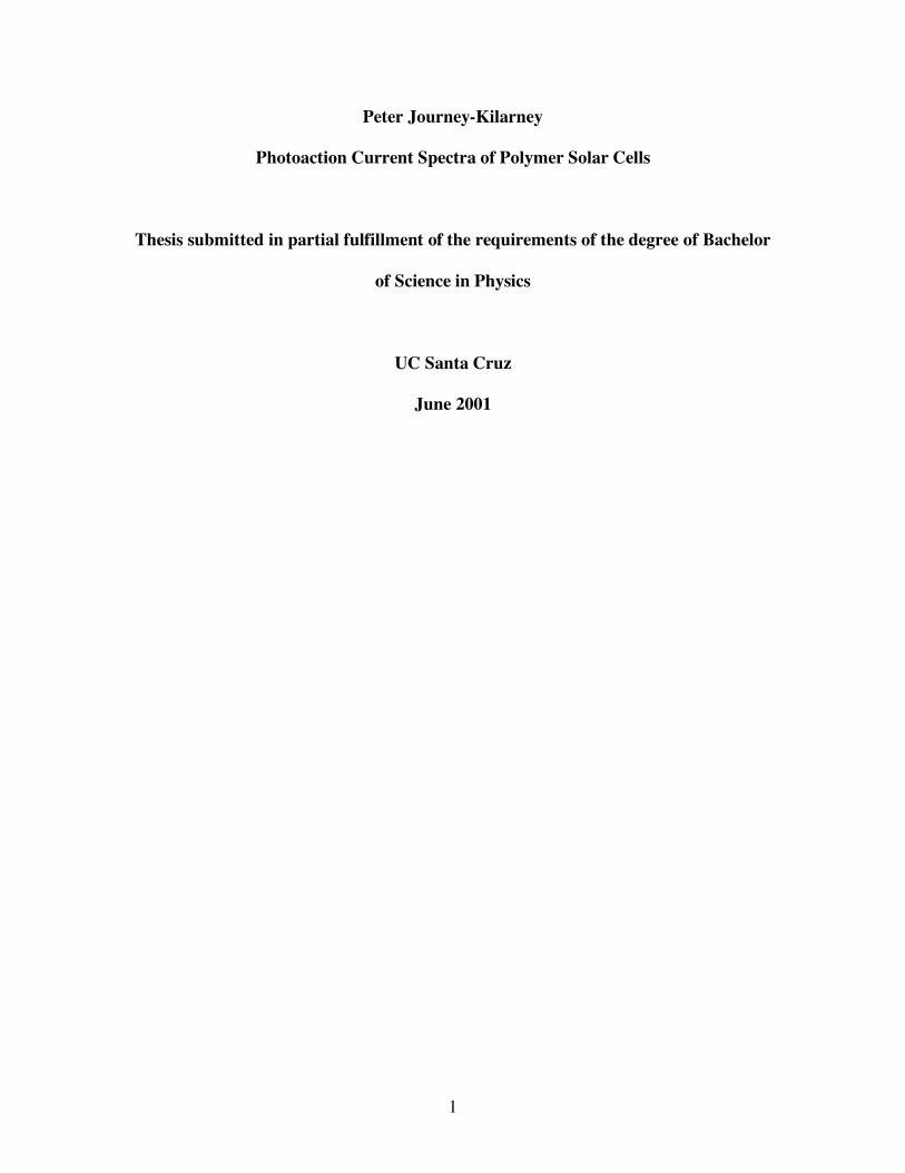
Blend Electron-Collector Configuration: Fig. 19 illustrates the EQE performances for
three blend devices, each with a different electron-collector. These devices represent to
best EQEs for their respective configurations. In sharp contrast with the M3EH devices,
it appears that for blends the TiOx / polymer interface is significantly more efficient at
exciton disassociation than the TiO2 / polymer interface. As a TiO2 / M3EH interface has
been seen to boost disassociation I assume that the drop in performance is connected to
the TiO2 / Cn –Ether interface in the blended devices. Unfortunately, time constraints
prevent any further investigation, but I would have liked to manufacture some straight Cn
– Ether devices with both TiOx and TiO2 to see what the effect of the different electron-
collectors would be on device EQE. My hypothesis is that using a TiO2 interface with Cn
– Ether inhibits exciton disassociation.

38
0
5
10
15
20
350 400 450 500 550 600 650
Fig.20: M3EH TiOx vs. Blend TiOx
M3EH (SCV 421.5)
Blend (SVC 402.5)
Wavelength ( nm )
EQE ( % )
M3EH versus Blend Performances: Fig. 20 gives a direct comparison between M3EH
and blend EQEs for the TiOx electron-collector. Fig. 20 clearly demonstrates that for the
TiOx / polymer configuration, blended M3EH and Cn – Ether outperforms straight
M3EH, with a peak EQE of 18.34% for the blend versus 6.56% for M3EH. This seems
to support the argument that the blended polymers phase separate and that the large
contact area created between theses polymer regions acts as an additional disassociation
interface. While the M3EH data for this graph agrees well with previously collected data,
the blend data, as noted before is actually lower than data from both NREL and UCSC.
This indicates that the performance bonuses of blended M3EH / Cn – Ether are even
greater than depicted in Fig. 20.
39
0
5
10
15
20
350 400 450 500 550 600 650
Fig.21: M3EH TiO2 vs. Blend TiO2
M3EH (MK 298.2)
Blend (MK 296.6)
Wavelength ( nm )
EQE ( % )
0
5
10
15
20
350 400 450 500 550 600 650
Fig. 22: M3EH TiOx/ TiO2 vs. Blend TiOx/ TiO2
Blend (MK 303.6)
M3EH (MK 268.5)
Wavelength ( nm )
EQE ( % )

40
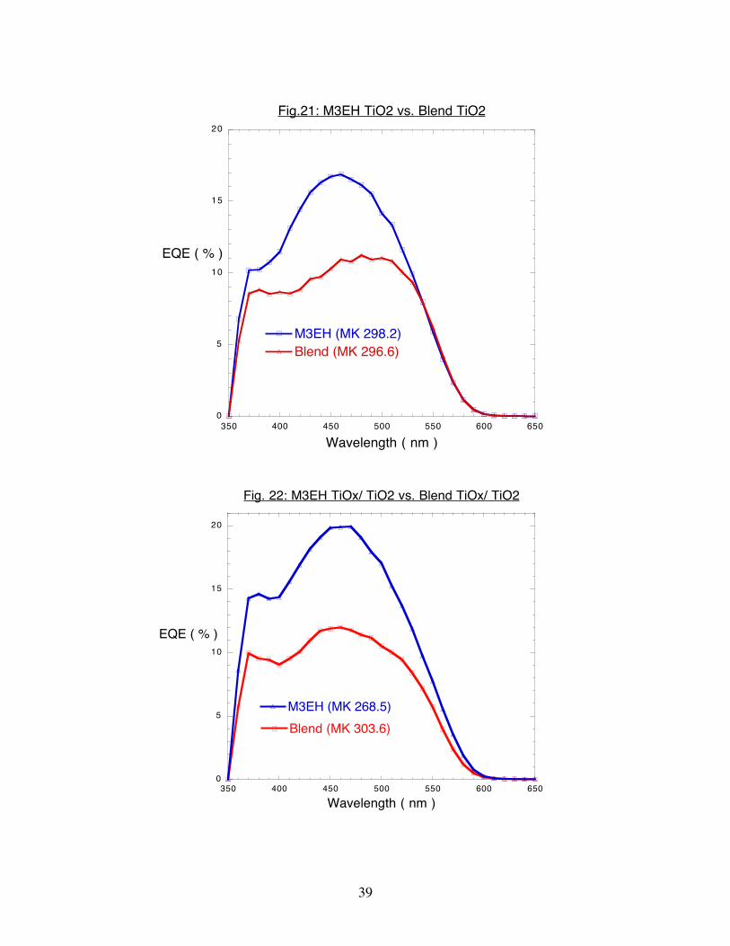
Fig. 21 and Fig. 22 compare blended devices to M3EH devices for the two TiO2 /
polymer interface configurations. These graphs illustrate that for both the TiO2 and TiOx
/ TiO2 interfaces the straight M3EH devices clearly outperform the blended polymer
devices. For the TiO2 interface M3EH gives a peak EQE of 16.78%, while blended
polymer gives only 11.23%. On the TiOx / TiO2 interface the difference is even more
pronounced with a peak EQE of 19.94% for M3EH versus 11.98% for the blend.
Considering that on the TiOx interface, blended polymer significantly boosted EQE
performance, these graph further indicate that the interaction between TiO2 and Cn –
Ether hampers exciton disassociation.
Conclusion:
In conclusion, my investigation of the six polymer solar cell configurations,
M3EH TiOx, M3EH TiO2, M3EH TiOx / TiO2, Blend TiOx, Blend TiO2 and Blend TiOx /
TiO2, has yielded some interesting and hopefully useful results. For polymer solar cells
based on straight M3EH – PPV, it has been shown that a TiOx / TiO2 / M3EH
disassociation interface delivers much higher external quantum efficiencies than a TiOx /
M3EH interface, with EQEs of 19.94% (TiOx / TiO2) versus 6.56% (TiOx). Although the
TiOx / TiO2 / M3EH configuration delivered the highest EQE for this experiment, I
believe that further investigation of the TiO2 only configuration may yield equally
impressive results. The results for the M3EH devices seem to confirm that the roughness
of the TiO2 layer does boost exciton disassociation. For the blended M3EH / Cn – Ether
devices the opposite behavior was observed. The Blend TiOx configuration achieved the
best EQE, 16.78%, while Blend TiO2 gave 11.23% and Blend TiOx / TiO2 gave 11.98%.

41
Considering that blended M3EH / Cn – Ether has been shown to greatly improve EQE on
a TiOx layer (16.78% versus 6.56% for straight M3EH) it seems that the interaction
between the Cn – Ether and TiO2 has a negative affect on exciton disassociation. I would
recommend investigating straight Cn – Ether on both TiOx and TiO2 layers to see how the
EQE is affected. If the TiO2 EQEs are significantly lower it would explain the drops in
blend EQEs that I have observed.
Once again I would like to emphasize that I had to collect most of my data during
a very short period, this led to small sample sizes for some of the device configurations,
which may have affected to quality of my data. Further investigation into the EQEs of
the six device configurations I examined as well as other cell architectures will enhance
the understanding of polymer solar cells and help to increase there efficiency. I hope that
the photoaction current spectra apparatus, which I assembled for this experiment will aid
Dr. Sue Carter in her continuing investigation of polymer solar cells. Maybe the
scientific breakthrough, which will allow solar power to take over as the world’s key
source of energy will take place here at UCSC, then I will have remote bragging rights to
making the world a better place.
Thank you:
This report would not be complete with out some very heart-felt thanks. Thank
you to Dr. Sue Cater for allowing me to work in your lab, for all your assistance with this
project and my grad school applications and for paying me so that I could feed myself
you have been a great help and an inspiration to pursue a career in research. Thank you
to Dr. Melissa Kreger for teaching me so much, putting up with my endless questions and

42
for donating your solar cells, I never could have figured out my way around the lab with
out your help. Thanks to Stephanie Chasteen, who also donated solar cells, without
which my report would have been impossible to complete. Thanks for working late
Steph; I hope my data helps you finish your thesis. Thank you to Yuko Nakazawa for
helping me with the LabView programming, you saved me weeks of work, good luck
finishing up with school. Thank you all the folks in Sue’s lab for your help and support,
thanks Tosan, Janelle, and Eric. Finally thank you so much to my parents, Robert and
Carol and to my beloved brother and sister, Geoffrey and Stephanie. I would have never
even tried to come this far with out your love and devotion.
i Improved Performance Polymer – Inorganic Composite Photovoltaics. Breeze, Allison J. USCS, 2000 ii Illustration donated generously by Stephanie V. Chasteen iii TiOx Layer in Plastic Solar Cells. Omabegha, Tosan UCSC 2002 iv TiOx Layer in Plastic Solar Cells. Omabegha, Tosan UCSC 2002