phy 4240 lec (7)
DESCRIPTION
Introduction to semiconductor physicsTRANSCRIPT
An Introduction to
Semiconductor
Materials
Lecture (7)
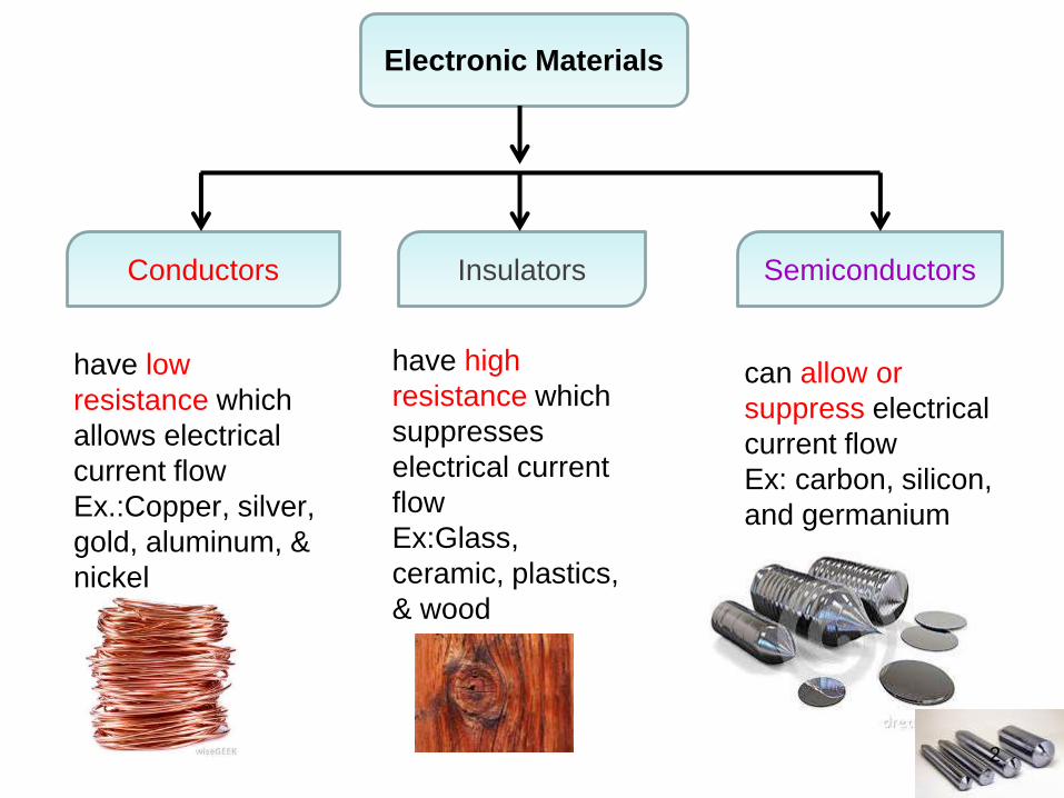
Conductors Insulators Semiconductors
Electronic Materials
have low
resistance which
allows electrical
current flow
Ex.:Copper, silver,
gold, aluminum, &
nickel
have high
resistance which
suppresses
electrical current
flow
Ex:Glass,
ceramic, plastics,
& wood
can allow or
suppress electrical
current flow
Ex: carbon, silicon,
and germanium
2
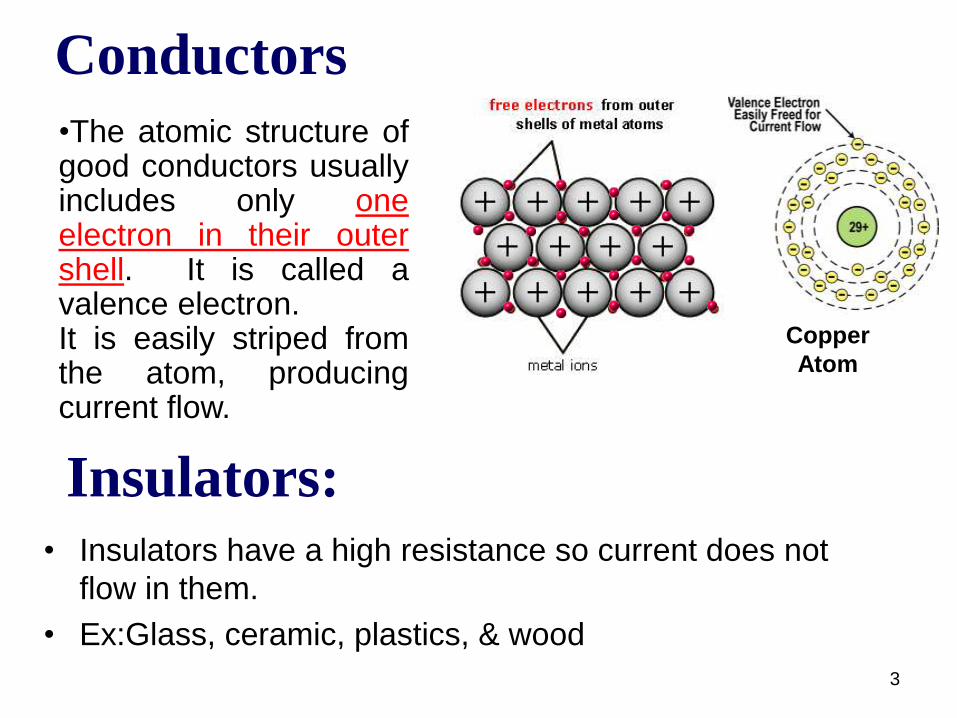
Conductors
Copper
Atom
Insulators:• Insulators have a high resistance so current does not
flow in them.
• Ex:Glass, ceramic, plastics, & wood
3
•The atomic structure ofgood conductors usuallyincludes only oneelectron in their outershell. It is called avalence electron.It is easily striped fromthe atom, producingcurrent flow.
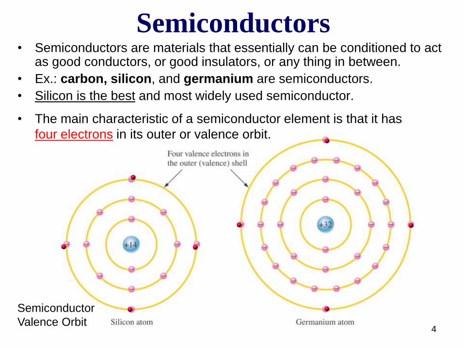
• Semiconductors are materials that essentially can be conditioned to actas good conductors, or good insulators, or any thing in between.
• Ex.: carbon, silicon, and germanium are semiconductors.
• Silicon is the best and most widely used semiconductor.
Semiconductors
• The main characteristic of a semiconductor element is that it has
four electrons in its outer or valence orbit.
Semiconductor
Valence Orbit4
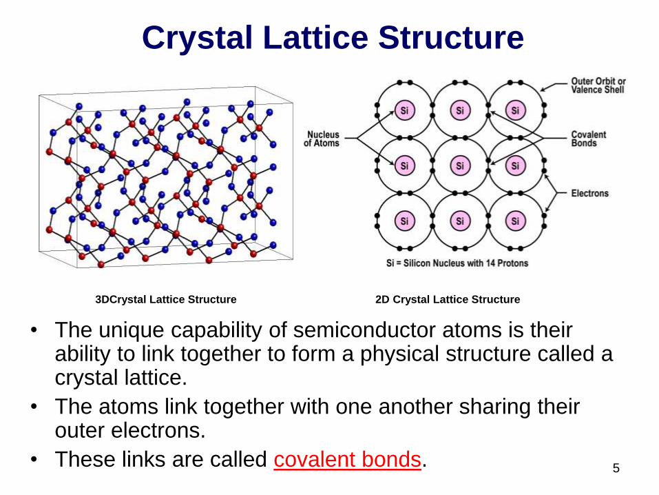
Crystal Lattice Structure
• The unique capability of semiconductor atoms is their ability to link together to form a physical structure called a crystal lattice.
• The atoms link together with one another sharing their outer electrons.
• These links are called covalent bonds.
3DCrystal Lattice Structure 2D Crystal Lattice Structure
5
6
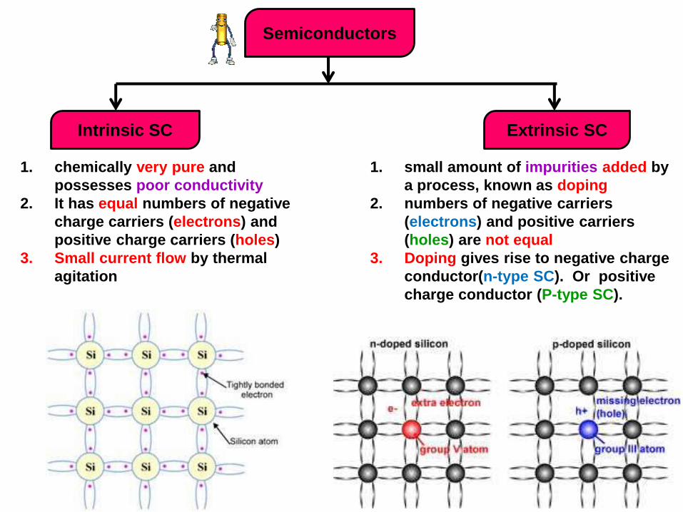
Semiconductors
Intrinsic SC Extrinsic SC
1. chemically very pure and
possesses poor conductivity
2. It has equal numbers of negative
charge carriers (electrons) and
positive charge carriers (holes)
3. Small current flow by thermal
agitation
1. small amount of impurities added by
a process, known as doping
2. numbers of negative carriers
(electrons) and positive carriers
(holes) are not equal
3. Doping gives rise to negative charge
conductor(n-type SC). Or positive
charge conductor (P-type SC).
7
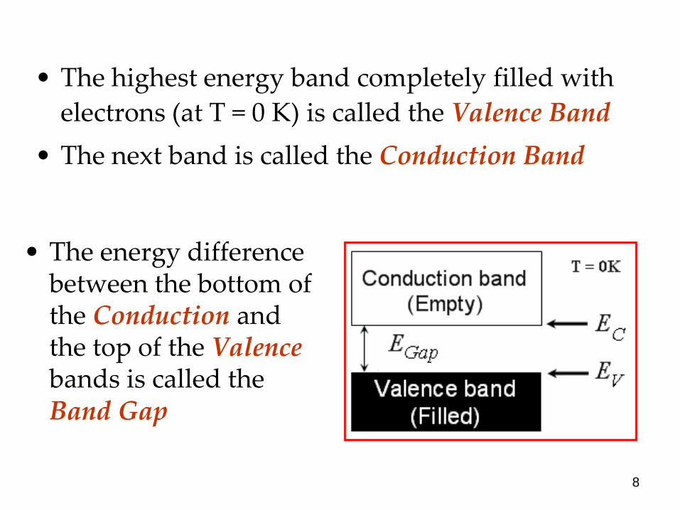
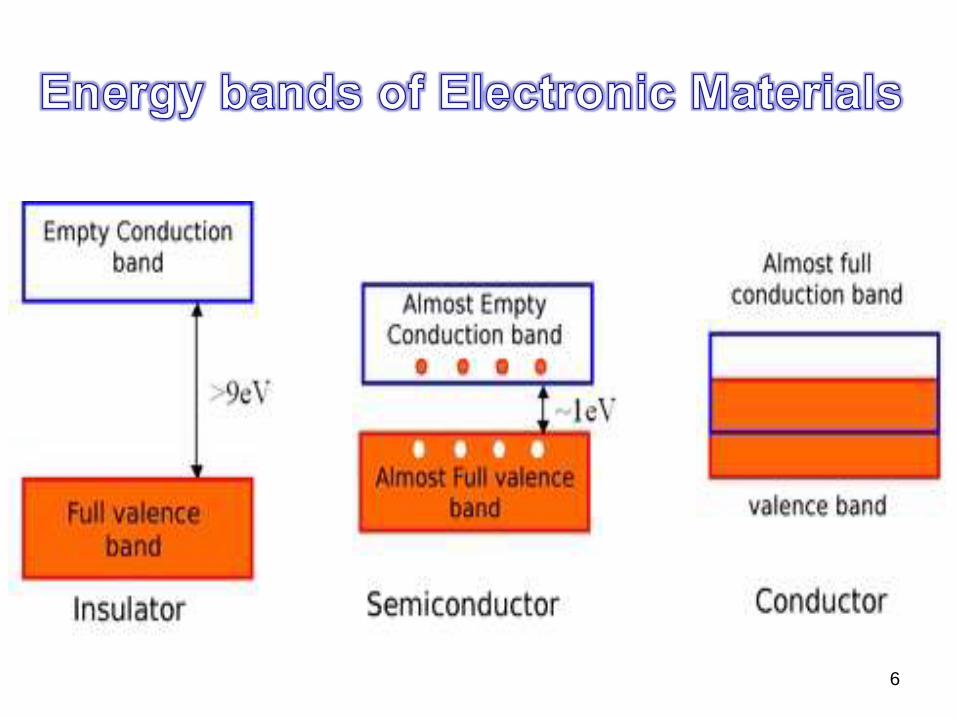
• The highest energy band completely filled with
electrons (at T = 0 K) is called the Valence Band
• The next band is called the Conduction Band
• The energy difference between the bottom of the Conduction and the top of the Valencebands is called the Band Gap
8
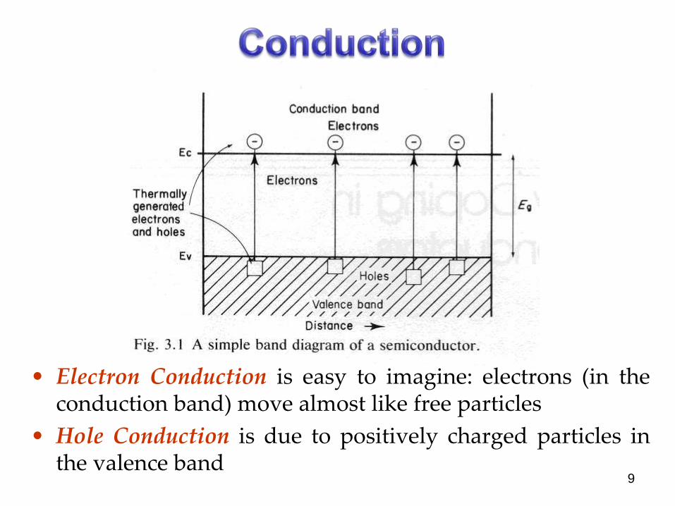
• Electron Conduction is easy to imagine: electrons (in theconduction band) move almost like free particles
• Hole Conduction is due to positively charged particles inthe valence band
9
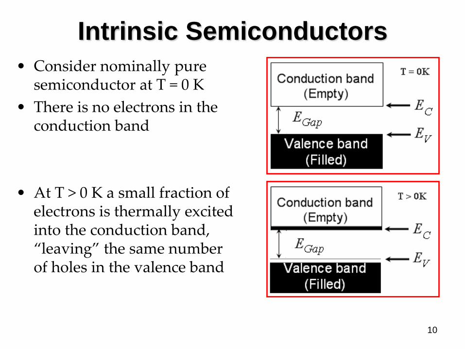
Intrinsic Semiconductors
• Consider nominally pure semiconductor at T = 0 K
• There is no electrons in the conduction band
• At T > 0 K a small fraction of electrons is thermally excited into the conduction band, “leaving” the same number of holes in the valence band
10
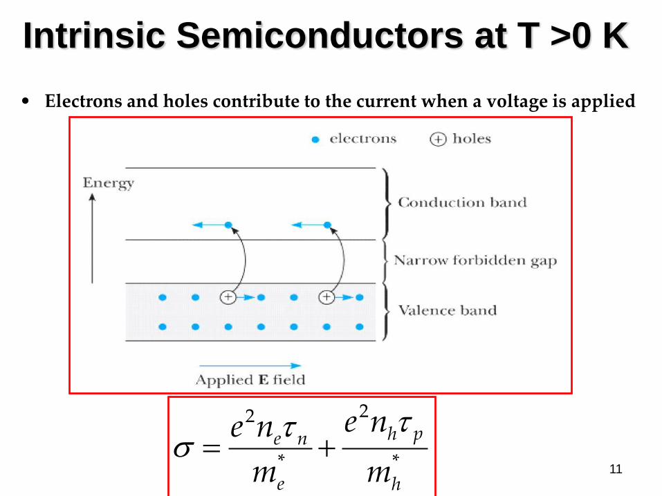
Intrinsic Semiconductors at T >0 K
• Electrons and holes contribute to the current when a voltage is applied
*
2
*
2
h
ph
e
ne
m
ne
m
ne
11
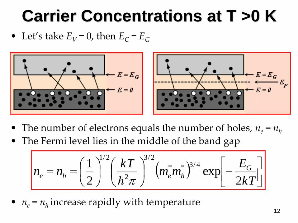
Carrier Concentrations at T >0 K• Let’s take EV = 0, then EC = EG
• The number of electrons equals the number of holes, ne = nh
• The Fermi level lies in the middle of the band gap
• ne = nh increase rapidly with temperature
kT
Emm
kTnn G
hehe2
exp2
1 4/3**
2/3
2
2/1
12
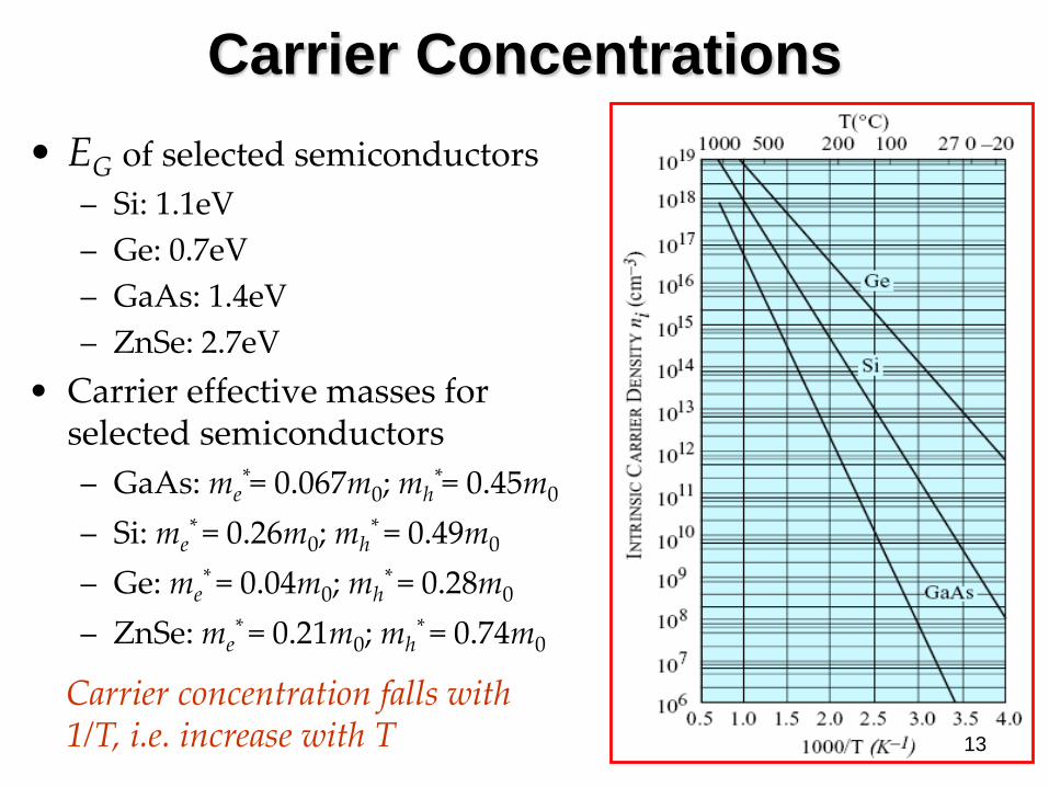
Carrier Concentrations
• EG of selected semiconductors
– Si: 1.1eV
– Ge: 0.7eV
– GaAs: 1.4eV
– ZnSe: 2.7eV
• Carrier effective masses for selected semiconductors
– GaAs: me*= 0.067m0; mh
*= 0.45m0
– Si: me* = 0.26m0; mh
* = 0.49m0
– Ge: me* = 0.04m0; mh
* = 0.28m0
– ZnSe: me* = 0.21m0; mh
* = 0.74m0
Carrier concentration falls with 1/T, i.e. increase with T 13
• Semiconductors can be easily doped
• Doping is the incorporation of [substitutional] impurities into a semiconductor according to our requirements
• In other words, impurities are introduced ina controlled manner
• Impurities change the conductivity of thematerial so that it can be fabricated into adevice
14
Extrinsic Semiconductors
• Electrical Properties of Semiconductors can be altered drastically by adding minute amounts of suitable impurities to the pure crystals
• Impurities: Atoms of the elements different from those forming solid
– Interstitial: “foreign” atoms “squeezed” between regular sites crystal sites
– Substitutional: “foreign” atoms occupying the sites of host atoms
15
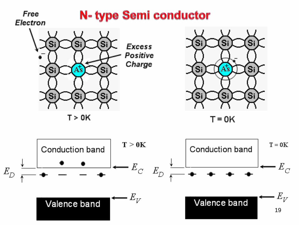
Donors
• We use Silicon (Si) as an example
– Substitute one Si (Group IV) atom with a Group V atom (e.g. As or P)
– Si atoms have four valence electrons that participate in covalent bonding
– When a Group V atom replaces a Si atom, it will use four of its electrons to form the covalent bonding
– What happens with the remaining electron?
16
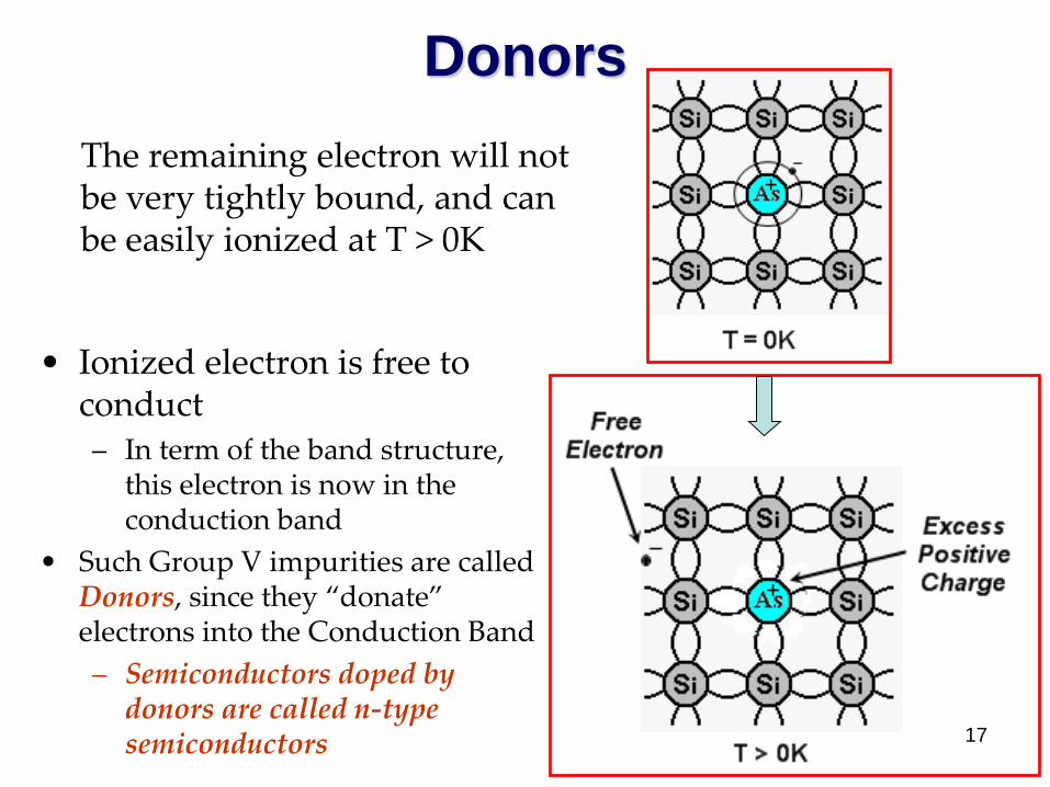
Donors
• Ionized electron is free to conduct– In term of the band structure,
this electron is now in the conduction band
• Such Group V impurities are called Donors, since they “donate” electrons into the Conduction Band
– Semiconductors doped by donors are called n-type semiconductors 17
The remaining electron will not be very tightly bound, and can be easily ionized at T > 0K
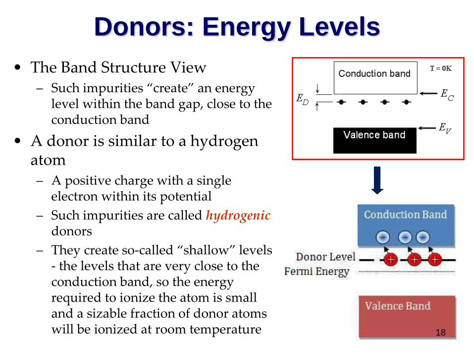
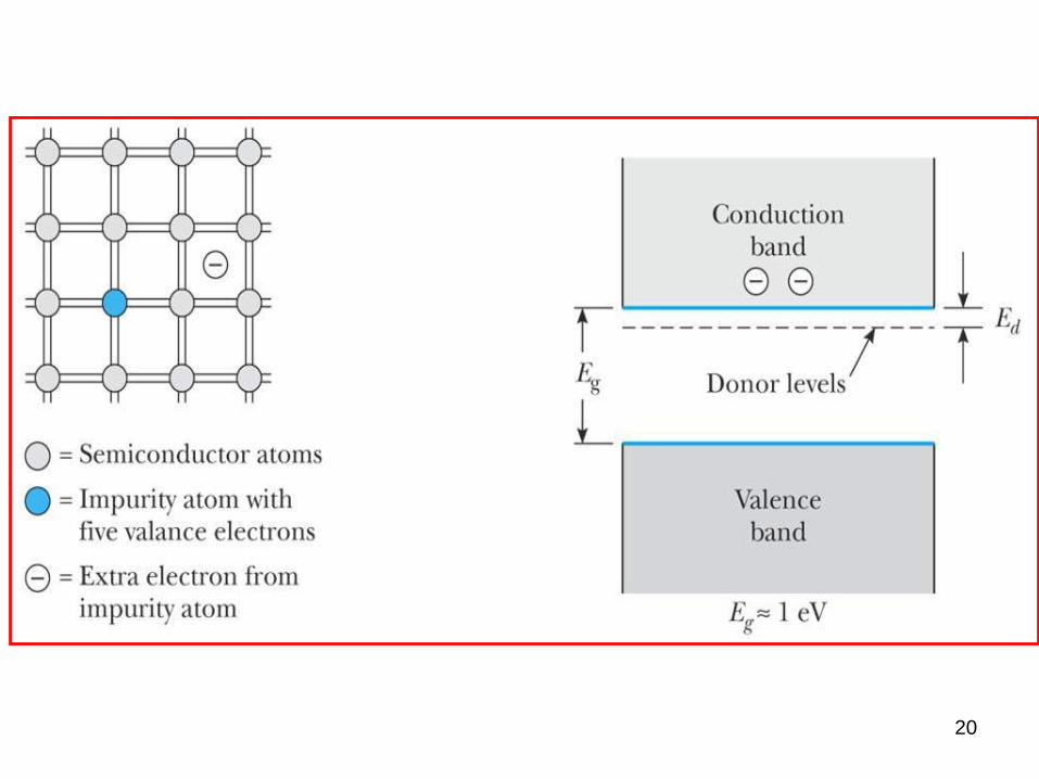
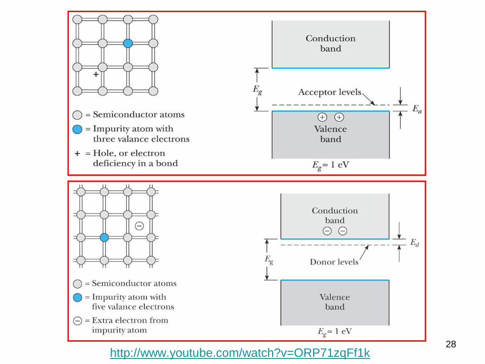
Donors: Energy Levels
• The Band Structure View– Such impurities “create” an energy
level within the band gap, close to the conduction band
• A donor is similar to a hydrogen atom– A positive charge with a single
electron within its potential
– Such impurities are called hydrogenicdonors
– They create so-called “shallow” levels - the levels that are very close to the conduction band, so the energy required to ionize the atom is small and a sizable fraction of donor atoms will be ionized at room temperature 18
19
20
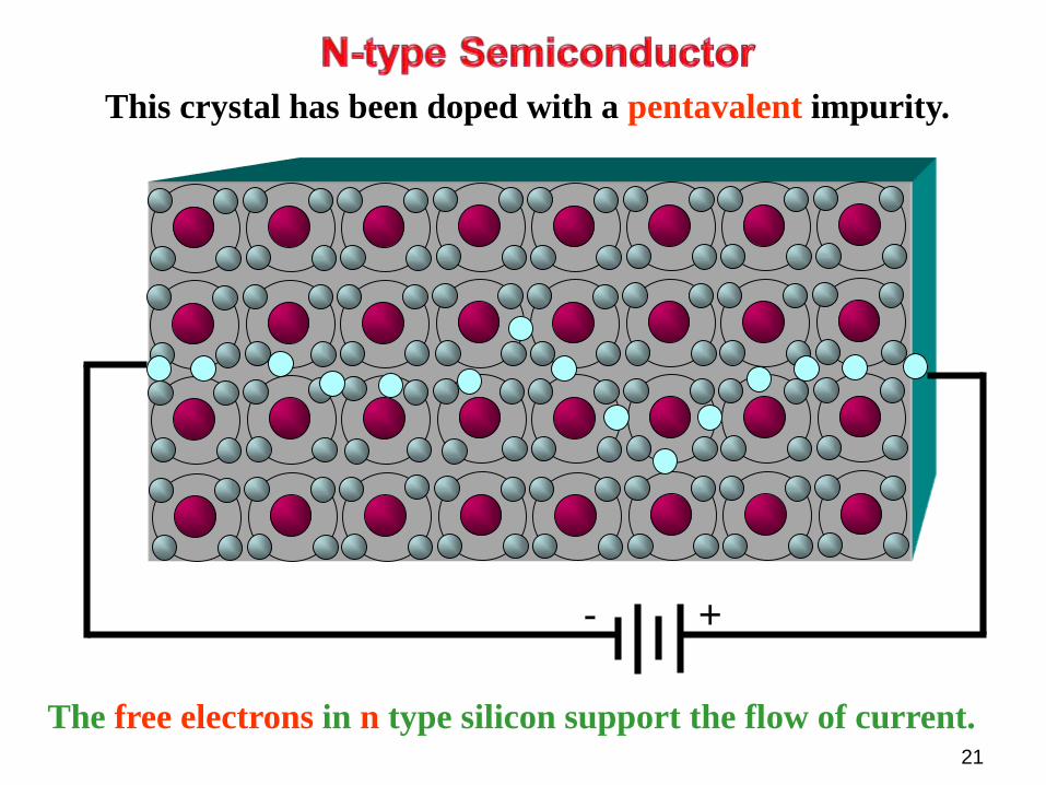
The free electrons in n type silicon support the flow of current.
This crystal has been doped with a pentavalent impurity.
- +
21
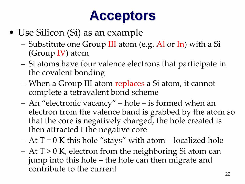
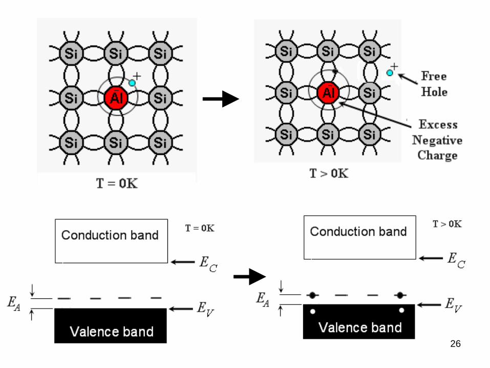
Acceptors• Use Silicon (Si) as an example
– Substitute one Group III atom (e.g. Al or In) with a Si (Group IV) atom
– Si atoms have four valence electrons that participate in the covalent bonding
– When a Group III atom replaces a Si atom, it cannot complete a tetravalent bond scheme
– An “electronic vacancy” – hole – is formed when an electron from the valence band is grabbed by the atom so that the core is negatively charged, the hole created is then attracted t the negative core
– At T = 0 K this hole “stays” with atom – localized hole
– At T > 0 K, electron from the neighboring Si atom can jump into this hole – the hole can then migrate and contribute to the current
22
Acceptors
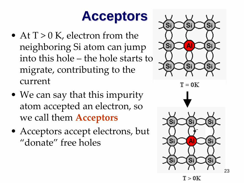
• At T > 0 K, electron from the neighboring Si atom can jump into this hole – the hole starts to migrate, contributing to the current
• We can say that this impurity atom accepted an electron, so we call them Acceptors
• Acceptors accept electrons, but “donate” free holes
23
Acceptors
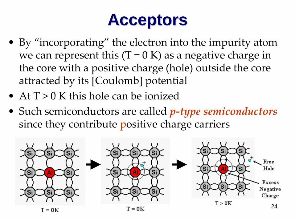
• By “incorporating” the electron into the impurity atom we can represent this (T = 0 K) as a negative charge in the core with a positive charge (hole) outside the core attracted by its [Coulomb] potential
• At T > 0 K this hole can be ionized
• Such semiconductors are called p-type semiconductors since they contribute positive charge carriers
24
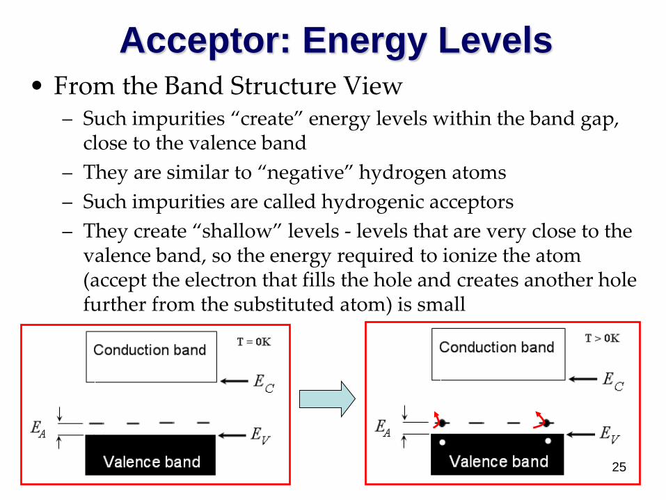
Acceptor: Energy Levels• From the Band Structure View
– Such impurities “create” energy levels within the band gap, close to the valence band
– They are similar to “negative” hydrogen atoms
– Such impurities are called hydrogenic acceptors
– They create “shallow” levels - levels that are very close to the valence band, so the energy required to ionize the atom (accept the electron that fills the hole and creates another hole further from the substituted atom) is small
25
26
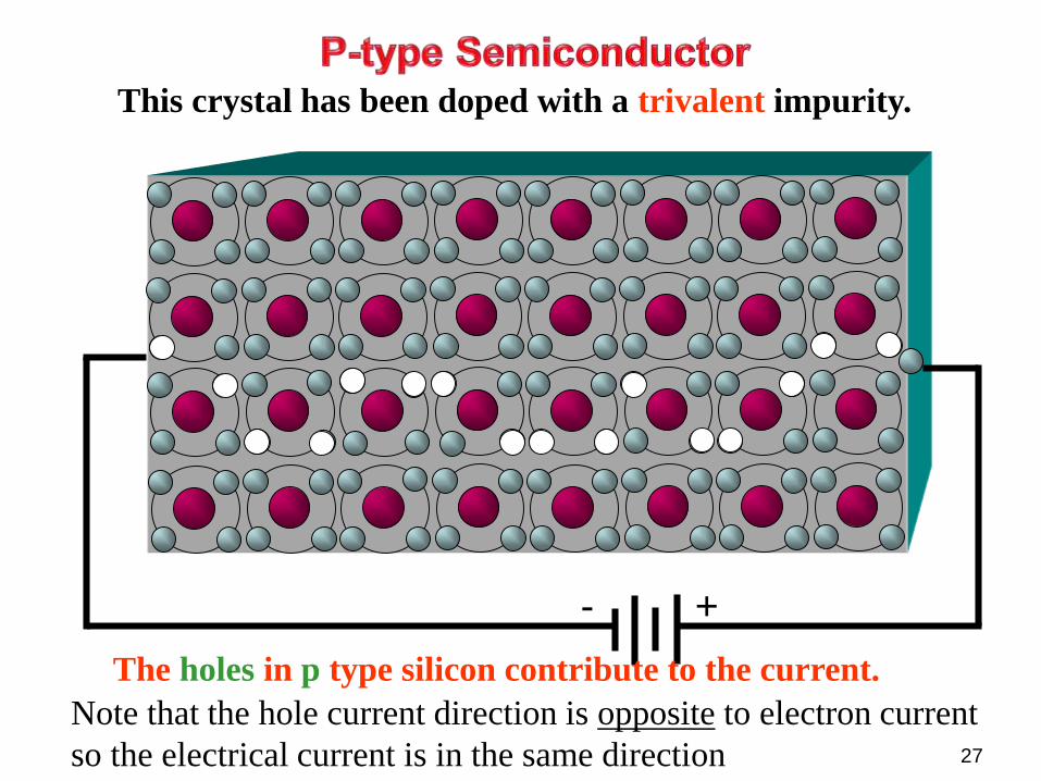
This crystal has been doped with a trivalent impurity.
The holes in p type silicon contribute to the current.
Note that the hole current direction is opposite to electron current
so the electrical current is in the same direction
- +
27
http://www.youtube.com/watch?v=ORP71zqFf1k28
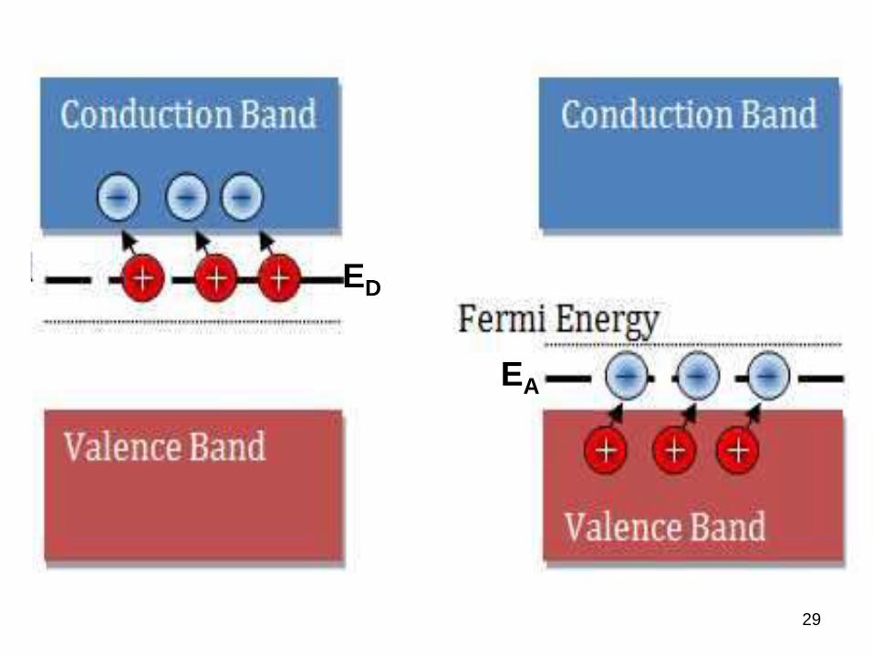
29
ED
EA
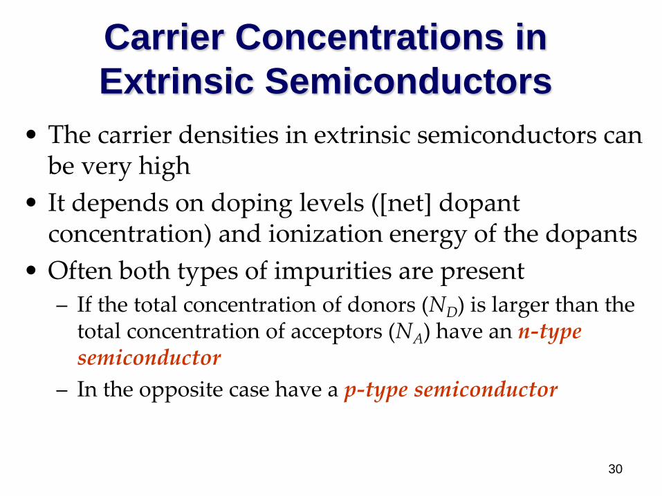
Carrier Concentrations in
Extrinsic Semiconductors
• The carrier densities in extrinsic semiconductors can be very high
• It depends on doping levels ([net] dopant concentration) and ionization energy of the dopants
• Often both types of impurities are present
– If the total concentration of donors (ND) is larger than the total concentration of acceptors (NA) have an n-type semiconductor
– In the opposite case have a p-type semiconductor
30
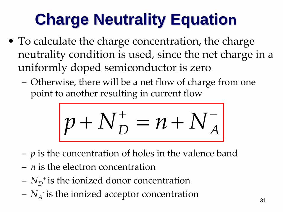
Charge Neutrality Equation
• To calculate the charge concentration, the charge neutrality condition is used, since the net charge in a uniformly doped semiconductor is zero
– Otherwise, there will be a net flow of charge from one point to another resulting in current flow
– p is the concentration of holes in the valence band
– n is the electron concentration
– ND+ is the ionized donor concentration
– NA- is the ionized acceptor concentration
AD NnNp
31
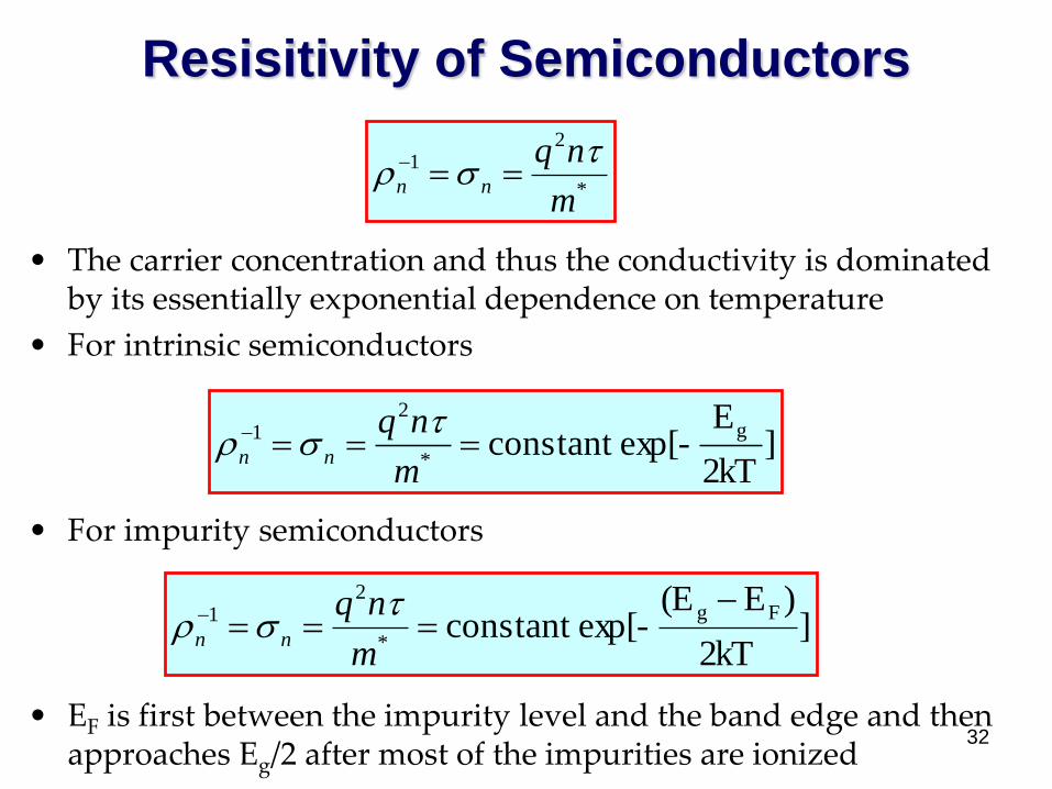
Resisitivity of Semiconductors
• The carrier concentration and thus the conductivity is dominated by its essentially exponential dependence on temperature
• For intrinsic semiconductors
• For impurity semiconductors
• EF is first between the impurity level and the band edge and then approaches Eg/2 after most of the impurities are ionized
*
21
m
nqnn
]2kT
Eexp[-constant
g
*
21
m
nqnn
]2kT
)E(Eexp[-constant
Fg
*
21
m
nqnn
32
Semiconductors in Summary
• The most widely used material is silicon
• Pure crystals are intrinsic semiconductors
• Doped crystals are extrinsic semiconductors
• Crystals are doped to be n type or p type
• n type semiconductors have few minority
carriers (holes).
• p type semiconductors have few minority
carriers (electrons).
33
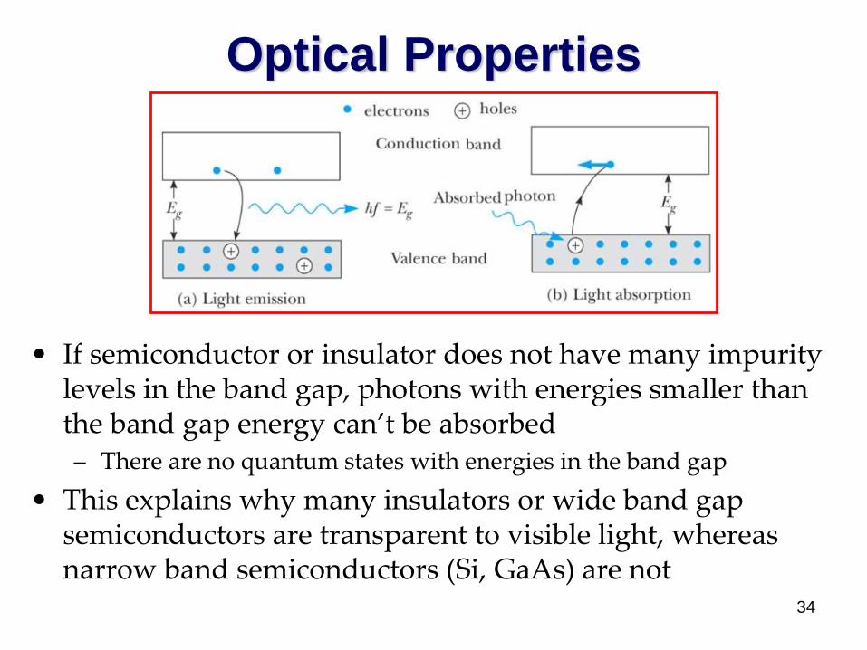
Optical Properties
• If semiconductor or insulator does not have many impurity levels in the band gap, photons with energies smaller than the band gap energy can’t be absorbed– There are no quantum states with energies in the band gap
• This explains why many insulators or wide band gap semiconductors are transparent to visible light, whereas narrow band semiconductors (Si, GaAs) are not
34
Optical Properties
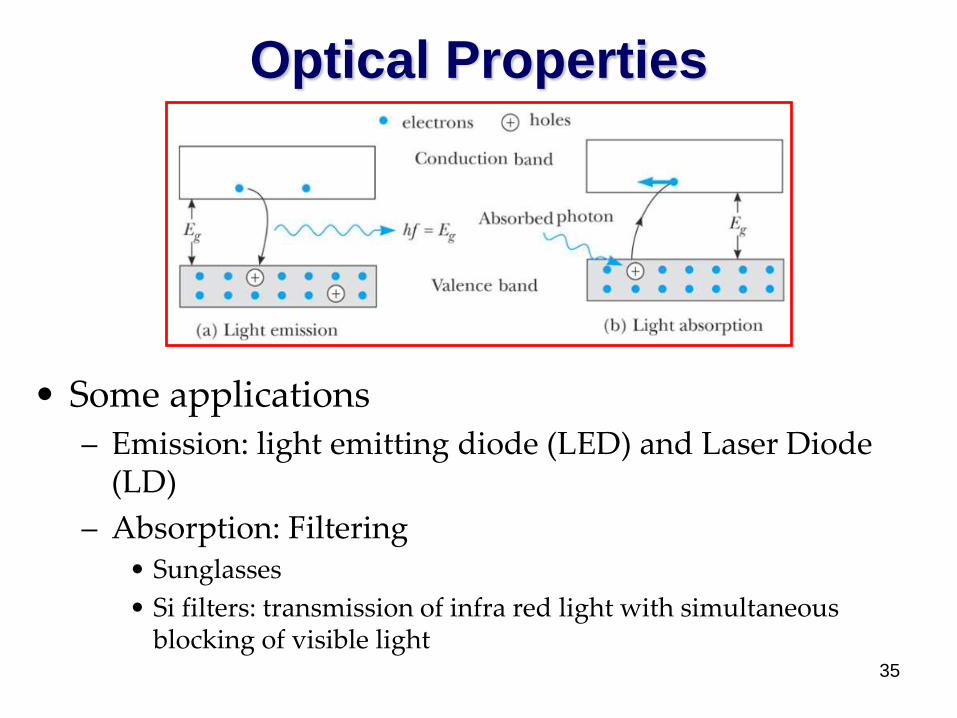
• Some applications
– Emission: light emitting diode (LED) and Laser Diode (LD)
– Absorption: Filtering• Sunglasses
• Si filters: transmission of infra red light with simultaneous blocking of visible light
35
Optical Properties
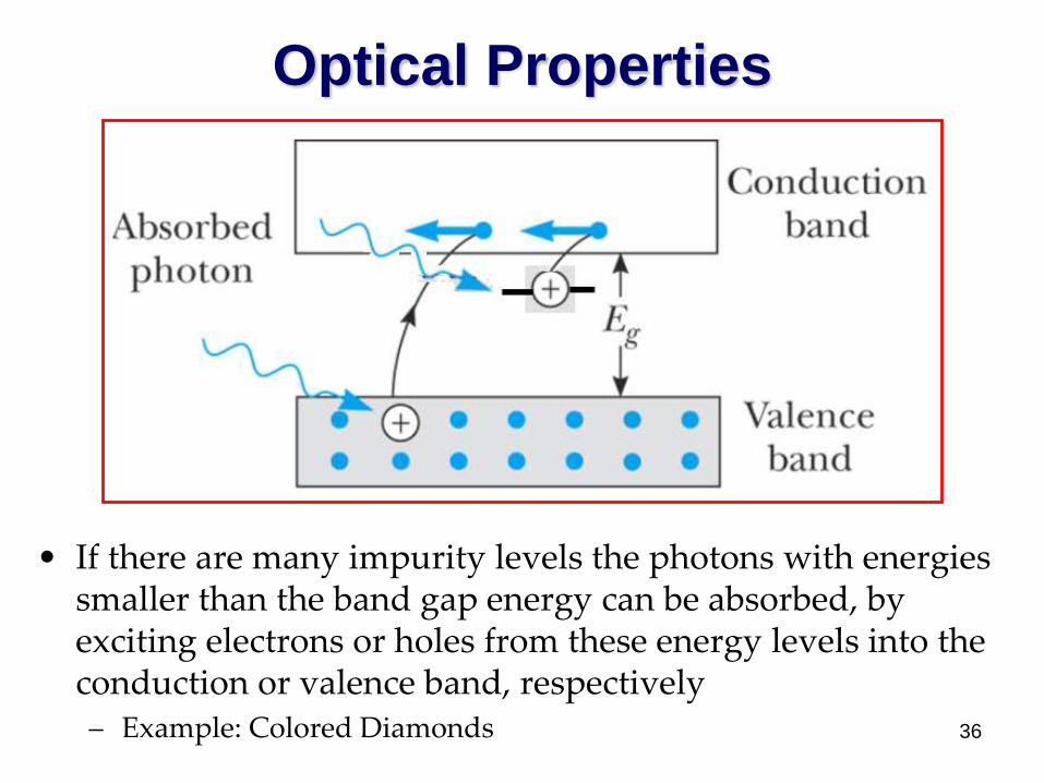
• If there are many impurity levels the photons with energies smaller than the band gap energy can be absorbed, by exciting electrons or holes from these energy levels into the conduction or valence band, respectively– Example: Colored Diamonds 36
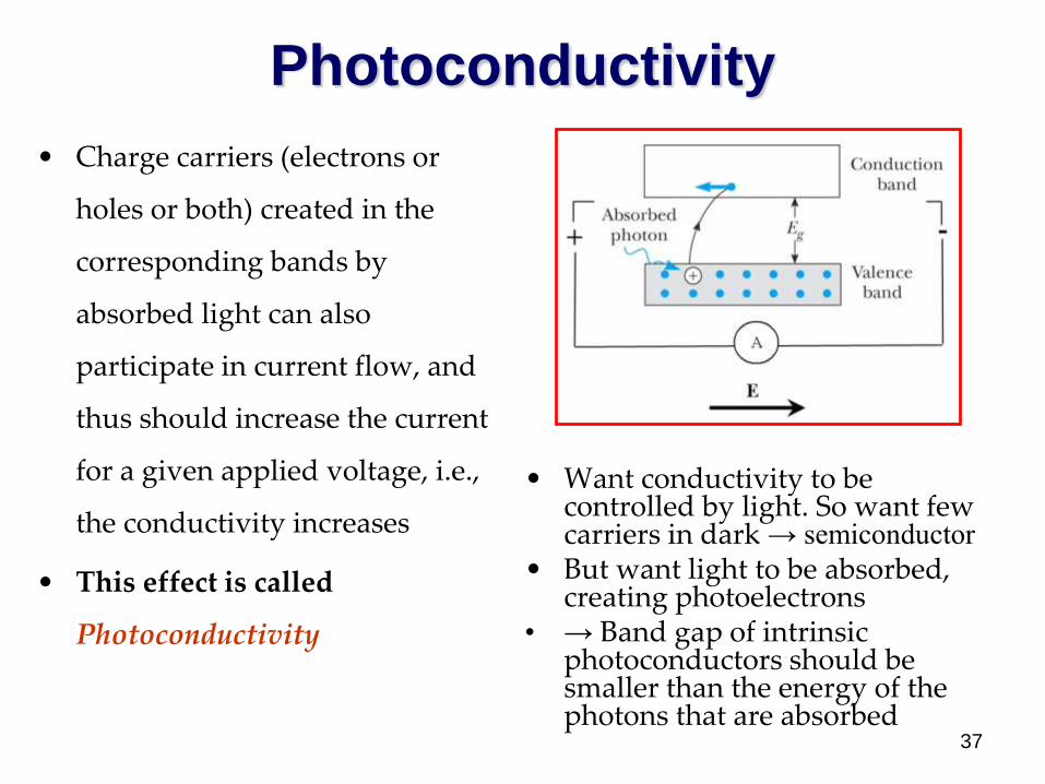
Photoconductivity
• Charge carriers (electrons or
holes or both) created in the
corresponding bands by
absorbed light can also
participate in current flow, and
thus should increase the current
for a given applied voltage, i.e.,
the conductivity increases
• This effect is called
Photoconductivity
• Want conductivity to be controlled by light. So want few carriers in dark → semiconductor
• But want light to be absorbed, creating photoelectrons
• → Band gap of intrinsic photoconductors should be smaller than the energy of the photons that are absorbed
37
Photoconductivity
• Important Applications (Garcia 26.6)
– Night vision systems imaging IR radiation
– Solar cells
– Radiation detectors
– Photoelectric cells (e.g., used for automatic doors)
– Xerography
– CCD (“Digital Cameras”)
38