physical structure of cmos integrated circuitsee434/handouts/02-physical_structure.pdf · physical...
TRANSCRIPT

Physical Structure of CMOS Integrated Circuits
Dae Hyun Kim
EECS Washington State University

References
• John P. Uyemura, “Introduction to VLSI Circuits and Systems,” 2002. – Chapter 3
• Neil H. Weste and David M. Harris, “CMOS VLSI Design: A Circuits and Systems Perspective,” 2011. – Chapter 1

Goal
• Understand the physical structure of CMOS integrated circuits (ICs)

Logical vs. Physical
• Logical structure
• Physical structure
𝑏𝑏 𝑐𝑐
𝑎𝑎
𝑓𝑓
Source: http://www.vlsi-expert.com/2014/11/cmos-layout-design.html

Integrated Circuit Layers
• Semiconductor – Transistors (active elements)
• Conductor
– Metal (interconnect) • Wire • Via
• Insulator
– Separators

Integrated Circuit Layers
• Silicon substrate, insulator, and two wires (3D view)
• Side view
• Top view
Substrate
Insulator
Metal 1 layer
Substrate

Integrated Circuit Layers
• Two metal layers separated by insulator (side view)
• Top view
Substrate
Metal 1 layer
Metal 2 layer
Insulator
Insulator Via 12 (connecting M1 and M2)
Connected Not connected

Integrated Circuit Layers

Integrated Circuit Layers
• Signal transfer speed is affected by the interconnect resistance and capacitance. – Resistance ↑ => Signal delay ↑ – Capacitance ↑ => Signal delay ↑

Integrated Circuit Layers
• Resistance – 𝑅𝑅 = 𝜌𝜌 𝑙𝑙
𝐴𝐴= 𝜌𝜌
𝑡𝑡∙ 𝑙𝑙𝑤𝑤
= 𝑅𝑅𝑠𝑠 ∙𝑙𝑙𝑤𝑤
• 𝑅𝑅𝑠𝑠: sheet resistance (constant)
• 𝜌𝜌: resistivity (= 1𝜎𝜎, 𝜎𝜎: conductivity)
– Material property (constant) – Unit: Ω ∙ 𝑚𝑚
• 𝑡𝑡: thickess (constant) • 𝑤𝑤: width (variable) • 𝑙𝑙: length (variable)
• Example
– 𝜌𝜌: 17.1𝑛𝑛Ω ∙ 𝑚𝑚, 𝑡𝑡: 0.13𝜇𝜇𝑚𝑚,𝑤𝑤: 65𝑛𝑛𝑚𝑚, 𝑙𝑙: 1000𝜇𝜇𝑚𝑚
• 𝑅𝑅 = 17.1 ∙ 10−9Ω ∙ 𝑚𝑚 ∙ 1000∙10−6𝑚𝑚0.13∙10−6𝑚𝑚 ∙ 65∙10−9𝑚𝑚
= 2023Ω
𝑤𝑤
Direction of current flows
𝑙𝑙 𝑡𝑡
Cross-sectional area 𝐴𝐴 = 𝑡𝑡 ∙ 𝑤𝑤

Integrated Circuit Layers
• Capacitance – 𝐶𝐶 = 𝜀𝜀 𝑡𝑡∙𝑙𝑙
𝑠𝑠
• 𝜀𝜀: permittivity – Material property (constant) – Unit: F/m
• 𝑠𝑠: distance between two conductors
• Example
– 𝜀𝜀: 1.8 ∙ 10−11𝐹𝐹/𝑚𝑚, 𝑡𝑡: 0.13𝜇𝜇𝑚𝑚, 𝑠𝑠: 65𝑛𝑛𝑚𝑚, 𝑙𝑙: 1000𝜇𝜇𝑚𝑚
• 𝐶𝐶 = 1.8 ∙ 10−11𝐹𝐹/𝑚𝑚 ∙ 0.13∙10−6𝑚𝑚 ∙ 1000∙10−6𝑚𝑚65∙10−9𝑚𝑚
= 3.6 ∙ 10−14𝐹𝐹 = 36𝑓𝑓𝐹𝐹
𝑠𝑠
Direction of current flows
𝑙𝑙 𝑡𝑡

MOSFETs – Physical Shape
• What a MOSFET looks like at the physical level – 𝐿𝐿: Channel length – 𝑊𝑊: Channel width
– 𝑊𝑊𝐿𝐿
: Aspect ratio
Substrate (silicon wafer)
Drain (D)
Source (S)
Silicon dioxide =
Gate oxide (insulator)
𝑳𝑳
Gate (G)
𝑾𝑾
S D
G
𝑳𝑳 G S D 𝑾𝑾
Top view Side view
Current flows

MOSFETs – Physical Shape
• Inverter
Source: Neil H. Weste and David M. Harris, “CMOS VLSI Design: A Circuits and Systems Perspective,” 2011

MOSFETs – Device Physics
• Atomic density of a silicon crystal – 𝑁𝑁𝑆𝑆𝑆𝑆 ≈ 5 × 10²²
• Intrinsic carrier density
– # free electrons (due to thermal excitations) – 𝑛𝑛𝑆𝑆 ≈ 1.45 × 10¹⁰/𝑐𝑐𝑚𝑚3 (at room temperature)
• Mass action law when no current flows in pure silicon
– 𝑛𝑛 = 𝑝𝑝 = 𝑛𝑛𝑆𝑆 – 𝑛𝑛𝑝𝑝 = 𝑛𝑛𝑆𝑆2
• 𝑛𝑛: # free electrons • 𝑝𝑝: # free holes

MOSFETs – Device Physics
• Doping – Add impurity atoms (dopants) to enhance # electrons or # holes. – n-type material: if more electrons are added (donors).
• 𝑁𝑁𝑑𝑑: # donors (1016~1019/𝑐𝑐𝑚𝑚3) • # free electrons (majority carriers): 𝑛𝑛𝑛𝑛 ≈ 𝑁𝑁𝑑𝑑/𝑐𝑐𝑚𝑚3
• # holes (minority carriers): 𝑝𝑝𝑛𝑛 ≈𝑛𝑛𝑖𝑖2
𝑁𝑁𝑑𝑑/𝑐𝑐𝑚𝑚3
• 𝑛𝑛𝑛𝑛 ≫ 𝑝𝑝𝑛𝑛 – p-type material: if more holes are added (acceptors).
• 𝑁𝑁𝑎𝑎: # acceptors (1014~1019/𝑐𝑐𝑚𝑚3) • # holes (majority carriers): 𝑝𝑝𝑝𝑝 ≈ 𝑁𝑁𝑎𝑎/𝑐𝑐𝑚𝑚3
• # free electrons (minority carriers): 𝑛𝑛𝑝𝑝 ≈𝑛𝑛𝑖𝑖2
𝑁𝑁𝑎𝑎/𝑐𝑐𝑚𝑚3
• 𝑝𝑝𝑝𝑝 ≫ 𝑛𝑛𝑝𝑝
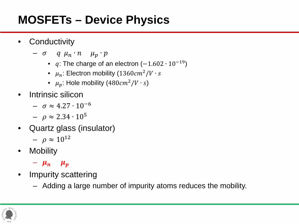
MOSFETs – Device Physics
• Conductivity – 𝜎𝜎 = 𝑞𝑞(𝜇𝜇𝑛𝑛 ∙ 𝑛𝑛 + 𝜇𝜇𝑝𝑝 ∙ 𝑝𝑝)
• 𝑞𝑞: The charge of an electron (−1.602 ∙ 10−19) • 𝜇𝜇𝑛𝑛: Electron mobility (1360𝑐𝑐𝑚𝑚2/𝑉𝑉 ∙ 𝑠𝑠) • 𝜇𝜇𝑝𝑝: Hole mobility (480𝑐𝑐𝑚𝑚2/𝑉𝑉 ∙ 𝑠𝑠)
• Intrinsic silicon – 𝜎𝜎 ≈ 4.27 ∙ 10−6 – 𝜌𝜌 ≈ 2.34 ∙ 105
• Quartz glass (insulator) – 𝜌𝜌 ≈ 1012
• Mobility – 𝝁𝝁𝒏𝒏 > 𝝁𝝁𝒑𝒑
• Impurity scattering – Adding a large number of impurity atoms reduces the mobility.

PN Junction
p
n
p
n
p
n
Forward current
𝐼𝐼 > 0
𝐼𝐼 > 0 𝐼𝐼 = 0
𝐼𝐼 = 0
Reverse blocking pn junction

MOSFETs
n+ n+
G
nFET
n+: heavily doped with donors
p
Contact (metal)
p+ p+
G
pFET
p+: heavily doped with acceptors
p
Contact (metal)
n-well
* Contacts are used to connect source/drain/gate to metal 1.

MOSFETs – Device Physics
• 𝑡𝑡𝑜𝑜𝑜𝑜: oxide thickness – Typically a few nm
• Gate material – Polysilicon (called poly) – Metal
• Oxide capacitance (Gate(M) – Insulator(O) – Semiconductor(S)) – 𝐶𝐶𝐺𝐺 = 𝑐𝑐𝑜𝑜𝑜𝑜 ∙ 𝐴𝐴𝐺𝐺
• 𝑐𝑐𝑜𝑜𝑜𝑜 = 𝜀𝜀𝑜𝑜𝑜𝑜𝑡𝑡𝑜𝑜𝑜𝑜
: unit gate capacitance
– 𝜀𝜀𝑜𝑜𝑜𝑜 ≈ 3.9𝜀𝜀0 = 3.9 ∙ 8.854 ∙ 10−12𝐹𝐹/𝑚𝑚 • 𝐴𝐴𝐺𝐺: gate area (= 𝐿𝐿 ∙ 𝑊𝑊)
– Example • 𝑡𝑡𝑜𝑜𝑜𝑜 = 8𝑛𝑛𝑚𝑚, 𝐿𝐿 = 45𝑛𝑛𝑚𝑚,𝑊𝑊 = 70𝑛𝑛𝑚𝑚
– 𝐶𝐶𝐺𝐺 ≈ 0.013𝑓𝑓𝐹𝐹
G
𝑉𝑉𝐺𝐺
𝑡𝑡𝑜𝑜𝑜𝑜

MOSFETs – Device Physics (nFET)
• Current – Channel charge: 𝑄𝑄𝑐𝑐 = −𝐶𝐶𝐺𝐺(𝑉𝑉𝐺𝐺 − 𝑉𝑉𝑇𝑇𝑛𝑛)
• No charge forms until 𝑉𝑉𝐺𝐺 reaches 𝑉𝑉𝑇𝑇𝑛𝑛.
– Current flowing the channel: 𝐼𝐼 = |𝑄𝑄𝑐𝑐|𝜏𝜏𝑡𝑡
• 𝜏𝜏𝑡𝑡 = 𝐿𝐿𝑣𝑣: channel transit time (the average time needed for an electron to
move from S to D).
• 𝑣𝑣 = 𝜇𝜇𝑛𝑛 ∙ 𝐸𝐸 = 𝜇𝜇𝑛𝑛 ∙𝑉𝑉𝐷𝐷𝐷𝐷𝐿𝐿
– 𝑰𝑰 ≈ 𝝁𝝁𝒏𝒏 ∙ 𝒄𝒄𝒐𝒐𝒐𝒐 ∙𝑾𝑾𝑳𝑳
∙ (𝑽𝑽𝑮𝑮 − 𝑽𝑽𝑻𝑻𝒏𝒏) ∙ 𝑽𝑽𝑫𝑫𝑫𝑫
n+ n+
G
p
𝑉𝑉𝐺𝐺 = 0
n+ n+
G
p
𝑉𝑉𝐺𝐺 > 0
electrons
𝑳𝑳

MOSFETs – Device Physics (nFET)
• Current through the channel
– 𝐼𝐼 ≈ 𝜇𝜇𝑛𝑛 ∙ 𝑐𝑐𝑜𝑜𝑜𝑜 ∙𝑊𝑊𝐿𝐿
∙ 𝑉𝑉𝐺𝐺 − 𝑉𝑉𝑇𝑇𝑛𝑛 ∙ 𝑉𝑉𝐷𝐷𝑆𝑆 = 𝛽𝛽𝑛𝑛 ∙ 𝑉𝑉𝐺𝐺 − 𝑉𝑉𝑇𝑇𝑛𝑛 ∙ 𝑉𝑉𝐷𝐷𝑆𝑆
• 𝛽𝛽𝑛𝑛 = 𝜇𝜇𝑛𝑛 ∙ 𝑐𝑐𝑜𝑜𝑜𝑜 ∙𝑊𝑊𝐿𝐿
: device transconductance • 𝜇𝜇𝑛𝑛, 𝑐𝑐𝑜𝑜𝑜𝑜 ,𝑉𝑉𝑇𝑇𝑛𝑛: constants • 𝐿𝐿,𝑊𝑊: variables (designers can decide) • 𝑉𝑉𝐺𝐺 ,𝑉𝑉𝐷𝐷𝑆𝑆: variables (but either 0 or 𝑉𝑉𝐷𝐷𝐷𝐷)
• Channel resistance
– 𝑅𝑅𝑛𝑛 = 𝑉𝑉𝐷𝐷𝐷𝐷𝐼𝐼
= 1𝛽𝛽𝑛𝑛∙(𝑉𝑉𝐺𝐺−𝑉𝑉𝑇𝑇𝑛𝑛)
n+ n+
G
p
𝑉𝑉𝐺𝐺 > 𝑉𝑉𝑇𝑇𝑛𝑛
Channel resistance

MOSFETs – Device Physics (pFET)
• Current – Channel charge: 𝑄𝑄𝑐𝑐 = 𝐶𝐶𝐺𝐺(𝑉𝑉𝐺𝐺 − 𝑉𝑉𝑇𝑇𝑝𝑝 )
• No charge forms until 𝑉𝑉𝐺𝐺 reaches 𝑉𝑉𝐷𝐷𝐷𝐷 − |𝑉𝑉𝑇𝑇𝑝𝑝|.
– Current flowing the channel: 𝐼𝐼 = |𝑄𝑄𝑐𝑐|𝜏𝜏𝑡𝑡
• 𝜏𝜏𝑡𝑡 = 𝐿𝐿𝑣𝑣: channel transit time (the average time needed for an electron to
move from D to S).
• 𝑣𝑣 = 𝜇𝜇𝑝𝑝 ∙ 𝐸𝐸 = 𝜇𝜇𝑝𝑝 ∙𝑉𝑉𝐷𝐷𝐷𝐷𝐿𝐿
– 𝑰𝑰 ≈ 𝝁𝝁𝒑𝒑 ∙ 𝒄𝒄𝒐𝒐𝒐𝒐 ∙𝑾𝑾𝑳𝑳
∙ (𝑽𝑽𝑮𝑮 − 𝑽𝑽𝑻𝑻𝒑𝒑 ) ∙ 𝑽𝑽𝑫𝑫𝑫𝑫
p+ p+
G
n
𝑉𝑉𝐺𝐺 = 𝑉𝑉𝐷𝐷𝐷𝐷
p+ p+
G
n
𝑉𝑉𝐺𝐺 < 𝑉𝑉𝐷𝐷𝐷𝐷 − |𝑉𝑉𝑇𝑇𝑝𝑝|
holes
𝑳𝑳

MOSFETs – Device Physics
• Current through the channel
– 𝐼𝐼 ≈ 𝜇𝜇𝑝𝑝 ∙ 𝑐𝑐𝑜𝑜𝑜𝑜 ∙𝑊𝑊𝐿𝐿
∙ 𝑉𝑉𝐺𝐺 − 𝑉𝑉𝑇𝑇𝑝𝑝 ∙ 𝑉𝑉𝑆𝑆𝐷𝐷 = 𝛽𝛽𝑝𝑝 ∙ 𝑉𝑉𝐺𝐺 − 𝑉𝑉𝑇𝑇𝑝𝑝 ∙ 𝑉𝑉𝑆𝑆𝐷𝐷
• 𝛽𝛽𝑝𝑝 = 𝜇𝜇𝑝𝑝 ∙ 𝑐𝑐𝑜𝑜𝑜𝑜 ∙𝑊𝑊𝐿𝐿
: device transconductance
• 𝜇𝜇𝑝𝑝, 𝑐𝑐𝑜𝑜𝑜𝑜 ,𝑉𝑉𝑇𝑇𝑝𝑝: constants • 𝐿𝐿,𝑊𝑊: variables (designers can decide) • 𝑉𝑉𝐺𝐺 ,𝑉𝑉𝑆𝑆𝐷𝐷: variables (but either 0 or 𝑉𝑉𝐷𝐷𝐷𝐷)
• Channel resistance
– 𝑅𝑅𝑝𝑝 = 𝑉𝑉𝐷𝐷𝐷𝐷𝐼𝐼
= 1𝛽𝛽𝑝𝑝∙(𝑉𝑉𝐺𝐺− 𝑉𝑉𝑇𝑇𝑝𝑝 )
p+ p+
G
p
𝑉𝑉𝐺𝐺 < 𝑉𝑉𝐷𝐷𝐷𝐷 − |𝑉𝑉𝑇𝑇𝑝𝑝|
Channel resistance
MOSFETs – Device Physics
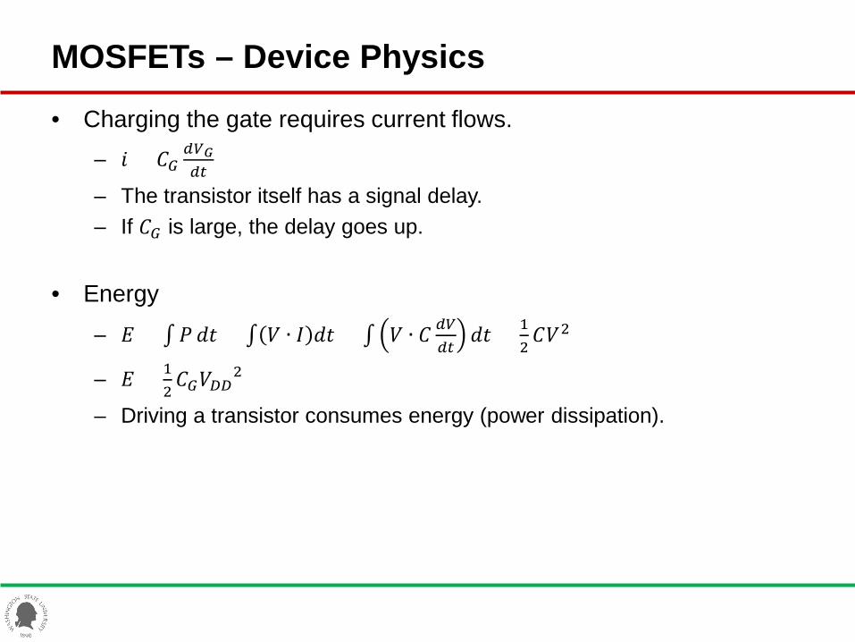
• Charging the gate requires current flows. – 𝑖𝑖 = 𝐶𝐶𝐺𝐺
𝑑𝑑𝑉𝑉𝐺𝐺𝑑𝑑𝑡𝑡
– The transistor itself has a signal delay. – If 𝐶𝐶𝐺𝐺 is large, the delay goes up.
• Energy
– 𝐸𝐸 = ∫𝑃𝑃 𝑑𝑑𝑡𝑡 = ∫ 𝑉𝑉 ∙ 𝐼𝐼 𝑑𝑑𝑡𝑡 = ∫ 𝑉𝑉 ∙ 𝐶𝐶 𝑑𝑑𝑉𝑉𝑑𝑑𝑡𝑡
𝑑𝑑𝑡𝑡 = 12𝐶𝐶𝑉𝑉2
– 𝐸𝐸 = 12𝐶𝐶𝐺𝐺𝑉𝑉𝐷𝐷𝐷𝐷2
– Driving a transistor consumes energy (power dissipation).