piezoelectric response of lead titanate as a function of · pdf filepiezoelectric response of...
TRANSCRIPT

Piezoelectric response of Lead Titanate as a
function of size
Master thesis by
Yizhi Wu
Zernike Institute, University of Groningen Group: Solid state materials for electronics Supervisors: Prof. dr. Beatriz Noheda Drs. Oleksiy Nesterov Period: September 2010-July 2011

2
Abstract In this project, the size effect of ferroelectric PbTiO3 (PTO) thin films is investigated. The piezoelectric coefficient d33 describes the linear relationship between the vertical deformation of a piezoelectric crystal and the external electric field. The theoretical analysis predicted that the d33 increases with decreasing lateral sizes of the PTO thin film due to the release of the clamping to the substrate. In this project, the PTO thin film was fabricated into ~1µm islands and the piezoelectric response was measured. The PTO samples are prepared by Pulsed Laser Depostion (PLD), upon a SrRuO3 (SRO) bottom electrode and a DyScO3 (DSO) substrate. The PTO films are [001] oriented single crystals, with a thichness of 30nm. The PTO islands are designed by Electron Beam Lithography (EBL) and etched by buffered HF (BHF). The 30nm PTO films were successfully etched, with the lateral sizes ranging from 5×5µm2 to 0.5×0.5µm2. The topography measured by Atomic Force Microscopy (AFM) showed that the PTO islands were in good shape. The ferroelectric polarization could be switched by Piezoelectric Force Microscopy (PFM). The piezoelectric hysteresis loop measured by PFM demonstrated that the piezoelectric coefficient d33 increases with decreasing lateral sizes, in a good agreement with the theoretical prediction.

3
Contents
Abstract…………………………………………………………………….2
Chapter 1: Background knowledge 1.1 Ferroelectricity………………………………………………………………………...4 1.2 Phase transition of ferroelectrics………………………………………………………5 1.3 Piezoelectricity………………………………………………………………………...6 1.4 Piezoelectric coefficient……………………………………………………………….7 1.5 PZT ferroelectric thin film…………………………………………………………….8 1.6 Morphotropic phase boundary………………………………………………………...9 1.7 Lattice strain………………………………………………………………………….11 1.8 Ferroelectric domains………………………………………………………………...11 1.9 Size effect…………………………………………………………………………….13
Chapter 2: Experimental procedures 2.1 Device structure……………………………………………………………………...16 2.2 Fabrication process of PTO devices…………………………………………………17 2.3 Pulsed laser deposition……………………………………………………………….18 2.4 Electron beam lithography…………………………………………………………...19 2.5 Atomic force microscopy…………………………………………………………….21 2.6 Piezoelectric Force Microscopy……………………………………………………...22
Chapter 3 Experimental results 3.1 Tip effect……………………………………………………………………………..26 3.2 Results of the positive photoresist…………………………………………………...28 3.3 Results of the negative photoresist…………………………………………………..32 3.4 Ferroelectric property of the PTO islands……………………………………………38 3.5 Piezoelectric hysteresis loops………………………………………………………..40
Conclusion…………………………………………………………………43
Improvement and future plan……………………………………………44
Acknowledgements………………………………………………………..45
Appendix…………………………………………………………………..46

4
Chapter 1 Background knowledge This chapter serves as an introduction to the concepts of ferroelectrics and PbTiO3 thin films. It starts with the explanation of the features of ferroelectricity, followed by the theoretical explanation of the ferroelectric phase transition with the method of the Ginzburg-Landau theory. After that, the piezoelectric is explained along with the definition of the piezoelectric coefficient. Then, the PbTiO3 thin film is introduced, with its Morphotropic Phase Boundary (MPB), domain structures and the size effect. 1.1 Ferroelectricity Ferroelectricity is a property of materials which display a spontaneous polarization without an external electric field. Ferroelectric materials perform piezoelectric and pyroelectric behaviors as well. The polarization means the electric dipole moment per volume. The total polarization of ferroelectric materials consists of two parts: a spontaneous polarization Ps and the polarization due to the external electric field PE. Therefore, the electric displacement field D accounts both effects, and is described as D=PE+Ps=ε0εrE+Ps, where εr is the dielectric constant. Moreover, the permanent polarization of ferroelectric materials can be switched by an external electric field. The polarization behaviors of materials can be separated into three types: dielectricity, paraelectricity, and ferroelectricity. Materials are called dielectrics, if the polarization is linearly to the external electric field. Most materials are dielectrics and the electric permittivity is constant in this case. If the polarization is nonlinear, it is called paraelectricity, shown in Fig. 1. Compared to the dielectricity and the paraelectricity, the distinguishing feature of ferroelectricity is that the spontaneous polarization can be changed by an external electric field, as a result of a hysteresis loop. In the nonlinear part of the ferroelectric hysteresis loop, the domain with its polarization direction converse to the external electric field is switched to the direction parallel to the field. In the linear part, all domains have the same polarization direction as the electric field. At a zero field, the value of polarization is called remnant polarization Pr.
Fig. 1 Three types of a polarization response with an external electric field: (a) dielectricity, (b) paraelectricity, (c) ferroelectricity. Ferroelectricity is a subclass of pyroelectricity and piezoelectricity. Pyroelectricity was discovered since IV century BC [1] in Tourmaline, and piezoelectricity was known in 1880 in Rochelle salt [2]. Ferroelectricity was defined much later, in 1920 [3, 4]. Valasek suggested the name of ferroelectricity from ferromagnetics, when he investigated the properties of Rochelle salt. Perovskite crystals found the home in ferroelectrics since the discovery of barium titanate in 1940. In 1952, lead zirconate titanate was discovered by Takagi and Shirane [5]. Since then, PZT was and is one of the hottest topics in the research of ferroelectrics. In modern electrical industries, the applications of ferroelectric materials are versatile. The nonlinear feature of ferroelectric materials is utilized in capacitors with tunable capacitance. Ferroelectric random access memory (FeRAM) is one of the alternative non-volatile memory technologies. FeRAM shows excellent features of the low power usage and the fast write performance, which are excellent advantages compared to dielectric RAM (DRAMs). Ferroelectric tunnel junction (FTJ) is another promising
5
application, in which ferroelectric films are fabricated between two metal electrodes [6, 7]. Moreover, the Giant electroresistance (GER) is investigated using ferroelectric thin films [8]. 1.2 Phase transition of ferroelectrics The spontaneous polarization of ferroelectrics disappears above a certain temperature Tc, which is called Critical Temperature. For example, the critical temperature Tc of lead titanate is 490°C. During this solid state phase transition, materials change from the ferroelectric phase in the low temperature to the dielectric phase in high temperature. Ferroelectric crystals show some domain structures within one phase. The mechanism of the ferroelectric phase transition is still under discussion. The ferroelectric phase transition can be divided into two types: the displacive transition and the order-disorder transition. Some phase transitions belong to both types. As for the displacive transition, the ferroelectric state is a result of the competition between two forces within the unit cell. If there is a slight displacement of the ion from the central symmetrical position of the unit cell, the local electric fields is lager than the elastic-restoring force. As a result, the ion shifts to an asymmetrical but equilibrium position, which leads to a permanent dipole. At the temperature above Tc, the central symmetrical is favorable. Therefore, there is no displacement of ions in the unit cell and no macroscopic dipole moment exists. For example, the transition of barium titanate is of the displacive type. In the case of lead titanate, the mechanism is similar but more complicate. As for the order-disorder transition, permanent dipoles exist in both low and high temperature states. Upon the Tc, dipole moments are in random directions. Therefore, there is no macroscopic electric dipole moment. While at the temperature below Tc, dipoles in one domain prefers an identical orientation, which leads to a macroscopic dipole moment. The ferroelectric phase transition of bulk lead titanate is a first-order phase transition. Two coexistent phases can be observed around the transition temperature and the latent heat can be measured during the transition. Moreover, in the first-order phase transition, the nucleation and the growth of one phase take place and expand into the other phase. Based on the Ginzburg-Landau theory, the Gibbs free energy G is expressed as a function of an order parameter P, as G(P). Due to the symmetry of the order parameter, G(P)=G(-P), only the even power stems can exist in the expression. Since the Gibbs free energy G depends on the external electric field E and the temperature T, the expression is given as:
2 4 60 2 4 6
1 1 1( , , ) ...
2 4 6G P E T G E P a P a P a P= − ⋅ + + + +
where the coefficient a6 is positive and the higher terms can be neglected. In the case of no external electric field, the equation can be simplified as:
2 4 60 2 4 6
1 1 1( , )
2 4 6G P T G a P a P a P= + + +
a2 is a temperature-dependent parameter, and is expressed as:
2 , ( 0)c
c
T Ta c c
T
−= ⋅ >
where Tc is the phase transition temperature, and the coefficient c is positive. Since the ferroelectric phase transition of bulk PbTiO3 is first-order, the coefficient a4 is negative and a6 is positive. The Gibbs free energy has a shape of a double-well potential. When P=±Ps, the free energy reaches minimum. The derivative of the free energy is zero at P=±Ps:
2 42 4 6( ) 0
GP a a P a P
P
∂= + + =
∂
P=0 is the trivial solution for paraelectric phase. Thus, the solution of the previous equation is:
( )2 24 4 2 6
6
14
2sP a a a a
a= − ± −
Since the Gibbs free energy reaches the minimum at P=±Ps, the second derivative of the free energy should be positive:

6
22 4
2 4 623 5 0
Ga a P a P
P
∂= + + >
∂
The solution is 2 4
62s
aP
a> − . Therefore, the spontaneous polarization is expressed as:
244 2 6
6
42s
aP a a a
a= − + −
The solution shows the value of the spontaneous polarization of the ferroelectrics below Tc. The directions of the polarization can be converse, which means that there are two equivalent states P=±Ps. For example, in PbTiO3, the direction of spontaneous polarization is along the [001] lattice axis, with a value of 0.75C/m2, as presented in Fig. 2. In Fig. 2, the Gibbs free energy reaches the minimum value at P=±Ps. Above Tc, these two states merge together at P=0, and the material change into the paraelectric state.
Fig. 2 The schematic curve of the Gibbs free energy as a function of the polarization of the perovskite PbTiO3. 1.3 Piezoelectricity Piezoelectricity is a property of materials which accumulate charges under external stress. The piezoelectric effect is a linear electromechanical interaction between the electrical distribution and the strain. Materials which exhibit the direct piezoelectric effect also display the reverse piezoelectric effect. The direct piezoelectric effect means that internal electrical charges accumulate when an external mechanical force is applied. While the converse direct piezoelectric effect means that a mechanical deformation of crystals occurs under an external electric field. For example, for lead zirconate titanate, the piezoelectricity can be measured when the deformation is about 0.1% in dimension. Conversely, the crystal deforms about 0.1% in dimension when an electric field is applied. The discovery of piezoelectric effect was in 1880 by Pierre Curie and Jacques Curie [2]. At that time, quartz and Rochelle salt displayed the piezoelectricity. One year later, the converse piezoelectric effect was deduced mathematically by Gabriel Lippmann, with the thermodynamic principle. Until 1910, piezoelectric crystals were characterized into 20 classes, and piezoelectric coefficients were analyzed. One of the applications of piezoelectric devices in history was sonar, which was applied to ultrasonic submarine detectors in 1917. The application of the ultrasonic transducer made the measurement of viscosity and elasticity in fluids and solids easier, which contributed to the development of material research. During the World War II man-made piezoelectric materials developed, and exhibited a higher
7
piezoelectric response than natural materials. Since then, lead zirconate titanate was brought into hot researches. In crystals, the orientation of the dipole moment lies along the polar axis, which is a high symmetry direction. Crystals can be classified into 32 types according to the symmetry of the unit cells. Among those classes, 11 classes have a centre symmetry, which implies that the no electric dipoles can exist in the unit cell. While in the rest 21 classes of non-centre symmetry, 20 of them exhibit the piezoelectricity, since the absence of the centre symmetry makes the dipole polarization possible. Among these 20 piezoelectric classes, 10 of them can present the spontaneous polarization, as so-called ferroelectricity. For the ferroelectric crystals, the polarizations exist without an external mechanical force. For the piezoelectric-only crystals, the polarizations appear under the external stress. The mechanism can be simply explained as [9]: When a mechanical stress is applied, the structure of piezoelectric crystals changes from piezoelectric-only symmetry to the ferroelectric symmetry, and the latter exhibits a lower symmetry than the former, which makes the polarization possible. 1.4 Piezoelectric coefficient Since the piezoelectric effect is the interaction between the mechanical deformation and the electric field, the piezoelectric coefficient is one of the most important parameters during the investigation. The linear relationship between the external mechanical stress Tjk and the resulting electric charge density Di , as known as the direct piezoelectric effect, can be presented as[10]:
i ijk jkD d T= ⋅
where Tjk is a second-rank stress tensor, and dijk is the third-rank piezoelectric coefficient with a unit of C/N. Conversely, the converse piezoelectric effect, which describes the deformation of crystals under external an electric field, can be written as:
T
jk ijk ix d E= ⋅
where the xjk is a second-rank stain, Ei is the applied electric field, and the dijk is the converse piezoelectric coefficient, with a unit of m/V. The superscript T stands for the transposition of the matrix. Based on thermal dynamical reasons [11], the coefficients ddirenct=dconverse. Moreover, because the strain and the stress are both symmetrical tensors, there is a relationship between the indices of the piezoelectric coefficients: dijk=dikj. The elements of the coefficient can be further simplified due to the symmetry of crystals. Commonly, the direct and converse piezoelectric effects can be expressed as:
1
21 15
32 24
431 32 333
5
6
0 0 0 0 0
0 0 0 0 0
0 0 0
T
TD d
TD d
Td d dD
T
T
=
&
1 31
2 321
3 332
4 243
5 15
6
0 0
0 0
0 0
0 0
0 0
0 0 0
s d
s dE
s dE
s dE
s d
s
=
In practice, the measurement of the piezoelectric coefficient is carried out in this way: a DC voltage normal to the thin film surface is applied through a electrode, and the deformation of the thin film is measured along the same direction at the mean time. In this case, the piezoelectric coefficient measured is called the longitudinal piezoelectric coefficient dzz. The two subscripts “zz” stand for the directions of the electric field and the deformation respectively. In the tetragonal symmetry group (4mm), this coefficient can be expressed as [11, 12]:
2 331 15 33( )sin cos cos
zzd d d dθ θ θ= + +
where θ is the angle between the measurement direction and the [001] crystal axis. In our PFM measurement, the direction of [001] axis is normal to the thin film, which means that θ=0 in this case. Therefore, the longitudinal piezoelectric coefficients dzz and the d33 are identical.
8
The behavior of the strain versus the electric field is in a shape of butterfly loop (Fig. 3). Ideally, the deformation is linear to the electric field and the shape is due to three types of effects: the converse piezoelectric effect; the switching of domain walls; the movement of domain walls. At the zero field (Point A in fig. 3(a)), the strain is zero. As the electric field increases (A to C), the crystal deforms linearly with the external field. When the electric field decreases (C to D), the polarization changes by180° at the coercive electric field (Point D). After switching, the polarization is parallel to the electric field and the strain is positive again (Point E). And then, the strain behaves linearly against the electric field again. In the real case, the shape of the loop is more complicated, as presented in Fig. 3(b). The value of the piezoelectric coefficient is calculated from the slope of the linear part.
Fig. 3 (a) the ideal loop of the strain versus the electric field; (b) the actual butterfly loop. 1.5 PZT ferroelectric thin film Lead Zirconate Titanate (Pb[ZrxTi1-x]O3, 0≤x≤1) is a ternary oxide, and a solid solution of lead zirconate and lead titanate. PZT exhibits high piezoelectric and ferroelectric properties and has been investigated for decades. PZT was discovered by Yutaka Takagi, Gen Shirane and Etsuro Sawaguchi in 1952. Based on the piezoelectric feature, PZT is widely used to make ultrasound transducers and actuators in large variety of technological and micro-electromechanical systems (MEMS) applications [13]. PZT is usually doped with acceptors (p-type) or donors (n-type) in commercial applications. In the case of p-PZT, the domain wall is pinned by the impurities and the piezoelectric coefficient is lower. In the case of n-PZT, the piezoelectric coefficient is higher, with a larger losses of the materials due to internal friction. The piezoelectric coefficient of PZT ranges from 100pm/V to 800pm/V depending on the treatment and doping [14]. In the Titanium rich region, PZT shows the tetragonal or cubic structures, as presented in Fig 4. The ferroelectric phase transition temperature Tc of PZT is around 500°C. In the case of bulk lead titanate (when x=0 in Pb[ZrxTi1-x]O3), the transition temperature is 490°C. Below Tc, PZT is in the ferroelectric tetragonal phase with the spontaneous polarization along the c axis of the unit cell. Above Tc, PZT is in the paraelectric cubic phase. The displacement of the central cation Ti4+ or Zr4+ is the origin of the spontaneous polarization. Such displacement is the result of the balance between two different forces: the long-range coulomb force and the short-range repulsive force. The coulomb force prefers the paraelectric state while the repulsive forces prefers the ferroelectric state [15]. The ferroelectric phase transition of lead titanate (PTO) is the first order phase transition, which means that the transition is abrupt and two phases can be coexistent during the transition. While in PTO films, this phase transition can shift to the second order phase transition [16] due to the lattice strain.
9
Fig. 4 The schematic representation of the unit cell structure of PZT: cubic (left) and tetragonal (right). Bulk PZT is tetragonal below Tc and cubic above Tc. In the cubic phase, the lattice parameter a is indicated. In the tetragonal phase, the tetragonal parameters a and c, and the spontaneous polarization P are indicated. 1.6 Morphotropic phase boundary The phase transition can be induced not only by the change of temperature, but also by the displacement of homovalent cations with different sizes, which gives rise to so-called “chemical pressure”. The solid solution PZT is a mixture of ferroelectric tetragonal (FT) PbTiO3 and rhombohedral (FR) PbZrO3, as presented in Fig. 2. The phase transition from one crystal phase to another takes place at a composition of PbZr0.48Ti0.52O3 (x=0.48), corresponding to the “Morphotropic Phase Boundary” (MPB). Generally, the MPB is a vertical or nearly vertical line in the terperauter-x diagrams, where x can be composition, electric field, etc [17].
Fig. 5 The phase diagram of lead zirconate titanate [18]. At the low temperature, the structure of PZT is rhombohedral in the zirconium-rich region and tetragonal in the titanium-rich region. At the high temperature, the structure is cubic. The morphotropic phase boundary is at the composition of x=0.48. The notations FR(HT) and FR(LT) stand for rhombohedral structures at the high temperature and at the low temperature respectively, which belong to different space groups.

10
A giant piezoelectric effect can be observed at the morphotropic phase boundary, and has attracted considerable interest for many years. The piezoelectric constant at the MPB is extremely large [13]. The piezoelectric coefficient reaches the maximum at the MPB in both theoretical [17] and experimental [19] researches. This phenomenon is still under a lively research. The giant piezoelectric effect can be explained by the rotation of the spontaneous polarization [20]. Near the phase boundary, the free energies of the rhombohedral state and the tetragonal state are equivalent, which increases the number of allowable polarization directions. The allowable polarization directions depend on the symmetry of the crystal. The possible directions of the spontaneous polarization in some crystal structures related in this project are listed below:
Crystal Structure Polarization Component Direction of Polarization Cubic P1=P2=P3=0 None Tetragonal P1=P2=0, P3≠0 [001] Rhombohedral P1=P2=P3≠0 [111] Monoclinic P1=P2≠0; P3≠0; P1≠P3 in (110) plane
In the tetragonal structure, there are 6 possible directions of the polarization; while in the rhombohedral structure, there are 8 possible directions. At the MPB, these directions are equally favorable energetically. Thereby there are 14 possible directions in total, which leads to a larger freedom of the polarization. Near the MPB, a two-phase coexistence was proposed to explain the giant piezoelectric effect [20] in 1993. In 1999, a new monoclinic phase of PZT at the MPB was discovered with the method of X-ray synchrotron powder diffraction by B.Noheda [21]. Additionally, a second monoclinic phase at the lower temperature was found with the neutron diffraction in 2002 [22]. Until recently, a coexistence of rhombohedral and monoclinic phases is observed at x=0.460 with the method of the neutron diffraction [23]. All discoveries come to the same explanation: the direction of the spontaneous polarization changes continuously or discontinuously with the change of the composition [24], as shown in Fig. 6. In fig. 6, the directions of the polarization in tetragonal (P4mm) and rhombohedral (R3m) phases are [001] and [111] respectively. While in the monoclinic phase, the symmetry element of the space group Cm is a mirror plane, which is the only comment element between the tetragonal and rhombohedral phases. When the composition of titanium increases, the phase transition takes place at the MPB. During this process, the polarization rotates from [001] to [111] through the (110) plane, which is the polarization region of the monoclinic phase [25]. Theoretical researches also contribute to the explanation of the giant piezoelectric effect [26]. Close to the MPB, the flattening of the Gibbs free energy occurs, leading the increase of the dielectric constant, since the dielectric constant is inversely proportional to the first derivative of the Gibbs free energy.
Fig. 6 The rotation of the polarization from the tetragonal phase to the rhombohedral phase.
11
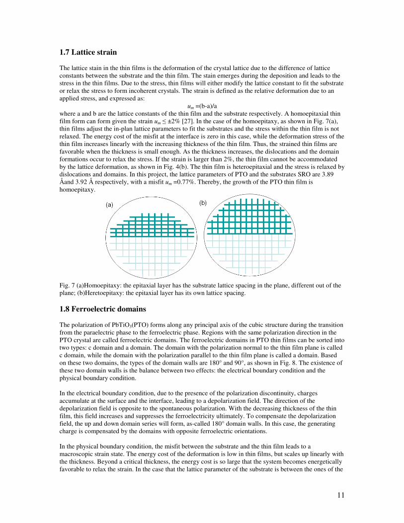
1.7 Lattice strain The lattice stain in the thin films is the deformation of the crystal lattice due to the difference of lattice constants between the substrate and the thin film. The stain emerges during the deposition and leads to the stress in the thin films. Due to the stress, thin films will either modify the lattice constant to fit the substrate or relax the stress to form incoherent crystals. The strain is defined as the relative deformation due to an applied stress, and expressed as:
um =(b-a)/a where a and b are the lattice constants of the thin film and the substrate respectively. A homoepitaxial thin film form can form given the strain um ≤ ±2% [27]. In the case of the homoepitaxy, as shown in Fig. 7(a), thin films adjust the in-plan lattice parameters to fit the substrates and the stress within the thin film is not relaxed. The energy cost of the misfit at the interface is zero in this case, while the deformation stress of the thin film increases linearly with the increasing thickness of the thin film. Thus, the strained thin films are favorable when the thickness is small enough. As the thickness increases, the dislocations and the domain formations occur to relax the stress. If the strain is larger than 2%, the thin film cannot be accommodated by the lattice deformation, as shown in Fig. 4(b). The thin film is heteroepitaxial and the stress is relaxed by dislocations and domains. In this project, the lattice parameters of PTO and the substrates SRO are 3.89 Åand 3.92 Å respectively, with a misfit um =0.77%. Thereby, the growth of the PTO thin film is homoepitaxy.
Fig. 7 (a)Homoepitaxy: the epitaxial layer has the substrate lattice spacing in the plane, different out of the plane; (b)Heretoepitaxy: the epitaxial layer has its own lattice spacing. 1.8 Ferroelectric domains The polarization of PbTiO3(PTO) forms along any principal axis of the cubic structure during the transition from the paraelectric phase to the ferroelectric phase. Regions with the same polarization direction in the PTO crystal are called ferroelectric domains. The ferroelectric domains in PTO thin films can be sorted into two types: c domain and a domain. The domain with the polarization normal to the thin film plane is called c domain, while the domain with the polarization parallel to the thin film plane is called a domain. Based on these two domains, the types of the domain walls are 180° and 90°, as shown in Fig. 8. The existence of these two domain walls is the balance between two effects: the electrical boundary condition and the physical boundary condition. In the electrical boundary condition, due to the presence of the polarization discontinuity, charges accumulate at the surface and the interface, leading to a depolarization field. The direction of the depolarization field is opposite to the spontaneous polarization. With the decreasing thickness of the thin film, this field increases and suppresses the ferroelectricity ultimately. To compensate the depolarization field, the up and down domain series will form, as-called 180° domain walls. In this case, the generating charge is compensated by the domains with opposite ferroelectric orientations. In the physical boundary condition, the misfit between the substrate and the thin film leads to a macroscopic strain state. The energy cost of the deformation is low in thin films, but scales up linearly with the thickness. Beyond a critical thickness, the energy cost is so large that the system becomes energetically favorable to relax the strain. In the case that the lattice parameter of the substrate is between the ones of the

12
thin film (a<as<c), the thin film will form a series of domains with alternative a/c orientations, as called 90° domain structure.
Fig. 8 The formation of 180° and 90° domain walls in PTO during the ferroelectric phase transition. aC, aT, cT stand for the lattice parameters, and the notations C and T mean the cubic phase and tetragonal phase respectively. Ps stands for polarization within the films. In the case of the PbTiO3 film on the SrRuO3 substrate, the condition a<as<c is filled. Thus, both 180° and 90° domain structures are possible on the PTO films. The energy cost of the depolarizing field decreases with increasing film thickness, while the cost of the lattice deformation scales up linearly with the thickness. Therefore, a critical thickness exists on the PbTiO3/SrRuO3 structure, above which a/c domain structure is favorable and below which alternative a/c domain structure is favorable. The a/c domain series has been demonstrated experimentally, as shown in Fig. 9. An alternative a/c domain was measured with a periodic length of 27nm. As explained before, the existence of a domains is to compensate the mismatch of the lattice parameters. The ratio between a and c domains can be expressed simply as: Nac+Nca=Nas, where Na and Nc stand for the numbers of unit cells in a and c domain respectively, and N is the number of the total unit cells. Thus, the faction of the a domain is Na/N=(as-a)/(a-c)≈0.20, in a good agreement with the experiment result. In this project, the piezoelectric coefficient is measured in the direction normal to the thin film, which means that only the c domains contribute to the piezoelectric response.
Fig. 9 A TEM image of a 30nm thick film of PbTiO3 with a SrRuO3 buffer layer on DyscO3 substrate [28]. A domain walls separate two different-oriented domains. Domain walls can be sorted into two types [29]: the ferroelectric domain and the ferroelastic domain. The ferroelectric domain differs in orientation to the spontaneous polarization vector, while the ferroelastic domain differs in orientation to the spontaneous strain tensor. In PTO, the 180° domain walls are ferroelectric while the 90° domain walls are both ferroelectric and ferroelastic. The structure of domain walls in PTO is shown in Fig. 10. Normally, the
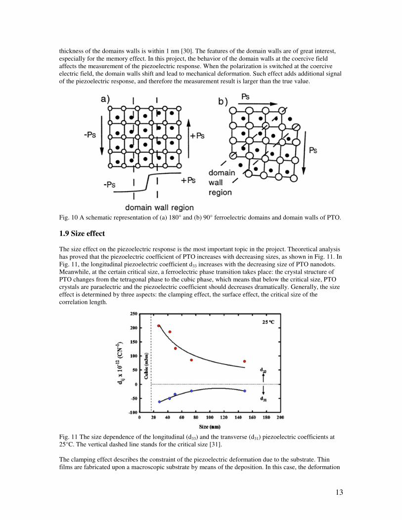
13
thickness of the domains walls is within 1 nm [30]. The features of the domain walls are of great interest, especially for the memory effect. In this project, the behavior of the domain walls at the coercive field affects the measurement of the piezoelectric response. When the polarization is switched at the coercive electric field, the domain walls shift and lead to mechanical deformation. Such effect adds additional signal of the piezoelectric response, and therefore the measurement result is larger than the true value.
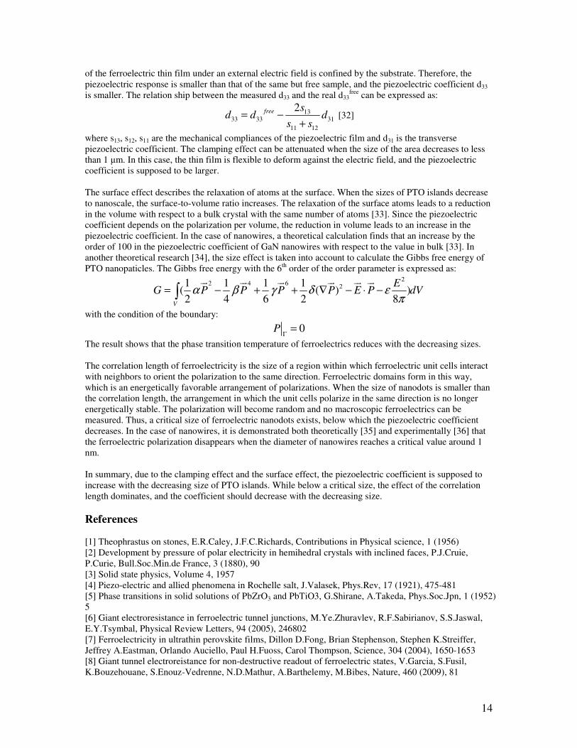
Fig. 10 A schematic representation of (a) 180° and (b) 90° ferroelectric domains and domain walls of PTO. 1.9 Size effect The size effect on the piezoelectric response is the most important topic in the project. Theoretical analysis has proved that the piezoelectric coefficient of PTO increases with decreasing sizes, as shown in Fig. 11. In Fig. 11, the longitudinal piezoelectric coefficient d33 increases with the decreasing size of PTO nanodots. Meanwhile, at the certain critical size, a ferroelectric phase transition takes place: the crystal structure of PTO changes from the tetragonal phase to the cubic phase, which means that below the critical size, PTO crystals are paraelectric and the piezoelectric coefficient should decreases dramatically. Generally, the size effect is determined by three aspects: the clamping effect, the surface effect, the critical size of the correlation length.
Fig. 11 The size dependence of the longitudinal (d33) and the transverse (d31) piezoelectric coefficients at 25°C. The vertical dashed line stands for the critical size [31]. The clamping effect describes the constraint of the piezoelectric deformation due to the substrate. Thin films are fabricated upon a macroscopic substrate by means of the deposition. In this case, the deformation
14
of the ferroelectric thin film under an external electric field is confined by the substrate. Therefore, the piezoelectric response is smaller than that of the same but free sample, and the piezoelectric coefficient d33 is smaller. The relation ship between the measured d33 and the real d33
free can be expressed as:
1333 33 31
11 12
2free sd d d
s s= −
+ [32]
where s13, s12, s11 are the mechanical compliances of the piezoelectric film and d31 is the transverse piezoelectric coefficient. The clamping effect can be attenuated when the size of the area decreases to less than 1 µm. In this case, the thin film is flexible to deform against the electric field, and the piezoelectric coefficient is supposed to be larger. The surface effect describes the relaxation of atoms at the surface. When the sizes of PTO islands decrease to nanoscale, the surface-to-volume ratio increases. The relaxation of the surface atoms leads to a reduction in the volume with respect to a bulk crystal with the same number of atoms [33]. Since the piezoelectric coefficient depends on the polarization per volume, the reduction in volume leads to an increase in the piezoelectric coefficient. In the case of nanowires, a theoretical calculation finds that an increase by the order of 100 in the piezoelectric coefficient of GaN nanowires with respect to the value in bulk [33]. In another theoretical research [34], the size effect is taken into account to calculate the Gibbs free energy of PTO nanopaticles. The Gibbs free energy with the 6th order of the order parameter is expressed as:
22 4 6 21 1 1 1
( ( ) )2 4 6 2 8
V
EG P P P P E P dVα β γ δ ε
π= − + + ∇ − ⋅ −∫
ur ur ur ur ur ur
with the condition of the boundary:
0PΓ
=
The result shows that the phase transition temperature of ferroelectrics reduces with the decreasing sizes. The correlation length of ferroelectricity is the size of a region within which ferroelectric unit cells interact with neighbors to orient the polarization to the same direction. Ferroelectric domains form in this way, which is an energetically favorable arrangement of polarizations. When the size of nanodots is smaller than the correlation length, the arrangement in which the unit cells polarize in the same direction is no longer energetically stable. The polarization will become random and no macroscopic ferroelectrics can be measured. Thus, a critical size of ferroelectric nanodots exists, below which the piezoelectric coefficient decreases. In the case of nanowires, it is demonstrated both theoretically [35] and experimentally [36] that the ferroelectric polarization disappears when the diameter of nanowires reaches a critical value around 1 nm. In summary, due to the clamping effect and the surface effect, the piezoelectric coefficient is supposed to increase with the decreasing size of PTO islands. While below a critical size, the effect of the correlation length dominates, and the coefficient should decrease with the decreasing size. References [1] Theophrastus on stones, E.R.Caley, J.F.C.Richards, Contributions in Physical science, 1 (1956) [2] Development by pressure of polar electricity in hemihedral crystals with inclined faces, P.J.Cruie, P.Curie, Bull.Soc.Min.de France, 3 (1880), 90 [3] Solid state physics, Volume 4, 1957 [4] Piezo-electric and allied phenomena in Rochelle salt, J.Valasek, Phys.Rev, 17 (1921), 475-481 [5] Phase transitions in solid solutions of PbZrO3 and PbTiO3, G.Shirane, A.Takeda, Phys.Soc.Jpn, 1 (1952) 5 [6] Giant electroresistance in ferroelectric tunnel junctions, M.Ye.Zhuravlev, R.F.Sabirianov, S.S.Jaswal, E.Y.Tsymbal, Physical Review Letters, 94 (2005), 246802 [7] Ferroelectricity in ultrathin perovskite films, Dillon D.Fong, Brian Stephenson, Stephen K.Streiffer, Jeffrey A.Eastman, Orlando Auciello, Paul H.Fuoss, Carol Thompson, Science, 304 (2004), 1650-1653 [8] Giant tunnel electroreistance for non-destructive readout of ferroelectric states, V.Garcia, S.Fusil, K.Bouzehouane, S.Enouz-Vedrenne, N.D.Mathur, A.Barthelemy, M.Bibes, Nature, 460 (2009), 81
15
[9] Crystal-field induced dipoles in heteropolar crystals I:concept, Mario Birkholz, Z.Phys.B, 96 (1995), 325-332 [10] Ferroelectric, dielectric and piezoelectric properties of ferroelectric thin films and ceramics, Dragan Damjanovic, Rep.Prog.Phys. 61 (1998), 1267-1324 [11] Piezoelectric scanning force microscopy: what quantitative information can we really get out of piezoresponse measurements on ferroelectric thin film, Catalin Harnagea, Alain Pignolet, Martin Alexe, Dietrich Hesse, Integrated Ferroelectrics, 44 (2002), 113-124 [12] Finite-Temperature properties of Pb(Zr1-xTix)O3 Alloys from first principles, L.Bellaiche, Alberto Gracia, David Vanderbilt, Phys.Rev.Letts. 84 (2000), 5427-5430 [13] Pressure tuning of the morphotropic phase boundary in piezoelectric lead zirconate titanate, J.Rouquette, J.Haines, V.Bornand, M.Pintard, Ph.Papet, et al, Physical Review B, 70 (2004), 014108 [14] http://www.piezotechnologies.com/materialssheet.htm [15] Origin of ferroelectricity in perovskite oxides, R.E.Cohen, Nature, 385 (1992), 136-138 [16] High-pressure Raman study of zone-center phonons in PbTiO3, J.A.Sanjurjo, E.Lopez-Cruz, Gerald Burns, Physical Review B 28 (1983), 7260-7268 [17] Effects of tricritical points and morphotropic phase boundaries on t he piezoelectric properties of ferroelectrics, Marcel Porta, Turab Lookman, Physical Review B 83 (2011), 174108 [18] Piezoelectric ceramics, B.Jaffe, W.R.Cook, and H.Jaffe, Academic London, 1971, p136 [19] Ferroelectric and piezoelectric properties of epitaxial PZT films and devices on silicons, Minh Duc Nguyen, PhD thesis [20] Theoretical model for the morphotropic phase boundary in lead zirconate-lead titanate solid solution, Wenwe Cao, L.Eric Cross, Physical Review B 47 (1993), 4825-4830 [21] A monoclinic ferroelectric phase in the Pb(Zr1-xTix)O3 solid solution, B.Noheda, et.al, Applied Physics Letters, 74 (1999), 2059-2061 [22] Antiferrodistortive phase transition in Pb(Ti0.48Zr0.52)O3: space group of the lowest temperature monoclinic phase, D.M.Hatch, H.T.Stokes, Rajeev Ranjan, Ragini, S.K.Misha, Dhananjai Pandey, Brendan J.Kennedy, Physical Review B 65 (2002), 212101 [23] Single crystal study of competing rhombohedral and monoclinic order in lead zirconate titanate, D.Phelan, X.Long, Y.Xie, Z.-G.Ye, A.M.Glazer, H.Yokota, P.A.Thomas, P.M.Gehring, Physical review letters, 105 (2010), 207601 [24] Polarization rotation mechanism for ultrahigh electromechanical response in single-crystal piezoelectrics, Huaxiang Fu, Ronald E.Cohen, Nature, 403(2000), 281-283 [25] Structrure and high-piezoelectricity in the lead oxide solid solutions, B.Noheda, Current Opinion in Solid State and Materials Science, 6 (2004), 27-34 [26] Contributions to the piezoelectric effect in ferroelectric single crystals and ceramics, Dragan Damjanovic, J.Am.Ceram.Soc, 88 (2005), 2663-2676 [27] Physics of thin film ferroelectric oxides, M.Dawber, K.M.Rabe, J.F.Scott, Reviews of modern physics, 77 (2005), 1083-1130 [28] Smallest 90° domains in epitaxial ferroelectric films, A.H.G.Vlooswijk, B.Noheda, et al, Applied Physics Letters, 91 (2007), 112901 [29] Ferroelectric, dielectric and piezoelectric properties, Dragan Damjanovic, Rep.prog.Phys, 61 (1998), 1267-1324 [30] Principles and applications of ferroelectrics and related materials, M.E.Lines , A.M.Glass, Oxford University Press, (1977), P.525 [31] Thermodynamic theory of intrinsic finite size effects in PbTiO3 nanocrystals II. Dielectric and piezoelectric properties, Journal of Applied Physics, 101 (2007), 064115 [32] Measurement of piezoelectric coefficients of ferroelectric thin films, K.Lefki, G.J.M.Dormans, J.Appl.Phys, 76 (1994), 1764-1767 [33] Giant piezoelectric size effects in zinc oxide and gallium nitride nanowires. A first principles investigation, Ravi Agrawal, Horacio D.Espinosa, Nano Lett, 11 (2011), 7860-790 [34] Modeling of ferroelectric-Dielectric Nanocomposites, V.N.Nechaev, A.V.Shuba, Ferroelectrics, 397 (2010), 32-42 [35] Spontaneous polarization in one-dimensional Pb(ZrTi)O3 nanowires, Ivan I.Naumov, Huaxiang Fu, Physical Review Letters, 95 (2005) 247602 [36] Finite-size effects in BaTiO3 nanowires, Gregory Geneste, Eric Bousquet, Javier Junquera, Philippe Ghosez, Appl.Phys.Lett, 88 (2006), 112906-112908
16
Chapter 2 Experimental procedures This chapter serves as an illustration of the fabrication process of the PbTiO3 devices. The device structures and the parameters are explained first, followed by the fabrication process. In the latter part, the equipment of the fabrication and the measurement are introduced: Plus Laser Deposition (PLD) for the preparation of samples, Electron-beam Lithography (EBL) for the design of the patterns, Atomic Force Microscopy (AFM) for the topography of PTO islands and Piezoelectric Force Microscopy (PFM) for the measurement of ferroelectrics and piezoelectric hysteresis loops. 2.1 Device structure Substrate For the layer-by-layer thin film growth, substrates are required to be both lattice-matched and stable. Silicon (Si) substrates are the most popular one for microelectronics. The advantages of silicon substrates are: the low price, the high surface quality, the good thermal conductivity and the flexibility of processing. However, due to the large misfit of lattice parameters between silicon and PbTiO3, which induces enormous lattice strain during thin film growth, silicon substrates are replaced by DyScO3 (DSO). The lattice parameters of the materials used (except for Si) in the fabrication of ferroelectric devices are listed in Table. 1.
Material Structure a (Å) b (Å) c (Å) Si Cubic 5.43 5.43 5.43 SrRuO3[1] Cubic 3.92 3.92 3.92 DyScO3[2] Cubic 3.95 3.95 3.95 PbTiO3[3] Tetragonal 3.89 3.89 4.14
Table. 1 The lattice parameters of the materials DSO is selected because of the lattice match and chemical compatibility. The electrical properties of the substrates, such as the conductivity and the dielectric constant, play important roles in thin film growth and crystallization. DSO is an insulator, with a band gap of 5.7eV [4]. The dielectric constant along the three crystallographic directions are ε11=22.0, ε22=118.8, ε33=35.5 at room temperature [5]. Other data on the electric properties of DSO are not widely-spread and still under investigation. DSO substrates are provided by CrysTec GmbH. All the substrates were cut into 10×10 mm2 or 5×5 mm2 pieces, and cleaned by ultrasonic cleaning with acetone and ethanol for 20 minutes. A crucial prerequisite of thin film growth is the single termination state of the surface. The termination of the perovskite substrate affects the electronic and chemical properties of the surface and the crystal structure of the upper layers. For ABO3 substrates, the terminated layers can be either AO or BO2 chemical groups, as shown in Fig. 12 [6]. After the annealing, the NaOH etching and the demi water rinsing, the DSO substrate is single terminated.
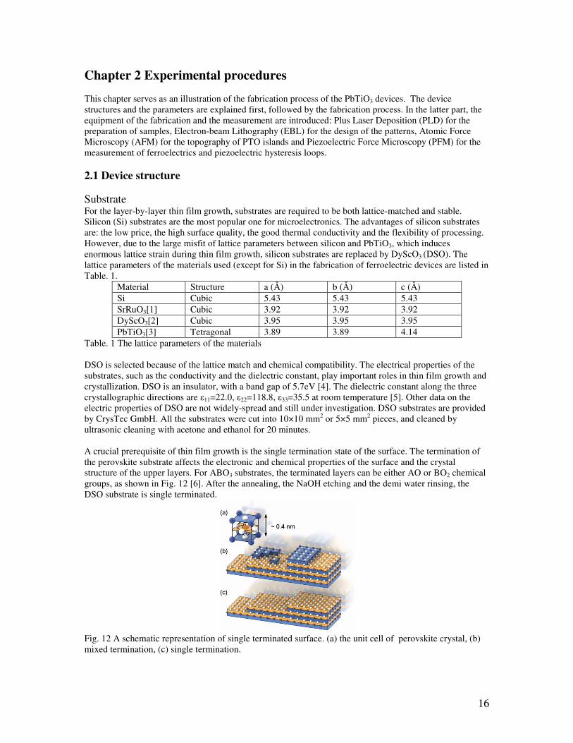
Fig. 12 A schematic representation of single terminated surface. (a) the unit cell of perovskite crystal, (b) mixed termination, (c) single termination.
17
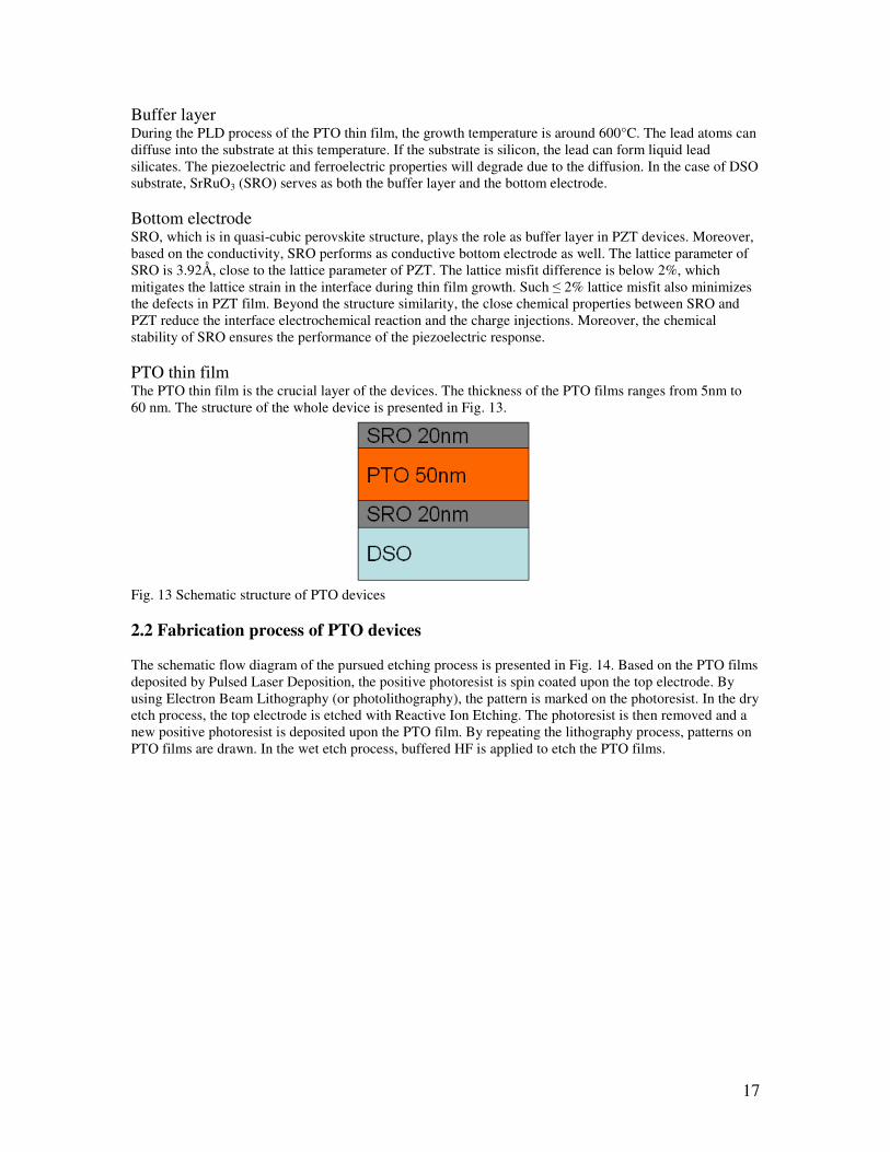
Buffer layer During the PLD process of the PTO thin film, the growth temperature is around 600°C. The lead atoms can diffuse into the substrate at this temperature. If the substrate is silicon, the lead can form liquid lead silicates. The piezoelectric and ferroelectric properties will degrade due to the diffusion. In the case of DSO substrate, SrRuO3 (SRO) serves as both the buffer layer and the bottom electrode. Bottom electrode SRO, which is in quasi-cubic perovskite structure, plays the role as buffer layer in PZT devices. Moreover, based on the conductivity, SRO performs as conductive bottom electrode as well. The lattice parameter of SRO is 3.92Å, close to the lattice parameter of PZT. The lattice misfit difference is below 2%, which mitigates the lattice strain in the interface during thin film growth. Such ≤ 2% lattice misfit also minimizes the defects in PZT film. Beyond the structure similarity, the close chemical properties between SRO and PZT reduce the interface electrochemical reaction and the charge injections. Moreover, the chemical stability of SRO ensures the performance of the piezoelectric response. PTO thin film The PTO thin film is the crucial layer of the devices. The thickness of the PTO films ranges from 5nm to 60 nm. The structure of the whole device is presented in Fig. 13.
Fig. 13 Schematic structure of PTO devices 2.2 Fabrication process of PTO devices The schematic flow diagram of the pursued etching process is presented in Fig. 14. Based on the PTO films deposited by Pulsed Laser Deposition, the positive photoresist is spin coated upon the top electrode. By using Electron Beam Lithography (or photolithography), the pattern is marked on the photoresist. In the dry etch process, the top electrode is etched with Reactive Ion Etching. The photoresist is then removed and a new positive photoresist is deposited upon the PTO film. By repeating the lithography process, patterns on PTO films are drawn. In the wet etch process, buffered HF is applied to etch the PTO films.

18
Fig. 14 The fabrication process of the PTO devices [7]. 2.3 Pulsed laser deposition
19
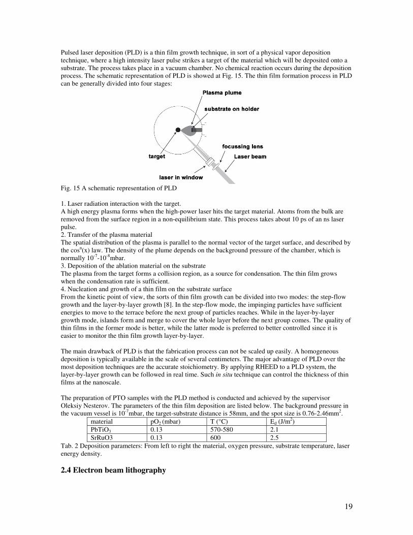
Pulsed laser deposition (PLD) is a thin film growth technique, in sort of a physical vapor deposition technique, where a high intensity laser pulse strikes a target of the material which will be deposited onto a substrate. The process takes place in a vacuum chamber. No chemical reaction occurs during the deposition process. The schematic representation of PLD is showed at Fig. 15. The thin film formation process in PLD can be generally divided into four stages:
Fig. 15 A schematic representation of PLD 1. Laser radiation interaction with the target. A high energy plasma forms when the high-power laser hits the target material. Atoms from the bulk are removed from the surface region in a non-equilibrium state. This process takes about 10 ps of an ns laser pulse. 2. Transfer of the plasma material The spatial distribution of the plasma is parallel to the normal vector of the target surface, and described by the cosn(x) law. The density of the plume depends on the background pressure of the chamber, which is normally 10-7-10-8mbar. 3. Deposition of the ablation material on the substrate The plasma from the target forms a collision region, as a source for condensation. The thin film grows when the condensation rate is sufficient. 4. Nucleation and growth of a thin film on the substrate surface From the kinetic point of view, the sorts of thin film growth can be divided into two modes: the step-flow growth and the layer-by-layer growth [8]. In the step-flow mode, the impinging particles have sufficient energies to move to the terrace before the next group of particles reaches. While in the layer-by-layer growth mode, islands form and merge to cover the whole layer before the next group comes. The quality of thin films in the former mode is better, while the latter mode is preferred to better controlled since it is easier to monitor the thin film growth layer-by-layer. The main drawback of PLD is that the fabrication process can not be scaled up easily. A homogeneous deposition is typically available in the scale of several centimeters. The major advantage of PLD over the most deposition techniques are the accurate stoichiometry. By applying RHEED to a PLD system, the layer-by-layer growth can be followed in real time. Such in situ technique can control the thickness of thin films at the nanoscale. The preparation of PTO samples with the PLD method is conducted and achieved by the supervisor Oleksiy Nesterov. The parameters of the thin film deposition are listed below. The background pressure in the vacuum vessel is 10-7mbar, the target-substrate distance is 58mm, and the spot size is 0.76-2.46mm2.
material pO2 (mbar) T (°C) Ed (J/m2) PbTiO3 0.13 570-580 2.1 SrRuO3 0.13 600 2.5
Tab. 2 Deposition parameters: From left to right the material, oxygen pressure, substrate temperature, laser energy density. 2.4 Electron beam lithography
20
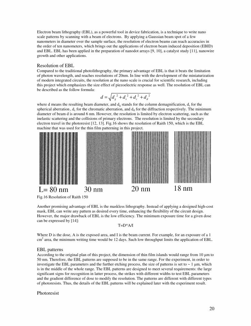
Electron beam lithography (EBL), as a powerful tool in device fabrication, is a technique to write nano scale patterns by scanning with a beam of electrons. By applying a Gaussian beam spot of a few nanometers in diameter over the sample surface, the resolution of electron beams can reach accuracies in the order of ten nanometers, which brings out the applications of electron beam induced deposition (EBID) and EBL. EBL has been applied in the preparation of nanodot arrays [9, 10], a catalyst study [11], nanowire growth and other applications. Resolution of EBL Compared to the traditional photolithography, the primary advantage of EBL is that it beats the limitation of photon wavelength, and reaches resolutions of 20nm. In line with the development of the miniaturization of modern integrated circuits, the resolution at the nano scale is crucial for scientific research, including this project which emphasizes the size effect of piezoelectric response as well. The resolution of EBL can be described as the follow formula:
2 2 2 2g s c d
d d d d d= + + +
where d means the resulting beam diameter, and dg stands for the column demagnification, ds for the spherical aberration , dc for the chromatic aberration, and dd for the diffraction respectively. The minimum diameter of beam d is around 6 nm. However, the resolution is limited by electron scattering, such as the inelastic scattering and the collisions of primary electrons. The resolution is limited by the secondary electron travel in the photoresist [12, 13]. Fig.16 shows the resolution of Raith 150, which is the EBL machine that was used for the thin film patterning in this project.
Fig.16 Resolution of Raith 150 Another promising advantage of EBL is the maskless lithography. Instead of applying a designed high-cost mask, EBL can write any pattern as desired every time, enhancing the flexibility of the circuit design. However, the major drawback of EBL is the low efficiency. The minimum exposure time for a given dose can be expressed by [14]:
T=D*A/I
Where D is the dose, A is the exposed area, and I is the beam current. For example, for an exposure of a 1 cm2 area, the minimum writing time would be 12 days. Such low throughput limits the application of EBL. EBL patterns According to the original plan of this project, the dimension of thin film islands would range from 10 µm to 50 nm. Therefore, the EBL patterns are supposed to be in the same range. For the experiment, in order to investigate the EBL parameters and the further etching process, the size of patterns is set to ~ 1 µm, which is in the middle of the whole range. The EBL patterns are designed to meet several requirements: the large significant signs for recognition in latter process, the strikes with different widths to test EBL parameters and the gradient difference of dose to modify the resolution. The patterns are different with different types of photoresists. Thus, the details of the EBL patterns will be explained later with the experiment result. Photoresist
21
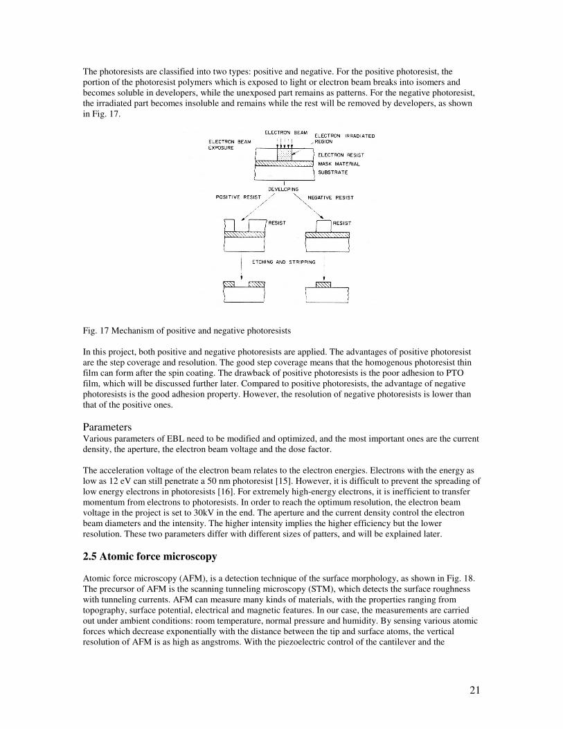
The photoresists are classified into two types: positive and negative. For the positive photoresist, the portion of the photoresist polymers which is exposed to light or electron beam breaks into isomers and becomes soluble in developers, while the unexposed part remains as patterns. For the negative photoresist, the irradiated part becomes insoluble and remains while the rest will be removed by developers, as shown in Fig. 17.
Fig. 17 Mechanism of positive and negative photoresists In this project, both positive and negative photoresists are applied. The advantages of positive photoresist are the step coverage and resolution. The good step coverage means that the homogenous photoresist thin film can form after the spin coating. The drawback of positive photoresists is the poor adhesion to PTO film, which will be discussed further later. Compared to positive photoresists, the advantage of negative photoresists is the good adhesion property. However, the resolution of negative photoresists is lower than that of the positive ones. Parameters Various parameters of EBL need to be modified and optimized, and the most important ones are the current density, the aperture, the electron beam voltage and the dose factor. The acceleration voltage of the electron beam relates to the electron energies. Electrons with the energy as low as 12 eV can still penetrate a 50 nm photoresist [15]. However, it is difficult to prevent the spreading of low energy electrons in photoresists [16]. For extremely high-energy electrons, it is inefficient to transfer momentum from electrons to photoresists. In order to reach the optimum resolution, the electron beam voltage in the project is set to 30kV in the end. The aperture and the current density control the electron beam diameters and the intensity. The higher intensity implies the higher efficiency but the lower resolution. These two parameters differ with different sizes of patters, and will be explained later. 2.5 Atomic force microscopy Atomic force microscopy (AFM), is a detection technique of the surface morphology, as shown in Fig. 18. The precursor of AFM is the scanning tunneling microscopy (STM), which detects the surface roughness with tunneling currents. AFM can measure many kinds of materials, with the properties ranging from topography, surface potential, electrical and magnetic features. In our case, the measurements are carried out under ambient conditions: room temperature, normal pressure and humidity. By sensing various atomic forces which decrease exponentially with the distance between the tip and surface atoms, the vertical resolution of AFM is as high as angstroms. With the piezoelectric control of the cantilever and the
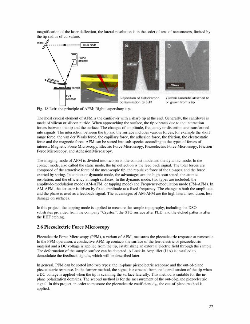
22
magnification of the laser deflection, the lateral resolution is in the order of tens of nanometers, limited by the tip radius of curvature.
Fig. 18 Left: the principle of AFM; Right: supersharp tips The most crucial element of AFM is the cantilever with a sharp tip at the end. Generally, the cantilever is made of silicon or silicon nitride. When approaching the surface, the tip vibrates due to the interaction forces between the tip and the surface. The changes of amplitude, frequency or distortion are transformed into signals. The interaction between the tip and the surface includes various forces, for example the short range force, the van der Waals force, the capillary force, the adhesion force, the friction, the electrostatic force and the magnetic force. AFM can be sorted into sub-species according to the types of forces of interest: Magnetic Force Microscopy, Electric Force Microscopy, Piezoelectric Force Microscopy, Friction Force Microscopy, and Adhesion Microscopy. The imaging mode of AFM is divided into two sorts: the contact mode and the dynamic mode. In the contact mode, also called the static mode, the tip deflection is the feed back signal. The total forces are composed of the attractive force of the mesoscopic tip, the repulsive force of the tip-apex and the force exerted by spring. In contact or dynamic mode, the advantages are the high scan speed, the atomic resolution, and the efficiency at rough surfaces. In the dynamic mode, two types are included: the amplitude-modulation mode (AM-AFM, or tapping mode) and Frequency-modulation mode (FM-AFM). In AM-AFM, the actuator is driven by fixed amplitude at a fixed frequency. The change in both the amplitude and the phase is used as a feedback signal. The advantages of AM-AFM are the high lateral resolution, less damage on surfaces. In this project, the tapping mode is applied to measure the sample topography, including the DSO substrates provided from the company “Crystec”, the STO surface after PLD, and the etched patterns after the BHF etching. 2.6 Piezoelectric Force Microscopy Piezoelectric Force Microscopy (PFM), a variant of AFM, measures the piezoelectric response at nanoscale. In the PFM operation, a conductive AFM tip contacts the surface of the ferroelectric or piezoelectric material and a DC voltage is applied from the tip, establishing an external electric field through the sample. The deformation of the sample surface can be detected. A Lock-in Amplifier (LiA) is installed to demodulate the feedback signals, which will be described later. In general, PFM can be sorted into two types: the in-plane piezoelectric response and the out-of-plane piezoelectric response. In the former method, the signal is extracted from the lateral torsion of the tip when a DC voltage is applied when the tip is scanning the surface laterally. This method is suitable for the in-plane polarization domains. The second method is for the measurement of the out-of-plane piezoelectric signal. In this project, in order to measure the piezoelectric coefficient d33, the out-of-plane method is applied.

23
The investigation of the piezoelectric response using PFM can be traced back to 1991 [17]. The scanning tunneling microscopy was utilized with a gold electrode. The piezoelectric imaging of the trifluoroethylene polymer samples was obtained with the lock-in technique. By applying an alternating voltage, the vibration signal of the tip was extracted by a Lock-in Amplifier (LiA) as a feedback in the constant current mode. Both the piezoelectric coefficient d33 and the corresponding hysteresis loop were observed. In the same year, the piezoelectric properties of the same materials were measured again by the scanning near field acoustic microscopy (SNAM) [18]. The local d33 coefficient and the piezoelectric loop were obtained with alternate voltage and extracted by LiA as well. In 1992, AFM was employed, and domains in micronscale were found in that material [19]. The research of PTO films with PFM is recorded from 1993 [20]. Scanning Force Microscopy (SFM) with the contact mode was utilized. The topography of 610nm PZT films was obtained by DC signal, and the 1st order and the 2nd order harmonic pictures showed the domain structure and the grain boundaries respectively with a resolution of 10nm. In 1995, the ferroelectric polarization of PZT was able to be detected [21]. A Pt/0.8µmPZT/Pt heterostructure was measured with a gold coated Si3N4 tip. PZT films could be switched and the images of switched patterns were obtained. In 1996, different polarization states of PZT films were reported with the method of SFM [22]. Later, ferroelectric domains were observed with SFM in the resolution of nanometers [23, 24]. The applications of ferroelectrics materials for miniaturized circuits and memories demand the improvement of characterization techniques at the nanoscale. Therefore, PFM was applied to detect piezoelectric films later on [25, 26]. PFM measurement The piezoelectric tensor components are the coefficients between the applied electric field and the deformation. The longitudinal element d33 is one of them. In order to measure this coefficients, in the PFM measurements, an external DC electric field is applied normal to the sample surface, while the deformation of the piezoelectric thin film in the same direction is detected at the mean time. If the distribution of the electric field is homogenous through out the film and the orientation of domains is parallel to the electric field, the piezoelectric response can be described as:
xz=d33Ez where xz is the stain along z direction. The z direction is normal to the surface. Multiplied by the thickness of the film on the both sides, the equation changes into
∆z=d33V where ∆z is the displacement of the sample surface, positive for the upward polarization and negative for the downward polarization, and V is the voltage difference from the tip to the substrate. Lock-in Amplifier The absolute piezoelectric displacement under an applied DC voltage of PFM (typically below 10V), is of the order of angstroms, due to the small magnitude of the piezoelectric coefficient. Considering a typical piezoelectric coefficient d33 of 40pm/V, the displacement is about 4Å with an applied voltage of 10V. Such slight signal is easily merged in the noise. Given the lateral roughness of the surface is in the order of nanometer, the topography can hinder the piezoelectric displacement as well. In this case, a modulation voltage V=VACsin(ωt) is applied with the Lock-in Amplifier (LiA). The sample vibrates in the identical frequency under the modulation voltage, and both the amplitude and the phase are recorded. As shown in Fig 19. If the spontaneous polarization of the sample is in the same direction of the external electric field, the piezoelectric displacement is positive. In this case, the vibration of the sample is in phase with the alternating electric field, with φ=0. Conversely, the vibration is out of phase, with φ=π, when the polarization is opposite to the modulation field. Therefore, the vibration of the sample can be described as:
∆z(t)= d33VACsin(ωt+φ)
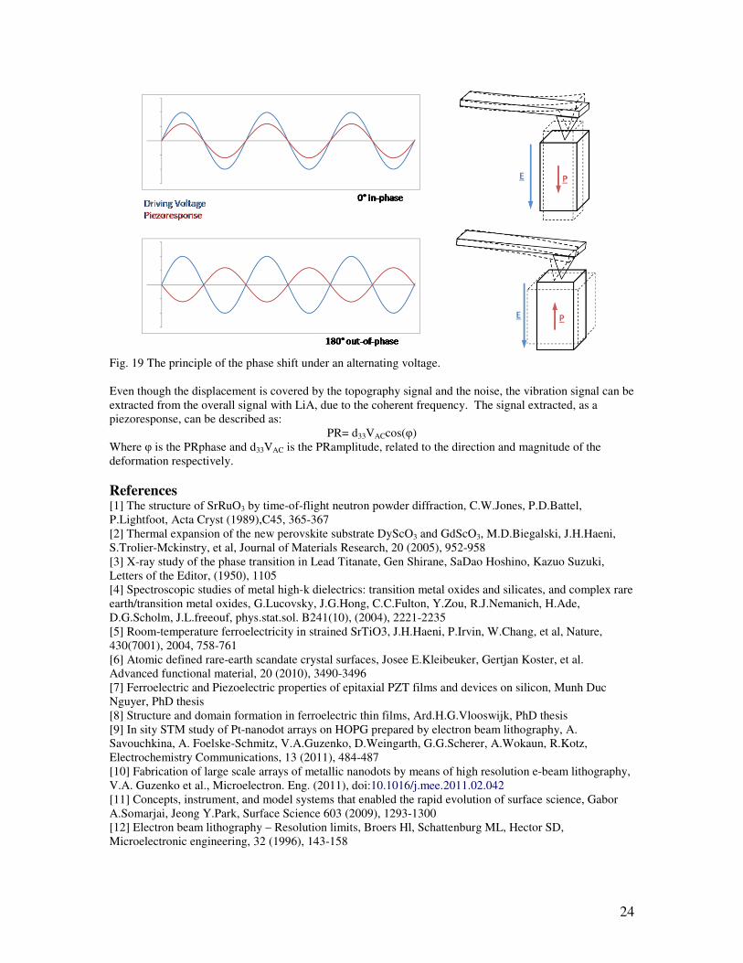
24
Fig. 19 The principle of the phase shift under an alternating voltage. Even though the displacement is covered by the topography signal and the noise, the vibration signal can be extracted from the overall signal with LiA, due to the coherent frequency. The signal extracted, as a piezoresponse, can be described as:
PR= d33VACcos(φ) Where φ is the PRphase and d33VAC is the PRamplitude, related to the direction and magnitude of the deformation respectively. References [1] The structure of SrRuO3 by time-of-flight neutron powder diffraction, C.W.Jones, P.D.Battel, P.Lightfoot, Acta Cryst (1989),C45, 365-367 [2] Thermal expansion of the new perovskite substrate DyScO3 and GdScO3, M.D.Biegalski, J.H.Haeni, S.Trolier-Mckinstry, et al, Journal of Materials Research, 20 (2005), 952-958 [3] X-ray study of the phase transition in Lead Titanate, Gen Shirane, SaDao Hoshino, Kazuo Suzuki, Letters of the Editor, (1950), 1105 [4] Spectroscopic studies of metal high-k dielectrics: transition metal oxides and silicates, and complex rare earth/transition metal oxides, G.Lucovsky, J.G.Hong, C.C.Fulton, Y.Zou, R.J.Nemanich, H.Ade, D.G.Scholm, J.L.freeouf, phys.stat.sol. B241(10), (2004), 2221-2235 [5] Room-temperature ferroelectricity in strained SrTiO3, J.H.Haeni, P.Irvin, W.Chang, et al, Nature, 430(7001), 2004, 758-761 [6] Atomic defined rare-earth scandate crystal surfaces, Josee E.Kleibeuker, Gertjan Koster, et al. Advanced functional material, 20 (2010), 3490-3496 [7] Ferroelectric and Piezoelectric properties of epitaxial PZT films and devices on silicon, Munh Duc Nguyer, PhD thesis [8] Structure and domain formation in ferroelectric thin films, Ard.H.G.Vlooswijk, PhD thesis [9] In sity STM study of Pt-nanodot arrays on HOPG prepared by electron beam lithography, A. Savouchkina, A. Foelske-Schmitz, V.A.Guzenko, D.Weingarth, G.G.Scherer, A.Wokaun, R.Kotz, Electrochemistry Communications, 13 (2011), 484-487 [10] Fabrication of large scale arrays of metallic nanodots by means of high resolution e-beam lithography, V.A. Guzenko et al., Microelectron. Eng. (2011), doi:10.1016/j.mee.2011.02.042 [11] Concepts, instrument, and model systems that enabled the rapid evolution of surface science, Gabor A.Somarjai, Jeong Y.Park, Surface Science 603 (2009), 1293-1300 [12] Electron beam lithography – Resolution limits, Broers Hl, Schattenburg ML, Hector SD, Microelectronic engineering, 32 (1996), 143-158
25
[13] Secondary electron generation in electron-beam irradiated solids: resolution limits to nanolithography, Kyu Won Lee, S.M.Yoon, S.C.Lee, W.Lee, I.-M.Kim and Cheol Eui Lee, Journal of the Korean Physical Society, 55 (2009), 1720-1723 [14] Electron optical column for a multicolumn, multibeam direct-write electron beam lithography, E.Yin, A.D.Brodie, F.C.Tsai, G.X.Guo, N.W.Parker, J.Vac.Sci, 18 (2000), 3126 [15] Electron beam lithography with the scanning tunneling microscope, Christie R.K.Marrian, Elizabeth A. Dobisz, J.Vac.Sci, 10B (1992), 2877-2881 [16] Field emission characteristics of the scanning tunneling microscope for nanolithography, T.M.Mayer, D.P.Adams, B.M.Marder, J.Vac.Sci, 14B (1996), 2438-2444 [17] The local piezoelectric activity of thin polymer films absorbed by scanning tunneling microscopy. H.Birk, J.Glatz-Reichenbach, Li Jie, E.Schreck, k.Dransfeld, J.Vac.Sci.Technol.B 9(2), 1991, 1162-1165 [18] Investigation of local piezoelectric properties of thin copolymer films. Perter Guthner, Joachim Glatz-Reichenbach, Klaus Dransfeld, J.Appl.Phys. 69(11) (1991) 7895-7897 [19] Local poling of ferroelectric polymers by scanning force microscopy. P.Guthner, K.Dransfeld, Appl.Phys.Lett, 61(9) (1992), 1137-1139 [20] Modification and detection of domains on ferroelectric PZT films by scanning force microscopy, K.Franke, J.Besold, W.Haessller, C.Seegebarth, Surface Science Letters, 302 (1994), 283-288 [21] Scanning force microscopy for the study of domain structure in ferroelectric thin films, A.Gruverman, O.Auciello, H.Tokumoto, J.Vac.Sci.Technol. B 14(2) (1996), 602-605 [22] Nanoscale investigation of fatigue effects in Pb(Zr,Ti)O3 films, A. Gruverman, O.Auciello, H.Tokumoto, Appl.Phys.Lett, 69(21) (1996), 3191-3193 [23] Scanning force microscopy of domain structrure in ferroelectric thin films: imaging andcontrol, A.Gruverman, O.Auciello, R.Ramesh, H.Tokumoto, Nanotechnology 8 (1997), A38-A43 [24] Scanning force microscopy study of domain structrure in Pb(ZrxTi1-x)O3 thin films and Pt/PZT/Pt and RuO2/PZT/RuO2 capacitors, O.Auciello, A.Gruverman, H.Tokumoto, Integrated ferroelectrics, 15 (1997), 107-114 [25] Nondestructive imaging and characterization of ferroelectric domains in periodically poled crystals, L.M.Eng, H.J.Guntherodt, G.Roseman, A.Skliar, M.Oron, M.Katz, D.Eger, J.Appl.Phys. 83 (1998), 5973 [26] Nanoscale reconstruction of surface crystallography from three dimensional polarization distribution in ferroelectric barium-titanate ceramics, L.M.Eng, H.J.Guntherodot, G.A.scheider, U.Kopke, j.M.Saldana, Appl.Phys.Lett, 74 (1999),233
26
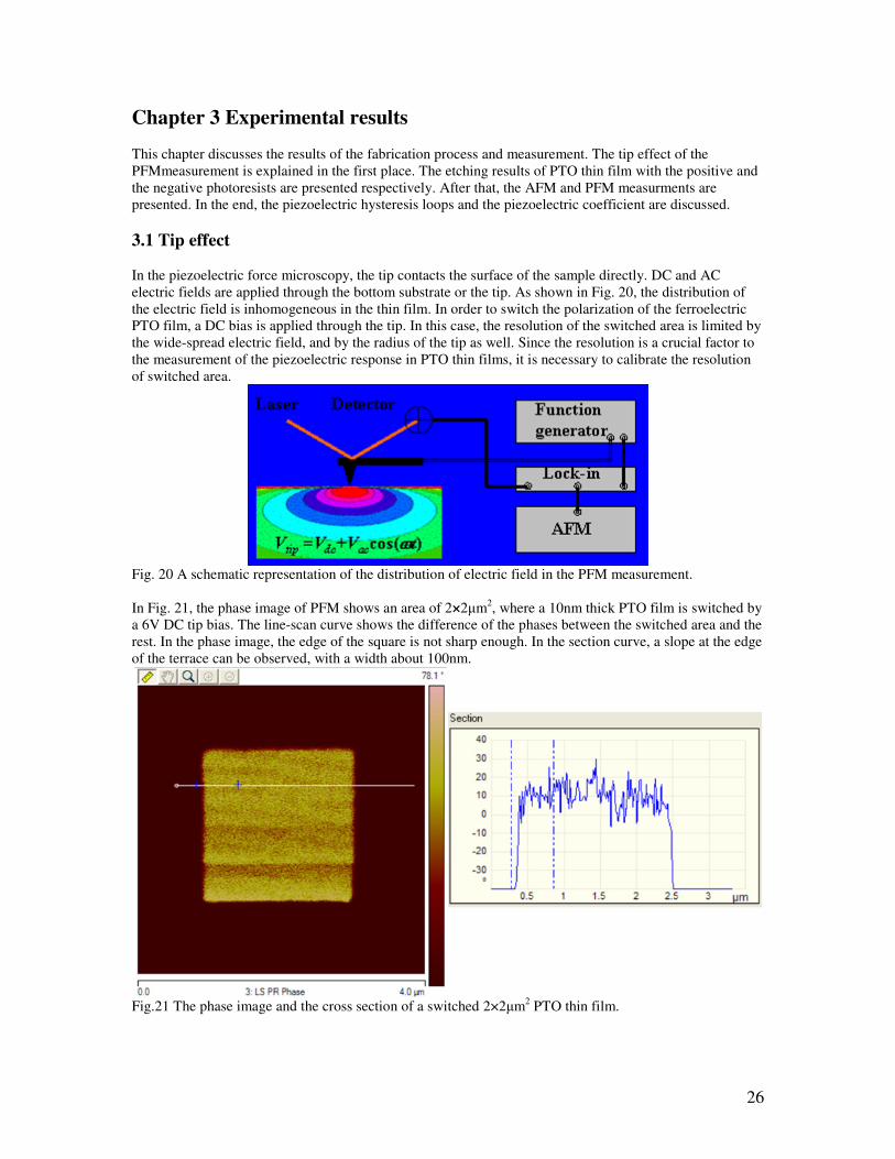
Chapter 3 Experimental results This chapter discusses the results of the fabrication process and measurement. The tip effect of the PFMmeasurement is explained in the first place. The etching results of PTO thin film with the positive and the negative photoresists are presented respectively. After that, the AFM and PFM measurments are presented. In the end, the piezoelectric hysteresis loops and the piezoelectric coefficient are discussed. 3.1 Tip effect In the piezoelectric force microscopy, the tip contacts the surface of the sample directly. DC and AC electric fields are applied through the bottom substrate or the tip. As shown in Fig. 20, the distribution of the electric field is inhomogeneous in the thin film. In order to switch the polarization of the ferroelectric PTO film, a DC bias is applied through the tip. In this case, the resolution of the switched area is limited by the wide-spread electric field, and by the radius of the tip as well. Since the resolution is a crucial factor to the measurement of the piezoelectric response in PTO thin films, it is necessary to calibrate the resolution of switched area.
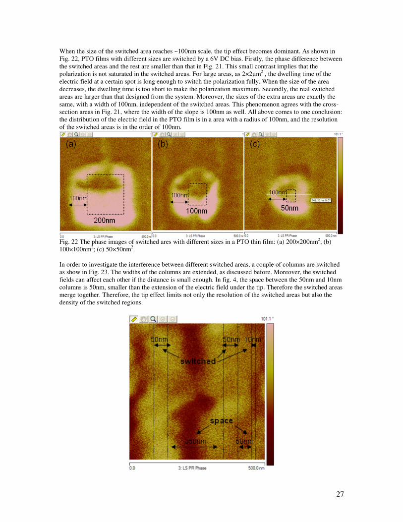
Fig. 20 A schematic representation of the distribution of electric field in the PFM measurement. In Fig. 21, the phase image of PFM shows an area of 2×2µm2, where a 10nm thick PTO film is switched by a 6V DC tip bias. The line-scan curve shows the difference of the phases between the switched area and the rest. In the phase image, the edge of the square is not sharp enough. In the section curve, a slope at the edge of the terrace can be observed, with a width about 100nm.
Fig.21 The phase image and the cross section of a switched 2×2µm2 PTO thin film.
27
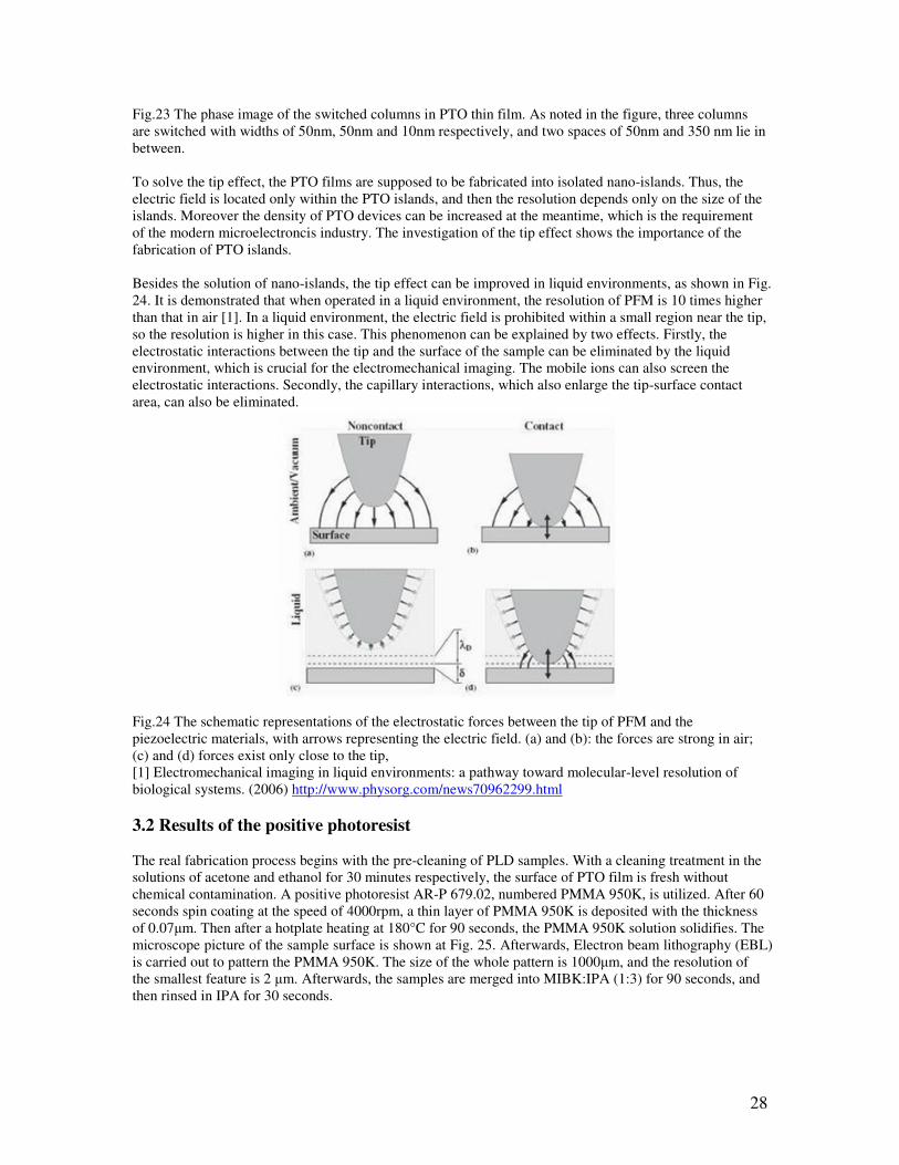
When the size of the switched area reaches ~100nm scale, the tip effect becomes dominant. As shown in Fig. 22, PTO films with different sizes are switched by a 6V DC bias. Firstly, the phase difference between the switched areas and the rest are smaller than that in Fig. 21. This small contrast implies that the polarization is not saturated in the switched areas. For large areas, as 2×2µm2 , the dwelling time of the electric field at a certain spot is long enough to switch the polarization fully. When the size of the area decreases, the dwelling time is too short to make the polarization maximum. Secondly, the real switched areas are larger than that designed from the system. Moreover, the sizes of the extra areas are exactly the same, with a width of 100nm, independent of the switched areas. This phenomenon agrees with the cross-section areas in Fig. 21, where the width of the slope is 100nm as well. All above comes to one conclusion: the distribution of the electric field in the PTO film is in a area with a radius of 100nm, and the resolution of the switched areas is in the order of 100nm.
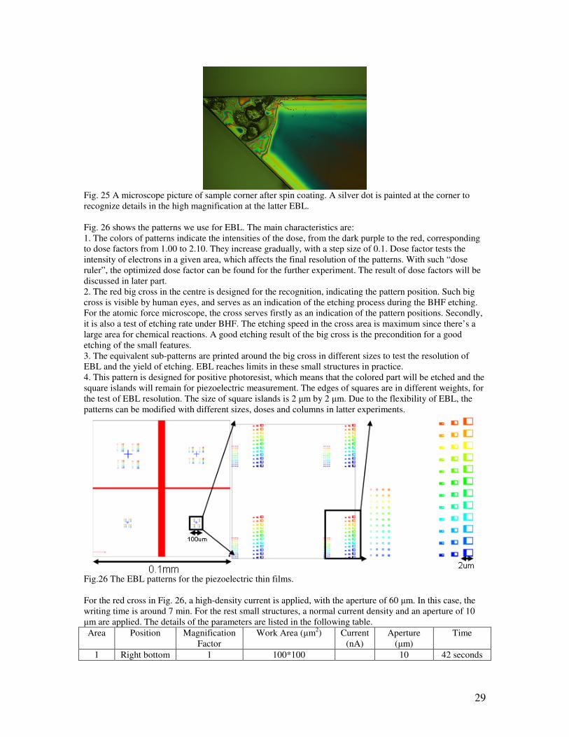
Fig. 22 The phase images of switched ares with different sizes in a PTO thin film: (a) 200×200nm2; (b) 100×100nm2; (c) 50×50nm2. In order to investigate the interference between different switched areas, a couple of columns are switched as show in Fig. 23. The widths of the columns are extended, as discussed before. Moreover, the switched fields can affect each other if the distance is small enough. In fig. 4, the space between the 50nm and 10nm columns is 50nm, smaller than the extension of the electric field under the tip. Therefore the switched areas merge together. Therefore, the tip effect limits not only the resolution of the switched areas but also the density of the switched regions.
28
Fig.23 The phase image of the switched columns in PTO thin film. As noted in the figure, three columns are switched with widths of 50nm, 50nm and 10nm respectively, and two spaces of 50nm and 350 nm lie in between. To solve the tip effect, the PTO films are supposed to be fabricated into isolated nano-islands. Thus, the electric field is located only within the PTO islands, and then the resolution depends only on the size of the islands. Moreover the density of PTO devices can be increased at the meantime, which is the requirement of the modern microelectroncis industry. The investigation of the tip effect shows the importance of the fabrication of PTO islands. Besides the solution of nano-islands, the tip effect can be improved in liquid environments, as shown in Fig. 24. It is demonstrated that when operated in a liquid environment, the resolution of PFM is 10 times higher than that in air [1]. In a liquid environment, the electric field is prohibited within a small region near the tip, so the resolution is higher in this case. This phenomenon can be explained by two effects. Firstly, the electrostatic interactions between the tip and the surface of the sample can be eliminated by the liquid environment, which is crucial for the electromechanical imaging. The mobile ions can also screen the electrostatic interactions. Secondly, the capillary interactions, which also enlarge the tip-surface contact area, can also be eliminated.
Fig.24 The schematic representations of the electrostatic forces between the tip of PFM and the piezoelectric materials, with arrows representing the electric field. (a) and (b): the forces are strong in air; (c) and (d) forces exist only close to the tip, [1] Electromechanical imaging in liquid environments: a pathway toward molecular-level resolution of biological systems. (2006) http://www.physorg.com/news70962299.html 3.2 Results of the positive photoresist The real fabrication process begins with the pre-cleaning of PLD samples. With a cleaning treatment in the solutions of acetone and ethanol for 30 minutes respectively, the surface of PTO film is fresh without chemical contamination. A positive photoresist AR-P 679.02, numbered PMMA 950K, is utilized. After 60 seconds spin coating at the speed of 4000rpm, a thin layer of PMMA 950K is deposited with the thickness of 0.07µm. Then after a hotplate heating at 180°C for 90 seconds, the PMMA 950K solution solidifies. The microscope picture of the sample surface is shown at Fig. 25. Afterwards, Electron beam lithography (EBL) is carried out to pattern the PMMA 950K. The size of the whole pattern is 1000µm, and the resolution of the smallest feature is 2 µm. Afterwards, the samples are merged into MIBK:IPA (1:3) for 90 seconds, and then rinsed in IPA for 30 seconds.
29
Fig. 25 A microscope picture of sample corner after spin coating. A silver dot is painted at the corner to recognize details in the high magnification at the latter EBL. Fig. 26 shows the patterns we use for EBL. The main characteristics are: 1. The colors of patterns indicate the intensities of the dose, from the dark purple to the red, corresponding to dose factors from 1.00 to 2.10. They increase gradually, with a step size of 0.1. Dose factor tests the intensity of electrons in a given area, which affects the final resolution of the patterns. With such “dose ruler”, the optimized dose factor can be found for the further experiment. The result of dose factors will be discussed in later part. 2. The red big cross in the centre is designed for the recognition, indicating the pattern position. Such big cross is visible by human eyes, and serves as an indication of the etching process during the BHF etching. For the atomic force microscope, the cross serves firstly as an indication of the pattern positions. Secondly, it is also a test of etching rate under BHF. The etching speed in the cross area is maximum since there’s a large area for chemical reactions. A good etching result of the big cross is the precondition for a good etching of the small features. 3. The equivalent sub-patterns are printed around the big cross in different sizes to test the resolution of EBL and the yield of etching. EBL reaches limits in these small structures in practice. 4. This pattern is designed for positive photoresist, which means that the colored part will be etched and the square islands will remain for piezoelectric measurement. The edges of squares are in different weights, for the test of EBL resolution. The size of square islands is 2 µm by 2 µm. Due to the flexibility of EBL, the patterns can be modified with different sizes, doses and columns in latter experiments.
Fig.26 The EBL patterns for the piezoelectric thin films. For the red cross in Fig. 26, a high-density current is applied, with the aperture of 60 µm. In this case, the writing time is around 7 min. For the rest small structures, a normal current density and an aperture of 10 µm are applied. The details of the parameters are listed in the following table. Area Position Magnification
Factor Work Area (µm2) Current
(nA) Aperture
(µm) Time
1 Right bottom 1 100*100 10 42 seconds
30
2 Left Bottom 1 100×100 10 42 seconds 3 Right top 2 200×200 10 1.5 mins 4 Left top 3 200×200
0.033
10 3 mins Cross Centre - 1000×1000 3.10 60 7mins
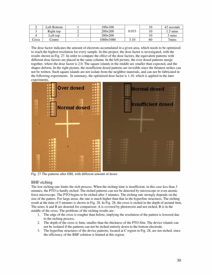
The dose factor indicates the amount of electrons accumulated in a given area, which needs to be optimized to reach the highest resolution for every sample. In this project, the dose factor is investigated, with the results shown in Fig. 27. In order to compare the effect of the dose factors, the equivalent patterns with different dose factors are placed in the same column. In the left picture, the over dosed patterns merge together, where the dose factor is 2.0. The square islands in the middle are smaller than expected, and the shapes deform. In the right picture, the insufficient dosed patterns are invisible since the thinnest strikes can not be written. Such square islands are not isolate from the neighbor materials, and can not be fabricated in the following experiments. In summary, the optimized dose factor is 1.10, which is applied in the later experiments.
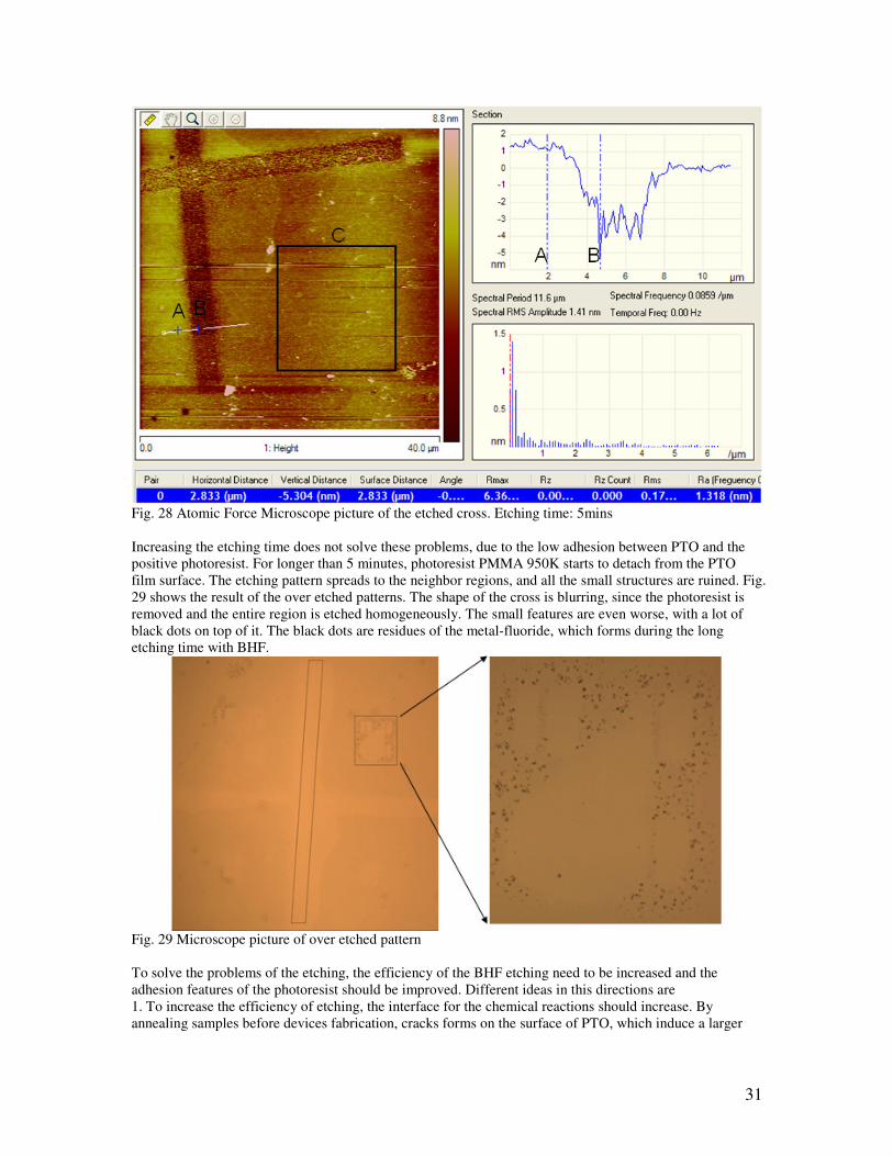
Fig. 27 The patterns after EBL with different amount of doses BHF etching The low etching rate limits the etch process. When the etching time is insufficient, in this case less than 3 minutes, the PTO is hardly etched. The etched patterns can not be detected by microscope or even atomic force microscope. The PTO begins to be etched after 3 minutes. The etching rate strongly depends on the size of the patters. For large areas, the rate is much higher than that in the hyperfine structures. The etching result at the time of 5 minutes is shown in Fig. 28. In Fig. 28, the cross is etched in the depth of around 4nm. The notes A and B are denoted for comparison: A is covered by photoresist and not etched, B is in the middle of the cross. The problems of the etching results are:
1. The edge of the cross is rougher than before, implying the resolution of the pattern is lowered due to the etching process.
2. The depth of the cross is 4nm, smaller than the thickness of the PTO film. The device islands can not be isolated if the patterns can not be etched entirely down to the bottom electrode.
3. The hyperfine structures of the device patterns, located at C region in Fig. 28, are not etched, since the efficiency of the BHF solution is limited at this region.
31
Fig. 28 Atomic Force Microscope picture of the etched cross. Etching time: 5mins Increasing the etching time does not solve these problems, due to the low adhesion between PTO and the positive photoresist. For longer than 5 minutes, photoresist PMMA 950K starts to detach from the PTO film surface. The etching pattern spreads to the neighbor regions, and all the small structures are ruined. Fig. 29 shows the result of the over etched patterns. The shape of the cross is blurring, since the photoresist is removed and the entire region is etched homogeneously. The small features are even worse, with a lot of black dots on top of it. The black dots are residues of the metal-fluoride, which forms during the long etching time with BHF.
Fig. 29 Microscope picture of over etched pattern To solve the problems of the etching, the efficiency of the BHF etching need to be increased and the adhesion features of the photoresist should be improved. Different ideas in this directions are 1. To increase the efficiency of etching, the interface for the chemical reactions should increase. By annealing samples before devices fabrication, cracks forms on the surface of PTO, which induce a larger
32
interface. However, in this case, the properties of devices islands in the order of hundreds nanometers will decay because of the coherent length. 2. To avoid the adhesion problem, a negative photoresist can replace the PMMA 950K. The adhesion property of negative photoresists is higher than PMMA, while the resolution is lower, 100nm compared with 10nm of PMMA 950K. For negative photoresists, the etching areas are larger, which implies a high etching rate. 3. Other etching methods can be applied, for example reactive ion etching, focused ion beam etching. Other devices fabrication techniques are available as well. 3.3 Results of the negative photoresist The negative photoresist applied in this experiment is ma-N2401, one of the members in the ma-N2400 series. ma-N 2400 is a negative tone photoresist series designed for the use in micro- and nanoelectroncis. The physical properties of the resists are listed below: Resist ma-N 2401 ma-N 2403 ma-N 2405 ma-N 2410 Film thickness [µm] 0.1±0.02 0.3±0.02 0.5±0.02 1.0±0.02 Dynamic Viscosity [mPa s] 5±1 7±1 8±1 12±1 Density [g cm3] 1.005±0.002 1.025±0.002 1.036±0.002 1.056±0.002
Fig. 30 The fabrication process of the PTO islands with the negative photoresist. The fabrication process of the negative photoresist, as shown in Fig. 30, starts with the cleaning treatment of the PTO thin film. The PLD sample is cleaned by acetone and then ethanol for 30 minutes respectively in the ultrasonic bath at the room temperature. After that, the surface of the sample is fresh and free of impurities. Dehydration, ozone plasma cleaning or baking are not applied since the adhesion of ma-N 2401 to the PTO surface is good enough. The photoresist film with 100nm thickness forms after the spin coating at 3000 RPM for 30 seconds. After a baking on the hotplate at 90°C for 60 seconds, the solvent evaporates and the photoresist solidifies. The surface image of the sample with the photoresist above is shown in Fig. 31. After that, the electron beam lithography (EBL) is applied to draw the patterns on the resist, with the smallest feature at 200nm. The details of EBL process will be explained later. After that, the sample is

33
merged into a developer named ma-D 532 for 4 minutes at the room temperature, and then rinsed in deionized water for 5 minutes.
Fig. 31 The microscope image of a sample corner after the spin coating. The colors on the edge imply that the thickness of the photoresist decreases from the centre to the edge.
Fig. 32 The EBL patterns for the piezoelectric thin film islands with the negative photoresist. The ELB patterns of the negative photoresist are shown in Fig. 32. 1. The color of the pattern indicates the intensity of the dose of electrons. In this pattern, from dark blue to red, the dose increases from 200µC/cm2 to 500µC/cm2 gradually. The dose factor affects the resolution of the photoresist. The result of the photoresist with different doses will be discussed latter. 2. The small features are designed in different sizes. As shown in Fig. 32, the sizes of the square islands are 5µm, 3µm, 1µm, 0.5µm and 0.2µm respectively. Since the resolution of the ma-N2400 resist is around 100nm, no smaller features can be drawn on this type of photoresist. The big cross on the left picture is in the size of 1000µm×1000µm, which serves as an indication of the position of the pattern. Such big cross can be recognized by the optical microscope of the AFM and human eyes. The small bars on the big cross are the signs of the small squares. In the AFM and PFM measurements, the small features can be found from these bars. 3. The small features are copied four times and locate in different areas. In this case, the yield of islands can be increased. The parameters of the EBL patterns are listed below.
Area Work Area (µm× µm)
Current (nA)
Work distance (mm)
Acceleration Voltage (kV)
Aperture (µm)
Time
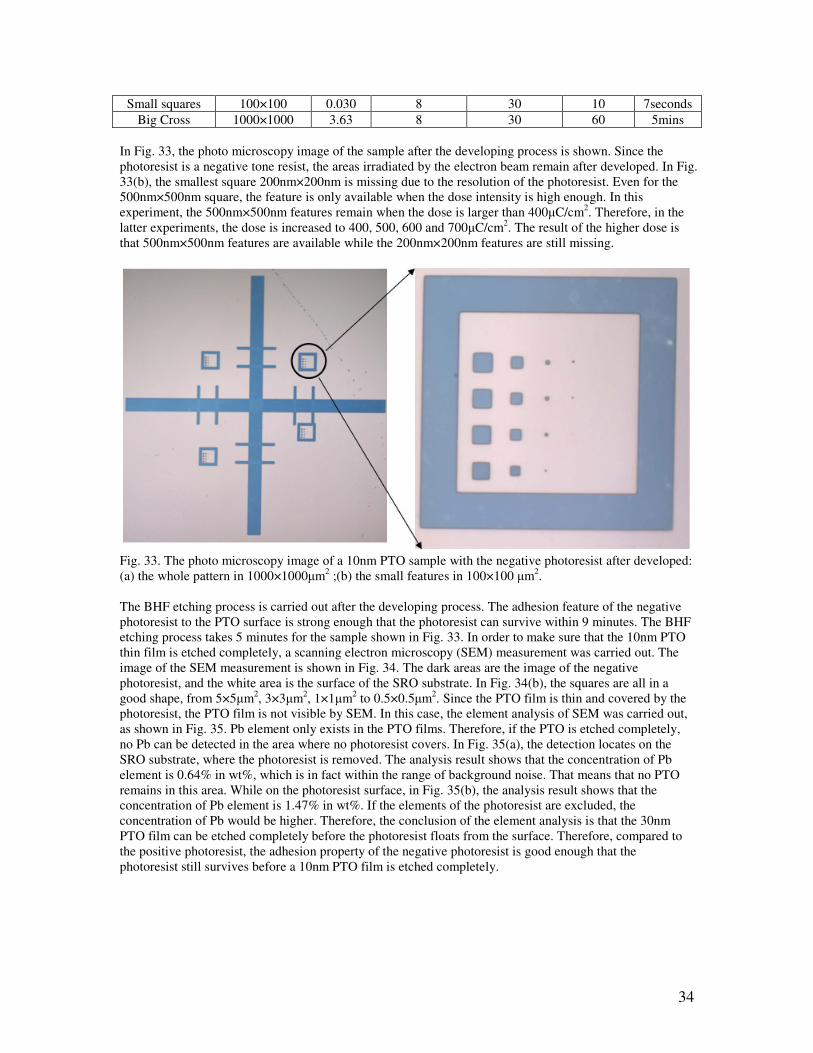
34
Small squares 100×100 0.030 8 30 10 7seconds Big Cross 1000×1000 3.63 8 30 60 5mins
In Fig. 33, the photo microscopy image of the sample after the developing process is shown. Since the photoresist is a negative tone resist, the areas irradiated by the electron beam remain after developed. In Fig. 33(b), the smallest square 200nm×200nm is missing due to the resolution of the photoresist. Even for the 500nm×500nm square, the feature is only available when the dose intensity is high enough. In this experiment, the 500nm×500nm features remain when the dose is larger than 400µC/cm2. Therefore, in the latter experiments, the dose is increased to 400, 500, 600 and 700µC/cm2. The result of the higher dose is that 500nm×500nm features are available while the 200nm×200nm features are still missing.
Fig. 33. The photo microscopy image of a 10nm PTO sample with the negative photoresist after developed: (a) the whole pattern in 1000×1000µm2 ;(b) the small features in 100×100 µm2. The BHF etching process is carried out after the developing process. The adhesion feature of the negative photoresist to the PTO surface is strong enough that the photoresist can survive within 9 minutes. The BHF etching process takes 5 minutes for the sample shown in Fig. 33. In order to make sure that the 10nm PTO thin film is etched completely, a scanning electron microscopy (SEM) measurement was carried out. The image of the SEM measurement is shown in Fig. 34. The dark areas are the image of the negative photoresist, and the white area is the surface of the SRO substrate. In Fig. 34(b), the squares are all in a good shape, from 5×5µm2, 3×3µm2, 1×1µm2 to 0.5×0.5µm2. Since the PTO film is thin and covered by the photoresist, the PTO film is not visible by SEM. In this case, the element analysis of SEM was carried out, as shown in Fig. 35. Pb element only exists in the PTO films. Therefore, if the PTO is etched completely, no Pb can be detected in the area where no photoresist covers. In Fig. 35(a), the detection locates on the SRO substrate, where the photoresist is removed. The analysis result shows that the concentration of Pb element is 0.64% in wt%, which is in fact within the range of background noise. That means that no PTO remains in this area. While on the photoresist surface, in Fig. 35(b), the analysis result shows that the concentration of Pb element is 1.47% in wt%. If the elements of the photoresist are excluded, the concentration of Pb would be higher. Therefore, the conclusion of the element analysis is that the 30nm PTO film can be etched completely before the photoresist floats from the surface. Therefore, compared to the positive photoresist, the adhesion property of the negative photoresist is good enough that the photoresist still survives before a 10nm PTO film is etched completely.
35
Fig. 34 The SEM image of PTO sample after etching. (a) the top view of the pattern; (b) & (c) the size view of the small features; (d) the schematic structure of the PTO sample.
36
Fig. 35 The element analysis of SEM: (a) in the area of the SRO substrate, where no photoresist or PTO exist, Pb at wt% is 0.64%; (b) in the area of the photoresist, where PTO is underneath, Pb at wt% is 1.47%. The photoresist is removed by acetone after the SEM measurement. The pattern of the PTO islands can be observed by the microscope directly, as show in Fig. 36. The edges of the square are in a good shape. The 5×5µm2 and the 3×3µm2 islands are visible, while the 1×1µm2 and the 0.5×0.5µm2 are not visible from the microscope. The contrast is a bit low since the difference of the heights between the PTO islands and SRO electrode is only 30nm.
37
Fig. 36 The microscope image of the PTO islands. In the Atomic Force Microscopy (AFM) measurement, the PTO islands are visible and clear. The bright part in Fig. 37(a) is the region of PTO islands. In Fig. 37(b), the line scan across the image shows the height of the island. After the 9 minutes of the BHF etching, the 30 nm PTO film is almost etched except the regions covered by the photoresist. Then Fig. 38 shows the topography and the cross section of the 3×3µm2 PTO island in the same way. Fig. 39 shows both the 1×1µm2 and the 0.5×0.5µm2 islands. The edges of the islands are rough in this case, which means that the resolution of the etching process limits the sizes of islands.
Fig. 37 An AFM image of a 5×5µm2 PTO island. (a) the topography of the island; (b) the line scan along the A-B line. The two spots A and B in (a) correspond to A and B spots in (b), respectively.
38
Fig. 38 An AFM image of a 3×3µm2 PTO island. (a) the topography of the island; (b) the cross section of the A-B line. The two spots A and B in (a) correspond to A and B spots in (b), respectively.
Fig. 39 An AFM image of 1×1µm2 and 0.5×0.5µm2 PTO islands. 3.4 Ferroelectric properties of the PTO islands
39
After the measurement of the topography, Piezoelectric Force Microscopy (PFM) was utilized to measure the piezoelectric and ferroelectric properties of PTO islands. As shown in Fig. 40, the PFM measurement is in the contact mode. Both AC and DC bias are applied to the thin film. The tip contacts the PTO surface and a DC bias is applied through the tip. The polarization of the ferroelectric PTO film is switched by this DC bias. The sample is placed on the metal substrate, through which an AC bias is applied from the bottom. The AC bias serves for the Lock-in amplifier technique, which can extract the signal of the deformation with the same frequency from the background noise. The tip bias (DC bias) is 3V, which is sufficient to switch the polarization. As for the AC bias applied from the bottom, the amplitude is 5000mV and the frequency is 50kHz.
Fig. 40 A schematic picture of the PFM setup.
Fig. 41 A switched 2×2µm2 region in the centre of the 5×5µm2 PTO island: (a) the phase image of the PFM measurement; (b) the schematic representation of the ferroelectric polarization in a PTO island; (c) the cross section of the phase image. A 2×2µm2 square region in the centre of a 5×5µm2 PTO island is switched by PFM, as shown in Fig. 41. The phase image describes the phase shift between the applied AC applied electric field and the deformation of the sample surface. Ideally, the phase difference is zero when the polarization is parallel to the electric field, and 180° when the polarization is opposite to the field. In Fig. 41(a), the 2×2µm2 square
40
region is switched with a nice shape of the edge. In this area, the direction of the spontaneous polarization is down, while in the rest area, the polarizations are either in plane or out to place randomly. In Fig. 41(c), the cross section of the phase image shows that the phase difference between the switched region and the rest part is around 90°, with a good agreement with the previous explanation. Similar results were observed in the 3×3µm2, 1×1µm2 islands. This result implies that the PTO crystal still stays in the ferroelectric phase when the dimensions decrease to the scale of 1µm. 3.5 Piezoelectric hysteresis loops The piezoelectric hysteresis loop is measured while the bis voltage is ramped in between two values. Similar to PFM, a DC bias is applied from the tip to switch the polarization, and an AC bias is applied from the bottom electrode to get rid of the noise by the Lock-in Amplifier. The tip is located at one certain place to measure the piezoelectric response instead of scanning a region. The DC bias starts from -3V to 3V, and then traces back to -3V. Two hysteresis loops are obtained. The phase of the piezoelectric response (PRphase) shows when the polarization is switched and the phase difference between the two polarization states. The amplitude of the piezoelectric response (PRamplitude) shows the out-of-plane deformation of the PTO islands as a function of the DC bias.
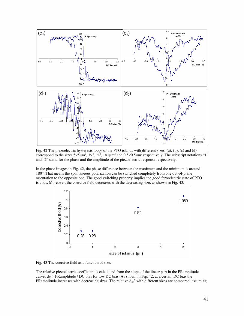
41
Fig. 42 The piezoelectric hysteresis loops of the PTO islands with different sizes. (a), (b), (c) and (d) correspond to the sizes 5×5µm2, 3×3µm2, 1×1µm2 and 0.5×0.5µm2 respectively. The subscript notations “1” and “2” stand for the phase and the amplitude of the piezoelectric response respectively. In the phase images in Fig. 42, the phase difference between the maximum and the minimum is around 180°. That means the spontaneous polarization can be switched completely from one out-of-plane orientation to the opposite one. The good switching property implies the good ferroelectric state of PTO islands. Moreover, the coercive field decreases with the decreasing size, as shown in Fig. 43.
Fig. 43 The coercive field as a function of size. The relative piezoelectric coefficient is calculated from the slope of the linear part in the PRamplitude curve: d33’=PRamplitude / DC bias for low DC bias. As shown in Fig. 42, at a certain DC bias the PRamplitude increases with decreasing sizes. The relative d33’ with different sizes are compared, assuming
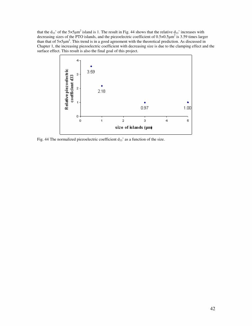
42
that the d33’ of the 5×5µm2 island is 1. The result in Fig. 44 shows that the relative d33’ increases with decreasing sizes of the PTO islands, and the piezoelectric coefficient of 0.5×0.5µm2 is 3.59 times larger than that of 5×5µm2. This trend is in a good agreement with the theoretical prediction. As discussed in Chapter 1, the increasing piezoelectric coefficient with decreasing size is due to the clamping effect and the surface effect. This result is also the final goal of this project.
Fig. 44 The normalized piezoelectric coefficient d33’ as a function of the size.
43
Conclusion This project integrates the size effects of the piezoelectric response in ferroelectric thin films of PbTiO3 (PTO), from the fabrication of the PTO nano-islands to the PFM measurement of the piezoelectric hysteresis loop. A couple of conclusions can be made from the experimental results: Tip effect: the lateral distribution of the electric field applied from a PFM tip extends across radius of about 100nm. This effect can be attenuated when the PTO films are isolated into islands, as done in this project. Positive photoresist: the adhesion property of the positive photoresist AR-P 679.02 is not strong enough, so that the photoresist floats before a 10nm PTO film is completely etched by buffered-HF. To improve the etching process, the etching speed should be increased by utilizing BHF with a higher acid concentration, or the adhesion property should be improved by optimizing the spin-coat and baking process. Negative photoresist: the adhesion property of the negative photoresist ma-N 2401 is good enough to cover the PTO film during the etching process. A 30nm PTO film can be completely etched by the 12% BHF in 9 minutes. The smallest PTO island in this process is 0.5×0.5µm2. Switching property: The spontaneous polarization of the PTO islands can be switched from one out-of-plane orientation to the opposite orientation under a 3V DC bias. The switchable polarization implies that the PTO islands are still in good ferroelectric state even, when the lateral size goes down to the order of 1µm. Piezoelectric hysteresis loop: the piezoelectric response can be measured by ramping the DC field in between tow values from -3V to 3V and back to -3V, in order to write a hysteresis loop. The phase image shows that the polarization can be switched at a coercive electric field that decreases with decreasing island sizes. The amplitude image shows that the deformations of the PTO islands increase with decreasing sizes. Thus, the piezoelectric coefficient increases when the sizes of the PTO islands get smaller. The piezoelectric coefficient of the 0.5×0.5µm2 PTO island is 3.59 times larger than that of 5×5µm2 one. This result is in a good agreement with the theoretical prediction. Therefore, the size effect of the piezoelectric coefficient is proven in this project.

44
Improvement and future plan The size effect of the piezoelectric coefficient is supposed to be more significant when the size gets smaller. To achieve this goal, both the fabrication process and the measurement need to be optimized.
1. The edges of the PTO islands are not in a good shape, which would be a crucial restriction if the size of the islands goes down to ~100×100nm2. In this case, a BHF with a higher concentration can be utilized to reduce the etching time. The PTO thin film is etched vertically first and then laterally later. The shape of the PTO depends on the lateral etching. By reducing the etching time, PTO islands in good shapes can be maintained.
2. The resolution of the negative photoresist is around 100nm, while in this project the 0.2×0.2µm2 can not be written by EBL. In order to reach the minimum size 100×100nm2, the fabrication process needs to be optimized, including the spin coating, baking and the parameters of EBL.
3. A top electrode is necessary for the PTO devices. Firstly, the top electrode can protect the PTO film in the etching process. The flat PTO surface can be maintained in this case. Secondly, the distribution of the electric field in the PTO film would be homogenous if the top electrode exists. Before a top electrode is applied upon the PTO film, the etching technique for the top electrode has to be investigated. Reactive ion etching (RIE) can be applied for the etching of the top electrode.
4. In the measurement of the piezoelectric hysteresis loop, the background noise needs to be attenuated to get more accurate hysteresis loops. Moreover, in order to obtain the absolute value of the piezoelectric coefficient, the PRamplitude signal has to be calibrated and transformed into the deformation of PTO islands.

45
Acknowledgements I would like to thank Prof. Beatriz Noheda for offering me the chance to do my master project in the group “Solid-state material for electronics” (SSME) and for her supervising on this project. Porf. Beatriz Noheda gave me not only valuable advice on my master project, but also helpful guidance for my PhD application and proposal. Her friendly and kind-hearted attitude made me confident on my research. This project would have never started or finished without the guidance from my direct supervisor Oleksiy Nestrov. He provided the PLD samples for me and taught me how to operate AFM and EBL equipments. We fought against every challenge together during the whole process, and cooperated with each other quite well. I would like to acknowledge the Technician Johan.G.Holstein who granted Oleksiy and me to use the setups in the group of Nanodevices, and the PhD student Paul J.Zomer who taught Oleksiy and me how to use the EBL for many times. I would also like to thank our technician Jacob Baas, PhD students Saeedeh Farokhipoor and Jeroen A.Heuver, and my classmate Alim Solmaz, who helped every now and then for my research. I would also like to thank my previous supervisor Illias Katsouras, who taught me various fabrication skills of nanodevices and cleanroom experience. These techniques help a lot for my master project. I would like to deeply thank all the SSME group members. Our nice and funny lunch times on every workday will be my precious memory. Thank all of you for the advice you gave me during our FUN group meetings. The common welfare foundation Propondis is acknowledged for the finacial support during the two years of my studies in University of Groningen. Last but not least, I would like to express my gratitude to my caring and supportive family and friends.

46
Appendix: Operation commands of Electron beam lithography Raith 150
1. Open two computer screens. 2. Check whether the “EM server” is on the right screen and make sure no error messages on “EM
server” 3. Run the “Gun monitor” program to record parameters during the rest operations. 4. Open the “Column Interface” program and log in with your own account. 5. Open the “Aperture monitor” window for later use. 6. Click the “Vacuum” button on the right bottom corner and “vent” the chamber. 7. On the left screen, open the “E-line” and log in with your own account. 8. When the chamber is vented, fix the sample in the platform with gloves on hands. 9. “Pump” the chamber, and wait until the “vacuum” button is green. 10. Click the second traffic light on the left screen, and choose “load sample” 11. After the loading procedure is done, set some EBL parameters in the dialogue window: Gun
voltage 30kV, aperture 10 µm, and work distance 8 mm. Do not save this setting for the “E-line” program, and then set your sample same and save it.
12. In the “Stage Control” window, choose “Command” menu and type “25z” to activate the control. 13. Choose “FARADAY” command to locate the gun monitor to the hole of the platform. 14. On the right screen, set “Signal A” to “SE2”, which corresponds to the top view of the platform? 15. Choose the “magnification” option, locate the monitor to the centre of the hole, and then zoom in
to maximum. 16. Click “measure” button in the “Current” window of the right screen, to measure the current under
aperture 10 µm, and then record the value for further comparison. 17. In the “GDSII Database” window, open the file of your pattern. 18. Click “File” to create a new position list. 19. Drag the final pattern file from the “GDSII Database” to the position list. For each work area, a
corresponding list is required. 20. For one list, set the size of work area in “Microscope Control” window, options: 100 µm, 200 µm,
300 µm, 1000 µm 21. For each size of work area, choose the corresponding work area in “Microscope Control”, and the
current should be measured again for the record. 22. Click right bottom on one list and choose “properties”. In the window of “properties”, choose the
layer of your patterns, set the region of work area and check from the “centre position”. 23. In “Exposure parameter” option, for normal current, set the area step size to 0.0064 µm and the
Area dose should be 100 µC/cm2. Then calculate the dwell time (around 0.001336ms). In the line step, set the parameter to 0.0064 µm as well. Calculate the dwell time too.
24. For high current, set both area step size and line step to 0.090µm, and repeat the other steps in 23. The parameters are listed in the table below.
Aperture (µm) 10 60 (High current) Area step size (µm) 0.0064 0.0936 Area dwell time (ms) 0.001336 0.003248 Area dose (µC/cm2) 100 100 Line step size (µm) 0.0064 0.0936 Line dwell time (ms) 0.025049 0.004164 Line dose (µC/cm2) 100 100
25. Calculate the “Dwell Time” for each area to check whether the work area locates in proper place
and compare the time with the previous data. 26. Double click the work areas to check the positions 27. On the navigation window of the left screen, find a tiny structure on the test samples at the scale of
1 µm, focus the image to find the best resolution. 28. Click the middle button of the mouth on the “spot shoot” button, and then wait approximate 1
minute to burn a spot on test samples. 29. Click the middle button of the mouth 1 minute later, and then check the spot. If a spot is burnt on
the sample, go on the next steps, otherwise adjust the work distance and try again.
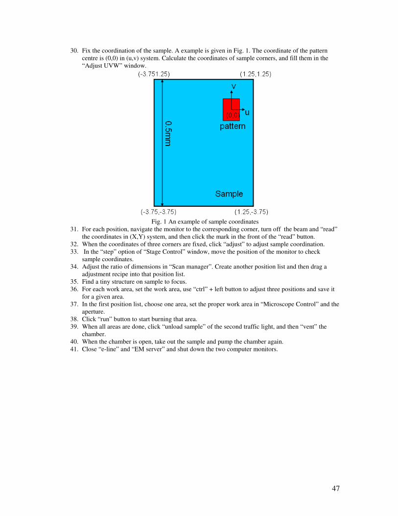
47
30. Fix the coordination of the sample. A example is given in Fig. 1. The coordinate of the pattern centre is (0,0) in (u,v) system. Calculate the coordinates of sample corners, and fill them in the “Adjust UVW” window.
Fig. 1 An example of sample coordinates
31. For each position, navigate the monitor to the corresponding corner, turn off the beam and “read” the coordinates in (X,Y) system, and then click the mark in the front of the “read” button.
32. When the coordinates of three corners are fixed, click “adjust” to adjust sample coordination. 33. In the “step” option of “Stage Control” window, move the position of the monitor to check
sample coordinates. 34. Adjust the ratio of dimensions in “Scan manager”. Create another position list and then drag a
adjustment recipe into that position list. 35. Find a tiny structure on sample to focus. 36. For each work area, set the work area, use “ctrl” + left button to adjust three positions and save it
for a given area. 37. In the first position list, choose one area, set the proper work area in “Microscope Control” and the
aperture. 38. Click “run” button to start burning that area. 39. When all areas are done, click “unload sample” of the second traffic light, and then “vent” the
chamber. 40. When the chamber is open, take out the sample and pump the chamber again. 41. Close “e-line” and “EM server” and shut down the two computer monitors.