pk2600 - phil pem
TRANSCRIPT
Users ManualRevision C
PK2600Integrated Control System
PK2600 Users ManualPart Number 019-0061
Revision C
Last revised on July 20, 2000 Printed in U.S.A.
Copyright© 1999 Z-World, Inc.
All rights reserved.
Z-World reserves the right to make changes and improvements to itsproducts without providing notice.
Trademarks Dynamic C
® is a registered trademark of Z-World, Inc.
Windows®
is a registered trademark of Microsoft Corporation
PLCBus
is a trademark of Z-World, Inc.
Hayes Smart Modem®
is a registered trademark of Hayes MicrocomputerProducts, Inc.
Notice to UsersWhen a system failure may cause serious consequences, protecting lifeand property against such consequences with a backup system or safetydevice is essential. The buyer agrees that protection against conse-quences resulting from system failure is the buyers responsibility.
This device is not approved for life-support or medical systems.
All Z-World products are 100 percent functionally tested. Additionaltesting may include visual quality control inspections or mechanicaldefects analyzer inspections. Specifications are based on characterizationof tested sample units rather than testing over temperature and voltage ofeach unit. Z-World may qualify components to operate within a range ofparameters that is different from the manufacturers recommended range.This strategy is believed to be more economical and effective. Additionaltesting or burn-in of an individual unit is available by special arrangement.
Company Address
Z-World, Inc.2900 Spafford StreetDavis, California 95616-6800USA
Telephone:Facsimile:Web Site:
E-Mail:
(530) 757-3737(530) 753-5141http://www.z [email protected]

Table of Contents s iiiPK2600
TABLE OF CONTENTS
About This Manual ix
Chapter 1: Overview 13Features ............................................................................................... 15
Options ............................................................................................ 16Flexibility and Customization ............................................................... 16Development and Evaluation Tools ..................................................... 18
Developers Kit ................................................................................ 18Software .......................................................................................... 18
Chapter 2: Getting Started 19Initial PK2600 Setup ............................................................................. 20
Parts Required ................................................................................. 20Setting Up the PK2600 .................................................................... 20
Connecting the PK2600 to a Host PC ................................................... 22Running Dynamic C ............................................................................. 24
Chapter 3: Hardware Features 25Operating Modes ................................................................................. 26
Changing the Operating Mode ........................................................ 27Using Run and Program Modes: Example ..................................... 27
Liquid Crystal Display (LCD) ............................................................... 28Contrast Adjustment ....................................................................... 28Coordinate Systems ........................................................................ 29
Digital Inputs/Outputs ......................................................................... 30Digital Group 1 ................................................................................ 30Digital Group 2 ................................................................................ 30
Analog Inputs ...................................................................................... 31Serial Channels ..................................................................................... 32PLCBus ................................................................................................ 33
Chapter 4: Hardware Configurations 35PK2600 Assembly ................................................................................ 36
Accessing the Controller Board ...................................................... 38Accessing the Display Board .......................................................... 40
iv s Table of Contents PK2600
Digital Inputs and Outputs .................................................................. 41External Connections ....................................................................... 41Digital Inputs ................................................................................... 42
Operating Modes and Configuration ............................................ 42Digital Outputs ................................................................................ 45
Operating Modes and Configuration ............................................ 45High-Voltage Drivers ..................................................................... 45Using Output Drivers .................................................................... 49TTL/CMOS Outputs ..................................................................... 50Pulse-Width Modulation (PWM) Configuration .......................... 51
Analog Inputs ...................................................................................... 52Operating Modes and Configuration .............................................. 52
Drift ............................................................................................... 59Low-Pass Filter ............................................................................. 59Excitation Resistors ....................................................................... 60
Using the Unconditioned Converter Channels ............................... 60Internal Test Voltages ...................................................................... 60Power-Down Mode ......................................................................... 61External Connections ....................................................................... 61
Serial Channels ..................................................................................... 62Operating Modes and Configuration .............................................. 63Configuring a Multidrop Network ................................................... 65
RS-485 Termination ....................................................................... 65External Connections ....................................................................... 65
PLCBus ................................................................................................ 68Liquid Crystal Display (LCD) ............................................................... 69
Contrast Adjustments ..................................................................... 69Background ..................................................................................... 69
Chapter 5: Subsystems 71Controller Board Subsystems .............................................................. 72
Microprocessor Core Module ......................................................... 72Display Board Subsystems .................................................................. 74
Computing Module ......................................................................... 74Power Regulation ............................................................................ 75Serial Communication ...................................................................... 76
691 Supervisor Chip ............................................................................. 77System Reset ................................................................................... 79
Z180 Serial Ports ................................................................................... 80Use of the Serial Ports ..................................................................... 82
Table of Contents s vPK2600
Asynchronous Serial Communication Interface ................................... 83ASCI Status Registers ..................................................................... 83
/DCD0 (Data Carrier Detect) .......................................................... 83TIE (Transmitter Interrupt Enable) ................................................ 83TDRE (Transmitter Data Register Empty) ..................................... 83CTS1E (CTS Enable, Channel 1) .................................................... 84RIE (Receiver Interrupt Enable) ..................................................... 84FE (Framing Error) ......................................................................... 84PE (Parity Error) ............................................................................. 84OVRN (Overrun Error) ................................................................... 84RDRF (Receiver Data Register Full) .............................................. 84
ASCI Control Register A ................................................................. 85MOD0MOD2 (Data Format Mode Bits) ...................................... 85MPBR/EFR (Multiprocessor Bit Receive/Error Flag Reset) .......... 85/RTS0 (Request to Send, Channel 0) ............................................. 85CKA1D (CKA1 Disable) ............................................................... 85TE (Transmitter Enable) ................................................................ 85RE (Receiver Enable) ..................................................................... 86MPE (Multiprocessor Enable) ....................................................... 86
ASCI Control Register B ................................................................. 86SS (Source/Speed Select) .............................................................. 86DR (Divide Ratio) .......................................................................... 87PEO (Parity Even/Odd) ................................................................. 87/CTS/PS (Clear to Send/Prescaler) ................................................ 87MP (Multiprocessor Mode) .......................................................... 87MPBT (Multiprocessor Bit Transmit) ........................................... 87
Chapter 6: Software Development 89Supplied Software ................................................................................ 90Digital I/O ............................................................................................. 91
Digital Inputs ................................................................................... 91How to Read the Input .................................................................... 91
Sample Program ............................................................................. 92Digital Outputs ................................................................................ 93
Sample Program ............................................................................. 94Pulse-Width Modulated (PWM) Outputs ....................................... 95
How to Use the PWM Feature ...................................................... 95PWM Software ............................................................................. 96Sample Program ............................................................................. 97
Analog Inputs ...................................................................................... 98Using the Analog Inputs ................................................................. 98Sample Program ............................................................................... 99

vi s Table of Contents PK2600
Serial Channels ................................................................................... 100RS-232 Communication .................................................................. 100RS-485 Communication .................................................................. 100Software ........................................................................................ 101Sample Program ............................................................................. 101
Display Board Functions ................................................................... 102Display Hardware Control ............................................................. 102Display Images .............................................................................. 102Touchscreen Functions ................................................................. 106
Additional Software ........................................................................... 108Real-Time Clock (RTC) .................................................................. 108Flash EPROM ................................................................................ 108Other Software .............................................................................. 110
Sample Programs ................................................................................ 110
Chapter 7: Graphics Programming 113Initialization ........................................................................................ 114Drawing Primitives ............................................................................. 114
Plot a Pixel ..................................................................................... 114Plot a Line ...................................................................................... 115Plot a Circle .................................................................................... 115Plot a Polygon ............................................................................... 115Fill a Circle ..................................................................................... 115Fill a Polygon ................................................................................. 115Draw a Bitmap ............................................................................... 115
Printing Text ....................................................................................... 116Keypad Programming ......................................................................... 117
Initialization ................................................................................... 117Scanning the Keypad .................................................................... 117Reading Keypad Activities ............................................................ 117
Font and Bitmap Conversion ............................................................. 118Using the Font/Bitmap In Your Program ....................................... 119
Appendix A: Troubleshooting 121Out of the Box .................................................................................... 122Dynamic C Will Not Start ................................................................... 123PK2600 Repeatedly Resets ................................................................. 123Dynamic C Loses Serial Link .............................................................. 123Common Programming Errors ............................................................. 124

Table of Contents s viiPK2600
Appendix B: Specifications 125Electronic and Mechanical Specifications .......................................... 126
PK2600 Mechanical Dimensions ................................................... 128Protected Digital Inputs ..................................................................... 129
Frequency Response for the Protected Inputs .............................. 130High-Voltage Drivers .......................................................................... 131
Sinking Driver ................................................................................ 131Sourcing Driver ............................................................................. 132
Appendix C: Memory, I/O Map, and Interrupt Vectors 133Memory .............................................................................................. 134
Execution Timing ........................................................................... 135Memory Map ..................................................................................... 136
Input/Output Select Map .............................................................. 136Z180 Internal Input/Output Registers Addresses 00-3F ................ 136Real-Time Clock Registers 0x41800x418F .................................... 138Other Registers .............................................................................. 139
Controller Board .......................................................................... 139Display Board ............................................................................. 140
Interrupt Vectors ................................................................................ 141Nonmaskable Interrupts ................................................................ 142Jump Vectors ................................................................................. 142Interrupt Priorities ......................................................................... 143
Appendix D: Circuit Board Reference 145Power/Program Module ..................................................................... 146Core Module ...................................................................................... 146I/O Conversion Module ..................................................................... 146Controller Board ................................................................................. 147
Headers ......................................................................................... 148Jumper Settings ............................................................................. 154
Display Board .................................................................................... 157Keypad Interface ................................................................................ 159
Appendix E: PLCBus 161PLCBus Overview .............................................................................. 162Allocation of Devices on the Bus ...................................................... 166
4-Bit Devices ................................................................................. 1668-Bit Devices ................................................................................. 167
Expansion Bus Software ..................................................................... 167

viii s Table of Contents PK2600
Appendix F: Serial Interface Board 2 173Introduction ....................................................................................... 174External Dimensions ........................................................................... 175
Appendix G: Advanced Topics 177Power Management ........................................................................... 178
Power Failure Detection Circuitry .................................................. 178Power Failure Sequence of Events ................................................ 178
Simulated EEPROM ............................................................................ 180Pulse-Width Modulation (PWM) Software ........................................ 181
PWM Addressing Detail ............................................................... 181PWM Software .............................................................................. 185Sample Program ............................................................................. 187
Appendix H: Battery 189Battery Life and Storage Conditions .................................................. 190Replacing Soldered Lithium Battery ................................................... 190Battery Cautions ................................................................................ 191
Index 193
About This Manual s ixPK2600
ABOUT THIS MANUAL
This manual provides instructions for installing, testing, configuring, andinterconnecting the Z-World PK2600 integrated touchscreen controlsystem. Instructions are also provided for using Dynamic C functions.
AssumptionsAssumptions are made regarding the user's knowledge and experience inthe following areas.
Ability to design and engineer the target system that interfaces withthe PK2600.
Understanding of the basics of operating a software program andediting files under Windows on a PC.
Knowledge of the basics of C programming.
For a full treatment of C, refer to the following texts.
The C Programming Language by Kernighan and RitchieC: A Reference Manual by Harbison and Steel
Knowledge of basic Z80 assembly language and architecture.
For documentation from Zilog, refer to the following texts.
Z180 MPU User's ManualZ180 Serial Communication ControllersZ80 Microprocessor Family User's Manual
$
$

PK2600x s About This Manual
AcronymsTable 1 lists and defines the acronyms that may be used in this manual.
IconsTable 2 displays and defines icons that may be used in this manual.
Table 1. Acronyms
Acronym Meaning
EPROM Erasable Programmable Read-Only Memory
EEPROM Electronically Erasable Programmable Read-Only Memory
LCD Liquid Crystal Display
LED Light-Emitting Diode
NMI Nonmaskable Interrupt
PIO Parallel Input/Output Circuit(Individually Programmable Input/Output)
PRT Programmable Reload Timer
RAM Random Access Memory
RTC Real-Time Clock
SIB Serial Interface Board
SRAM Static Random Access Memory
UART Universal Asynchronous Receiver Transmitter
Table 2. Icons
Icon Meaning Icon Meaning
$ Refer to or see ! Note
( Please contact 7LS Tip
Caution High Voltage
)'
Factory Default

About This Manual s xiPK2600
ConventionsTable 3 lists and defines the typographic conventions that may be used inthis manual.
Pin Number 1A black square indicatespin 1 of all headers.
MeasurementsAll diagram and graphic measurements are in inches followed by millime-ters enclosed in parenthesis.
Table 3. Typographic Conventions
Example Description
while Courier font (bold) indicates a program, a fragment of aprogram, or a Dynamic C keyword or phrase.
// IN-01… Program comments are written in Courier font, plain face.
Italics Indicates that something should be typed instead of theitalicized words (e.g., in place of filename, type a file’sname).
Edit Sans serif font (bold) signifies a menu or menu selection.
. . . An ellipsis indicates that (1) irrelevant program text isomitted for brevity or that (2) preceding program text maybe repeated indefinitely.
[ ] Brackets in a C function’s definition or program segmentindicate that the enclosed directive is optional.
< > Angle brackets occasionally enclose classes of terms.
a | b | c A vertical bar indicates that a choice should be made fromamong the items listed.
J1Pin 1

PK2600xii s About This Manual
Blank

PK2600 Overview s 13
CHAPTER 1: OVERVIEW
Chapter 1 provides a comprehensive overview and description of thePK2600. The following sections are included.
Features
Flexibility and Customization
Development and Evaluation Tools

PK260014 s Overview
The PK2600 Integrated Control System is designed as an off-the-shelfsystem that integrates an established Z-World controller with a ¼VGALCD. The PK2600 is ideal for systems that require an integrated graphicinterface.
The feature-rich controller has modular digital and analog I/O that allowseasy custom modification. The display has a large storage area forbitmaps, display lists, and screens.
Both the controller and the display are programmed using Dynamic C,Z-Worlds version of the C programming language.
Figure 1-1 shows a block diagram of the PK2600.
Figure 1-1. PK2600 Block Diagram
Controller Board
RS-232
SIBProgrammingPort
RS-232/RS-485
RS-232/RS-485
RS-232
PLCBus
DigitalI/O
DigitalI/O
AnalogInputs
Display BoardSIBProgrammingPort
RS-232
LCD
PK2600
SERIALPORT 3
SERIALPORT 2
SERIALPORT 1
DIGITALGROUP 1
DIGITALGROUP 2
PLCBus
ANALOGINPUTS
POWER
SIB2
PC Dynamic Cprogramming
PK2600 Overview s 15
FeaturesThe PK2600 is equipped with a gas-tight bezel conforming to a NEMAType 4 enclosure rating. The PK2600 features an 18.432 MHz clock with theZ180 microprocessor, and the display uses a 9.216 MHz clock.
The PK2600 includes the following features.
ControllerThe controller uses a core module (Z-World part number 129-0099) designedfor easy, in-system programming. The core module includes the CPU, 32KSRAM, 128K flash EPROM, real-time clock, and microprocessor watchdogcircuitry.
The following I/O are available on the PK2600.
Serial channelsThree full-duplex serial channels interface directlywith serial I/O devices. RS-232 and RS-485 signals are supported.
Digital I/OThe 32 I/O lines can be ordered as inputs or outputs inbanks of eight. The PK2600 comes standard with 16 protected digitalinputs and 16 high-voltage, high-current sinking outputs capable ofdriving resistive and inductive loads. The sinking outputs can beconverted to sourcing outputs with an optional sourcing driver kit.
Pulse-width modulated outputsUp to 7 digital outputs can providepulse-width modulation.
Analog inputsEight conditioned 12-bit analog inputs, each with user-configurable bias and gain, interface directly with many sensors. Twounconditioned analog inputs are also available.
Expansion busI/O expansion via built-in PLCBus. The PLCBus usesinexpensive off-the-shelf Z-World expansion boards.
DisplayThe display offers the following features.
LCD240 × 320, ¼ VGA LCD (with touchscreen on PK2600).
Contrast controlsoftware-controlled contrast is enabled/disabledwith jumper settings, automatic temperature compensation for LCDcontrast changes. There is also an opening to access the contrastadjustment manually.
Backlightsoftware-controlled cold-cathode fluorescent backlighting.
Memory128K SRAM, 256K flash EPROM for program, 256K flashEPROM for screen bitmaps.
Appendix B provides detailed specifications for the PK2600.$

PK260016 s Overview
OptionsThe PK2600 has two versions. Table 1-1 lists their standard features.
The PK2600 may be used in either a portrait or a landscape orientation.
Flexibility and CustomizationThe PK2600 was designed with customization in mind. The design wasoptimized for cost effective, quick-turn, custom manufacturing. Surfacemount technology is used extensively in order to reduce both size and costwhile providing the flexibility to meet individual design needs. For quantityorders, the PK2600 can be customized to better meet the needs of yourapplication.
The options include the following configurations.
Core module configurationCM7100 and CM7200 core modules can beused on the PK2600. Customization options include RAM size, flashEPROM size, flash EPROM or regular EPROM, and clock speed.
CM7100 and CM7200 core modules must have a 5-pin headerinstalled at H1, and the BIOS must be customized for thesecore modules to be used on the PK2600.
Digital I/O configurationoptional TTL level I/O.
Analog input configurationgain and offset configuration.
Serial channel configurationRS-485, 3-wire RS-232, or 5-wire RS-232serial ports.
Backgroundpositive (blue images on white background) or negative(white images on blue background).
The following accessories are available for the PK2600.
Sourcing driver kit.
SIB2 to allow programming through the SIB ports, leaving all the serialports available for the application being developed.
The SIB2 is required to program the display board.
Table 1-1. PK2600 Series Features
Model Features
PK2600 Standard integrated system with serial graphic display,touchscreen, blue and white screen, ¼VGA LCD, bezelmount, software contrast control
PK2610 PK2600 with no touchscreen, manual contrast control
!
!

PK2600 Overview s 17
(
Table 1-2 lists the various configuration options and the factory defaultconfigurations for the PK2600.
See Chapter 4, Hardware Configurations, for information onhow to change the jumper settings for alternative configurations.
For ordering information, or for more details about the variousoptions and prices, call your Z-World Sales Representative at(530) 757-3737.
$
Table 1-2. PK2600 Configuration Options
ConfigurationItem
Factory Default Alternatives
Controller
SERIAL PORT 1 RS-232 N/A
SERIAL PORT 2RS-232 with DCD andDTR
RS-485
SERIAL PORT 3 RS-232 RS-485
DIGITAL GROUP 1 16 digital inputs
8 digital inputs & 8 digitaloutputs OR 16 digital out-puts (outputs can be sink-ing or sourcing)
DIGITAL GROUP 216 digital outputs(sinking)
Outputs can be sinking orsourcing
8 digital inputs & 8 digitaloutputs OR 16 digital in-puts
ANALOG INPUTS8 conditioned inputs overrange of 0 V to 10 V,2 unconditioned inputs
Conditioned inputs can bereconfigured for differentvoltage ranges
Memory, Clock32K SRAM, 128K flashEPROM, 18.432 MHzclock
Core module may be re-placed with one having256K flash EPROM and/or9.216 MHz clock
Display
LCD Contrast
PK2600—software ad-justable
PK2610—manually ad-justable
Software or manually ad-justable
LCD Background White Blue

PK260018 s Overview
!
Development and Evaluation Tools
Developers KitThe PK2600 is supported by a Developers Kit that includes everythingneeded to start development with the PK2600.
SoftwareDynamic C, Z-Worlds Windows-based real-time C language developmentsystem, is used to develop software for the PK2600. The host PC down-loads the executable code through the SIB2 or one of the serial ports toflash EPROM. Library functions provide an easy and robust interface tothe PK2600.
Dynamic C Deluxe must be used when developing applicationsfor the PK2600. The standard version of Dynamic C does notallow sufficient access to extended memory.
Z-Worlds Dynamic C reference manuals provide completesoftware descriptions and programming instructions.$
PK2600 Getting Started s 19
CHAPTER 2: GETTING STARTED
Chapter 2 provides instructions for connecting the PK2600 to a host PCand running a sample program. The following sections are included.
Initial PK2600 Setup
Connecting the PK2600 to a Host PC
Establishing Communication with the PK2600
Running a Sample Program
PK260020 s Getting Started
Initial PK2600 Setup
Parts Required 24 V unregulated DC power supply capable of delivering up to 1.1 A
(included only in Developers Kits for North America)
DE9 to DE9 serial cable
The necessary parts are supplied with the Developers Kit. The PK2600Developers Kit also includes the following items.
Three DB25 male plugs and covers to allow custom I/O cable assem-blies to be made
Extended PLCBus ribbon cable
PK2600 Users Manual with schematics (this document).
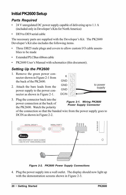
Setting Up the PK26001. Remove the green power con-
nector shown in Figure 2-1 fromthe back of the PK2600.
2. Attach the bare leads from thepower supply to the power con-nector as shown in Figure 2-1.
3. Plug the connector back into thepower connection at the back ofthe PK2600. Watch the polarityof the connection so that the banded wire from the power supply goes toDCIN as shown in Figure 2-2.
Figure 2-2. PK2600 Power Supply Connections
4. Plug the power supply into a wall outlet. The display should now light upwith the demonstration screens shown in Figure 2-3.
Figure 2-1. Wiring PK2600Power Supply Connector
GNDto power
supply
DCIN
GND
GND
K
POWER
DC
ING
ND
GN
DG
ND
K
PLC
BU
S E
XP
S/N:2900 SPAFFORD ST. DAVIS CA 956161-530-757-3737 WWW.ZWORLD.COM
DIGITAL GROUP 1 SERIAL PORT 3
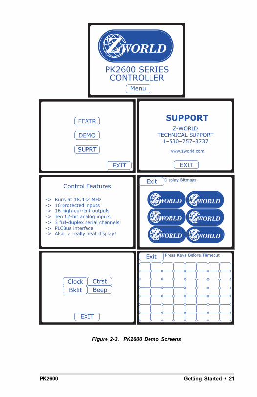
PK2600 Getting Started s 21
PK2600 SERIESCONTROLLER
Menu
FEATR
EXIT
SUPRT
DEMO
Control Features
-> Runs at 18.432 MHz-> 16 protected inputs-> 16 high-current outputs-> Ten 12-bit analog inputs-> 3 full-duplex serial channels-> PLCBus interface-> Alsoa really neat display!
Exit Display Bitmaps
Clock
EXIT
BklitCtrstBeep
Exit Press Keys Before Tiimeout
EXIT
SUPPORTZ-WORLD
TECHNICAL SUPPORT15307573737
www.zworld.com
Figure 2-3. PK2600 Demo Screens
PK260022 s Getting Started
(
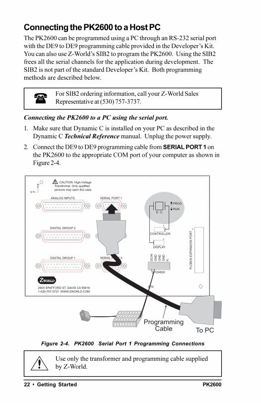
Connecting the PK2600 to a Host PCThe PK2600 can be programmed using a PC through an RS-232 serial portwith the DE9 to DE9 programming cable provided in the Developers Kit.You can also use Z-Worlds SIB2 to program the PK2600. Using the SIB2frees all the serial channels for the application during development. TheSIB2 is not part of the standard Developers Kit. Both programmingmethods are described below.
For SIB2 ordering information, call your Z-World SalesRepresentative at (530) 757-3737.
Connecting the PK2600 to a PC using the serial port.
1. Make sure that Dynamic C is installed on your PC as described in theDynamic C Technical Reference manual. Unplug the power supply.
2. Connect the DE9 to DE9 programming cable from SERIAL PORT 1 onthe PK2600 to the appropriate COM port of your computer as shown inFigure 2-4.
Figure 2-4. PK2600 Serial Port 1 Programming Connections
Use only the transformer and programming cable suppliedby Z-World.
PROG
RUN
CAUTION: High-VoltageTransformer. Only qualifiedpersons may open this case.
S/N:
CONTROLLER
POWER
DISPLAY
GN
DG
ND
DC
IN
KGN
D
PLC
BU
S E
XP
AN
SIO
N P
OR
T
DIGITAL GROUP 2
ANALOG INPUTS
DIGITAL GROUP 1
SERIAL PORT 1
SERIAL PORT 2
SERIAL PORT 3
D C
2900 SPAFFORD ST. DAVIS CA 956161-530-757-3737 WWW.ZWORLD.COM
H
V
ProgrammingCable To PC

PK2600 Getting Started s 23
!
PROG
RUN
CAUTION: High-VoltageTransformer. Only qualifiedpersons may open this case.
S/N:
CONTROLLER
POWER
DISPLAY
GN
DG
ND
DC
IN
KGN
D
PLC
BU
S E
XP
AN
SIO
N P
OR
T
DIGITAL GROUP 2
ANALOG INPUTS
DIGITAL GROUP 1
SERIAL PORT 1
SERIAL PORT 2
SERIAL PORT 3
D C
2900 SPAFFORD ST. DAVIS CA 956161-530-757-3737 WWW.ZWORLD.COM
H
V
To PC
MarkedConductor
to Pin 1
!
3. Set the C Run/Program switch on the back of the PK2600 to PROG.
4. Plug the power supply transformer into a wall socket.
Only the controller may be programmed at this time throughSERIAL PORT 1. The SIB2 is required to program the display.
Connecting the PK2600 controller to a PC using the SIB2.
1. Make sure that Dynamic C is installed on your PC as described in theDynamic C Technical Reference manual. Unplug the power supply.
2. Connect an RJ-12 cable between the RJ-12/DE9 adapter attached to thePC and the SIB2. The cable and adapter are supplied with the SIB2.
3. Plug the SIB2s 8-pin connector onto the CONTROLLER header locatedon the back of the PK2600, as shown in Figure 2-5. Make sure that pin 1on the ribbon cable connector (on the striped side) matches up withpin 1 on the CONTROLLER header (indicated by a small black dot next tothe header).
Figure 2-5. PK2600 SIB2 Programming Connections
4. Plug the power supply transformer into a wall socket.
The Run/Program switches must remain in the RUN positionwhen using the SIB2 to program the PK2600. The SIB2 takescare of setting the PK2600 to program mode while it is con-nected to the PK2600.

PK260024 s Getting Started
Connecting the PK2600 display to a PC using the SIB2.
1. Make sure that Dynamic C is installed on your PC as described in theDynamic C Technical Reference manual. Unplug the power supply.
2. Connect an RJ-12 cable between the RJ-12/DE9 adapter attached to thePC and the SIB2. The cable and adapter are supplied with the SIB2.
3. Plug the SIB2s 8-pin connector onto the DISPLAY header located on theback of the PK2600, as shown in Figure 2-5. Make sure that pin 1 on theribbon cable connector (on the striped side) matches up with pin 1 onthe DISPLAY header (indicated by a small black dot next to the header).
4. Plug the power supply transformer into a wall socket.
Running Dynamic CWith the SIB2 connected to the DISPLAY header, double-click the DynamicC icon to start the software. Note that the PC attempts to communicatewith the PK2600 each time Dynamic C is started. No error messages aredisplayed once communication is established.
The communication rate, port, and protocol are all selected by choosingSerial Options from Dynamic Cs OPTIONS menu. The SIB2 and thePK2600 both set their baud rate automatically to match the communicationrate set on the host PC using Dynamic C (9600 bps, 19,200 bps, 28,800 bpsor 57,600 bps). To begin, adjust the communications rate to 19,200 bps.
Make sure that the PC serial port used to connect the serial cable (COM1or COM2) is the one selected in the Dynamic C OPTIONS menu. Select the1-stop-bit protocol.
See Appendix A, Troubleshooting, if an error message suchas Target Not Responding or Communication Error appears.
Once the necessary changes have been made to establishcommunication between the host PC and the display board,use the Dynamic C shortcut <Ctrl Y> to reset the controller andinitiate communication.
At this point, the LCD should be blank and the backlight should be off.Once communication is established, load the sample program DEFDEMOL.C inthe Dynamic C SAMPLES\QVGA subdirectory. Compile and run the programby pressing F9 or by selecting Run from the Run menu.
The PK2600 should now alternately display the large font (17x × 35h) andthe small font (6w × 8h). The fonts should scroll across the display.
Compiling and running this sample program will overwrite theZ-World demonstration program shown in Figure 2-3.
$
!
!
PK2600 Hardware Features s 25
CHAPTER 3: HARDWARE FEATURES
Chapter 3 describes the PK2600 hardware. The following sections areincluded.
Operating Modes
Liquid Crystal Display
Keypad Interface
Digital Inputs/Outputs
Serial Channels
PLCBus

PK260026 s Hardware Features
Operating ModesThe PK2600 has two mutually exclusive operating modes, Run Mode andProgram Mode. Each mode is explained in detail below.
Program Mode
In Program mode, the PK2600 runs under the control of the PC that isrunning Dynamic C. The PK2600 must be in this mode to compile aprogram to the PK2600 or to debug a program. The PK2600 will run aprogram without polling when the PK2600 is in Program mode.
The Dynamic C manuals provide a complete description ofprogram polling.
In Program mode, the PK2600 matches the baud rate of the PCCOM port up to 57,600 bps.
Run Mode
In Run mode, the PK2600 runs standalone. At power-up, the PK2600checks to see if its onboard memory contains a program. If a programexists, the PK2600 executes the program immediately after power-up.
In Run mode, the PK2600 does not respond to Dynamic Crunning on the PC. A program cannot be compiled or de-bugged when the PK2600 is in Run mode.
The PK2600 has two DIP switchesto set the Run or Program modesone for the controller (C) and one forthe display (D).
Although the controllerand the display are pro-grammed separately,both DIP switchesshould be set to RUN forthe PK2600 to run stand-alone.
Figure 3-1 shows the location of theDIP switches used to set the Run orProgram modes.
$
!
!
Tip
Figure 3-1. Location of Run/Program
DIP Switches
CONTROLLER
DISPLAY
D CRUN
PROG
PK2600 Hardware Features s 27
Changing the Operating Mode1. Locate the Run/Program DIP switch (see Figure 3-1).
2. Select whether the display or the controller is to have its operatingmode changed, and set the corresponding DIP switch to the desiredoperating mode.
3. Cycle the power off and back on to switch the PK2600 to the selectedmode.
Using Run and Program Modes: Example1. Place the PK2600 display in Program mode and cycle the units power.
2. Select a sample program from the Dynamic C SAMPLES\QVGA directoryand open the program.
3. Select the Compile command from the Compile menu, or press F3 onthe PC keyboard.
4. If no errors are detected, Dynamic C compiles the program and auto-matically downloads it into the displays flash memory.
5. Return the DIP switch setting to Run mode, and cycle the power offand on to reset the PK2600. The downloaded program begins to runimmediately.
The program is now loaded in the PK2600 displays flash EPROM. Thisprogram runs automatically every time the PK2600 powers up in Run modeuntil you load another program.
Similar steps can be followed to download a program into the controllersflash memory.
The downloaded program begins to run as soon as the poweris applied. Pay close attention after downloading programsto the controller so that any electronic or mechanical devicesconnected to the PK2600 do not cause any damage.

PK260028 s Hardware Features
Liquid Crystal Display (LCD)The 240 × 320 ¼ VGA LCD supports both graphics and text. Automaticcontrast control is built in so that the contrast, once set, does not drift asthe PK2600 warms up or is moved.
Figure 3-2 provides a block diagram of the LCD control and RAM circuits.
Figure 3-2. Block Diagram LCD Control and Memory
The LCD is connected to the PK2600display circuit board through header J1or J3 on the display circuit board.
Contrast AdjustmentFigure 3-3 shows the location of themanual contrast adjustment access.Insert a small screwdriver to adjust thevariable resistor inside the enclosure.This contrast adjustment is the factorydefault for the PK2610. The PK2600 isconfigured with software contrast con-trol as the factory default. With soft-ware contrast control, the contrastlevel may be set via a software func-tion call. Since it is hard to guess thecorrect level in software, buttons de-fined on the touchscreen and in soft-ware can be used to adjust the con-trast.
U2
VCCVRAMCS1
A[0–14]
/CS
VCC
D[0–7]
RAM
U1
VCCVRAMCS2
A[0–14]
/CS
VCC
D[0–7]
RAM
U3
VA[0–14]
VD[0–7]
FRAME
ON/OFF
/RESET
SED1335FLCD Control
XD[0–3]
/INT0
D[0–7]
A0
FRAME
XD[0–3]
VCC
ON/OFF
LCDVEE
ADJUST
VCC
R2610 kΩ
R312.5 kΩ
-
+
Manual
Software ContrastAdjustment
PLC
BU
S E
XP
AN
SIO
N P
OR
T
CO
NTR
AST
MANUALCONTRAST
ADJUSTMENT
Figure 3-3. Location of PK2600Manual Contrast Adjustment
PK2600 Hardware Features s 29
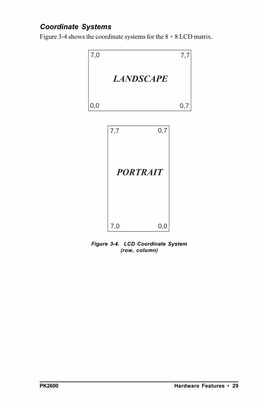
Coordinate SystemsFigure 3-4 shows the coordinate systems for the 8 × 8 LCD matrix.
Figure 3-4. LCD Coordinate System(row, column)
LANDSCAPE
0,7
7,0 7,7
0,0
PORTRAIT
0,7
7,0
7,7
0,0
PK260030 s Hardware Features
K
DIGITAL GROUP 2
HV
B00
HV
B01
HV
B02
HV
B03
HV
B04
HV
B08
HV
B05
HV
B06
HV
B07K
HV
B09
HV
B10
HV
B11
HV
B13
HV
B14
HV
B15
HV
B12
GN
D
KGN
DG
ND
K
GN
DG
ND
13 12 11 10 9 8 7 6 5 4 3 2 1
25 24 23 22 21 20 19 18 17 16 15 14
Digital Inputs/Outputs
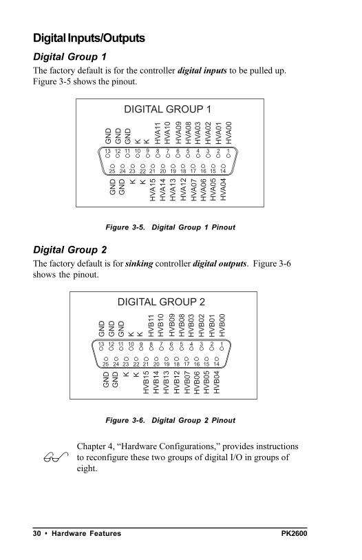
Digital Group 1The factory default is for the controller digital inputs to be pulled up.Figure 3-5 shows the pinout.
Figure 3-5. Digital Group 1 Pinout
Digital Group 2The factory default is for sinking controller digital outputs. Figure 3-6shows the pinout.
Figure 3-6. Digital Group 2 Pinout
Chapter 4, Hardware Configurations, provides instructionsto reconfigure these two groups of digital I/O in groups ofeight.
K
DIGITAL GROUP 1
HV
A00
HV
A01
HV
A02
HV
A03
HV
A04
HV
A08
HV
A05
HV
A06
HV
A07K
HV
A09
HV
A10
HV
A11
HV
A13
HV
A14
HV
A15
HV
A12
GN
D
KGN
DG
ND
K
GN
DG
ND
13 12 11 10 9 8 7 6 5 4 3 2 1
25 24 23 22 21 20 19 18 17 16 15 14
$
PK2600 Hardware Features s 31
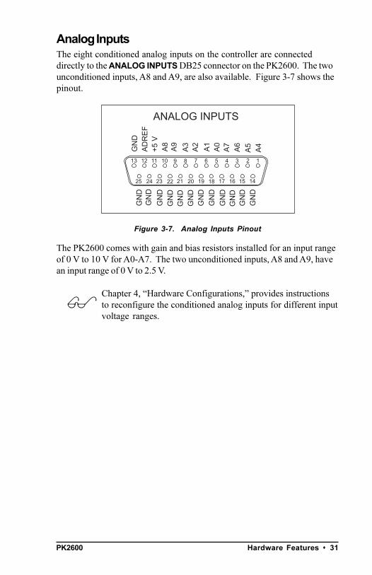
Analog InputsThe eight conditioned analog inputs on the controller are connecteddirectly to the ANALOG INPUTS DB25 connector on the PK2600. The twounconditioned inputs, A8 and A9, are also available. Figure 3-7 shows thepinout.
Figure 3-7. Analog Inputs Pinout
The PK2600 comes with gain and bias resistors installed for an input rangeof 0 V to 10 V for A0-A7. The two unconditioned inputs, A8 and A9, havean input range of 0 V to 2.5 V.
Chapter 4, Hardware Configurations, provides instructionsto reconfigure the conditioned analog inputs for different inputvoltage ranges.
GN
D
ANALOG INPUTS
A4
A5A6
A7
GN
D
A0
GN
DG
ND
GN
D
GN
D
A1
A2
A3
GN
DG
ND
GN
D
GN
D
GN
D
A8
AD
RE
F+5
V
A9
GN
DG
ND
13 12 11 10 9 8 7 6 5 4 3 2 1
25 24 23 22 21 20 19 18 17 16 15 14
$
PK260032 s Hardware Features
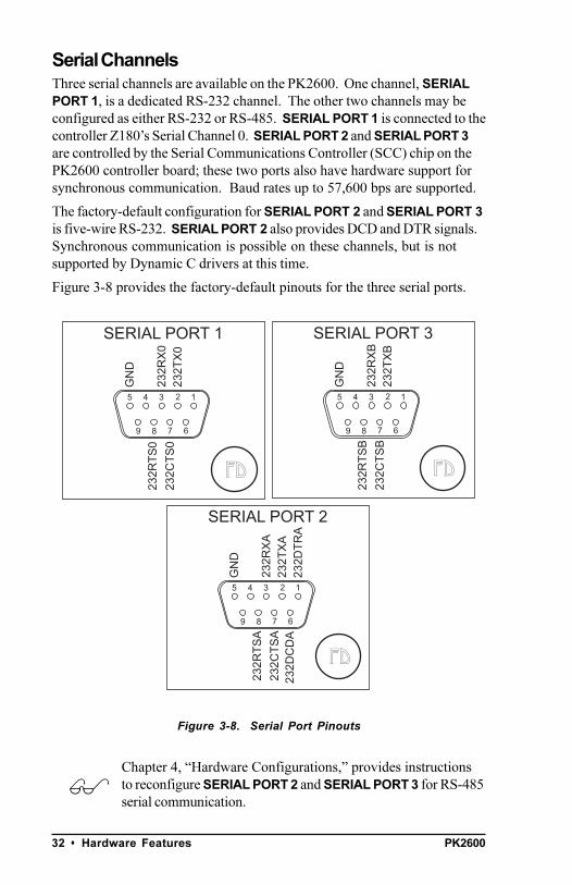
Serial ChannelsThree serial channels are available on the PK2600. One channel, SERIALPORT 1, is a dedicated RS-232 channel. The other two channels may beconfigured as either RS-232 or RS-485. SERIAL PORT 1 is connected to thecontroller Z180s Serial Channel 0. SERIAL PORT 2 and SERIAL PORT 3are controlled by the Serial Communications Controller (SCC) chip on thePK2600 controller board; these two ports also have hardware support forsynchronous communication. Baud rates up to 57,600 bps are supported.
The factory-default configuration for SERIAL PORT 2 and SERIAL PORT 3is five-wire RS-232. SERIAL PORT 2 also provides DCD and DTR signals.Synchronous communication is possible on these channels, but is notsupported by Dynamic C drivers at this time.
Figure 3-8 provides the factory-default pinouts for the three serial ports.
Figure 3-8. Serial Port Pinouts
Chapter 4, Hardware Configurations, provides instructionsto reconfigure SERIAL PORT 2 and SERIAL PORT 3 for RS-485serial communication.
SERIAL PORT 1
GN
D
232R
X0
232T
X0
232C
TS
023
2RT
S0
5 4 3 2 1
9 8 7 6
SERIAL PORT 2
GN
D
232R
XA
232T
XA
232C
TS
A23
2RT
SA
5 4 3 2 1
9 8 7 6
232D
TR
A23
2DC
DA
SERIAL PORT 3G
ND
232R
XB
232T
XB
232C
TS
B23
2RT
SB
5 4 3 2 1
9 8 7 6
FD FD
FD
$

PK2600 Hardware Features s 33
$
PLCBusThe PLCBus connector on the PK2600 allows expansion boards to beconnected to the PK2600. Expansion boards allow additional I/O, A/Dconverters, D/A converters, relay boards, and stepper motor controllers tobe connected to the PK2600.
Refer to Appendix E, PLCBus, for more detailed informationon the PLCBus and Z-Worlds expansion boards.

PK260034 s Hardware Features
Blank
PK2600 Hardware Configurations s 35
CHAPTER 4:
HARDWARE CONFIGURATIONS
Chapter 4 describes alternative hardware configurations for the PK2600.The back cover of the PK2600 must be removed, and some boards need tobe taken apart to access the appropriate configuration jumpers. Thefollowing sections are included.
PK2600 Assembly
Digital Inputs and Outputs
Analog inputs
Serial Channels
PLCBus
Liquid Crystal Display
PK260036 s Hardware Configurations
(
The configurations described in Chapter 3 are the factory-default configu-rations. The configurations are available without having to open thePK2600 enclosure.
Other configurations are possible, and are described in this chapter.
Z-World offers the PK2600 for quantity orders with theseother configurations set at the factory. For orderinginformation, call your Z-World Sales Representative at(530) 757-3737.
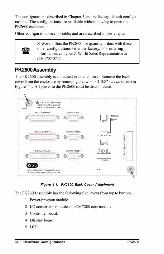
PK2600 AssemblyThe PK2600 assembly is contained in an enclosure. Remove the backcover from the enclosure by removing the two 4 x 1-3/8" screws shown inFigure 4-1. All power to the PK2600 must be disconnected.
Figure 4-1. PK2600 Back Cover Attachment
The PK2600 assembly has the following five layers from top to bottom.
1. Power/program module.
2. I/O conversion module and CM7200 core module.
3. Controller board.
4. Display board.
5. LCD.
PROG
RUN
CAUTION: High-VoltageTransformer. Only qualifiedpersons may open this case.
S/N:
CONTROLLER
POWER
DISPLAY
GN
DG
ND
DC
IN
KGN
D
PLC
BU
S E
XP
AN
SIO
N P
OR
T
DIGITAL GROUP 2
SERIAL PORT 1
SERIAL PORT 2
SERIAL PORT 3
D C
H
V
2900 SPAFFORD ST. DAVIS CA 956161-530-757-3737 WWW.ZWORLD.COM
DIGITAL GROUP 1
ANALOG INPUTS
PK2600 Hardware Configurations s 37
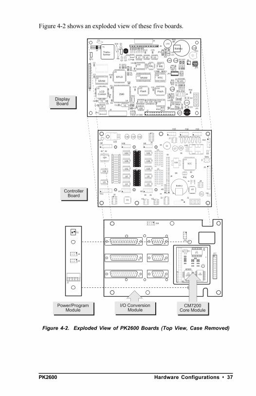
Figure 4-2 shows an exploded view of these five boards.
Figure 4-2. Exploded View of PK2600 Boards (Top View, Case Removed)
DisplayBoard
U6
Z180
EPLD
U5
Y2
’691PAL
FlashU16
RTCU14
L2
C44
C47
C38
C48
C36C35
Y1
U10
U7 U8 U9
U15
Flash
U17 U19
R15
C34
C28 R21
C27
RN3 C45
C46
R27
R28
JP4
J7
U11
SRAMU2
R32
J11
D1
D2
R29
R30
C42
C40
U27
U25
U21U22
R31R17
RN2
U12
C30C29
D3
Battery
C39
C37
R6
R7
R8
R11
C9
R10
R12
R5
J6
J5
RN1
L1
Q3Q2
Q1R30
R4
Trans-former
C2
C3
C4
U3 C41
R2
C1
J2
T1
J4 SIB2
J1
U13SRAM
JP1
C7C5
LCDControl C6
R1
C10
U4
J3
C12
R14
C31
C13
R13
C32
C33
U28 2954Reg.
C43
C11
C26
C25
MV1 MV2 J9
U26
JP3 U24
J8
RS-232
R16
R20
JP2C23C22
C14
C16
C15
C18
C17
C19
C20
C21
C24
R9
C8
LS1
R22
R24
R23
R25
R26
RT1
U23
U18
U20
ControllerBoard
Battery
SCC
H1
J5
H4C1
J4
U2
D1
U13
U14
J6
H5
U20
MV1MV2MV3MV4MV5MV6
C7
H13H14H15
J8
L1
J7
C6
C12C13C14
J3
H3 H2 J2
RN1
H12
J1
SW1
D2
U9
U12
U19
U4
U8
U11
U18
U22
H10H8
U24U23
U17
U7
H9
H6H7
U15
U5
U1
U3
U6
U10
U16
U21
JP1
U2RAM
U3Flash
EPROM
U1RTC
H2
H1
J1
J2
J3
J4
J5
J6
J17
J18
J19
CM7200Core Module
I/O ConversionModule
Power/ProgramModule
H11
S1
J4
J3
J2
PK260038 s Hardware Configurations
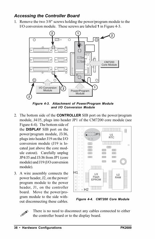
Accessing the Controller Board1. Remove the two 3/8" screws holding the power/program module to the
I/O conversion module. These screws are labeled 1 in Figure 4-3.
Figure 4-3. Attachment of Power/Program Moduleand I/O Conversion Module
2. The bottom side of the CONTROLLER SIB port on the power/programmodule, J4/J5, plugs into header JP1 of the CM7200 core module (seeFigure 4-4). The bottom side ofthe DISPLAY SIB port on thepower/program module, J3/J6,plugs into header J19 on the I/Oconversion module (J19 is lo-cated just above the core mod-ule cutout). Carefully unplugJP4/J5 and J3/J6 from JP1 (coremodule) and J19 (I/O conversionmodule).
3. A wire assembly connects thepower header, J2, on the power/program module to the powerheader, J1, on the controllerboard. Move the power/pro-gram module to the side with-out disconnecting these cables.
There is no need to disconnect any cables connected to eitherthe controller board or to the display board.
JP1
U2RAM
U3Flash
EPROM
U1RTC
H2
H1
J1
J2
J3
J4
J5
J6
J17
J18
J19
CM7200Core Module
I/O ConversionModule Power/Program
Module
S1
J4
J3
J2
1
12
2
2
2
JP1
U2RAM
U3Flash
EPROM
U1RTC
H2
H1
Figure 4-4. CM7200 Core Module
!

PK2600 Hardware Configurations s 39
4. Remove the four 4 x 3/4" screws holding the I/O conversion module tothe PK2600 assembly. These screws are labeled 2 in Figure 4-3.
5. The I/O conversion module plugs into headers H8H11, H7H10, H6H9, J5, H12, H14 and H15 on the controller board. Carefully unplug theI/O conversion from these headers. Figure 4-5 shows the headerlocations on the controller board.
Figure 4-5. Attachment of Controller Board to Display Boardand I/O Conversion Module
The CM7200 core module is attached to the controller board.There is no need to remove the core module to access eitherthe controller board or the display board.
All headers and jumpers necessary to configure the controller board arenow accessible. Once the controller board has been reconfigured, repeatthe above steps in reverse order, or remove the controller board to gainaccess to the display board.
Battery
SCC
H1
J5
H4C1
J4
U2
D1
U13
U14
J6
H5
U20
MV1MV2MV3MV4MV5MV6
C7
H13H14H15
J8
L1
J7
C6
C12C13C14
J3
H3 H2 J2
RN1
H12
J1
SW1
D2
U9
U12
U19
U4
U8
U11
U18
U22
H10H8
U24U23
U17
U7
H9
H6H7
U15
U5
U1
U3
U6
U10
U16
U21
JP1
U2RAM
U3Flash
EPROM
U1RTC
H2
H1
Remove toaccess
Display Board
ControllerBoard
H11
Standoffs
Remove toaccess
Display Board
CM7200Core Module
!
PK260040 s Hardware Configurations
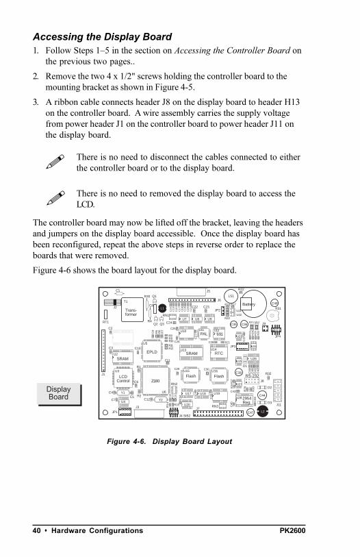
Accessing the Display Board1. Follow Steps 15 in the section on Accessing the Controller Board on
the previous two pages..
2. Remove the two 4 x 1/2" screws holding the controller board to themounting bracket as shown in Figure 4-5.
3. A ribbon cable connects header J8 on the display board to header H13on the controller board. A wire assembly carries the supply voltagefrom power header J1 on the controller board to power header J11 onthe display board.
There is no need to disconnect the cables connected to eitherthe controller board or to the display board.
There is no need to removed the display board to access theLCD.
The controller board may now be lifted off the bracket, leaving the headersand jumpers on the display board accessible. Once the display board hasbeen reconfigured, repeat the above steps in reverse order to replace theboards that were removed.
Figure 4-6 shows the board layout for the display board.
Figure 4-6. Display Board Layout
!
!
DisplayBoard
U6
Z180
EPLD
U5
Y2
’691PAL
FlashU16
RTCU14
L2
C44
C47
C38
C48
C36C35
Y1
U10
U7 U8 U9
U15
Flash
U17 U19
R15
C34
C28 R21
C27
RN3 C45
C46
R27
R28
JP4
J7
U11
SRAMU2
R32
J11
D1
D2
R29
R30
C42
C40
U27
U25
U21U22
R31R17
RN2
U12
C30C29
D3
Battery
C39
C37
R6
R7
R8
R11
C9
R10
R12
R5
J6
J5
RN1
L1
Q3Q2
Q1R30
R4
Trans-former
C2
C3
C4
U3 C41
R2
C1
J2
T1
J4 SIB2
J1
U13SRAM
JP1
C7C5
LCDControl C6
R1
C10
U4
J3
C12
R14
C31
C13
R13
C32
C33
U28 2954Reg.
C43
C11
C26
C25
MV1 MV2 J9
U26
JP3 U24
J8
RS-232
R16
R20
JP2C23C22
C14
C16
C15
C18
C17
C19
C20
C21
C24
R9
C8
LS1
R22
R24
R23
R25
R26
RT1
U23
U18
U20
PK2600 Hardware Configurations s 41
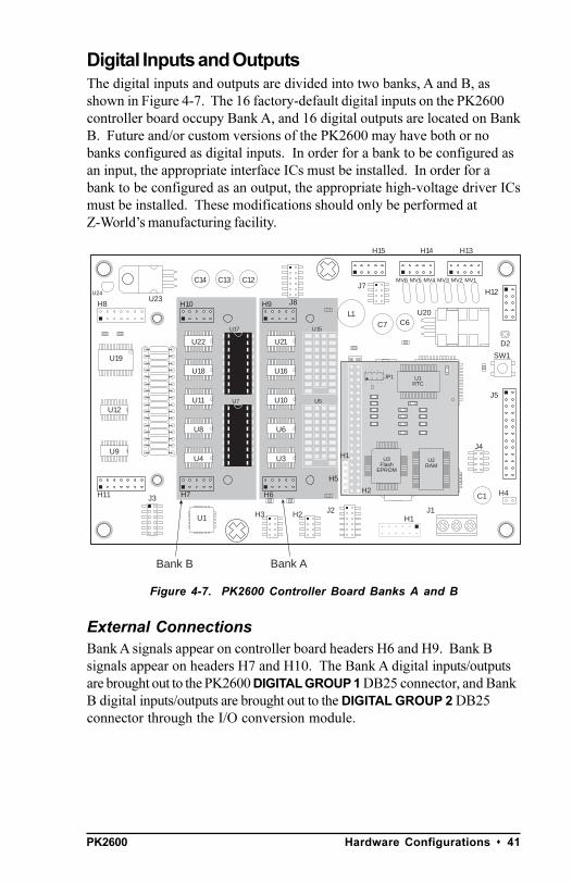
Digital Inputs and OutputsThe digital inputs and outputs are divided into two banks, A and B, asshown in Figure 4-7. The 16 factory-default digital inputs on the PK2600controller board occupy Bank A, and 16 digital outputs are located on BankB. Future and/or custom versions of the PK2600 may have both or nobanks configured as digital inputs. In order for a bank to be configured asan input, the appropriate interface ICs must be installed. In order for abank to be configured as an output, the appropriate high-voltage driver ICsmust be installed. These modifications should only be performed atZ-Worlds manufacturing facility.
Figure 4-7. PK2600 Controller Board Banks A and B
External ConnectionsBank A signals appear on controller board headers H6 and H9. Bank Bsignals appear on headers H7 and H10. The Bank A digital inputs/outputsare brought out to the PK2600 DIGITAL GROUP 1 DB25 connector, and BankB digital inputs/outputs are brought out to the DIGITAL GROUP 2 DB25connector through the I/O conversion module.
Bank B Bank A
H11
Battery
SCC
H1
J5
H4C1
J4
U2
D1
U13
U14
J6
H5
U20
MV1MV2MV3MV4MV5MV6
C7
H13H14H15
J8
L1
J7
C6
C12C13C14
J3
H3 H2 J2
RN1
H12
J1
SW1
D2
U9
U12
U19
U4
U8
U11
U18
U22
H10H8
U24U23
U17
U7
H9
H6H7
U15
U5
U1
U3
U6
U10
U16
U21
JP1
U2RAM
U3Flash
EPROM
U1RTC
H2
H1
PK260042 s Hardware Configurations
Digital InputsThe PK2600 can provide up to 32 protected digital inputs designed aslogical data inputs, returning a 1 or 0. Their normal operating range is -20 VDC to +24 V DC, and they are protected from voltages between -48 V DCand +48 V DC. The inputs can detect logic-level signals and have anominal logic threshold of 2.5 V DC. This means an input returns a 0 if theinput voltage is below 2.5 V DC and a 1 if the input voltage is above 2.5 VDC. The inputs can be pulled up to +5 V or down to ground.
A low-pass filter on each input channel has a time constant of
TRC
= 220 µs (4.5 kHz).
The digital inputs may be configured as pull-up or pull-down in groups offours and eights. The configuration of each input should be determined bynormal operating conditions, power-down mode and possible failure modesincluding open or shorted conditions. These factors will influence yourdecision about configuring the inputs as pull-up or pull-down.
Operating Modes and ConfigurationInputs may be pulled up to +5 V or pulled down to ground by configuringthe jumpers on the PK2600 controller board headers J2 and J3.
J2 jumpers select pull-up/pull-down resistors for Bank A. Jumpers on J3select pull-up/pull-down resistors for inputs for Bank B. To change aninput from the factory default of pull-up, simply place a jumper across theappropriate two pins of J2 and/or J3.
Tables 4-1 and 4-2 illustrate the jumper settings for pull-up and pull-downconfigurations for the controller boards Bank A and Bank B inputs.
The factory default is for the digital inputs to be pulled up to+5 V.FD
PK2600 Hardware Configurations s 43
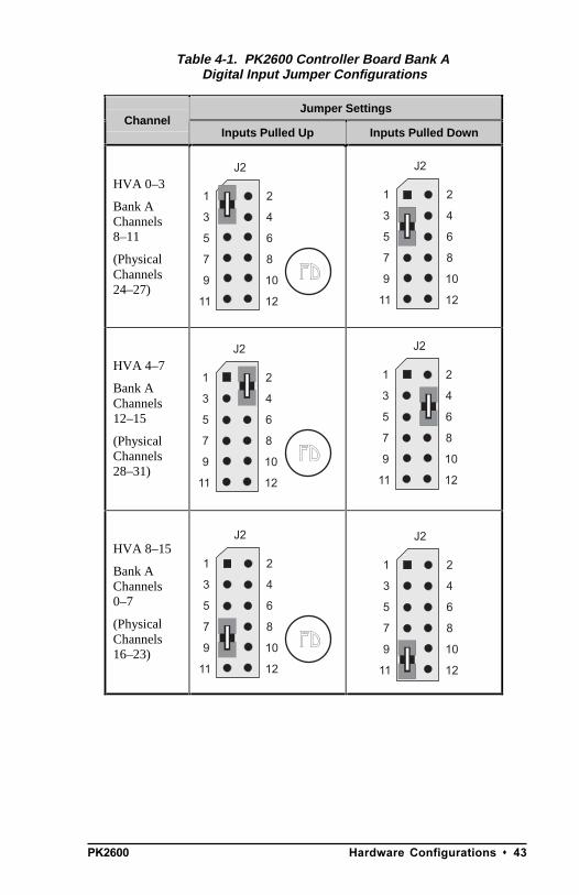
Table 4-1. PK2600 Controller Board Bank A Digital Input Jumper Configurations
Jumper SettingsChannel
Inputs Pulled Up Inputs Pulled Down
HVA 0–3
Bank AChannels8–11
(PhysicalChannels24–27)
HVA 4–7
Bank AChannels12–15
(PhysicalChannels28–31)
HVA 8–15
Bank AChannels0–7
(PhysicalChannels16–23)
10
12
J2
1 2
3 4
5 6
7 8
9
11
FD
10
12
J2
1 2
3 4
5 6
7 8
9
11
FD
10
12
J2
1 2
3 4
5 6
7 8
9
11
FD
10
12
J2
1 2
3 4
5 6
7 8
9
11
10
12
J2
1 2
3 4
5 6
7 8
9
11
10
12
J2
1 2
3 4
5 6
7 8
9
11
PK260044 s Hardware Configurations
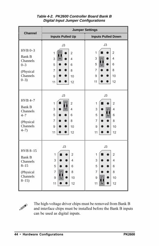
The high-voltage driver chips must be removed from Bank Band interface chips must be installed before the Bank B inputscan be used as digital inputs.
!
Table 4-2. PK2600 Controller Board Bank BDigital Input Jumper Configurations
Jumper SettingsChannel
Inputs Pulled Up Inputs Pulled Down
HVB 0–3
Bank BChannels0–3
(PhysicalChannels0–3)
HVB 4–7
Bank BChannels4–7
(PhysicalChannels4–7)
HVB 8–15
Bank BChannels8–15
(PhysicalChannels8–15)
10
12
J3
1 2
3 4
5 6
7 8
9
11
10
12
J3
1 2
3 4
5 6
7 8
9
11
10
12
J3
1 2
3 4
5 6
7 8
9
11
10
12
J3
1 2
3 4
5 6
7 8
9
11
10
12
J3
1 2
3 4
5 6
7 8
9
11
10
12
J3
1 2
3 4
5 6
7 8
9
11

PK2600 Hardware Configurations s 45
Digital OutputsUp to 32 high-voltage, high-current digital outputs are possible on thePK2600. The digital outputs can be configured in groups of eight for eithersinking or sourcing operation by setting jumpers and installing theappropriate driver ICs. Sinking drivers can sink up to 500 mA at voltagesup to 48 V DC. Sourcing drivers can source up to 250 mA at voltages up to30 V DC. All outputs are diode protected against inductive spikes.
TTL/CMOS level outputs are also possible by bypassing the driver ICs.This option is for quantity orders only, and should be performed atZ-Worlds manufacturing facility.
High-voltage outputs are diode protected against inductive spikes. Alloutputs are individually addressable.
Operating Modes and ConfigurationThe digital inputs and outputs are divided into two banks, Bank A andBank B. In the factory default, digital outputs occupy Bank B and digitalinputs are located on Bank A. In order for a bank to be configured as anoutput, the appropriate interface ICs must be installed. Z-World recom-mends that this be done only at Z-Worlds manufacturing facility.
High-Voltage DriversOutputs may be configured for either sinking or sourcing current. Theconfiguration is determined by the type of driver ICs installed and thejumper settings.
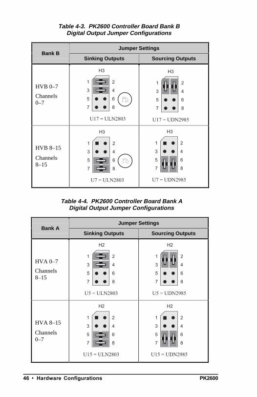
For Bank A, U5 drives outputs 8-15 and U15 drives outputs 07. ForBank B, U7 drives outputs 8-15 and U17 drives outputs 07. The jumpersplaced on H3 configure sourcing/sinking modes for the outputs on Bank B.Jumpers on H2 configure sourcing/sinking modes for the outputs on BankA (if it is configured for output). Tables 4-3 and 4-4 show the jumpersettings for sinking and sourcing configurations.
The sinking driver chips used on the PK2600 controller board are ULN2803or equivalent. The sourcing driver chips are UDN2985 or equivalent.
To configure drivers for sinking outputs (default for Bank B), install theULN2803 driver chips in the appropriate socket locations. For sourcingoutputs, install UDN2985 driver chips.
PK260046 s Hardware Configurations
Table 4-3. PK2600 Controller Board Bank BDigital Output Jumper Configurations
Jumper SettingsBank B
Sinking Outputs Sourcing Outputs
HVB 0–7
Channels0–7
HVB 8–15
Channels8–15
H3
1 2
3 4
5 6
7 8
U17 = ULN2803
FD
H3
1 2
3 4
5 6
7 8
U17 = UDN2985
H3
1 2
3 4
5 6
7 8
U7 = ULN2803
FD
H3
1 2
3 4
5 6
7 8
U7 = UDN2985
Table 4-4. PK2600 Controller Board Bank ADigital Output Jumper Configurations
Jumper SettingsBank A
Sinking Outputs Sourcing Outputs
HVA 0–7
Channels8–15
HVA 8–15
Channels0–7
H2
1 2
3 4
5 6
7 8
U5 = ULN2803
H2
1 2
3 4
5 6
7 8
U5 = UDN2985
H2
1 2
3 4
5 6
7 8
U15 = ULN2803
H2
1 2
3 4
5 6
7 8
U15 = UDN2985
PK2600 Hardware Configurations s 47
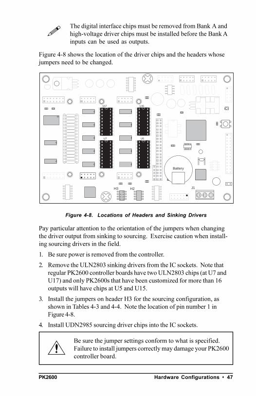
The digital interface chips must be removed from Bank A andhigh-voltage driver chips must be installed before the Bank Ainputs can be used as outputs.
Figure 4-8 shows the location of the driver chips and the headers whosejumpers need to be changed.
Figure 4-8. Locations of Headers and Sinking Drivers
Pay particular attention to the orientation of the jumpers when changingthe driver output from sinking to sourcing. Exercise caution when install-ing sourcing drivers in the field.
1. Be sure power is removed from the controller.
2. Remove the ULN2803 sinking drivers from the IC sockets. Note thatregular PK2600 controller boards have two ULN2803 chips (at U7 andU17) and only PK2600s that have been customized for more than 16outputs will have chips at U5 and U15.
3. Install the jumpers on header H3 for the sourcing configuration, asshown in Tables 4-3 and 4-4. Note the location of pin number 1 inFigure 4-8.
4. Install UDN2985 sourcing driver chips into the IC sockets.
Be sure the jumper settings conform to what is specified.Failure to install jumpers correctly may damage your PK2600controller board.
Battery
H3 J1
U17
U7
U15
U5
H2
!
PK260048 s Hardware Configurations
(
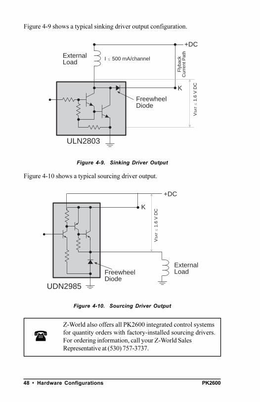
Figure 4-9 shows a typical sinking driver output configuration.
Figure 4-9. Sinking Driver Output
Figure 4-10 shows a typical sourcing driver output.
Figure 4-10. Sourcing Driver Output
Z-World also offers all PK2600 integrated control systemsfor quantity orders with factory-installed sourcing drivers.For ordering information, call your Z-World SalesRepresentative at (530) 757-3737.
ULN2803
K
ExternalLoad
FreewheelDiode
+DC
I # 500 mA/channel
Fly
back
Cur
rent
Pat
h
VS
AT #
1.6
V D
C
ExternalLoad
UDN2985
K
+DC
FreewheelDiode
VS
AT #
1.6
V D
C

PK2600 Hardware Configurations s 49
Connections to Bank A are made on headers H6 and H9. Connections toBank B are made on headers H7 and H10. The pinouts for headers H6, H7,H9 and H10 are shown in Figure 4-7.
See Appendix B, Specifications, for detailed specificationson the high-voltage drivers.
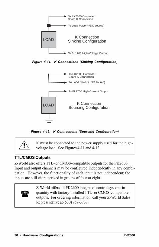
Using Output DriversThe common supply for all eight channels supplied by a driver chip iscalled K, and is labeled as such on the PK2600 pinouts. K must bepowered up to allow proper operation.
The K connection performs two vital functions to the high-voltage drivercircuitry on the PK2600.
1. K supplies power to driver circuitry inside the driver chip.
2. K also allows a diode internal to the driver chip to snub voltagetransients produced during the inductive kick associated with switch-ing inductive loads. (Relays, solenoids, and speakers are examples ofinductive loads.)
Long leads may present enough induction to also produce large potentiallydamaging voltage transients. The anodes of the protection diodes foreach channel are common, and so only one voltage supply can be used forall high-voltage driver loads.
The following points summarize the functions of K.
K provides power to the driver chip circuitry.
K provides clamping for all high-voltage driver loads.
It is mandatory to connect K regardless of whether sourcing or sinking.
The loads supply must have a common ground with all other suppliesin your system.
All loads must use same supply voltage.
Refer to Figures 4-11 and 4-12 when connecting K.
$
PK260050 s Hardware Configurations
(
Figure 4-11. K Connections (Sinking Configuration)
Figure 4-12. K Connections (Sourcing Configuration)
K must be connected to the power supply used for the high-voltage load. See Figures 4-11 and 4-12.
TTL/CMOS OutputsZ-World also offers TTL- or CMOS-compatible outputs for the PK2600.Input and output channels may be configured independently in any combi-nation. However, the functionality of each input is not independent; theinputs are still characterized in groups of four or eight.
Z-World offers all PK2600 integrated control systems inquantity with factory-installed TTL- or CMOS-compatibleoutputs. For ordering information, call your Z-World SalesRepresentative at (530) 757-3737.
To PK2600 ControllerBoard K Connection
To BL1700 High-Voltage Output
LOAD
To Load Power (+DC source)
K ConnectionSinking Configuration
To PK2600 ControllerBoard K Connection
To BL1700 High-Current Output
K ConnectionSourcing Configuration
LOAD
To Load Power (+DC source)
PK2600 Hardware Configurations s 51
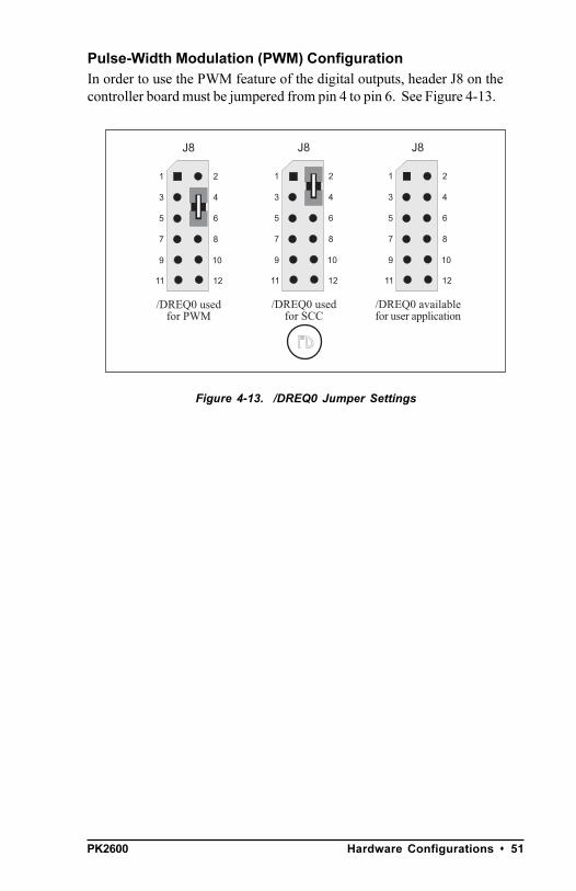
Pulse-Width Modulation (PWM) ConfigurationIn order to use the PWM feature of the digital outputs, header J8 on thecontroller board must be jumpered from pin 4 to pin 6. See Figure 4-13.
Figure 4-13. /DREQ0 Jumper Settings
10
J8
1 2
3 4
5 6
7 8
9
1211
/DREQ0 usedfor PWM
10
J8
1 2
3 4
5 6
7 8
9
1211
/DREQ0 usedfor SCC
10
J8
1 2
3 4
5 6
7 8
9
1211
/DREQ0 availablefor user application
FD
PK260052 s Hardware Configurations
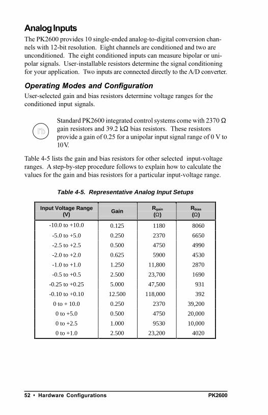
Analog InputsThe PK2600 provides 10 single-ended analog-to-digital conversion chan-nels with 12-bit resolution. Eight channels are conditioned and two areunconditioned. The eight conditioned inputs can measure bipolar or uni-polar signals. User-installable resistors determine the signal conditioningfor your application. Two inputs are connected directly to the A/D converter.
Operating Modes and ConfigurationUser-selected gain and bias resistors determine voltage ranges for theconditioned input signals.
Standard PK2600 integrated control systems come with 2370 Ωgain resistors and 39.2 kΩ bias resistors. These resistorsprovide a gain of 0.25 for a unipolar input signal range of 0 V to10 V.
Table 4-5 lists the gain and bias resistors for other selected input-voltageranges. A step-by-step procedure follows to explain how to calculate thevalues for the gain and bias resistors for a particular input-voltage range.
FD
Table 4-5. Representative Analog Input Setups
Input Voltage Range(V) Gain
Rgain
(Ω)Rbias
(Ω)
-10.0 to +10.0 0.125 1180 8060
-5.0 to +5.0 0.250 2370 6650
-2.5 to +2.5 0.500 4750 4990
-2.0 to +2.0 0.625 5900 4530
-1.0 to +1.0 1.250 11,800 2870
-0.5 to +0.5 2.500 23,700 1690
-0.25 to +0.25 5.000 47,500 931
-0.10 to +0.10 12.500 118,000 392
0 to + 10.0 0.250 2370 39,200
0 to +5.0 0.500 4750 20,000
0 to +2.5 1.000 9530 10,000
0 to +1.0 2.500 23,200 4020
PK2600 Hardware Configurations s 53
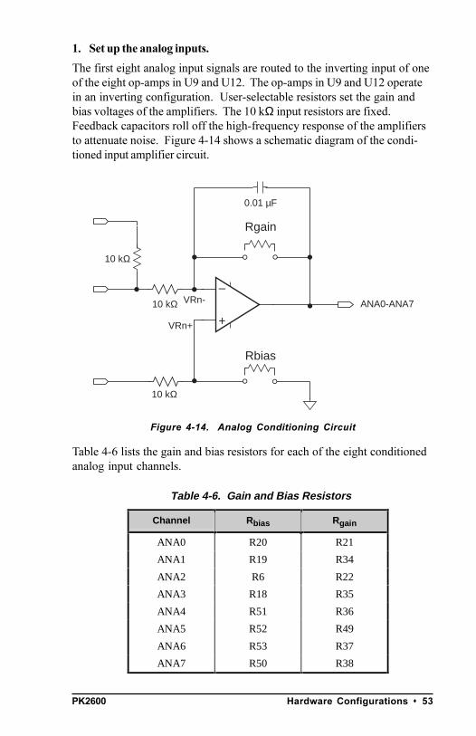
1. Set up the analog inputs.
The first eight analog input signals are routed to the inverting input of oneof the eight op-amps in U9 and U12. The op-amps in U9 and U12 operatein an inverting configuration. User-selectable resistors set the gain andbias voltages of the amplifiers. The 10 kΩ input resistors are fixed.Feedback capacitors roll off the high-frequency response of the amplifiersto attenuate noise. Figure 4-14 shows a schematic diagram of the condi-tioned input amplifier circuit.
Figure 4-14. Analog Conditioning Circuit
Table 4-6 lists the gain and bias resistors for each of the eight conditionedanalog input channels.
ANA0-ANA7+
–
10 kΩ
10 kΩ
10 kΩ
0.01 µF
Rgain
Rbias
VRn+
VRn-
Table 4-6. Gain and Bias Resistors
Channel Rbias Rgain
ANA0 R20 R21
ANA1 R19 R34
ANA2 R6 R22
ANA3 R18 R35
ANA4 R51 R36
ANA5 R52 R49
ANA6 R53 R37
ANA7 R50 R38

PK260054 s Hardware Configurations
(
Strip sockets spaced 0.400 inches (10.2 mm) apart accommodate the gainand bias resistors.
Z-World can install surface-mounted gain and bias resistorsfor your exact configuration in production quantities. For moreinformation, call your Z-World Sales Representative at (530)757-3737.
2. Select gain resistor.
The gain and bias resistors determine the input signals voltage relative toground as well as its range. For example, assume your circuit must handlean input signal voltage range of 10 V spanning -5 V to +5 V. You shouldfirst select the gain (feedback) resistor to suit an input signal voltage rangeof 10 V.
The gain of the amplifier is the ratio of its maximum output-voltage swingto your applications maximum input-voltage swing. The 2.5 V input-voltage range of the A/D chip limits the op-amps output swing to 2.5 V.Therefore, Equation (4-1) expresses an amplifiers gain in terms of its input-voltage range.
where g is the gain, VINmax is the maximum input voltage and VINmin
is theminimum input voltage.
The ratio of the user-specified gain resistor Rgain
to its associated fixedinput resistor determines an amplifiers gain. For the amplifier in Fig-ure 4-14 with its input resistor fixed at 10 kΩ, the gain is
Given an input voltage range of 10 V, this gain equation fixes the amplifiersgain at 0.25. This gain scales the input signals range properly down to theop-amps 2.5 V maximum output range. R
gain must therefore be 2500 Ω.
3. Determine bias resistor.
If the op-amp is to servo its output properly around the desired centervoltage, you must establish the appropriate bias voltage at the op-ampsnoninverting input. You must select the bias, or offset, resistor, R
bias, to
position the input-voltage range correctly with respect to ground. For thisexample, let us use -5 V to +5 V.
minmax ININ VV
V2.5g
−= (4-1)
.10,000
Rg
gain
Ω= (4-2)
PK2600 Hardware Configurations s 55
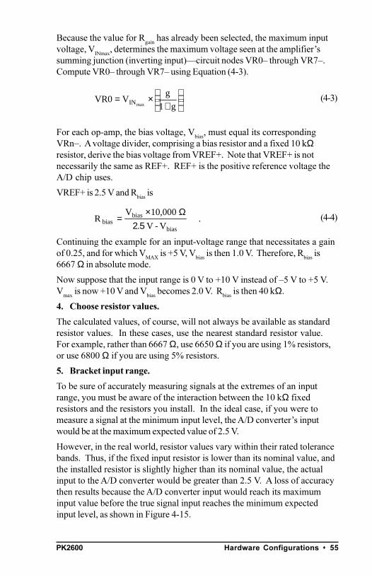
Because the value for Rgain
has already been selected, the maximum inputvoltage, V
INmax, determines the maximum voltage seen at the amplifiers
summing junction (inverting input)circuit nodes VR0 through VR7.Compute VR0 through VR7 using Equation (4-3).
For each op-amp, the bias voltage, Vbias, must equal its correspondingVRn. A voltage divider, comprising a bias resistor and a fixed 10 kΩresistor, derive the bias voltage from VREF+. Note that VREF+ is notnecessarily the same as REF+. REF+ is the positive reference voltage theA/D chip uses.
VREF+ is 2.5 V and Rbias
is
Continuing the example for an input-voltage range that necessitates a gainof 0.25, and for which V
MAX is +5 V, V
bias is then 1.0 V. Therefore, R
bias is
6667 Ω in absolute mode.
Now suppose that the input range is 0 V to +10 V instead of 5 V to +5 V.V
max is now +10 V and V
bias becomes 2.0 V. R
bias is then 40 kΩ.
4. Choose resistor values.
The calculated values, of course, will not always be available as standardresistor values. In these cases, use the nearest standard resistor value.For example, rather than 6667 Ω, use 6650 Ω if you are using 1% resistors,or use 6800 Ω if you are using 5% resistors.
5. Bracket input range.
To be sure of accurately measuring signals at the extremes of an inputrange, you must be aware of the interaction between the 10 kΩ fixedresistors and the resistors you install. In the ideal case, if you were tomeasure a signal at the minimum input level, the A/D converters inputwould be at the maximum expected value of 2.5 V.
However, in the real world, resistor values vary within their rated tolerancebands. Thus, if the fixed input resistor is lower than its nominal value, andthe installed resistor is slightly higher than its nominal value, the actualinput to the A/D converter would be greater than 2.5 V. A loss of accuracythen results because the A/D converter input would reach its maximuminput value before the true signal input reaches the minimum expectedinput level, as shown in Figure 4-15.
+
×=g1
gVVR0
maxIN (4-3)
.V-V
000,10VR
bias
biasbias 2.5
Ω×= (4-4)
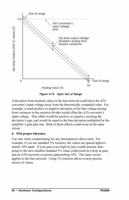
PK260056 s Hardware Configurations
Figure 4-15. Input Out of Range
A deviation from nominal values in the bias network could skew the A/Dconverters input voltage away from the theoretically computed value. Forexample, a small positive or negative deviation of the bias voltage arisingfrom variances in the resistive divider would offset the A/D convertersinput voltage. This offset would be positive or negative, tracking thedeviations sign, and would be equal to the bias deviation multiplied by theamplifiers gain plus one. Both of these effects could occur in the samecircuit.
6. Pick proper tolerance.
Use care when compensating for any discrepancies discovered. Forexample, if you use standard 5% resistors, the values are spaced approxi-mately 10% apart. If your gain is too high by just a small amount, thengoing to the next smallest standard 5% value could result in a drop in gain,and an A/D converter excursion approaching 10%. The same caveatapplies to the bias network. Using 1% resistors allows a more precisechoice of values.
0
10
2.5
Analog Input (V)
Op-
Am
p O
utpu
t (A
/D IC
Inpu
t) (
V)
A/D converter'sinput voltagelimit
Op-amp output voltagedeviation arising fromresistor variations
Out of range
Out of range
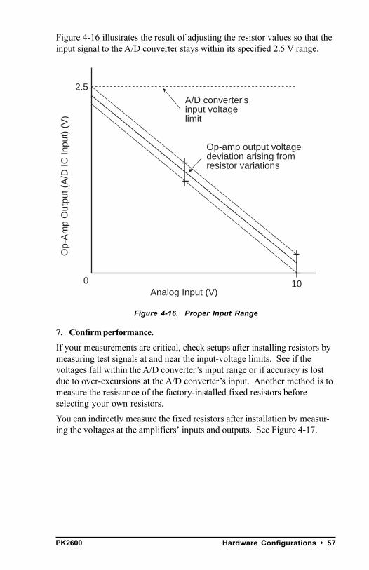
PK2600 Hardware Configurations s 57
Figure 4-16 illustrates the result of adjusting the resistor values so that theinput signal to the A/D converter stays within its specified 2.5 V range.
Figure 4-16. Proper Input Range
7. Confirm performance.
If your measurements are critical, check setups after installing resistors bymeasuring test signals at and near the input-voltage limits. See if thevoltages fall within the A/D converters input range or if accuracy is lostdue to over-excursions at the A/D converters input. Another method is tomeasure the resistance of the factory-installed fixed resistors beforeselecting your own resistors.
You can indirectly measure the fixed resistors after installation by measur-ing the voltages at the amplifiers inputs and outputs. See Figure 4-17.
0 10
2.5
Analog Input (V)
Op-
Am
p O
utpu
t (A
/D IC
Inpu
t) (
V)
A/D converter'sinput voltagelimit
Op-amp output voltagedeviation arising fromresistor variations
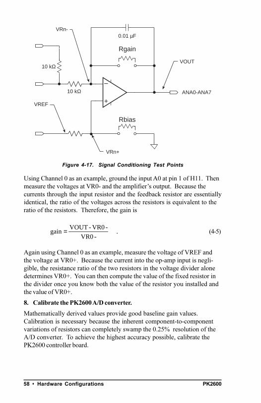
PK260058 s Hardware Configurations
Figure 4-17. Signal Conditioning Test Points
Using Channel 0 as an example, ground the input A0 at pin 1 of H11. Thenmeasure the voltages at VR0- and the amplifiers output. Because thecurrents through the input resistor and the feedback resistor are essentiallyidentical, the ratio of the voltages across the resistors is equivalent to theratio of the resistors. Therefore, the gain is
Again using Channel 0 as an example, measure the voltage of VREF andthe voltage at VR0+. Because the current into the op-amp input is negli-gible, the resistance ratio of the two resistors in the voltage divider alonedetermines VR0+. You can then compute the value of the fixed resistor inthe divider once you know both the value of the resistor you installed andthe value of VR0+.
8. Calibrate the PK2600 A/D converter.
Mathematically derived values provide good baseline gain values.Calibration is necessary because the inherent component-to-componentvariations of resistors can completely swamp the 0.25% resolution of theA/D converter. To achieve the highest accuracy possible, calibrate thePK2600 controller board.
ANA0-ANA7+
–
10 kΩ
10 kΩ
0.01 µF
Rgain
Rbias
VRn+
VRn-
VREF
VOUT
.-VR0
-VR0-VOUTgain = (4-5)

PK2600 Hardware Configurations s 59
Dynamic C provides a routine to compute calibration coefficients and storethe coefficients in nonvolatile memory. The routine uses two referencepoints to compute the coefficients. Each reference point comprises a pairof values: the actual applied test voltage and raw converted A/D value (a12-bit integer). The supplied Z-World A/D software will automatically usethese calibration coefficients to correct all subsequent A/D readings.
The factory installed fixed resistors have a 1% tolerance.
Calibration constants for the factory installed resistors are stored insimulated EEPROM during testing.
9. Recalibrate the PK2600.
To recalibrate a PK2600, apply two known test voltages to each channelyou plan to use. Get the converted reading for each test voltage and passthem, along with the test voltages, to the function eioBrdACalib tocalculate the conversion coefficients for that channel. eioBrdACalib willautomatically store the coefficients in the flash EPROM.
Sample program BL17AIN.C in the Dynamic C SAMPLES directory showshow to calibrate the conditioned analog input channels of a PK2600 manu-ally, assuming test voltages of 1.00 V and 9.00 V.
DriftThe AD680JT voltage reference displays a voltage drift of 10 ppm/°C (typ)to 30 ppm/°C (max). This drift corresponds to 25 mV/°C to 75 mV/°C, or1.75 mV to 5.25 mV over the temperature range of 0°C to 70°C.
The LMC660C operational amplifier exhibits an offset-voltage drift of 1.3 V/°C (typ), or 91 mV over the operating temperature range.
Low-Pass FilterThe 0.01 mF feedback capacitors in the amplifiers feedback path transformthe amplifiers into low-pass filters. These filters attenuate any high-frequency noise that may be present in your signal. These filters charac-teristics depend on the resistors your select.
The 3 dB corner frequency of a filter is
For the case above with a gain of 0.25 using a 1% feedback resistor of2490 Ω, the 3 dB corner frequency is 6392 Hz.
.F0.01R2
1f
gdb 3 µπ ××
= (4-6)
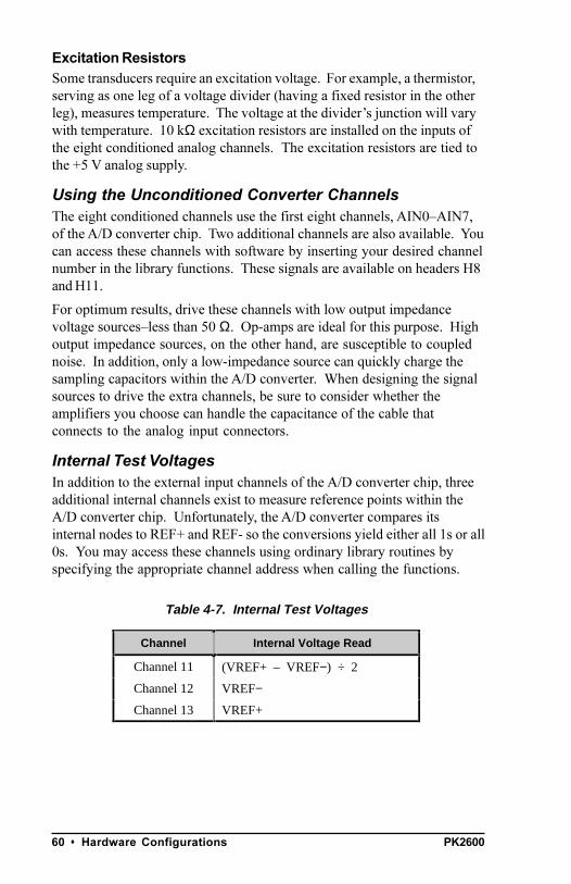
PK260060 s Hardware Configurations
Excitation ResistorsSome transducers require an excitation voltage. For example, a thermistor,serving as one leg of a voltage divider (having a fixed resistor in the otherleg), measures temperature. The voltage at the dividers junction will varywith temperature. 10 kΩ excitation resistors are installed on the inputs ofthe eight conditioned analog channels. The excitation resistors are tied tothe +5 V analog supply.
Using the Unconditioned Converter ChannelsThe eight conditioned channels use the first eight channels, AIN0AIN7,of the A/D converter chip. Two additional channels are also available. Youcan access these channels with software by inserting your desired channelnumber in the library functions. These signals are available on headers H8and H11.
For optimum results, drive these channels with low output impedancevoltage sourcesless than 50 Ω. Op-amps are ideal for this purpose. Highoutput impedance sources, on the other hand, are susceptible to couplednoise. In addition, only a low-impedance source can quickly charge thesampling capacitors within the A/D converter. When designing the signalsources to drive the extra channels, be sure to consider whether theamplifiers you choose can handle the capacitance of the cable thatconnects to the analog input connectors.
Internal Test VoltagesIn addition to the external input channels of the A/D converter chip, threeadditional internal channels exist to measure reference points within theA/D converter chip. Unfortunately, the A/D converter compares itsinternal nodes to REF+ and REF- so the conversions yield either all 1s or all0s. You may access these channels using ordinary library routines byspecifying the appropriate channel address when calling the functions.
Table 4-7. Internal Test Voltages
Channel Internal Voltage Read
Channel 11 (VREF+ – VREF−) ÷ 2
Channel 12 VREF−
Channel 13 VREF+

PK2600 Hardware Configurations s 61
Power-Down ModeIf you select Channel 14, the A/D converter chip enters a power-downmode in which all circuitry within the chip goes into a low-current, standbymode. Upon power-up and before the first conversion, the chip also goesinto the power-down mode. The chip remains in the power-down modeuntil you select a channel other than 14. The normal operating current ofthe A/D converter chip is 1 mA to 2.5 mA. In power-down mode thisconsumption is reduced to 4 µA to 25 µA.
External ConnectionsThe analog inputs on headers H8 and H11 are brought out to the PK2600ANALOG INPUTS DB25 connector throught the I/O conversion module.
PK260062 s Hardware Configurations
Serial ChannelsThere are four serial channels on the PK2600 controller board. One chan-nel, Channel 1, is a dedicated RS-232 communication channel, and is con-nected to the display board. Channel 0 is a dedicated RS-232 communica-tion channel. The remaining two channels may be either RS-232 or RS-485.
Channel 0 and Channel 1 are connected to the Z180s Serial Channel 0 andSerial Channel 1, respectively. Channel A and Channel B are controlled bythe Serial Communications Controller (SCC) chip on the controller board;these two ports also have hardware support for synchronous communica-tion. Serial channel signals are routed to either RS-232 or RS-485 convert-ers via configuration jumpers. Baud rates up to 57,600 bps are supported.
Table 4-8 summarizes the operating modes for the four channels.
Channel 0Channel 0 may be used as the controller boards RS-232 programming port,and is configured as three-wire or five-wire RS-232. Channel 0 cannot bereconfigured.
Channel AChannel A is a general-purpose serial channel controlled by a Zilog SerialCommunication Controller (SCC) chip on the controller board. Channel Acan be configured as two-wire RS-485 or five-wire RS-232. When config-ured as RS-232, Channel A also provides DCD and DTR signals. Synchro-nous communication is possible on this channel, but is not supported byDynamic C drivers at this time.
Channel BChannel B is a general-purpose serial channel. Along with Channel A, it iscontrolled by the Serial Communication Controller chip. Channel B can beconfigured as two-wire RS-485 or five-wire RS-232. Synchronous commu-nication is possible on this channel, but is not supported by Dynamic Cdrivers at this time.
Table 4-8. Serial Channel Configuration Options
Channel Configurations
Channel 0 Three-wire or five-wire RS-232 only
Channel 1 Three-wire RS-232 connection to display board
Channel A Two-wire RS-485 or five-wire RS-232, plus DCD andDTR
Channel B Two-wire RS-485 or five-wire RS-232
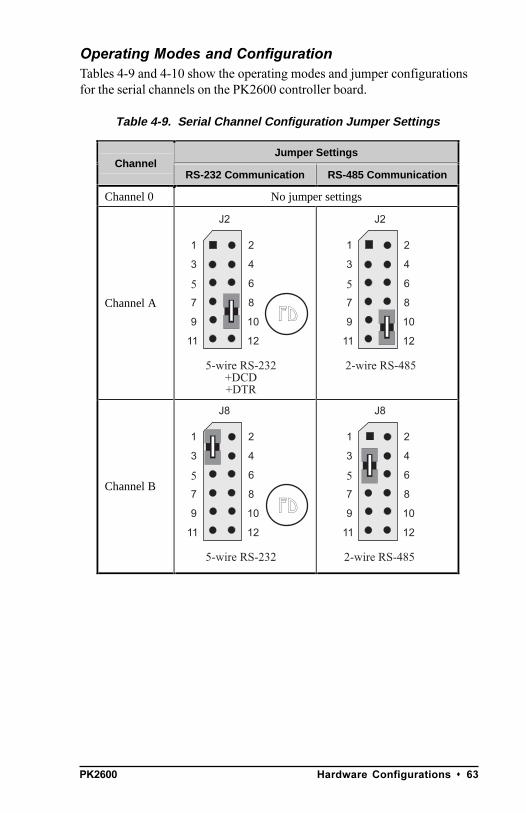
PK2600 Hardware Configurations s 63
Operating Modes and ConfigurationTables 4-9 and 4-10 show the operating modes and jumper configurationsfor the serial channels on the PK2600 controller board.
Table 4-9. Serial Channel Configuration Jumper Settings
Jumper SettingsChannel
RS-232 Communication RS-485 Communication
Channel 0 No jumper settings
Channel A
Channel B
10
12
J2
1 2
3 4
5 6
7 8
9
11
FD
5-wire RS-232+DCD+DTR
10
12
J8
1 2
3 4
5 6
7 8
9
11
FD
5-wire RS-232
10
12
J2
1 2
3 4
5 6
7 8
9
11
2-wire RS-485
10
12
J8
1 2
3 4
5 6
7 8
9
11
2-wire RS-485
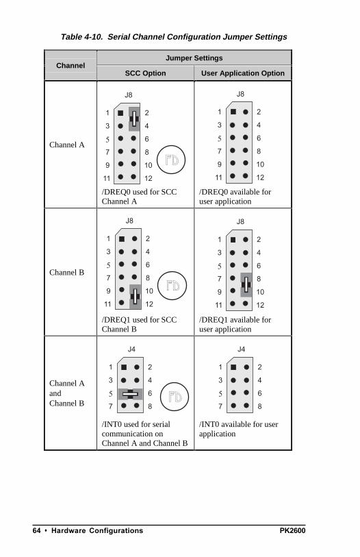
PK260064 s Hardware Configurations
Table 4-10. Serial Channel Configuration Jumper Settings
Jumper SettingsChannel
SCC Option User Application Option
Channel A
/DREQ0 used for SCCChannel A
/DREQ0 available foruser application
Channel B
/DREQ1 used for SCCChannel B
/DREQ1 available foruser application
Channel AandChannel B
/INT0 used for serialcommunication onChannel A and Channel B
/INT0 available for userapplication
10
12
J8
1 2
3 4
5 6
7 8
9
11
FD
10
12
J8
1 2
3 4
5 6
7 8
9
11
FD
J4
1 2
3 4
5 6
7 8FD
10
12
J8
1 2
3 4
5 6
7 8
9
11
10
12
J8
1 2
3 4
5 6
7 8
9
11
J4
1 2
3 4
5 6
7 8
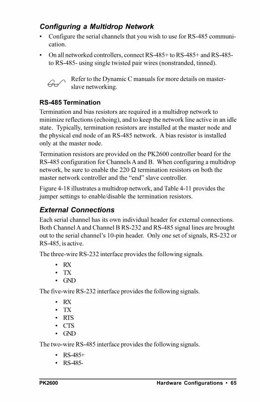
PK2600 Hardware Configurations s 65
Configuring a Multidrop Network Configure the serial channels that you wish to use for RS-485 communi-
cation.
On all networked controllers, connect RS-485+ to RS-485+ and RS-485-to RS-485- using single twisted pair wires (nonstranded, tinned).
Refer to the Dynamic C manuals for more details on master-slave networking.
RS-485 TerminationTermination and bias resistors are required in a multidrop network tominimize reflections (echoing), and to keep the network line active in an idlestate. Typically, termination resistors are installed at the master node andthe physical end node of an RS-485 network. A bias resistor is installedonly at the master node.
Termination resistors are provided on the PK2600 controller board for theRS-485 configuration for Channels A and B. When configuring a multidropnetwork, be sure to enable the 220 Ω termination resistors on both themaster network controller and the end slave controller.
Figure 4-18 illustrates a multidrop network, and Table 4-11 provides thejumper settings to enable/disable the termination resistors.
External ConnectionsEach serial channel has its own individual header for external connections.Both Channel A and Channel B RS-232 and RS-485 signal lines are broughtout to the serial channels 10-pin header. Only one set of signals, RS-232 orRS-485, is active.
The three-wire RS-232 interface provides the following signals.
RX TX GND
The five-wire RS-232 interface provides the following signals.
RX TX RTS CTS GND
The two-wire RS-485 interface provides the following signals.
RS-485+ RS-485-
$
PK260066 s Hardware Configurations
PK2600
Enable terminationresistors on themaster controllerand end controlleronly
PK2600
PK2600SERIAL PORT2/ 3
SERIAL PORT2/ 3
SERIAL PORT2/ 3
PK2600
SERIAL PORT2/ 3
Ground recommended
Figure 4-18. Multidrop Network
The RS-485 drivers supplied on the PK2600 controller boardsupport up to 32 nodes. The transmission bandwidth may bereduced as additional nodes over the benchmark quantity of32 are added to the network. Contact Z-World TechnicalSupport for assistance with large-scale network design.
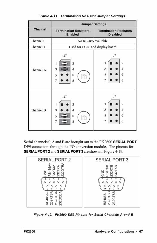
PK2600 Hardware Configurations s 67
Table 4-11. Termination Resistor Jumper Settings
Jumper Settings
Channel Termination ResistorsEnabled
Termination ResistorsDisabled
Channel 0 No RS-485 available
Channel 1 Used for LCD and display board
Channel A
Channel B
J7
1 2
3 4
5 6
7 8FD
J7
1 2
3 4
5 6
7 8FD
J7
1 2
3 4
5 6
7 8
J7
1 2
3 4
5 6
7 8
Serial channels 0, A and B are brought out to the PK2600 SERIAL PORTDE9 connectors through the I/O conversion module. The pinouts forSERIAL PORT 2 and SERIAL PORT 3 are shown in Figure 4-19.
Figure 4-19. PK2600 DE9 Pinouts for Serial Channels A and B
SERIAL PORT 3
GN
D
232R
XB
232T
XB
232C
TS
B23
2RT
SB
5 4 3 2 1
9 8 7 6
SERIAL PORT 2
GN
D
232R
XA
232T
XA
232C
TS
A23
2RT
SA
5 4 3 2 1
9 8 7 6
232D
TR
A23
2DC
DA
RS
485A
+R
S48
5A
RS
485B
+R
S48
5B
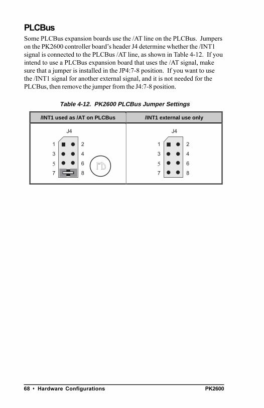
PK260068 s Hardware Configurations
Table 4-12. PK2600 PLCBus Jumper Settings
/INT1 used as /AT on PLCBus /INT1 external use only
J4
1 2
3 4
5 6
7 8FD
J4
1 2
3 4
5 6
7 8
PLCBusSome PLCBus expansion boards use the /AT line on the PLCBus. Jumperson the PK2600 controller boards header J4 determine whether the /INT1signal is connected to the PLCBus /AT line, as shown in Table 4-12. If youintend to use a PLCBus expansion board that uses the /AT signal, makesure that a jumper is installed in the JP4:7-8 position. If you want to usethe /INT1 signal for another external signal, and it is not needed for thePLCBus, then remove the jumper from the J4:7-8 position.
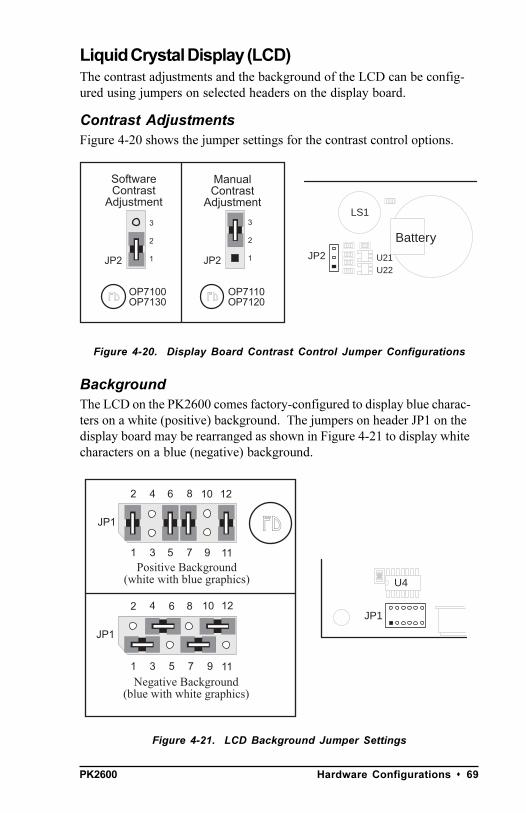
PK2600 Hardware Configurations s 69
JP2 JP2
SoftwareContrast
Adjustment
ManualContrast
Adjustment
FD FD OP7110OP7120
3
2
1
3
2
1
OP7100OP7130
U21U22
BatteryJP2
LS1
FD
Positive Background(white with blue graphics)
Negative Background(blue with white graphics)
JP1
U4
10 12
JP1
1
2
3
4
5
6
7
8
9 11
10 12
JP1
1
2
3
4
5
6
7
8
9 11
Liquid Crystal Display (LCD)The contrast adjustments and the background of the LCD can be config-ured using jumpers on selected headers on the display board.
Contrast AdjustmentsFigure 4-20 shows the jumper settings for the contrast control options.
Figure 4-20. Display Board Contrast Control Jumper Configurations
BackgroundThe LCD on the PK2600 comes factory-configured to display blue charac-ters on a white (positive) background. The jumpers on header JP1 on thedisplay board may be rearranged as shown in Figure 4-21 to display whitecharacters on a blue (negative) background.
Figure 4-21. LCD Background Jumper Settings

PK260070 s Hardware Configurations
Blank

PK2600 Subsystems s 71
CHAPTER 5: SUBSYSTEMS

PK260072 s Subsystems
Controller Board SubsystemsThe PK2600 controller board consists of several subsystems, including amicroprocessor core module, serial communications channels, digital I/O,analog inputs, and PLCBus expansion port. Figure 5-1 illustrates thesesubsystems.
Figure 5-1. Controller Board Block Diagram
Only the subsystems associated with the CM7200 core moduleare included in this chapter. See Chapter 4, Hardware Config-urations, for a description of the configurable subsystems.
Microprocessor Core ModuleThe controller board is built around a Z-World CM7200 Series microproces-sor core module. The core module consists of a Zilog Z180 microproces-sor, 32K of battery-backed static RAM, 128K of flash EPROM, a real-timeclock, and a watchdog timer/microprocessor supervisor.
The Z180 CPU runs at 18.432 MHz. Internal to the Z180 are two asynchro-nous serial ports, two DMA channels, two programmable-reload timers(PRTs), and three interrupt lines.
Six chip-select lines (/CS1/CS6) enable one of six groups of 64 I/Oaddresses. These lines are used to access peripherals on the controllerboard.
The power-supervisor IC performs several functions. It provides awatchdog timer function, performs power-failure detection, RAM protec-tion, and battery backup when the CM7200 is unpowered.
2
RS-232 or RS-485 (Ch A)
HVA[00–15]
Z180
PLCBus
Digital Inputs
K
CM7200
SCCRS-232 or RS-485 (Ch B)
HVB[00–15]
K
16
16
2803 Sinking Driver standard2985 Sourcing Driver optionalTTL or CMOS output optional
HVB[00–15]
GND
HVA[00–15]
GND
AIN[0–7]
ADREF
2543
ADCAIN[8–9]
Ref.
8
Input or outputbut not both
Input or outputbut not both
16
16
BatteryRAM
RTC
RS-232 (Ch 0)
Digital Outputs
Analog Inputs
LED 2.5 V
FlashEPROM
WatchdogSupervisor
+5 V
+5 V
Bank A
Bank B
RS-232 (Ch 1)to Display Board
$
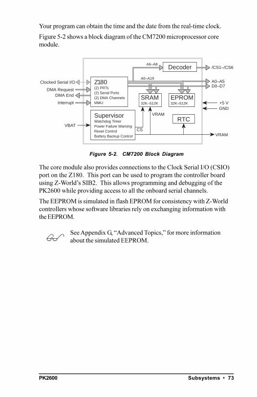
PK2600 Subsystems s 73
Your program can obtain the time and the date from the real-time clock.
Figure 5-2 shows a block diagram of the CM7200 microprocessor coremodule.
Figure 5-2. CM7200 Block Diagram
The core module also provides connections to the Clock Serial I/O (CSIO)port on the Z180. This port can be used to program the controller boardusing Z-Worlds SIB2. This allows programming and debugging of thePK2600 while providing access to all the onboard serial channels.
The EEPROM is simulated in flash EPROM for consistency with Z-Worldcontrollers whose software libraries rely on exchanging information withthe EEPROM.
See Appendix G, Advanced Topics, for more informationabout the simulated EEPROM.
DMA Request
A0–A5D0–D7
/CS1–/CS6
VBAT
GND
VRAM
Interrupt
A0–A19
A6–A8
CS
DMA End
Decoder
EPROM32K–512K
SRAM32K–512K
RTC
Z180(2) PRTs(2) Serial Ports(2) DMA ChannelsMMU
SupervisorWatchdog TimerPower Failure WarningReset ControlBattery Backup Control
VRAM
+5 V
Clocked Serial I/O
$

PK260074 s Subsystems
Flash2SRAM RTC
Batt.
Z180
Flash1
8
LCDControl VRAM2VRAM1
’691super.
KeypadInterface
EPLD
Backlight
RS-232Ch. 1
LCD320 x 240
8
Optional SoftwareContrast Adjustment
Contrast Adjustment
Drive
SenseBuzzer
Touchscreen
ToController
Board
!
Display Board SubsystemsThe PK2600 display board consists of several subsystems, including a com-puting module, serial communication channels, LCD, a buzzer, and a keypadinterface. Figure 5-3 provides a block diagram of the PK2600 display board.
Figure 5-3. Display Board Block Diagram
Computing ModuleThe computing module consists of a Zilog Z180 microprocessor, 128K ofbattery-backed static RAM, and 512K of flash EPROM. The computingmodule operates in tandem with a real-time clock and a watchdog timer/microprocessor supervisor.
The Z180 CPU runs at 18.432 MHz, and the LCD controller runs at9.216 MHz.
The watchdog timer/microprocessor chip provides a watchdog timerfunction, power-failure detection, RAM protection, and battery backup.
The real-time clock provides time and date information to applicationsrunning on the display board.
The EEPROM is simulated in flash EPROM for consistencywith Z-World controllers whose software libraries rely onexchanging information with the EEPROM. The simulatedEEPROM in the display board is unused at the present time,but addresses 0 and 1 are reserved for future use. Do not usethese addresses in your application.
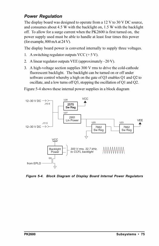
PK2600 Subsystems s 75
Power RegulationThe display board was designed to operate from a 12 V to 30 V DC source,and consumes about 4.5 W with the backlight on, 1.5 W with the backlightoff. To allow for a surge current when the PK2600 is first turned on, thepower supply used must be able to handle at least four times this power(for example, 800 mA at 24 V).
The display board power is converted internally to supply three voltages.
1. A switching regulator outputs VCC (+ 5 V).
2. A linear regulator outputs VEE (approximately 20 V).
3. A high-voltage section supplies 300 V rms to drive the cold-cathodefluorescent backlight. The backlight can be turned on or off undersoftware control whereby a high on the gate of Q3 enables Q1 and Q2 tooscillate, and a low turns off Q3, stopping the oscillation of Q1 and Q2.
Figure 5-4 shows these internal power supplies in a block diagram
Figure 5-4. Block Diagram of Display Board Internal Power Regulators
VCC
J10:91230 V DC
J11:5
1230 V DC
U28
2575Sw Reg
U27
2951Lin Power
U25
7662Sw Reg
U23
7662Sw Reg
VEE
VCC
2575Sw Reg
BacklightPower
from EPLD
300 V rms, 32.7 kHz,to CCFL backlight
Q3

PK260076 s Subsystems
Serial CommunicationThe display board has two serial channels that support asynchronouscommunication at baud rates from 300 bps to 57,600 bps. The serial chan-nels are factory-configured as two 3-wire RS-232 channels. Figure 5-5illustrates the configuration of these serial channels.
Figure 5-5. Display Board Serial Channels
Although the display board may be configured for RS-485serial communication, the factory-default RS-232 configurationis required for the connection to the controller board. Neitherthe second RS-232 channel nor the RS-485 channel is acces-sible when the display board is used with the PK2600.
Serial channel z1 of the display board is connected by a ribbon cable fromdisplay board header J8 to serial channel z1 on the controller boardthrough header H13 on the controller board.
T1OUTT2OUT
R1INR2IN
T1INT2INR1OUTR2OUT
TX1TXA0
232A
485TXA1
RX1RXA0
RXA1EN485
DRDERE
A
B
TXA0RTS0RXA0CTS0
U24
U26
to J8
!
PK2600 Subsystems s 77
691 Supervisor ChipBoth the display board and the controller board have an onboard 691supervisor. A voltage divider across the DC input provides a PFI signal tothe 691 watchdog supervisor. The 691 chip performs the followingservices.
Watchdog timer resets the microprocessor if software hangs.
Power-failure shutdown and reset.
Generates an early warning power-failure interrupt (PFI) that lets thesystem know when power is about to fail.
Memory protection feature prevents writes to RAM when power is low.
Supports battery backup.
Handling Power FluctuationsDuring a normal power-down, an interrupt service routine is used inresponse to a nonmaskable interrupt (NMI) to save vital state informationfor the application for when power recovers. The amount of code that theinterrupt service routine can execute depends on how fast the voltagedrops.
Theoretically, a power failure would cause a single NMI. Then, the inter-rupt service routine would restore data from the previous state when thevoltage recovers.
However, fluctuations in the DC input line could cause the 691 to see multi-ple crossings of the 1.3 V input power-reset threshold. These multiplenegative-edge transitions would, in turn, cause the Z180 to see multipleNMIs.
When the Z180 generates an NMI, it saves the program counter (PC) onthe processors stack. It next copies the maskable interrupt flag, IEF1, toIEF2 and zeroes IEF1. The Z180 will restore saved state information whenit executes a RETN (return from nonmaskable interrupt) instruction.
Ideally, the Z180 should be able to pop the stack and return to the locationwhere the program was first interrupted. But the original IEF1 flag is notrecoverable because the second and subsequent NMIs will have savedIEF1 = 0 to IEF2. Also, depending on the number of fluctuations of the DCinput (and hence, the number of stacked NMIs), the processors stack canoverflow, possibly into your programs code or data.

PK260078 s Subsystems
The following sample program shows how to handle an NMI.
main()...
...
char dummy[24];
...
#define NMI_BIT 0 ; bit 0
#JUMP_VEC NMI_VEC myint
#asmmyint::
ld sp,dummy+24 ; force stack pointer; to top of dummy vector; to prevent overwriting; code or data
do whatever service, within allowable execution time
loop:call hitwd ; make sure no watchdog reset
; while low voltageld bc,NMI ; load the read NMI register
; to bcin a,(c) ; read the read NMI register
; for /PFObit NMI_BIT, a ; check for status of /PFOjr z,loop ; wait until the brownout
; clearstimeout: ; then...a tight loop to
; force a watchdog timeout,jp timeout ; resetting the Z180
#endasm
Of course, if the DC input voltage continues to decrease, then the PK2600will just power down.
Call the Dynamic C function hitwd during the power-failure service routineto make sure that the watchdog timer does not time out and thereby resetthe processor. The controller can continue to run at low voltages, and so itmight not be able to detect the low-voltage condition after the watchdogtimer resets the processor.
Watchdog TimerTo increase reliability, the 691s watchdog timer forces a system reset if aprogram does not notify the supervisor nominally at least every second.

PK2600 Subsystems s 79
The assumption is that if the program fails to hit the watchdog, the programmust be stuck in a loop or halted. The Dynamic C function for hitting thewatchdog timer is hitwd. To hold the watchdog timer at bay, make a call tohitwd in a routine that runs periodically at the lowest software priority level.
A program can read the state of the WDO line with a call to wderror. Thismakes it possible to determine whether a watchdog timeout occurred. Thefollowing sample program shows how to do this when a program starts orrestarts.
main()if( wderror() ) wd_cleanup();hitwd();...
Power Shutdown and ResetWhen VCC (+5 V) drops below V
MIN (between 4.5 V and 4.75 V), the 691
supervisor asserts /RESET and holds it until VCC goes above VMIN
andstays that way for at least 50 ms. This delay allows the systems devices topower up and stabilize before the CPU starts.
PFI Early WarningWhen PFI drops below 1.3 V ± 0.05 V (i.e., DCIN drops below ~7.9 V for thecontroller board or ~10 V for the display board), the supervisor asserts /NMI (nonmaskable interrupt), and allows the program to clean up and getready for shutdown. The underlying assumption here is that PFI will causethe interrupt during a power failure before the 691 asserts /RESET.
Memory ProtectionWhen /RESET is active, the 691 supervisor disables the RAM chip-selectline, preventing accidental writes.
Battery BackupThe backup battery protects data in the RAM and the real-time clock (RTC).VRAM, the voltage supplied to the RAM and RTC, can also protect otherdevices attached to the system against power failures. The 691 supervisorswitches VRAM to VBAT or VCC, whichever is greater. (To prevent hunt-ing, the switchover actually occurs when Vcc is 50 mV higher than VBAT.)
The circuit draws no current from the battery once regular power is applied.
System ResetThe 691 chip drives the /RESET line. The /RESET line is not pulled upinternally.
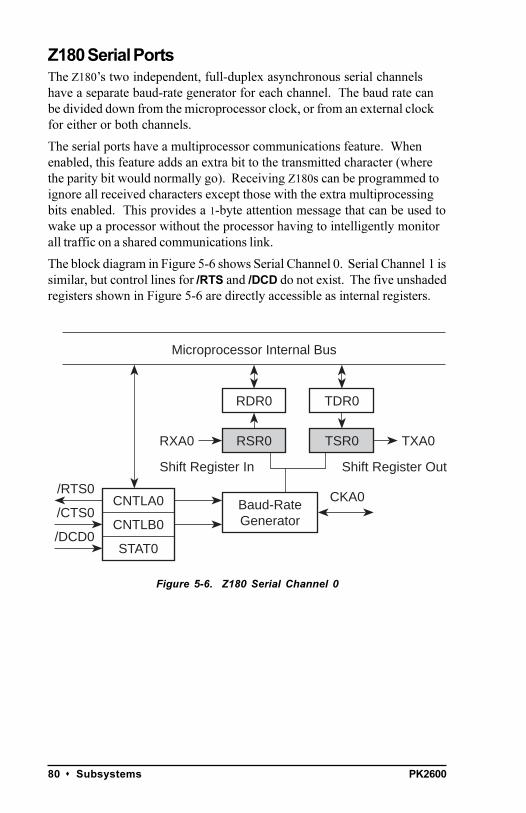
PK260080 s Subsystems
Z180 Serial PortsThe Z180s two independent, full-duplex asynchronous serial channelshave a separate baud-rate generator for each channel. The baud rate canbe divided down from the microprocessor clock, or from an external clockfor either or both channels.
The serial ports have a multiprocessor communications feature. Whenenabled, this feature adds an extra bit to the transmitted character (wherethe parity bit would normally go). Receiving Z180s can be programmed toignore all received characters except those with the extra multiprocessingbits enabled. This provides a 1-byte attention message that can be used towake up a processor without the processor having to intelligently monitorall traffic on a shared communications link.
The block diagram in Figure 5-6 shows Serial Channel 0. Serial Channel 1 issimilar, but control lines for /RTS and /DCD do not exist. The five unshadedregisters shown in Figure 5-6 are directly accessible as internal registers.
Figure 5-6. Z180 Serial Channel 0
Microprocessor Internal Bus
RDR0 TDR0
TSR0RXA0 TXA0
Shift Register OutShift Register In
Baud-RateGenerator
CKA0CNTLA0
STAT0
CNTLB0
/RTS0
/CTS0
/DCD0
RSR0
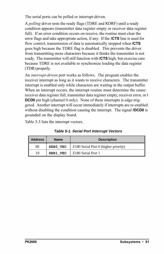
PK2600 Subsystems s 81
The serial ports can be polled or interrupt-driven.
A polling driver tests the ready flags (TDRE and RDRF) until a readycondition appears (transmitter data register empty or receiver data registerfull). If an error condition occurs on receive, the routine must clear theerror flags and take appropriate action, if any. If the /CTS line is used forflow control, transmission of data is automatically stopped when /CTSgoes high because the TDRE flag is disabled. This prevents the driverfrom transmitting more characters because it thinks the transmitter is notready. The transmitter will still function with /CTS high, but exercise carebecause TDRE is not available to synchronize loading the data register(TDR) properly.
An interrupt-driven port works as follows. The program enables thereceiver interrupt as long as it wants to receive characters. The transmitterinterrupt is enabled only while characters are waiting in the output buffer.When an interrupt occurs, the interrupt routine must determine the cause:receiver data register full, transmitter data register empty, receiver error, or /DCD0 pin high (channel 0 only). None of these interrupts is edge-trig-gered. Another interrupt will occur immediately if interrupts are re-enabledwithout disabling the condition causing the interrupt. The signal /DCD0 isgrounded on the display board.
Table 3-3 lists the interrupt vectors.
Table 5-1. Serial Port Interrupt Vectors
Address Name Description
0E SER0_VEC Z180 Serial Port 0 (higher priority)
10 SER1_VEC Z180 Serial Port 1
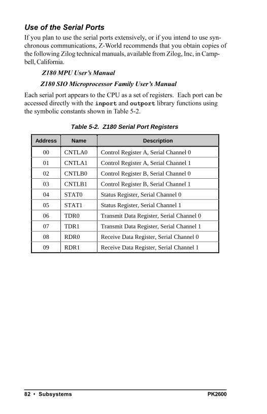
PK260082 s Subsystems
Use of the Serial PortsIf you plan to use the serial ports extensively, or if you intend to use syn-chronous communications, Z-World recommends that you obtain copies ofthe following Zilog technical manuals, available from Zilog, Inc, in Camp-bell, California.
Z180 MPU Users Manual
Z180 SIO Microprocessor Family Users Manual
Each serial port appears to the CPU as a set of registers. Each port can beaccessed directly with the inport and outport library functions usingthe symbolic constants shown in Table 5-2.
Table 5-2. Z180 Serial Port Registers
Address Name Description
00 CNTLA0 Control Register A, Serial Channel 0
01 CNTLA1 Control Register A, Serial Channel 1
02 CNTLB0 Control Register B, Serial Channel 0
03 CNTLB1 Control Register B, Serial Channel 1
04 STAT0 Status Register, Serial Channel 0
05 STAT1 Status Register, Serial Channel 1
06 TDR0 Transmit Data Register, Serial Channel 0
07 TDR1 Transmit Data Register, Serial Channel 1
08 RDR0 Receive Data Register, Serial Channel 0
09 RDR1 Receive Data Register, Serial Channel 1

PK2600 Subsystems s 83
Asynchronous Serial Communication InterfaceThe Z180 incorporates an asynchronous serial communication interface(ACSI) that supports two independent full-duplex channels.
ASCI Status RegistersA status register for each channel provides information about the state ofeach channel and allows interrupts to be enabled and disabled.
/DCD0 (Data Carrier Detect)This bit echoes the state of the /DCD0 input pin for Channel 0. However,when the input to the pin switches from high to low, the data bit switcheslow only after STAT0 has been read. The receiver is held to reset as longas the input pin is held high. This function is not generally useful becausean interrupt is requested as long as /DCD0 is a 1. This forces the program-mer to disable the receiver interrupts to avoid endless interrupts. A betterdesign would cause an interrupt only when the state of the pin changes.This pin is tied to ground in the CM7200.
TIE (Transmitter Interrupt Enable)This bit masks the transmitter interrupt. If set to 1, an interrupt is re-quested whenever TDRE is 1. The interrupt is not edge-triggered. Set thisbit to 0 to stop sending. Otherwise, interrupts will be requested continu-ously as soon as the transmitter data register is empty.
TDRE (Transmitter Data Register Empty)A 1 means that the channel is ready to accept another character. A highlevel on the /CTS pin forces this bit to 0 even though the transmitter isready.
STAT0 (04H)7 6 5 4 3 2 1 0
RDRF OVRN PE FE RIE /DCD0 TDRE TIE
R R R R R / W R R R / W
STAT1 (05H)7 6 5 4 3 2 1 0
RDRF OVRN PE FE RIE CTS1E TDRE TIE
R R R R R / W R R R / W
PK260084 s Subsystems
CTS1E (CTS Enable, Channel 1)The signals RXS and CTS1 are multiplexed on the same pin. A 1 stored inthis bit makes the pin serve the CTS1 function. A 0 selects the RXSfunction. (The pin RXS is the CSI/O data receive pin.) When RXS isselected, the CTS line has no effect.
RIE (Receiver Interrupt Enable)A 1 enables receiver interrupts and 0 disables them. A receiver interrupt isrequested under any of the following conditions: /DCD0 (Channel 0 only),RDRF (read data register full), OVRN (overrun), PE (parity error), and FE(framing error). The condition causing the interrupt must be removedbefore the interrupts are re-enabled, or another interrupt will occur. Read-ing the receiver data register (RDR) clears the RDRF flag. The EFR bit inCNTLA is used to clear the other error flags.
FE (Framing Error)A stop bit was missing, indicating scrambled data. This bit is cleared bythe EFR bit in CNTLA.
PE (Parity Error)Parity is tested only if MOD1 in CNTLA is set. This bit is cleared by theEFR bit in CNTLA.
OVRN (Overrun Error)Overrun occurs when bytes arrive faster than they can be read from thereceiver data register. The receiver shift register (RSR) and receiver dataregister (RDR) are both full. This bit is cleared by the EFR bit in CNTLA.
RDRF (Receiver Data Register Full)This bit is set when data is transferred from the receiver shift register to thereceiver data register. It is set even when one of the error flags is set, inwhich case defective data is still loaded to RDR. The bit is cleared whenthe receiver data register is read, when the /DCD0 input pin is high, and byRESET and IOSTOP.

PK2600 Subsystems s 85
ASCI Control Register AControl Register A affects various aspects of the asynchronous channeloperation.
MOD0MOD2 (Data Format Mode Bits)MOD0 controls stop bits: 0 ⇒ 1 stop bit, 1 ⇒ 2 stop bits. If 2 stop bits areexpected, then 2 stop bits must be supplied.
MOD1 controls parity: 0 ⇒ parity disabled, 1 ⇒ parity enabled. (See PEOin ASCI Control Register B for even/odd parity control.)
MOD2 controls data bits: 0 ⇒ 7 data bits, 1 ⇒ 8 data bits.
MPBR/EFR (Multiprocessor Bit Receive/Error Flag Reset)Reads and writes on this bit are unrelated. Storing a byte when this bit is 0clears all the error flags (OVRN, FE, PE). Reading this bit obtains the valueof the MPB bit for the last read operation when the multiprocessor mode isenabled.
/RTS0 (Request to Send, Channel 0)Store a 1 in this bit to set the RTS0 line from the Z180 high. This bit isessentially a 1-bit output port without other side effects.
CKA1D (CKA1 Disable)This bit controls the function assigned to the multiplexed pin (CKA1/~TEND0): 1 ⇒ ~TEND0 (a DMA function) and 0 ⇒ CKA1 (external clock I/O for Channel 1 serial port).
TE (Transmitter Enable)This bit controls the transmitter: 1 ⇒ transmitter enabled, 0 ⇒ transmitterdisabled. When this bit is cleared, the processor aborts the operation inprogress, but does not disturb TDR or TDRE.
CNTLA0 (00H)7 6 5 4 3 2 1 0
MPE RE TE /RTS0 MPBR/EFR
MOD2 MOD1 MOD0
R / W R / W R / W R / W R / W R / W R / W R / W
CNTLA1 (01H)7 6 5 4 3 2 1 0
MPE RE TE CKA1D MPBR/EFR
MOD2 MOD1 MOD0
R / W R / W R / W R / W R / W R / W R / W R / W
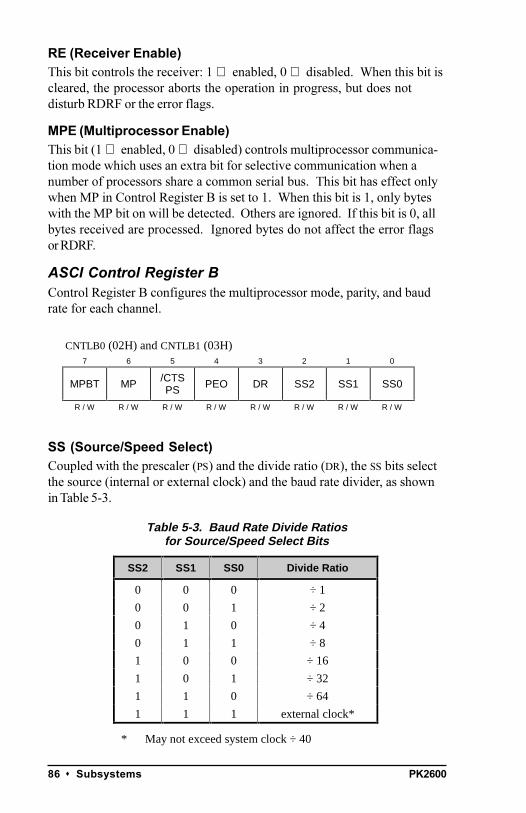
PK260086 s Subsystems
RE (Receiver Enable)This bit controls the receiver: 1 ⇒ enabled, 0 ⇒ disabled. When this bit iscleared, the processor aborts the operation in progress, but does notdisturb RDRF or the error flags.
MPE (Multiprocessor Enable)This bit (1 ⇒ enabled, 0 ⇒ disabled) controls multiprocessor communica-tion mode which uses an extra bit for selective communication when anumber of processors share a common serial bus. This bit has effect onlywhen MP in Control Register B is set to 1. When this bit is 1, only byteswith the MP bit on will be detected. Others are ignored. If this bit is 0, allbytes received are processed. Ignored bytes do not affect the error flagsor RDRF.
ASCI Control Register BControl Register B configures the multiprocessor mode, parity, and baudrate for each channel.
SS (Source/Speed Select)Coupled with the prescaler (PS) and the divide ratio (DR), the SS bits selectthe source (internal or external clock) and the baud rate divider, as shownin Table 5-3.
CNTLB0 (02H) and CNTLB1 (03H)7 6 5 4 3 2 1 0
MPBT MP /CTSPS PEO DR SS2 SS1 SS0
R / W R / W R / W R / W R / W R / W R / W R / W
Table 5-3. Baud Rate Divide Ratiosfor Source/Speed Select Bits
SS2 SS1 SS0 Divide Ratio
0 0 0 ÷ 1
0 0 1 ÷ 2
0 1 0 ÷ 4
0 1 1 ÷ 8
1 0 0 ÷ 16
1 0 1 ÷ 32
1 1 0 ÷ 64
1 1 1 external clock*
* May not exceed system clock ÷ 40
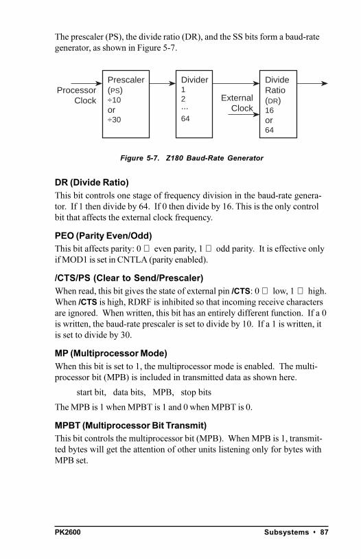
PK2600 Subsystems s 87
The prescaler (PS), the divide ratio (DR), and the SS bits form a baud-rategenerator, as shown in Figure 5-7.
Figure 5-7. Z180 Baud-Rate Generator
DR (Divide Ratio)This bit controls one stage of frequency division in the baud-rate genera-tor. If 1 then divide by 64. If 0 then divide by 16. This is the only controlbit that affects the external clock frequency.
PEO (Parity Even/Odd)This bit affects parity: 0 ⇒ even parity, 1 ⇒ odd parity. It is effective onlyif MOD1 is set in CNTLA (parity enabled).
/CTS/PS (Clear to Send/Prescaler)When read, this bit gives the state of external pin /CTS: 0 ⇒ low, 1 ⇒ high.When /CTS is high, RDRF is inhibited so that incoming receive charactersare ignored. When written, this bit has an entirely different function. If a 0is written, the baud-rate prescaler is set to divide by 10. If a 1 is written, itis set to divide by 30.
MP (Multiprocessor Mode)When this bit is set to 1, the multiprocessor mode is enabled. The multi-processor bit (MPB) is included in transmitted data as shown here.
start bit, data bits, MPB, stop bits
The MPB is 1 when MPBT is 1 and 0 when MPBT is 0.
MPBT (Multiprocessor Bit Transmit)This bit controls the multiprocessor bit (MPB). When MPB is 1, transmit-ted bytes will get the attention of other units listening only for bytes withMPB set.
Prescaler(PS)÷10or÷30
ProcessorClock
Divider12...64
DivideRatio(DR)16or64
ExternalClock

PK260088 s Subsystems
Table 5-4 relates the Z180s ASCI Control Register B to the baud rate.
Table 5-4. Baud Rates for ASCI Control Register B
ASCIB Value
Baud Rate at9.216 MHz
(bps)
Baud Rate at18.432 MHz
(bps)
ASCIB Value
Baud Rate at9.216 MHz
(bps)
Baud Rate at18.432 MHz
(bps)
00 57,600 115,200 20 19,200 38,400
01 28,800 57,600 21 9600 19,200
02 or 08 14,400 28,800 22 or 28 4800 9600
03 or 09 7200 14,400 23 or 29 2400 4800
04 or 0A 3600 7200 24 or 2A 1200 2400
05 or 0B 1800 3600 25 or 2B 600 1200
06 or 0C 900 1800 26 or 2C 300 600
0D 450 900 2D 150 300
0E 225 450 2E 75 150

PK2600 Software Development s 89
CHAPTER 6:
SOFTWARE DEVELOPMENT
Chapter 6 describes the software function calls used to develop applica-tions with the PK2600. The following major sections are included.
Supplied Software
Digital I/O
Analog Inputs
Serial Channels
Display Board Functions
Additional Software

PK260090 s Software Development
Supplied SoftwareSoftware drivers for controlling the PK2600s inputs/outputs and serialports are provided with Dynamic C. In order to use these drivers, it isnecessary to include the appropriate Dynamic C libraries. These librariesare listed in Table 6-1.
Your application program can use these libraries by including them in yourprogram. To include these libraries, use the #use directive as shown below.
#use drivers.lib
Since the controller and the display boards are programmedseparately, remember to #use the corresponding libraries fromTable 6-1, depending on which board is being programmed.
The SIB2 is needed to program the display board.
See the Dynamic C Technical Reference manual for moreinformation on #use and other libraries.
Table 6-1. PK2600 Software Libraries
Library Description
General Libraries
AASC.LIB All serial communication applications
DRIVERS.LIB General drivers
SYS.LIB General drivers
Controller Board Libraries
AASCURT2.LIB XP8700 applications only
EZIOBL17.LIB All controller board applications
EZIOPBDV.LIB All expansion board applications
EZIOPLC2.LIB All expansion board applications
Display Board Libraries
EZIOOP71.LIB All OP7100 applications
GLCD.LIB LCD applications
KP_OP71.LIB Touchscreen read applications
LQVGA.LIB Landscape image VGA drivers
PQVGA.LIB Portrait image VGA drivers
!
!
$
PK2600 Software Development s 91
Digital I/O
Digital InputsThe PK2600 controller board is equipped with protected digital inputsdesigned as logical data inputs that return a 1 when the input is high or 0when the input is low.
A low-pass filter on each input channel has a time constant of:
TRC
= 220 µs (4.5 kHz).
If the signals present on the digital inputs change states faster than this,the readings on the inputs may not be accurate.
How to Read the InputThis section provides information on using the Dynamic C software driversfor the controller boards protected digital inputs.
The following software drivers read the status of the protected digitalinputs.
unsigned BankA( unsigned eioAddr )
unsigned BankB( unsigned eioAddr )
BankA converts eioAddr to a value of 1631 for addressing thecorrect input or output assignments. BankB converts eioAddr to avalue of 015.
PARAMETER: eioAddr specifies channel number from 015.
RETURN VALUE: the formatted I/O assignment, or 1 if the parametereioAddr is out of range.
int eioBrdDI( unsigned eioAddr )
Reads the state from one of the 32 physical digital inputs. SetseioErrorCode if eioAddr is out of range.
PARAMETER: eioAddr specifies the input to be read. Valid numbersare from 0 to 31. 015 represents Bank B. 1631 represents Bank A.
RETURN VALUE: 0 if input reads low, 1 if input reads high.
unsigned inport( unsigned port )
Reads a value from an I/O port.
PARAMETER 1: port is the PK2600 controller board port address toread. When used to read the digital inputs, port is one of four groupsof eight inputs. There are two groups of eight inputs for each bank.
RETURN VALUE: The value read from the port.
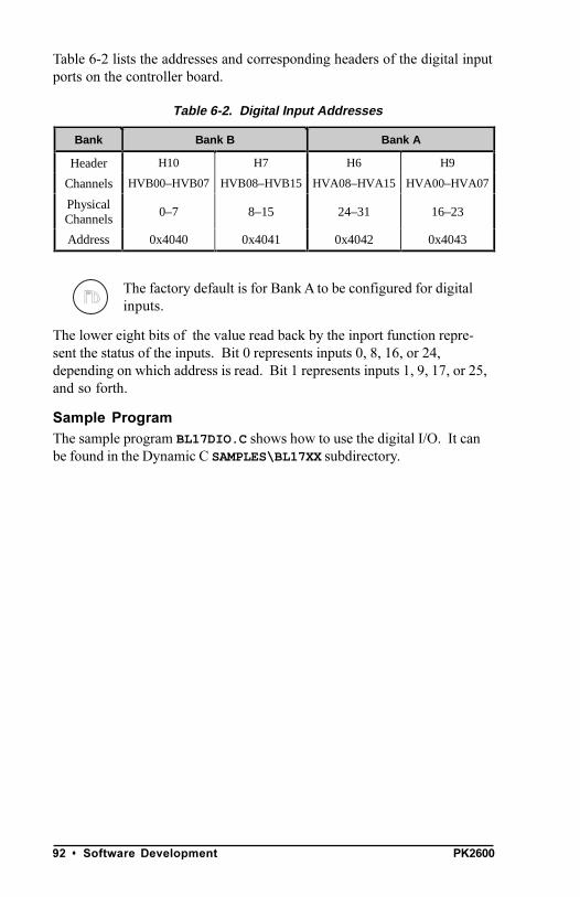
PK260092 s Software Development
Table 6-2 lists the addresses and corresponding headers of the digital inputports on the controller board.
The factory default is for Bank A to be configured for digitalinputs.
The lower eight bits of the value read back by the inport function repre-sent the status of the inputs. Bit 0 represents inputs 0, 8, 16, or 24,depending on which address is read. Bit 1 represents inputs 1, 9, 17, or 25,and so forth.
Sample ProgramThe sample program BL17DIO.C shows how to use the digital I/O. It canbe found in the Dynamic C SAMPLES\BL17XX subdirectory.
Table 6-2. Digital Input Addresses
Bank Bank B Bank A
Header H10 H7 H6 H9
Channels HVB00–HVB07 HVB08–HVB15 HVA08–HVA15 HVA00–HVA07
PhysicalChannels
0–7 8–15 24–31 16–23
Address 0x4040 0x4041 0x4042 0x4043
FD

PK2600 Software Development s 93
Digital OutputsThe PK2600 controller board provides up to 32 high-voltage, high-currentdriver outputs. Some outputs can also function as pulse width modulated(PWM) outputs. This section provides information on the Dynamic Csoftware drivers for the controller boards high-voltage driver outputs.
The following software function turns a specified high-voltage driver ONor OFF.
unsigned BankA( unsigned eioAddr )
unsigned BankB( unsigned eioAddr )
BankA converts eioAddr to a value of 1631 for addressing the correctinput or output assignments. BankB converts eioAddr to a value of015.
PARAMETER: eioAddr specifies channel number from 015.
RETURN VALUE: the formatted I/O assignment, or -1 if the parametereioAddr is out of range.
int eioBrdDO( unsigned eioAddr, char state )
Sets the state of a digital output. Sets eioErrorCode if parametereioAddr is out of range.
PARAMETERS: eioAddr specifies the output to be set. Validnumbers are from 0 to 31. 015 represents Bank B. 1631 representsBank A.
state is the desired output state for the specified output. A non-zerovalue turns the output on. A zero turns the output off.
RETURN VALUE: Returns 0 if successful, -1 if eioAddr is out ofrange.
void outport( unsigned port, unsigned value )
Writes data to an I/O port.
PARAMETERS: port is the PK2600 controller board port address tobe written. When used to write to the digital outputs, port is one offour groups of eight outputs. There are two groups of eight outputsfor each bank.
value is the data to be written to the port. When used to write to thedigital outputs, data bits D3, D2, and D1 determine which output in agroup is selected. Data bit D0 determines the state of the output. Databits D7 through D4 are unused.
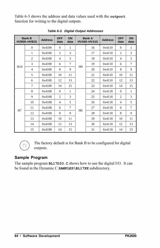
PK260094 s Software Development
Table 6-3 shows the address and data values used with the outportfunction for writing to the digital outputs.
The factory default is for Bank B to be configured for digitaloutputs.
Sample ProgramThe sample program BL17DIO.C shows how to use the digital I/O. It canbe found in the Dynamic C SAMPLES\BL17XX subdirectory.
Table 6-3. Digital Output Addresses
Bank BHVB00–HVB15 Address OFF
dataON
dataBank A
HVA00–HVA15 Address OFFdata
ONdata
0 0x4100 0 1 16 0x4110 0 1
1 0x4100 2 3 17 0x4110 2 3
2 0x4100 4 5 18 0x4110 4 5
3 0x4100 6 7 19 0x4110 6 7
4 0x4100 8 9 20 0x4110 8 9
5 0x4100 10 11 21 0x4110 10 11
6 0x4100 12 13 22 0x4110 12 13
H10
7 0x4100 14 15
H9
23 0x4110 14 15
8 0x4108 0 1 24 0x4118 0 1
9 0x4108 2 3 25 0x4118 2 3
10 0x4108 4 5 26 0x4118 4 5
11 0x4108 6 7 27 0x4118 6 7
12 0x4108 8 9 28 0x4118 8 9
13 0x4108 10 11 29 0x4118 10 11
14 0x4108 12 13 30 0x4118 12 13
H7
15 0x4108 14 15
H6
31 0x4118 14 15
FD
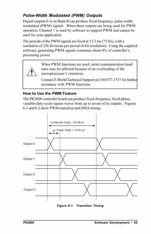
PK2600 Software Development s 95
Pulse-Width Modulated (PWM) OutputsDigital outputs 06 on Bank B can produce fixed-frequency, pulse-widthmodulated (PWM) signals. When these outputs are being used for PWMoperation, Channel 7 is used by software to support PWM and cannot beused for your application.
The periods of the PWM signals are fixed at 13.3 ms (75 Hz), with aresolution of 256 divisions per period (8-bit resolution). Using the suppliedsoftware, generating PWM signals consumes about 8% of controllersprocessing power.
When PWM functions are used, serial communication baudrates may be affected because of an overloading of themicroprocessors resources.
Contact Z-World Technical Support at (530)757-3737 for furtherassistance with PWM functions.
How to Use the PWM FeatureThe PK2600 controller board can produce fixed-frequency, fixed-phase,variable-duty-cycle square waves from up to seven of its outputs. Figures6-1 and 6-2 show PWM transition and DMA timing.
Figure 6-1. Transition Timing
Composite Edge = 52.08 µs
Single Edge = 13.02 µs
Output 0
Output 1
Output 3
Output 2
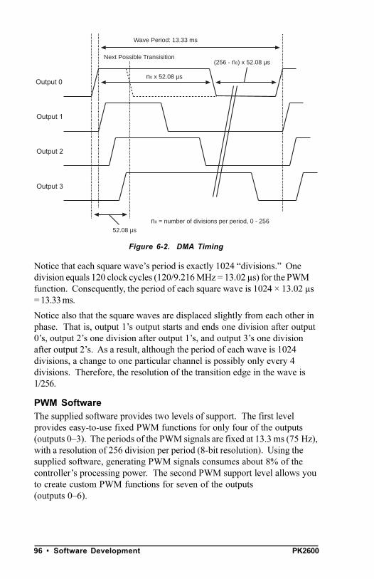
PK260096 s Software Development
Figure 6-2. DMA Timing
Notice that each square waves period is exactly 1024 divisions. Onedivision equals 120 clock cycles (120/9.216 MHz = 13.02 µs) for the PWMfunction. Consequently, the period of each square wave is 1024 × 13.02 µs= 13.33 ms.
Notice also that the square waves are displaced slightly from each other inphase. That is, output 1s output starts and ends one division after output0s, output 2s one division after output 1s, and output 3s one divisionafter output 2s. As a result, although the period of each wave is 1024divisions, a change to one particular channel is possibly only every 4divisions. Therefore, the resolution of the transition edge in the wave is1/256.
PWM SoftwareThe supplied software provides two levels of support. The first levelprovides easy-to-use fixed PWM functions for only four of the outputs(outputs 03). The periods of the PWM signals are fixed at 13.3 ms (75 Hz),with a resolution of 256 division per period (8-bit resolution). Using thesupplied software, generating PWM signals consumes about 8% of thecontrollers processing power. The second PWM support level allows youto create custom PWM functions for seven of the outputs(outputs 06).
Wave Period: 13.33 ms
Next Possible Transisition
n0 x 52.08 µs
(256 - n0) x 52.08 µs
52.08 µs
Output 2
Output 0
Output 1
Output 3
n0 = number of divisions per period, 0 - 256

PK2600 Software Development s 97
The following three functions are the first level functions. They aredesigned for ease of use. These functions are located in EZIODPWM.LIBthat is automatically included when EZIOBL17.LIB is included.
int eioBrdAO( unsigned eioAddr, unsigned state )
Specifies the duty cycle for a particular output channel. SeteioErrorCode if eioAddr is out of range.
PARAMETERS: eioAddr is a number ranging from 0 to 3.
state is a placeholder for a number ranging from 0 (to turn off thechannel) to 256 (to turn-on the channel, 100% duty cycle). The dutycycle is state/256 (e.g., 128 for 50% duty cycle, 64 for 25% duty cycle).
RETURN VALUE: 0 if successful, 1 if not.
The PWM functions use the Z180s built-in DMA hardware.The use of DMA-driven PWM effectively makes the Z180 runat least 8% more slowly.
Be sure your application calls _eioBrdAORf at least every25 ms to refresh the drivers period.
Contact Z-World Technical Support at (530)757-3737 for furtherassistance with PWM functions.
void _eioSetupAO1st ()
Initializes the PWM hardware.
_eioSetupAO1st must be called before using eioBrdAO.
int _eioBrdAORf ()
Refreshes the DMA counter and address pointer.
Your program must call it every 25 ms (or more frequently) after_eioSetupAO1st is called.
RETURN VALUE: The function returns -1 if the DMA count is zero(PWM has stopped), and returns 0 otherwise. If the function returns -1,the driver is either not initialized (by calling _eioSetupAO1st), or_eioBrdAORf is not called at least every 25 ms.
Sample ProgramBL17PWM4.C is a sample program that shows how to use the pulse widthmodulation feature using the functions listed above. It can be found in theDynamic C directory under SAMPLES\BL17XX.
PK260098 s Software Development
Analog InputsThe PK2600s analog inputs provide an easy-to-use interface to a widevariety of sensors and transducers. The PK2600 provides 10 single-endedA/D conversion channels with 12-bit resolution.
Using the Analog InputsThe factory calibrates each PK2600, storing each units individual zerooffset and actual gain for its eight primary channels in simulated EEPROM.Your application can use library functions to access the simulatedEEPROMs calibration constants to correct measurements for offset andgain error.
void eioBrdInit( int flags )
Initializes the analog-to-digital converter to the default output mode.The default mode is unipolar input, 12-bit data length, most significantbit first.
PARAMETER: flags is not used at this level and should be set to 0.
Call eioBrdInit before calling eioBrdAI.
int eioBrdAI( unsigned eioAddr )
Reads one of the 10 voltage inputs and performs analog-to-digitalconversion. Sets eioErrorCode if eioAddr is out of range.
PARAMETER: eioAddr specifies an input number of 0 to 9 or 16 to 25to be read. eioAddr values 0 through 9 represent analog inputs 0through 9, and will cause the function to return the voltage read on aninput. eioAddr values 16 through 25 also represent analog inputs 0through 9, but cause the function to return a 12-bit raw data value forthe analog input.
RETURN VALUE: The function returns the voltage read as a realnumber in a floating-point representation for eioAddr values 09 if theread is successful. For eioAddr values 1625, if the read is successful,the function returns a floating-point representation of an unsignedinteger value (04095) for the 12-bit raw data value read from the A/Dconverter.
int eioBrdAdcMode( int datalen, int dataformat,int polarformat )
Sets the analog-to-digital conversion data length, data format, andpolarity format other than default. Call this function after eioBrdInitand before eioBrdAI.
RETURN VALUE: returns 1 if successful, -1 if an invalid parameter ispassed to the function.
!

PK2600 Software Development s 99
Call eioBrdAdcMode after calling eioBrdInit and beforecalling eioBrdAI.
Table 6-4 shows the parameters datalen, dataformat, and polarformat.
int eioBrdACalib( int eioAddr, unsigned d1,unsigned d2, float v1, float v2 )
Calculates the calibration constants for an analog input channel usingtwo known voltages and two corresponding raw data readings. Storesthe calibration constants in EEPROM.
PARAMETERS: eioAddr is the analog input channel.
d1 is the raw data corresponding to v1.
d2 is the raw data corresponding to v2.
v1 is the known voltage used to obtain d1.
v2 is the known voltage used to obtain d2.
RETURN VALUE: 0 if successful, 1 if eioAddr is out of range.
Since the PK2600 is calibrated at the factory, it is only neces-sary to use this function to recalibrate the PK2600 controllerboard.
Sample ProgramBL17AIN.C is a sample program that shows how to use the analog inputs.It can be found in the Dynamic C directory under SAMPLES\BL17XX.
Table 6-4. Analog-to-Digital Converter Modes
Parameter Value
datalen 0 – 12-bit data length1 – 8-bit data length2 – 12-bit data length3 – 16-bit data length
dataformat 0 – most significant bit first1 – least significant bit first
polarformat 0 – unipolar1 – bipolar
!
!
PK2600100 s Software Development
Serial ChannelsThe PK2600 provides three serial communication channels. Two ports canbe configured as RS-232 or RS-485; the remaining port, SERIAL PORT 1, isRS-232 only. This section provides information on RS-232 and RS-485communications.
Chapter 4, Hardware Configurations, provides informationon configuring the serial channels.
RS-232 CommunicationThe RS-232 channels and the supplied Dynamic C software allow thePK2600 to communicate with other computers or controllers. By adding amodem, remote communications can be achieved (including remote down-loading) using the X-modem protocol. Examples of RS-232 software driverscan be found in the Dynamic C \SAMPLES\AASC directory.
Refer to your Dynamic C manuals for additional information onremote downloading.
Use the SIB2 if you need to make all the serial channelsavailable to your application during software development.See Chapter 2, Getting Started, and Appendix D, SerialInterface Board 2, for more information.
RS-485 CommunicationThe PK2600 controller board can be configured to provide up to threechannels of RS-485 communications. RS-485 is an asynchronous multidrophalf-duplex standard that provides multidrop networking with maximumcable lengths up to 4000 feet.
Dynamic C provides library functions for master-slave two-wire half-duplexRS-485 9th-bit binary communications.
This RS-485 hardware standard supports up to 32 controllers on onenetwork. The supplied software supports 1 master unit, plus up to 255slave units (which may consist of any combination of Z-World controllersthat support the RS-485 protocol).
$
$
Tip
PK2600 Software Development s 101
SoftwareSerial channel 0 is supported by Dynamic C library functions.
Serial channels A and B are driven by U13 (a Zilog Serial CommunicationController) on the controller board. Serial channels A and B have addi-tional capabilities beyond those supported by the Dynamic C libraries. Ifyou would like to use these additional capabilities, refer to the Zilog SerialCommunication Controllers Manual.
Comprehensive information on the serial channel software andprogramming can be found in the Dynamic C FunctionReference manual and the Dynamic C Application Frame-works manual.
The following functions are used with the RS-485 serial channels.
int sccSw485( unsigned channel, unsigned state )
Enables or disables the RS-485 drivers for Channel A or Channel B onthe SCC.
PARAMETERS: channel is SCC_A or SCC_B.
state is 1 to enable the driver, 0 to disable it.
RETURN VALUE: 0 if channel is valid, -1 if not.
int z1Sw485( unsigned state )
Enables or disables the RS-485 driver for Channel 1.
PARAMETER: state is 1 to enable the driver, 0 to disable it.
RETURN VALUE: 0 if channel is valid.
Sample ProgramBL17SCC.C is a serial communication sample program found in theDynamic C SAMPLES\BL17XX directory.
$
PK2600102 s Software Development
Display Board Functions
Display Hardware ControlThe following functions from the Dynamic C EZIOOP71.LIB library areused to control the hardware aspects of the display, including the back-light, the contrast, and the beeper.
void op71BackLight( int onOff )
Turns the backlight of the PK2600 on or off.
PARAMETER: onOff is non-zero to turn the backlight on, zero to turnthe backlight off.
void op71SetContrast( unsigned contrast )
Controls the contrast of the LCD.
PARAMETER: contrast values range from 0 to 127, 0 for the leastcontrast (minimum VEE), 127 for the most contrast (maximum VEE).
void eioBeep( int onOff )
Turns the buzzer on or off.
PARAMETER: onOff is non-zero to turn the buzzer on, zero to turnthe buzzer off.
Display ImagesThe following functions from the Dynamic C GLCD.LIB library are used tocontrol the appearance of the fonts, lines, and bitmaps on the LCD.
void glFontInit( struct _fontInfo *pInfo,char pixWidth, char pixHeight,unsigned startChar, unsigned endChar,char *bitmapBuffer )
Initializes a font descriptor with the bitmap defined in the root memory.For fonts with bitmaps defined in xmem, use glXFontInit.
PARAMETERS: pInfo is a pointer to the font descriptor to be initialized.
pixWidth is the width of each font item (pixWidth must be uniformfor all items).
pixHeight is the height of each font item (pixHeight must beuniform for all items).
startChar is the offset to the first useable item (useful for fonts forASCII or other fonts with an offset).
endChar is the index of the last useable font item.
bitmapBuffer is a pointer to a linear array of the font bitmap. Thebitmap is a column with the major byte aligned.
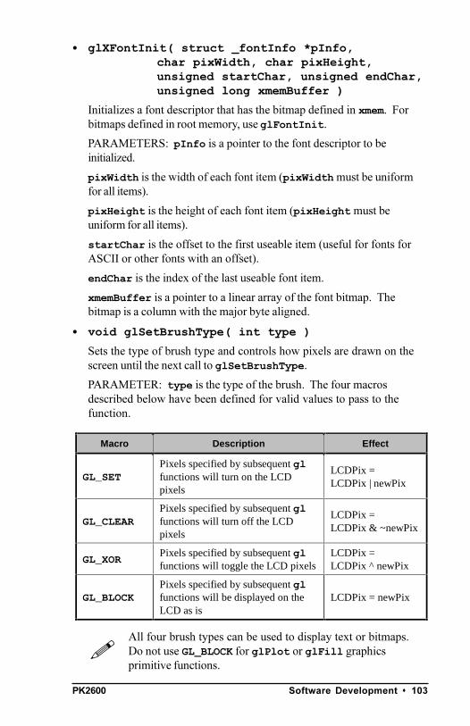
PK2600 Software Development s 103
glXFontInit( struct _fontInfo *pInfo,char pixWidth, char pixHeight,unsigned startChar, unsigned endChar,unsigned long xmemBuffer )
Initializes a font descriptor that has the bitmap defined in xmem. Forbitmaps defined in root memory, use glFontInit.
PARAMETERS: pInfo is a pointer to the font descriptor to beinitialized.
pixWidth is the width of each font item (pixWidth must be uniformfor all items).
pixHeight is the height of each font item (pixHeight must beuniform for all items).
startChar is the offset to the first useable item (useful for fonts forASCII or other fonts with an offset).
endChar is the index of the last useable font item.
xmemBuffer is a pointer to a linear array of the font bitmap. Thebitmap is a column with the major byte aligned.
void glSetBrushType( int type )
Sets the type of brush type and controls how pixels are drawn on thescreen until the next call to glSetBrushType.
PARAMETER: type is the type of the brush. The four macrosdescribed below have been defined for valid values to pass to thefunction.
All four brush types can be used to display text or bitmaps.Do not use GL_BLOCK for glPlot or glFill graphicsprimitive functions.
Macro Description Effect
GL_SETPixels specified by subsequent glfunctions will turn on the LCDpixels
LCDPix =LCDPix | newPix
GL_CLEARPixels specified by subsequent glfunctions will turn off the LCDpixels
LCDPix =LCDPix & ~newPix
GL_XORPixels specified by subsequent glfunctions will toggle the LCD pixels
LCDPix =LCDPix ^ newPix
GL_BLOCKPixels specified by subsequent glfunctions will be displayed on theLCD as is
LCDPix = newPix
!

PK2600104 s Software Development
int glInit()
Initializes the LCD module (software and hardware).
RETURN VALUE: the status of the LCD. If the initialization wassuccessful, this function returns 0. Otherwise, the returned valueindicates the LCD status.
int glPlotDot( int x, int y )
Plots one pixel on the screen at coordinate (x,y).
PARAMETERS: x is the x coordinate of the pixel to be drawn.
y is the y coordinate of the pixel to be drawn.
RETURN VALUE: Status of the LCD after the operation.
void glPlotLine( int x1, int y1, int x2, int y2 )
Plots a line on the LCD.
PARAMETERS: x1 is the x coordinate of the first endpoint.
y1 is the y coordinate of the first endpoint.
x2 is the x coordinate of the second endpoint.
y2 is the y coordinate of the second endpoint.
void glPrintf( int x, int y,struct _fontInfo *pInfo, char *fmt,... )
Prints a formatted string (much like printf) on the LCD screen.
PARAMETERS: x is the x coordinate of the text (left edge).
y is the y coordinate of the text (top-edge).
*pInfo is the pointer to the font descriptor used for printing on theLCD screen.
*fmt is the pointer to the format string
void glPlotCircle( int xc, int yc, int rad )
Draws a circle on the LCD.
PARAMETERS: xc is the x coordinate of the center.
yc is the y coordinate of the center.
rad is the radius of the circle.
void glFillCircle( int xc, int yc, int rad )
Draws a filled-in circle on the LCD.
PARAMETERS: xc is the x coordinate of the center.
yc is the y coordinate of the center.
rad is the radius of the circle.

PK2600 Software Development s 105
void glPlotVPolygon( int n, int *pFirstCoord )
Plots a filled-in polygon.
PARAMETERS: n is the number of vertices.
*pFirstCoord is an array of vertex coordinates (x1,y
1), (x
2,y
2),
void glPlotPolygon( int n, int x1, int y1, int x2, int y2,... )
Plots the outline of a polygon.
PARAMETERS: n is the number of vertices.
x1 is the x coordinate of the first vertex.
y1 is the y coordinate of the first vertex.
x2 is the x coordinate of the second vertex.
y2 is the y coordinate of the second vertex.
void glFillVPolygon( int n, int *pFirstCoord )
Fills in a polygon.
PARAMETERS: n is the number of vertices.
*pFirstCoord is an array of vertex coordinates (x1,y
1), (x
2,y
2),
void glFillPolygon( int n, int x1, int y1, int x2, int y2,... )
Fllls in a polygon.
PARAMETERS: n is the number of vertices.
x1 is the x coordinate of the first vertex.
y1 is the y coordinate of the first vertex.
x2 is the x coordinate of the second vertex.
y2 is the y coordinate of the second vertex.
void glPutBitmap( int x, int y, int bmWidth,int bmHeight, char *bm )
Displays a bitmap stored in root memory on the LCD. For bitmapsdefined in xmem memory, use glXPutBitmap.
PARAMETERS: x is the x coordinate of the bitmap left edge.
y is the y coordinate of the bitmap top edge.
bmWidth is the width of the bitmap.
bmHeight is the height of the bitmap.
bm is a pointer to the bitmap. The bitmap format is a column with themajor byte aligned for each column.

PK2600106 s Software Development
void glXPutBitmap( int x, int y, int bmWidth,int bmHeight, unsigned long bmPtr )
Displays a bitmap stored in xmem on the LCD. For bitmaps stored inroot memory, use glPutBitmap.
PARAMETERS: x is the x coordinate of the bitmap left edge.
y is the y coordinate of the bitmap top edge.
bmWidth is the width of the bitmap.
bmHeight is the height of the bitmap.
bmPtr is a pointer to the bitmap. The bitmap format is a column withthe major byte aligned for each column.
Touchscreen FunctionsThe following functions from the Dynamic C KP.LIB library are used tocontrol the touchscreen.
void kpInit( int (*changeFn)() )
Initializes the kp module. Call this function before calling otherfunctions in this library. If the default keypad scanning routine will beused, use kpDefInit instead of this function.
PARAMETER: changeFn is a pointer to a function that will be calledwhen the driver detects a change (when kpScanState is called). Twoarguments are passed to the callback function. The first argument is apointer to an array that indicates the current state of the keypad. Thesecond is a pointer to an array that indicates what keypad positions arechanged and detected by kpScanState. The byte offset in the arrayrepresents the line pulled high (row number), and the bits in a byterepresents the positions (column number) read back.
int kpScanState()
Scans the keypad and detects any changes to the keypad status. IfkpInit is called with a non-NULL function pointer, that function willbe called with the state of the keypad. This function should be calledperiodically to scan for keypad activities.
RETURN VALUE: 0 if there is no change to the keypad, non-zero ifthere is any change to the keypad.
PK2600 Software Development s 107
int kpDefStChgFn( char *curState, char *changed )
This is the default state change function for the default get key func-tion kpDefGetKey. This function is called back by kpScanStatewhen there is a change in the keypad state. If the current key is notread by kpDefGetKey, the new key pressed will not be registered.
PARAMETERS: curState points to an array that reflects the currentstate of the keypad (bitmapped, 1 indicates key is not currentlypressed).
changed points to an array that reflects the CHANGE of keypad statefrom the previous scan. (bitmapped, 1 indicates there was a change).
RETURN VALUE: -1 if no key is pressed. Otherwise kpScanStatereturns the normalized key number. The normalized key number is8*row+col+edge*256. edge is 1 if the key is released, and 0 if thekey is pressed.
int kpDefGetKey()
This is the default get key function. It returns the key previouslypressed (i.e., from the one-keypress buffer). The key pressed isactually interpreted by kpDefStChgFn, which is called back bykpScanState. kpDefInit should be used to initialize the module.
RETURN VALUE: -1 if no key is pressed. Otherwise, kpDefGetKeyreturns the normalized key number. The normalized key number is8*row+col+edge*256. edge is 1 if the key is released, and 0 if thekey is pressed.
void kpDefInit()
Initializes the library to use the default state change function to inter-pret key presses when kpScanState is called. Use kpDefGetKey toget the code of the last key pressed.

PK2600108 s Software Development
Additional Software
Real-Time Clock (RTC)The controller board and the display board each have an RTC. The RTCstores time and date information, and accounts for the number of days in amonth, and for leap year. A backup battery allows the values in the RTC tobe preserved if a power failure occurs.
The Dynamic C function library DRIVERS.LIB provides the following RTCfunctions.
tm_rd
Reads time and date values from the RTC.
tm_wr
Writes time and date values into the RTC.
The Dynamic C Function Reference manual describes thesefunctions and the associated data structure tm.
The following points apply when using the RTC.
1. The AM/PM bit is 0 for AM, 1 for PM. The RTC also has a 24-hourmode.
2. Set the year to 96 for 1996, 97 for 1997, and so on.
Constantly reading the RTC in a tight loop will result in a lossof accuracy.
Flash EPROMThe controller board has one flash EPROM, and the display board has twoflash EPROM. The following function from the Dynamic C DRIVERS.LIBlibrary is used to write to the controller flash EPROM and to the programflash EPROM on the display board.
int WriteFlash( unsigned long physical_addr,char *buf, int count )
Writes count number of bytes pointed to by buf to the program flashEPROM absolute data location physical_addr. Allocate datalocation by declaring the byte arrays as initialized arrays or declare aninitialized xdata array. If byte array is declared, convert logical memoryto physical memory with phy_adr(array). For initialized xdata, youcan pass the array name directly.
$
!
PK2600 Software Development s 109
PARAMETERS: physical_addr is the absolute data location in theflash EPROM.
*buf is a pointer to the bytes to write.
count is the number of bytes to write.
RETURN VALUES:
0 if WriteFlash is okay.
-1 if the program flash EPROM is not in used.
-2 if physical_addr is inside the BIOS area.
-3 if physical_addr is within the symbol area or the simulatedEEPROM area.
-4 if WriteFlash times out.
The following functions from the Dynamic C SYS.LIB library are associ-ated with the second flash EPROM on the display board.
int sysChk2ndFlash( struct _flashInfo *pInfo )
Checks for the existence and configuration of the second flash EPROMmapped to memory space.
PARAMETER: pInfo is a pointer to struct _flashInfo, whichstores the configuration of the flash.
RETURN VALUE: 0 is returned if the second flash EPROM exists andthe configuration is valid; otherwise, a negative number is returned.
void sysRoot2FXmem( struct _flashInfo *pInfo,void *src, unsigned long int dest,unsigned integer len )
Copies memory content from the root memory space to the secondflash EPROM mapped to memory space.
PARAMETERS: pInfo is a pointer to struct _flashInfo (initial-ized by sysChk2ndFlash).
src points to the beginning of the block in root memory to be copied tothe second flash EPROM.
dest (a physical address) points to the beginning of the block in thesecond flash EPROM mapped to memory space.
len is the length of the block to be copied.
Flash EPROM is rated for 10,000 writes. In practice, flashEPROM has performed for up to 100,000 writes. Z-Worldrecommends that any writes to the flash EPROM be made bythe programmer rather than automatically by the software tomaximize the life of the flash EPROM.
!
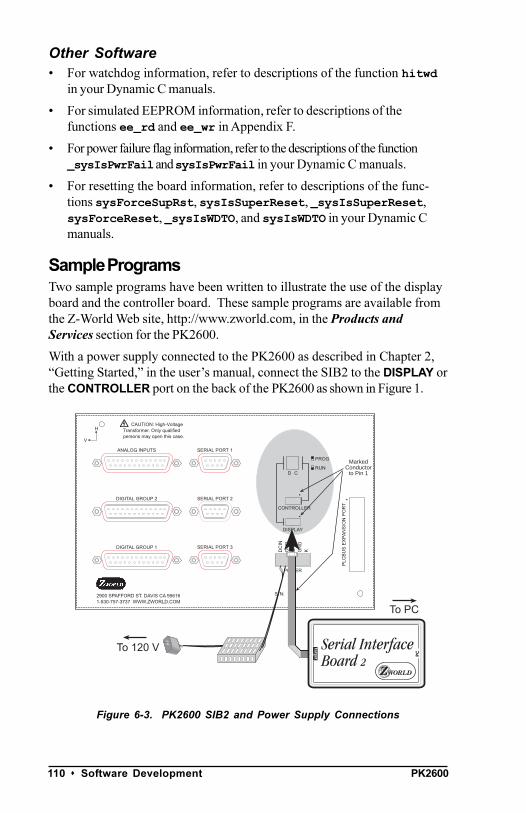
PK2600110 s Software Development
Other Software For watchdog information, refer to descriptions of the function hitwd
in your Dynamic C manuals.
For simulated EEPROM information, refer to descriptions of thefunctions ee_rd and ee_wr in Appendix F.
For power failure flag information, refer to the descriptions of the function_sysIsPwrFail and sysIsPwrFail in your Dynamic C manuals.
For resetting the board information, refer to descriptions of the func-tions sysForceSupRst, sysIsSuperReset, _sysIsSuperReset,sysForceReset, _sysIsWDTO, and sysIsWDTO in your Dynamic Cmanuals.
Sample ProgramsTwo sample programs have been written to illustrate the use of the displayboard and the controller board. These sample programs are available fromthe Z-World Web site, http://www.zworld.com, in the Products andServices section for the PK2600.
With a power supply connected to the PK2600 as described in Chapter 2,Getting Started, in the users manual, connect the SIB2 to the DISPLAY orthe CONTROLLER port on the back of the PK2600 as shown in Figure 1.
Figure 6-3. PK2600 SIB2 and Power Supply Connections
PROG
RUN
CAUTION: High-VoltageTransformer. Only qualifiedpersons may open this case.
S/N:
CONTROLLER
POWER
DISPLAY
GN
DG
ND
DC
IN
KGN
D
PLC
BU
S E
XP
AN
SIO
N P
OR
T
DIGITAL GROUP 2
ANALOG INPUTS
DIGITAL GROUP 1
SERIAL PORT 1
SERIAL PORT 2
SERIAL PORT 3
D C
2900 SPAFFORD ST. DAVIS CA 956161-530-757-3737 WWW.ZWORLD.COM
H
V
To PC
To 120 V
MarkedConductor
to Pin 1
With Dynamic C installed on your PC, download the PK26CONT.C and thePK26DISP.C sample programs from the Z-World Web site.
PK26CONT.C illustrates the use of the controller board. UsePK26CONT.C with the SIB2 connected to the CONTROLLER header onthe back of the PK2600.
PK26DISP.C illustrates the use of the display board. Use PK26DISP.Cwith the SIB2 connected to the DISPLAY header on the back of thePK2600.
The communication rate, port, and protocol are all selected by choosingSerial Options from Dynamic Cs OPTIONS menu. The SIB2 and thePK2600 both set their baud rate automatically to match the communicationrate set on the host PC using Dynamic C (9600 bps, 19,200 bps, 28,800 bpsor 57,600 bps). To begin, use the default communication rate of 19,200 bps.
Make sure that the PC serial port used to connect the serial cable (COM1or COM2) is the one selected in the Dynamic C OPTIONS menu. Select the1-stop-bit protocol.
Depending on whether the SIB2 is connected to the CONTROLLER or tothe DISPLAY header, select PK26CONT.C or PK26DISP.C, and compile andrun the program by pressing F9 or by selecting Run from the Run menu.
PK2600 Graphics Programming s 111

PK2600112 s Graphics Programming
Blank

PK2600 Graphics Programming s 113
CHAPTER 7:
GRAPHICS PROGRAMMING
Chapter 5 provides helpful guidelines for drawing graphics on the PK2600.
PK2600114 s Graphics Programming
InitializationThe PK2600, unlike most other Z-World controllers, uses the maximum I/Oand memory wait states when main() gets control. The wait states can bereduced to improve performance. The following statement sets up theproper wait states for the standard (using a 90 ns flash memory) PK2600display board.
outport(DCNTL,(inport(DCNTL)&0xf)|0x60);
The graphic LCD can be set up by a simple function call to
glInit();
This function initializes and starts the LCD controller before supplyingvoltage to the LCD screen.
The backlight is controlled by op71BackLight(int onOff). Pass zero toturn off the backlight (default) or a non-zero value to turn on the backlight.
If you have a PK2600 equipped with software contrast control, callop71SetContrast(unsigned level) to change contrast. The range oflevel is from 0 to 127. A level of 63 usually yields reasonable contrast atroom temperature.
Drawing PrimitivesYou can draw various objects on the LCD. Before doing any drawing,specify the type of the "brush" by calling glSetBrushType(int flag).Four brush macros are supported:
GL_SET sets the pixels as specified by the plot commands, but leavesother pixels alone;
GL_CLEAR clears the pixels as specified by the plot commands, butleaves other pixels alone;
GL_XOR toggles the pixels as specified by the plot command, butleaves other pixels alone;
GL_BLOCK forces the value of pixels in groups of eight vertical pixels.GL_BLOCK is useful when speed is important, the current pixelsneed to be overwritten, and the overwriting pixels are aligned ineight-pixel rows.
Plot a Pixel int glPlotDot(int x, int y);
x and y are the coordinates, the upper left corner is (0,0).

PK2600 Graphics Programming s 115
Plot a Line void glPlotLine(int x1, int y1, int x2, int y2);
(x1,y1) and (x2,y2) are the endpoints of the line.
Plot a Circle void glPlotCircle(int xc, int yc, int r);
(xc,yc) is the center of the circle, r is the radius.
Plot a Polygon void glPlotPolygon(int n, int x1, int y1,...);
n is the number of vertices, (x1,y1) is the first vertex, followed by theother vertices in the x-first order.
Fill a Circle void glFillCircle(int xc, int yc, int r);
Similar to glPlotCircle, but paints the circle solid.
Fill a Polygon void glFillPolygon(int n, int x1, int y1,...);
Similar to glPlotPolygon, but paints the polygon solid. Note thatthis function works for polygons with concave angles.
Draw a Bitmap void glPutBitmap(int x, int y, int w, int h,
char *bm);
or
void glXPutBitmap(int x, int y, int w, int h,unsigned long xBm);
(x,y) is the location of the upper left corner of the bitmap, w is thewidth, h is the height of the bitmap, bm points to the first byte of thebitmap, xBm is the physical address of the bitmap if the bitmap is storedin xmem (instead of root memory).

PK2600116 s Graphics Programming
Printing TextPrinting text involves setting the font information structures. Call
void glFontInit(struct _fontInfo *pInfo,char pixWidth, char pixHeight,unsigned startChar, unsigned endChar, char *bitmapBuffer);
to initialize a font information structure if the font is stored in root memory.pInfo points to a font information structure, pixWidth is the width ofeach character (fixed pitch), pixHeight is the height of each character,startChar is the ASCII code of the first character in the font, endChar isthe ASCII code of the last character in the font, and bitmapBuffer pointsto the font table stored in root memory.
Call
void glXFontInit(struct _fontInfo *pInfo,char pixWidth, char pixHeight,unsigned startChar, unsigned endChar, unsigned long xmemBuffer);
to initialize a font information structure if the font is stored in xmem. This issimilar to glFontInit, but xmemBuffer is a physical address pointing tothe font table stored in xmem.
Z-World supplies five font sizes for the PK2600. The smallest font,engFont6x8, compiles to xmem, and each character is 6 pixels wide by 8pixels high. The largest font, engFont17x35, also compiles to xmem, andeach character is 17 pixels wide by 35 pixels high.
When you need to print text to the LCD, call
void glPrintf(int x, int y,struct _fontInfo *pInfo, char *fmt,...);
where (x,y) is the upper left corner of the text, pInfo points to a fontinformation structure, fmt points to a format string (much like printf),and the rest of the parameters specify what to print for each field in theformat string (same as printf).
PK2600 Graphics Programming s 117
Keypad ProgrammingThe sample program KPDEFLT.C in the Dynamic C SAMPLES\QVGA subdirec-tory demonstrates how to read the keypad. Add the following directives atthe top of the program to make it possible to use the keypad routines.
#use lqvga.lib (landscape orientation) OR#use pqvga.lib (portrait orientation)
#use ezioop71.lib
#use kp_op71.lib
InitializationTo initialize the keypad driver, call kpDefInit(). This must be performedbefore other keypad operations.
Scanning the KeypadThe function kpScanState() must be called periodically to scan thekeypad for changes. In a cooperative multitasking (big-loop style), thisfunction should be called every 25 ms or so. If you are using a real-timekernel, you can also attach this function to one of the tasks and have itinvoked approximately every 25 ms. Note that this function scans forchanges, but it does not report what was changed.
Reading Keypad ActivitiesThe function kpDefGetKey() returns the interpretation of the statechange detected by kpScanState() into key activities. The means thatthe kpDefGetKey() function must be called no less frequently thankpScanState() to ensure no key activity is lost. The functionkpDefGetKey() returns an integer. If the integer is 1, no key activitywas detected. Otherwise, bits 02 indicates the index of the sense line ofthe key (= column), and bits 35 indicate the index of the drive line of thekey (= row). Bit 8 indicates whether the key has been "pressed"the keywas pressed if bit 8 is a 1.
Note that if two key activities occur between two calls to kpScanState(),only one key activity is interpreted by the kpDefGetKey() function eventhough both activities may be registered by the kpScanState() function.The priority of key interpretation is from drive line 0 (highest priority) todrive line 7. On the same drive line, the priority is from sense line 0(highest priority) to sense line 7.
Once a key activity is detected by kpScanState(), no further keyactivities will be detected by further calls to kpScanState() unlesskpDefGetKey() is called.

PK2600118 s Graphics Programming
Font and Bitmap ConversionCustomers are encouraged to design their own fonts and bitmaps. Theserestrictions must be followed.
Save bitmaps as Windows bitmaps ( .bmp), not OS/2 bitmaps.
The bitmap can only have two colors. Color 0 is the background, andcolor 1 is the foreground. This is the reverse of most bitmap editors.
Fonts must be bitmapped (not true type) and must be of fixed pitch.
Save font files as .fnt (version 3).
The PK2600 uses a "vertical stripe" display logic format. The conversionutility programs fntstrip.exe (landscape image) and fntcvtr.exe(portrait image) convert the .fnt and .bmp file format to the Z-Worldvertical stripe format.
Follow these instructions to use these utilities.
1. Create the .fnt or .bmp file that conforms to the restrictions listedabove.
2. Start fntstrip or fntcvtr.
3. Specify the file to convert (select the file from the menu List files oftype), and choose either .fnt or .bmp.
Entering *.fnt or *.bmp in the File name window will notwork. The file must be selected after clicking on Font files orBitmap files in the List files of type window.
4. Click the OK button or double-click on the file to convert. At this point,the software asks the destination of the conversion. Specify a file tostore the result (text file) of the conversion. Click OK when the file isspecified.
5. The title bar displays "[inactive]" when the conversion is done. Closethe window.
Dynamic C may be used to edit the text file that was generated. Thegenerated file typically looks as follows.
/*Automatic output from Font Converterfont file is U:\TEST\DC5X\SAMPLES\QVGA\6X8.OUT.dfVersion = 0x300dfSize = 5148dfCopyright = (c) Copyright 1997,1998 Z-World. All
rights reserved.dfType = 0x0horizontal size is 6 pixels.vertical size is 8 pixels.first character is for code 0x20.
Tip

PK2600 Graphics Programming s 119
last character is for code 0xff.make call to glFontInit(&fi, 6, 8, 32, 127, fontBitMap)to initialize table*/
char fontBitMap[] = /* char 0x20 of width 6 at 0x5da */'\x0','\x0','\x0','\x0','\x0','\x0',...'\x0';
The first task is to rename the array so that it is unique. Then you candecide whether the font/bitmap should be stored in root memory or inextended memory. Because bitmaps can be large and root memory space isprecious, Z-World recommends you to use xmem to store the font/bitmap.To store the font/bitmap in xmem, you need to change the following line.
char fontBitMap[] =
to
xdata fontBitMap
Once these changes are made, you can copy and paste the font (as aninitialized character array or as an initialized xdata item) into your programor library.
Remember to #use either the LQVGA.LIB (landscape image) orthe PQVGA.LIB (portrait image) library in your program.
Using the Font/Bitmap In Your ProgramThe array does not store the dimensions of the font or the bitmap. Thisinformation is contained in the comments. The following lines in thecomments indicate the dimensions of the font.
/*horizontal size is 6 pixels.vertical size is 8 pixels.*/
For fonts, the comments also indicate the starting character and the endingcharacter code with the following line.
/*make call to glFontInit(&fi, 6, 8, 32, 127, fontBitMap)*/
The fourth argument is the first character code mapped to the font and thefifth argument is the last character code mapped to the font.
!

PK2600120 s Graphics Programming
To initialize a font information structure (of type struct _fontInfo), youcan call glFontInit for a font stored in root memory or glXFontInit fora font stored in xmem.
To display a bitmap, call glPutBitmap to display a bitmap stored in rootmemory, and call glXPutBitmap to display a bitmap stored in xmem.

PK2600 Troubleshooting s 121
APPENDIX A: TROUBLESHOOTING
Appendix A provides procedures for troubleshooting system hardwareand software. The following sections are included.
Out of the Box
Dynamic C Will Not Start
Finding the Correct COM Port and Baud Rate
PK2600 Repeatedly Resets
Troubleshooting Software
PK2600122 s Troubleshooting
Out of the BoxCheck the items listed below before starting development. Rechecking mayhelp to solve problems found during development.
Do not connect any boards with PLCBus, RS-485 or any other I/Odevices until you verify that the PK2600 runs standalone.
Verify that your entire system has a good, low-impedance ground. ThePK2600 is often connected between the PC and some other device.Any differences in ground potential from unit to unit can cause serious,hard-to-diagnose problems.
Double-check the connecting cables.
Do not connect analog ground to digital ground anywhere.
Verify that your PCs COM port actually works. Try connecting aknown-good serial device to your COM port. Remember that on a PCCOM1/COM3 and COM2/COM4 share interrupts. User shells andmouse software, particularly, often interfere with proper COM-portoperation. For example, a mouse running on COM1 can preclude yourrunning Dynamic C on COM3, unless the interrupt is changed.
Use the supplied Z-World power supply. If you must use your ownpower supply, verify that it has enough capacity and filtering tosupport the PK2600.
Use the supplied Z-World cables. The most common fault of home-made cables is their failure to properly assert CTS at the RS-232 port ofthe PK2600. Without CTSs being asserted, the PK2600s RS-232 portwill not transmit. You can assert CTS by either connecting the RTSsignal of the PCs COM port or looping back the PK2600s RTS.
Experiment with each peripheral device you connect to your PK2600 todetermine how it appears to the PK2600 when it is powered up, pow-ered down, when its connecting wiring is open, and when its connect-ing wiring is shorted..
PK2600 Troubleshooting s 123
Dynamic C Will Not StartIf Dynamic C will not start, an error message on the Dynamic C screen (forexample, Target Not Responding or Communication Error), announces acommunication failure. The following list describes situations causing anerror message and possible resolutions.
Wrong Communication Mode Both sides must be talking RS-232.
Wrong COM Port A PC generally has two serial ports, COM1 andCOM2. Specify the one being used in the Dynamic C Target Setupmenu. Use trial and error, if necessary.
Some PCs have special programs to reconfigure their portassignments. You may need to run such a program to make agiven COM port appear at an external back panel Dconnector.
Wrong Operating Mode Communication with Dynamic C will be lostwhen the PK2600 is configured for standalone operation. Make surethe DIP switch on the back of the PK2600 is set to PROGRAM mode asdescribed in Chapter 2, Getting Started, for the controller board or thedisplay, depending on which board is to be programmed.
You need to reset the PK2600 by unplugging the transformer from thewall, waiting a moment, then plugging the transformer back.
If all else fails, connect the serial cable to the PK2600 after power up. If thePCs RS-232 port supplies a large current (most commonly on portable andindustrial PCs), some RS-232 level converter ICs go into a nondestructivelatch-up. Connect the RS-232 cable after power up to eliminate thisproblem.
PK2600 Repeatedly ResetsIf the program fails to hit the watchdog timer periodically, the watchdogtimer causes a reset every 1.0 seconds. When you debug a program usingthe Dynamic C debugger, Dynamic C hits the watchdog timer. If yourprogram does not hit the watchdog timer , then you will have troublerunning your program in standalone mode. (To hit the watchdog, make acall to the Dynamic C library function hitwd).
Dynamic C Loses Serial LinkIf your program disables interrupts for a more than 50 ms, Dynamic C maylose its link with the PK2600.
!

PK2600124 s Troubleshooting
Common Programming Errors Values for constants or variables out of range. Table A-1 lists accept-
able ranges for variables and constants.
Mismatched types. For example, the literal constant 3293 is of typeint (16-bit integer). However, the literal constant 3293.0 is of type float.Although Dynamic C can handle some type mismatches, avoiding typemismatches is the best practice.
Counting up from, or down to, one instead of zero. In software, ordinalseries often begin or terminate with zero, not one.
Confusing a functions definition with an instance of its use in a listing.
Not ending statements with semicolons.
Not inserting commas as required in functions parameter lists.
Leaving out ASCII space character between characters forming adifferent legalbut unwantedoperator.
Confusing similar-looking operators such as && with &,== with =, and // with /.
Inadvertently inserting ASCII nonprinting characters into a source-code file.
If the DMA-driven PWM correctly drives the output for a while, thensuddenly some channels remain ON, others remain off, most likely thefunction _eioBrdAORf() is not called frequently enough. There arethree possible solutions.
1. Increase the frequency of calling _eioBrdAORf().
2. Increase the size of the waveform pattern buffer.
3. Slow down the clock CKA1.
Table A-1. Ranges of Dynamic CFunction Types
Type Range
int –32,768 (–215) to+32,767 (215 – 1)
long int −2,147,483,648 (−231) to+2147483647 (231 – 1)
float 1.18 × 10-38 to3.40 × 1038
char 0 to 255

PK2600 Specifications s 125
APPENDIX B: SPECIFICATIONS
Appendix B provides comprehensive PK2600 physical, electronic andenvironmental specifications.
PK2600126 s Specifications
Electronic and Mechanical SpecificationsTable B-1 lists the electronic, mechanical, and environmental specificationsfor the PK2600.
Table B-1. PK2600 General Specifications
Parameter Specification
Enclosure BackCover Size
4.511″ × 6.930″ × 2.500″(115 mm × 175 mm × 63.5 mm)
Front Bezel Size8.00" × 5.4" × 0.156"(203 mm × 137 mm × 4.0 mm)
with gasket
Operating Temperature 0°C to 50°C, may be stored at –20°C to 70°C
Humidity 25% to 65%, noncondensing
Power15 V DC to 30 V DC, 8.7 W with backlight on,5.7 W with backlight off
BacklightReplaceable dual cold-cathode fluorescent tuberated at 20,000 h to 30,000 h with softwareon/off control
LCD
FSTN, 320 × 240 pixels, blue on white back-ground. Pixel matrix is 115.2 mm × 86.4 mm,0.36 mm pitch. Viewing area is 121 mm ×91 mm. Adjustable contrast with temperaturecompensation.
Touchscreen8 × 8 matrix, 225 touch switches rated 106 con-tacts
Digital Inputs
16 standard, continuous operation from –20 V to+24 V, logic threshold at 2.5 V, protected againstspikes ±48 V, 10 kΩ pull-up or pull-down resis-tors
Digital Outputs16 standard, at 25°C one channel can sink up to500 mA continuously, load limit is 48 V
Analog InputsTen 12-bit channels:• 8 conditioned, factory configured 0 V to 10 V• 2 unconditioned, 0 V to 2.5 V
Analog OutputsPulse-width modulated, on digital output lines, upto 7 channels
ProcessorZ180 at 18.432 MHz (controller)Z180 at 18.432 MHz (display)
continued…

PK2600 Specifications s 127
Table B-1. PK2600 General Specifications (concluded)
Parameter Specification
SRAM32K standard, supports up to 512K (controller)128K standard, supports up to 512K (display)
VRAM 32K standard, supports up to 64K (display)
Flash EPROM128K standard, supports up to 256K (controller)Two 256K (display)
EEPROM Simulated in flash EPROM
Serial Ports• 1 full-duplex RS-232• 2 configurable as full-duplex RS-232 or as
RS-485
Serial Rate Up to 57,600 bps
Watchdog Yes
Time/Date Clock Yes (controller and display)
Backup Battery
• Panasonic BR2325-1HG 3 V DC lithium ion,rated life 190 mA"h (controller)
• Renata CR2325RH 3 V DC lithium ion, ratedlife 165 mA⋅h (display)
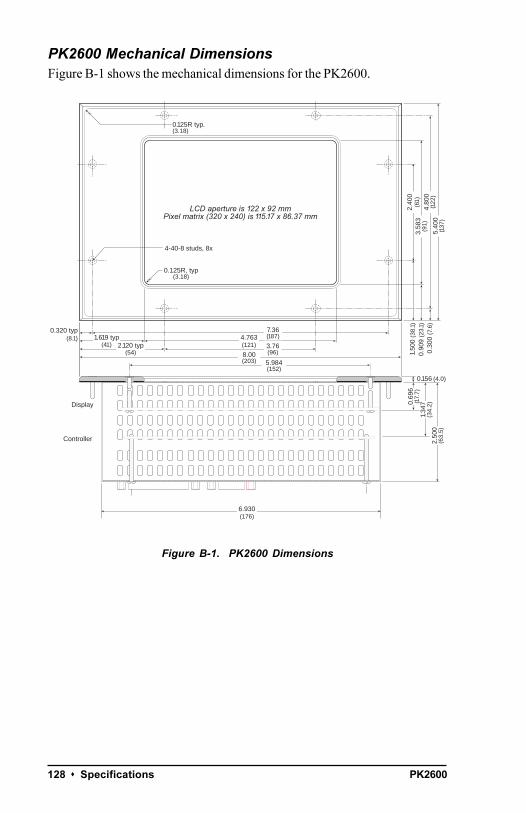
PK2600128 s Specifications
PK2600 Mechanical DimensionsFigure B-1 shows the mechanical dimensions for the PK2600.
Figure B-1. PK2600 Dimensions
2.50
0(6
3.5)
Display
0.156 (4.0)
Controller
0.30
0 (7
.6)
0.90
9 (2
3.1)
1.50
0 (3
8.1)
LCD aperture is 122 x 92 mmPixel matrix (320 x 240) is 115.17 x 86.37 mm
8.00(203)
4-40-8 studs, 8x
1.619 typ(41)
7.36(187)
2.120 typ(54)
4.763(121) 3.76
(96)
5.984(152)
0.125R, typ(3.18)
2.40
0(6
1)3.
583
(91)
4.80
0(1
22)
5.40
0(1
37)
0.125R typ.(3.18)
0.320 typ(8.1)
0.69
6(1
7.7)
1.34
7(3
4.2)
6.930(176)
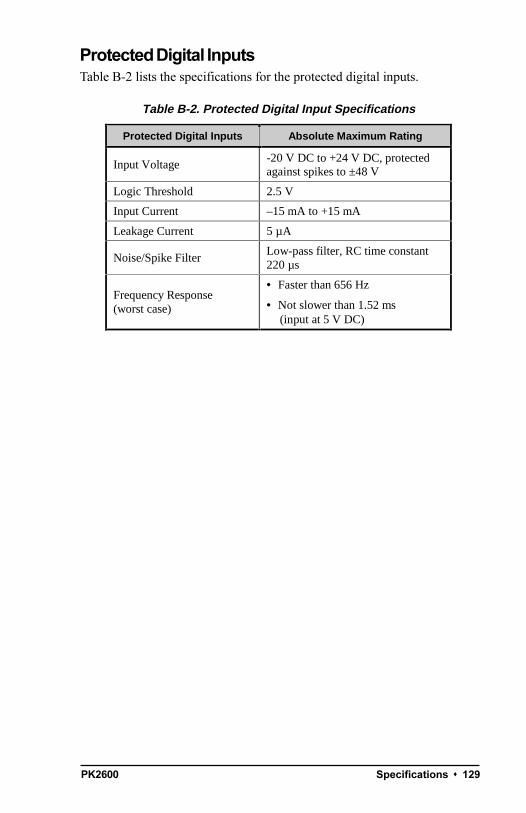
PK2600 Specifications s 129
Table B-2. Protected Digital Input Specifications
Protected Digital Inputs Absolute Maximum Rating
Input Voltage -20 V DC to +24 V DC, protectedagainst spikes to ±48 V
Logic Threshold 2.5 V
Input Current –15 mA to +15 mA
Leakage Current 5 µA
Noise/Spike FilterLow-pass filter, RC time constant220 µs
Frequency Response(worst case)
• Faster than 656 Hz
• Not slower than 1.52 ms(input at 5 V DC)
Protected Digital InputsTable B-2 lists the specifications for the protected digital inputs.
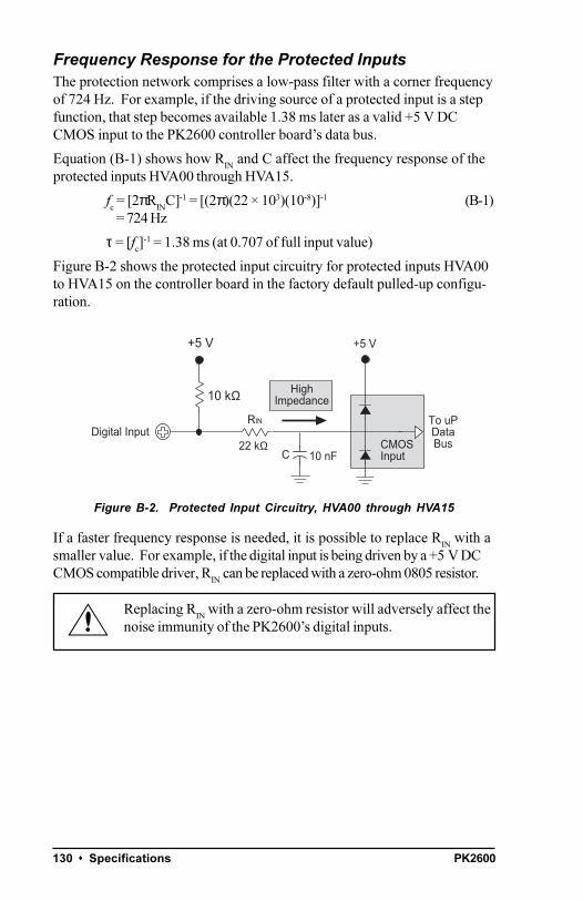
PK2600130 s Specifications
Frequency Response for the Protected InputsThe protection network comprises a low-pass filter with a corner frequencyof 724 Hz. For example, if the driving source of a protected input is a stepfunction, that step becomes available 1.38 ms later as a valid +5 V DCCMOS input to the PK2600 controller boards data bus.
Equation (B-1) shows how RIN
and C affect the frequency response of theprotected inputs HVA00 through HVA15.
fc = [2πR
INC]-1 = [(2π)(22 × 103)(10-8)]-1 (B-1)
fc = 724 Hz
τ = [fc]-1 = 1.38 ms (at 0.707 of full input value)
Figure B-2 shows the protected input circuitry for protected inputs HVA00to HVA15 on the controller board in the factory default pulled-up configu-ration.
Figure B-2. Protected Input Circuitry, HVA00 through HVA15
If a faster frequency response is needed, it is possible to replace RIN
with asmaller value. For example, if the digital input is being driven by a +5 V DCCMOS compatible driver, R
IN can be replaced with a zero-ohm 0805 resistor.
Replacing RIN
with a zero-ohm resistor will adversely affect thenoise immunity of the PK2600s digital inputs.
CMOSInput
HighImpedance
22 kΩ10 nF
Digital Input
+5 V
To uPDataBus
C
RIN
10 kΩ
+5 V
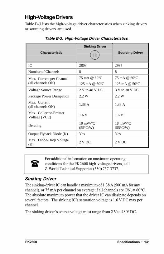
PK2600 Specifications s 131
(
High-Voltage DriversTable B-3 lists the high-voltage driver characteristics when sinking driversor sourcing drivers are used.
For additional information on maximum operatingconditions for the PK2600 high-voltage drivers, callZ-World Technical Support at (530) 757-3737.
Sinking DriverThe sinking-driver IC can handle a maximum of 1.38 A (500 mA for anychannel), or 75 mA per channel on average if all channels are ON, at 60°C.The absolute maximum power that the driver IC can dissipate depends onseveral factors. The sinking ICs saturation voltage is 1.6 V DC max perchannel.
The sinking drivers source voltage must range from 2 V to 48 V DC.
Table B-3. High-Voltage Driver Characteristics
Characteristic
Sinking Driver
Sourcing Driver
IC 2803 2985
Number of Channels 8 8
Max. Current per Channel(all channels ON)
75 mA @ 60°C
125 mA @ 50°C
75 mA @ 60°C
125 mA @ 50°C
Voltage Source Range 2 V to 48 V DC 3 V to 30 V DC
Package Power Dissipation 2.2 W 2.2 W
Max. Current(all channels ON)
1.38 A 1.38 A
Max. Collector-EmitterVoltage (VCE)
1.6 V 1.6 V
Derating18 mW/°C(55°C/W)
18 mW/°C(55°C/W)
Output Flyback Diode (K) Yes Yes
Max. Diode-Drop Voltage(K)
2 V DC 2 V DC
FD
PK2600132 s Specifications
$
Sourcing DriverThe sourcing-driver IC can handle a maximum of 1.38 A (250 mA for anychannel), or 75 mA per channel on average if all channels are ON, at 60°C.The sourcing IC can dissipate a maximum of 2.2 W. The saturation voltageis 1.6 V DC max per channel.
The sourcing drivers source voltage must range from 3 V to 30V DC. The minimum output sustaining voltage is 15 V DC.Operating the driver at more than 15 V without providing forenergy dissipation may destroy the driver when an inductiveload is connected.
For more information on sinking and sourcing high-voltagedrivers, refer to the Motorola (DL128) or Allegro (AMS 502Z)linear data books.

PK2600 Memory, I/O Map, and Interrupt Vectors s 133
APPENDIX C: MEMORY,I/O MAP, AND INTERRUPT VECTORS
Appendix C provides detailed information on memory and an I/O map. Theinterrupt vectors are also listed.
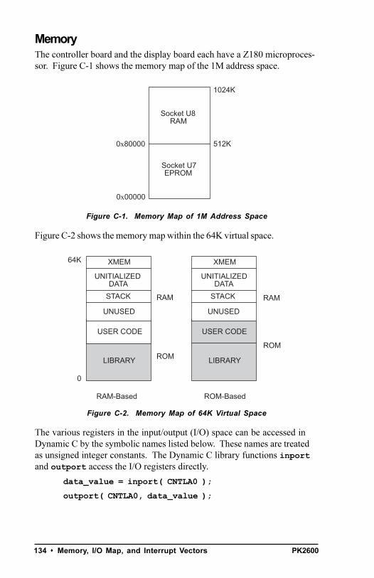
PK2600134 s Memory, I/O Map, and Interrupt Vectors
MemoryThe controller board and the display board each have a Z180 microproces-sor. Figure C-1 shows the memory map of the 1M address space.
Figure C-1. Memory Map of 1M Address Space
Figure C-2 shows the memory map within the 64K virtual space.
Figure C-2. Memory Map of 64K Virtual Space
The various registers in the input/output (I/O) space can be accessed inDynamic C by the symbolic names listed below. These names are treatedas unsigned integer constants. The Dynamic C library functions inportand outport access the I/O registers directly.
data_value = inport( CNTLA0 );
outport( CNTLA0, data_value );
UNITIALIZEDDATA
USER CODE
LIBRARY
RAM
ROM
RAM
ROM
UNUSED
RAM-Based ROM-Based
0
STACK
XMEM64K
UNITIALIZEDDATA
USER CODE
LIBRARY
UNUSED
STACK
XMEM
512K
1024K
Socket U8RAM
Socket U7EPROM
0x00000
0x80000
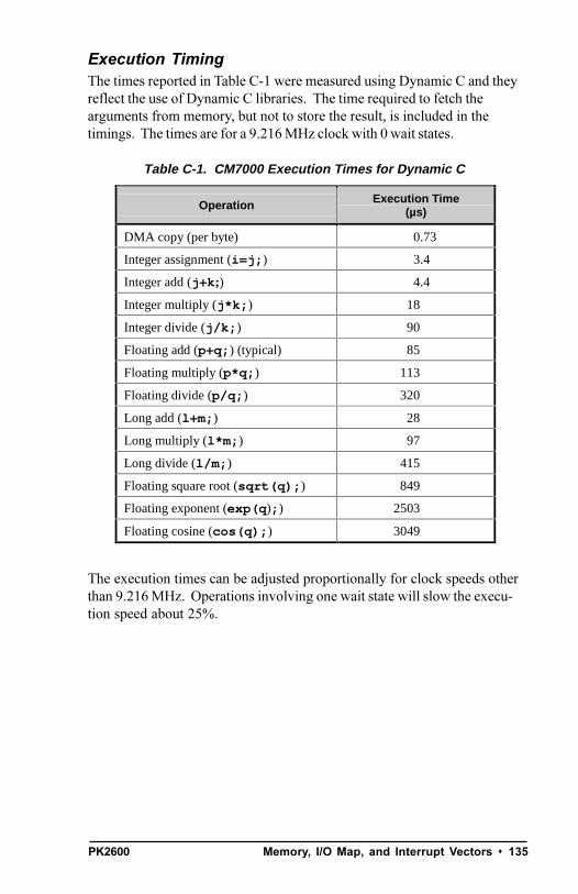
PK2600 Memory, I/O Map, and Interrupt Vectors s 135
Table C-1. CM7000 Execution Times for Dynamic C
Operation Execution Time(µs)
DMA copy (per byte) 0.73
Integer assignment (i=j;) 3.4
Integer add (j+k;) 4.4
Integer multiply (j*k;) 18
Integer divide (j/k;) 90
Floating add (p+q;) (typical) 85
Floating multiply (p*q;) 113
Floating divide (p/q;) 320
Long add (l+m;) 28
Long multiply (l*m;) 97
Long divide (l/m;) 415
Floating square root (sqrt(q);) 849
Floating exponent (exp(q);) 2503
Floating cosine (cos(q);) 3049
Execution TimingThe times reported in Table C-1 were measured using Dynamic C and theyreflect the use of Dynamic C libraries. The time required to fetch thearguments from memory, but not to store the result, is included in thetimings. The times are for a 9.216 MHz clock with 0 wait states.
The execution times can be adjusted proportionally for clock speeds otherthan 9.216 MHz. Operations involving one wait state will slow the execu-tion speed about 25%.
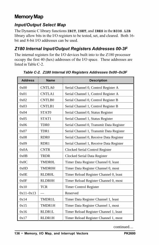
PK2600136 s Memory, I/O Map, and Interrupt Vectors
Table C-2. Z180 Internal I/O Registers Addresses 0x00–0x3F
Address Name Description
0x00 CNTLA0 Serial Channel 0, Control Register A
0x01 CNTLA1 Serial Channel 1, Control Register A
0x02 CNTLB0 Serial Channel 0, Control Register B
0x03 CNTLB1 Serial Channel 1, Control Register B
0x04 STAT0 Serial Channel 0, Status Register
0x05 STAT1 Serial Channel 1, Status Register
0x06 TDR0 Serial Channel 0, Transmit Data Register
0x07 TDR1 Serial Channel 1, Transmit Data Register
0x08 RDR0 Serial Channel 0, Receive Data Register
0x09 RDR1 Serial Channel 1, Receive Data Register
0x0A CNTR Clocked Serial Control Register
0x0B TRDR Clocked Serial Data Register
0x0C TMDR0L Timer Data Register Channel 0, least
0x0D TMDR0H Timer Data Register Channel 0, most
0x0E RLDR0L Timer Reload Register Channel 0, least
0x0F RLDR0H Timer Reload Register Channel 0, most
0x10 TCR Timer Control Register
0x11–0x13 — Reserved
0x14 TMDR1L Timer Data Register Channel 1, least
0x15 TMDR1H Timer Data Register Channel 1, most
0x16 RLDR1L Timer Reload Register Channel 1, least
0x17 RLDR1H Timer Reload Register Channel 1, most
continued…
Memory Map
Input/Output Select MapThe Dynamic C library functions IBIT, ISET, and IRES in the BIOS.LIBlibrary allow bits in the I/O registers to be tested, set, and cleared. Both 16-bit and 8-bit I/O addresses can be used.
Z180 Internal Input/Output Registers Addresses 00-3FThe internal registers for the I/O devices built into to the Z180 processoroccupy the first 40 (hex) addresses of the I/O space. These addresses arelisted in Table C-2.
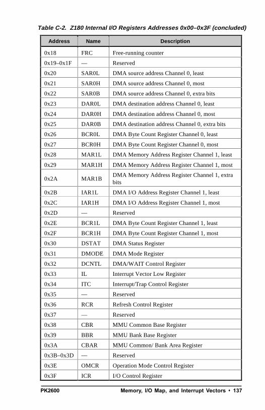
PK2600 Memory, I/O Map, and Interrupt Vectors s 137
Table C-2. Z180 Internal I/O Registers Addresses 0x00–0x3F (concluded)
Address Name Description
0x18 FRC Free-running counter
0x19–0x1F — Reserved
0x20 SAR0L DMA source address Channel 0, least
0x21 SAR0H DMA source address Channel 0, most
0x22 SAR0B DMA source address Channel 0, extra bits
0x23 DAR0L DMA destination address Channel 0, least
0x24 DAR0H DMA destination address Channel 0, most
0x25 DAR0B DMA destination address Channel 0, extra bits
0x26 BCR0L DMA Byte Count Register Channel 0, least
0x27 BCR0H DMA Byte Count Register Channel 0, most
0x28 MAR1L DMA Memory Address Register Channel 1, least
0x29 MAR1H DMA Memory Address Register Channel 1, most
0x2A MAR1BDMA Memory Address Register Channel 1, extrabits
0x2B IAR1L DMA I/O Address Register Channel 1, least
0x2C IAR1H DMA I/O Address Register Channel 1, most
0x2D — Reserved
0x2E BCR1L DMA Byte Count Register Channel 1, least
0x2F BCR1H DMA Byte Count Register Channel 1, most
0x30 DSTAT DMA Status Register
0x31 DMODE DMA Mode Register
0x32 DCNTL DMA/WAIT Control Register
0x33 IL Interrupt Vector Low Register
0x34 ITC Interrupt/Trap Control Register
0x35 — Reserved
0x36 RCR Refresh Control Register
0x37 — Reserved
0x38 CBR MMU Common Base Register
0x39 BBR MMU Bank Base Register
0x3A CBAR MMU Common/ Bank Area Register
0x3B–0x3D — Reserved
0x3E OMCR Operation Mode Control Register
0x3F ICR I/O Control Register
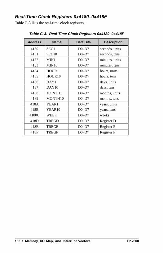
PK2600138 s Memory, I/O Map, and Interrupt Vectors
Real-Time Clock Registers 0x41800x418FTable C-3 lists the real-time clock registers.
Table C-3. Real-Time Clock Registers 0x4180–0x418F
Address Name Data Bits Description
4180 SEC1 D0–D7 seconds, units
4181 SEC10 D0–D7 seconds, tens
4182 MIN1 D0–D7 minutes, units
4183 MIN10 D0–D7 minutes, tens
4184 HOUR1 D0–D7 hours, units
4185 HOUR10 D0–D7 hours, tens
4186 DAY1 D0–D7 days, units
4187 DAY10 D0–D7 days, tens
4188 MONTH1 D0–D7 months, units
4189 MONTH10 D0–D7 months, tens
418A YEAR1 D0–D7 years, units
418B YEAR10 D0–D7 years, tens
4180C WEEK D0–D7 weeks
418D TREGD D0–D7 Register D
418E TREGE D0–D7 Register E
418F TREGF D0–D7 Register F
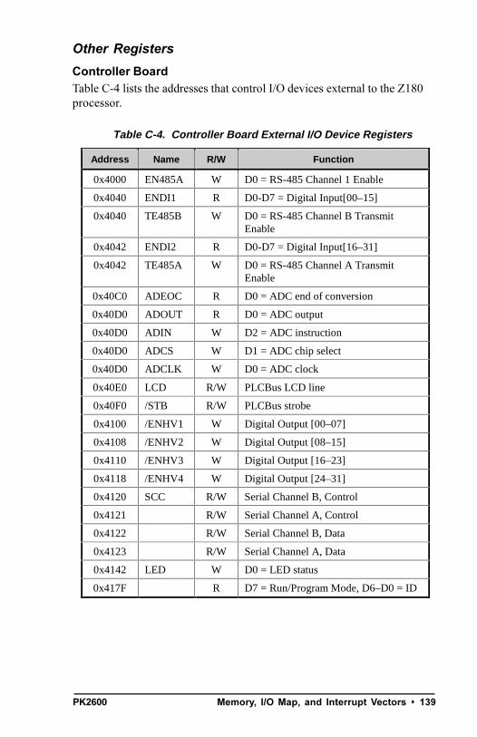
PK2600 Memory, I/O Map, and Interrupt Vectors s 139
Other Registers
Controller BoardTable C-4 lists the addresses that control I/O devices external to the Z180processor.
Table C-4. Controller Board External I/O Device Registers
Address Name R/W Function
0x4000 EN485A W D0 = RS-485 Channel 1 Enable
0x4040 ENDI1 R D0-D7 = Digital Input[00–15]
0x4040 TE485B W D0 = RS-485 Channel B TransmitEnable
0x4042 ENDI2 R D0-D7 = Digital Input[16–31]
0x4042 TE485A W D0 = RS-485 Channel A TransmitEnable
0x40C0 ADEOC R D0 = ADC end of conversion
0x40D0 ADOUT R D0 = ADC output
0x40D0 ADIN W D2 = ADC instruction
0x40D0 ADCS W D1 = ADC chip select
0x40D0 ADCLK W D0 = ADC clock
0x40E0 LCD R/W PLCBus LCD line
0x40F0 /STB R/W PLCBus strobe
0x4100 /ENHV1 W Digital Output [00–07]
0x4108 /ENHV2 W Digital Output [08–15]
0x4110 /ENHV3 W Digital Output [16–23]
0x4118 /ENHV4 W Digital Output [24–31]
0x4120 SCC R/W Serial Channel B, Control
0x4121 R/W Serial Channel A, Control
0x4122 R/W Serial Channel B, Data
0x4123 R/W Serial Channel A, Data
0x4142 LED W D0 = LED status
0x417F R D7 = Run/Program Mode, D6–D0 = ID
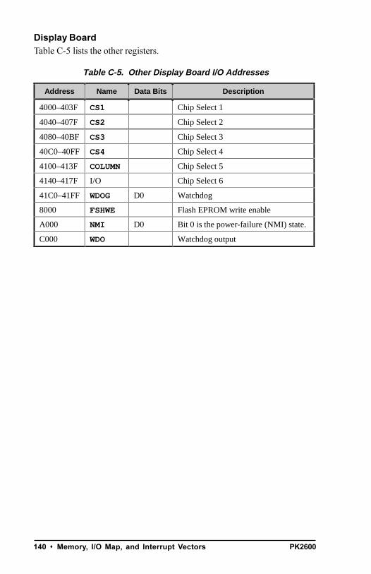
PK2600140 s Memory, I/O Map, and Interrupt Vectors
Table C-5. Other Display Board I/O Addresses
Address Name Data Bits Description
4000–403F CS1 Chip Select 1
4040–407F CS2 Chip Select 2
4080–40BF CS3 Chip Select 3
40C0–40FF CS4 Chip Select 4
4100–413F COLUMN Chip Select 5
4140–417F I/O Chip Select 6
41C0–41FF WDOG D0 Watchdog
8000 FSHWE Flash EPROM write enable
A000 NMI D0 Bit 0 is the power-failure (NMI) state.
C000 WDO Watchdog output
Display BoardTable C-5 lists the other registers.
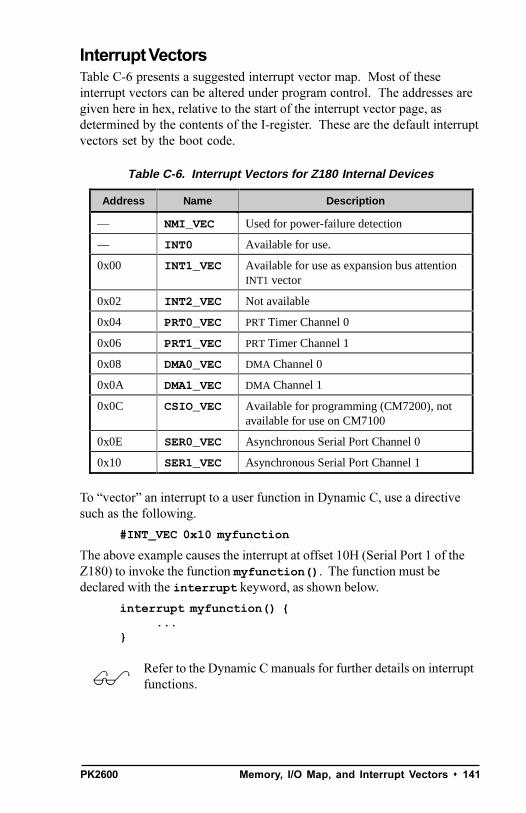
PK2600 Memory, I/O Map, and Interrupt Vectors s 141
$
Interrupt VectorsTable C-6 presents a suggested interrupt vector map. Most of theseinterrupt vectors can be altered under program control. The addresses aregiven here in hex, relative to the start of the interrupt vector page, asdetermined by the contents of the I-register. These are the default interruptvectors set by the boot code.
To vector an interrupt to a user function in Dynamic C, use a directivesuch as the following.
#INT_VEC 0x10 myfunction
The above example causes the interrupt at offset 10H (Serial Port 1 of theZ180) to invoke the function myfunction(). The function must bedeclared with the interrupt keyword, as shown below.
interrupt myfunction() ...
Refer to the Dynamic C manuals for further details on interruptfunctions.
Table C-6. Interrupt Vectors for Z180 Internal Devices
Address Name Description
— NMI_VEC Used for power-failure detection
— INT0 Available for use.
0x00 INT1_VEC Available for use as expansion bus attentionINT1 vector
0x02 INT2_VEC Not available
0x04 PRT0_VEC PRT Timer Channel 0
0x06 PRT1_VEC PRT Timer Channel 1
0x08 DMA0_VEC DMA Channel 0
0x0A DMA1_VEC DMA Channel 1
0x0C CSIO_VEC Available for programming (CM7200), notavailable for use on CM7100
0x0E SER0_VEC Asynchronous Serial Port Channel 0
0x10 SER1_VEC Asynchronous Serial Port Channel 1
PK2600142 s Memory, I/O Map, and Interrupt Vectors
Nonmaskable InterruptsThe /NMI line normally connects to the power-failure output of the 691supervisor. A nonmaskable interrupt (NMI) occurs when PFI falls to 1.25 V± 0.05 V. This advanced warning allows the program to perform someemergency processing before an unwanted power-down occurs.
The NMI is edge-sensitive and cannot be masked by software. Whenactivated, the NMI disables all other interrupts (except TRAP), and beginsexecution from logical address 0x66.
The following example shows how to handle a power-failure interrupt.
#JUMP_VEC NMI_VEC myint
interrupt retn myint()body of interrupt routinewhile(!IBIT(WDO,0))
// input voltage is still below the threshold// that triggered the NMI
return; // if just a power glitch, return
Jump VectorsThese special interrupts occur in a different manner. Instead of loading theaddress of the interrupt routine from the interrupt vector, these interruptscause a jump directly to the address of the vector, which contains a jumpinstruction to the interrupt routine. The following example illustrates ajump vector.
0x66 nonmaskable power-failure interrupt
Since nonmaskable interrupts (NMI) can be used for Dynamic C communi-cations, an interrupt vector for power failure is normally stored just in frontof the Dynamic C program. Use the command
#JUMP_VEC NMI_VEC name
to store the vector here.
The Dynamic C communication routines relay to the jump vector when theNMI is caused by a power failure rather than by a serial interrupt.

PK2600 Memory, I/O Map, and Interrupt Vectors s 143
Table C-7. Interrupt Priorities
Interrupt Priorities
(Highest Priority) Trap (illegal instruction)
NMI (nonmaskable interrupt)
INT 0 (maskable interrupts, Level 0; three modes)
INT 1 (maskable interrupts, Level 1; PLCBusattention line interrupt)
INT 2 (maskable interrupts, Level 2)
PRT Timer Channel 0
PRT Timer Channel 1
DMA Channel 0
DMA Channel 1
Z180 Serial Port 0
(Lowest Priority) Z180 Serial Port 1
Interrupt PrioritiesTable C-7 lists the interrupt priorities.

PK2600144 s Memory, I/O Map, and Interrupt Vectors
Blank
PK2600 Circuit Board Reference s 145
APPENDIX D:
CIRCUIT BOARD REFERENCE
Appendix D provides comprehensive information about the individualboards in the PK2600 assembly.
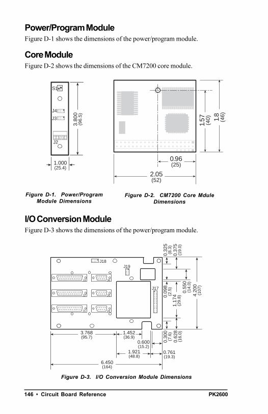
PK2600146 s Circuit Board Reference
Power/Program ModuleFigure D-1 shows the dimensions of the power/program module.
Core ModuleFigure D-2 shows the dimensions of the CM7200 core module.
I/O Conversion ModuleFigure D-3 shows the dimensions of the power/program module.
Figure D-3. I/O Conversion Module Dimensions
Figure D-2. CM7200 Core MduleDimensions
2.05(52)
0.96(25)
1.57
(40) 1.8
(46)
S1
J4
J3
J2
3.80
0(9
6.5)
1.000(25.4)
Figure D-1. Power/ProgramModule Dimensions
J1
J2
J3
J4
J5
J6
J17
J18J19
4.20
0(1
07)
1.17
4(2
9.8)
0.55
0(1
4.0)
0.09
8(2
.5)
0.30
0(7
.6)
0.62
8(1
6.0)
0.32
5(8
.3)
0.37
5(1
9.0)
6.450(164)
1.921(48.8)
0.600(15.2)
0.761(19.3)
3.768(95.7)
1.452(36.9)

PK2600 Circuit Board Reference s 147
Controller BoardFigure D-4 shows the locations of the headers and the dimensions of thecontroller board.
Figure D-4. Controller Board Headers and Dimensions
0.2 typ(5)
1.035(26.3)
2.775(70.5)
3.05(77.5)
4.25(108)
6.25(159)
5.275(134)
3.27
5(8
3.2)
4.20
(107
)
0.92
5(2
3.5)
0.2
typ
(5)
2.54
(64.
5)
4.1(104)
H1
J5
H4
J4
J6
H5
H13H14H15J8
J7
J3
H3 H2J2
H12
J1
SW1
H10H8 H9
H6H7H11
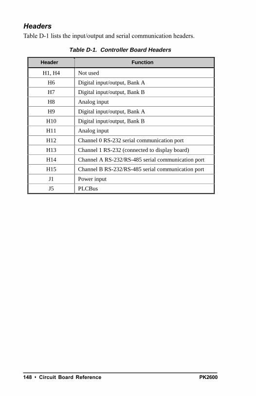
PK2600148 s Circuit Board Reference
HeadersTable D-1 lists the input/output and serial communication headers.
Table D-1. Controller Board Headers
Header Function
H1, H4 Not used
H6 Digital input/output, Bank A
H7 Digital input/output, Bank B
H8 Analog input
H9 Digital input/output, Bank A
H10 Digital input/output, Bank B
H11 Analog input
H12 Channel 0 RS-232 serial communication port
H13 Channel 1 RS-232 (connected to display board)
H14 Channel A RS-232/RS-485 serial communication port
H15 Channel B RS-232/RS-485 serial communication port
J1 Power input
J5 PLCBus

PK2600 Circuit Board Reference s 149
Table D-2. PK2600 Digital Group 1 Pin Mapping
Controller Digital Signal Controller Pin No. PK2600 DB25 Pin No.
HVA00 1 1
HVA01 3 14
HVA02 5 2
HVA03 7 15
GND 9 11, 12, 13
HVA04 2 3
HVA05 4 16
HVA06 6 4
HVA07 8 17
K
Hea
der
H9
10 9, 10
HVA08 1 5
HVA09 3 18
HVA10 5 6
HVA11 7 19
GND 9 24, 25
HVA12 2 7
HVA13 4 20
HVA14 6 8
HVA15 8 21
K
Hea
der
H6
10 22, 23
Table D-2 provides a pin mapping from DIGITAL GROUP 1 to the headerson the controller board.
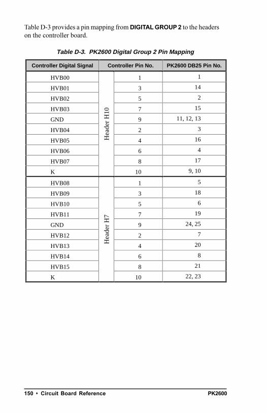
PK2600150 s Circuit Board Reference
Table D-3. PK2600 Digital Group 2 Pin Mapping
Controller Digital Signal Controller Pin No. PK2600 DB25 Pin No.
HVB00 1 1
HVB01 3 14
HVB02 5 2
HVB03 7 15
GND 9 11, 12, 13
HVB04 2 3
HVB05 4 16
HVB06 6 4
HVB07 8 17
K
Hea
der
H10
10 9, 10
HVB08 1 5
HVB09 3 18
HVB10 5 6
HVB11 7 19
GND 9 24, 25
HVB12 2 7
HVB13 4 20
HVB14 6 8
HVB15 8 21
K
Hea
der
H7
10 22, 23
Table D-3 provides a pin mapping from DIGITAL GROUP 2 to the headerson the controller board.
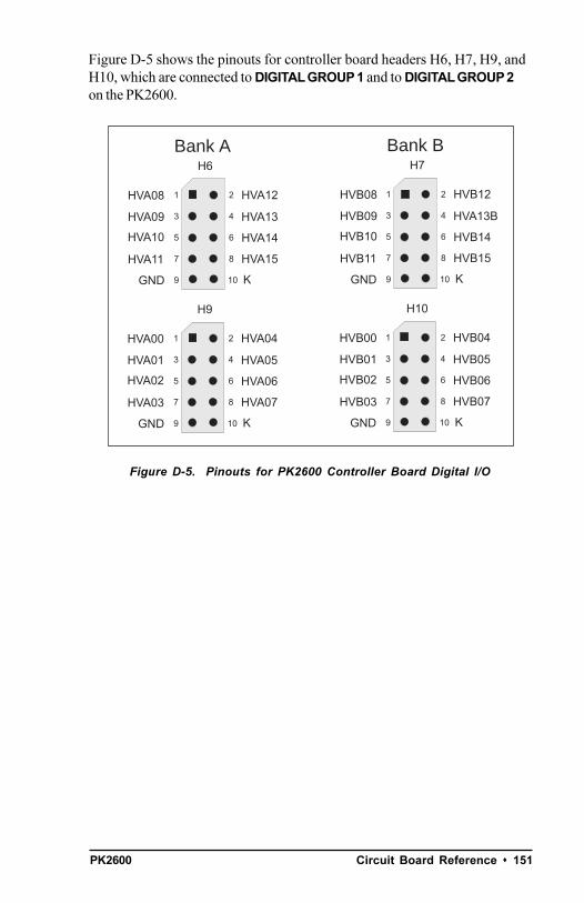
PK2600 Circuit Board Reference s 151
10
H6
1 2
3 4
5 6
7 8
9
HVA08
HVA09
HVA10
HVA11
GND
HVA12
HVA13
HVA14
HVA15
K
10
H9
1 2
3 4
5 6
7 8
9
HVA00
HVA01
HVA02
HVA03
GND
HVA04
HVA05
HVA06
HVA07
K
10
H7
1 2
3 4
5 6
7 8
9
HVB08
HVB09
HVB10
HVB11
GND
HVB12
HVA13B
HVB14
HVB15
K
10
H10
1 2
3 4
5 6
7 8
9
HVB00
HVB01
HVB02
HVB03
GND
HVB04
HVB05
HVB06
HVB07
K
Bank A Bank B
Figure D-5 shows the pinouts for controller board headers H6, H7, H9, andH10, which are connected to DIGITAL GROUP 1 and to DIGITAL GROUP 2on the PK2600.
Figure D-5. Pinouts for PK2600 Controller Board Digital I/O
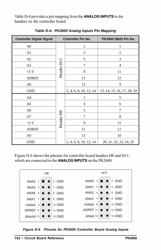
PK2600152 s Circuit Board Reference
Table D-4. PK2600 Analog Inputs Pin Mapping
Controller Digital Signal Controller Pin No. PK2600 DB25 Pin No.
A0 1 1
A1 3 2
A2 5 3
A3 7 4
+5 V 9 11
ADREF 11 12
A8 13 9
GND
Hea
der
H11
2, 4, 6, 8, 10, 12, 14 13, 14, 15, 16, 17, 18, 19
A4 1 5
A5 3 6
A6 5 7
A7 7 8
+5 V 9 11
ADREF 11 12
A9 13 10
GND
Hea
der
H8
2, 4, 6, 8, 10, 12, 14 20, 21, 22, 23, 24, 25
Table D-4 provides a pin mapping from the ANALOG INPUTS to theheaders on the controller board.
Figure D-6 shows the pinouts for controller board headers H8 and H11,which are connected to the ANALOG INPUTS on the PK2600.
Figure D-6. Pinouts for PK2600 Controller Board Analog Inputs
10
H8
1 2
3 4
5 6
7 8
9
ANA4
ANA5
ANA6
ANA7
+5ANA
GND
GND
GND
GND
GND
14
11 12
13
ADREF
ANAA9
GND
GND
10
H11
1 2
3 4
5 6
7 8
9
ANA0
ANA1
ANA2
ANA3
+5ANA
GND
GND
GND
GND
GND
14
11 12
13
ADREF
ANA8
GND
GND
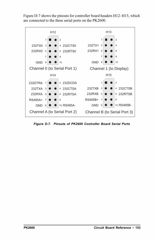
PK2600 Circuit Board Reference s 153
10
H12
1 2
3 4
5 6
7 8
9
232TX0
232RX0
GND
232CTS0
232RTS0
10
H14
1 2
3 4
5 6
7 8
9
232DTRA
232TXA
232RXA
RS485A+
GND
232DCDA
232CTSA
232RTSA
RS485A-
10
H13
1 2
3 4
5 6
7 8
9
232TX1
232RX1
GND
10
H15
1 2
3 4
5 6
7 8
9
232TXB
232RXB
RS485B+
GND
232CTSB
232RTSB
RS485B-
Channel 0 (to Serial Port 1) Channel 1 (to Display)
Channel A (to Serial Port 2) Channel B (to Serial Port 3)
Figure D-7 shows the pinouts for controller board headers H12H15, whichare connected to the three serial ports on the PK2600.
Figure D-7. Pinouts of PK2600 Controller Board Serial Ports
PK2600154 s Circuit Board Reference
Table D-5. Controller Board Jumper Settings
Header Pins DescriptionFactoryDefault
1–23–4
Connect for HVB00–HVB07 sinkingoutput
Connected
1–34–4
Connect for HVB00–HVB07 sourcingoutput
5–67–8
Connect for HVB08–HVB15 sinkingoutput
Connected
H3
5–76–8
Connect for HVB08–HVB15 sourcingoutput
1–3Connect for HVA0–HVA03 inputs pulledup
Connected
3–5Connect for HVA00–HVA03 inputspulled down
2–4Connect for HVA04–HVA07 inputspulled up
Connected
4–6Connect for HVA04–HVA07 inputspulled down
7–9Connect for HVA08–HVA15 inputspulled up
Connected
9–11Connect for HVA08–HVA15 inputspulled down
8–10Connect for 5-wire RS-232, DCD andDTR on Channel A
Connected
J2
10–12 Connect for 2-wire RS-485 on Channel A
1–23–4
Connect to enable RS-485 terminationresistors for Channel 1
Connected
5–6Connect for /INT0 serial communicationon Channel A and Channel B, disconnectto allow /INT0 for user application
ConnectedJ4
7–8Connect to allow /INT1 to be used as /ATon PLCBus, disconnect for /INT1 externaluse only
Connected
continued…
Jumper SettingsTable D-5 lists the jumper configurations for the configurable headers onthe controller board.
PK2600 Circuit Board Reference s 155
Table D-5. Controller Board Jumper Settings (concluded)
Header Pins DescriptionFactoryDefault
1–23–4
Connect to enable RS-485 terminationresistors for Channel A
Connected
J75–67–8
Connect to enable RS-485 terminationresistors for Channel B
Connected
1–3Connect to enable 5-wire RS-232 onChannel B
Connected
3–5Connect to enable 2-wire RS-485 forChannel B
Connected
2–4Connect to allow /DREQ0 to be used forChannel A
Connected
4–6Connect to allow /DREQ0 to be used forPWM, disconnect for user application
2, 4, 6Disconnected, /DREQ0 available for userapplication
7–9 Connect for 3-wire RS-232 on Channel 1 Connected
9–11 Connect for 2-wire RS-485 on Channel 1
10–12Connect to allow /DREQ1 to be used forChannel B
Connected
J8
8–10Connect to allow user application forChannel B

PK2600156 s Circuit Board Reference
(
Table D-6 lists the jumper settings for optional controller board configura-tions. These optional configurations involve adding or removing inputinterface or high-voltage driver ICs, which are surface-mounted. This workis most easily done in the factory in response to customer needs.
For ordering information, or for more details about thevarious options and prices, call your Z-World SalesRepresentative at (530) 757-3737.
Table D-6. Controller Board Jumper Setting for Optional Inputs/Outputs
Header Pins Description
Bank A Digital Outputs
1–23–4
Connect for HVA00–HVA07 sinking output
1–34–4
Connect for HVA00–HVA07 sourcing output
5–67–8
Connect for HVA08–HVA15 sinking output
H2
5–76–8
Connect for HVA08–HVA15 sourcing output
Bank B Digital Inputs
1–3 Connect for HVB0–HVB03 inputs pulled up
3–5 Connect for HVB00–HVB03 inputs pulled down
2–4 Connect for HVB04–HVB07 inputs pulled up
4–6 Connect for HVB04–HVB07 inputs pulled down
7–9 Connect for HVB08–HVB15 inputs pulled up
J3
9–11 Connect for HVB08–HVB15 inputs pulled down

PK2600 Circuit Board Reference s 157
Display BoardTable D-7 lists the header functions for the headers on the display board.Figure D-8 shows the header locations and the dimensions of the displayboard.
Figure D-8. Display Board Headers and Dimensions
Table D-7. Display Board Header Functions
Header Description
J1 LCD (hard-wired)
J2 Backlight
J3 LCD (ribbon cable)
J4 Programming port
J5 Touchscreen interface
J6 Keypad interface
J8 RS-232 port (header)
J11 DC power supply, RS-485 port
JP4
J11
R31
J6
J5
J2
J4
J1
JP1
J3
J9
JP3
J8
JP2
J7
0.25 typ(6.4)
6.400(163)
4.39
0(1
12)
0.2
typ
(5)
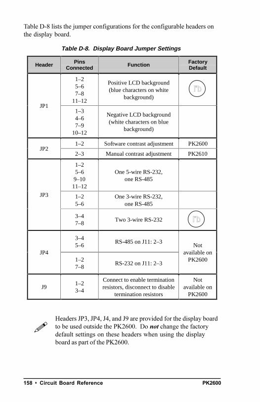
PK2600158 s Circuit Board Reference
Table D-8 lists the jumper configurations for the configurable headers onthe display board.
Headers JP3, JP4, J4, and J9 are provided for the display boardto be used outside the PK2600. Do not change the factorydefault settings on these headers when using the displayboard as part of the PK2600.
!
FD
Table D-8. Display Board Jumper Settings
Header PinsConnected Function Factory
Default
1–25–67–8
11–12
Positive LCD background(blue characters on white
background)
JP11–34–67–9
10–12
Negative LCD background(white characters on blue
background)
1–2 Software contrast adjustment PK2600JP2
2–3 Manual contrast adjustment PK2610
1–25–69–1011–12
One 5-wire RS-232,one RS-485
1–25–6
One 3-wire RS-232,one RS-485
JP3
3–47–8
Two 3-wire RS-232
3–45–6
RS-485 on J11: 2–3
JP41–27–8
RS-232 on J11: 2–3
Notavailable on
PK2600
J91–23–4
Connect to enable terminationresistors, disconnect to disable
termination resistors
Notavailable on
PK2600
FD
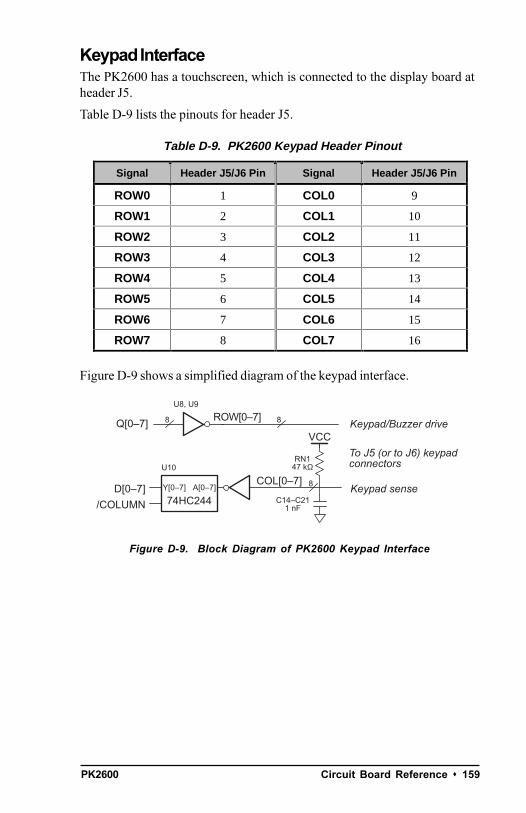
PK2600 Circuit Board Reference s 159
Keypad InterfaceThe PK2600 has a touchscreen, which is connected to the display board atheader J5.
Table D-9 lists the pinouts for header J5.
Figure D-9 shows a simplified diagram of the keypad interface.
Figure D-9. Block Diagram of PK2600 Keypad Interface
Table D-9. PK2600 Keypad Header Pinout
Signal Header J5/J6 Pin Signal Header J5/J6 Pin
ROW0 1 COL0 9
ROW1 2 COL1 10
ROW2 3 COL2 11
ROW3 4 COL3 12
ROW4 5 COL4 13
ROW5 6 COL5 14
ROW6 7 COL6 15
ROW7 8 COL7 16
U10
VCCQ[07]
ROW[07]
A[07]Y[07]
74HC244D[07]
/COLUMNKeypad sense
8
8
8
To J5 (or to J6) keypadconnectors
COL[07]
U8, U9
Keypad/Buzzer drive
C14C211 nF
RN147 kΩ

PK2600160 s Circuit Board Reference
Blank

PK2600 PLCBus s 161
APPENDIX E: PLCBUS
Appendix E provides the pin assignments for the PLCBus, describes theregisters, and lists the software drivers.
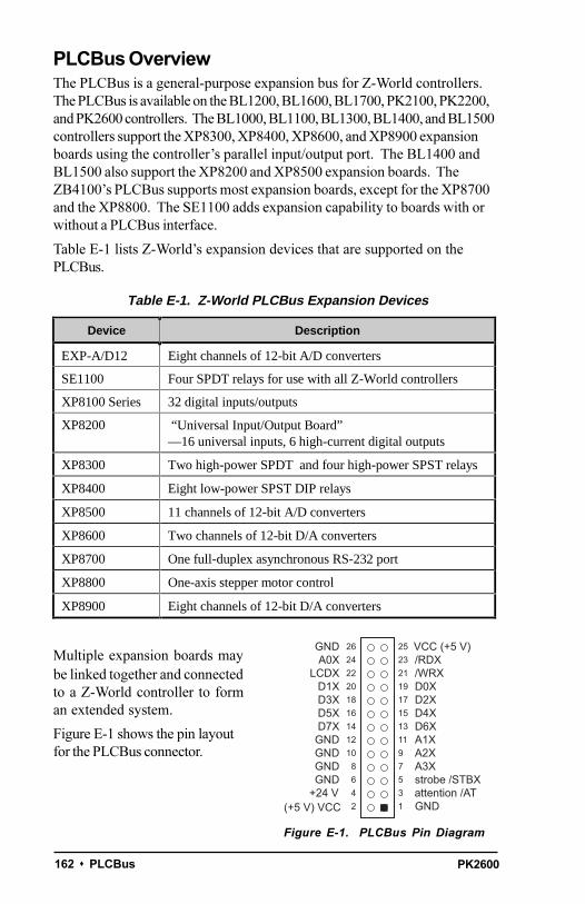
PK2600162 s PLCBus
PLCBus OverviewThe PLCBus is a general-purpose expansion bus for Z-World controllers.The PLCBus is available on the BL1200, BL1600, BL1700, PK2100, PK2200,and PK2600 controllers. The BL1000, BL1100, BL1300, BL1400, and BL1500controllers support the XP8300, XP8400, XP8600, and XP8900 expansionboards using the controllers parallel input/output port. The BL1400 andBL1500 also support the XP8200 and XP8500 expansion boards. TheZB4100s PLCBus supports most expansion boards, except for the XP8700and the XP8800. The SE1100 adds expansion capability to boards with orwithout a PLCBus interface.
Table E-1 lists Z-Worlds expansion devices that are supported on thePLCBus.
Multiple expansion boards maybe linked together and connectedto a Z-World controller to forman extended system.
Figure E-1 shows the pin layoutfor the PLCBus connector.
Table E-1. Z-World PLCBus Expansion Devices
Device Description
EXP-A/D12 Eight channels of 12-bit A/D converters
SE1100 Four SPDT relays for use with all Z-World controllers
XP8100 Series 32 digital inputs/outputs
XP8200 “Universal Input/Output Board”—16 universal inputs, 6 high-current digital outputs
XP8300 Two high-power SPDT and four high-power SPST relays
XP8400 Eight low-power SPST DIP relays
XP8500 11 channels of 12-bit A/D converters
XP8600 Two channels of 12-bit D/A converters
XP8700 One full-duplex asynchronous RS-232 port
XP8800 One-axis stepper motor control
XP8900 Eight channels of 12-bit D/A converters
24
13
6 58 7
10 912 1114 1316 1518 1720 1922 2124 2326 25
GNDD7XD5XD3XD1X
LCDXA0X
GND
GND attention /ATstrobe /STBXGNDA3XGNDA2XGNDA1X
/RDXVCC (+5 V)
D0X/WRX
D4XD2X
D6X
+24 V(+5 V) VCC
Figure E-1. PLCBus Pin Diagram
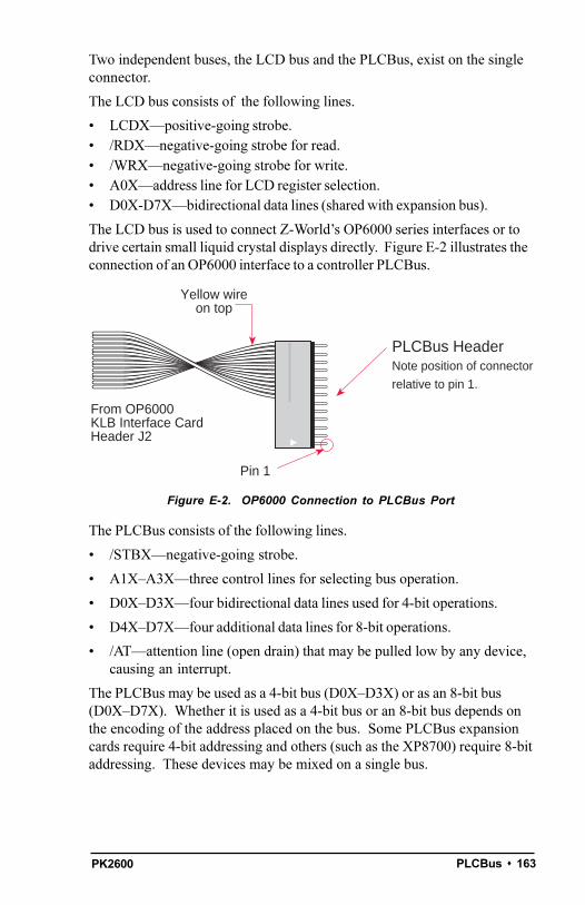
PK2600 PLCBus s 163
Two independent buses, the LCD bus and the PLCBus, exist on the singleconnector.
The LCD bus consists of the following lines.
LCDXpositive-going strobe. /RDXnegative-going strobe for read. /WRXnegative-going strobe for write. A0Xaddress line for LCD register selection. D0X-D7Xbidirectional data lines (shared with expansion bus).
The LCD bus is used to connect Z-Worlds OP6000 series interfaces or todrive certain small liquid crystal displays directly. Figure E-2 illustrates theconnection of an OP6000 interface to a controller PLCBus.
Figure E-2. OP6000 Connection to PLCBus Port
The PLCBus consists of the following lines.
/STBXnegative-going strobe.
A1XA3Xthree control lines for selecting bus operation.
D0XD3Xfour bidirectional data lines used for 4-bit operations.
D4XD7Xfour additional data lines for 8-bit operations.
/ATattention line (open drain) that may be pulled low by any device,causing an interrupt.
The PLCBus may be used as a 4-bit bus (D0XD3X) or as an 8-bit bus(D0XD7X). Whether it is used as a 4-bit bus or an 8-bit bus depends onthe encoding of the address placed on the bus. Some PLCBus expansioncards require 4-bit addressing and others (such as the XP8700) require 8-bitaddressing. These devices may be mixed on a single bus.
Yellow wireon top
PLCBus HeaderNote position of connector
relative to pin 1.
From OP6000KLB Interface CardHeader J2
Pin 1

PK2600164 s PLCBus
There are eight registers corresponding to the modes determined by buslines A1X, A2X, and A3X. The registers are listed in Table E-2.
Writing or reading one of these registers takes care of all the bus details.Functions are available in Z-Worlds software libraries to read from or writeto expansion bus devices.
To communicate with a device on the expansion bus, first select a registerassociated with the device. Then read or write from/to the register. Theregister is selected by placing its address on the bus. Each devicerecognizes its own address and latches itself internally.
A typical device has three internal latches corresponding to the threeaddress bytes. The first is latched when a matching BUSADR0 is detected.The second is latched when the first is latched and a matching BUSADR1is detected. The third is latched if the first two are latched and a matchingBUSADR2 is detected. If 4-bit addressing is used, then there are three 4-bit address nibbles, giving 12-bit addresses. In addition, a special registeraddress is reserved for address expansion. This address, if ever used,would provide an additional four bits of addressing when using the 4-bitconvention.
If eight data lines are used, then the addressing possibilities of the busbecome much greatermore than 256 million addresses according to theconventions established for the bus.
Table E-2. PLCBus Registers
Register Address A3 A2 A1 Meaning
BUSRD0 C0 0 0 0 Read data, one way
BUSRD1 C2 0 0 1Read data, anotherway
BUSRD2 C4 0 1 0 Spare, or read data
BUSRESET C6 0 1 1Read this register toreset the PLCBus
BUSADR0 C8 1 0 0First address nibbleor byte
BUSADR1 CA 1 0 1Second addressnibble or byte
BUSADR2 CC 1 1 0Third address nibbleor byte
BUSWR CE 1 1 1 Write data
PK2600 PLCBus s 165
Place an address on the bus by writing (bytes) to BUSADR0, BUSADR1and BUSADR2 in succession. Since 4-bit and 8-bit addressing modes mustcoexist, the lower four bits of the first address byte (written to BUSADR0)identify addressing categories, and distinguish 4-bit and 8-bit modes fromeach other.
There are 16 address categories, as listed in Table E-3. An x indicatesthat the address bit may be a 1 or a 0.
This scheme uses less than the full addressing space. The mode notationindicates how many bus address cycles must take place and how many bitsare placed on the bus during each cycle. For example, the 5 × 3 modemeans three bus cycles with five address bits each time to yield 15-bitaddresses, not 24-bit addresses, since the bus uses only the lower five bitsof the three address bytes.
Table E-3. First-Level PLCBus Address Coding
First Byte Mode Addresses Full Address Encoding
– – – – 0 0 0 0– – – – 0 0 0 1– – – – 0 0 1 0– – – – 0 0 1 1
4 bits × 3 256256256256
0000 xxxx xxxx0001 xxxx xxxx0010 xxxx xxxx0011 xxxx xxxx
– – – x 0 1 0 0– – – x 0 1 0 1– – – x 0 1 1 0– – – x 0 1 1 1
5 bits × 3 2,0482,0482,0482,048
x0100 xxxxx xxxxxx0101 xxxxx xxxxxx0110 xxxxx xxxxxx0111 xxxxx xxxxx
– – x x 1 0 0 0– – x x 1 0 0 1
6 bits × 3 16,38416,384
xx1000 xxxxxx xxxxxxxx1001 xxxxxx xxxxxx
– – x x 1 0 1 0 6 bits × 1 4 xx1010
– – – – 1 0 1 1 4 bits × 1 1 1011 (expansion register)
x x x x 1 1 0 0 8 bits × 2 4,096 xxxx1100 xxxxxxxx
x x x x 1 1 0 1 8 bits × 3 1M xxxx1101 xxxxxxxx xxxxxxxx
x x x x 1 1 1 0 8 bits × 1 16 xxxx1110
x x x x 1 1 1 1 8 bits × 1 16 xxxx1111

PK2600166 s PLCBus
Z-World provides software drivers that access the PLCBus. To allowaccess to bus devices in a multiprocessing environment, the expansionregister and the address registers are shadowed with memory locationsknown as shadow registers. The 4-byte shadow registers, which are savedat predefined memory addresses, are as follows.
Before the new addresses or expansion register values are output to thebus, their values are stored in the shadow registers. All interrupts that usethe bus save the four shadow registers on the stack. Then, when exitingthe interrupt routine, they restore the shadow registers and output thethree address registers and the expansion registers to the bus. This allowsan interrupt routine to access the bus without disturbing the activity of abackground routine that also accesses the bus.
To work reliably, bus devices must be designed according to the following rules.
1. The device must not rely on critical timing such as a minimum delaybetween two successive register accesses.
2. The device must be capable of being selected and deselected withoutadversely affecting the internal operation of the controller.
Allocation of Devices on the Bus
4-Bit DevicesTable E-4 provides the address allocations for the registers of 4-bit devices.
SHBUS1 SHBUS1+1SHBUS0 SHBUS0+1 SHBUS0+2 SHBUS0+3
Bus expansion BUSADR0 BUSADR1 BUSADR2
Table E-4. Allocation of Registers
A1 A2 A3 Meaning
000j 000j xxxjdigital output registers, 64 registers64 × 8 = 512 1-bit registers
000j 001j xxxj analog output modules, 64 registers
000j 01xj xxxjdigital input registers, 128 registers128 × 4 = 512 input bits
000j 10xj xxxj analog input modules, 128 registers
000j 11xj xxxj 128 spare registers (customer)
001j xxxj xxxj 512 spare registers (Z-World)
j controlled by board jumperx controlled by PAL

PK2600 PLCBus s 167
Digital output devices, such as relay drivers, should be addressed withthree 4-bit addresses followed by a 4-bit data write to the control register.The control registers are configured as follows
bit 3 bit 2 bit 1 bit 0A2 A1 A0 D
The three address lines determine which output bit is to be written. Theoutput is set as either 1 or 0, according to D. If the device exists on thebus, reading the register drives bit 0 low. Otherwise bit 0 is a 1.
For digital input, each register (BUSRD0) returns four bits. The readregister, BUSRD1, drives bit 0 low if the device exists on the bus.
8-Bit DevicesZ-Worlds XP8700 and XP8800 expansion boards use 8-bit addressing.Refer to the XP8700 and XP8800 manual.
Expansion Bus SoftwareThe expansion bus provides a convenient way to interface Z-Worldscontrollers with expansion boards or other specially designed boards. Theexpansion bus may be accessed by using input functions. Follow thesuggested protocol. The software drivers are easier to use, but are lessefficient in some cases. Table E-5 lists the libraries.
Table E-5. Dynamic C PLCBus Libraries
Library Needed Controller
DRIVERS.LIB All controllers
EZIOTGPL.LIB BL1000
EZIOLGPL.LIB BL1100
EZIOMGPL.LIB BL1400, BL1500
EZIOPLC.LIB BL1200, BL1600, PK2100, PK2200, ZB4100
EZIOPLC2.LIB BL1700, PK2600
PBUS_TG.LIB BL1000
PBUS_LG.LIB BL1100, BL1300
PLC_EXP.LIB BL1200, BL1600, PK2100, PK2200

PK2600168 s PLCBus
There are 4-bit and 8-bit drivers. The 4-bit drivers employ the followingcalls.
void eioResetPlcBus()
Resets all expansion boards on the PLCBus. When using this call,make sure there is sufficient delay between this call and the first accessto an expansion board.
LIBRARY: EZIOPLC.LIB, EZIOPLC2.LIB, EZIOMGPL.LIB.
void eioPlcAdr12( unsigned addr )
Specifies the address to be written to the PLCBus using cyclesBUSADR0, BUSADR1, and BUSADR2.
PARAMETER: addr is broken into three nibbles, and one nibble iswritten in each BUSADRx cycle.
LIBRARY: EZIOPLC.LIB, EZIOPLC2.LIB, EZIOMGPL.LIB.
void set16adr( int adr )
Sets the current address for the PLCBus. All read and write operationsaccess this address until a new address is set.
PARAMETER: adr is a 16-bit physical address. The high-order nibblecontains the value for the expansion register, and the remaining three 4-bit nibbles form a 12-bit address (the first and last nibbles must beswapped).
LIBRARY: DRIVERS.LIB.
void set12adr( int adr )
Sets the current address for the PLCBus. All read and write operationsaccess this address until a new address is set.
PARAMETER: adr is a 12-bit physical address (three 4-bit nibbles)with the first and third nibbles swapped.
LIBRARY: DRIVERS.LIB.
void eioPlcAdr4( unsigned addr )
Specifies the address to be written to the PLCBus using only cycleBUSADR2.
PARAMETER: addr is the nibble corresponding to BUSADR2.
LIBRARY: EZIOPLC.LIB, EZIOPLC2.LIB, EZIOMGPL.LIB.
PK2600 PLCBus s 169
void set4adr( int adr )
Sets the current address for the PLCBus. All read and write operationsaccess this address until a new address is set.
A 12-bit address may be passed to this function, but only the last fourbits will be set. Call this function only if the first eight bits of theaddress are the same as the address in the previous call to set12adr.
PARAMETER: adr contains the last four bits (bits 811) of thephysical address.
LIBRARY: DRIVERS.LIB.
char _eioReadD0( )
Reads the data on the PLCBus in the BUSADR0 cycle.
RETURN VALUE: the byte read on the PLCBus in the BUSADR0 cycle.
LIBRARY: EZIOPLC.LIB, EZIOPLC2.LIB, EZIOMGPL.LIB.
char _eioReadD1( )
Reads the data on the PLCBus in the BUSADR1 cycle.
RETURN VALUE: the byte read on the PLCBus in the BUSADR1 cycle.
LIBRARY: EZIOPLC.LIB, EZIOPLC2.LIB, EZIOMGPL.LIB.
char _eioReadD2( )
Reads the data on the PLCBus in the BUSADR2 cycle.
RETURN VALUE: the byte read on the PLCBus in the BUSADR2 cycle.
LIBRARY: EZIOPLC.LIB, EZIOPLC2.LIB, EZIOMGPL.LIB.
char read12data( int adr )
Sets the current PLCBus address using the 12-bit adr, then reads fourbits of data from the PLCBus with BUSADR0 cycle.
RETURN VALUE: PLCBus data in the lower four bits; the upper bitsare undefined.
LIBRARY: DRIVERS.LIB.
PK2600170 s PLCBus
char read4data( int adr )
Sets the last four bits of the current PLCBus address using adr bits 811, then reads four bits of data from the bus with BUSADR0 cycle.
PARAMETER: adr bits 811 specifies the address to read.
RETURN VALUE: PLCBus data in the lower four bits; the upper bitsare undefined.
LIBRARY: DRIVERS.LIB.
void _eioWriteWR( char ch)
Writes information to the PLCBus during the BUSWR cycle.
PARAMETER: ch is the character to be written to the PLCBus.
LIBRARY: EZIOPLC.LIB, EZIOPLC2.LIB, EZIOMGPL.LIB.
void write12data( int adr, char dat )
Sets the current PLCBus address, then writes four bits of data to thePLCBus.
PARAMETER: adr is the 12-bit address to which the PLCBus is set.
dat (bits 03) specifies the data to write to the PLCBus.
LIBRARY: DRIVERS.LIB.
void write4data( int address, char data )
Sets the last four bits of the current PLCBus address, then writes fourbits of data to the PLCBus.
PARAMETER: adr contains the last four bits of the physical address(bits 811).
dat (bits 03) specifies the data to write to the PLCBus.
LIBRARY: DRIVERS.LIB.
The 8-bit drivers employ the following calls.
void set24adr( long address )
Sets a 24-bit address (three 8-bit nibbles) on the PLCBus. All read andwrite operations will access this address until a new address is set.
PARAMETER: address is a 24-bit physical address (for 8-bit bus)with the first and third bytes swapped (low byte most significant).
LIBRARY: DRIVERS.LIB.
PK2600 PLCBus s 171
void set8adr( long address )
Sets the current address on the PLCBus. All read and write operationswill access this address until a new address is set.
PARAMETER: address contains the last eight bits of the physicaladdress in bits 1623. A 24-bit address may be passed to this function,but only the last eight bits will be set. Call this function only if the first16 bits of the address are the same as the address in the previous call toset24adr.
LIBRARY: DRIVERS.LIB.
int read24data0( long address )
Sets the current PLCBus address using the 24-bit address, then readseight bits of data from the PLCBus with a BUSRD0 cycle.
RETURN VALUE: PLCBus data in lower eight bits (upper bits 0).
LIBRARY: DRIVERS.LIB.
int read8data0( long address )
Sets the last eight bits of the current PLCBus address using addressbits 1623, then reads eight bits of data from the PLCBus with aBUSRD0 cycle.
PARAMETER: address bits 1623 are read.
RETURN VALUE: PLCBus data in lower eight bits (upper bits 0).
LIBRARY: DRIVERS.LIB.
void write24data( long address, char data )
Sets the current PLCBus address using the 24-bit address, then writeseight bits of data to the PLCBus.
PARAMETERS: address is 24-bit address to write to.
data is data to write to the PLCBus.
LIBRARY: DRIVERS.LIB.
void write8data( long address, char data )
Sets the last eight bits of the current PLCBus address using addressbits 1623, then writes eight bits of data to the PLCBus.
PARAMETERS: address bits 1623 are the address of the PLCBus towrite.
data is data to write to the PLCBus.
LIBRARY: DRIVERS.LIB.

PK2600172 s PLCBus
Blank
PK2600 Serial Interface Board 2 s 173
APPENDIX F:
SERIAL INTERFACE BOARD 2
Appendix F provides technical details and baud rate configuration data forZ-Worlds SIB2. The following sections are included.
Introduction
Dimensions

174 s Serial Interface Board 2 PK2600
IntroductionThe SIB2 is an interface adapter used to program the PK2600. The SIB2 iscontained in an ABS plastic enclosure, making it rugged and reliable. TheSIB2 enables both the controller board and the display board to communi-cate with Dynamic C via the Z180s clocked serial I/O (CSI/O) port, freeingthe serial ports for use by the application during programming anddebugging.
The SIB2s 8-pin cable plugs into the target PK2600s processor through anaperture in the backplate, and a 6-conductor RJ-12 phone cable connectsthe SIB2 to the host PC. The SIB2 automatically selects its baud rate tomatch the communication rates established by the host PC (9600, 19,200, or57,600 bps). However, the SIB2 determines the hosts communication baudrate only on the first communication after reset. To change baud rates,change the COM baud rate, reset the target PK2600 board (which alsoresets the SIB2), then select Reset Target from Dynamic C.
Chapter 2 provides detailed information on connecting theSIB2 to the PK2600.
The SIB2 receives power and resets from the target board on the PK2600via the 8-pin connector J1. Therefore, do not unplug the SIB2 from thePK2600 while power is applied. To do so could damage both the PK2600and the SIB2; additionally, the target may reset.
Never connect or disconnect the SIB2 with power applied tothe controller.
The SIB2 consumes approximately 60 mA from the +5 V supply. The target-system current consumption therefore increases by this amount while theSIB2 is connected to the PK2600.
$
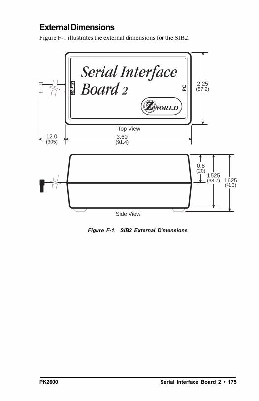
PK2600 Serial Interface Board 2 s 175
External DimensionsFigure F-1 illustrates the external dimensions for the SIB2.
Figure F-1. SIB2 External Dimensions
Top View
Side View
2.25(57.2)
12.0(305)
3.60(91.4)
0.8(20)
1.525(38.7) 1.625
(41.3)

176 s Serial Interface Board 2 PK2600
Blank
PK2600 Advanced Topics s 177
APPENDIX G: ADVANCED TOPICS
Appendix G provides more advanced information to help the user needingto implement special applications. The following topics are included.
Power Management
Simulated EEPROM
Pulse-Width Modulation Software
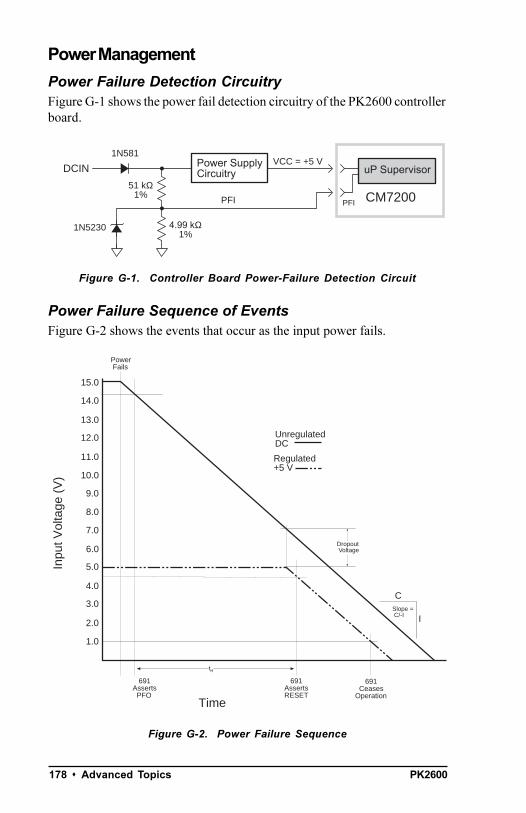
PK2600178 s Advanced Topics
Power Management
Power Failure Detection CircuitryFigure G-1 shows the power fail detection circuitry of the PK2600 controllerboard.
Figure G-1. Controller Board Power-Failure Detection Circuit
Power Failure Sequence of EventsFigure G-2 shows the events that occur as the input power fails.
Figure G-2. Power Failure Sequence
1N581
1N5230
DCIN
CM7200PFI
Power SupplyCircuitry uP Supervisor
4.99 kΩ1%
51 kΩ1%
PFI
VCC = +5 V
1.0
2.0
9.0
8.0
7.0
6.0
5.0
4.0
3.0
I
UnregulatedDC
Regulated+5 V
691Asserts PFO
691AssertsRESET
691 CeasesOperation
tH
Power Fails
Time
CSlope = C/-I
Dropout Voltage
10.0
11.0
14.0
13.0
12.0
15.0
Inpu
t Vol
tage
(V
)

PK2600 Advanced Topics s 179
1. The power-management IC triggers a power-fail /NMI (nonmaskableinterrupt) when the DC input voltage falls within the range of 14.44 V to14.72 V DC.
2. At some point, the raw input voltage will not be sufficient for theregulator to provide 5 V DC to the controller board due to dropoutvoltage. At that point the regulated output begins to drop. The power-management IC triggers a reset when the regulated 5 V DC output fallswithin the range of 4.50 V to 4.75 V DC. This causes the power-failroutine to be invoked. The power-fail routine can be used to storeimportant state data.
Use a power supply with a large capacitance if you need toincrease the holdup time. This will provide additional time forthe controller board to execute a safe shutdown.
3. The power management IC switches power for the time/date clock andSRAM to the lithium backup battery when the regulated voltage fallsbelow the battery voltage of approximately 3 V DC.
4. The 691 power management IC keeps the system in reset until theregulated voltage drops below 1 V DC. At this point the power-management IC ceases operating. By this time, the portion of thecircuitry not battery-backed has already ceased functioning.
The ratio of your power supplys output capacitors value to your circuitscurrent draw determines the actual holdup time.
A situation similar to a continuous low input (brownout) can occur if thepower supply is overloaded. For example, when a high-current device suchas a relay turns ON, the raw voltage supplied to the PK2600 may dip below14.44 V DC. The interrupt routine performs a shutdown. This shutdownturns off the relay, clearing the problem. However, if the cause of theoverload persists, the system oscillates, alternately experiencing anoverload and then resetting. Using a power supply with a sufficiently largecurrent capacity will correct this problem.
If you remove the power cable abruptly from the controller board side, thenonly the capacitors on the board provide power, reducing computing timeto a few microseconds. These times can vary considerably depending onsystem configuration and loads on the controller board power supplies.
The interval between the power-failure detection and entry to the power-failure interrupt routine is approximately 100 µs, or less if Dynamic C /NMIcommunication is not in use.
Tip
PK2600180 s Advanced Topics
Simulated EEPROMThe PK2600 uses a section of the flash EPROM on the controller board tosimulate EEPROM. The size of the simulated EEPROM is 512 bytes (notKbytes). Locations 0x02 through 0x3D are used to store the analog inputcalibration constants. The rest of the simulated EEPROM is free for use bythe application. These functions are used to read/write from/to thesimulated EEPROM.
int ee_rd( int address )
Reads and returns data from flash EPROM storage location address.The function returns 1 if it is unable to read data.
LIBRARY: BIOS.LIB
int ee_wr( int address, int data )
Writes data to flash EPROM storage location address. The functionreturns 1 if it is unable to write data.
LIBRARY: BIOS.LIB
Locations 0x02 through 0x3D on the display board are reserved for asimulated EEPROM, but are not presently used.

PK2600 Advanced Topics s 181
Pulse-Width Modulation (PWM) Software
PWM Addressing DetailThe driver of the PWM on the PK2600 controller board is fairly compli-cated. This is because it uses the clock output from communication port 1(CKA1) to drive the request line DMA Channel 0 in edge detection mode.The simple interface previously described in Chapter 4 provides PWMsupport for output 0 to output 3. If the application requires more PWMchannels or require specific frequencies or precision, the applicationengineer may need to make trade-offs.
This section describes how PWM channels are driven, as well as how tocustomize PWM resource allocation to compromise number of modulatedchannels, frequency, and resolution.
1. Determine the number of channels, frequency, and resolution.
A pulse-width modulated waveform has a frequency and a resolution. Thefrequency states how many times the pattern repeats itself in a second(Hz). The resolution states how many divisions within one waveform canbe resolved (distinguished). As a collection, the PWM driver also needs toknow the total number of channels to be pulse-width modulated. Thecalculations in this section are made with the assumption that all channelshave the same frequency and resolution.
The clock output from communication port 1 (CKA1) must have a fre-quency,
f1 = N
ch × f
w × R
w ,
where which f1 is the frequency of CKA1, N
ch is the number of channels
PW modulated, fw is the frequency of each channel, and R
w is the resolu-
tion in number of divisions per wave.
For example, the driver interface, _eioSetupAO1st, makes the followingassumptions.
Nch
= 4
f1 = 76,800 Hz
Rw = 256
Consequently, fw = 76,800 Hz/(4 × 256) = 75 Hz.
2. Declare storage for the WPB (waveform pattern buffer).
Memory must be allocated to store the waveform pattern.
PK2600182 s Advanced Topics
3. Set up the waveform.
The PWM functions use the Z180s built-in DMA mechanism to transferPWM edges from memory to the high-current ports at specific timeintervals. Each edge is a byte whose least-significant four bits select oneof the high-current outputs, output 0 through output 6. The least signifi-cant bit is a 1 to turn the specified port on (rising PWM edge) or a 0 toturn the specified port off (falling PWM edge). Edges for the channelsbeing pulse-width modulated are then grouped into composite transitions.
Each composite transition is a series of edges, each representing onepossible transition for an individual channel. For example, if output 0 andoutput 1 are the only pulse-width modulated channels, a compositetransition consists of two bytes. The first byte specifies a possibletransition for channel output 0. The second byte specifies a possibletransition for channel output 1.
Let us assume the first byte in the composite transition corresponds tooutput 0, and the second byte corresponds to output 1.
The composite PWM waveform is a series of composite transitions (CTs)that specify the duty cycle of the pulse-width modulated channels. Forexample, if output 0 is to have a 0.375 duty cycle, output 1 is to be at 0.75duty cycle, and the resolution is 8 divisions per cycle, a simple wave formwould be as follows.
CT1: turn on output 0, turn on output 1.
CT2: do nothing.
CT3: do nothing.
CT4: turn off output 0.
CT5: do nothing.
CT6: do nothing.
CT7: turn off output 1.
CT8: do nothing.
Go back to CT1.
PK2600 Advanced Topics s 183
Outputting the byte 0x01 turns on output 0, 0x00 turns off output 0, 0x03turns on output 1, and 0x02 turns off output 1. The byte 0x0E is an no-op and it does nothing. The composite transitions (with no-ops) can betranslated into the following byte sequence to be sent to the I/O address0x4100.
CT1: 0x01, 0x03
CT2: 0x0E, 0x0E
CT3: 0x0E, 0x0E
CT4: 0x00, 0x0E
CT5: 0x0E, 0x0E
CT6: 0x0E, 0x0E
CT7: 0x0E, 0x02
CT8: 0x0E, 0x0E
Go back to CT1
The equivalent byte stream (contents in the waveform pattern buffer) is arepeating pattern of the following.
0x01, 0x03, 0x0E, 0x0E, 0x0E, 0x0E, 0x00, 0x0E,0x0E, 0x0E, 0x0E, 0x0E, 0x0E, 0x02, 0x0E, 0x0E
The driver library provides a function, dmapwmSetBuf, that allows theapplication engineer to modify the content of the waveform pattern buffer.
4. Set up the clock.
The DMA device transfer from memory to I/O port address 0x4100 is drivenby falling edges on signal /DREQ0. Since /DREQ0 is connected to CKA1(the clock output of communication channel 1), the communication speedof communication channel 1 determines how frequently the DMA devicetransfer memory to I/O. Each transfer corresponds to one edge in theprevious section.
Refer to the Zilog users manual for more information on howto set up the CKA1 frequency for the Z80180/Z180 or to theHitachi users manual for the 64180 MPU.
The driver does include a function, dmapwmInit, that sets up the fre-quency of CKA1. The function is described later in this appendix.
The PWM interface sets up CKA1 to clock at 76,800 Hz in the call_eioSetupAO1st().
$
PK2600184 s Advanced Topics
5. Refresh the DMA counter and source address.
The DMA device does not automatically reload the counter and sourceaddress registers when the specified amount of bytes is transferred. Whenthe DMA device finishes transferring the specified amount of bytes, itstops and optionally causes an interrupt. In other words, the PWMwaveform is abruptly ended when the DMA finishes.
To overcome this limitation, the application program must periodicallyrefresh the counter and source address registers of the DMA device.The refresh should check whether the counter is less than a critical number.If so, both the counter and the source address registers must be re-wound to a previous state (a larger counter value and a correspondinglower source address).
Note that the PWM waveforms cannot be disrupted while it is refreshingthe registers. In other words, the previous state to which the refreshroutine restores must be phase synchronized with the PWM waveforms atthe moment.
The driver library provides a refresh routine, _eioBrdAORf, to refresh theDMA counter and source address registers. _eioBrdAORf() can becalled from a preemptive task or from the main program. The refreshroutine must be called frequently enough so that the DMA counter neverreaches 0. The following inequality states the requirement.
fr ≥ f
1/(l
wpb/2)
in which fr is the refresh frequency, f
1 is the frequency of CKA1, and l
wpb is
the total length of the waveform pattern buffer.
For example, _eioSetupAO1st() sets up f1 = 76,800 Hz and l
wpb = 4096.
As a result, the application engineer must ensure fr ≥ 37.5 Hz.
6. Changing duty cycles.
Once the PWM waveforms are up and running, the application may needto change the duty cycles for the channel(s). This poses two problems.First, the change should only be done to the channel that needs a changeof duty cycle, all other channels should remain the same. Second, thechange must become effective phase synchronized with the currentwaveform.
The solution to the first problem depends on how the edges are repre-sented. In particular, it depends on whether the no-op edges are used. Ifthe no-op edges are used, changing duty cycle is a matter of moving theedges that are not no-op. For example, in our example in the set up the
PK2600 Advanced Topics s 185
waveform section, if we wish to change the duty cycle of output 0 to 0.25,we change the waveform from
0x01, 0x03, 0x0E, 0x0E, 0x0E, 0x0E, 0x00, 0x0E,0x0E, 0x0E, 0x0E, 0x0E, 0x0E, 0x02, 0x0E, 0x0E
to
0x01, 0x03, 0x0E, 0x0E, 0x00, 0x0E, 0x0E, 0x0E,0x0E, 0x0E, 0x0E, 0x0E, 0x0E, 0x02, 0x0E, 0x0E
The underlined edges are the only ones affected.
Of course, the waveform pattern buffer may have the pattern repeatedmany times. Each occurrence of the pattern in the buffer must be modifiedin the same manner.
However, although the use of no-op edges seems to be compute-timeinexpensive, it does require the application to maintain the location of thenon-no-op edges. In other words, besides the waveform pattern buffer, theapplication program must maintain a duty cycle variable for each channel.
Recall that the second problem of changing the duty cycle is the require-ment for the change to be phase synchronized to the current waveform.Many of the involved issues are similar to those of refreshing the DMAcounter and pointer. The driver software library provides the functiondmapwmSwBuf to switch waveform pattern buffers.
PWM SoftwareThe functions shown below are second level functions that allow morePWM outputs. They are also more complex and require a morein-depth understanding of PWM and DMA generation. These functionsare located in EZIODPWM.LIB.
void dmapwmSetBuf ( char *pBufStart,char bufLength256,unsigned step, char outChar )
Formats part of the waveform pattern buffer for DMA-driven PWM.
In other words, dmapwmSetBuf does the following: starting at theaddress pointed to by pBufStart, for bufLength256 many 256-bytepages, change every step bytes to outChar.
PARAMETERS: pBufStart points to the first byte to be formatted.Note that pBufStart does not always have to point to a 256-bytealigned address.
bufLength256 is the length of the buffer, including the overflow area.
step is the number of bytes to skip between outputting outChar.
outChar is the actual bytes to send to the I/O address.

PK2600186 s Advanced Topics
void dmapwmSwBuf ( unsigned newBuf256 )
In order to facilitate all-or-none duty cycle transitions, you should usetwo buffers. While one buffer is being used by the DMA mechanism togenerate the PWM output, modify the other buffer for the new PWMpattern. When the new buffer is ready, this function should be calledto switch to use the buffer at the address pointed to by newBuf256 in256-byte units.
char *dmapwmBufBeg ( char *bufPtr )
The buffer used by the PWM mechanism starts at 256-byte boundaries.Normal data definition declarations such as
char buffer[0x2000]
start at byte boundaries. dmapwmBufBeg returns a character pointerthat points to the first 256-byte aligned root address larger than orequal to the parameter bufPtr.
void dmapwmInit( unsigned phyBuffer256,unsigned bufSize256, unsigned resSize256,unsigned ioAddr, char cka1rate )
Initializes the DMA PWM mechanism.
When the function returns, CKA1 of communication port 1 generatesclock pulses at cka1rate * 19.2 kHz to /DREQ0. DMA Channel 0would then perform memory to I/O transfer for each clock pulse fallingedge.
PARAMETERS: phyBuffer256 is the 256 byte aligned physicaladdress of the buffer in 256-byte units. In general, if the buffer isdefined as an array in root memory (that is, of type (char *)), thefollowing expression should be passed to this parameter
(unsigned)((xmadr(buffer)+255)>>8)
in which buffer is a pointer of type (char *) to the array.
bufsize256 is the size of the buffer, in 256 byte units. This sizeshould not include the overflow area.
resSize256 is the size of the overflow area in 256 byte units.
ioAddr is the port to which the DMA should transfer memory content.
cka1rate is the clock rate generated by CKA1 in 19.2 kHz units.Allowed numbers are 2, 4, and 8.

PK2600 Advanced Topics s 187
Sample ProgramBL17PWM1.C and BL17PWM2.C are sample programs which show how touse the pulse width modulation feature using the functions listed above.They can be found in the Dynamic C SAMPLES\BL17XX directory.
The PWM functions use the Z180s built-in DMA hardware.Using this DMA-driven PWM limits the communicationspeed of the Z180s Serial Port 1 to 4800 bps, and the Z180runs effectively at least 8% slower. In addition you mustensure your application calls _eioBrdAORf at least every25 ms to refresh the drivers period.
If necessary, call Z-World Technical Support at(530)757-3737 for assistance.

PK2600188 s Advanced Topics
Blank

PK2600 Battery s 189
APPENDIX H: BATTERY
Appendix H provides information about the onboard lithium backupbatteries.

PK2600190 s Battery
Battery Life and Storage ConditionsThe batteries on the PK2600 controller board and display board willprovide approximately 9,000 h of backup time for the onboard real-timeclock and static RAM. However, backup time longevity is affected bymany factors, including the amount of time the PK2600 is unpowered andthe static RAM size. Most systems are operated on a continuous basis,with the battery supplying power to the real-time clock and the static RAMduring power outages and/or during routine maintenance. The timeestimate reflects the shelf life of a lithium ion battery with occasional userather than the ability of the battery to power the circuitry full time.
The battery on the controller board has a capacity of 190 mA·h. At 25°C, thereal-time clock draws 3 µA when idle, and the 32K SRAM draws 2 µA. If thePK2600 were unpowered 100 percent of the time, the battery would last38,000 hours (4.3 years).
The battery on the display board has a capacity of 165 mA·h. At 25°C, thereal-time clock draws 3 µA when idle, and the 128K SRAM draws 4 µA. Ifthe PK2600 were unpowered 100 percent of the time, the battery would last23,570 hours (2.7 years).
To maximize the battery life, the PK2600 should be stored at room tempera-ture in the factory packaging until field installation. Take care that thePK2600 is not exposed to extreme temperature, humidity, and/or contami-nants such as dust and chemicals.
To ensure maximum battery shelf life, follow proper storage procedures.Replacement batteries should be kept sealed in the factory packaging atroom temperature until installation. Protection against environmentalextremes will help maximize battery life.
Replacing Soldered Lithium BatteryUse the following steps to replace the battery.
1. Locate the three pins on the bottom side of the printed circuit boardthat secure the battery to the board.
2. Carefully de-solder the pins and remove the battery. Use a soldersucker to clean up the holes.
3. Install the new battery and solder it to the board. Use only a PanasonicBR2325-1HG or its equivalent for the controller board, and a RenataCR2325RH or its equivalent for the display board.
PK2600 Battery s 191
Battery Cautions Caution (English)
There is a danger of explosion if the battery is incorrectly replaced.Replace only with the same or equivalent type recommended by themanufacturer. Dispose of used batteries according to the manufactur-ers instructions.
Warnung (German)
Explosionsgefahr durch falsches Einsetzen oder Behandein der Batterie.Nur durch gleichen Typ oder vom Hersteller empfohlenen Ersatztypersetzen. Entsorgung der gebrauchten Batterien gemäb denAnweisungen des Herstellers.
Attention (French)
Il y a danger dexplosion si la remplacement de la batterie est incorrect.Remplacez uniquement avec une batterie du même type ou dun typeéquivalent recommandé par le fabricant. Mettez au rebut les batteriesusagées conformément aux instructions du fabricant.
Cuidado (Spanish)
Peligro de explosión si la pila es instalada incorrectamente. Reemplacesolamente con una similar o de tipo equivalente a la que el fabricanterecomienda. Deshagase de las pilas usadas de acuerdo con lasinstrucciones del fabricante.
Waarschuwing (Dutch)
Explosiegevaar indien de batterij niet goed wordt vervagen.Vervanging alleen door een zelfde of equivalent type als aanbevolendoor de fabrikant. Gebruikte batterijen afvoeren als door de fabrikantwordt aangegeven.
Varning (Swedish)
Explosionsfära vid felaktigt batteribyte. Använd samma batterityp elleren likvärdigt typ som rekommenderas av fabrikanten. Kassera använtbatteri enligt fabrikantens instruktion.

PK2600192 s Battery
Blank

Index s 193PK2600
INDEX
Symbols
#INT_VEC ................................. 141#JUMP_VEC ............................... 142/AT ............................................. 163/CS1/CS6 ................................ 140/CTS ...............................81, 83, 87/CTS/PS ....................................... 87/DCD0 .................................... 8084
line to ground .......................... 81/DREQ0 ..................................... 186/INT1
configuration .......................... 68/NMI ........................................... 142/RDX .......................................... 163/RESET ........................................ 79/RTS0 .......................................... 85/RTS1 .......................................... 80/STBX ........................................ 163/TEND0 ........................................ 85/WDO .......................................... 79/WRX ......................................... 163=(assignment)
use ........................................ 1244-bit bus operations ...... 163, 164, 1665 × 3 addressing mode .............. 165691 supervisor ...............7779, 142
system reset ............................ 798-bit bus operations ...... 163, 165, 167
A
A/D converterinternal test voltages .............. 60power-down mode .................. 61
A0X ........................................... 163A1X, A2X, A3X.................163, 164accessories ................................. 16
SIB2 ......................................... 16sourcing driver kit ................... 16
AdcMode ................................... 200addresses
EEPROM (simulated) ............ 180encoding ............................... 165modes .................................... 165other controller board registers ..
.......................................... 139PLCBus .........................164, 165
analog inputs ....................... 52, 98bias resistors ........................... 54calibrating ............................... 58calibration constants .............. 99conditioned channels ........ 5254data format .............................. 98drift ......................................... 59drivers ..................................... 98excitation resistors .................. 60gain
bias resistors ................ 52, 53component tolerance ... 56, 59deviation ............................. 55
gain resistors .......................... 54initializing ................................ 98input range ....................... 52, 55low-pass filter .......................... 59op-amps ........................... 53, 54performance ............................ 57reading .................................... 98sample program ....................... 99setting up ......................... 53, 54software .................................. 98unconditioned .................. 52, 60
ASCI ..............................85, 86, 88Control Register A .................. 85Control Register B ................... 86status registers ....................... 83
asynchronous channel operation 85attention line ............................. 163

PK2600194 s Index
B
backgroundnegative (blue with white
characters) .......................... 69positive (white with blue
characters) .......................... 69background routine ................... 166backlight ..................................... 15backup battery ..................... 77, 79
cautions ................................ 190Bank A ................................. 91, 93Bank B .................................. 91, 93battery
replacing ............................... 190baud rates ......................76, 87, 88bidirectional data lines .............. 163bitmap conversion .................... 118BL17AIN.C ................................. 99BL17DIO.C .......................... 92, 94BL17PWM1.C ............................. 187BL17PWM2.C ............................. 185BL17PWM4.C ............................... 97block diagram
internal power regulators ........ 75keypad interface .................... 159LCD ......................................... 28serial channels ........................ 76Z180 Serial Channel 0 .............. 80
buscontrol registers .................... 167digital inputs ......................... 167expansion ...................... 162167
4-bit drivers ....................... 1688-bit drivers ....................... 170addresses .......................... 166devices ......................166, 167functions ................... 168171rules for devices ................ 166software drivers ................ 167
LCD ....................................... 163operations
4-bit .................. 163, 164, 1668-bit ...........................163, 167
BUSADR0 .........................163, 165BUSADR1 .........................164, 165BUSADR2 .........................164, 165BUSADR3 .........................170, 171BUSRD0 ........... 167, 168, 169, 171BUSRD1 ............................167, 168BUSWR ..................................... 168
C
circuit board assembly ................ 37CKA1 .......................................... 85CKA1 disable .............................. 85CKA1/~TEND0 ........................... 85CKA1D ....................................... 85Clear to Send/prescaler ............... 87clock
real-time .......................... 79, 108time/date ........................ 79, 108
clock frequencysystem ............................... 8688
CM7200 ................................ 72, 73CMOS outputs ............................ 50CNTLA ....................................... 84CNTLB ........................................ 86common problems
programming errors ............... 124communication
Dynamic C ............................. 142RS-232 ..................................... 76RS-485 ..................................... 76serial ....... 76, 8083, 85, 86, 88,
136computing module ...................... 74connections
PCvia SERIAL PORT 1 ............. 22via SIB2 ............................... 23
power supply .......................... 20connectors
26-pin PLCBuspin assignments ................ 162
contrast control .................... 15, 28
Index s 195PK2600
controller boarddimensions ............................ 147subsystems ............................. 72
core module .......................... 72, 73dimensions ............................ 147
CSI/O (clocked serial I/O) ............ 84CTS ............................................. 84CTS enable .................................. 84CTS1 ........................................... 84customization .............................. 16
D
D0XD7X.................................. 163data carrier detect ........................ 83data format mode bits .................. 85DCIN ........................................... 79default jumper settings .....154, 158demonstration screen displays ... 21Developers Kit ........................... 18
packing list .............................. 20digital inputs ............................... 42
addresses ................................ 92Bank A .................................... 41Bank B ..................................... 41connecting to .............41, 61, 67frequency response .............. 129input current ......................... 129logic threshold ........................ 42low-pass filter .......................... 42operating range ....................... 42operating voltage .................. 129opto-isolation .............41, 61, 67pull-down resistors ................. 42pull-up resistors ...................... 42reading .................................... 91sample program ....................... 92software .................................. 91specifications ........................ 129
digital outputs ............................. 45addresses ................................ 94Bank A .................................... 45Bank B ..................................... 45
digital outputs (continued)connecting to .......................... 49high-voltage driver
specifications .........................131
PWM ...................................... 95sample program ....................... 94software .................................. 93writing ..................................... 93
dimensionscontroller board ..................... 147core module ........................... 147display board ........................ 157I/O conversion module ......... 146PK2600 .................................. 128power/program module ......... 147SIB2 ....................................... 175
DIP relays .................................. 162display
liquid crystal. See LCDdisplay board
dimensions ............................ 157divide ratio .................................. 87DMA
and PWM ................................ 97dmapwmBufBeg ......................... 186dmapwmInit .....................183, 186dmapwmSetBuf ......................... 185dmapwmSwBuf ........................... 186DR ............................................... 87draw a bitmap ............................ 115drivers ......................................... 90
expansion bus ....................... 1674-bit ................................... 1688-bit ................................... 170
relay ...................................... 167DRIVERS.LIB ...................108, 167Dynamic C ............................ 18, 24
communication ...................... 142sample programs ..................... 24serial options .......................... 24will not start .......................... 123

PK2600196 s Index
E
ee_rd ........................................ 180ee_wr ........................................ 180EEPROM (simulated) ........... 73, 74
addresses .............................. 180constants .............................. 141reserved addresses ................. 74simulated in flash EPROM .........
73, 74software ............... 108, 110, 124
EFR ............................................. 84EFR bit ........................................ 84eioBeep ................................... 102eioBrdACalib ........................... 99eioBrdAI ................................... 98eioBrdAO ................................... 97eioBrdAORf ...................... 97, 184eioBrdDI ................................... 91eioBrdDO ................................... 93eioBrdInit ............................... 98eioPlcAdr12 ........................... 168eioReadD0 ............................... 169eioReadD1 ............................... 169eioReadD2 ............................... 169eioResetPlcBus ..................... 168eioSetupAO1st ................ 97, 183eioWriteWR ............................. 170electrical specifications ............. 126environmental specifications .... 126EPROM
flash ............................... 72, 180execution times ......................... 135Exp-A/D12 ................................. 162expansion boards
reset ...................................... 168expansion bus ................... 162167
4-bit drivers ........................... 1688-bit drivers ........................... 170addresses .............................. 166devices ..........................166, 167digital inputs ......................... 167functions ....................... 168171rules for devices .................... 166software drivers .................... 167
expansion register ..................... 166EZIOBL17.LIB ........................... 90EZIOLGPL.LIB ......................... 167EZIOMGPL.LIB ......................... 167EZIOOP71.LIB .................102, 117EZIOPL2.LIB ........................... 167EZIOPLC.LIB ........................... 167EZIOTGPL.LIB ......................... 167
F
FE ......................................... 84, 85features ....................................... 15fill a circle .................................. 115fill a polygon ............................. 115flash EPROM ..................... 72, 180flexibility ...................................... 16float
use ........................................ 124fntcvtr.exe ........................... 118fntstrip.exe ......................... 118font and bitmap conversion ...... 118
sample program ..................... 118using in program ................... 119
framing error ................................ 84frequency
LCD controller ......................... 74system clock ..............86, 87, 88Z180 ........................................ 74
function libraries ....................... 164
G
GLCD.LIB ................................. 102glFillCircle .................104, 115glFillPolygon ...............105, 115glFillVPolygon ..................... 105glFontInit .....................102, 116glInit .............................104, 114glPlotCircle .................104, 115glPlotDot .......................104, 114glPlotLine .....................104, 115glPlotPolygon ...............105, 115glPlotVPolygon ..................... 105glPrintf .........................104, 116glPutBitmap ...................105, 115

Index s 197PK2600
glSetBrushType .............103, 114macros ...........................103, 114
glXFontInit ...................103, 116glXPutBitmap .................106, 115graphics programming
drawing primitives ................. 114draw a bitmap .................... 115fill a circle .......................... 115fill a polygon ..................... 115plot a circle ........................ 115plot a line .......................... 115plot a pixel ......................... 114plot a polygon ................... 115
font and bitmap conversion .. 118initialization ........................... 114keypad programming ............ 117printing text ........................... 116
H
H1controller board ..................... 148
H10controller board 41, 49, 61, 67, 148
H11controller board ................ 61, 148
H12controller board ................ 65, 148
H13controller board ................ 65, 148
H14controller board ................ 65, 148
H15controller board ................ 65, 148
H2controller board ....................... 45
H3controller board ....................... 45
H4controller board ..................... 148
H6controller board 41, 49, 61, 67, 148
H7controller board 41, 49, 61, 67, 148
H8controller board ................ 61, 148
H9controller board 41, 49, 61, 67, 148
headerscontroller board
H1 ...................................... 148H10 ........... 41, 49, 61, 67, 148H11 ...............................61, 148H12 ...............................65, 148H13 ...............................65, 148H14 ...............................65, 148H15 ...............................65, 148H2.................................45, 156H3.................................45, 154H4...................................... 148H6............. 41, 49, 61, 67, 148H7............. 41, 49, 61, 67, 148H8.................................61, 148H9............. 41, 49, 61, 67, 148J1 ....................................... 148J2 ........................... 42, 63, 154J3 ..................................42, 156J4 .................... 63, 65, 68, 154J5 ....................................... 148J7 ..................................65, 155J8 ........................... 51, 63, 155
display boardJ1 ..................................28, 157J11 ..................................... 157J2 ....................................... 157J3 ..................................28, 157J4 ....................................... 157J5 ....................................... 157J6 ....................................... 157J8 ....................................... 157J9 ....................................... 158JP1 ................................69, 158JP2 ................................69, 158JP3 ..................................... 158JP4 ..................................... 158
PK2600198 s Index
high-voltage driversK ............................................. 49specifications ........................ 131
high-voltage outputs .................. 45hitwd ................................... 78, 79
I
I/O conversion moduledimensions ............................ 146
I/O expansion .............................. 68IEF1 ............................................. 77IEF2 ............................................. 77inport ...... 82, 91, 134, 142, 168,
169, 171input voltage ............................. 179inputs/outputs
devices .................................. 136map ....................................... 136space ..................................... 136
inttype specifier, use ................. 124
interfaceasynchronous serial ports ...... 80serial communications ............. 88
interrupts ..... 81, 83, 84, 141, 142,163, 166
interrupt service routines ...... 142interrupt vectors .... 81, 141, 142
default ............................... 141nonmaskable ......................... 142power failure .................142, 179priorities ................................ 143routines ................................. 166serial ...................................... 142
ISR. See interrupt service routines
J
J1controller board ..................... 148display board ...................28, 157
J11display board ........................ 157
J2controller board ................ 42, 63display board ........................ 157
J3controller board ....................... 42display board ...................28, 157
J4controller board ..........63, 65, 68display board ........................ 157
J5controller board ..................... 148display board ........................ 157
J6display board ........................ 157
J7controller board ....................... 65
J8controller board ................ 51, 63display board ........................ 157
jump vectors ............................. 142jumper settings
/DREQ0 ................................... 51J8 ......................................... 51
/INT1J4 ......................................... 68
Bank Adigital inputs ....................... 43digital outputs ..................... 47H2 ........................................ 47J2 ......................................... 43
Bank Bdigital inputs ....................... 44J3 ......................................... 44
contrast control ....................... 69controller board
default settings .........154, 155H2...................................... 156H3...................................... 154J2 ....................................... 154J3 ....................................... 156J4 ....................................... 154J7 ....................................... 155J8 ....................................... 155
Index s 199PK2600
jumper settings (continued)display board
default settings ................. 158J9 ....................................... 158JP1 ..................................... 158JP2 ..................................... 158JP3 ..................................... 158JP4 ..................................... 158
LCD background ..................... 69serial channel configuration .. 63, 64
J2 ......................................... 63J4 ......................................... 64J8 .................................. 63, 64
K
K ................................................. 49keypad interface ........................ 159keypad programming ................ 117
reading keypad ..................... 117scanning keypad ................... 117
KP_OP71.LIB ...................106, 117kpDefGetKey ...................107, 117kpDefInit .......................101, 117kpDefStChgFn ......................... 107kpInit ..................................... 106kpScanState ...................106, 117
L
LCD .............................. 15, 28, 163background color .................... 69contrast adjustment ................ 28contrast control jumper configu-
rations ................................. 69manual contrast adjustment .... 28matrix coordinates ................... 29software contrast adjustment .. 28
LCD bus .................................... 163LCD controller ............................. 74LCDX ........................................ 163libraries ....................................... 90
function ................................. 164liquid crystal display. See LCD
literal (C term)use ........................................ 124
lithium battery ........................... 190
M
mechanical dimensions ............. 128mechanical specifications ......... 126memory
random access ................. 77, 79read-only ............................... 180
memory cyclesexecution timing .................... 135
memory map .............................. 134MOD0 ......................................... 85MOD1 .................................. 86, 87MOD2 ......................................... 85modes
addressing ............................ 165changing ................................. 27operating ................................. 26program ................................... 26run ........................................... 26standalone .............................. 27
MP ....................................... 86, 87MPBR/EFR .................................. 85MPBT.......................................... 87MPE ............................................ 86multiprocessor bit receive/error flag
reset .................................... 85multiprocessor bit transmit ......... 87multiprocessor enable ................. 86multiprocessor mode ............ 85, 87
N
NMI .................................... 77, 142power failure ........................... 77
NMI_VEC ................................... 142
O
op71BackLight ....................... 102op71SetContrast ................... 102operating modes ......................... 26
PK2600200 s Index
outport .... 82, 93, 114, 134, 136,168, 169, 171
outputsCMOS ..................................... 50TTL ......................................... 50
overrun ....................................... 84overrun error ............................... 84overview ..................................... 14OVRN ................................... 84, 85
P
parity ........................................... 87parity error .................................. 84parity even/odd ........................... 87PE ......................................... 84, 85PEO ............................................. 87peripheral addresses ................. 139PFI ................................ 77, 79, 142pinouts
analog inputs ...................31, 152H11 .................................... 152H8...................................... 152
digital I/O ......................... 30, 151Bank A .............................. 151Bank B ............................... 151H10 .................................... 151H6...................................... 151H7...................................... 151H9...................................... 151
PLCBus ................................. 162RS-232 serial ports .................. 32RS-232/RS-485 serial ports ...... 67serial communication headers
H12 .................................... 153H13 .................................... 153H14 .................................... 153H15 .................................... 153
PK2600models ..................................... 16
PK26CONT.C ............................. 111PK26DISP.C ............................. 111
PLCBus ....................... 68, 16216726-pin connector
pin assignments ................ 1624-bit operations .............163, 1658-bit operations .............163, 165addresses ......................164, 165configuration .......................... 68memory-mapped I/O register ..... 164operating modes ..................... 68reading data .......................... 164relays
DIP .................................... 162drivers ............................... 167
writing data ........................... 164plot a circle ................................ 115plot a line .................................. 115plot a pixel ................................. 114plot a polygon ........................... 115ports
serial ...........................18, 81, 82asynchronous ..................... 80multiprocessor communicationfeature ................................. 80
power ................................. 79, 142SIB2 ....................................... 154
power failure ............................... 77detection circuit .................... 178interrupts ......................142, 179NMI ......................................... 77reset ...................................... 179sample program ....................... 78sequence of events ............... 178software ............... 108, 110, 124
power supplybacklight ................................. 75connections ............................ 20high voltage ............................ 75VCC ......................................... 75VEE ......................................... 75
power/program moduledimensions ............................ 147
prescaler ...................................... 87
Index s 201PK2600
printing text ............................... 116Program mode ............................. 26programming ............................... 18PWM ................................... 51, 95
addressing ............................ 181advanced programming ......... 181
PWM (continued)buffers ................................... 186DMA refresh ........................... 97duty cycle ............................... 97initialization .................... 97, 186sample program ....................... 97sample programs ................... 187software
complex ............................. 185waveform pattern buffer ........ 185
R
RAM ........................................... 72static ................................ 77, 79
RDR ............................................. 84RDRF .............................81, 84, 86RE................................................ 86read data register full .................. 84read12data ............................. 169read24data ............................. 171read4data ............................... 170read8data ............................... 171reading data on the PLCBus ..........
164, 169real-time clock (RTC) ..... 72, 79, 108
software ............... 108, 110, 124receiver data register ................... 84receiver data register full ............. 84receiver enable ............................ 86receiver interrupt enable ............. 84receiver interrupts ..........81, 83, 84receiver shift register .................. 84registers
Z180 ...................................... 136request to send ........................... 85reset ............................. 77, 79, 179
expansion boards .................. 168software ............... 108, 110, 124
RETN .......................................... 77RJ-12 ......................................... 174RS-232 serial communication .........
32, 62, 76RS-485 serial communication .........
32, 62, 76, 100software ................................ 101terminating resistors ............... 65
RSR ............................................. 84RTS0 ............................................ 85Run mode .................................... 26running sample program ............. 24RXS ............................................. 84
S
sample programsanalog input ............................ 99digital inputs ........................... 92digital outputs ......................... 94font and bitmap conversion .. 118PWM ............................. 97, 187serial communication ............ 101use of display and controller
boards ............................... 110use of controller boardPK26CONT.C ..................... 111
use of display boardPK26DISP.C ..................... 111
SCC ...................................... 32, 62sccSw485 ................................. 101SE1100 ....................................... 162select PLCBus address ............. 168Serial Channel 0
block diagram .......................... 80Serial Channel 1 ........................... 80serial channels ..................... 32, 62
Channel 0 ......................... 32, 62Channel 1 ......................... 32, 62Channel A ........................ 32, 62Channel B ......................... 32, 62configuration .......................... 63drivers ................................... 101networking .............................. 65operating modes ..................... 63
PK2600202 s Index
serial channels (continued)RS-485 ............................ 65, 100software ................................ 101
serial communication .....76, 8083,85, 86, 88, 136
external connections ............... 65sample program ..................... 101signals ..................................... 65
serial communication controller .....32, 62
Serial Interface Board 2. See SIB2serial interrupts ......................... 142serial ports .....................18, 81, 82
asynchronous ......................... 80multiprocessor communications
feature ................................. 80set12adr ................................. 168set16adr ................................. 168set24adr ................................. 170set4adr ................................... 169set8adr ................................... 171shadow registers ....................... 166SIB2 ...................................... 16, 23
baud rate ............................... 174dimensions ............................ 175power .................................... 174
sinking drivers ............................ 45specifications ........................ 131
software ............................... 18, 90backlight on/off ..................... 102buzzer on/off ......................... 102contrast control ..................... 102LCD ...............................102, 109libraries ................................. 164read/write flash EPROM .............
108, 109real-time clock ....................... 108touchscreen .......................... 106
source (C term)use ........................................ 124
source/speed select .................... 86sourcing drivers .......................... 45
specifications ........................ 131
specifications ..................... 125, 145electrical ................................ 126environmental ....................... 126mechanical ............................ 126
SS0 .............................................. 86SS1 .............................................. 86SS2 .............................................. 86standalone mode ......................... 27STAT0 ......................................... 83subsystems ................................. 72supervisor (691) ............7779, 142
system reset ............................ 79SYS.LIB ................................... 109sysChk2ndFlash ..................... 109sysRoot2FXmem ....................... 109system clock frequency ...... 80, 86,
87, 88system reset ................................ 79
T
TDR ...................................... 81, 85TDRE .............................81, 83, 85TE................................................ 85TIE .............................................. 83time/date clock .......................... 108
registers ................................ 138timer
watchdog ...................77, 78, 79tm_rd ........................................ 108tm_wr ........................................ 108touchscreen
initialization ........................... 106reading ..........................106, 107
transmitter data register .............. 83empty ...................................... 83
transmitter enable ........................ 85transmitter interrupt .................... 81transmitter interrupt enable ......... 83TRAP ........................................ 142troubleshooting ........................ 121
board resets .......................... 123cables .................................... 122COM port .............................. 123
Index s 203PK2600
troubleshooting (continued)communication mode ............ 123grounding ............................. 122operating mode ..................... 123PC COM ports ....................... 122
TTL outputs ................................ 50
U
UDN2985 ..................................... 45ULN2803 ..................................... 45
V
VBAT .......................................... 79VEE ............................................. 75VMIN .......................................... 79VRAM ......................................... 79
W
watchdog timer ....... 72, 77, 78, 79software ............... 108, 110, 124
wderror ..................................... 79write12data ........................... 171write24data ........................... 170
write4data ............................. 170write8data ............................. 171WriteFlash ............................. 108writing data on the PLCBus ...........
164, 170
X
XP8100 ...................................... 162XP8200 ...................................... 162XP8300 ...................................... 162XP8400 ...................................... 162XP8500 ...................................... 162XP8600 ...................................... 162XP8700 ..................... 162, 163, 167XP8800 ..............................162, 167XP8900 ...................................... 162
Z
Z180internal I/O registers ............. 136Serial Port 1 ........................... 141
z1Sw485 ................................... 101

PK2600204 s Index
Blank

Part No. 019-0061Revision C
Printed in U.S.A.
Z-World, Inc.2900 Spafford Street
Davis, California 95616-6800 USA
Telephone:Facsimile:Web Site:
E-Mail:
(530) 757-3737(530) 753-5141http://www.z [email protected]