plasma analysis of pvd processes-37sw - phystech coating analysis of pvd... · process and plasma...
TRANSCRIPT

Process and Plasma Analysis of Different PVD Technologies
Thesis
of Mag. rer.nat. Georg N. Strauss
to receive the academic degree
Dr. rer. nat.
University of Innsbruck, Institute of Ion Physics and
Applied Physics Thin Film Technology Group
Head Prof. Dr. habil. Hans K. Pulker
Innsbruck, 12.9.2008

To
Simone, Philip and Selina
Summer holidays in turkey, 2005

Contents Abbreviations ...................................................................7
Symbols ............................................................................8
Abstract ............................................................................9
Zusammenfassung.........................................................11
1. The way of looking at problems ............................13
2. Plasma Basics in Deposition Processes................15 2.1. Introduction .....................................................................15 2.2. Fundamental Terms, Laws and Aspects ........................19
2.2.1. Ionisation..................................................................19 2.2.2. Recombination .........................................................21 2.2.3. Excitation .................................................................21 2.2.4. Dissociation..............................................................22 2.2.5. Penning Ionisation and Excitation............................22 2.2.6. Charge Exchange .....................................................23 2.2.7. Plasma Activation ....................................................23 2.2.8. Collision Processes...................................................23 2.2.9. Electron-Neutral elastic Collisions...........................25 2.2.10. Electron-Electron Collisions................................26 2.2.11. Electron impact ineleastic Collisions...................26 2.2.12. Reactions between heavy Species .......................27 2.2.13. Ion Molecule Reactions.......................................28 2.2.14. Diffusion and Particle Losses ..............................30
2.3. Configurations for generating Plasmas..........................32 2.3.1. DC Plasma Discharges .............................................32 2.3.2. Pulsed DC Plasma ....................................................34 2.3.3. Balanced Magnetrons...............................................35 2.3.4. Unbalanced Magnetrons...........................................36 2.3.5. Radio Frequency (RF) Diode Discharge ..................37 2.3.6. Arc Plasmas..............................................................39 2.3.7. Laser induced Plasmas .............................................39 2.3.8. Microwave Discharges.............................................39 2.3.9. Electron Emitter Discharge ......................................40

2.3.10. Plasma Enhancement...........................................40 2.3.11. Surface Reactions and Bombardment Effects .....42 2.3.12. Collisional Effects ...............................................44
3. Ion and Plasma assisted PVD Processes ..............46 3.1. Ion Beam Assisted Deposition (IBAD) ...........................46 3.2. Ion Plating (IP).................................................................49 3.3. Reactive Low Voltage Ion Plating (RLVIP) ..................52 3.4. Reactive Advanced Plasma Source Ion Plating (RAPSIP)....................................................................................56
3.5. Arc Source Deposition (ASD) .........................................59 3.6. Pulsed Laser Ablation Deposition (PLAD)....................63 3.7. DC Magnetron Sputtering (DC-MS)..............................65 3.8. DC Magnetron Sputtering with DC Biasing (DC-BMS) ..................................................................................66
3.9. DC Pulsed Magnetron Sputtering (DC-PMS) ...............66 4. Diagnostic methods ...............................................69
4.1. Langmuir Probes .............................................................69 Theory of Ion Collection in a Collision Less Plasma .............73 Determination of the Floating Potential .................................74 Analysis Techniques...............................................................76
4.2. Faraday Cup ....................................................................79 4.3. Plasma monitor – Quadrupol Mass Spectrometer with Energy Analysis .........................................................................84
4.4. OES - Optical Emission Spectroscopy ...........................87 5. Experimental Measurements ................................89
5.1. RLVIP – Reactive Low Voltage Ion Plating..................90 5.1.1. RLVIP Ta2O5 film deposition.......................................91 a) Plasma and film properties in dependence on the arc current:................................................................................................92 b) Dependence of plasma and film properties on the gas pressure...................................................................................98

5.1.2. RLVIP TiN film deposition ........................................104 5.1.3. Summary of the RLVIP process .................................111
5.2. RAPSIP - Reactive Advanced Plasma Source Ion Plating ......................................................................................114
5.2.1. RAPSIP Ar Plasma.....................................................115 5.2.2. RAPSIP-SiO2 process.................................................118 5.2.2. RAPSIP-TiO2 process.................................................122 5.2.3. Ion current measurements with MIEDA system of the RAPSIP plasma ....................................................................126 5.2.4. Summary of the RAPSIP process ...............................131
5.3. DC-MS-dc-bias – DC-Biased Magnetron Sputtering .....132 5.4. DC-PMS – DC-Pulsed Magnetron Sputtering ............134
5.4.1. Power Supplies for Pulsed Plasma and Magnetron Sputter Application...............................................................136 5.4.2. DC-PMS TiN process.................................................137 5.4.3. DC-PMS CrN process ................................................139 5.4.4. DC-PMS Ta2O5 process..............................................142 5.4.5. Summary of the dc magnetron sputter process ...........145
5.5. PLAD – Pulsed Laser Ablation Deposition..................146 5.6. ASD – Arc Source Deposition .......................................156
5.6.1. General description.....................................................156 5.6.2. Arc source plant and process parameters....................157 5.6.3. Arc source plant and plasma measurement setup .......159 5.6.4. Results of plasma analysis of the arc source process (standard cathode and RGCA) running with different process gases .....................................................................................162 5.6.5. Results of plasma analysis of a TiN arc source process ..................................................................................172 5.6.6. Summary of the arc source process ............................175
5.7. Summary of the experimental results ..........................176 5.7.1. General statements about the influence of particle energies on film formation in different PVD processes........176 5.7.2. Overview of the ion energy in the investigated pvd processes...............................................................................178 5.7.3. General statements on the stress in the different pvd processes...............................................................................180
6. Summary and Conclusions .................................183
7. Appendix ..............................................................189 7.1. Comparison of different pvd process technologies and the resulting film properties .........................................................189
7.2. Comparisation of the optical and mechanical properties 191
7.3. Some modern applications of plasma and ion assisted PVD process technologies ................................................................198
7.4. Ionisation potentials of atoms and molecules (in eV)..204 7.5. Units ................................................................................205 7.6. Periodic table of elements..............................................206 7.7. Table of isotopes of elements.........................................207
8. Publications .........................................................216
9. Reference .............................................................222
10. Curriculum vitae..............................................236
11. Erklärung.........................................................239
12. Thanks .............................................................240

Abbreviations AC … alternating current AR … anti reflection AS … anti static ASD … Arc Source Deposition CPS … counts per second CVD … Chemical Vapour Deposition DC … direct current DC-MS … DC- Magnetron Sputtering DC-PMS … DC-Pulsed Magnetron Sputtering ECR...Electron Cyclotron Resonance HIPIMS … High Power Impulse Magnetron Sputtering IBAD … Ion Beam Assisted Deposition IBS … Ion Beam Sputtering IR … infrared light MIEDA … Multi Ion Energy Distribution Analyser OES … Optical Emission Spectroscopy PECVD … Plasma Enhanced Chemical Vapour Deposition PLAD … Pulsed Laser Ablation Deposition PPM … Process Plasma Monitor PVD … Physical Vapour Deposition RAPSIP … Reactive Advanced Plasma Source Ion Plating RE … Reactive Evaporation RF … radio frequency RGCA … Reactive Gas Controlled Arc RLVIP … Reactive Low Voltage Ion Plating SEM … Secondary Electron Multiplier UV … ultraviolet light

Symbols α … degree of ionisation, thermal coefficient B … magnetic field E … electric field, energy D … diffusion coefficient e … charge of electron ε … energy, strain f(ε) … electron energy distribution function γ … ratio of electrons emitted for each incident ion, surface
energy j … flux of particles kB … Boltzmann constant λ … mean free path, wavelength m … mass n … refractive index ne … density of electrons ni … density of ions nn … density of neutrals nr … density of radicals ν … frequency, poisson ratio p … packing density σ … cross section, mechanical stress v … velocity t … thickness T … temperature Y … Youngs modulus

Abstract Modern PVD process technologies are used to deposit high quality thin films, with different, functional properties, for innovative applications. These processes use in most cases plasma and ion enhancement to control and optimise the deposition process to improve the properties of the obtained films. Plasma and ion assisted PVD process technologies are widely used in the different application areas of thin film deposition. It is an essential element to achieve for example good film adhesion, high deposition rate, high film density, high hardness, desired mechanical stress and low surface roughness, beside other film and surface properties. Examples of the importance of plasma and ions in enhanced PVD techniques for the growth of films with such distinguished properties are presented in this work. Efficient deposition of high-quality coatings requires PVD processes with control mechanism for the involved excited and ionised particles. These particles are either condensing (film-forming) or assisting (bombarding) in the film formation process by providing energy and momentum, resulting in structural densification, sputtering/etching, modification of stress, roughness, texture and so on. A comparison of the different PVD process technologies in respect to their plasma and ion characteristics as function of the applied process parameters is presented. The processes under investigation are reactive magnetron sputtering (DC continuous and DC pulsed), arc source deposition (DC continuous and DC pulsed), reactive ion plating and ion assisted PVD technologies. The plasma and ion properties of the different processes, like ion mass, ion energy and ion energy distribution, electrical potentials, ion and electron densities, degree of ionisation were investigated by quadrupol mass spectroscopy with additional energy distribution analysis (PPM421-Inficon), Langmuir probe measurements (Smart Probe-Scientific Systems) and optical emission spectroscopy (OES).
Depending on the field of application different energies are required, ranging from few eV for film growth assistance to many keV for ion implantation. The middle range, with particles of some tens of eV, has become increasingly relevant for thin film deposition in the last years. The reason is that many film properties can be remarkable improved but ion damage can be avoided. In the various PVD technologies: evaporation, sputtering, ion plating or arc source deposition, very different kinetic energies of the coating, and/or gas species have been observed. The energies ranges from 0.05eV to 0.1eV for evaporation, increasing in DC Magnetron Sputtering from 1 and 15eV, in DC pulsed Sputtering up to some tens of eV and in Ion Plating and Arc Source Deposition up to 100eV and more. The momentum transfer caused by bombardment of particles with kinetic energies in the middle energy range produces a large variety of positive effects on the properties of the films. These effects can appear as structural and morphological modifications, changes in density, optical film characteristics, chemical composition and many other related film properties. The ion and plasma investigations in this work made it possible to put comments on the usability of a deposition technology for production of films with distinctive e.g. optical, electronic or tribological properties. In an appendix examples of different industrial process technologies are given together with resulting optical and mechanical film properties.

Zusammenfassung Moderne PVD (physical vapour deposition) Dünnschicht-technologien, wie z.B. Magnetronsputtern, Ion Plating oder Bogenstromverdampfung, werden im industriellen Umfeld zur Erzeugung von qualitativ hochwertigen Dünnschichtsystemen eingesetzt. Diese funktionalen Schichtsysteme unterscheiden sich durch ihre speziellen Schicht- und Oberflächeneigenschaften, wie z.B. Dichte, Brechungsindex, Absorption, Leitfähigkeit, Haftfestigkeit, Härte, oder Gleitreibung und in den aus diesen Eigenschaften resultierenden Anwendungsgebieten, wie z.B. der Optik, der Elektronik, der Medizintechnik oder der Tribologie. Die modernen PVD Prozessvarianten, verwenden in den meisten Fällen Ionen- bzw. Plasmaquellen zur Unterstützung und Optimierung der Prozessbedingungen und damit zur Verbesserung der gewünschten Schichteigenschaften. Die prozessrelevanten Teilchen teilen sich in die Gruppe der schichtbildenden Teilchen und in die Gruppe der unterstützenden, zumeist die aufwachsende Schicht bombarierenden Teilchen, auf. Die durch den Prozess bereit gestellte kinetische Energie und die Anzahldichte der Teilchen bestimmt die Eigenschaften der aufwachsenden Schicht. Ein optimaler und effizient arbeitender industrieller Herstellungsprozess erfordert somit entsprechende Steuer-mechanismen, um die involvierten Gas- und Schichtteilchen (Neutralteilchen, Ionen, angeregte Teilchen) in ihren physikalischen und chemischen Eigenschaften in gewünschter Weise zu beeinflussen. Kernpunkt der Arbeit ist ein Vergleich der verschiedenen PVD Prozesstechnologien in Bezug auf deren Ionen- und Plasmaeigenschaften in Abhängigkeit von den eingestellten Prozesseigenschaften. Die untersuchten Prozesse sind Magnetron Sputtern (kontinuierlich und dc-gepulst), Ionenplattieren, gepulste Laserstrahlbeschichtung und die Kurzschlußbogenverdampfung. Die Eigenschaften des Prozessplasmas bzw. die Eigenschaften der Prozessionen, wie Art der Ionen, Ladungszustand, Energieverteilung, elektrische Potenziale

und Teilchendichten wurden mittels energieselektiver Massenspektroskopie (PPM421), eines Langmuir Probe Messsystems (Smart-Probe) und eines Faraday-Cup Systems (MIEDA) ermittelt. Diese Untersuchungen erlauben eine kritische Bewertung der Leistungsfähigkeit der verschiedenen PVD Basisprozesse und deren Varianten zur optimalen Herstellung von Schichten mit vorgegebenen Eigenschaftsprofilen.

1. Introduction 13
1. The way of looking at problems Surface technology has contributed significantly to rapid progress in many scientific and technical branches. Numerous microelectronic devices, precision optical components and large area architectural glass coatings for heat and light regulation and decoration have been successfully developed. Further on, many components in electro-optics and photonics have been created. One of the key elements in the impressive development of surface technology is the growing use of plasma and ion supported technologies. Non equilibrium plasmas, often called cold plasma, characterised by high electron temperature and low gas temperature are generally used in surface technology. The plasma is generally formed by collisions of the gases and vapours with hot electrons. This leads to numerous elementary processes like activation, excitation, ionisation, dissociation and radiation. The plasma ions can be accelerated, focused and directed to surfaces. In an energetic plasma, chemical reactions are strongly enhanced even at low substrate and/or surface temperatures. There are many ways for energy transfer to the atoms and molecules of a static surface or to the dynamic surface of a growing film. In both cases modifying and improving surface and film properties, e.g. by impact densification and sputtering effects, can be observed. In all plasma supported process depositions parameter control and plasma analysis are of immense importance for quality optimisation. All coating systems are generally equipped with deposition rate and thickness monitors, gas pressure gauges and substrate temperature measurement devices. However for the investigation of the plasma special installations are required. From a plasma in a coating process it is important to know its qualitative and quantitative composition, the ion species and the number of their charges, the distribution in kinetic energy of the individual species and finally the mean energy of the whole plasma. To perform such measurements a quadrupol plasma monitor PPM421 (Inficon) with online energy and mass analysis of

14 1. Introduction
neutral, positive and negative ions could be applied. Electrical potentials and the density of charged particles could be measured by Langmuir probes. Ion current densities and local geometric distributions could be obtained from Faraday Cup measurements. Activation could be determined by Optical Emission Spectroscopy. In all cases it should be considered to perform measurements – so far possible – in substrate plane. Reactive plasma film deposition of various chemical compound films like MeOx (TiO2, SiO2, Ta2O5), MeCx (TiC) and MeNx (TiN, CrN) should be studied in different plasma pvd coating systems. In this work a general analysis of some industrial important plasma PVD processes, is presented. The investigated film deposition processes are Reactive Advanced Plasma Source Ion Plating (RAPSIP), Reactive Low Voltage Ion Plating (RLVIP), Arc Source Deposition (ASD), Pulsed Laser Ablation Deposition (PLAD), DC- Magnetron Sputtering (DC-MS) and DC-Pulsed Magnetron Sputtering (DC-PMS). The obtained individual film properties should be correlated with the measured deposition parameters and plasma characteristics during deposition.
2. Plasma basics in deposition processes 15
2. Plasma Basics in Deposition Processes
2.1. Introduction Technical plasmas are gaseous mixtures which contain electrically charged species: positive and negative ions, electrons, electrically neutral but excited atoms, molecules, radicals and also radiation. The properties of the plasma are mainly determined by electrons and ions. The number of the different particles in specific volumina is a significant value of the plasma: density of ions ni, density of electrons ne and density of neutrals nn. Ions and electrons are generated by ionisation of neutral particles which means separation of one or more electrons from a neutral atom or molecule due to energy input. Energy is introduced into the plasma by acceleration of electrons in a DC, RF, or microwave electric field. These energetic electrons then fragment, excite, and ionise atoms and molecules by collisions. In many cases of thin film deposition the processing plasma is a weakly ionised plasma containing much more neutral particles than ions but there are a large number of radicals and excited species. In a processing system, the local plasma densities and the plasma properties may vary significantly due to electrode configurations, type of fixturing, and other geometrical factors. The types of plasmas mainly used in deposition processes fall into the class of cold plasmas in which the ionisation is generally low and the electron temperature (maxwellian Temperature) is at least two orders of magnitude larger than the ion temperature (gas temperature). [1-6]. Typical characteristics of a weakly ionised plasma at a gas pressure between 10-3 and 10-1mbar are:
Ratio of neutrals to ions: 107-104 : 1 100 times as many radicals as ions when using a
molecular gas Electron temperature: 1 -10eV Ion temperature: 0,025 - 0,035eV

16 2. Plasma basics in deposition processes
The character of such a plasma is a consequence of the mass difference between the electron and the ions. When an electric field is applied to an ionised gas, energy is transferred more rapidly to the electrons than to the ions. Furthermore, the transfer of kinetic energy from an electron to a heavy particle (atom, molecule, ion) in an elastic collision is proportional to the mass ratio of electrons and heavy particles and therefore very small (10-5). Consequently, at low pressures (low collision frequencies), the electrons can accumulate sufficient kinetic energy to have a high probability of producing excitation or ionisation during collisions with heavy particles. The production of these ionised and excited species (e.g. film forming ions), and their interaction with surfaces and growing films, is one of the reasons that low pressure glow discharge plasmas, in the range from 10-4mbar to 10-2mbar, are assuming an ever-increasing role in materials processing. Because electrons and ions play such an important role in plasmas, it is useful to classify plasmas by particle densities and by electron and ion energies. The electrons in a plasma have a distribution of energy, so an average electron energy can be derived. In some cases, the electrons will have a Maxwellian distribution, which can be described in terms of the electron energy ε.
kTekTf /2/32/1
2/1
)( 2)( επεε −= 2-1
where f(ε), the electron energy distribution function, is proportional to the number of electrons having an energy between ε and ε+dε, k is the Boltzmann constant and T is the electron temperature. The electron energy is given by
2
21 mv=ε 2-2
where m is the electron mass and v is the magnitude of the electron velocity. The constants in Eq.2.1 are of that kind that integrating over all energies, will result
2. Plasma basics in deposition processes 17
∫ = 1)( εε df 2-3 The average energy can be obtained by the integral:
∫ = kTdf23)( εεε 2-4
Consequently, the electron temperature T for a Maxwellian electron distribution is a measure of the average energy of the electrons. The Maxwellian distribution is also called the equilibrium distribution, because it represents a case where the electrons are in thermodynamic equilibrium. In the most number of cases for technical plasmas used in deposition processes, especially weakly ionised plasmas, f(ε) will not be Maxwellian, however, it is quite common to still speak of an electron temperature T when referring to the average electron energy [2-6]. The convenient unit for the electron temperature is the electron volt (eV) which is equivalent to a temperature of approximately 11600K. Fig.2.1 compares typical ranges of average electron energies and electron densities for glow discharges with other plasma forms [7]. The plasmas of interest here are the process plasmas, which have electron densities in the range of 109 to 10¹² cm³, and average electron energies between 1 and 10eV. The extensive use of plasmas for the deposition and etching of thin films derives from two main features. Firstly, plasmas are capable of efficiently generating chemically active species. This generation of chemically active species in a plasma is initiated by the bombardment of molecules and atoms by the plasma electrons, which have sufficient energy to break chemical bonds. The products of the electron bombardment processes, which include radicals and ions, can undergo further reactions, often at high rates, to form additional chemical reactive species. So it is clear that the design and operation of plasma sources require an understanding of the plasma and the processes that occur within it.

18 2. Plasma basics in deposition processes
The second feature that makes plasma discharges so useful is their ability to generate ions and to accelerate the ions to energies of 10-1000eV, depending on the plasma process, in the field of thin film deposition, surface treatments or etching substrates. Energetic ions are useful vacuum processes like sputtering, ion plating and arc source deposition, for the energetic bombardment of the growing film to achieve special film properties, like high film density, a high refractive index, good adhesion, high hardness, etc.
1010 1012 1014 1016 1018 1020 1022 1024 1026
10-2
10-1
100
101
102
103
104
105
Low pressure
arcs High pressure
arcs
Shock
Tubes
Thermonuclear
fusion
experiments
Magnetron Sputtering
Flames
Glow
discharges
Ionosphere
Solar Corona
aver
age
elec
tron
ene
rgy
[eV
]
electron density [m-3]
Fig.2.1: Typical regions of average electron density and energy for various plasma types
Ions are formed in a plasma principally by electron impact ionisation. The ions can then be accelerated by electric fields which, in certain discharge configurations, exist outside the main plasma volume near the substrates [2-6]. The most typical configurations for generating plasmas for thin film deposition are:
DC diode discharge and DC magnetron discharge RF discharge

2. Plasma basics in deposition processes 19
Electron emitter sustained discharge Magnetron enhanced discharge Microwave discharge Arcing in vacuum or plasma
Examples of application areas include the following:
Sputter deposition: RF (13,6MHz), DC and DC-pulsed (kHz range) sputtering in the field of optical, decorative and hard coatings
Activated reactive evaporation in the field of optical coatings
Ion plating in the field of precise optical coatings Arc source deposition in the field of tribological,
decorative and hard coatings for tools Plasma assisted chemical vapour deposition in the
field of decorative coatings
2.2. Fundamental Terms, Laws and Aspects
2.2.1. Ionisation The process of ionisation is a separation of one or more electrons from neutral atoms or molecules due to energy input from outside. The energy input can be done by particle collision, radiation (UV light, visible light, heat, high frequency), or strong electrical fields. The ionisation of a neutral particle requires a certain amount of minimal energy input, which is known as ionisation energy εionis. This energy can be interpreted as the binding energy of the electron to the atom. There are a various number of different ionisation processes, here are just two simple examples:
A + e- → A+ + e- + e- (ionisation by electron collision) A + hν → A+ + e- (photo ionisation)
A … neutral particle, A+ … ion and e- … electron.
The maximum ionisation probability (cross-section) occurs when the electrons have a kinetic energy of about 100eV. At

20 2. Plasma basics in deposition processes
higher electron energies, the cross-section for collision is low and high energy electrons can move through the gas rather easily. The energy necessary to remove the first electron, the second electron etc. is characteristic of the specific atoms (see appendix). The parameter that defines the density of the charged particles in the plasma is the degree of ionisation α. It specifies the fraction of particles in the gaseous phase which are ionised. For simple positive charged ions we have
ni
i
nnn+
=α 2-5
where nn is the density of neutrals and ni the density of ions. For plasmas obtained in low-pressure discharges, the degree of ionisation is typically 10-6 to 10-3. However, if the electrical discharge is assisted and confined by an additional magnetic field, the degree of ionisation can reach values of 10-1 or higher. Table: 2.1. Different PVD plasmas
plasma type pressure ion density
α
[mbar] [cm-3] Deposition, Etching
<10 <1010 10-6
Reactive Ion Etching
10-2- 10-1 1010 10-6- 10-4
ECR 10-4- 10-2 1012 <10-1 Magnetron Sputtering
10-4- 10-2 1010-1011 5%-20%
Ion plating 10-4- 10-2 1011-1012 up to 50% Arc Source 10-4- 10-1 1011-1012 up to 100%
ECR...Electron Cyclotron Resonance
The degree of ionisation in a plasma is a function of the elements contained in the plasma. For example, in plasmas used in magnetron sputtering, the degree of ionisation of the

2. Plasma basics in deposition processes 21
sputtered metal is higher than that of the process gas employed for the sputtering. In ion plating processes like RLVIP (reactive low voltage ion plating) or RAPSIP (reactive advanced plasma source ion plating) usually the amount of ionised process gas particles is higher than that of the metal particles.
2.2.2. Recombination The reverse process of ionisation is recombination, which leads to electrical neutral atoms or molecules giving off energy. Recombination can take place at the boundaries of the plasma chamber and/or in the plasma volume. However, direct recombination between electrons and positive charged ions are very unlikely, because the surplus kinetic energy of the electron and the ionisation energy which becomes free must be given to a third particle. Some examples for different recombination mechanism are:
Electron impact recombination: A+ + e- + e-→A + e- Ion- Ion recombination: A+ + B- → A* + Bfast Photo recombination: A+ + e- → A* + hν
where A* is an exited atom or molecule.
Electron-ion recombination (neutralization) occurs when ions and electrons combine to form a neutral species, like
Ar+ +e- → surface → Ar0 The electron-ion recombination process occurs mostly on surfaces and releases the energy taken up in the ionisation process.
2.2.3. Excitation Excitation is the elevation of outer-shell electrons of the atom/molecule to a higher energy state. Excitation may be very short lived where the electrons return spontaneously to the ground energy state and emit optical radiation or may be stable where some collision process is necessary to de-excite
22 2. Plasma basics in deposition processes
the atom/molecule. These long lived states are called meta-stable states. For example:
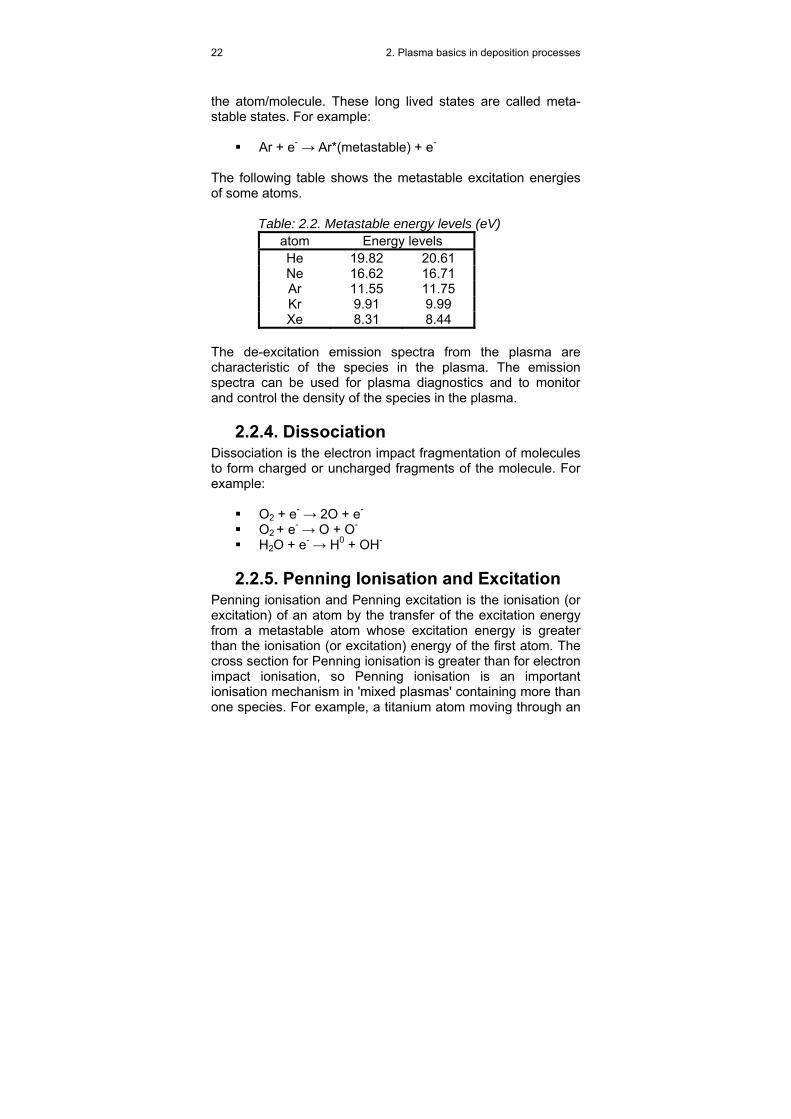
Ar + e- → Ar*(metastable) + e- The following table shows the metastable excitation energies of some atoms. Table: 2.2. Metastable energy levels (eV)
atom Energy levels He 19.82 20.61 Ne 16.62 16.71 Ar 11.55 11.75 Kr 9.91 9.99 Xe 8.31 8.44
The de-excitation emission spectra from the plasma are characteristic of the species in the plasma. The emission spectra can be used for plasma diagnostics and to monitor and control the density of the species in the plasma.
2.2.4. Dissociation Dissociation is the electron impact fragmentation of molecules to form charged or uncharged fragments of the molecule. For example:
O2 + e- → 2O + e- O2 + e- → O + O- H2O + e- → H0 + OH-
2.2.5. Penning Ionisation and Excitation Penning ionisation and Penning excitation is the ionisation (or excitation) of an atom by the transfer of the excitation energy from a metastable atom whose excitation energy is greater than the ionisation (or excitation) energy of the first atom. The cross section for Penning ionisation is greater than for electron impact ionisation, so Penning ionisation is an important ionisation mechanism in 'mixed plasmas' containing more than one species. For example, a titanium atom moving through an

2. Plasma basics in deposition processes 23
argon plasma can be ionised by collision with metastable argon atoms:
A* (metastable) + Ti → Ar + Ti+ +e- Ar has metastable states of 11,55eV and 11,75eV and the ionisation energy of Ti is 6,8eV. Thus a titanium atom colliding with a metastable argon atom is easily ionised. Metastable atoms may be very effective in ionizing other species by collision.
2.2.6. Charge Exchange Charge exchange occurs when an energetic ion passes close to a thermal neutral and there is a transfer of electron forming an energetic neutral and a thermal ion. This process gives rise to a spectrum of energies of the ions and neutrals in a plasma [13,14].
2.2.7. Plasma Activation Many of the plasma processes serve to plasma activate gases i.e. to make them more chemically active by dissociation, fragmentation, ionisation, excitation, forming new species, etc. These activated gases impinge on the substrate surface or, if ionised, can be accelerated to the substrate by a substrate bias thereby enhancing reactive deposition and reactive etching processes. Generally contaminant gases and vapours, such as water vapour and O2, in plasma-based processes are more significant than the same contaminant level in a simple vacuum-based deposition process because of the plasma activation.
2.2.8. Collision Processes A plasma can be viewed as a medium in which electrical or magnetic energies are transmitted into a gas. The energetic gas particles are then used to interact with the surface to produce desirable effects or to promote chemical reactions. Thus, the process of energy exchange during collisions involving plasma particles is of fundamental importance. Gas

24 2. Plasma basics in deposition processes
collision probabilities are often expressed in terms of a cross section σ which has the dimensions of an area. If an electron collided with a 'hard sphere' of radius a, then σ = π*a² (see Fig.2.2). The cross section is a measure of the probability that a given process will occur. For some complicated processes there may not be a corresponding physical picture as above, although σ still will have units of area. If we consider electron-neutral collisions where nn is the neutral density, then the quantity,
σ
λ⋅
=nn1
2-6
is the collision mean free path. This is the average distance travelled by the electron between collisions or processes.
a
Cross section
πa 2
'Hard Sphere' atom
e
e
-
-
Fig.2.2: Hard sphere atom cross section. Electrons that approach within a distance of the centre will undergo a collision, while those that have a larger impact parameter will not collide.
The total collision cross section can be written as othaionexeltotal σσσσσσ ++++= 2-7 where the subscripts el, ex, ion, a, and oth characterize the particular types of collision, namely elastic or momentum exchange, excitation, ionisation, attachment, and other processes, respectively.

2. Plasma basics in deposition processes 25
Another important quantity which is related to the cross section is the collision frequency ν. If ve is the electron velocity, the collision frequency ν is defined by ev⋅⋅= σν n 2-8 and has the unit s-1. The time between collisions is just ν-1. Collisions fall into two general categories: elastic collisions, which are those for which the internal energy of the colliding partners is unchanged by the collision, and inelastic collisions, in which internal energy changes. Internal energy refers to electronic excitations in atoms or electronic, vibrational and rotational excitations in molecules. Ions will, in general, have different states of internal energy, however, an electron does not. In weakly ionised plasmas (α<10-4), collisions between electrons and neutrals will be very important in establishing the electron energy distribution function. In fact, the dominance of electron-neutral collisions is responsible for the general character of these glow discharges, which behave very differently from plasmas with higher degrees of ionisation, where electron-electron collisions dominate.
2.2.9. Electron-Neutral elastic Collisions The elastic cross section for electron-neutral collisions σe-n will depend on the electron velocity [4]. For rare gases heavier than He, the cross section has a minimum at low electron velocities, rises to a peak which increases with mass, and falls off at higher velocities. The average amount of energy transferred from the electron to the neutral is εt, given by
EMm
t2
=ε 2-9
where E is the electron energy, m and M are the electron and neutral mass respectively. Since the neutral mass is much larger than the electron mass (2m/M = 1/40000), very little

26 2. Plasma basics in deposition processes
energy is transferred to the neutral species in an elastic collision. However, the electron will experience a large change in the direction of its velocity, and hence its momentum is changed.
2.2.10. Electron-Electron Collisions Electron-Electron collisions are characterised by a cross section σe-e which is given by
( )2220
4
v4lnm
eee
πεσ Λ⋅
=− where 2/1
2/3
212
nekT
⎟⎠⎞
⎜⎝⎛
=Λ
επ 2-10
m, e, v, n, T are the mass, charge, velocity, density and temperature of the electrons respectively. In electron-electron collisions, since the masses are equal, the electrons can exchange energy very effectively. Hence, electron-electron collisions will become important even at low degree of ionisation.
2.2.11. Electron impact ineleastic Collisions
Though the inelastic cross sections are often much smaller than the elastic ones, the electrons can lose a much larger fraction of its energy given by
EMm
M+
2-11
Since M>>m, virtually all of the electron energy is available for inelastic processes. Typical inelastic processes are: ionisation, electronic excitation, Penning processes, three body recombination, radiative recombination and dissociative processes. In rare gas atoms, electron excitation requires an amount of energy which is very close to that for ionisation, and therefore, the cross sections are quite similar. Owing to this,

2. Plasma basics in deposition processes 27
for rare gas plasmas, it can be assumed that where light is emitted (radiative decay following electron excitation), ionisation is probably also occurring. The excitation process represents an important energy loss mechanism for the electrons. Atoms, other than rare gases, will generally have lower lying levels for excitation, as will molecules, which have rotational and vibrational states which requires much less energy than excited electronic states. Electron energy losses will therefore be greater than in non-rare gas plasmas.
2.2.12. Reactions between heavy Species
Reactions between heavy species are those occurring during collisions of molecules, atoms, radicals and ions. These reactions can be grouped into two subcategories, namely, ion-molecule and radical-molecule reactions. Ion-molecule reactions are those that involve at least one ion. Radical-molecule reactions are the reactions occurring between neutral species only. The density of molecules in a gas at a pressure of about 1mbar is 4·1016 cm-3. In a plasma with a mean electron energy of 1eV, sustained in a gas characterised by a molecular dissociation energy of about 5eV and an ionisation energy of 10eV, the density of dissociated molecules can be estimated to be 1014 cm-3 [8]. The density of ions and electrons in a cold plasma is usually about 109 to 1011cm-3. Thus, in a cold plasma, the three densities are related by nri nnn <<<< 2-12 where nr is the radical density. Because of these relative particle densities, it can be expected that the radical-molecule reactions will be generally more important than will ion-molecule reactions in plasma chemistry. However, ion-molecule reactions can have significant contributions to plasma chemistry and can enhance the rate of the total reaction occurring in the plasma [9].

28 2. Plasma basics in deposition processes
There are a few ion impact processes which are crucial to the discharge. The first is secondary electron emission from a surface bombardment by an energetic ion. This process is usually characterised by a coefficient γ, which is the ratio of the number of electrons emitted for each incident ion. Typically 0,1 < γ*0,05. Another important ion process is that of charge transfer:
A+ + B → A + B+ where A and B can be the same species. This process is an important loss mechanism for energetic ions in the sheath region of discharges.
2.2.13. Ion Molecule Reactions Two colliding ions can recombine to form a molecule in the ground state and release their energy through emission of radiation:
A+ + B- → AB + hν This two-body recombination is important at very low pressures (<10-6mbar). A collision of two ions can also result in neutralization of the ions by forming of two excited atoms:
A+ + B- → A* + B* + hν Because the total energy of the recombining ions is generally larger then the total energy of the excited neutrals the surplus energy is released through radiation. Ion-ion recombination can also take place through a three-body collision:
M + A+ + B- → AB + M This three body recombination occurs at pressures above 10-6 mbar. An electric charge may be transferred during a collision between an ion and a neutral particle (charge transfer). The

2. Plasma basics in deposition processes 29
transfer can take place between identical partners, for example:
A + A+ → A+ + A Although this reaction has no effect, it results in fact in a slower ion and a faster neutral. These symmetric processes are characterised by large cross sections. At low energies, the asymmetric processes involving molecules (see below) are frequently characterised by large cross sections, whereas the ones involving atoms are characterised by small cross sections.
B2 + A+ → B2+ + A or A+ + BC → A + BC+
When the charge transfer takes place with dissociation of the colliding species, the reaction is called: charge transfer with dissociation:
A+BC → A + B+ +C The reaction rate constants of ion-molecule charge transfer reactions are typically of the order 10-10 to 10-12 cm³s-1 [57]. Transfer of heavy reactants is the type of ion molecule reactions that result in the formation of new compound species:
A+ + BC → (AB+ + C)/(AB + C+) The reactions are sometimes called ionisation by interchange. Examples of such transfer reactions are:
N+ + O2 → NO* + O
N + O2+ → NO+ +O
These reactions of heavy reactant transfer occur with rate coefficients greater than 10-9 cm³s-1.

30 2. Plasma basics in deposition processes
Radical-molecule reactions are those where only neutral species act as reactants. The active radicals may be either multi-atom radicals or single atoms or fragments of multi-atomic molecules. The radicals are unstable and chemically very active. Representative radical-molecule reactions are:
Electron transfer: A + B → A+ + B- This type of reaction requires that at least one molecule has very high kinetic energy and its occurance in cold plasmas is therefore rare.
Ionisation: A + B → A* + B + e- The Penning reactions occur during collisions involving energetic matastable species. In the collision of metastable (B*) with neutral species, the excited metastables transfer their excess energy to the target, causing ionisation or dissociation:
Penning ionisation:B* + A → A+ + B + e-
Penning dissociation:B* + A2 → 2A + B The penning processes are particularly important in plasmas sustained in mixtures, which include gases such as Ar and He, that are characterised by large cross section, which enhances the probability of this process. For penning reactions to take place, the energy of the metastable species must be higher than the ionisation or dissociation potential of the other species participating in the reaction. Metastable energies are in the range of 0-20eV. For example for nitrogen for certain gases at lower energies, the cross sections for metastable excitation are much higher than the cross sections for ionisation. In such conditions, electron impact causes formation of a larger number of metastable particles than ions.
2.2.14. Diffusion and Particle Losses At pressures typical for deposition and etching (10-4 mbar –10-1 mbar), the loss of charged particles by the volume processes

2. Plasma basics in deposition processes 31
discussed above are relatively small. The dominant charged particles loss-mechanism is diffusion and convection to the vacuum chamber boundaries, where recombination will occur rapidly on the solid surfaces.
SnDtn
=∇•∇+δδ
2-13
with n the particle density, D the diffusion coefficient, and S the net volume production rate. The choice for the diffusion coefficient is dependent on a number of things. At low enough densities, the diffusion coefficient is given by [10]
ν3
v2
=D 2-14
where v is the particle velocity and ν is the collision frequency for momentum transfer. This means that electrons would tend to diffuse much faster than ions. However, as the electron and ion densities become greater, electric fields will arise because of this disparity in diffusion rates, and this will tend to equalize the rates. This latter type of diffusion is called ambipolar, and in the extreme limit, which occurs for electron densities above 109cm-3, both electrons and ions diffuse at two times the slower ion rate [11, 12].

32 2. Plasma basics in deposition processes
2.3. Configurations for generating Plasmas
In generating and sustaining plasmas, energy is imparted to electrons by electric field and the energetic electrons create ionisation by electron-atom collisions. Electrons in a plasma originate from: secondary emission processes from ion or electron bombarded surfaces (secondary electrons), ionizing gasphase collisions and electrons from a thermo-electron emitting source (hot cathode).
2.3.1. DC Plasma Discharges A low-pressure cold cathode discharge is one which is maintained primarily by secondary electrons emitted from the cathode due to bombardment by ions from the plasma. These secondary electrons are accelerated in the cathode dark space and enter the negative glow, where they are known as primary electrons. Each primary electron must produce a sufficient number of ions to result in the ejection of another secondary electron from the cathode. Under equilibrium conditions, enough electrons are produced to create enough ions which create enough electrons to sustain the discharge. The cold cathode DC diode discharge operates in the abnormal glow discharge region, where the cathode current density depends on the applied voltage. Fig. 2.3 shows a DC diode discharge configuration and the potential drop across the inter-electrode space. The cathode fall region is where most of the potential drop in a DC discharge is to be found. If conditions, such as potential, gas species or gas pressure change, the equilibrium condition will change. The energetic ion bombardment of the cathode surface also results in physical sputtering. The ions being accelerated to the cathode will experience physical collisions in the gas phase and lose some of their energy. Some of the ions being accelerated to the cathode may become neutralized by charge-exchange processes and this produces a spectrum of high energy neutral species. The result is a spectrum of high energy ions and neutrals bombarding the cathode. The DC diode

2. Plasma basics in deposition processes 33
configuration requires that the cathode consists of an electrically conductive material since a dielectric cathodic surface will build up a positive surface charge that prevents further high energy bombardment. Most of the bombardment energy goes into the cathode heating, requiring active cooling of the cathode in most cases.
anodecathode
negative glow plasma
cathode dark space substare position
+
-primary electrons
+ - +-
-
+-AA
groundpotential
+
-
cathode fall region
DC potential distribution
Ion induced secondary emission
Fig.2.3: Direct current (DC) diode discharge In the DC diode discharge configuration the plasma-generation region is primarily near the cathode, however the plasma fills the entire volume. In a hot cathode DC diode discharge, hot thermo electron-emitting surfaces at a negative potential, emit electrons that provide the electrons to sustain the discharge. This configuration can also use the electrons to evaporate material for deposition [15, 16]. The hot cathode discharge can be operated at lower pressures than the cold cathode DC discharge since the electron flux does not depend on the ion

34 2. Plasma basics in deposition processes
flux. Very high plasma densities can be achieved in a hot cathode system. In triode configuration the plasma is established between a cathode and an anode and ions are extracted from the plasma by a third electrode using a DC or RF potential to give bombardment of a surface [17, 18]. Often the triode system uses a hot cathode and the electrons are confined by a weak magnetic field (5-50mT) directed along the anode-cathode axis. The DC diode discharge cannot be used to sputter dielectric target materials, since charge build up on the cathode surface will prevent bombardment of the surface. If there are reactive gases in the plasma their reaction with the target surface can lead to the formation of a surface that has a different chemical composition than the original one. This change in composition leads to poisoning of the cathode surface and thus changes the plasma parameters. In the extreme, poisoning will cause bombardment of the cathode to cease due to surface charge build-up. If an insulating surface forms on the DC cathode, charge build-up will cause arching over the surface. The suppression of arcs generated in the DC discharge (arc suppression) is important to obtaining stable performance of the DC power supplies particularly when reactively sputter depositing dielectric films. Arcing can occur anytime a hot (thermo-electron emitting) spot is formed or when surfaces charging is different over surfaces in contact with the plasma. Arc suppression is obtained by momentarily turning off the power supply or by applying a positive bias when an arc is detected [29].
2.3.2. Pulsed DC Plasma Pulsed DC uses generally a potential operating in the range 50-300 kHz where the voltage, pulse width, off time and pulse polarity can be varied [19]. The pulse can be unipolar, where the voltage is typically negative with a no-voltage off-time, or bipolar where the voltage polarity alternates between negative and positive perhaps with an off time. The bipolar pulse can be symmetric, where the positive and negative pulse heights are equal and the pulse duration can be varied or asymmetric with
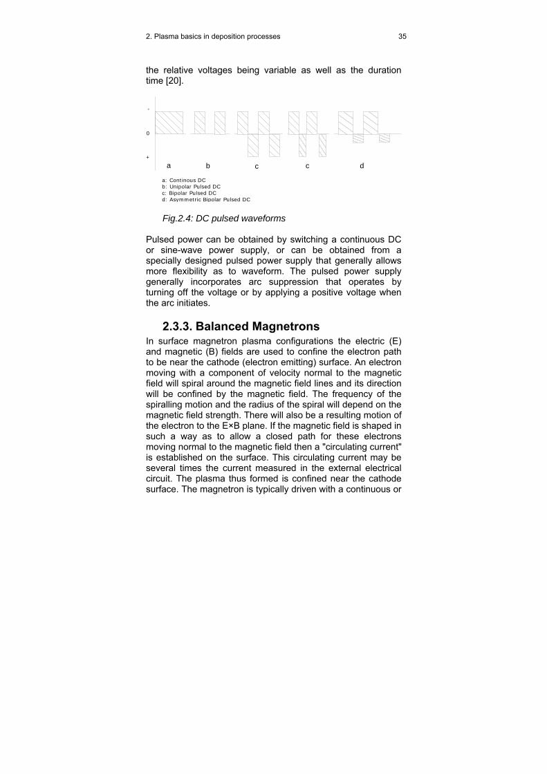
2. Plasma basics in deposition processes 35
the relative voltages being variable as well as the duration time [20].
0
+
-
a: Continous DCb: Unipolar Pulsed DCc: Bipolar Pulsed DCd: Asymmetric Bipolar Pulsed DC
a b c c d
Fig.2.4: DC pulsed waveforms Pulsed power can be obtained by switching a continuous DC or sine-wave power supply, or can be obtained from a specially designed pulsed power supply that generally allows more flexibility as to waveform. The pulsed power supply generally incorporates arc suppression that operates by turning off the voltage or by applying a positive voltage when the arc initiates.
2.3.3. Balanced Magnetrons In surface magnetron plasma configurations the electric (E) and magnetic (B) fields are used to confine the electron path to be near the cathode (electron emitting) surface. An electron moving with a component of velocity normal to the magnetic field will spiral around the magnetic field lines and its direction will be confined by the magnetic field. The frequency of the spiralling motion and the radius of the spiral will depend on the magnetic field strength. There will also be a resulting motion of the electron to the E×B plane. If the magnetic field is shaped in such a way as to allow a closed path for these electrons moving normal to the magnetic field then a "circulating current" is established on the surface. This circulating current may be several times the current measured in the external electrical circuit. The plasma thus formed is confined near the cathode surface. The magnetron is typically driven with a continuous or

36 2. Plasma basics in deposition processes
pulsed DC potential. Magnetic fields can be generated using permanent magnets or electromagnets. A major problem in using magnetic fields is the difficulty in obtaining a uniform field over a surface. This non-uniformity in the magnetic field produces a non-uniform plasma and this means non-uniform bombardment of the cathode surface and non-uniform sputtering of the cathode material. In order to increase the uniformity the plasma can be moved over the target surface by moving the magnetic field or the target surface may be moved in the magnetic field. An RF bias can be superimposed on the continuous DC potential in order to establish a plasma away from the cathode. This is useful in ion plating and reactive sputter deposition where the plasma is used to activate the reactive species and provide ions for concurrent ion bombardment of the growing film.
2.3.4. Unbalanced Magnetrons Unbalanced magnetron is the term given to magnetic configurations where some of the electrons are allowed to escape [21, 22, 23]. Most magnetrons have some degree of unbalance but in the application of unbalanced magnetrons, the magnetic fields are deliberately arranged to allow electrons to escape. These electrons then create a plasma away from the magnetron surface. Such a plasma can provide the ions for bombardment of the substrate during ion plating and/or can activate a reactive gas in reactive deposition processes. The magnetic field for unbalancing the magnetron configuration can be supplied either by permanent magnets or by electromagnets. Balanced and unbalanced magnetron configurations are shown in Fig. 2.5 and 2.6.

2. Plasma basics in deposition processes 37
Dense plasma
N NS
Balanced Magnetron
Sputtering target
Circulating electron path
N
N
SV-
Magnetic field linesB
Planar Magnetron
N NS
BB
Dense plasma
Magnetic field coils
Plasma
Unbalanced Magnetron
Sputtering target
Internal magnetsV-
Magnetic field lines
Cylindrical Post Magnetron
Fig.2.5: Balanced and unbalanced magnetron configurations
Fig.2.6: Schematic of the plasma confinement in balanced (left) and unbalanced (right) magnetron configurations
2.3.5. Radio Frequency (RF) Diode Discharge
In a capacitively-coupled radio frequency (RF) discharge, the electrons are forced to oscillate in the gas between the RF electrodes, thus gaining energy and by collision with atoms create ions, radicals and more electrons. RF power supplies operate at frequencies from kHz to the microwave band (GHz)

38 2. Plasma basics in deposition processes
with peak to peak voltages of greater than 1 kV and a power of up to 10Wcm-2 on the electrodes. The plasma acts as a low density electrical conductor and the RF field penetrates quite some distance into the plasma. In the RF diode system the plasma generation region is primarily between the electrodes. At high frequencies the massive ions only respond to the time-averaged electric field while the electrons move to and away from the electrodes creating high sheath potentials. The plasma will always be positive with respect to the large area electrodes and other surfaces. In addition to the bias imposed by the RF field, a DC bias can be imposed on the surface by placing a blocking capacitor in the RF circuit or by having a DC potential applied from a DC source through an RF choke id the area of the grounded walls in contact with the plasma is large, i.e., if the plasma potential is determined by grounded walls. Typically an RF discharge is established at 5*10-4 to 10-2mbar and has an electron density of 109 - 10¹¹cm-3 [24, 25]. Impedance matching networks are used to couple the maximum amount of power into the plasma by reducing the reflected power. In capacitively-coupled RF discharges, the plasma potential, and hence the sheath potential at the electrodes, can have a time-varying value of tens to hundreds of volts. When the electrodes have a different effective area, the plasma potential can also have a large DC potential with respect to one or more of the electrodes These factors affect the distribution of ion energies incident on the electrode surface in an RF discharge [26, 27, 28]. In plasma processing, the RF discharge has the advantage that insulating surfaces or insulating films on conductive surfaces can be bombarded by applying an RF potential. Disadvantages are: high power inputs (heating) to insulating materials cause cracking, electrode geometries can cause problems with coupling the RF power, RF power loss in systems, plasma uniformity is difficult to obtain and the bias conditions on surfaces in the RF plasma are variable and often difficult to control.

2. Plasma basics in deposition processes 39
2.3.6. Arc Plasmas Vacuum arc plasmas are formed by passing a low voltage-high current DC current (arc) between closely-spaced electrodes in a vacuum [31, 32]. This arc vaporizes electrode material, allowing a plasma to form in the vapour between the two electrodes [30]. In the arc there is appreciable ionisation of both the gas and the electrode material and many of the ions are multiply charged. It has been found that the ions from a vacuum arc have a high kinetic energy (50-75eV for single charged ions) due to a positive space charge formed above the cathode surface that accelerates the ions away from that region. In film deposition it is common to accelerate the gas ions and the film ions to the substrates using an applied negative potential on the substrates. Cathodic arc film deposition processes use a solid water cooled cathode as the source of the deposition material while the anodic arc deposition process uses a molten anode for the vapour source [33].
2.3.7. Laser induced Plasmas Lasers can be used to vaporize surfaces and the laser passing through the vapour cloud can ionise a high percentage of the vapour. Laser vaporization is sometimes called laser ablation. Typically an excimer laser (YAG or ArF) is used to deposit energy in pulses. The deposition energy can be greater than 5·1010 Wcm-2. The vaporized material forms a plume above the surface where some of the laser energy is adsorbed and ionisation and excitation occurs. In laser vaporization the ejected material is highly directed [34].
2.3.8. Microwave Discharges Plasmas can also be excited at quite high frequencies - 300 MHz to 1 GHz - where electron cyclotron resonance coupling gives more efficient ionisation [35]. Microwave discharges differ in many essential respects from DC and RF discharges: There is an increased amount of excitation in the discharge and a lot of vacuum-UV is produced, a high degree of ionisation (up to 20%), the electron densities are higher (109-

40 2. Plasma basics in deposition processes
1010cm-3) and the particle temperatures are higher. Microwave plasmas are most used in the downstream processing configuration since the substrates in the microwave cavity can detune the system.
2.3.9. Electron Emitter Discharge In the DC diode and RF plasma configurations, the electrons necessary to sustain the plasma are produced in the plasma. When using electron emitters, the electron source is independent of the plasma processes. Common electron emitters are hot thermo-electron emitting cathodic surfaces and hollow cathodes [36]. For example: hot LaB6 surfaces can give an electron emission of >20A/cm² at 1700°C. These discharges may have very high densities (10¹² cm-3). Often the electrons confined by a magnetic field directed along the anode-cathode axis. The magnetic field increases the electron path length in its movement from the cathode to the anode by causing the electron to spiral in the magnetic field. This increases the ionisation efficiency of the electron and allows the discharge to sustain at low gas pressures. The ions in the plasma may be extracted using an electrode at a DC or RF potential to give bombardment of a surface. In plasma processing some of the advantages of the electron emitter configurations are: the flux of electrons is independent of other plasma and electrode processes, very high plasma densities, the plasma properties can be controlled by controlling the electron emission and the electron beam can be used as a source for thermally vaporizing material. Disadvantages are: the need for well controlled and long life electron emitting sources and the plasma non-uniformity over large areas and complex surfaces.
2.3.10. Plasma Enhancement Plasma enhancement techniques may also be used to locally increase the plasma density. This plasma enhancement may be done by using rf fields [37], Thermo-electron emitting surfaces [38], hallow cathode electron emitters [39, 40], deflection of secondary electrons in e-beam evaporation, localized higher gas pressure, etc. The plasma density may

2. Plasma basics in deposition processes 41
also be increased by the use of magnetic fields which cause the electrons to spiral around the magnetic field lines thus increasing their path length (magnetron configurations). In some film deposition processes, ions of the film material (condensible or non-condensible) may be formed in plasmas by conventional techniques. High concentrations of ionised condensible film species may be formed:
in plasmas having high density of low energy (100eV) electrons
in vacuum arc plasmas on solid cathodes [41] above molten anodes in vacuum arc plasmas [42]
In many cases, these species may be multiply ionised. The addition of a reactive gas to the plasma allows the deposition of compound materials [43]. When using plasmas and bombardment effects in ion plating, many processing variables are often unknown:
the portion of the substrate current that is due to secondary electron emission
the flux and energy spectrum of the ions and electrons the flux, adsorption and surface coverage of the
neutral gaseous species.
Generally these plasma parameters are controlled by processing variables such as:
system geometry vaporization rate gas pressure gas composition gas flow rates substrate and system temperatures contaminants in the plasma substrate power input per unit area (voltage and
current). The plasma is a very energetic chemical environment and many chemical processes can occur. The principal chemical processes are [2]:
electron impact ionisation

42 2. Plasma basics in deposition processes
dissociation (fragmentation) of molecules (formation of radicals)
Penning ionisation (metastable collision) dissociative electron attachment electron attachment excitation momentum transfer collisions de-excitation of excited species recombination (neutralization)
Many of these processes are characterised by cross sections for collision processes and threshold energies for attachment processes. The degree of ionisation, dissociation and excitation of the species in a plasma depends strongly on the gaseous species, electron energy and density of the plasma. Generally there is much more dissociation than ionisation of molecular species. Many of these plasma processes serve to activate (plasma activation) the gas species, i.e. to make them more chemically active by dissociation, ionisation, or excitation. Plasma discharges are very effective in desorbing contaminates from surfaces in a plasma processing chamber. These impurities are activated in the plasma and may contaminate the depositing material. A number of techniques may be used to determine plasma properties [7, 54-56]. Optical emission and absorption techniques and quadrupol mass spectroscopy are the most common plasma analysing techniques. Electron and ion densities in a plasma may be measured by the use of small-area Langmuir probes and ion current densities are determined by so called Faraday-Cups.
2.3.11. Surface Reactions and Bombardment Effects
The physical effects of energetic particles bombardment on surfaces and depositing films is very dependent on the mass, flux and energy of the bombarding particles, the flux of non-energetic particles (i.e. depositing or absorbing species) and the atomic mass and chemical nature of the bombarded surface. Bombardment can be from ions accelerated to the

2. Plasma basics in deposition processes 43
surface under an impressed bias, an induced bias or due to the development of a sheath potential. Bombardment can also be from energetic neutrals formed by charge exchange processes or by the neutralization and reflection of energetic ions from a surface. The parameters (flux, energy, ratio) which are important for the film growth are usually poorly defined, and in many instances, the importance of bombarding is not recognized. Also many macroscopic film properties (i.e. refractive index, film stress, optical losses) can be correlated with the energetic particle bombardment of the growing film. Fig.2.5. shows several regions affected by particle bombardment [2].
reflected ions or neutrals
secondary electrons
sputtered atoms or ions
backsputtered
surface
surface
channelingcollision cascade
energetic particle
enhanced surfacemobility
adsorbed surfacespecies
displacementimplanted
lattice defectstrapping
enhanced chemicalreactions
redeposited
surf
ace
regio
nnea
r s u
r fac
e r e
gio
n
Fig.2.7: Schematic description of energetic particle bombardment effects on surfaces and growing films
Surface: Interface between solid and gas (vapour or
vacuum) Surface region: Region of physical penetration by the
bombarding particles in which there is a collision cascade
Near surface region: Region beyond physical penetration but which is affected by the bombardment (heating, diffusion)
Bulk region: Region of the material which is not significantly affected by the bombardment

44 2. Plasma basics in deposition processes
The effects of bombardment of energetic species (ions, neutrals) on the surface and the surface region include:
1. desorption of weakly bonded surface species 2. ejection of secondary electrons 3. reflection of the energetic species as high energetic
neutrals 4. sputter ejection of surface atoms by momentum
transfer through collision cascades 5. sputtering and re-deposition of sputtered species 6. enhanced mobility of surface atoms 7. enhanced chemical reaction of impinging and
adsorbed species. In the subsurface region
1. the impinging particles may be physically implanted 2. the collision cascades cause displacement of atoms
and the creation of lattice defects 3. surface species may be recoil-implanted into the
surface lattice 4. mobile species may be trapped at lattice defects 5. particle kinetic energy is mostly converted into heat
2.3.12. Collisional Effects The collisional effects due to the bombardment of energetic particles during film deposition can produce a large variety of effects in the growing film and can be classed as being either structural or chemical in nature. In reality, the net effect to the film is generally a combination of both types of phenomena. These effects can appear as structural modifications to the crystal structure and orientation of the film, changes to the average grain size of the film, modifications to the film stress, incorporation of inert gases within the film, modification of lattice constants and numerous other film property changes. Chemically, the film can be made purer, with better adhesion to the substrate, and the relative stoichiometry of the film can be altered over a broad range. These changes can subsequently affect such properties as the film density, film porosity, mechanical stress, adhesion, electrical resistance,

2. Plasma basics in deposition processes 45
refractive index, optical absorption, stability on air and surface topography. The main processes responsible for these changes in the film properties are momentum transfer (knock-on) displacement and direct temperature effects (thermal annealing due to temperature rise caused by thermal spikes). These processes can cause various effects as the thin film grows, including enhanced surface mobility, enhanced accretion of nuclei, desorption of surface impurities, redistribution of atoms in the film, and also the implantation of bombarding species into the growing film.

46 3. Ion and Plasma assisted PVD
3. Ion and Plasma assisted PVD Processes
The use of plasma and ion-assisted PVD deposition processes for the deposition of compounds (oxides, carbides, nitrides and sulfides, etc.) has spread into various types of industrial applications. These include dielectric films in microelectronic, optics and magnetic applications, hard carbide and nitride films for cutting and forming tools, sulphides for solid state lubrication and solid state electrolytes, etc. Energetic ions and/or activated species in the vapour phase are employed in these processes for surface treatment, deposition and etching. This presence of energetic particle influences the film growth mechanism and the resulting optical and mechanical properties of the films. All plasma processes for thin film deposition described in this chapter have been carefully investigated by the various plasma analytic methods described in chapter 4. Seven different processes have been investigated in respect to their energetic situation of the plasma and the resulting film properties: Reactive Low Voltage Ion Plating - RLVIP, Reactive Advanced Plasma Source Ion Plating - RAPSIP, Arc Source Deposition - ASD, Pulsed Laser Ablation Deposition – PLAD, Magnetron Sputtering DC continuous and DC pulsed – DC-MS, DC-PMS.
3.1. Ion Beam Assisted Deposition (IBAD)
A significant advance in the technique of reactive evaporation has been made by the introduction of directed ion beams. It was originally proposed by Auwärter [47] that the reactivity of the residual gas could be increased by ionisation and the first practical demonstration of the effectiveness of the idea was made by Heitmann [48, 49]. The investigations in this work were done on an IAD process with an End-Hall type ion gun in use [50, 51]. This ion source has been developed for high current, low energy ion beam applications. Beam currents up to 1A have been obtained at mean ion energies of 30-120eV using Ar, Kr or O2. The end-

3. Ion and Plasma assisted PVD 47
Hall source should be useful in applications where large currents of low energy ions are used in conjunction with thin film deposition to increase adhesion, modify stress, increase density or hardness, produce a preferred orientation or improve step coverage. The high current densities enable the substrate surfaces to be sputter cleaned prior to film deposition. The effect of surface charging in the case of insulating substrates can be minimized by an electron-emitting filament mounted in the ion beam or close to the substrate. The area of the substrate subjected to ion bombardment is dependent upon the ion gun aperture, beam divergence and source to substrate distance. Typical beam divergence is 10°. Typically operation pressure of the chamber is in the range of 10−4 mbar. The technique is highly directional and therefore limited to line of sight geometries, but leads to considerable control over properties of the growing films. A cross section of the investigated end-Hall ion source and a schematic diagram of this source is shown in Fig. 3.1.
Fig.3.1: left: Schematic of End-Hall Ion Source, right: Cross section of the shape of the magnetic field in the discharge region The electron emission from the cathode is controlled with the cathode supply. The anode potential is controlled by the anode current, the strength of the magnetic field and the gas

48 3. Ion and Plasma assisted PVD
flow. The shape of the magnetic field in the discharge region is indicated in Fig. 3.2. One major mechanism by which a potential difference is generated in a magnetic field (to accelerate the ions) is the reduced plasma conductivity across magnetic field lines.
Fig.3.2: Schematic diagram of the electrical power supply of the ion source Ions are generated in the discharge plasma and accelerated into the ion beam. The potential of the discharge plasma extends over a substantial range. As a result, the ions have an equivalent range of kinetic energy after being accelerated into the ion beam. The mean energies were obtained on the ion beam axis. Charge exchange and momentum exchange processes with the background gas in the vacuum chamber result in an excess of low-energy ions at large angles to the beam axis [51]. These processes are to be believed to be the cause of most of the observed variation in the mean energy with off-axis angle. Analysis of the discharge process indicated that neutralisation should be obtained when the cathode emission is approximately equal to the anode current, or slightly negative.

3. Ion and Plasma assisted PVD 49
The end-Hall source generates low-energy, high current beams of ions. The beam profiles are reproducible and well suited for broad-area coverage of a target. Because it is also simple, mechanically rugged and reliable, end-Hall sources are well suited for property enhancement applications in a production environment. In ion beam sputtering (IBS), shown schematically in Fig.3.3, the target erosion is produced by a mono-energetic argon ion beam usually from a broad beam ion source [76]. In dual ion beam sputtering a second ion gun is used with the beam directed at the growing film similar to ion beam assisted deposition. As with gas discharge sputtering IB-sputtering yields dense, well adherent and stoichiometric films with low optical absorption and stable properties. Concerning total optical losses in all-dielectric coatings ion beam sputtering seems to be the superior technology [74].
Fig.3.3: left: Schematic of ion beam sputtering, right: schematic of dual ion beam sputtering.
3.2. Ion Plating (IP) Ion plating is a generic term applied to atomistic film deposition processes in which the substrate surface and the growing film are subjected to a flux of energetic bombarding particles sufficient to cause changes in the film formation process and the properties of the deposited film. This broad definition does not specify the source of the depositing film particles, the source of bombarding particles, nor the environment in which the deposition takes place. The principle criterion is that energetic particle bombardment is used to modify the film formation process and film properties [45].

50 3. Ion and Plasma assisted PVD
In a conventional ion plating process [44] evaporation is performed in the presence of an argon gas discharge. Due to collisions and electron impact reactions, coating material ions are formed and accelerated in the electric field of biased substrates so that condensation and film formation take place under influence of ion bombardment.
a) b)
c)
Fig.3.3: Three different schematics of ion plating systems: a) Principle schematic from D.M. Mattox [44, 45] with a-Ar inlet, b-dark space shield, c-substrate, d-plasma at >10-1 Pa, e-evaporator, f-heating, g-flange to pumping system b) Ion plating system with conventional evaporator and additional ion source for generating a separate ion beam with a-recipient, b-substrate, c- evaporating particles, d-ion beam,

3. Ion and Plasma assisted PVD 51
e-ion source, f- gas inlet, g-voltage sources, h-flange to pumping system, i-evaporator c) Triode ion plating system with a-evaporator, b-substrate, d-vacuum flange to pumping system It can involve ions of the working gas, of the reactive gas, of the film material or of a mixture of the different components. In addition the higher energetic neutral atoms and molecules of the vapour and gas are also very important for the deposition process. This complex action is typically for ion plating. A large number of process variants is possible and different components can be combined to more complex triode and tetrode ion plating systems. It is furthermore remarkable that also high-speed sputtering cathodes are used as vapour sources in special ion plating arrangements. Bias sputtering and some types of plasma CVD also fall under the definition of ion plating.
Fig.3.4: Schematic of an industrial ion plating system (Oerlikon Balzers Coating Austria GmbH, www.balzers.at)
52 3. Ion and Plasma assisted PVD
The basic rules for ion plating are [2]: Bombardment must be over the whole surface to be
covered - the more uniform the bombardment (species, number and energy) the better
A minimum bombardment ratio and particle energy must be established in order to attain the desired property and structural modification of the surface and deposited film
Bombardment must be continued through the film formation stage in order to modify film composition, morphology, microstructure and properties
Contamination in the plasma should be low in order to reduce reaction with the substrate and with the depositing material (reactive species are activated in the plasma - good for reactive deposition, bad for contamination)
More material must be deposited than is removed by the bombardment process; however, all of the deposited material may react with the substrate giving a type of substrate modification coating.
In conventional ion plating the degree of ionisation is low and so the acceleration voltage must be rather high, generally between 3 and 5keV, to supply the necessary energy for the formation of well adherent and dense films. The small number of ions is also disadvantageous for a reactive gas process. Therefore, to overcome these problems, a special form of reactive ion plating process was developed at Balzers laboratory [46].
3.3. Reactive Low Voltage Ion Plating (RLVIP)
The reactive low voltage ion plating process (RLVIP) is performed in a specially designed automatic box type plating system Balzers BAP800, which is shown in Fig.3.5-3.7. This process can be used for the deposition of single layer and multilayer oxide and nitrate coatings onto unheated glass and other substrates [71-74].

3. Ion and Plasma assisted PVD 53
All evaporations are made by two special 270°-type evaporators. The starting materials, metal or sub-oxides, form electrically conducting melts. Very effective ionisation and activation of the evaporation coating material atoms and the admitted reactive gas components occur by a low-voltage high-current argon plasma beam (hot cathode type) directed to the crucibles (anode). The substrate holder is electrically insulated. In contact with the formed plasma cloud the substrates receive a relatively high negative self-biasing potential of 15V to 20V with respect to the plasma, which acts as an accelerating voltage for the positive ions. This potential, together with the repulsive force of the anode, determines the kinetic energy of the positive ions bombarding and forming the growing film. The total pressure in the plant is in the low 10−3mbar range. The film deposition is started and stopped by opening or closing moveable shutters in front of the e-gun.
Fig.3.5: Schematic of the RLVIP system

54 3. Ion and Plasma assisted PVD
Film thickness and deposition rate are controlled by a quartz crystal monitor (Fig.3.5). Standard parameter set used in the RLVIP process:
Deposition rate: 0,5 nm/s arc-current: 15A - 60A (variation)
0,05mA/cm2 - 0,33mA/cm2 arc-voltage: 55V (constant) anode-voltage: 35V (constant)
Fig.3.6: Ion Plating system BAP800 from Balzers at University of Innsbruck, Institute of Ion Physics

3. Ion and Plasma assisted PVD 55
Fig.3.7: Modern industrial Ion Plating system BAP800 from Balzers Optical thickness monitoring can be used too. Quarterwave films in the visible are deposited within four to five minutes. Uniformity in thickness distribution of ±1% over the whole substrate holder of 800 mm diameter can be achieved by the use of a static correction shield. The BAP 800 can be tooled for both reactive ion plating and conventional reactive evaporation allowing alternating processes without requiring any changes in the plant.
Fig.3.8: RLVIP TiN process plasma (working gas: Ar, reactive gas: N2)

56 3. Ion and Plasma assisted PVD
3.4. Reactive Advanced Plasma Source Ion Plating (RAPSIP)
Another ion plating technology is based on the use of the advanced plasma source APS from LEYBOLD. The high power plasma source is a relatively new development [76-78] which is applied in a batch box-coater system. The principle of the RAPSIP is shown in Fig.3.9 [74]. Plasma Ion Assisted Deposition is considerably improving the properties of evaporated or sputtered thin films by high energy ion bombardment during the growing of the film. The RAPSIP process allows the production of dense shift free thin films with high refractive index, good adhesion and extremely low absorption. Due to the low process temperature RAPSIP is suitable especially for heat-sensitive substrates. The APS provides high ion current densities over a large surface area in a neutral plasma to produce high quality layers at a high productivity. The electron beam guns all have a 270° beam deflection. The various crucible inserts enable a range of coating materials to be employed. The electron beam can be moved in an x and y direction for optimal erosion of the material. The plasma source, which consists of a large area LaB6-cathode, a cylindrical anode tube and a solenoid magnet is placed in the centre of the plating chamber bottom next to the electron beam evaporators. The large cylindrical LaB6-cathode is heated indirectly by a graphite filament heater.

3. Ion and Plasma assisted PVD 57
Fig.3.9: Principle schematic of the RAPSIP process with the APS from Leybold A DC glow discharge plasma in Ar is switched on. The solenoid magnet surrounding the source forces axial directions of the electrons. Due to the magnetic field the electrons move into direction of the substrate holder. They spiral along the magnetic field lines thus extracting the plasma into the coating chamber. The reactive gas inlet in form of a ring shower is located on the top of the anode tube. Blown directly into the dense plasma the reactive gas is ionised and activated. Since the dense plasma fills the total volume of the chamber, the evaporant also becomes partly ionised. The generation of the plasma is completely separated from evaporation, therefore the process is compatible with any evaporation material like metals, semiconductors, sub-oxides and oxides.

58 3. Ion and Plasma assisted PVD
Fig.3.10: APS plasma source With the APS 8 kW plasma power are possible and a total ion current of 5 A with excellent uniformity over a large substrate holder surface of about 1m2 can be achieved [65]. It is further possible to use the APS for a plasma enhanced chemical vapour deposition PECVD process. There is an additional gas inlet for a monomer gas to be added to the plasma leading to a deposition process of e.g. a hydrophobic top-coat on the surface of an anti-reflectance coating of ophthalmic lenses [66].
Fig.3.11: APS 1100 vacuum plant The great potential of the plasma plating process with LEYBOLD’s APS source has been demonstrated by the fact

3. Ion and Plasma assisted PVD 59
that the film properties of dielectrics as well as of metals are fundamentally improved in comparison to conventional evaporation even without additional substrate heating. This happens mainly because of the ion plating effect in the coating process. Therefore the plasma plating-technology is also useful for high quality coatings on organic substrates. Special coating systems (SYRUS) and coating processes such as Duraplas and Safire have been developed for successfully coating plastic lenses in ophthalmics [75].
3.5. Arc Source Deposition (ASD) Arc vapour deposition is a PVD technique which uses the vaporization from an electrode under arcing conditions as a source of vaporised materials. Arcing conditions consist of a high-current (≅ 50-500A), low-voltage (≅ 20V) electric arc passing through a gas or a vapour of the electrode material and running on a conducting target [64]. Once triggered it sustains itself in vacuum by producing an almost fully ionised and directed plasma beam of the target material. The plasma is generated at small discrete sites at the cathode surface known as cathode spots. The spot size has been estimated as 1-100μm and its current density as 104-108A/cm2 [62, 63].
Fig.3.12: Principle of arc source evaporation The plasma pressure within the cathode spot is high, and a strong pressure gradient causes the plasma generated there

60 3. Ion and Plasma assisted PVD
to expand. The plasma plumes away from the cathode, initially normal to the cathode surface and in the general direction to the anode. This quasi neutral plasma plume is the medium that conducts the arc current and enables the arc to persist. The vacuum arc plasma contains electrons, ions, atoms and macro-particles. The ions can provide useful bombardment of a growing film either at their neutral energy or at another energy determined by the level of direct-current (DC) or radio frequency (RF) bias applied to the substrate. The neutral ion energy is high (tens of eV) compared with other plasma deposition techniques.
Fig.3.13: Evolution and development of an arc spot Ion bombardment at the cathode and electron bombardment at the anode heat the electrodes. Most of the ejected material is thermally evaporated but some is ejected as molten droplets or solid particles from the cathode. A high percentage of the vaporised atoms are ionised in the arc process. The arc can be established between closely spaced electrodes in a good

3. Ion and Plasma assisted PVD 61
vacuum (vacuum arc) by vaporising some of the electrode material, or between electrodes in a low-pressure or high-pressure gaseous environment (gaseous arc). In PVD processing, arc vaporisation can be considered a unique vaporisation source along with thermal vaporisation and sputtering [30, 31, 32, 61, 62, 67].
Fig.3.14: Schematic of an industrial Arc Source Deposition system (Oerlikon Balzers Coating Austria GmbH, www.balzers.at) If the vaporisation primarily occurs from the cathode surface by arc erosion the system is called a continuous cathodic arc source. The cathode can be molten or solid with a water cooled solid cathode (cold cathode). The cold cathode source is the most common cathodic arc source for thin film deposition.

62 3. Ion and Plasma assisted PVD
Fig.3.15: Images of the arc running on target surface In order for a stable arc to form there must be a minimum current passing through the arc (app. between 50A to 10A for low melting materials like Cu and Ti and 300A to 400A for refractory materials such as tungsten). The arc voltage can be from 15V to 100V depending on the ease of electron motion from the cathode to the anode (cathode design). Problems with the cathodic arc technique include stabilisation and movement of the arc on the solid surface and the formation of molten micron-sized (0,1-10μm) particles (macros) of the ejected material from the solid cathode surface. If the arc is allowed to move randomly over the surface the arc source is called a random arc source. If the arc is confined and caused to move over the surface in a particular path the source is called a steered arc source. Steered arc sources generally produce fewer macros than random sources. Macro particles, ejected due to heating of the cathode surface, are the main disadvantage of the vacuum arc technique. If incorporated in a growing film they cause defects and surface roughness. To overcome this problem different filtered arc systems are in use there the macro particles and the neutral atoms are filtered by guiding it through a region of curved magnetic field, so that the line of sight from the cathode to the substrate is obstructed.

3. Ion and Plasma assisted PVD 63
Fig.3.16: Industrial Arc Source Deposition plant (Oerlikon Balzers Coating Austria GmbH, www.balzers.at)
3.6. Pulsed Laser Ablation Deposition (PLAD)
The pulsed laser ablation deposition (PLAD) method is based on physical processes, arising from the impact of high power pulsed laser radiation on solid targets and leading to the removal of partially ionised material (plasma) from the impact zone [69, 70]. The properties of the deposited films depend strongly on the deposition characteristics and can be controlled by changing the process parameters. Usually a background gas is added to control the kinetic energy of the plasma species or to increase the content of light elements, e.g. oxygen, in the film.

64 3. Ion and Plasma assisted PVD
Fig.3.19: Principle set up of PLA: The experimental set-up is simple, but the ablation process itself is extremely complex involving the interaction between the laser and a solid target material, plasma formation and the transport of material across the vacuum to the substrate. (taken from http://www.pvd-coatings.co.uk) Formation of the plasma flux characteristics in PLAD starts with laser radiation interaction with the target. At pulsed laser flux densities of 105-1010 Wcm-2, as used in PLAD, the quasi stationary target evaporation regime is reached, where the temperature of the evaporating surface T0 remains constant. A plasma is formed on the target spot and a large amount of material ions are ejected from the plasma plume. A specific feature of the PLAD fluxes is their high degree of ionisation and high kinetic ion energy, which depend on experimental conditions, such as laser radiation flux density, wave length, target material, and the temporal shape of the laser pulse [70]. Typical pulse duration is between 20 and 200ns with repetition rates between 20 and 150Hz. At nanosecond pulse duration for example the energy spectrum of the ions is in the region of 0eV to 2000eV with a mean energy of 100eV to 400eV. The ionisation degree of the plasma is between 10% and 70% and depends strongly on the energetic and spectral laser parameters. The neutral component of the plasma flux has

3. Ion and Plasma assisted PVD 65
relatively low mean energy (∼10eV) [70] and comprises 30% to 90% of the evaporated material, depending on the thermophysical properties of the target and on the laser parameters. CO2-lasers, Nd-YAG lasers and excimer lasers are generally used for PLAD techniques. Growth of films by PLAD is a process that depends on many factors, such as density, energy, ionisation degree, type of condensing particles, as well as the temperature and physiochemical properties of the substrate [68, 69]. Thermal and kinetic energy of the plasma particles can significantly influence some film properties.
3.7. DC Magnetron Sputtering (DC-MS)
The development of high performance magnetron sputtering sources that provide relatively high deposition rates, large deposition areas, and low substrate heating, revolutionised the sputtering process by greatly expanding the range of feasible applications. Magnetron sputtering sources can be defined as diode devices in which magnetic fields are used in contact with the cathode surface to form electron traps which are so configured that the BxE
velectron drift currents close upon
themselves. Magnetron can be configured in a variety of forms. Examples would be planar magnetrons, S-gun type or cylindrical types [52, 53]. Depositions done at low argon working gas pressures (10−3 and 10−4 mbar) and target-substrate distances of 5 to 15cm show that, the higher energy of the sputtered atoms result in good film quality, even then the substrates are unheated. Besides metal-sputtering also reactive processes e.g. for oxide or nitride formation are possible. The invention of magnetron cathodes improved the sputter rate. High frequency sputtering can be applied for depositing insulating chemical compounds from insulating targets, but low deposition rates and target cooling problems restrict often the use of this technique in practice. These limitations have been overcome by the introduction of magnetron sputtering and, unbalanced magnetron sputtering, dual magnetron sputtering and different magnetron configurations with additional dc or

66 3. Ion and Plasma assisted PVD
pulsed bias supply [91]. State of the art in gas-discharge sputtering is the use of twin or dual magnetron sputter cathodes, operated in dc or pulsed dc mode [89, 90].
3.8. DC Magnetron Sputtering with DC Biasing (DC-BMS)
A standard planar dc magnetron source was supplied in this configuration with an additional dc bias on a steel grid mounted on the inner part of the cylindric recipient, and was isolated from the magnetron source and from the substrate plane, which was on ground potential. A Ti target was used under Ar/N2 atmosphere depositing TiN coatings. The sputter plasma has been investigated by varying the bias voltage from dc to 80V at a total gas pressure in the mid 10−3 mbar range (pAr=3,2*10−3mbar - 23sccm and pN2=0,8*10−3mbar - 5,5sccm).
Fig.3.20: Schematic of a magnetron sputtering process with additional dc biasing
3.9. DC Pulsed Magnetron Sputtering (DC-PMS)
Nowadays, pulsed ion-plasma processing is finding increasingly broader application in the production of various

3. Ion and Plasma assisted PVD 67
devices and tools for microelectronics, engineering, medicine, etc. The methods of pulsed ion-plasma technology allow one to reduce the temperature of a treated sample, to increase the adhesion and density of deposited films, to improve the quality of coatings on dielectric surfaces, and to deposit multilayer coatings. Various constructions of ion-plasma system for pulsed processing of materials are described in the scientific literature, as well as the technological processes of deposition for different coatings based on these systems. Pulsing the bias voltage has been found to significantly increase the ion current drawn at the substrate [92]. Usually in magnetron systems, the fluxes of ions are controlled by the substrate bias voltage and it has been found that the current drawn at the substrate saturates at bias voltages of the order of -100V [93]. Further increases in the bias voltage do not lead to a further increase in current, which seems not to be the case in the pulsed bias configurations, where not only the magnitude of the saturation current is grater than for the dc bias case, but also the current drawn at the substrate also continues to increase as the bias voltage is increased and in addition both of these effects become more marked as the pulse frequency is increased.
a)

68 3. Ion and Plasma assisted PVD
PPM 421 Smart Probe
Magnetron target
Race track
Sputtercoater Edwards 500
62 mm
500mm
b) Fig.3.22: a) Schematic of a reactive dc pulsed magnetron sputtering plant; b) Schematic of the plasma measurements in the dc pulsed magnetron sputtering process, showing the position of the plasma monitoring system PPM421 (Inficon) and the Langmuir probe system (Scientific Instruments) Pulsed sputtering has been introduced to stabilize reactive magnetron deposition processes. During recent years several investigations have indicated that pulsed powering not only remarkably improves the process stability, but also increases energetic particle bombardment of the substrate and the growing film. Pulsed dc uses a potential in the range of 10 to 350 kHz where the voltage, pulse width, off time and pulse polarity can be varied. The pulse can be unipolar, where the voltage is typically negative with a zero voltage off-time, or bipolar where the voltage polarity alternates between negative and positive. Pulsed power can be obtained by switching a continuous dc or sinewave power supply, or can be obtained from a specially designed pulsed power supply that generally allows more flexibility as to waveform.

4. Diagnostic methods 69
4. Diagnostic methods
4.1. Langmuir Probes Langmuir probes are one of the oldest and probably the simplest plasma diagnostic methods. The technique consists of inserting small metallic electrodes (wires) or probes of known area into the plasma. The usual shapes of these probes are spheres, cylinders and planes. The probe is connected electrically to a variable voltage power supply, which in turn is connected to a second reference electrode immersed in the plasma. The reference electrode is, in the case of single probes, very much larger than the probe itself and could typically be the anode or cathode of an electrically generated plasma, the metallic walls of the chamber containing the plasma or any other convenient conducting surface in contact with the plasma. So called double Langmuir probes have reference electrodes with similar size and shape as the probe.
U
I
anode
cathode
single probe
I
U
cathode
anodedouble probe
plasma plasma
Fig.4.1: Principal setup of Langmuir probes The principle setup of a single and a double Langmuir probe and a typical current-voltage (I-U) characteristic of a single probe is shown in Fig. 4.1 and 4.2. As simple as the technical setup is for the probe, a major difficult with Langmuir probe techniques is the fact that in general very complex

70 4. Diagnostic methods
computational schemes are necessary to obtain the plasma parameters from the measured I-U characteristic.
VpVf
U
I
0
A B Celectron saturationion saturation
electron retardation Fig.4.2: I-U characteristic of Langmuir probe Furthermore, for r.f. or magnetically supported discharges there are additional factors which may introduce further complications. Plasma parameters which can be extracted from Langmuir probe measurements are:
Plasma Floating Potential - Vf Plasma Potential - Vp Electron temperature - kTe Electron number density - ne Ion number density – ni Electron energy distribution function - EEDF Debye length - λD
The qualitative behaviour of the I-U curve can be explained in the following way. The potential Vp is called the plasma potential and is the potential that exists between the plasma and the reference electrode (earth potential of vacuum chamber in the case of using single probes).

4. Diagnostic methods 71
Fig.4.3: Principal system configuration of Langmuir system SmartProbe from Scientific Instruments When the probe is at this potential there is no electric field between the probe and the plasma and the current collected is entirely due to the random motion of the charged particles. The ratio of the electron current to the positive ion current is approximately given by:
2/1
⎟⎟⎠
⎞⎜⎜⎝
⎛≅
ei
ie
i
e
MTMT
II
4-1
where Te is the electron temperature, Ti the ion temperature and Me and Mi the respective masses of electrons and ions. For example in an Ar plasma, even if Te=Ti the ratio Mi/Me is 270, and therefore when the probe is at the plasma potential the current can be assumed to be entirely an electron current. When the probe is biased positively with respect to the

72 4. Diagnostic methods
plasma, the positive ions are repelled and the electrons are attracted. There is a negative charge build up near the probe surface which cancels the positive charge on the probe. This is the situation described by the region C of the I-U curve in Fig. 4.2., which is called electron saturation. If the probe bias is decreased below the plasma potential, positive ions are attracted to the probe, the ion concentration near the probe gradually increases and the formation of a positive ion sheath around the probe is observed. With decreasing bias, the ionic component of the current increases and the portion B of the I-U characteristic, known as transition region or electron retardation is obtained. At Vf, which is called the floating potential, the electron and ion current is exactly equal and so the net current drawn by the probe is zero. This is the potential which will be assumed by an insulator inserted into the plasma. By further decreasing the bias of the probe, the current becomes completely ionic and the region A of the characteristic, which is called ion saturation region, is obtained. In general only region A and B of the characteristic are used to determine the plasma parameters since the large currents drawn in region C greatly disturb the plasma under investigation. The extension of this disturbing region, which is confined to the sheath region, is approximately equal to the Debye length λD of the plasma. For a plasma of undisturbed density n and for which Te >>Ti the Debye length is given:
2/1
24⎟⎠⎞
⎜⎝⎛=
nekTe
D πλ 4-2
where k is the Boltzmann constant and e the electronic charge. One of the fundamental characteristics of a plasma is that they shield themselves from any externally imposed disturbance within a distance of the order of their Debye length. The analytical description of the I-U characteristic of an electrostatic probe is in general a very complicated task and depends not only on the plasma investigated but also on the geometry of the probe used. In general, the Debye length of

4. Diagnostic methods 73
the plasmas used in deposition technologies is 10-2 to 10-3 cm. Futhermore, since the pressures in these processes are below 10-1 mbar, the mean free path for collisions between charged and neutral particles is of the order of cm. Under these circumstances, it can be assumed that charged particles collected by the probe do not undergo any collisions in the sheath region collision less sheath. Basically there are three operation regimes which are classified according to their ratio of the probe radius rp to the Debye length λD [55-57].
rp/λD>>10: In this limit, the sheath, surrounding the probe is very thin and does not change appreciable with the voltage. Simple analytical expressions can be found for the probe current. However, it is practically impossible to operate in this regime since the large probe dimensions required will greatly distort the plasma.
rp ≅ λD: In this regime, the expressions describing the collected current become a set of non-linear integral equations which can only be solved numerically.
rp/λD<<1: This is the OML (orbital motion limited) regime in which the analytical expressions for the probe current are quite simple and the requirements on the probe dimensions are not so critical.
Theory of Ion Collection in a Collision Less Plasma About two decades ago Laframboise developed a general technique for numerically solving the equations for the probe current and hence predicting the ion current collected by a spherical or cylindrical probe [58]. Laframboise’s results are very accurate, in good agreement with experiment, and very general. They cover essentially the whole range of probe-plasma conditions of practical interest and are easy to use. Laframboise assumes that both the electrons and the ions have Maxwellian velocity distributions far from the probe and he investigates in detail the two situations in which the ions either cold or at the same temperature as the electrons. He does however provide sufficient information for the

74 4. Diagnostic methods
experimentalist to interpolate with confidence for any value of ion to electron temperature within this range. For a cylindrical probe of length l, the collected ion current is given as
ii
epi i
mkT
lrneI2/1
2 ⎟⎟
⎠
⎞⎜⎜⎝
⎛=
π 4-3
where mi is the ion mass and ii is a dimensionless ion current which can be seen in Fig. 4.3. For an experimental measured value of Ii and a calculated electron temperature Te from the retarding field part of the I-U characteristic, the ionisation density can be deduced from Eq.4.3 and Fig.4.4. Because ii is itself a weak function of the density, an iterative procedure is required, but convergence is rapid [54].
0 5 10 15 20 250
1
2
3
4
5
6
100
10
5
4
0
ion
curr
ent:
i i
probe potential: -V
Fig.4.4: Ion current versus probe potential for various ratios of rp=λD for an ion attracting cylindrical probe with Ti=Te =0,1 [58]
Determination of the Floating Potential There are a number of direct methods for measuring the plasma potential. The knee of a single probe characteristic can

4. Diagnostic methods 75
in principal be directly used. However, large electron currents are drawn, this is often very unreliable. The easiest and most convenient potential to identify on a probe characteristic is the floating potential Vf (potential for which the net current to the probe is zero). Hence the experimentalist measures the potential from this point and corrects these values with the calculated value of Vf. As its definition indicates Vf can be calculated by equating the electron current to the ion current. In a Maxwellian plasma and for a cylindrical probe operating in the OML regime the electron and ion current is given by
⎟⎟⎠
⎞⎜⎜⎝
⎛⎟⎟⎠
⎞⎜⎜⎝
⎛=
ee kT
eVAeNI expm2
kT
2/1
e
e
π 4-4
2/1
i
i2/1 1
m 2kT
2⎟⎟⎠
⎞⎜⎜⎝
⎛−⎟⎟
⎠
⎞⎜⎜⎝
⎛=
ii kT
eVAeNIππ
4-5
where A is the probe area and Ii and Ie represent the ionic and electronic current respectively. Setting Ii=Ie for V=Vf and taking into account that Ti << Te it follows
⎟⎟⎠
⎞⎜⎜⎝
⎛=⎟⎟
⎠
⎞⎜⎜⎝
⎛−⎟⎟
⎠
⎞⎜⎜⎝
⎛
e
f
e
f
i
e
kTeV
kTeV
mm
exp22/12/1
2/1π 4-6
This equation gives for an argon plasma: Vf = - 4;7*Te (Te in eV and Vf in volts) The actual distribution for electrons can be obtained directly by determining the second derivative of the probe current which can be shown to be proportional to the velocity distribution [59]. The presence of a magnetic field does not appreciably influence the motion of the positive ions. Therefore, in the case of magnetically supported discharges Eq.4-5 still gives the ionic current. However, the electronic current is no longer given by Eq.4-4 but this equation can still be used to determine the correct electron temperature, since it appears that the voltage dependence is still of the form exp(eV/kTe). However, the relationship between the floating potential and

76 4. Diagnostic methods
the electron temperature can only be obtained if the form of the pre-exponential term in the expression for the electronic current is known for the magnetically supported discharges.
Analysis Techniques The Langmuir probe measurements were carried out with an automated Langmuir probe plasma diagnostic system from Scientific Systems. The principal setup of this system is shown in Fig.4.3 and 4.5.
Fig.4.5: Schematic of Langmuir measurement in a RLVIP process Data acquisition, system control and the data analysis and calculations were done by a special software program called SmartSoft [60]. There are two analysis routines available in SmartSoft that operate on the measured I-U characteristic and calculate the plasma potential Vp, the floating potential Vf , the electron temperature kTe, the electron number density ne and

4. Diagnostic methods 77
the Debye length λD. The two analysis routines are Zero Second Derivative and Intersecting Slopes.
Fig.4.6: SmartSoft print out, showing the I-U diagram and the calculated plasma properties Zero Second Derivation The zero second derivation is the simpler of the two analysis routines. The plasma potential Vp is defined as the voltage at which the second derivative is equal to zero
02
2
=dV
Id
The I-U characteristics goes through an inflection at the plasma potential. The negative potential which develops on the floating probe is known as the floating potential. There is no net current flow through the probe and Vf will repel sufficient electrons to equate the ion and the electron fluxes. On the I-U curve Vf is the voltage at which the current is equal

78 4. Diagnostic methods
to zero. The electron temperature is calculated by taking the current measured at the plasma potential I(Vp) and dividing it by the integral of the I-U curve from Vf to Vp, i.e.:
e
p
kTdVI
VI 1)(
)(=
∫ υ 4-7
This method of calculating kTe is not sensitive to noise unlike the more common technique of calculating kTe by dividing I(Vp) by the derivative of the I-U characteristic. The electron number density ne is calculated from the current measured at the plasma potential using the following equation:
2/1
2
2)(⎟⎟⎠
⎞⎜⎜⎝
⎛=
e
e
p
pe kTe
mAVI
nπ
4-8
Ap is the area of the probe, me the mass of the electron, e is the electronic charge and kTe is the electron temperature in eV. The negative sheath which develops around the probe has a defined length known as the Debye length λD which is calculated from the electron temperature using the following equation:
2/1
20
⎟⎟⎠
⎞⎜⎜⎝
⎛=
e
eD ne
kTελ 4-9
Intersecting Slopes The “intersecting slopes” analysis routine is an alternative technique of estimating Vp from the I-U curve. The current measured above the plasma potential is extrapolated back to a point where it intersects with the slope of the exponential part of the I-U curve. The intersection point gives the plasma potential. The electron number density and electron temperature are then calculated using the same equations as in the zero second derivative routines.

4. Diagnostic methods 79
4.2. Faraday Cups Faraday Cups are used mainly in thin .lm technology to measure the ion current density. This could be helpful to get information about the ion current distribution of a plasma or ion source or the distribution in the substrate plane. A schematic of a special Faraday Cup, which can be used for investigating the ion current density on different places in the substrate plane is shown in Fig.4.7.
Ie
U2=0...40V
U1=-30Vgrids
metallicelectrode
signalion current
B
+++
++
+
++
--
--
-
-
-
magnetic field -deflecting electrons
Plasma
redarding voltage - energy select+
+
++
reflection of secondary emission electrons
Fig.4.7: Schematic setup of a Faraday Cup A magnetic field at the entrance of the Faraday Cup deflects the electrons, so that there is only a positive ion current into the Faraday Cup. Inside the Cup the ions have to overcome the positive variable potential U2 (0-30V) (retarding potential), therefore only ions with a higher energy than this retarding potential U2 are able to reach the electrode, there they impact and an electron is drawn from the power supply. This

80 4. Diagnostic methods
representative electron current can be measured by an ampere meter. Calculating the first derivation of the ion current density:
2dUdji
leads to the ion frequency at a certain energy level. The impact of higher energy ions on the metallic electrode can result in the emission of secondary electrons, which compensate an ion charge and falsify the measurement. The third grid, which is on a potential of U1=-30V, reflects the secondary emission electrons back to the metallic electrode. With the ampere meter an electron current is measured, which is necessary for the recombination of the incoming ions. In a typical measurement run, the retarding voltage U2 is increased from 0V until the measured ion current is zero. The decrease of the ion current with increasing potential U2 is proportional to the number of ions with an energy of U2*q. Then the decrease of the ion current in a certain step U2+ΔU is high, the number of ions with an appropriate energy is also high and so the first derivation of the ion current density dji/dU is a representative for the ion frequency at a certain energy level. A typical result of a measurement is shown in Fig.4.8.
0 5 10 15 20 250
10
20
30
40
50
60
ion current density
ion frequency
ion
curr
ent d
ensi
ty [μA/cm
2 ]
redarding voltage [V]
0 5 10 15 20 25
0
1
2
3
4
ion
frequ
ency
Fig.4.8: Typical Faraday Cup measurement

4. Diagnostic methods 81
MIEDA (Multichannel Ion Energy Distribution Analyser) System The MIEDA system was developed at University of Innsbruck to measure automatically the ion current as a function of the kinetic energy of the ions due to a variation of the grid voltage (retarding potential – URPD) within the MIEDA sensor. The system consists of a data acquisition module, a variable voltage supply (0-500V), a fixed voltage supply, a controlling PC with the MIEDA Control Software and several special designed Faraday Cups - MIEDA sensors - to collect the ion currents at different positions.
Fig.4.9: MIEDA system overview
Fig.4.10: MIEDA sensors consisting of three grids with distance-rings between, a contacting print and a steel case The collected data show the value of the ion current at an certain ion energy and the first derivation of the ion current (di/dURPD) leads to the amount of ions in a certain energy

82 4. Diagnostic methods
interval. The system can be controlled by a graphical software application and the data are stored in an ASCII file.
Fig.4.11: Graphic user interface for control and data-acquisition
Fig.4.12: Assembly of the MIEDA-sensors: changeable grid-stack (left), sensor consisting of stack-base with cabling, grid-stack and enclosure (right)

4. Diagnostic methods 83
Fig.4.13: Changeable inner parts (grid sensors) of the Faraday Cup system MIEDA Following features are offered by the system:
Simultaneous and automatically measure of the ion current in dependence on different process parameters
Connection of several MIEDA sensors to measure simultaneous at different spatial positions in the vacuum chamber
Small and compact sensor construction and so less disturbance of the investigating plasma
MIEDA sensors can be built in instead of the substrate to investigate the plasma in a typical deposition process at the substrate position
MIEDA sensors can be built in the deposition shade to get a continuous control of the plasma during normal production processes
Storage and comparisation of plasma properties at different process parameters

84 4. Diagnostic methods
Fig.4.14: Several MIEDA sensors placed on different substrate positions to analyse the plasma in dependence on different process parameters in an APS (advanced plasma source) process
4.3. Plasma monitoring Quadrupol Mass Spectrometer with Energy Analysis
The used plasma monitoring system PPM421 (Inficon) consists of a quadrupol mass analyser QMA421 coupled with an energy filter as shown in Fig.4.15. The analysis system has to be operated at a pressure lower than 10-5mbar. Since most plasma processes, however, are operated in pressure ranges between 10-4mbar and a few mbar, the analysis tube has to be differentially pumped. The pressure difference is maintained by sampling the plasma through a 100μm hole in the extraction hood producing a pressure reduction of approximately 10-4, so that in the coating chamber a gas pressure during plasma analysis up to 1*10-¹mbar is possible.
400
300
200
100

4. Diagnostic methods 85
Fig.4.15: PPM421 setup - Plasma monitoring system from Inficon For ion sampling with minimum plasma disturbance the extraction hood is mounted in the substrate plane. The potential of the extraction hood can be floatable or can be set to a desired potential by an external voltage supply. The function of the elements between the extraction hood and the energy filter depends on the operating mode of the PPM421.

86 4. Diagnostic methods
Fig.4.16: PPM421 monitoring system set up in BAP800 vacuum chamber In the ion detection mode the ions entering from the plasma filled coating chamber through the entrance aperture are focused on the entrance of the energy filter by an optical system composed of the ENTRY lens, the ITRO lens and the FOC1 electrode. For the detection of neutrals the ITRO element serves as an ionisation chamber with an electron impact ion source. Ions are extracted from the ion source with the EXTR electrode and focused on the entrance of the energy filter by the FOC1 lens. The ionisation chamber can be operated on a potential of 0V to 150V. For plasma potentials lower than 150V this ensures an efficient suppression of ions produced in the plasma. The electron energy can be varied in the range between 8eV and 120eV. A cylindrically, electrostatic mirror analyser CMA is used for energy filtering. The mass filter is a standard quadrupol mass filter with Mo rods of 8mm in diameter and 200mm in length. It has a high transmission and an excellently low mass discrimination.

4. Diagnostic methods 87
Fig.4.17: Functional setup of the plasma monitoring system PPM 421 (Inficon, Liechtenstein) The energy and mass filtered positive or negative ions are detected with a 90° off axis secondary electron multiplier. It can be operated either in ion counting mode (with linear dynamic range from less than 0,1cps to 106cps), or in analog mode (for currents up to 10μA) as a preamplifier for an electrometer. The system offers a mass range of 1 to 512 amu and an energy range of -500eV to +500eV. The minimum energy resolution is 0,3eV. The whole system is software controlled (Quadstar 422) requiring no manual tuning. For the investigation of directional plasma effects, the whole system can be fixed to the coating chamber by a special tilting device. The device makes it possible to tilt the plasma monitor +/- 6° in each direction. So it is possible to direct the monitor in direction to the melts to investigate the ions and neutrals directly coming from deposition source.
4.4. OES Optical Emission Spectroscopy
The optical emission spectroscopy (OES) takes advantage of the light emitting properties of plasmas, to specify due to the measured spectral lines the ions and neutrals of the plasma. In such an arrangement the emitting light is collected by an

88 4. Diagnostic methods
optical fiber and lead to a grid monochromator. The light is spectral separated at the grid due to inflection, and only a certain wavelength can be seen at the output slit of the monochromator, which is directed to a photomultiplier to produce a current proportional to the intensity of the light. The emission spectra of the plasma then can be detected by mechanical twisting the grid by a stepping motor. To identify the light emitting particles in the plasma an accuracy for the monochromator of 0,1nm to 1nm is sufficient. However, significant lines of the spectra are not only in the visible range but also in the UV range, especially for pvd processes. The spectral range for an OES arrangement (fiber optic, grid, SEM) should be at least 200 to 800nm.
substrate
plasma source
Plasma
fiber optic
gridmonochromator
photo-multiplier
SEM
data aquisition
Vacuum chamber
PC +printer
Fig.4.18: OES principle setup The light which is emitted by the particles in the plasma in the VIS and UV range comes from the transition from electronic activated states into lower states. The most intensive transition is normally from the first activated state to the ground state of the particle. Each atom, molecule and ion has its specific, particle characterising, energy states E and radiates at the transition E1-E0 with a characteristic frequency of ν10=(E1-E0)/h which can be identified. The interpretation of the main lines are usually simple, however, the interpretation of the lines with less intensity or the identification of particles with low density is due to the richness of lines very difficult. It is also impossible to specify unknown species or complex molecules where the emission lines are not well known.

5. Experimental results 89
5. Experimental Measurements In the following chapters the results of the plasma analysis of different investigated ion and plasma assisted pvd processes will be presented. The plasma properties like the kind of ions, degree of ionisation, ion energy distribution, total ion current, ion and electron densities, as well as plasma and self-biasing potentials were analysed by means of
the mass spectrometric based plasma monitoring system PPM421 (kind of ion, degree of ionisation, ion energy distribution),
the Langmuir probe system (ion currents, densities and potentials)
the specially developed Farady-Cup MIEDA system (total ion current, ion energy distribution).
The principle setup and functionality of these different plasma analysing systems were already shown in Chapter 4. Selected pvd processes were carefully investigated. The properties of chemical compound films, deposited in reactive mode in the individual, plasma analysed pvd processes wre determined. Finally it was tried to correlate the plasma obtained characteristics with the measured film properties. Table: 5.1.1. Overview of investigated process technologies and deposited coatings
process technology coating material
RLVIP Ta2O5, TiN RAPSIP SiO2, Ta2O5, TiO2 DC-MS TiN DC-PMS Ta2O5, TiN PLAD TiC ASD TiN, CrN
RLVIP … Reactive Low Voltage Ion Plating RAPSIP … Reactive Advanced Plasma Source Ion Plating DC-MS … DC- Magnetron Sputtering DC-PMS … DC-Pulsed Magnetron Sputtering PLAD … Pulsed Laser Ablation Deposition ASD … Arc Source Deposition

90 5. Experimental results
5.1. RLVIP – Reactive Low Voltage Ion Plating
Fig.5.1.1: Experimental setup of the plasma measurements in the RLVIP process Typical process parameters:
Deposition rate: 0,5nm/s Total gas pressure: 1,0*10-3 – 2*10-2mbar,
typ.1,5*10-3mbar Ar pressure: 0,8*10-3mbar O2 or N2 pressure: 0,2*10-3 – 1,8*10-3mbar Arc current: 15A-80A, typ. 50A Ion current density: 0,05mA/cm2 – 0,45 mA/cm2 Arc voltage: app. 55V Anode voltage: app. 35V
1 … Substrate holder 2 … Plasma monitoring systems:
PPM421 or Langmuir Probe 3 … Shielding 4 … 270° e-gun 5 … Filament of plasma device 6 … Plasma source 7 … Inlet working gas: Ar 8 … Inlet reactive gas: O2 or N2 9 …Evaporation shutter 10 … Magnetic focusing of low
voltage, high current e-beam

5. Experimental results 91
5.1.1. RLVIP Ta2O5 film deposition In the RLVIP process the energy distribution of the gas molecules and film forming particles is strongly related to the arc current of the plasma device and is in the range from 5 to 35 eV, depending on the process parameters. In contact with the formed plasma cloud, the substrates receive a negative self-biasing potential of 5-15V with respect to the plasma depending on the process parameters. At a total gas pressure of 1.5*10-³mbar and an arc current of 50A the plasma potential in the substrate plane for example is 12V. This potential, together with the repulsive force of the anode (20-30V), determines the kinetic energy of the positive ions bombarding and forming stoichiometric compound films. The Ta2O5 coatings prepared by RLVIP are fully dense with a smooth surface even at low temperatures and show compressive stress. Typical process reactions:
2 Ta + 2,5 O2 → Ta2O5 2 TaO + 1,5 O2 → Ta2O5
The following plasma investigation were done in dependence on the two main process parameters in the RLVIP process, the arc current and the gas pressure. The most interessting film properties for Ta2O5 like refractive index, absorption coefficient and film stress will also be shown.

92 5. Experimental results
a) Plasma and film properties in dependence on the arc current: Plasma properties: The arc current, which is driven from the hot filament of the plasma source to the evaporation source, is the main parameter in the RLVIP process and is linearly correlated with the ion current density in the substrate plane (Fig. 5.1.2). The ion and electron density, in the range from 5*109 to 2*1010cm-3 (Fig. 5.1.9), also shows a quite linear dependence on the arc current. The kinetic energy of the plasma particles (material and gas atoms and molecules) are in the range from several eV up to 50eV (Fig.5.1.3), strongly dependent on the arc current (Fig. 5.1.4, 5.1.6, 5.1.7, 5.1.8). The energy distribution of the material particles like Ta+ and TaO+ (Fig. 5.1.4 and 5.1.8) is increased with increasing arc current and reaches a maximum with arc currents at 50A and higher in the range from 15eV to 45eV. The energy distribution of the gas particles like O+ and O2+ (Fig. 5.1.6, Fig. 5.1.7) changes from a low energy regime (0-20eV) to a distribution with a high energy peak at 20eV.
20 30 40 50 60 70 800,0
0,1
0,2
0,3
0,4
0,5
RLVIP Ta2O5 process under Ar/O2 atmosphere
file:curr_density_arcfrom J. Edlinger, Thesis 1990, University of Innsbruck
Ion current density in dependance on arc-current
curre
nt d
ensi
ty [m
A/c
m2 ]
arc-current [A]
Fig.5.1.2: Ion current density in dependence on the arc current

5. Experimental results 93
0 5 10 15 20 25 30 35 40 45 50 55102
103
104
105
106
TaO2+
Ta+
TaO++
TaO+Ta++
Ar+
O+
O+, O2++
Ar+
Ta++
TaO++
Ta+
TaO+
TaO2+
RLVIP process parameters: Ar/O2 atmosphereStarting material:Ta2O5
Starting pressure=2*10-5mbar
ptot=1,5*10-3mbar
pAr=1,0*10-3mbar
pO2=0,5*10-3mbar
Iarc=50AUarc=70V, Uanode=32V
file: e_1_i.opj
coun
ts
energy in eV
Fig.5.1.3: Energy distribution of the different ions in a Ta2O5 RLVIP process under Ar/O2 atmosphere
0 5 10 15 20 25 30 35 40 45 50 55102
103
104
105
106
80A
60A40A
20A Iarc=20A Iarc=40A Iarc=60A Iarc=80A
RLVIP process parametersRLVIP Ta2O5 process under Ar/O2 atmosphereStarting material:Ta2O5
ptot=1,5*10-3mbar
pAr=1,0*10-3mbar
pO2=0,5*10-3mbar
file: e_ta_i.opj
coun
ts
energy in eV
Fig.5.1.4: Energy distribution of the Ta+ ions in a Ta2O5 RLVIP process in dependence on the arc current under Ar/O2 atmosphere

94 5. Experimental results
20 30 40 50 60 70 80
10
15
20
25
file: e_max_ta
RLVIP process parametersStarting material: Ta2O5
ptot=1,5*10-3mbar
pAr=1,0*10-3mbar
pO2=0,5*10-3mbar
Iarc: variied
E max
in e
V
arc current in A
Fig.5.1.5: Maximum of energy distribution of the Ta+ ions in dependence on the arc current
0 5 10 15 20 25 30 35 40 45 50 55102
103
104
105
106
Iarc=20A Iarc=40A Iarc=60A Iarc=80A
RLVIP process parametersStarting material:Ta2O5
ptot=1,5*10-3mbar
pAr=1,0*10-3mbar
pO2
=0,5*10-3mbar
file: e_o2_i.opj
coun
ts
energy in eV
20A
40A
60A
80A
Fig.5.1.6: Energy distribution of the O2+ ions in a Ta2O5 RLVIP process in dependence on the arc current under Ar/O2 atmosphere
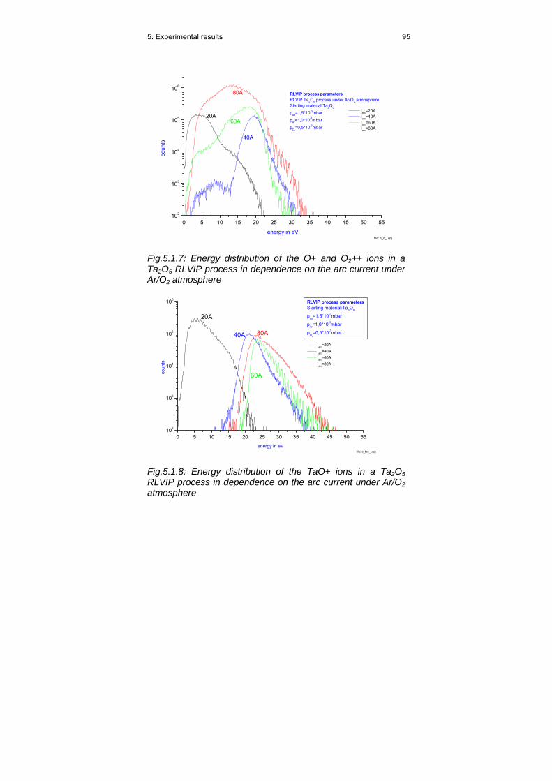
5. Experimental results 95
0 5 10 15 20 25 30 35 40 45 50 55102
103
104
105
106
80A
60A
40A
20A Iarc=20A Iarc=40A Iarc=60A Iarc=80A
RLVIP process parametersRLVIP Ta2O5 process under Ar/O2 atmosphereStarting material:Ta2O5
ptot=1,5*10-3mbar
pAr=1,0*10-3mbar
pO2=0,5*10-3mbar
file: e_o_i.opj
coun
ts
energy in eV
Fig.5.1.7: Energy distribution of the O+ and O2++ ions in a Ta2O5 RLVIP process in dependence on the arc current under Ar/O2 atmosphere
0 5 10 15 20 25 30 35 40 45 50 55102
103
104
105
106
Iarc=20A Iarc=40A Iarc=60A Iarc=80A
RLVIP process parametersStarting material:Ta2O5
ptot=1,5*10-3mbar
pAr=1,0*10-3mbar
pO2
=0,5*10-3mbar
file: e_tao_i.opj
coun
ts
energy in eV
20A
40A
60A
80A
Fig.5.1.8: Energy distribution of the TaO+ ions in a Ta2O5 RLVIP process in dependence on the arc current under Ar/O2 atmosphere

96 5. Experimental results
Fig.5.1.9: Density of charged particles – positive ions and electrons - in dependence on the arc current Film properties: An increase in the arc-current increases the refractive index of the deposited films due to rising film density caused by higher energetic film forming particles. Post deposition heat treatment causes relaxation of the high density films and decreases the refractive index. Where as a low density film, obtained with low arc-currents, is densified by the heat treatment and its refractive index is increased (Fig.5.1.10). The extinction coefficient, and so the optical losses, is increased with increasing arc currents (Fig. 5.1.11). Due to the higher kinetic energies of the bombarding particles more chemical defects are produced with higher arc currents. Higher arc currents increase film density and with it compressive film stress of RLVIP-Ta2O5 films reaching a maximum at about 60A and with still higher arc currents dimishing due to the onset of thermal induced film density relaxation. Extrapolations below 20A arc current yield low density films with tensile film stress (Fig.5.1.12).

5. Experimental results 97
Fig.5.1.10: Refractive index of Ta2O5 RLVIP thin films at 550nm in dependence on the arc current
Fig.5.1.11: Extinction coefficient (optical loss) in dependence on the arc current

98 5. Experimental results
Fig.5.1.12: Compressive film stress of Ta2O5 RLVIP thin films with 100nm thickness
b) Dependence of plasma and film properties on the gas pressure Plasma properties: In the following measurements the total gas pressure was increased from 1,5*10-3mbar to 3,0*10-3mbar by increasing the reactive gas component O2. The arc current was kept constant at 50A. The energy distribution of the gas particles like Ar+, O+ and O2+ is shifted to a lower energy regime with increasing total gas pressure due to a reduction in the mean free path of the ions and thus more collisions in the gas phase (Fig. 5.1.13-Fig. 5.1.15). This behaviour of a reduction of the kinetic energy with increasing total gas pressure also can be seen for the material particles like Ta+ and TaO+ (Fig.5.1.16 and Fig. 5.1.17).

5. Experimental results 99
0 5 10 15 20 25 30 35 40 45 50 55102
103
104
105
106
pO2=0,5*10-3mbar
pO2=1,0*10-3mbar
pO2=2,0*10-3mbar
RLVIP process parametersStarting material:Ta2O5
Iarc=50A
pAr=1,0*10-3mbar ptot, pO2
=variied
file: e_ar_i.opj
coun
ts
energy in eV
Fig.5.1.13: Ion energy distribution of Ar+ ions in a Ta2O5 RLVIP process in dependence on the gas pressure
0 5 10 15 20 25 30 35 40 45 50 55102
103
104
105
106
pO2=0,5*10-3mbar
pO2=1,0*10-3mbar
pO2=2,0*10-3mbar
RLVIP process parametersStarting material:Ta2O5
Iarc=50A
pAr=1,0*10-3mbar ptot, pO2
=variied
file: e_o2_i.opj
coun
ts
energy in eV
Fig.5.1.14: Ion energy distribution of O2+ ions in a Ta2O5 RLVIP process in dependence on the gas pressure

100 5. Experimental results
0 5 10 15 20 25 30 35 40 45 50 55102
103
104
105
106
pO2=0,5*10-3mbar
pO2=1,0*10-3mbar
pO2=2,0*10-3mbar
RLVIP process parametersStarting material:Ta2O5
Iarc=50A
pAr=1,0*10-3mbar ptot, pO2
=variied
file: e_o_i.opj
coun
ts
energy in eV
Fig.5.1.15: Ion energy distribution of O+ and O2++ ions in a Ta2O5 RLVIP process in dependence on the gas pressure
0 5 10 15 20 25 30 35 40 45 50 55102
103
104
105
106
pO2=0,5*10-3mbar
pO2=1,0*10-3mbar
pO2=2,0*10-3mbar
RLVIP process parametersStarting material:Ta
2O
5
Iarc=50A
pAr=1,0*10-3mbar ptot, pO2
=variied
file: e_ta_i.opj
coun
ts
energy in eV
Fig.5.1.16: Ion energy distribution of Ta+ ions in a Ta2O5 RLVIP process in dependence on the gas pressure

5. Experimental results 101
0 5 10 15 20 25 30 35 40 45 50 55102
103
104
105
106
pO2=0,5*10-3mbar
pO2=1,0*10-3mbar
pO2=2,0*10-3mbar
RLVIP process parametersStarting material:Ta2O5
Iarc=50A
pAr=1,0*10-3mbar ptot, pO2
=variied
file: e_tao_i.opj
coun
ts
energy in eV
Fig.5.1.17: Ion energy distribution of TaO+ ions in a Ta2O5 RLVIP process in dependence on the gas pressure Film properties: RLVIP Ta2O5 films evaporated from oxidic starting material showed a decrease of the refractive index with higher gas pressures obtained by stepwise addition of oxygen gas to a constant base pressure of argon pAr=0,4*10-3mbar. Post-deposition heat treatment resulted in a further decrease of the index (Fig.5.1.18). This behaviour is mainly caused by a decrease in density due to structural relaxation and post-deposition oxidation may also contribute to the observed effect. The effect is stronger for films with a higher index value. But even at a total gas pressure of 4,2*10-3mbar the films remained dense enough to prevent water vapour sorption. RLVIP-Ta2O5 films obtained under a high oxygen pressure yield very low absorbing stoichiometric films, when the deposition rate is carefully adapted to the automatic oxygen gas supply system by lowering deposition rate at the beginning of the deposition (Fig.5.1.19). It becomes obvious, that beginning with an oxygen gas pressure of pO2=2,5*10-3
mbar fully oxidized films are obtained. Lower oxygen pressure
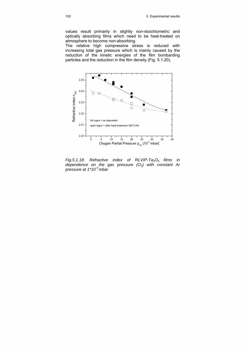
102 5. Experimental results
values result primarily in slightly non-stoichiometric and optically absorbing films which need to be heat-treated on atmosphere to become non-absorbing. The relative high compressive stress is reduced with increasing total gas pressure which is mainly caused by the reduction of the kinetic energies of the film bombarding particles and the reduction in the film density (Fig. 5.1.20).
0 5 10 15 20 25 30 35 402.20
2.21
2.22
2.23
2.24
2.25
open signs = after heat treatment 350°C/4h
full signs = as depositedRef
ract
ive
inde
x n 55
0
Oxygen Partial Pressure pO2 [10-4 mbar]
Fig.5.1.18: Refractive index of RLVIP-Ta2O5 films in dependence on the gas pressure (O2) with constant Ar pressure at 1*10-3 mbar

5. Experimental results 103
0 5 10 15 20 25 30 35 400
20
40
60
80
100
120
140
160
180
200
open signs = after heat treatment 350°C/4h
full signs = as deposited
Abs
orpt
ion
Coe
ffici
ent k
515 [
10-5]
Oxygen Partial Pressure pO2
[10-4 mbar]
Fig.5.1.19: Optical absorption of RLVIP-Ta2O5 films in dependence on the gas pressure (O2) with constant Ar pressure at 1*10-3 mbar
Fig.5.1.20: Compressive stress of RLVIP-Ta2O5 films in dependence on the gas pressure (O2) with constant Ar pressure at 1*10-3 mbar
8 10 12 14 16 18 20 22 24 26 28 30 32 34 36 38 40
-0,1
0,0
0,1
0,2
0,3
0,4
0,5
0,6
Com
pres
sive
Stre
ss σ
(G P
a)
Oxygen Partial Pressure pO2 (10-4 mbar)

104 5. Experimental results
Table 5.1.2: Summary of the results in the Ta2O5 RLVIP process:
Results Action Plasma properties Film properties
Increasing arc current
More electron impact
ionisation Higher plasma density Higher ion energy More energy input in the
films by bombarding particles
Increase of:
Refractive index Film density Optical absorption Intrinsic compressive
film stress
Increasing total gas pressure (O2 pressure)
Shorter mean free path Decrease of kinetic energy
of particles Decrease of energy input
into the growing film
Decrease of:
Film density Intrinsic compressive
film stress Decrease of optical
losses
The variation of the arc current and the total gas pressure shows that a higher energy input into the growing film and an increase of the high energetic ions due to a higher arc current, cause higher film density, a higher refractive index and higher intrinsic compressive stress in the deposited films.
5.1.2. RLVIP TiN film deposition In the RLVIP TiN process the dependence of the plasma properties on the arc current, in the range from 20A to 80A, was investigated. In a first step the energy distribution of the involved particles was measured by plasma monitoring (PPM421) and in a second series of experiments the electrical properties (ion current density and floating potential) and the plasma densities (ion density and electron density) were measured by a Langmuir Probe system. The energy distribution of the material (Ti+, TiN+) and gas particles (Ar+, N2+) are in the range from 10eV to 30eV depending on the arc current (Fig. 5.1.21 – Fig. 5.1.25).
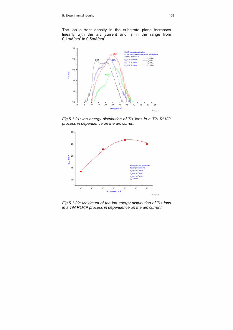
5. Experimental results 105
The ion current density in the substrate plane increases linearly with the arc current and is in the range from 0,1mA/cm2 to 0,5mA/cm2.
0 5 10 15 20 25 30 35 40 45 50 55102
103
104
105
106
107
60A
40A
80A
20A Iarc=20A Iarc=40A Iarc=60A Iarc=80A
RLVIP process parametersRLVIP TiN process under Ar/N2 atmosphereStarting material:Ti
ptot=1,5*10-3mbar
pAr=1,0*10-3mbar
pN2=0,5*10-3mbar
file: e_ti_i.opj
coun
ts
energy in eV
Fig.5.1.21: Ion energy distribution of Ti+ ions in a TiN RLVIP process in dependence on the arc current
20 30 40 50 60 70 80
10
15
20
25
30
file: e_max_ti
RLVIP process parametersStarting material: Ti
ptot=1,5*10-3mbar
pAr=1,0*10-3mbar
pN2=0,5*10-3mbar
Iarc: variied
E max
in e
V
Arc current in A
Fig.5.1.22: Maximum of the ion energy distribution of Ti+ ions in a TiN RLVIP process in dependence on the arc current

106 5. Experimental results
Fig.5.1.23: Ion energy distribution of Ar+ ions in a TiN RLVIP process in dependence on the arc current
0 5 10 15 20 25 30 35 40 45 50 55102
103
104
105
106
80A
60A
40A20A
Iarc=20A Iarc=40A Iarc=60A Iarc=80A
RLVIP process parameters: Ar/N2 atmosphereStarting material:Ti
ptot=1,5*10-3mbar
pAr=1,0*10-3mbar
pN2=0,5*10-3mbar
file: e_N2_i.opj
coun
ts
energy in eV
Fig.5.1.24: Ion energy distribution of N2+ ions in a TiN RLVIP process in dependence on the arc current
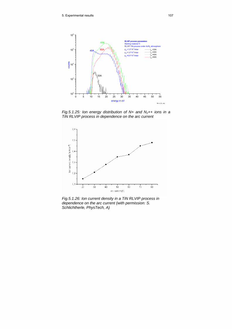
5. Experimental results 107
0 5 10 15 20 25 30 35 40 45 50 55102
103
104
105
106
80A
60A
40A
20A
Iarc=20A Iarc=40A Iarc=60A Iarc=80A
RLVIP process parametersStarting material:TiRLVIP TiN process under Ar/N2 atmosphere
ptot=1,5*10-3mbar
pAr=1,0*10-3mbar
pN2=0,5*10-3mbar
file: e_N_i.opj
coun
ts
energy in eV
Fig.5.1.25: Ion energy distribution of N+ and N2++ ions in a TiN RLVIP process in dependence on the arc current
Fig.5.1.26: Ion current density in a TiN RLVIP process in dependence on the arc current (with permission: S. Schlichtherle, PhysTech, A)

108 5. Experimental results
Measurements of the electrical potentials with Langmuir measurements (with permission: Stefan Schlichtherle, PhysTech Coating Technology, Pflach, A):
Fig.5.1.27: Setup and position of Langmuir probe measurements The following figures show the results of the Langmuir Probe measurements in the RLVIP process at three different positions in the substrate plane. The electron density (Fig. 5.1.28) and the ion density (Fig. 5.1.29) show a linear increase with increasing arc current from 20A to 80A in the range from 2*109cm-3 to 9*109cm-3. The floating potential is in the range 0,8V to 2V.

5. Experimental results 109
Fig.5.1.28: Electron density in the RLVIP process in dependence on the arc current
Fig.5.1.29: Ion density in the RLVIP process in dependence on the arc current
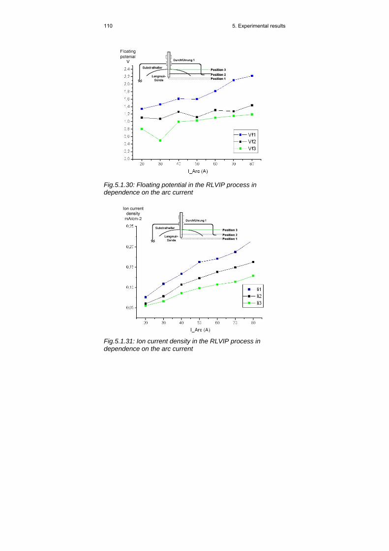
110 5. Experimental results
Fig.5.1.30: Floating potential in the RLVIP process in dependence on the arc current
Fig.5.1.31: Ion current density in the RLVIP process in dependence on the arc current

5. Experimental results 111
Table 5.1.3: Plasma potential in the RLVIP process:
5.1.3. Summary of the RLVIP process The results confirm that in the RLVIP process chemical compound formation is favoured by the activated (potential energy) and ionised (kinetic energy) states of the reaction partners during .lm formation. The film densities are high and the films are under compressive intrinsic stress when the depositions were performed at low total gas pressures (<pges=2.0*10-3mbar) and with arc-currents higher than 40A [91]. In the ion plating experiments an increase of the refractive index and the compressive film stress by densification of the bombarding particles due to larger arc currents and ion current density is observed. For both materials SiO2 and Ta2O5 it could be confirmed that the achieved refractive index and the compressive stress in RLVIP films is a consequence of film densification. A peening model for ion supported physical vapour deposition (PVD) film production predicts a saturation for the film densification and with it for the refractive index and the mechanical stress with increasing ion current densities (see also Chapter 5.7.3 and Ref. [110]). This prediction could also be confirmed by the measurements [91] demonstrated in Fig.5.1.10 and 5.1.12. It can be assumed that a constant Ar pressure in the RLVIP process means also a constant number of Ar+ ions, formed mainly by electron impact in the ion source, the place of the Ar inlet. An increasing number of O2 molecules, admitted directly into the coating chamber close to the e-gun, acting as the anode for the low energy electrons from the plasma source, increases the total pressure in the system, but increases also the number of energetic particles by two different mechanisms:
Position
1
2
3
4
5
6
Uplasma / V
12,7
11,9
10,9
15,5
16,5
15,5

112 5. Experimental results
O2 is ionised by electron impact in the space around the anode, and
Ionisation occurs in ion molecule reactions during collision between energetic Ar+ ions and 02 molecules in the plasma cloud: Ar+ + 02 Ar + O2
+. According to this equation the charge from Ar+ will be transferred to oxygen. The O2
+ (which may also have some internal excitation) keeps its thermal kinetic energy and the Ar+ becomes an energetic neutral Ar atom. 02 ions may become accelerated by the repulsive force of the anode and/or attracted by the negative bias potential of the substrates. In any case the number of particles with higher kinetic energy bombarding the growing film is increased by such events. A mechanism like that, however, approaches a maximum in energetic particle formation. A further increase in the gas density reduces the number of particles with large kinetic energy and with it the energy input into the growing film. Such a decrease in particle energy with increasing gas pressure is already well known from sputtering experiments. The results obtained with both film materials follow clearly the expected energy input according to the energy transfer-term of:
( )2imm
4+
= immET
E is the energy of the incident particle, mi is the mass of the incident particle, T is the energy of stationary particle; m is the mass of stationary particle.
The most efficient collisions for momentum transfer and so for densification are the one between particles having the same mass. In the film formation the atomic weights of Si, Ar and O2 are similar compared to Ta, TaOx, Ar and O2, therefore with such particles of equal kinetic energy the observed densification and the resulting compressive stress is in SiO2 films always larger than in Ta2O5 films. So as a conclusion it can be stated that the bombardment of a growing film with energetic particles in the range from l0eV to 70eV leads to structural and microstructural modifications that produce a quite high film compactness by particle densification resulting in a relatively high compressive film stress. Its quantity depends on the film material, thickness and on the number, mass and energy of the bombarding species.

5. Experimental results 113
The increase of the compressive film stress with increasing arc-current as a measure of the ion-current clearly demonstrates the effect of the ion-current density on film density and because of that on the film stress. In all films with compressive stress buckling or delamination was never observed. However, bending of very thin substrates occurs. Both oxide films can be made compact and are therefore excellent barrier layers against water vapour penetration. The energetic particle impingement, however, generated also local defects in chemical bonds, which produced the optical absorption in the films. By adding more oxygen to the Ar/O2-gas mixture during deposition the absorption could clearly be decreased, but it was not possible to obtain dense and simultaneously optically non-absorbing films. Because of the high density of the films the residual absorption remained unchanged even on wet atmosphere and at temperatures up to 120°C. Only high temperatures of about 350°C enhanced the oxygen diffusion into the films repairing the defects in stoichiometry and eliminating the optical absorption. The same treatment also decreased the density, lowered the compressive stress and increased the film thickness due to relaxation effects. Table 5.1.4: Summary of the results in the TiN RLVIP process: Action Results Increasing arc current (main process parameter in the RLVIP process)
More electron impact ionisation higher degree of
ionisation Higher kinetic ion energies of the involved particles
(Ti, Ar, N) with a maximum at 60A-70A and energies in the range of 15eV to 35eV
More energy input in the films due to the collision with high energetic particles
Linear increase of the ion current density, electron density and ion density (typ. range 109cm-3)in the substrate plane
Floating potential in range of 1V to 2V Plasma potential in the range of 10V to 15V

114 5. Experimental results
Film densification and increase of compressive film stress occur also with increasing gas pressures, up to a pressure of about 1.5*10-3mbar. The reason for that can be seen in the formation of an increasing number of bombarding energetic particles due to ion, molecules reactions in the plasma and acceleration processes of the new formed ions. A further increase to much larger gas pressures decreases the compressive film stress and can even change its sign because of a loss of kinetic particle energy by a growing number of energy-decreasing collisions in the gas/vapour phase during film formation. The low densities of such films produce unstable optical thin film components.
5.2. RAPSIP - Reactive Advanced Plasma Source Ion Plating
The following pictures show the results of the plasma measurements on an APS (Advanced Plasma Source) in a Leybold Optics plant type 904. The plasma monitoring system (PPM421, Inficon) was connected to the plant through the top flange instead of the quartz monitoring system. The analysis axis was perpendicular to the ground plate, in the centre of the APS and the entrance aperture of the plasma system was located in the substrate plane (height of the inner substrate ring). The energy distribution of the ions in the APS plasma in dependence on the main process parameters like bias voltage, Ar-flow, O2-flow and process time is shown in the following pictures. Standard parameter of APS:
Bias voltage - UBias: 60V-160V, typical: 120V - depending on material and desired film properties
Ar flow: 10-20sccm, typical: 13sccm O2 flow: 5-20sccm, typical: 15sccm, depending on
evaporation starting material Films were deposited on unheated BK7 and Si
substrates Deposition rate: 0,5nm/s

5. Experimental results 115
5.2.1. RAPSIP Ar Plasma In a first series of investigations the APS was analysed without deposition and only supplied with working gas Ar. The pictures show the energy distribution of the Ar+ and Ar++ ions in dependence on the main process parameter - bias voltage. A specifically characteristic of the APS energy distributions are the two maxima in the range of the plasma potential (10eV) and at the certain bias voltage (60eV - 140eV). The following figures show the energy distribution of the Ar+ and Ar++ ions in the APS process without additional evaporation.
0 50 100 150 200 250 300 350103
104
105
106
107
UBias=60V UBias=80V UBias=100V UBias=120V UBias=140V UBias=160V
cps
energy in eV
Fig.5.2.1a: Energy distribution function of Ar+ ions of RAPSIP process for different bias voltages

116 5. Experimental results
0 50 100 150 200 250 300 350103
104
105
106
107
UBias=60V UBias=80V UBias=100V UBias=120V UBias=140V UBias=160V
cps
energy in eV
Fig.5.2.1b: Energy distribution function of Ar++ ions of RAPSIP process for different bias voltages In the APS process the gas ions show a relatively broad energy distribution and receive quite high kinetic energies up to 400eV, see Fig.5.2.1a and Fig 5.2.1b (Ar-plasma), Fig.5.2.5 and Fig.5.2.6 (SiO2-process), Fig.5.2.9 – 5.2.13 (TiO2-process). The evaporation of the coating material, done by electron guns, is separated from the plasma generation (see also Fig.3.9), so the coating material is ionised much less than the gas particles and they receive kinetic energies up to 50eV. Fig.5.2.3 shows measurements of the Ar+ energy distribution in the perpendicular (standard) and in a 6°-tilted position of the plasma monitoring system in respect to the APS (see Fig.5.2.2). In the tilted position the extracted Ar+ ions from the APS cannot directly reach the entrance slit of the monitoring system, only scattered particles can and hence only the low energy peak at app. 10eV can be seen in the energy distribution.

5. Experimental results 117
Fig.5.2.2: Tilting the plasma monitor
0 50 100 150 200 250 300 350
103
104
105
106
107
perpendicular
perpendicular
tilted
tilted
UBias=80V UBias=140V
cps
energy in eV
Fig.5.2.3: Energy distribution function of Ar+ ions in different plasma monitor adjustments - perpendicular: monitor axis in line of sight to APS axis and tilted: monitor axis 6° off line tilted to APS axis

118 5. Experimental results
Fig.5.2.4. shows the difference of the energy distribution of Ar+ ions with a dielectric surface of the vacuum chamber due to the deposition of dielectric films and a metallic surface of the vacuum chamber due to a sand blasting cleaning process. In the metallic configuration the amount of ions and their kinetic energies in the substrate plane are clearly reduced. Several measurements showed that the chamber surface has to be coated with dielectric material (at least 500nm) by a so called “blind batch” to get a stable electrical environment for the deposition of dielectric films. So for a reproducible production of optical dielectric films it is necessary that it has do be done a dielectric batch before starting the deposition of the optical films.
0 50 100 150 200 250 300 350103
104
105
106
107
deposited chamber (dielectric) clean chamber (metallic)
Ubias
=80V
Ubias=80V
Ubias=120V
Ubias=120V
cps
energy in eV
Fig.5.2.4: Energy distribution function of Ar+ ions in different vacuum chamber conditions – deposited: vacuum chamber deposited with dielectric film (more than 1μm) and clean: vacuum chamber after sand blasting (metallic)
5.2.2. RAPSIP-SiO2 process The following figures show the energy distribution of the process relevant positive ions in the APS SiO2 process. The

5. Experimental results 119
main components are ionised gas atoms (Ar, O, O2), ionised film building ions like Si+ and SiO2+ only can be seen marginally. This can be explained due to the fact that the ionisation mainly takes part in the plasma source, whereas the evaporation of the SiO2 is separated from the ionisation process in the APS and the ionisation of the film material only takes place in the gas phase due to electron impact ionisation and ion-molecule ionisation.
0 50 100 150 200 250 300 350103
104
105
106
107
Ubias=80VArflow=13sccmO2flow=15sccm
amu40 - Ar+
amu20 - Ar++
amu16 - O+, O2++
amu32 - O2+
amu28 - Si+
cps
energy in eV
Fig.5.2.5: Energy distribution function of positive ions in an APS SiO2 process with Ubias=80V

120 5. Experimental results
0 50 100 150 200 250 300 350103
104
105
106
107
Ubias=150VArflow=13sccmO2flow=15sccm
amu40 - Ar+
amu20 - Ar++
amu16 - O+, O2++
amu32 - O2+
amu28 - Si+
cps
energy in eV
Fig.5.2.6: Energy distribution function of positive ions in an APS SiO2 process with Ubias=150V From such plasma measurements the total energy input into a growing deposit can be evaluated. The calculation of the total energy input into the growing film produced by bombardment with ions of energies from a corresponding energy distribution of the involved ions, can be performed according to:
∫∑ ⋅= dxxfxEIonen
inpution )(
with x ... kinetic energy of the ion f(x) … amount of ions with the kinetic energy x
inputionE ... sum of the weighted area of the ion energy
distribution of the process relevant ions

5. Experimental results 121
Fig.5.2.7: Total ion energy in the APS SiO2 process in dependence on the bias voltage – cumulative sum of the weighted ion energy over all process relevant ions
Fig.5.2.8: Refractive index of APS SiO2 films at 250nm and 550nm in dependence on the bias voltage. It is quite interesting that the total ion energy input into the growing film due to the bombarding of the ionised gas atoms

122 5. Experimental results
and molecules (Fig. 5.2.7) in dependence on the bias voltage shows a considerable increase in the range from 80V to 11V with an asymptotic approach to a maximum with bias voltages above 120V. This asymptotic behaviour also can be seen in the film properties like refractive index and film density (Fig. 5.2.8).
5.2.2. RAPSIP-TiO2 process The following figures show the energy distribution of the process relevant positive ions in the APS TiO2 process.
0 50 100 150 200 250 300 350102
103
104
105
106
Prozess: S536Ubias=120VArflow=15sccmO2(flow)=35sccm
Ar+
Ar++
O+, O2++
O2+
Ti+
TiO+
cps
Energie in eV
Fig.5.2.9: Energy distribution function of positive ions in an APS TiO2 process with Ubias=120V

5. Experimental results 123
0 50 100 150 200 250 300 350102
103
104
105
106
Prozess: S536, S537, S538Arflow=15sccmO
2(flow)=35sccm
Ubias=80V Ubias=120V U
bias=140V
cps
Energie in eV
Fig.5.2.10: Energy distribution function of the positive Ar+ ions in an APS TiO2 process with different bias voltages
0 50 100 150 200 250 300 350102
103
104
105
106
Prozess: S536, S537, S538Arflow=15sccmO
2(flow)=35sccm
Ubias=80V Ubias=120V Ubias=140V
cps
Energie in eV
Fig.5.2.11: Energy distribution function of the positive Ar++ ions in an APS TiO2 process with different bias voltages

124 5. Experimental results
0 50 100 150 200 250 300 350102
103
104
105
106
Prozess: S536, S537, S538Arflow=15sccmO2(flow)=35sccm
Ubias=80V Ubias=120V Ubias=140V
cps
Energie in eV
Fig.5.2.12: Energy distribution function of the positive O+/O2++ ions in an APS TiO2 process with different bias voltages
0 50 100 150 200 250 300 350102
103
104
105
106
Prozess: S536, S537, S538Arflow=15sccmO2(flow)=35sccm
Ubias
=80V Ubias=120V Ubias=140V
cps
Energie in eV
Fig.5.2.13: Energy distribution function of the positive O2+ ions in an APS TiO2 process with different bias voltages

5. Experimental results 125
80 90 100 110 120 130 140
2
4
6
8
10
12
14
16
Tota
l ion
ene
rgy
in 1
06 eV
Bias voltage in V
APS TiO2Arflow=15sccmO2(flow)=35sccm
Fig.5.2.14: Total ion energy in the APS TiO2 process in dependence on the bias voltage – cumulative sum of the weighted ion energy over all process relevant ions (Ar+, Ar++, O+, O2++)
Fig.5.2.15: Refractive index n and absorption coefficient k of APS TiO2 films at 550nm in dependence on the bias voltage.

126 5. Experimental results
The characteristic maxima in the ion energy distribution, representing the applied bias voltage of the APS, can be seen mainly in the Ar spectra (Fig. 5.2.10 and 5.2.11). Ion energies with more than 350eV have been detected, which suggests multiply ionised gas ions in the APS plasma. The kinetic energy of the ions (Fig.5.2.9 - 5.2.13) and further the total energy of the bombarding ions onto the growing film (Fig.5.2.14) are clearly reduced with bias voltages below 120V. Typical for the APS process is that the kinetic energy of the gas particles is determined by the applied bias voltage of the plasma source and the film particles coming from the e-gun are mainly ionised due to electron impacts in the gas phase on their way from the melt to the substrate plane, and therefore the ionisation degree and the kinetic energy of the film particles is much more less compared with the gas particles.
5.2.3. Ion current measurements with MIEDA system of the RAPSIP plasma
The MIEDA analyser consists of a series of metal grids which are maintained at various potentials. The grids separate the electron and ion components, so that all the electrons are repelled and only ions with sufficient energy will be collected.
Fig.5.2.16: Different parts of the MIEDA sensor, which were applied at several substrate positions in the RAPSIP process

5. Experimental results 127
The collector current will then be a function of the sweep voltage (URPD) on the ion repeller grid. By analyzing this characteristic the ion velocity distribution, the ion temperature, as well as the plasma potential can be obtained. The number of grids in the analyzer usually varies from one to four depending on the plasma conditions, given by the plasma density and the particle energies. In the following measurements a four grid analyser was used (see also Chapter 4.2). Fig. 5.2.17 and 5.2.18 show the total ion current and the resulting energy distribution function in an Ar-APS plasma at different bias voltages measured at the outer border of the substrate holder (see Fig. 5.2.19: sensor position 6).
0 25 50 75 100 125 150 175 200 225 2500
2
4
6
8
10
12
14
16
18
20
Ptot: 1,9 E-4 mbarFlow Ar: 13sccmFlow O2: 0Bias Voltage: 80V, 120V, 140VCoil Current: 1,22A - 1,51A - 1,75A
Offset: 80V: +2,2 120V und 140V: +4,9
URPD in V
Ion
curre
nt in
uA 80V
120V 140V
Fig.5.2.17: Total ion current in the Ar-APS plasma at different bias voltages (MIEDA sensor 6)

128 5. Experimental results
25 50 75 100 125 150 175 200 225 2500,00
0,02
0,04
0,06
0,08
0,10
0,12
0,14
0,16
0,18
0,20
Ptot: 1,9 E-4 mbarFlow Ar: 13sccmFlow O2: 0Bias Voltage: 80V, 120V, 140VCoil Current: 1,22A - 1,51A - 1,75A
URPD in V
amou
nt o
f ion
a.u
.
80V 120V 140V
Fig.5.2.18: Energy distribution function resulting from the first derivation of the total ion current measurements at different bias voltages When we compare these results with those of the plasma monitor measurements, shown in Fig. 5.2.1.a and 5.2.1.b, it can be seen that were is the same behaviour of the energy distribution function of the ions showing a low energy peak in the range of 10eV (plasma potential) and a high energy peak at the level of the applied bias voltage (UBias).

5. Experimental results 129
Fig.5.2.19: Ion energy distribution function in an Ar-APS plasma at different bias voltages of the plasma source With increasing bias voltage of the APS (UBias=80V-160V) the signal of the high energy peak increases and the distribution becomes broader. This leads to a higher amount of high energetic particles with increasing bias voltage and further to a higher energy input into the growing films during deposition. Films produced with increased bias voltage show higher refractive indices and higher compressive stress values. The MIEDA sensor is a quite simple component, measuring the total ion current without selecting the mass of the ions, but leads to distinctive results concerning the energetic situation of the relevant ions in the plasma. Due to the small dimensions of the MIEDA sensor it is possible to apply several of these sensors over the substrate holder, to get the total ion current and the ion energy distribution at different substrate positions and their dependence on the process parameters. The total ion currents at different substrate positions, shown in Fig.5.2.20, were investigated in dependence on the applied bias voltage of the APS.

130 5. Experimental results
Fig.5.2.20: Picture and schematic view of the MIEDA sensors applied at the substrate plane
Fig.5.2.21: left: Total ion current at different substrate positions in an Ar-APS plasma with UBias=80V; right: Energy distribution function of the ions derived from the total ion current measurements Fig.5.2.21 shows the total ion current and ion energy distribution at different substrate positions (Pos4 – centre position, Pos1 - front outside position, Pos5 and Pos6 – left and right outside position). A slight decrease of the total ion current from the centre to the edge of the substrate holder can be seen, especially the outer positions receive a smaller total ion current from the plasma source.
6
4 3 2 1
5

5. Experimental results 131
Fig.5.2.22: Total ion current in the substrate plane in dependence on the lateral position at the substrate holder and the bias voltage of the plasma source
5.2.4. Summary of the RAPSIP process The investigation of the plasma and process parameters in highly energetic coating processes like RAPSIP is a powerful tool for the development and optimisation of these processes and the resulting thin film systems. Increasing the bias voltage at the anode of the plasma source results in an ion energy distribution with an energy maximum corresponding to that bias voltage. With such an increase in the bias voltage, leading to an increase of the ion energy of the film bombarding particles, the film refractive index, the film density, the compressive film stress but unfortunately also the residual absorption is increased. An important feature of thin film systems made by RAPSIP is a dense and homogenous microstructure resulting in a high refractive index and low optical losses. The films show no sensitivity to environmental changes like humidity or temperatures and the metal-oxide films are characterised by a high hardness and a high abrasion resistance.

132 5. Experimental results
The RAPSIP process is an effective technique for the high volume production of low-loss oxide films on small to medium size substrates at room temperature.
5.3. DC-MS-dc-bias – DC-Biased Magnetron Sputtering
In contrast to ordinary reactive dc magnetron sputtering the configuration with an additional dc bias on the inner cylinder of the vacuum chamber (Fig.5.3.1) increased the population of the ionised species and the kinetic energies of the involved particles, which can be seen in Fig.5.3.2 describing a reactive TiN process [79].
Fig.5.3.1: Schematic of a magnetron sputtering process with additional dc biasing This configuration was set up to show the influence of a dc bias voltage on the kinetic energy of the depositing particles. With the isolated cylinder it is possible to control the kinetic energy of the process involved particles without biasing the substrates.

5. Experimental results 133
Fig.5.3.2: Energy spectrum of the ions in a TiN magnetron sputtering process: Top: without bias (floating cylinder), Below: with additional dc bias of 40V at the cylinder Process parameters: ptot=4*10-3 mbar, pAr=3.2*10-3mbar (23sccm), pN2=0.8*10-3mbar (5.5sccm), Uclylinder=40V, P=1.5kW controlled
0 5 10 15 20 25 30 35 40 45 50 55 60102
103
104
105
106
107
Ti++
TiN++
Ti+
N+
TiN+
Ar+
Ar++
N2+
Process parametersTarget: Ti (distance: 8cm)
ptot: 4*10-3mbar
pAr: 3,2*10-3mbar (23sccm)
pN2: 0,8*10-3mbar (5,5sccm)
Ucylinder: 0V (floating)Power: 1,5kW controlled
cps
energy in eV
0 5 10 15 20 25 30 35 40 45 50 55 60102
103
104
105
106
107
cps
Ucylinder=Ubias=40V
Ti++
TiN++
Ti+
N+
TiN+
Ar+
Ar++
N2+
N+
Ar++
N2+
Ar+
Ti+
TiN+
TiN++
Ti++
energy in eV

134 5. Experimental results
Ti traget
Magnetron
Substrate plane
steelrecipient
Uzylinder
PPM421Turbopump SEV
analysingtube
extractionhood
Sputter plasma
Umagnetron
+
+ +
Plasma MonitorControl Unit
PC for PMM421 controland data acquisition
Fig.5.3.3: Experimental setup for the plasma measurements of the TiN magnetron sputter source with an additional dc bias
5.4. DC-PMS – DC-Pulsed Magnetron Sputtering
Despite its many successful applications, there are still a number of problems associated with reactive sputtering; in particular, instable process conditions, a reduced variation of process parameter, a reduced deposition rate and arc-induced coating defects. Magnetron sputter sources operating in the reactive sputter mode leads to relatively low deposition rates, which can be of the order of microns per hour. Arc discharges occur for example during reactive sputtering of highly insulating materials, such as alumina. These can lead to the ejection of droplets of material from the target, which cause defects in the growing film. The damaged area on the target becomes a source of further arc discharges, which cause an increasing frequency of arcing, and prevent stable operation [93]. The pulsed magnetron sputtering process (PMS) largely overcomes these problems. Several experiments [93, this work] have shown that pulsing the magnetron discharge at medium frequencies (50–350 kHz), when depositing highly insulating materials, can stabilise the discharge and the process, almost eliminating arcing and the formation of defects in the film and increasing the deposition rates [94, 95].

5. Experimental results 135
A magnetron discharge can be pulsed in either unipolar or bipolar mode (see Fig. 5.4.1). In both cases the pulse-on time is limited so that the charging of the insulating layers does not reach the point where arcing occurs and the discharge is dissipated through the plasma during the pulse- off time (see also Chapter 3.9). Due to the much higher mobility of electrons in the plasma than ions, it is often only necessary to reverse the target voltage to between 10% and 20% of the negative operating voltage to fully dissipate the discharge. In the following experiments a PMS systems was used with a pulse generator from Advanced Energy supplying pulse frequencies from dc to 350 kHz.
Fig.5.4.1: Voltage waveforms in PMS technologies: Waveforms of the target voltage when operating in unipolar, bipolar single magnetron and bipolar dual magnetron pulsed sputtering modes [93]
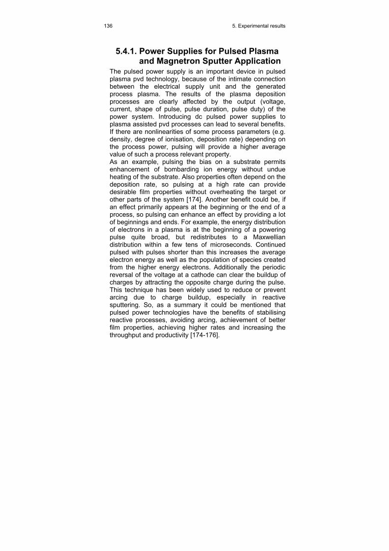
136 5. Experimental results
5.4.1. Power Supplies for Pulsed Plasma and Magnetron Sputter Application
The pulsed power supply is an important device in pulsed plasma pvd technology, because of the intimate connection between the electrical supply unit and the generated process plasma. The results of the plasma deposition processes are clearly affected by the output (voltage, current, shape of pulse, pulse duration, pulse duty) of the power system. Introducing dc pulsed power supplies to plasma assisted pvd processes can lead to several benefits. If there are nonlinearities of some process parameters (e.g. density, degree of ionisation, deposition rate) depending on the process power, pulsing will provide a higher average value of such a process relevant property. As an example, pulsing the bias on a substrate permits enhancement of bombarding ion energy without undue heating of the substrate. Also properties often depend on the deposition rate, so pulsing at a high rate can provide desirable film properties without overheating the target or other parts of the system [174]. Another benefit could be, if an effect primarily appears at the beginning or the end of a process, so pulsing can enhance an effect by providing a lot of beginnings and ends. For example, the energy distribution of electrons in a plasma is at the beginning of a powering pulse quite broad, but redistributes to a Maxwellian distribution within a few tens of microseconds. Continued pulsed with pulses shorter than this increases the average electron energy as well as the population of species created from the higher energy electrons. Additionally the periodic reversal of the voltage at a cathode can clear the buildup of charges by attracting the opposite charge during the pulse. This technique has been widely used to reduce or prevent arcing due to charge buildup, especially in reactive sputtering. So, as a summary it could be mentioned that pulsed power technologies have the benefits of stabilising reactive processes, avoiding arcing, achievement of better film properties, achieving higher rates and increasing the throughput and productivity [174-176].

5. Experimental results 137
The schematic of the power supply outlined in Fig.5.4.2 is a single phase pulse width modulated (PWM) design, which is very common in industrial units. In this design, the mains voltage is rectified to produce an uncontrolled dc voltage by the ac/dc converter. This voltage is delivered to the switching element, which is the heart of the power supply. The switching element produces a controlled alternating voltage and applies this voltage to a transformer. The transformer is not only used to provide isolation from the mains, but also to move the output voltage and current to the level required by the load. The output of the transformer is applied to a rectifier, which produces a dc output with ripple at the switching frequency. This ripple is reduced by a LC filter [175].
Fig.5.4.2: Block diagram of a switch mode power supply [175]
5.4.2. DC-PMS TiN process A standard planar dc magnetron source was supplied in this configuration with an additional dc pulse generator and a magnetic cylindrical plasma confining tube (Fig.5.4.3). The frequency of the dc pulse generator was varied in the range from dc to 250kHz generating 1296ns pulses. Experiments were carried out with Ti and Cr targets under Ar/N2 atmosphere (Ar=210sccm, N=30sccm) with total gas pressures between 1*10−3mbar - 7*10−3mbar. The electrical power input of the generator was between 70-210W depending on the process variations. The following investigations on a dc pulsed sputtering process were to clarify the potential capabilities of pulsed processing for the technology of TiN and CrN coating depositions.

138 5. Experimental results
Fig.5.4.3: Schematic of a reactive dc pulsed magnetron sputtering plant with a magnetic cylindrical plasma confining tube
Fig.5.4.4: Energy spectrum of the Ar+ ions of a magnetically forced dc pulsed TiN plasma of a planar magnetron. As can be seen, with increasing frequency of the current regulated generator the amount and the energy of the ions are strongly increased.
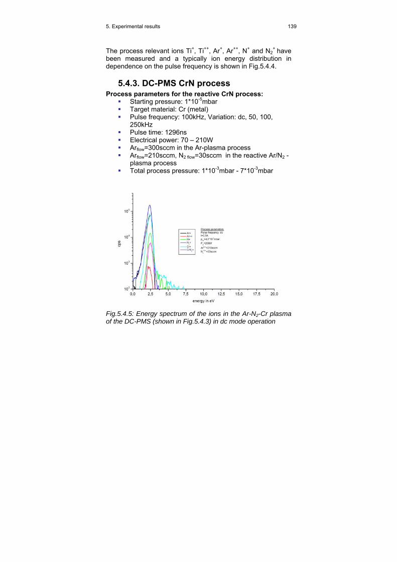
5. Experimental results 139
The process relevant ions Ti+, Ti++, Ar+, Ar++, N+ and N2+ have
been measured and a typically ion energy distribution in dependence on the pulse frequency is shown in Fig.5.4.4.
5.4.3. DC-PMS CrN process Process parameters for the reactive CrN process:
Starting pressure: 1*10-5mbar Target material: Cr (metal) Pulse frequency: 100kHz, Variation: dc, 50, 100,
250kHz Pulse time: 1296ns Electrical power: 70 – 210W Arflow=300sccm in the Ar-plasma process Arflow=210sccm, N2 flow=30sccm in the reactive Ar/N2 -
plasma process Total process pressure: 1*10-3mbar - 7*10-3mbar
Fig.5.4.5: Energy spectrum of the ions in the Ar-N2-Cr plasma of the DC-PMS (shown in Fig.5.4.3) in dc mode operation

140 5. Experimental results
Fig.5.4.6: Energy spectrum of the ions in the Ar-N2-Cr plasma of the DC-PMS (shown in Fig.5.4.3) process at f=100kHz
Fig.5.4.7: Energy spectrum of the Cr+ ions in the Ar-N2-Cr plasma of the DC-PMS (shown in Fig.5.4.3) in dc and pulsed mode operation
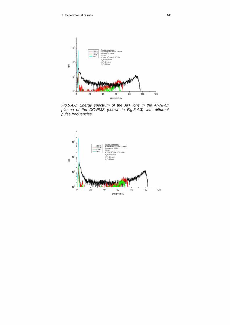
5. Experimental results 141
Fig.5.4.8: Energy spectrum of the Ar+ ions in the Ar-N2-Cr plasma of the DC-PMS (shown in Fig.5.4.3) with different pulse frequencies

142 5. Experimental results
Fig.5.4.9: Energy spectrum of the N2+ ions in the Ar-N2-Cr plasma of the DC-PMS (shown in Fig.5.4.3) with different pulse frequencies
5.4.4. DC-PMS Ta2O5 process In the following configuration an industrial Sputtercoater (Edwards) with a magnetron sputter source was operated in connection with a dc pulsed power generator (Advanced Technologies) [80].
PPM 421 Smart Probe
Magnetron target
Race track
Sputtercoater Edwards 500
62 mm
500mm
Fig. 5.4.5: Schematic of the plasma measurements in a dc pulsed magnetron sputtering process, showing the position of the plasma monitoring system PPM421 (Inficon) and the Langmuir probe system (Scientific Instruments)
Fig. 5.4.6: Schematic of the applied pulses

5. Experimental results 143
Fig.5.4.7: Ion energy distribution of the Ar+ ions in dependence on the pulse frequency in a dc pulsed magnetron sputter process using a dielectric Ta2O5 target From such plasma measurements (ion energy distribution) the total energy input into a growing deposit can be evaluated. The calculation of the total energy input into the growing film produced by bombardment with ions of energies from a corresponding energy distribution of the involved ions, can be performed according to:
∫∑ ⋅= dxxfxEIonen
inpution )(
with x: kinetic energy of the ion, f(x): amount of ions with the kinetic energy x and input
ionE : sum of the weighted area of the ion energy distribution of the process relevant ions

144 5. Experimental results
Fig.5.4.8: Calculated total energy input into the growing film by bombarding ions From Fig.5.4.8 can be seen that the possible energy input into a growing film with increasing pulse frequency approaches a maximum value. Experimentally it could be shown that applying a pulsed voltage to the sputter target, the energy spectrum of the coating material ions particularly become bimodal in nature, with a sharp low energy peak and an additional higher energy peak. With increasing frequency, of the lower energy peak decreases in amplitude whereas that of the higher energy increases what can be seen in Fig.5.4.4 and Fig.5.4.7. The growing amplitude of the high energy peak, with rising frequency, results from the relative increase in the percentage of the total ion flux that arrives to the substrate plane with a higher energy in the range of Ei +/- ΔE.

5. Experimental results 145
5.4.5. Summary of the dc magnetron sputter process Mass spectrometric measurements during sputtering have shown that at about 10-2mbar gas pressure the coating material ions arrived at the substrate with only 2–3eV. TiN films formed under such pressure had lower adherence, hardness and abrasion resistance. However, films produced under such conditions have adequate quality for use in decorative and protective coatings. A further increase of the gas pressure to about 10-1mbar reduced the particle energy in the investigated sputtering variants so drastically that these techniques can not be used practically under such conditions. The magnetically forced and medium frequency pulsed biased dc magnetron sputter deposition variants, operating in the 10-3 mbar gas pressure range, showed a relatively large amount of single and double charged positive ions with kinetic energies up to 55eV and 95eV, as consequence of the applied modifications. However, increasing the total gas pressure up to 10-1mbar decreases the kinetic energy of the involved particles so strongly that no high performance films could be deposited under such conditions.

146 5. Experimental results
5.5. PLAD – Pulsed Laser Ablation Deposition
The PLAD process has been characterised using different diagnostic tools, such as Optical Emission Spectroscopy OES with Intensified Charge Coupled Device ICCD, and Quadrupol Mass Spectrometry. A schematic view of the experimental arrangement for mass spectrometry analysis is shown in Fig.5.5.2 below. As indicated, the sensor head replaces the substrate at the same position with respect to the plume. The following pictures show the PLAD system at University of Potenza [81].
Fig.5.5.1: PLAD configuration at University of Potenza

5. Experimental results 147
Fig.5.5.2: Experimental set up for mass spectrometry analysis of the plume as carried out by University of Roma, University of Potenza and University of Innsbruck Process parameters for deposition:
Vacuum chamber equipped with quartz window for laser beam inlet and in situ optical analysis
Heatable substrate holder (up to 800°C) Rotating target support (TiC targets 99% - Cerac) Lowest pressure: 1,5*10
-6 mbar Laser source: Nd-YAG Laser (frequency doubled) λ=532nm, t=10ns, 10Hz repetition rate Incidence angle = 45° Substrate distance: 2,5cm Laser fluence range: 0 to 15J/cm
-2 Some previous measurements were carried out on the PLAD process at University of Potenza (Dr. Teghil, Dr. Santagata) with optical spectroscopy and data presented in following pictures
Intensified charge coupled device – ICCD (Princeton camera)
Spatial and temporal resolution: 150mm and 5nsAblation rate: measured from the weight loss of the targets (108.000 laser shots)

148 5. Experimental results
[81]
Fig. 5.5.3: For the TiC process the diagram shows a non-linear behaviour that can be divided in three different zones (I, II, III), probably originated from different ablation processes [81].
Fig. 5.5.4: Temporal evolution of laser plume: ICCD intensity contour patterns showing the temporal evolution of TiC plumes, obtained with incremental delays of 100ns starting from 10ns after laser pulse. The grid depth is 3mm [81].
I I I

5. Experimental results 149
Fig. 5.5.5: Mass spectrometer measurement of TiC process: At lower laser fluence an intensive dicarbide peak is present in the TiC spectrum. At higher fluence the only recorded feature is the metal peak [81].
Fig. 5.5.6: Picture of TiC laser plume: Picture was recorded at 4J/cm² taking the intensity profile along the longitudinal direction, averaged inside the dashed box [81].

150 5. Experimental results
0,0 5,0x10⁶ 1,0x10⁷ 1,5x10⁷ 2,0x10⁷
0
2000
4000
6000
8000
10000
12000
14000
16000
18000
20000
22000
24000
Ti vcm= 1.43x106 cm s-1
Ti+ vcm= 2.48x106 cm s-1
Inte
nsity
(a.u
.)
v (cm/s)
0,0 5,0x10⁶ 1,0x10⁷ 1,5x10⁷ 2,0x10⁷
0
2500
5000
7500
10000
12500
15000
17500
20000
22500
25000
C+ vcm= 4.66x106 cm s-1
Ti++ vcm= 7.26x106 cm s-1
Inte
nsity
(a.u
.)
v (cm/s)
Fig. 5.5.7: Velocity distribution of different particles in the TiC process: (actual measurements from the TiC process taken after the bilateral meeting in Potenza). The graphic has been collected by accumulating data from 100 shots having all the same delay. In order to get the speed distribution we have kept fixed the optical fiber position (5mm far from the target) and collected the emission intensity of each species at different delays, that means different speeds.

5. Experimental results 151
2,4x10⁴ 2,6x10⁴ 2,8x10⁴ 3,0x10⁴ 3,2x10⁴ 3,4x10⁴ 3,6x10⁴ 3,8x10⁴ 4,0x10⁴
-40
-30
-20
-10
0TiC Ablation; F = 1.2 J cm-2
Te= 9000 K
(Y) = A + B * XParameter Value Error------------------------------------------------------------A -27,22186 2,09507B -1,60268E-4 6,91886E-5------------------------------------------------------------R SD N P-------------------------------------------------------------0,52637 1,29384 16 0,03621------------------------------------------------------------
ln (I
21λ 21
/g2A
21)
E2 (cm-1)
2,4x10⁴ 2,6x10⁴ 2,8x10⁴ 3,0x10⁴ 3,2x10⁴ 3,4x10⁴ 3,6x10⁴ 3,8x10⁴ 4,0x10⁴
-40
-30
-20
-10
0
(Y) = A + B *XParameter Value Error------------------------------------------------------------A -26,92725 1,69183B -1,49416E-4 5,58717E-5------------------------------------------------------------R SD N P-------------------------------------------------------------0,58148 1,04481 16 0,01815------------------------------------------------------------
Te= 9600 KTiC Ablation; F = 11.0 J cm-2
ln (I
21λ 21
/g2A
21)
E2 (cm-1)
Fig. 5.5.8: Local thermodynamic equilibrium

152 5. Experimental results
Best TiC coatings have been achieved with the following process parameters:
Temp.: 25°C Laser power: 10J/cm2 Distance substrate – target: 5cm TiC coatings were deposited onto polished steel samples – 1cm2
Dependences:
Quality of TiC coating is strictly dependent on the distance Coatings are homogenious and reproduceable at a distance of 8cm
At distances lower than 8cm the coatings are not homogenious over the whole sample area
From the experimentally results it can be seen that the pulsed laser ablation deposition (PLAD) method is based on physical processes, arising from the impact of high power pulsed laser radiation on solid targets and leading to the removal of partially ionised material (plasma) from the impact zone [82]. The properties of the deposited films depend strongly on the deposition characteristics and can be controlled by changing the process parameters. Formation of the plasma flux characteristics in the laser plasma method starts with laser radiation interaction with the target. At pulsed laser flux densities of 105-108Wcm-2, as used in PLAD, the quasi stationary target evaporation regime is reached, where the temperature of the evaporating surface T0 remains constant. A specific feature of the PLAD fluxes is their high degree of ionisation and high kinetic ion energy, which depend on experimental conditions, such as laser radiation flux density, wave length, target material, and the temporal shape of the laser pulse [82]. At nanosecond pulse duration the energy spectrum of the ions is in the region of 0eV to 2000eV with a mean energy of 100eV to 400eV, depending on the experimental conditions. The ionisation degree of the plasma is between 10% and 70% and depends strongly on the energetic and spectral laser parameters. The neutral component of the plasma flux has relatively low mean energy (∼10eV) [82] and comprises 30% to 90% of the evaporated

5. Experimental results 153
material, depending on the thermophysical properties of the target and on the laser parameters. Growth of films by PLAD is a process that depends on many factors, such as density, energy, ionisation degree, type of condensing particles, as well as the temperature and physiochemical properties of the substrate [2,3]. The two main thermodynamic parameters that determine to a great extent the growth mechanism are the substrate temperature T and the supersaturation m
eRRkTm ln=
where k is the Boltzmann constant, R is the actual deposition rate and Re is its equilibrium value at temperature T. At the extremely high deposition rates in PLAD, the plasma flux supersaturation reaches the value of 105 J mol-1, which is many order of magnitude higher than in the conventional stationary deposition techniques. Thermal and kinetic energy of the plasma particles can significantly influence some film properties. Depending on the energy of the particles, several specific cases can be distinguished [69, 70]:
1. The thermal energy of the evaporated particles is much less than the dissociation energy of the molecules of the target material. This regime can be realised with relatively long laser pulses (∼10-3s) and low fluences (∼105Wcm-2). These conditions are suitable for obtaining stoichiometric films of poly-component materials with high energy dissociation, for example oxides.
2. In the case that the thermal energy of the particles is of the order of the dissociation energy, the target material is partially or completely dissociated and the dissociation energy is released on the substrate surface in the process of atom to molecule association. This regime concerns most of the poly-component semiconductors and may be also realised with long laser pulses and flux densities of approximately 105-106 Wcm-2.

154 5. Experimental results
3. The kinetic energy of the particles is the order of the defect-formation energy (app. 20eV). Irradiation of monocrystalline substrates with particles of this energy produces a network of radiative defects (vacancies), which are additional crystallisation centers. This process allows epitaxial growth of films at moderate mobility of the adsorbed atoms, that is, at lower temperatures as compared to other methods.
4. At higher laser fluences (108-109 Wcm-2) the laser produced plasma contains a significant amount of high energetic particles (100-2000eV). Ions of this energy produce in a thin surface layer (∼30A) individual vacancies, which then diffuse deep into the substrate and recombine over a time of ∼10-8s with almost no worsening of the crystal properties. It is well known, that diffusion of adatoms in solids occurs mainly in unoccupied nodes of the crystal lattice (vacancies), and the high temperature at which this diffusion takes places is needed to ensure that a maximum number of atoms escape from the lattice nodes. The number of plasma produced vacancies exceeds the equilibrium value for a given temperature by many orders of magnitude. This results in an increase of the diffusion coefficient to the same extent. Radiation stimulated diffusion ensures excellent adhesion of the deposited films, even at very low substrate temperatures [69].
The influence of the main growth parameters (substrate temperature and deposition rate) on the stoichiometry and structure of laser plasma synthesized thin film compounds has been studied on the basis of lead salts [5]. Investigations of the structural properties and the stoichiometry of the layers, deposited at different technological conditions (substrate temperature, distance target-substrate, laser pulse energy) has shown that there is a critical substrate temperature Tc, below which the structure of the films is not completely monocrystalline and the film composition deviates significantly from the stiochiometric one. So the substrate temperature is very important not only for the film structure but also for the preservation of the stoichiometry of the deposited polycompound films.

5. Experimental results 155
Fig. 5.5.9: Absolute ionisation degree in a Ti-plasma flux dependent on the laser energy density [69] The previous data, shown in Fig.5.5.3 to Fig.5.5.8, give us some insight about the ablation process mechanism of the TiC considered here [81]. Concerning the vaporisation of TiC it was found a non-congruent process accompanied by the reaction Ti + 2C = TiC2 in the zone I, indicating a thermal evaporation at equilibrium conditions. In the remaining zones the vaporisation process is congruent (Fig.5.5.3). This behaviour can be explained with the physical-chemical properties of solid TiC [83, 84]:
Young’s modulus: 447 GN m-2 Micro hardness: 30000 MN m-2 Debye’s temperature: 542,4 K Enthalpy of formation: -184,6 kJ mol-1
The formation of TiC2 in the plume can be justified and a high laser fluence is necessary to obtain a congruent TiC vaporisation. The high energy of the TiC plume (due to the presence of a large amount of ionised particles) could also justify the deposition of crystalline films at room temperature. PLAD process conditions, that give the possibility to realise high quality films, are those of zone II (Fig.5.5.3) in which the films present high crystallinity and compactness.

156 5. Experimental results
5.6. ASD – Arc Source Deposition
5.6.1. General description The application of the cathodic arc to the deposition of thin film materials has primarily arisen through the attractive characteristics of the emission products for thin film growth. From the point of view of film deposition, the important properties of the particles are: charge, degree of ionisation and energy distribution. Several groups have measured the charge state and degree of ionisation [85, 86]. The charge multiplicity was found range from +1 to +4 and higher. The ionised fraction f of the emitted particles is a strong function of the cathode material with values ranging from 12-15% for Cd and 80-100% for Mg [87]. The measured values for f are also dependent upon the residual gas pressure, for example a value of 68% for Ti under high vacuum conditions were reported and 85% for a background nitrogen pressure of 1,0 -.1,5*10-³mbar during the deposition of TiN [88]. The energy of the ions arriving at the substrate may be increased simply by the application of a negative bias to accelerate the positive ions. However, at a sufficiently high negative bias, the self-sputtering yield is such that no net deposition takes place anymore (>-400V for Zr, -600V for Ti and -1500V for Ti at 2*10-4mbar N2 [89]. When the energy of the arc evaporated ions is increased by biasing the substrate, the incident ion flux may also be diffused into the substrate by radiation-enhanced processes which are also assisted by the increase in surface temperature. The depth of penetration of particles under these conditions is significant. For example, in the case of a 1kV bias on steel during Ti deposition, the range of Ti is approximately 1μm. The net result of such processes is that the film-substrate interface is increased and the adhesion is improved greatly [90]

5. Experimental results 157
5.6.2. Arc source plant and process parameters
An industrial arc source plant (from IonBond Ldt., UK), with the possibility to apply the chamber with up to 18 arc sources, was used for the plasma analysis of an arc source ion plating process. The plasma monitoring system PPM421 (quadrupol mass spectrometer with additional cylindrical energy analyser) and a Langmuir probe system (SmartProbe, Scientific systems) were connected to the plant to investigate the kind and amount of ions, their energy distributions, the densities of charged particles and the electrical potentials in dependence on the process parameters.
Fig.5.6.1: Arc source unit (left) and arc source deposition system at IonBond Consett, UK The plasma measurements were carried out on various Ti and Cr arc source processes using a Ti or Cr target together with different process gases (Ar, CH4, C2H4, C4H10, C2H2, N2) at a total pressure of 3mT. Two different types of targets were used: a standard (plane surface) and a special RGCA (reactive gas controlled arc) design from IonBond Ldt. with a cone shaped surface and a gas inlet hole in the middle of the target.

158 5. Experimental results
Fig. 5.6.2.: Schematic of an arc source unit Process parameters and variations: Ti target Standard arc source process
• Vacuum – no additional working gas
• Ar - 3mT • CH4 – methan – 3mT • C2H4 – ethylene – 3mT • C4H10 – buthan – 3mT • C2H2 – acethylen – 3mT
RGCA - reactive gas controlled arc source process
• Ar - 3mT • CH4 – methan – 3mT • C2H4 – ethylene – 3mT • C4H10 – buthan – 3mT • C2H2 – acethylen – 3mT • N2 – nitrogen – 3mT
Process parameters and variations: Cr target Standard arc source process
• Vacuum – no additional working gas
• N2 – nitrogen – 3mT • C2H4 – ethylene – 3mT • C2H2 – acethylen – 3mT
RGCA - reactive gas controlled arc source process
• N2 – nitrogen – 3mT • C2H4 – ethylene – 3mT • C2H2 – acethylen – 3mT

5. Experimental results 159
5.6.3. Arc source plant and plasma measurement setup
Fig. 5.6.3: Pictures of arc source plant and applied plasma measurement systems at Ionbond, Consett, UK

160 5. Experimental results
Fig. 5.6.4: Principle setup and configuration of the plasma analysing systems

5. Experimental results 161
Fig. 5.6.5: Picture with distances in the plasma measurements Two different targets shapes were investigated in the different ASD processes: a standard arc target with a planar surface geometry and a special designed RGCA (reactive gas controlled arc) target with a cone shaped surface geometry.
Fig. 5.6.6: RGCA (reactive gas controlled arc) target from Ionbond, UK
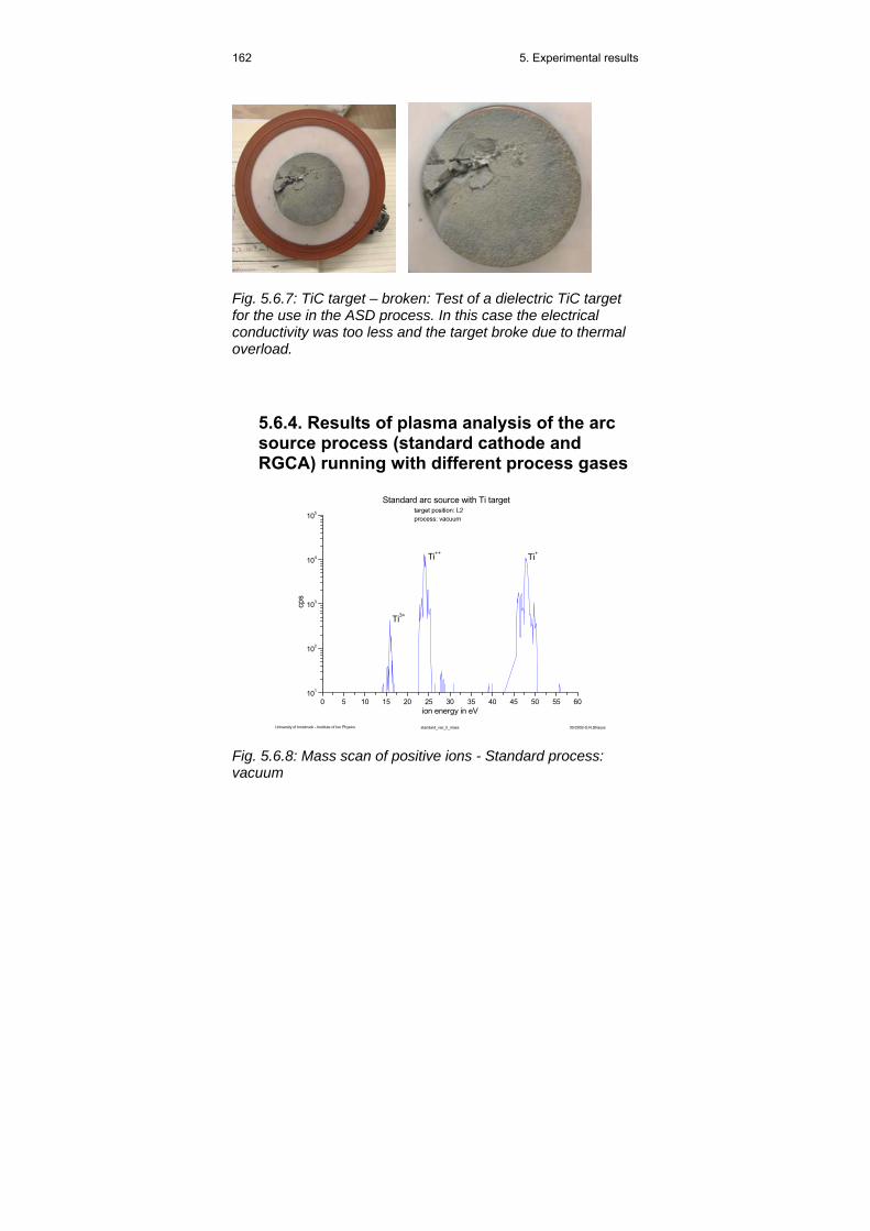
162 5. Experimental results
Fig. 5.6.7: TiC target – broken: Test of a dielectric TiC target for the use in the ASD process. In this case the electrical conductivity was too less and the target broke due to thermal overload.
5.6.4. Results of plasma analysis of the arc source process (standard cathode and RGCA) running with different process gases
0 5 10 15 20 25 30 35 40 45 50 55 60101
102
103
104
105
Ti3+
Ti++ Ti+
standard_vac_ti_mass 05/2002-G.N.StraussUniversity of Innsbruck - Institute of Ion Physics
target position: L2process: vacuum
Standard arc source with Ti target
cps
ion energy in eV
Fig. 5.6.8: Mass scan of positive ions - Standard process: vacuum

5. Experimental results 163
0 20 40 60 80 100
103
104
105
106
standard_vac_ti_energy 05/2002-G.N.StraussUniversity of Innsbruck - Institute of Ion Physics
target position: L2process: vacuum
Standard arc source with Ti target
amu 16 - Ti3+
amu 24 - Ti2+
amu 48 - Ti+
cps
ion energy in eV
Fig.5.6.9: Energy scans of positive ions - Standard process: vacuum
0 20 40 60 80 100
103
104
105
106
standard_ar_ti_energy 05/2002-G.N. StraussUniversity of Innsbruck - Institute of Ion Physics
target position: L2process: Ar 3mT
Standard arc source with Ti target
amu 16 - Ti3+
amu 24 - Ti2+
amu 48 - Ti+
cps
ion energy in eV
Fig.5.6.10: Energy scans of positive ions - Standard process: Ar pressure = 3mT

164 5. Experimental results
0 20 40 60 80 100
103
104
105
106
standard_ch4_ti_energy 05/2002-G.N.StraussUniversity of Innsbruck - Institute of Ion Physics
target position: L2process: CH4 3 mT
Standard arc source with Ti target
amu 16 - Ti3+
amu 24 - Ti2+
amu 48 - Ti+
amu 49 amu 50
cps
ion energy in eV
Fig.5.6.11: Energy scans of positive ions - Standard process: CH4 pressure = 3mT
0 20 40 60 80 100
103
104
105
106
standard_c2h2_ti_energy 05/2002-G.N. StraussUniversity of Innsbruck - Institute of Ion Physics
target position: L2process: C2H2 3mT
Standard arc source with Ti target
amu 12 - Ti4+
amu 24 - Ti2+
amu 48 - Ti+
cps
ion energy in eV
Fig.5.6.12: Energy scans of positive ions - Standard process: C2H2 pressure = 3mT

5. Experimental results 165
0 20 40 60 80 100
103
104
105
106
standard_c4h10_ti_energy 05/2002-G.N. StraussUniversity of Innsbruck - Institute of Ion Physics
target position: L2process: C4H10 3mT
Standard arc source with Ti target
amu 16 - Ti3+
amu 24 - Ti2+
amu 48 - Ti+
amu 46 amu 50
cps
ion energy in eV
Fig.5.6.13: Energy scans of positive ions - Standard process: C4H10 pressure = 3mT
0 20 40 60 80 100
103
104
105
106
standard_ti_energy_overview 05/2002-G.N.StraussUniversity of Innsbruck - Institute of Ion Physics
energy distribution of Ti+ ions with different process parametersStandard arc source with Ti target
vacuum argon CH4 C2H4
C4H10
C2H2
cps
ion energy in eV
Fig.5.6.14: Energy scans of Ti+ ions - Standard process: Overview of different process gases

166 5. Experimental results
0 20 40 60 80 100
103
104
105
106
standard_ti_energy_arccurrent 05/2002-G.N.StraussUniversity of Innsbruck - Institute of Ion Physics
energy distribution of Ti+ ions with different arc currentsStandard arc source with Ti target
Iarc=60A Iarc=90A
cps
ion energy in eV
Fig.5.6.15: Energy scans of Ti+ ions - Standard process: Different arc currents
0 20 40 60 80 100
103
104
105
106
107
rgca_ar_ti_energy 05/2002-G.N. StraussUniversity of Innsbruck - Institute of Ion Physics
target position: L2process: Ar 3mT - inlet through chamber
RGCA arc source with Ti target
amu 24 - Ti2+
amu 48 - Ti+
cps
ion energy in eV
Fig.5.7.16: Energy scans of Ti+ ions - RGCA process: Ar pressure = 3mT

5. Experimental results 167
0 20 40 60 80 100
103
104
105
106
rgca_ch4_ti_energy 05/2002-G.N. StraussUniversity of Innsbruck - Institute of Ion Physics
target position: L2process: CH4 3mT - inlet through target
RGCA arc source with Ti target
amu 12 - Ti4+
amu 24 - Ti2+
amu 48 - Ti+
cps
ion energy in eV
Fig.5.6.17: Energy scans of Ti+ ions - RGCA process: CH4 pressure = 3mT
0 20 40 60 80 100
103
104
105
106
rgca_c2h2_ti_energy 05/2002-G.N. StraussUniversity of Innsbruck - Institute of Ion Physics
target position: L2process: C2H2 3mT - inlet through target
RGCA arc source with Ti target
amu 12 - Ti4+
amu 24 - Ti2+
amu 48 - Ti+
cps
ion energy in eV
Fig.5.6.18: Energy scans of Ti+ ions - RGCA process: C2H2 pressure = 3mT

168 5. Experimental results
0 20 40 60 80 100
103
104
105
106
rgca_c4h10_ti_energy 05/2002-G.N. StraussUniversity of Innsbruck - Institute of Ion Physics
target position: L2process: C4H10 3mT - inlet through target
RGCA arc source with Ti target
amu 12 - Ti4+
amu 24 - Ti2+
amu 48 - Ti+
cps
ion energy in eV
Fig.5.6.19: Energy scans of Ti+ ions - RGCA process: C4H10 pressure = 3mT
0 20 40 60 80 100
103
104
105
106
107
compare_sources_ar 05/2002-G.N.StraussUniversity of Innsbruck - Institute of Ion Physics
energy distribution of Ti+ and Ti++ ions in the Ar-processComparison of arc sources (standard-rgca) with Ti target
Ti+ - standard source
Ti+ - rgca source
Ti++ - standard source
Ti++ - rgca source
cps
ion energy in eV
Fig.5.6.20: Energy scans of Ti+ ions – Comparison of Standard and RGCA process: Ar pressure = 3mT

5. Experimental results 169
0 20 40 60 80 100
103
104
105
106
compare_sources_c4h10 05/2002-G.N.StraussUniversity of Innsbruck - Institute of Ion Physics
energy distribution of Ti+ and Ti++ ions in the C4H10-processComparison of arc sources (standard-rgca) with Ti target
Ti+ - standard source
Ti+ - rgca source
Ti++ - standard source
Ti++ - rgca source
cps
ion energy in eV
Fig. 5.6.21: Energy scans of Ti+ ions – Comparison of Standard and RGCA process: C4H10 pressure = 3mT Table 5.6.1: Energy distribution of Ti+ and Ti++ ions in different arc processes
Process Ti+ Standard RGCA
Max in eV Range in eV Max in eV Range in eV Vac 50 30-70 --- --- Ar 35 10-65 30 0-45 CH4 30 0-50 60 25-110 C2H2 50 25-80 40 25-90 C4H10 30 15-50 60 30-110
Process Ti++ Standard RGCA Max in eV Range in eV Max in eV Range in eV
Vac 30 25-55 --- --- Ar 35 10-40 30 0-45 CH4 30 0-35 60 25-110 C2H2 30 25-50 25 0-40 C4H10 30 5-40 30 30-60

170 5. Experimental results
-5,0-4,5-4,0-3,5-3,0-2,5-2,0-1,5-1,0-0,50,00,51,01,52,02,53,0
VacC2H290 A
C2H260 AC4H10_01
Position:L2 Target: Titan
ArCH4C4H10C2H4
Vf Vp kTepo
tent
ial (
V) /
ele
ctro
n en
ergy
(eV)
Fig.5.6.22: Floating potential, plasma potential and electron energy in the different standard arc processes The plasma measurements at IonBond (UK) were carried out on various Ti and Cr arc source processes using a Ti or Cr target together with different process gases (Ar, CH4, C2H4, C4H10, C2H2, N2) at a total pressure of 3mT. It was also tried to test a TiC target, but it broke due to problems with the bonding of the target (Fig.5.6.7). In the Ti arc source processes two different types of target were used: a standard (plane surface) and a special RGCA (reactive gas controlled arc) design from IonBond (Fig.5.6.6) with a cone shaped surface and a gas inlet hole in the middle of the target. Plasma analysis were done with a plasma monitoring system PPM421 (Inficon) which consists of a quadrupol mass spectrometer and a additional cylindrical energy analysing unit. With this system it is possible to detect the different ionised particles in the plasma and to measure their energy distribution. Additional to the plasma monitoring system a Langmuir probe system (Smartprobe from Scientific Systems) has been used to measure the densities and potentials in the arc source plasmas.

5. Experimental results 171
5,0x10⁹
1,0x10¹⁰
1,5x10¹⁰
2,0x10¹⁰
2,5x10¹⁰
3,0x10¹⁰
3,5x10¹⁰
4,0x10¹⁰
4,5x10¹⁰
5,0x10¹⁰
Position:L2 Target: Titan
VacC2H290 A
C2H260 AC4H10_01
ArCH4C4H10C2H4
ne ni
dens
ity (c
m-3)
109
1010
1011
L2 Titan RGCA
N2ArCH4C2H10C2H4
C2H2
ne ni
Dic
hte
(cm
-3)
Fig.5.6.23: Top: Ion and electron density in the different standard arc processes, Bottom: Ion and electron density in the different rgca arc processes In general the measurements showed the high state of ionisation (single and multiple ionised particles) of the target particles in the arc source process (Fig.5.6.8). The energy distribution of the ions is in the range from 0 to 100eV depending on the process (Ar, CH4, C2H4, C4H10, C2H2, N2)

172 5. Experimental results
and the investigated particle (Ti+, Ti2+, Ti3+) shown in Fig.5.6.9–5.6.21. In general the RGCA target produces a larger amount of ions and ions with a larger energy distribution up to 110eV compared with the standard target with maximum energies up to 80eV (Fig.5.6.20 and 5.6.21). Table 5.6.1 gives an overview about the two different targets (standard and RGCA) showing the energy range and maximum of energy distribution of Ti+ and Ti++ in the different arc source processes. The floating potential is in the range from –2V to –4V depending on the reactive gas in the process, the plasma potential was measured at +2,5V and the electron temperature kTe is 1,5V nearly not changing with the different gases (Fig.5.6.22). The density of charged particles is in the range from 5*109cm-3 to 3*1010cm-3 (Fig.5.6.23).
5.6.5. Results of plasma analysis of a TiN arc source process
The arrangement for the plasma analysis of a standard planar arc source is shown in Fig.5.6.24 [92]
Fig.5.6.24: Schematic of an arc source ion plating plant with the static standard substrate holder (FEM, Schwäbisch-Gmünd, Germany).

5. Experimental results 173
Fig.5.6.25: Energy spectra of the Ti+ ions in the reactive TiN arc source ion plating process (Fig.5.80) at various N2 gas pressures (1*10-3 mbar to 1*10-1 mbar) at constant arc current (Ti cathode distance 20cm). It is remarkable how many energetic Ti+ ions were found even at 10-1 mbar gas pressure In order to measure the in situ substrate current density in the cathodic arc source deposition arrangement, in some experiments, the substrate holder was replaced by an ion current probe. In these experiments it was found that for high pressure arc deposition the ion current density varied strongly in the initial period of evaporation. Under the used conditions the high substrate current density of 4mAcm-2 in the beginning decreased rapidly and finally reached a balance value of about 2mAcm-2 for longer process times (Fig.5.6.26 and 5.6.27).
0 20 40 60 80 100 120102
103
104
105
106
107 Process parameters:Iarc=85AArc target Ti (distance=20cm)PN2 variable
ptot=1*10-3mbar
ptot=1*10-2mbar
ptot=1*10-1mbar
cps
energy in eV

174 5. Experimental results
Fig.5.6.26: Substrate ion current density distributions at a N2 pressure of 5*10-3mbar (85 A arc current, ion probe position (Faraday Cup) parallel to target plane).
Fig.5.6.27: Substrate ion current density distributions at a N2 pressure of 1*10-1mbar (85 A arc current, ion probe position (Faraday Cup) parallel to target plane).
0 2 4 6 8 10 12 14 160
2
4
6
8
10
12
14
16
18
distance: source-substrate 15 cm 20cm 25cm
pN2=1*10-1mbar
subs
trate
cur
rent
den
sity
in m
A/cm
2
perpendicular distance to central axisbetween source-substrate
0 2 4 6 8 10 12 14 160
2
4
6
8
10
12
14
16
18pN2=5*10-3mbar
distance: source-substrate 15 cm 20cm 25cm
subs
trate
cur
rent
den
sity
in m
A/cm
2
perpendicular distance to central axisbetween source-substrate

5. Experimental results 175
Cathodic arc deposition, in the same gas pressure range of 10-3mbar, showed a very high number of such ions with energies up to more than 100eV, depending on the value of the applied current. However, at constant distance between source and substrate the higher gas pressure increases also the number of energy reducing collisions of the coating material vapour-species with the gas molecules. The arc source process, even when performed at high gas pressures of 10-1mbar, showed a remarkable amount of ions with energies up to 75eV resulting in high performance TiN and CrN films of quite proper 3D homogeneity [92].
5.6.6. Summary of the arc source process Cathodic arc deposition, in the gas pressure range of 10-3
mbar, showed a very high number of ions with energies up to more than 100eV, depending on the value of the applied current. However, at constant distance between source and substrate the higher gas pressure increases also the number of energy reducing collisions of the coating material vapour species with the gas molecules. The arc source process, even when performed at high gas pressures of 10-1mbar, showed a remarkable amount of ions with energies up to 75eV resulting in high performance TiN and CrN films of quite proper 3D homogeneity. The arc source process, even when performed at high gas pressures of about 10-1mbar, showed a remarkable amount of ions with energies up to 75eV resulting in high performance TiN films over the full range of conditions evaluated. By operating at high pressure of about 10-1mbar the arc source technique is able to increase film thickness uniformity up to 3 times with respect to the traditional coatings if the samples are mounted in a way that they do not influence each other. For lowering the coating costs a combination of a more consistent plasma cleaning at higher gas pressures, started during pump-down, together with enhanced desorption in conjunction with a Poly-Cold pump produced a remarkable decrease of the pump-down time. Also eliminating pre-heating by pre-cleaning of the substrates prior to deposition by performing plasma ion cleaning while pumping, shortened the

176 5. Experimental results
pre-deposition time. This means, it became possible to reduce the total process-time by up to 50%. With these investigations and results it could be demonstrated that the plasma monitoring and characterization of the individual plasma processes deliver a base for further industrial developments and optimizations of low-temperature high-pressure plasma coating processes [113-118].
5.7. Summary of the experimental results
5.7.1. General statements about the influence of particle energies on film formation in different PVD processes
In coating processes without plasma assistance, the mode of nucleation and film growth is mainly determined by the thermo-chemistry of the substrate and film materials and the temperature of the system. Additionally, the rate of deposition, film thickness, and angle of incident are important [2]. These processes lead to island (Volmer-Weber), or layer-by-layer (Frank-van der Merve), or mixed layer-island (Stranski-Krastanov) growth. The effect of temperature on microstructure can be illustrated by structural zone diagrams [2, 167]. By the addition of plasma and ion assistance, or energetic condensation, chemical activity is dramatically increased. In the simplest case, considering dc-sputtering, Thornton [168] developed his well-known structural zone diagram that includes a pressure axis, there the additional pressure value is an indirect measure for the energy of assisting argon ions. In the various PVD process technologies like thermal evaporation, dc-sputtering, dc-pulsed sputtering, ion plating or arc source deposition, very different kinetic energies of the coating and/or gas materials can be observed. For example in simple evaporation the kinetic energies of the particles is in the range from 0.05 to 0.1eV, in DC Magnetron Sputtering from 1 and 15eV, in DC pulsed Sputtering up to some tens of

5. Experimental results 177
eV and in Ion plating and Arc Source Deposition up to 100eV and more. The film property modifications by ion bombardment are mainly caused by momentum transfer from the ions to the film atoms. The collisional effects due to the bombardment of energetic particles during film deposition produce a large variety of positive effects on properties in the growing film. These effects can appear as structural and morphological modifications, changes in density and chemical composition and related film properties [169]. Incident ions provide additional energy to surface atoms, which effectively leads to higher surface mobility, thereby aiding surface atoms to find energetically preferred locations. Recently, special interest is in low energy ions, i.e., ions of hyperthermal energy yet still low enough to not cause ion damage. In absolute units, this is the range of about 1eV-30eV. Low energy treatment is sufficient to remove weakly bounded surface atoms, especially water that is always present unless the process is done at very high temperature or in ultra-high vacuum (UHV). At somewhat higher energies, up to a few 100eV, shallow implantation (subplantation) will occur, often associated with film densification, increased hardness and Young’s modulus, high compressive stress and reduced roughness. Ion bombardment of crystalline films will cause heavy ion damage and in extreme case will get fully amorphous [170] for some materials and texture changes for others [171]. At even higher energies, greater than 500eV, the rate of sputtering of the surface will exceed the rate of deposition, effectively prohibiting film growth. This range can be characterised as an etch mode, which is important for surface preparation and patterning processes. In the case of polymer substrates, ions of too high energy and/or too high dose lead to substrate damage by chain-scissoring [172]. Particle energies of a few keV are used to remove material and to produce shallow implant profiles, which is important to some semiconductor processing. Another example of a process in this energy range is plasma nitriding, where hard and inert nitride phases are formed in the near-surface region of steel or aluminium alloys [173].

178 5. Experimental results
Finally, at the very high end of the ion energy scale, ion implantation at 100s of keV or some MeV is done routinely, but these processes and applications are beyond the scope of this review and not to be further considered. Apart from ion bombardment, plasmas also offer utilization of their electron component, which is especially useful when positive charge on an insulating surface needs to be neutralized, or when the growing film needs to be heated without heating the bulk of the substrate [169]. As a summary it can be mentioned that the improvement of the performance of dielectric conventional reactive processes, even in activated environment, is limited. Ion and/or plasma assisted pvd processes like ion plating (RLVIP, APS), medium frequency magnetron sputtering (DC pulsed MSD), ion beam sputtering (IBSD) or arc source deposition (ASD), work much more effective [196-199].
5.7.2. Overview of the ion energy in the investigated pvd processes
Table 5.7.1: Mass spectrometric data of the ions obtained in the different reactive deposition processes
Process
Parameters
α
Ions
Energy range
Low pressure TiN deposition pN2 = 4*10-3mbar Arc current = 85A Substrate bias = floating
high
N+ Ti+ Ti++ N2
+ TiN+
0 – 80eV 0 –110eV 0 – 80eV 0 – 50eV 0 –45eV
Medium pressure TiN deposition pN2 = 1,3*10-2mbar Arc current = 85A Substrate bias = floating
high
N+ Ti+ Ti++ N2
+ TiN+
0 – 80eV 0 –110eV 0 – 80eV 0 – 40eV 0 –35eV
ASD
Reactive arc source deposition
High pressure TiN deposition pN2 = 1*10-1mbar Arc current = 85A Substrate bias = floating
high
N+ Ti+ Ti++ TiN+
0 – 20eV 0 –80eV 0 – 40eV 0 –15eV

5. Experimental results 179
Process
Parameters
α
Ions
Energy range
Low pressure TiN deposition ptot=1,5*10-3mbar
low
N+, N2
+, Ar+, Ti+ ,TiN+
0 – 30eV 0 – 30eV
Medium pressure TiN deposition ptot=1,5*10-2mbar
low
N+, Ar+, Ti+
0 – 2eV 0 – 0,5eV 0 – 2eV
DC-MS
Reactive DC biased
Magnetron sputter
Low pressure TiN process Ar: 3,2*10-3mbar N2: 0,8*10-3mbar
med. to
low
N+, N++, N2
+, Ar+, Ar++, Ti+, Ti++,TiN+
Floating: 0 – 25eV UCylinder=80V Ar+, Ar++, Ti+: 0 –100eV Ti++: 75 – 90eV
DC-PMS
Reactive dc
pulsed magnetron sputtering
Low pressure TiN
low
med.
N+, Ar+, Ti+
N+, Ar+, Ti+
DC: 0-3 eV Pulsed: 50kHz: 0-65 eV 100kHz: 0-70 eV 250kHz: 0-100 eV
RLVIP
Reactive Low Voltage Ion
Plating
Low pressure TiN ptot=1,5*10-3mbar
high
high
Ar+, Ar++ N+, N2+ Ti+
gas particles 10eV-30eV film particles 5eV-40eV
RLVIP
Reactive Low Voltage Ion
Plating
Low pressure Ta2O5 ptot=1,5*10-3mbar
high
high
Ar+, Ar++ O+, O2+ Ta+, Ta++ TaO+, TaO++ TaO2+
gas particles 0eV-32eV film particles 15eV-45eV

180 5. Experimental results
Process
Parameters
α
Ions
Energy range
RAPSIP
Reactive APS
Ion Plating
SiO2-films Low pressure (low 10-3mbar) Ar: 13sccm O2: 15sccm
high
low
Ar+, Ar++ O+, O2++ O2+ Si+
gas particles 0eV-150eV depending on UBias film particles 0-50eV
RAPSIP
Reactive APS
Ion Plating
TiO2-films Low pressure (low 10-3mbar) Ar: 13sccm O2: 15sccm
high
low
Ar+, Ar++ O+, O2++ O2+ Ti+, TiO+
gas particles 0eV-150eV depending on UBias film particles 0-50eV
α … Degree of ionisation
5.7.3. General statements on the stress in the different pvd processes
Table 5.7.2: Some general statements about the mechanical stress of different optical coatings produced by different PVD processes
Film material
PVD technique
Properties
Metal films:
Conventional evaporation
tensile stresses, whose values depend on the kind of material, the deposition technique and the film thickness

5. Experimental results 181
Metal Oxide films:
Reactive evaporation (RE) Ion Plating (IP) and Ion Beam Assisted Deposition (IBAD)
tensile or compressive stress values show nearly exclusively relatively high compressive stresses. These mostly amorphous films have a high packing density and therefore show excellent stability under changing conditions of relative humidity. The compressive intrinsic stress is a consequence of the high film density caused by higher energy of the condensing and bombarding atoms and molecules. The stress can be reduced by varying either deposition rate, gas pressure and/or the electrical parameters of the ion or plasma sources
SiO2 films:
reactive evaporation (RE) Ion and plasma assisted PVD (IP)
show a nearly constant compressive stress of 160 MPa in 500nm thick films produce a relatively large compressive stress up to 700 MPa for film thicknesses larger than 150nm. Films with thicknesses below 100nm show even higher stress values up to 1,1 GPa.
SiO films
Reactive evaporation (RE)
The stress in silicon monoxide films is very dependent on the evaporation conditions like deposition rate, gas pressure, residual gas, substrate temperature, etc. Films produced with high deposition rates (>3nm/s) at low gas pressures (<5*10-6 mbar) show relatively low stress values of 15 MPa tensile in films greater than 70nm thickness.
MgF2 films
Reactive evaporation (RE)
Magnesium Fluoride develops a relatively high tensile stress, which reaches values of about 400 MPa in films with 100nm thickness. The magnitude of the stress is influenced by chemical composition and by deposition parameters can produce films with intrinsic stresses in the range from 30 MPa compressive to 120 MPa tensile

182 5. Experimental results
Reactive APS Ion Plating (RAPSIP)
show stress values from 90 MPa to 220 MPa tensile A permanent stress reduction in MgF2 films can be achieved by the incorporation of foreign material of substances, which are insoluble in MgF2 and have a low vapour pressure and low free surface energy. In this way a surface segregation of the doping material with low surface energy occurs, for example CaF2 or BaF2, and produces a pronounced decrease in grain boundary interaction which results in lower stress values [1]
The coating rate of PVD processes is primarily a function of the vaporization power or sputtering power. If the particle energy is not increased, an increase in the vaporisation power and thus in the coating rate leads to a reduction in compressive stress of the coatings. As the coating thickness increases, a decrease in the growth-induced compressive stresses is generally observed. Coating failure, like delamination, may occur during or after the process where high stresses are combined with increasing coating thickness, indicating that the stresses in the interface have exceeded the limiting failure value [91, 108, 109]. It will apparent that a compressive stress maximum occurs in the vicinity of the interface zone, whereas stress remains virtually constant over the coating thickness in the remainder film. The orientation of the specimens also can have an effect on the film stress. In planar sputter processes, it was noted that compressive stresses decreased if the surface of the specimen was inclined to the direction of incidence of the particles. An inclination of 45° resulted in almost complete elimination of the stresses [111].

6. Summary and Conculsions 183
6. Summary and Conclusions The plasma investigation of the different PVD processes showed a strong correlation between the applied individual main process parameters, the kinetic energy of the ions and the properties of the obtained films. The main parameters are the process pressure, the coating material, the target power density, the process gas composition, the applied voltages and currents for sustaining the plasma and in case of pulsed process variants the pulse frequency and the pulse duty. These individual parameters influence mainly the kinetic energy of the process relevant ions and the ion current density in the substrate plane. The relations are shown schematically in the following diagram:
Fig.6.1: Summarizing the influences of process parameter and plasma characteristics on the resulting film properties, for the different investigated processes are shown in the listed numbers of figures and tables of chapters 5 and 6 of this work
Process parameters
Plasma properties
Film properties
Correlation can be found in Figs:
RLVIP: Ta2O5: 5.1.2, 5.1.4, 5.1.5, 5.1.6, 5.1.8, 5.1.9, 5.1.13 - 5.1.17 TiN: 5.1.21 - 5.1.31 RAPSIP: Plasma: 5.2.1 – 5.2.4 SiO2: 5.2.5 - 5.2.7; TiO2: 5.2.9 – 5.2.13 DC-PMS: TiN: 5.4.4; CrN: 5.4.5 – 5.4.9; Ta2O5: 5.4.7, 5.4.8 ASD: TiN: 5.6.8 – 5.6.27
Correlation can be found in Figs and Tabs:
RLVIP: Ta2O5: 5.1.10, 5.1.11, 5.1.12, 5.1.18, 5.1.19, 5.1.20 SiO2: RAPSIP: SiO2: 5.2.8 TiO2: 5.2.14, 5.2.15 DC-PMS: Table: 6.1, 7.1.3 ASD: Table: 6.1, 7.1.1 – 7.1.3

184 6. Summary and Conculsions
The kinetic energy of the film bombarding and/or film forming particles and the ion current density in the substrate plane show a strong influence on film density, film growth mechanism and film morphology and consequently on the density related film properties like refractive index, mechanical stress and hardness, as shown in Chap. 7.2.
Fig.6.2: Correlation between process parameters and film properties The ideal energetic range for process ions in production of optical films with PVD technologies, depending on the special process applied, ranges between 30eV and 150eV. The lower kinetic particle energy is sufficient in processes with high ion current densities, however high kinetic particle energies are required in processes with low ion current densities.
Plasma properties: Kinetic energy of ions
Ion current density
Film properties: Chemical composition, morphology and
density
Oxide films for optical applications
Nitride films for tribological and tool applications
Refractive index
Optical losses
Mechanical stress
Adhesion
Mechanical stress
Hardness
Process parameter: pressure, target material, target power density, applied currents
and voltages, pulse frequency and duty cycle

6. Summary and Conculsions 185
For processes like RLVIP, the ideal range of the kinetic ion energy is in the lower part between 30eV and 60eV. However, in processes with lower ion current densities, like RAPSIP, DC-MS, and DC-PMS, the ideal energetic conditions are in the higher energetic part between 80eV and 150eV. The following diagram 6.3 is shows the qualitative influence of the kinetic particle energy and the ion current density of various technical plasma processes on the resulting density related film properties like refractive index, mechanical stress and film hardness. With increasing kinetic ion energy the density of the growing film is increased due to peening effects of the bombarding energetic particles. This effect of film densification, as a result of the total energy input into the growing film, composed of the kinetic particle energy and the ion current density, reaches a maximum, which is different and characteristic for the various processes. This result was shown in Fig.5.1.5, Fig.5.1.22, Fig.5.2.7, Fig.5.2.14 and Fig.5.4.8.
Fig.6.3: Dependence of the density related properties on the kinetic energy of the film bombarding particles of various technical processes

6. Summary and Conculsions 186 186
Table 6.1: Overview of characteristic data of the various technical plasma deposition processes
Process technology
Process parameters
Influence on plasma properties
Typical power density on target
Typical energy
Deposition rate
Typical ion current density
RLVIP
Arc current
Kinetic ion energy Ion current density
> 104 Wcm-2
15 – 60eV
high
0,2 – 1mAcm-2
RAPSIP
Bias voltage
Kinetic ion energy Ion current density
> 104 Wcm-2
50 – 150eV
high
0,2 – 0,8mAcm-2
DC-MS
Power density
Ion current density
5-20 Wcm-2
1 – 15eV
medium
0,1mAcm-2
DC-PMS
Power density Frequency Duty cycle
Kinetic ion energy Ion current density Degree of ionisation
> 20Wcm-2
1 – 150eV
Medium to high
0,2 – 1mAcm-2
PLAD
Power density Laser frequency Repetition time
Kinetic ion energy Ion current density
107 – 1010 Wcm-2
10 – 100eV
Low to medium
> 1mAcm-2
ASD
Arc current
Kinetic ion energy Ion current density Degree of ionisation
107 – 1010 Wcm-2
20 – 200eV
Very high
> 1mAcm-2
RLVIP … Reactive Low Voltage Ion Plating, RAPSIP … Reactive Advanced Plasma Source Ion Plating, DC-MS … DC continuous Magnetron Sputtering, DC-PMS … DC Pulsed Magnetron Sputtering, PLAD … Pulsed Laser Ablation Deposition, ASD … Arc Source Deposition

6. Summary and Conculsions 187
Table 6.2: Refractive index of optical films produced with different pvd processes
Process
technology
TiO2
Ta2O5
SiO2
EC
2,24
2,10
1,46
IBAD
2,45
2,12
1,49
RLVIP
2,49
2,23
1,49
RAPSIP
2,39
2,13
1,48
EC … Evaporation Conventional, IBAD … Ion Beam Assisted Deposition, RLVIP … Reactive Low Voltage Ion Plating, RAPSIP … Reactive Advanced Plasma Source Ion Plating Table 6.3: Typical microhardness of TiN and CrN films produced with different pvd processes
Process
technology
TiN
in GPa
CrN
in GPa
IBAD
18-22
≅ 18
RLVIP
22-30
≅ 20
DC-MS with rf Bias
25-30
19-25
ASD
25-30
17-21
HIPIMS
25-30
up to 30
IBAD … Ion Beam Assisted Deposition, RLVIP … Reactive Low Voltage Ion Plating, DC-MS … DC Magnetron Sputtering, ASD … Arc Source Deposition, HIPIMS … High Power Pulsed Magnetron Sputtering

188 6. Summary and Conculsions
Conclusion: The comparison of the results of the individual plasma investigations of the different film production technologies allows to perform recommendations of the optimal usability of a process for the production of films with distinctive properties. So it can be concluded that for the production of high quality optical metal oxide coatings, characterised by lowest optical losses, high density, homogenous microstructure, smooth surface and interfaces, good adherence and excellent environmental stability, the following sequence of processes with optimal usability can be recommended: Reactive Low Voltage Ion Plating (RLVIP), Reactive Sputtering and Reactive Advanced Plasma Source Ion Plating (RAPSIP). Concerning the production of high quality metal nitride and carbide coatings for tribological and surface hardening application the following sequence of the technologies can be recommended Arc Source Deposition, Reactive Ion Plating and Reactive Sputtering. Particularly the RLVIP process contains a high energy potential not fully used in the production of optical films, but highly required for tribological coatings. With gas discharge sputtering for tribology and hard coatings the pulsed modes and unbalanced versions in magnetron sputtering are the most favorised technologies. In an appendix examples of different industrial process technologies are given together with resulting optical and mechanical film properties.
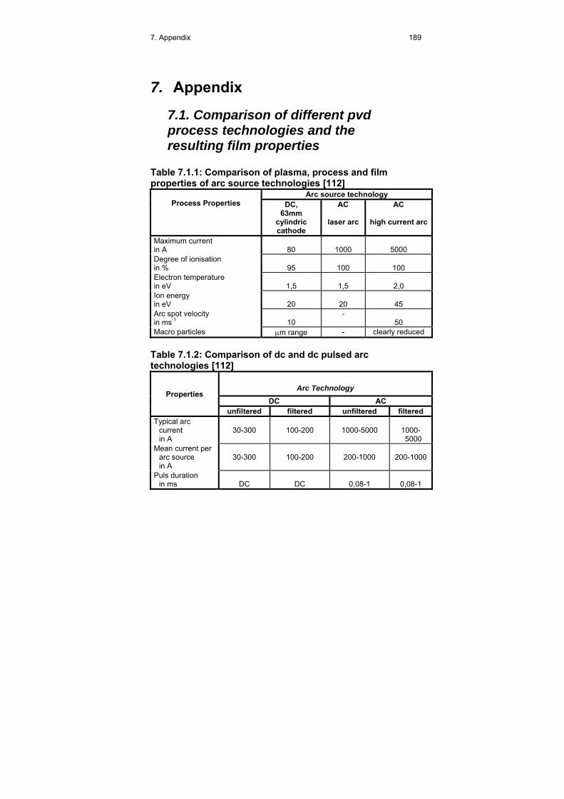
7. Appendix 189
7. Appendix
7.1. Comparison of different pvd process technologies and the resulting film properties
Table 7.1.1: Comparison of plasma, process and film properties of arc source technologies [112]
Arc source technology Process Properties DC,
63mm cylindric cathode
AC
laser arc
AC
high current arc
Maximum current in A
80
1000
5000
Degree of ionisation in %
95
100
100
Electron temperature in eV
1,5
1,5
2,0
Ion energy in eV
20
20
45
Arc spot velocity in ms-1
10
- 50
Macro particles μm range - clearly reduced Table 7.1.2: Comparison of dc and dc pulsed arc technologies [112]
Arc Technology DC AC
Properties
unfiltered filtered unfiltered filtered Typical arc
current in A
30-300
100-200
1000-5000
1000-5000
Mean current per arc source in A
30-300
100-200
200-1000
200-1000
Puls duration in ms
DC
DC
0,08-1
0,08-1

190 7. Appendix
Arc Technologie DC AC
Properties
unfiltered filtered unfiltered filtered Max. deposition
rate in μmh-1
<20
<10
800
200
Typical film
systems
AlTiN, TiN,
CrN, ZrN, TiCN
DLC, metals, hard coatings
DLC
DLC, copper, oxides
Applications
tools,
components, decorative
films
tools,
components, electronics,
tools,
components, laser mirrors
hard disc, interface
layers
Table 7.1.3: Properties of different hard coatings produced by different PVD processes
Coating material
Microhardness GPa
Friction coefficient
Special process and coating properties
Process: Arc Source Evaporation [45, 71]
TiN 25-30 0.4 TS=600°C, CC=gold-yellow
TiAlN 32 0.25 TS=900°C, CC=violet-grey
TiCN 29 0.4 TS=400°C, CC=blue-grey
AlCrN 31 0.35 TS=1100°C, CC=blue-grey
CrC 21 0.5 TS=700°C, CC=silver-grey
CrN 17-21 0.5 TS=700°C, CC=silver-grey
WC/C 15 0.1 - 0.2 TS=300°C, CC=anthracite
TS … max. service temperature, CC … coating colour

7. Appendix 191
Coating material
Microhardness GPa
Friction coefficient
Special process and coating properties
Process: CFUBM – Closed Field Unbalanced Magnetron Sputtering [84]
TiAlCrN 25 0,68 TD=450°C, UBias=-75V
CrN 21 0,49 TD=250°C, UBias=-100V
TiAlN–CrN 32 0,56 TD=450°C, UBias=-75V TiAlN–VN 35 0,40 TD=450°C, UBias=-75V CrN–NbN 35 0,63 TD=450°C, UBias=-75V TD … deposition temperature, UBias … substrate bias voltage,
Process: Combined Cathodic Arc/Unbalanced Magnetron Sputtering [105]
cBN 60-65 on silicon 0,4 FC=20N, cBN 55-60 on steel 0,4 FC=25N, TiN 25-30 0,7 FC=30-50N, DLC 25-33 0,2 FC=29N, Diamond 80-100 >0,2 --- FC … critical load in scratch test
7.2. Comparison of the optical and mechanical properties
Influence of the PVD process and its parameters on the density and the refractive index: Density and refractive index of isotropic materials are interrelated by the Lorentz-Lorenz equation. The mean refractive index can be calculated for the general case from:
molfmol
molmolff RM
MRn
ρ
ρ
−
+=
22 7.2.1
if the mean film density ρf is known, Rmol is the molar refraction, which can be calculated from single crystal data, and Mmol is the molar weight. If we use the packing density p, which is defined as the ratio of the average film density ρf and the bulk density ρm, the correlation between the packing density p and the refractive index n is given by:

192 7. Appendix
12
2
12
2
2
2
−
+
+
−==
m
m
f
f
m
f
nn
n
np
ρρ
7.2.2
A linear dependence between the refractive index n and film density ρf can be observed for evaporated, ion- and plasma-assisted films. Table 6.2.1: Refractive indices at 550nm of different metal oxides deposited by different ion plating techniques and compared with conventional evaporation [96]
Coating material Process SiO2 Ta2O5 TiO2 Al2O5 ZrO2
RE TS=300°C
1,46
2,10
2,34-2,44 1,61 1,96
RAPSIP TS=50°C
1,47
2,12
2,38
1,63 2,10
RLVIP TS=50-80°C
1,48
2,24
2,48-2,55 1,66 2,18
TS … Substrate temperature RE … Reactive Evaporation, RAPSIP … Reactive Advanced Plasma Source Ion Plating, RLVIP … Reactive Low Voltage Ion Plating
Influence of process parameters on the mechanical film stress A strong correlation exists between the intrinsic stress and the film density. In general, evaporated films have low density, open columnar microstructure and tensile intrinsic stress, while sputter deposited or ion plated films have higher density, close-packed microstructure and compressive stress. It is further known, that evaporated films prepared under continuous bombardment with ions of increasing kinetic energy are densified and show stress changes from tensile to compressive [97]. One problem in highly stressed films is mechanical failures like cracking or delamination of the films. Tensile stresses cause cracks in the film perpendicular to the film plane and delamination is typical for compressive stress.

7. Appendix 193
Responsible for these film failures is not the film stress for itself but the elastic energy Eelast stored in the film. Assuming that the film stress can be considered to be biaxial and isotropic in the film plane and independent on film thickness tf , the elastic energy Eelast per unit surface stored in the film is [98]:
( )felast t
EE νσ −
=12 7.2.3
The mechanical stability of the film-substrate system becomes critical when the stored elastic energy approaches and exceeds a critical value Ecrit, which is determined by a critical stress value σcrit, and the Griffith criterion [99] with the crack length h, omitting ν and surface energy γ.
2
2 2 2σ
γγσ Et
Eh
E critcrit
crit ≅⇒≅≅ 7.2.4
This demonstrates that the two new surfaces formed by a crack contribute to the total surface energy with an increase of 2γ. When σ is constant and independent of film thickness t there exists a critical film thickness tcrit at which Eelast exceeds Ecrit and film fracture will occur when t>tcrit. In the case of delamination the Barenblatt model [100] is more appropriate. Similar to 5.7.4 obtaining a critical energy for delamination leads to a critical stress value and finally to a critical film thickness:
2σγ E
t dcrit ≅ 7.2.5
where the surface energy is given by
γd = γs + γf + γi, 7.2.6
s … substrate, f … film, i … stands for the part where substrate and film were never joined

194 7. Appendix
The investigations show that, by the use of fracture theory, the criterion for film-substrate mechanical stability is dependent on γ, γd, σ and t and that the equations that describe the criteria for fracture and delamination have in principle the same form. To avoid catastrophic film failure, σ2t must be reduced in some manner. Varying the deposition parameters or changing the process technology can reduce the film stress. Evaporation, sputtering and energetic ion and coating material deposition processes operated with different sets of parameters cause different structures and microstructures so that the films of the same material but produced by different technologies generally also have different stress values. Hence, the possibility exists of influencing stresses in a desired way. In films deposited via vacuum evaporation, in the absence of any external agency (including contamination), tensile stresses are normally observed. Impurities in the deposition atmosphere of films deposited by evaporation cause the stresses to become compressive. Several mechanisms are probably involved in this phenomenon. Theoretical treatments often explain the origin of compressive stress as a consequence of energetic particle bombardment. Peening processes cause atoms to become incorporated into the growing .lm with a number quite higher than would be obtained otherwise since sufficient energetic atoms may be forced into spaces too small to accommodate them under thermal equilibrium conditions. Generally, vacuum deposited films and sputter deposited films prepared at high gas pressures have tensile stresses which may be anisotropic with off-normal angle of incidence deposition. In low-pressure sputter deposition and ion plating, energetic particle bombardment gives rise to high compressive stresses due to the recoil implantations of surface atoms [101, 102, 103]. Studies of deposited films with concurrent bombardment have shown that the conversion of tensile to compressive stress is very dependent on the ratio of bombarding species to depositing species [97]. In plasma processing the residual .lm stress may be very sensitive to the substrate bias and gas pressure during deposition in a plasma

7. Appendix 195
environment [104, 105]. The lattice strain associated with the film stress represents stored energy and this energy along with a high concentration of lattice defects leads to a lowering of the recrystallisation temperature in crystalline materials, a lowered strain point in glassy materials, a high chemical etch rate, electro migration problems, void growth in metallization lines by creep or other such mass transport effects. Film property modifications by ion bombardment are mainly caused by momentum transfer from the ions to the .lm atoms. Experiments on a reactive low voltage ion plating (RLVIP) process with dielectrics showed that reactive film deposition in presence of excited and ionised atoms and molecules of higher energy leads to the formation of dense chemical compound films. The high density of such films is responsible for the relatively high refractive index and the compressive stress. Ion bombardment induced local chemical defects may increase the extinction coefficient value when high ion current densities and ion energies of several tens of eV are applied in film production. Film deposition with low ion current densities and low ion energies produce stoichiometric coatings with very low extinction coefficient, low density, low stress and low refractive index. The optical and mechanical stability of such films is, however, often insufficient in such cases. The films need to be densified by a longer lasting post-deposition heat treatment at temperature higher than 300°C. This leads to a decrease in physical thickness and an increase in the refractive index and environmental stability. Heat treatment of dense films often causes microstructural relaxation phenomena and oxidation resulting in a decrease of the .lm density, extinction coefficient and intrinsic stress, there the physical film thickness if increased [106, 107]. As the total gas pressure of the vacuum atmosphere rises, the mean free path length in PVD processes is reduced. The paths by which neutrals, non-decelerated particles can travel or along which ionised particles can be accelerated by electrical fields are shortened. The kinetic energy of the particles impinging on the growing .lm decreases, which causes a decrease in growth-induced compressive stresses with rising total pressure. If the coating is deposited without

196 7. Appendix
applying a bias voltage, tensile stresses may even occur in the film. If the reactive gas component of the vacuum atmosphere is increased at constant total gas pressure, the number of dissociated and ionised gas particles, which can be accelerated on to the substrate, be incorporated in the coating and contribute to the formation of the lattice, rises. As the reactive gas component increases, the propagation of reactive gas atoms in the coating will therefore also rise until certain saturation points are reached. At higher reactive gas pressures, higher compressive stresses then occur.
Table 7.2.2: Stress values of SiO2 deposited with different technologies
Process Stress in MPa Reference RFMS – radio frequency magnetron sputtering
-150 to –270 -150 to –200
[177]
DCMS – direct current magnetron sputtering
-150 to –250 [177]
RAPSIP - reactive advanced plasma source ion plating
-100 to -500 [178]
RE - reactive evaporation -100 to -500 [179] PECVD – plasma enhanced chemical vapour deposition
-70 to –80 [180] [181]
RIP – reactive ion plating up to –1000 [182] RLVIP – reactive low voltage ion plating -500 to –1000 [183] IBAD – ion beam assisted deposition -10 to -470
-610 to -1900 [184] [185]
Compressive stress: negative sign, tensile stress: positive sign
Table 7.2.3: Stress values of TiO2 deposited with different technologies
Process Stress in MPa References RAPSIP - reactive advanced plasma source ion plating
110 to 190 95
[186], [178]
RE - reactive evaporation 165 to 300 220 to 300
[186], [187], [188]
MFMS – mid frequency magnetron sputtering
-500 to -900 [187]
SC – spin coating 100 to 250 [187], [188] PICVD – plasma impulse chemical vapour deposition
0 to 400 [187]
RIP – reactive ion plating -150 to -400 [187], [182],

7. Appendix 197
[188] RLVIP – reactive low voltage ion plating -800 [189] IBAD – ion beam assisted deposition -540 [185] FAD – filtered arc deposition -700 to -2500 [190] Compressive stress: negative sign, tensile stress: positive sign
Table 7.2.4: Stress values of Al2O3 deposited with different technologies
Process Stress in MPa References RFMS – radio frequency magnetron sputtering
-250 to –1200 -200 to -300
[191] [192]
RE - reactive evaporation +100 [193] RIP – reactive ion plating -210 [182] Compressive stress: negative sign, tensile stress: positive sign
Table 7.2.5: Stress values of Ta2O5 deposited with different technologies
Process Stress in MPa References RFMS – radio frequency magnetron sputtering
-200 to -350 [194]
RIP – reactive ion plating -200 [182] RLVIP – reactive low voltage ion plating -400 to -1000 [183] Compressive stress: negative sign, tensile stress: positive sign
Table 7.2.6: Stress values of Nb2O5 deposited with different technologies
Process Stress in MPa References RFMS – radio frequency magnetron sputtering
+100 to -1100
DCMS – direct current magnetron sputtering
-100 to -250 [177]
RLVIP – reactive low voltage ion plating -200 to -500 [195] Compressive stress: negative sign, tensile stress: positive sign
198 7. Appendix
7.3. Some modern applications of plasma and ion assisted PVD process technologies
Hard coatings for tool applications: In the case of PVD techniques for hard coatings (e.g. for cutting tools), the most commonly used processes today are evaporation, sputtering and arc source deposition. Electron beam evaporation of titanium in a vacuum chamber and reaction with a nitrogen plasma to deposit TiN was the first successful application of PVD for cutting tools. Later on, deposition by sputtering from a solid target was used, and this technology has been considerably advanced during the last decade by several scientific groups and companies [119-125]. Today, many variations of sputtering and arc techniques are used commercially, whereby the arc technology is the most important technology to deposit coatings for cutting tools. The main advantages of the arc technology are the high degree of ionisation (with multiple ionised particles), the high kinetic energy of the particle and the high deposition rates. One drawback of the arc technology is that neutral clusters may evaporate from the arc sources, which leads to droplets (macroparticles) on the substrate surface. Reduction or prevention of macroparticles in arc deposition can be done for example by filtered arc technology, using electromagnetic filters to filter out the neutral macroparticles and clusters. Another method to reduce macroparticles is Nano Dispersed Arc Jet (NDAJ) technique, in which a special designed magnetic field enables the arc to cover the whole target surface at a higher speed. Therefore the average size of neutral particles is dramatically decreased – smoother coatings are achieved without loosing deposition rate [91]. Other promising deposition technology for hard coating applications are pulsed sputtering techniques (PMS) and high power pulsed magnetron sputtering (HIPIMS) [166, 127, 196-199]. Some important coating properties for tool applications are hardness and ductility, resistance against abrasive wear, coefficient of friction, oxidation resistance, chemically stability

7. Appendix 199
or thermophysical properties. In many cases not only the improvement of a single coating property (i.e. hardness) is sufficient enough to improve the properties and performance of coatings, only the improvement of a combination of coating properties leads to a better product [128]. Typical PVD hard coatings are titanium nitride (TiN), titanium carbonitride (TiCN), titanium aluminum nitride (Ti0,5,Al0,5N), zirconium nitride (ZrN), titanium zirconium nitride (TiZrN), chromium nitride (CrN), aluminum chromium nitride (AlCrN), tungsten carbide (WC) and diamond-like carbon (DLC). TiN is characterised by a broad application range, moderate hardness and good abrasive wear resistance. Substitution of nitrogen atoms by non metals like carbon yielded TiCN – a broad band coating with higher hardness and improved abrasive wear resistance. Introduction of aluminium in the cubic face centered TiN structure improved oxidation resistance of PVD coatings. Recently a new generation of coatings were introduced, based on the Al-Cr-N system. This system is characterised by superior abrasive wear resistance and improved oxidation resistance, which are the key properties required for example for gear cutting applications (see table 7.1.3). A new area in the field of hard coatings is the deposition of nano composite (nc) coatings, which show superior mechanical properties. Nano crystalline transition metal nitrides (using metals like Ti, Zr, W) are embedded in a amorphous or nano crystalline matrix of Si3N4, which leads to high hardness of the coatings. It was shown that also after a high temperature treatment (i.e. 1000°C) the high hardness does not decrease [122, 129, 130]. Other approaches in the field of tool applications are superhard coatings and superlattice coatings. Superhard coating means a coating whose Vickers hardness exceeds 40GPa. These coatings can be divided into intrinsic, such as diamond, c-BN and some ternary compounds from the B-N-C triangle [131, 132], and extrinsic, whose mechanical properties are determined by their microstructure [133]. Diamond and cubic boron nitride (c-BN) are some prominent example for intrinsic super hard coatings [134] and an example for extrinsic superhard coatings are superlattices coatings [135].

200 7. Appendix
Superlattice coatings are based on the idea of sequential deposition of ultra-thin layers of two compounds with a close match of lattice parameters, such that they can develop coherent interfaces leading to a superlattice structure. The most promising coatings have been done with refractory metal nitrides, like WC-TiN, TiN/NbN, TiN/AlN, and TiN/VN. These coatings are typically deposited by reactive magnetron sputtering, and have demonstrated significant improvements in hardness and wear resistance as compared to TiN and other conventional hard coatings. The largest enhancement of the hardness of such superlattice coatings is found for an optimum modulation period of 5-10nm followed by its decrease for smaller periods due to interdiffusion and mixing at the interface [136-142]. Large Area Glass Coating: Over the last decade, modern magnetron sputtering technologies, like pulsed plasma sputtering and dual magnetron sputtering, has become one of the most important methods for depositing thin films on large areas [143-145]. As a result of the high plasma density, uniform plasma distribution in the longitudinal direction and high deposition rate magnetron sputtering is the leading process for large area coating. Some of the key features are: relative ease for up-scaling, high mass productivity (high deposition rate), good control of layer thickness, uniformity and quality, combined with a wide variety of available sputter materials. The main applications for large area glass PVD coatings can be found in the architectural, automotive and display industry. Typically applications in the field of large area deposition are low emissivity and solar control coatings, anti-reflection (AR) and anti-reflection anti-static (ARAS) coatings, indium tin oxide coatings (ITO) for flat displays, electrochromic coatings for smart windows or functional coatings for solar cells. Pulsed magnetron sputtering, at frequencies in the 50 kHz range, solve the disappearing anode problem and provide stable operating conditions with very low arcing. The quality of the deposited films is very high and the films show higher density, a smoother surface, an increased hardness and

7. Appendix 201
improved optical properties compared with films deposited by dc sputtering [146, 147. Table 7.3.1: Deposition rates for different compound layers [144]
Dynamic deposition rate in nm at a substrate speed
of 1m/min
Material
DC single magnetron
MF double magnetron
SiO2 5-10 70 Si3N4 20 40 SnO2 40 80 TiO2 5-10 40
Modern in-line coaters for architectural glass coatings enable a high throughput with glass substrates with dimensions up to 3x6 meters. Such a system is 4m in width and up to 150m in length and it consists of an entrance and an exit chamber, two buffer chambers and a sputter chamber with different sputter modules and two transfer chambers [144]. Focusing on large area cathodic arc deposition, it has to be mentioned that the arc plasma is produced at cathode spots, that means, the plasma comes from point sources and therefore must be expanded and distributed to be suitable for large area coating. Traditionally, large area arc coating is done using either an array of cathodic arc sources or using large planar or cylindrical cathodes in conjunction with magnetic or electric arc cathode spot steering (steered arc) [148-150]. Recent developments addressing the particle issue in large area coatings by introducing dual filter arrangements for batch coating [151] and linear filters with rectangular cross section for in-line coating systems [152, 153] Flat panel displays: A fast-growing market which is strongly dependent on plasma and PVD technology is driven by flat panel displays used in office automation, vehicles and television sets. Flat panel displays require a lot of different thin film systems like ITO, SiO2 barrier layers, metal interconnects, black chromium,

202 7. Appendix
silicon nitride or α-silicon [154]. The main deposition technology used for flat panel display application is rf and pulsed magnetron sputtering, where special designed cathodes provide high target utilization and effective arc suppression leads to fewer defects and good uniformity. The most important display properties, like luminance (cd/m2), colour performance (RGB), resolution (size and total number of pixels), display speed or contrast, are directly linked to the properties of the human eye and therefore the properties of displays should meet certain standard values in order for the eye to see proper images[155]. Table 7.3.2: Main flat panel technologies [155]
Electronic displays – Flat panles
Direct view
Projection
LCD Liquid crystal displays
LCD’s or Liquid crystal light valves
EL Electroluminescent displays
DMD – Digital micromirror displays
PDP Plasma display panels
GLV – Grating light valves
FED Field emission displays
Laser projectors
A common problem for all displays is that their images may be degraded or completely disappear when they are viewed under strong ambient illumination. AR (antireflection) coatings are most commonly used for enhancing the display contrast, by increasing the total amount of images light of the display. The principle relationship: 1=T+R+A (T-transmission, R-reflection, A-absorption) shows that a reduction in R will lead to an increase in T, if A is not changed. An antireflection systems deposited by PVD techniques normally consists of several layers [156, 157]. Also black layer coatings, based on thin film interference, are used to remove unwanted reflected ambient light [158, 159]. Colour filters are essential components for non-emissive flat panel application, because it is necessary to generate three primary colour images from which the full colour image can be

7. Appendix 203
formed. To minimise any light loss, time sequential or simultaneous colour schemes, like dichroic filters, are often used. Dichroic filters consists of multilayer structure of low- and high refractive index coatings materials like TiO2, Ta2O5, Nb2O5, SiO2, Al2O3 and ZrO2 [155, 160]. Energetic PVD processes like ion-assisted deposition, plasma assisted ion plating and rf or dc pulsed magnetron sputtering are often used to deposit such filter systems. Dichroic filters transmit or reflect R, G and B light and the performance of these filters is characterised by the position and the sharpness of the cut-off edges and by the transmission or reflection in the pass- or stop-bands at certain angles of incidence. In projection displays they can separate for example white light into RGB colour light or combine RGB colour images or they can perform both of functions [161-163]. Another component required for flat panels (LCD’s) applications are polarizers and polarizing beam-splitters (PBS), which generate polarized light from the un-polarized light sources. The main properties of polarizers are the working wavelength range, the transmittance or reflectance of the desired polarization, the angular field and the extinction ratio. In case of PBS these properties must be fulfilled for both the reflected and the transmitted light. Most often used polarizers and PBS in display applications are polariod polarizers, Metal Wire Grid Polarizers, Birefringent Multilayer Polarizers, MacNeille Polarizers and LiLi-PBS [155, 163-165]. Flat displays and specially projectors are quite complicated optical systems with a lot of different coating components. In a typical LCD projector for example a lot of different optical coatings, produced by modern PVD techniques, are in use. Cold and hot mirrors, deposited as dielectric multilayer coatings, are used to remove UV and IR radiation from arc lamps. Aluminum mirrors are used to redirect the light beams, and colour-balancing coatings sometimes are needed to correct the balance of the RGB colours in the display [155].

204 7. Appendix
7.4. Ionisation potentials of atoms and molecules (in eV)
As can be seen in the table, the ionisation potentials span the range from 8 to 25eV, which are well above the mean electron energy in a cold plasma. Thus, only electrons in the high-energy tail of the electron distribution can contribute to the ionisation reactions.
neutral ion ionisation potentials Al Al+ 6; 18,8; 28,4 Ar Ar+ 15,8; 27,6; 40,9 F F+ 17,4; 35,0 Cl Cl+ 13; 23,8; 39,9 H H+ 13,6 He He+ 24,6; 54,4 N N+ 14,5; 29,6; 47,4 O O+ 13,6; 35,2; 54,9 Si Si+ 8,1; 16,3 Ti Ti+ 6,8;13,6; 27,1 CH4 CH4+ 13 C2H2 C2H2+ 11,4 H2 H2+ 15,4 HF HF+ 17 H2O H2O+ 12,6 N2 N2+ 15,6 O2 O2+ 12,2 SiH4 SiH4+ 12,2

7. Appendix 205
7.5. Units CGS-units:
Erg: 1 erg = 10-7 J Dyne: 1 dyn = 10-5 N Poise: 1 P = 1 dyn s/cm2 = 0.1 Pa s Stokes: 1 St = 1 cm2/s = 10-4 m2/s Gauss: 1 G = 10-4 T Oersted: 1 Oe = (1000/(4 pi)) A/m Maxwell: 1 Mx = 10-8 Wb Stilb: 1 sb = 1 cd/cm2 = 104 cd/m2 Phot: 1 ph = 104 lx
SI-units:
Length: meter [m] Mass: kilogram [kg] Time: second [s] Electric current: ampere [A] Temperature: kelvin [K] Amount of substance: mole [mol] Luminous intensity: candela [cd]

206 7. Appendix
7.6. Periodic table of elements

7. Appendix 207
7.7. Table of isotopes of elements
nb element symbol amu rel. amount [%]
1 hydrogen H 1 99,985 D 2 0,01492 2 helium He 3 0,000137 4 99,999863 3 lithium Li 6 7,42 7 92,58 4 beryllium Be 9 100 5 boron B 10 19,61 11 80,39 6 carbon C 12 98,893 13 1,107 7 nitrogen N 14 99,6337 15 0,3663 8 oxygen O 16 99,759 17 0,0374 18 0,2039 9 fluorine F 19 100 10 neon Ne 20 90,92 21 0,26 22 8,82 11 sodium Na 23 100 12 magnesium Mg 24 78,70 25 10,13 26 11,17 13 aluminium Al 27 100 14 silicon Si 28 92,21 29 4,70 30 3,09 15 phosphorus P 31 100 16 sulfur S 32 95,0 33 0,76 34 4,22

208 7. Appendix
nb element symbol amu rel. amount [%]
17 chlorine Cl 35 75,53 37 24,47 18 argon Ar 36 0,337 38 0,063 40 99,600 19 potassium K 39 93,1 40 0,0118 41 6,88 20 calcium Ca 40 96,97 42 0,64 43 0,15 44 2,06 46 0,003 48 0,18 21 scandium Sc 45 100 22 titan Ti 46 7,93 47 7,28 48 73,94 49 5,51 50 5,34 23 vanadium V 50 0,24 52 99,76 24 chromium Cr 50 4,31 52 83,76 53 9,55 54 2,38 25 manganese Mn 55 100 26 iron Fe 54 5,82 56 91,66 57 2,19 58 0,33 27 cobalt Co 59 100

7. Appendix 209
nb element symbol amu rel. amount
[%] 28 nickel Ni 58 67,88 60 26,23 61 1,19 62 3,66 64 1,08 29 copper Cu 63 69,09 65 30,91 30 zinc Zn 64 48,89 66 27,81 67 4,11 68 18,57 70 0,62 31 gallium Ga 69 60,4 70 39,6 32 germanium Ge 70 20,52 72 27,43 73 7,76 74 36,64 76 7,76 33 arsenic As 75 100 34 selenium Se 74 0,87 76 9,02 77 7,58 78 23,52 80 49,82 82 9,19 35 bromine Br 79 50,54 81 49,46 36 krypton Kr 78 0,35 80 2,27 82 11,56 83 11,55 84 56,90 86 17,37
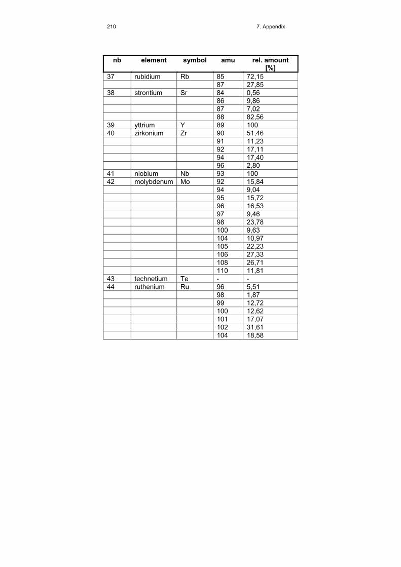
210 7. Appendix
nb element symbol amu rel. amount
[%] 37 rubidium Rb 85 72,15 87 27,85 38 strontium Sr 84 0,56 86 9,86 87 7,02 88 82,56 39 yttrium Y 89 100 40 zirkonium Zr 90 51,46 91 11,23 92 17,11 94 17,40 96 2,80 41 niobium Nb 93 100 42 molybdenum Mo 92 15,84 94 9,04 95 15,72 96 16,53 97 9,46 98 23,78 100 9,63 104 10,97 105 22,23 106 27,33 108 26,71 110 11,81 43 technetium Te - - 44 ruthenium Ru 96 5,51 98 1,87 99 12,72 100 12,62 101 17,07 102 31,61 104 18,58

7. Appendix 211
nb element symbol amu rel. amount
[%] 45 rhodium Rh 103 100 46 palladium Pd 102 0,96 47 silber Ag 107 51,35 109 48,65 48 cadmium Cd 106 1,22 108 0,875 110 12,39 111 12,75 112 24,07 113 12,26 114 28,86 116 7,58 49 indium In 113 4,28 115 95,72 50 tin Sn 112 0,96 114 0,66 115 0,35 116 14,30 117 7,61 118 24,03 119 8,58 120 32,85 122 4,72 124 5,94 51 antimony Sb 121 57,25 123 42,75 52 tellurium Te 120 0,09 122 2,46 123 0,87 124 4,61 125 6,99 126 18,71 128 31,79 130 34,48
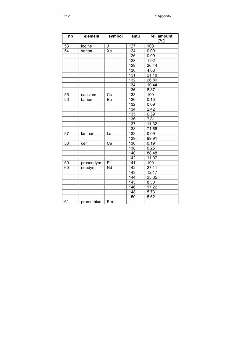
212 7. Appendix
nb element symbol amu rel. amount
[%] 53 iodine J 127 100 54 xenon Xe 124 0,09 126 0,09 128 1,92 129 26,44 130 4,08 131 21,18 132 26,89 134 10,44 136 8,87 55 caesium Cs 133 100 56 barium Ba 130 0,10 132 0,09 134 2,42 135 6,59 136 7,81 137 11,32 138 71,66 57 lanthan La 138 0,09 139 99,91 58 cer Ce 136 0,19 138 0,25 140 88,48 142 11,07 59 praseodym Pr 141 100 60 neodym Nd 142 27,11 143 12,17 144 23,85 145 8,30 146 17,22 148 5,73 150 5,62 61 promethium Pm - -

7. Appendix 213
nb element symbol amu rel. amount
[%] 62 samarium Sm 144 3,09 147 14,97 148 11,24 149 13,83 150 7,44 152 26,72 154 22,71 63 europium Eu 151 47,82 153 52,18 64 gadolinium Gd 152 0,20 154 2,15 155 14,73 156 20,47 157 15,68 158 24,87 160 21,90 65 terbium Tb 159 100 66 dysprosium Dy 156 0,05 158 0,09 160 2,29 161 18,88 162 25,53 163 24,97 164 28,18 67 holmium Ho 165 100 68 erbium Er 162 0,14 164 1,56 166 33,41 167 22,94 168 27,07 170 14,88 69 thulium Tm 169 100

214 7. Appendix
nb element symbol amu rel. amount
[%] 70 ytterbium Yb 168 0,14 170 3,03 171 14,31 172 21,82 173 16,13 174 31,84 176 12,73 71 lutetium Lu 175 97,41 176 2,59 72 hafnium Hf 174 0,18 176 5,20 177 18,50 178 27,14 179 13,75 180 35,24 73 tantalium Ta 180 0,01 181 99,99 74 tungsten W 180 0,13 182 26,41 183 14,40 184 30,64 186 28,41 75 rhenium Re 185 37,07 187 62,93 76 osmium Os 184 0,02 186 1,59 187 1,64 188 13,3 189 16,1 190 26,4 192 41,0 77 iridium Ir 191 37,3 193 62,7

7. Appendix 215
nb element symbol amu rel. amount
[%] 78 platinium Pt 190 0,01 192 0,78 194 32,9 195 33,8 196 25,3 198 7,21 79 gold Au 197 100 80 mercury Hg 196 0,15 198 10,02 199 16,84 200 23,13 201 13,22 202 29,80 204 6,85 81 thallium Tl 203 29,50 205 70,50

216 8. Publications
8. Publications Cooperation in the following scientific projects:
2005-2007: PM-Tech4 SOFC: Development and validation of power metallurgical materials and production methods for the application in high temperature fuel cells
2005-2007: HiPlas: High Density Plasma Sources GZ: BMWA-97.210/0004-C1/9/2005
2005-2007: NEWTRESI - New Treatment for Surgical Implants, CRAFT: C00P–CT-2004–508344
2004-2006: Set up of a mobile coating chamber Ticnet project: MoCoat
2004-2006: Functional coatings for tools Ticnet project: ToolCoat
2002-2005: Analysing, modelling and upscaling of different pvd TiC processes for medical implant applications EU-Projekt: IGOID
2000-2002: Plasma characterisation of APS (advanced plasma source) from Leybold Industrial project in cooperation with Fraunhofer Institute for Applied Optics Jena
1997-2001: Investigations on the plasma of ion and plasma assisted pvd processes EU Brite Euram project: TIPCOAT
1997: Herstellung verlustarmer optischer Schichten, FWF project P11515ÖPY
Contributions to scientific books:
Review Book Thin Solid Films, 2008 G.N. Strauss, S. Schlichtherle, Chapter: Modern plasma and ion assisted pvd process technologies
Jahrbuch Oberflächentechnik, Leuze Verlag, 2005 G.N. Strauss, S. Schlichtherle, Chapter: Arc-Source Beschichtungsverfahren
Jahrbuch Oberflächentechnik, Leuze Verlag, 2004 G.N. Strauss, S. Schlichtherle, Chapter: Plasma analysis of different pvd processes

8. Publications 217
Optical Interference Coatings, Springer Verlag, 2003 G.N. Strauss, Chapter: Mechanical stress in optical coatings
Publications in Scientific Journals:
1) G.N. Strauss, S. Schlichtherle, H.K. Pulker, Plasma Inverstigations of PVD processes operating in dc continuous and/or dc pulsed mode, Vakuum in Forschung und Praxis, Vol.19-4, (2007)
2) Hallbauer, D. Huber, G.N. Strauss, S. Schlichtherle, A. Kunz, H.K. Pulker, Overview about the optical properties abd mechanical stress of different dielectric thin films produced by reactive low voltage ion plating, Thin Solid Films, (2007)
3) Schintlmeister, S. Schlichtherle, G. Strauss, P. Wilhartitz; Properties of High Quality Optical Nb2O5 Thin Films deposited by Plasma Monitored DC and DC - Pulsed Reactive Magnetron Sputtering of metallic Niobium and Ceramic Niobium Oxide Sputtering Targets. Proceedings of SVC, (2005)
4) G.N. Strauss, H.K. Pulker, M. Meyer, P. Hatto, C. Davis, H. Jehn, M. Balzer, C. Misiano, V. Silipo, E. Olzi, R. Molena, F. Passaretti; Low-Vacuum Low-Cost Deposition of Tribological Coatings. Vakuum in Forschung und Praxis, Vol. 15, No. 3, 134-138, (2003)
5) G.N. Strauss, H.K. Pulker; Plasma diagnostic of ion and plasma PVD processes. Thin Solid Films, Volume 442, Issues 1-2, Pages 66-73, (2003)
6) G.N. Strauss, Mechanical stress in optical coatings, Optical Interference Coatings, Springer Verlag, (2003)
7) G.N. Strauss, H.K. Pulker, Plasma diagnostic of ion and plasma pvd processes, Proceedings of 4th ICCG, (2002)
8) G.N. Strauss, et.al,, Plasma Analysis of Different TiN PVD Processes at Various Process Parameters, Galvanotechnik, Bd.93, Heft 6, (2002), 1576-1579
9) G.N. Strauss, Charakterisierung des Plasmas in ionen- und plasmaunterstützen PVD-Prozessen, Galvanotechnik, Bd.91, Heft 9, (2000), 2586-2592

218 8. Publications
10) G.N. Strauss, Untersucung des Plasmas für das reaktive Niedervolt-Ionenplattieren, H.K. Pulker, Vakuum in Forschung und Praxis (2000), Nr.1, 25-28
11) G.N. Strauss, W. Lechner, Gas pressure influence an optical and mechanical properties of Ta2O5 films produced by reactive low voltage ion plating (RLVIP), H.K. Pulker, Thin Solid Films, 351 (1999), 53-56
12) W. Lechner, G.N. Strauss, Correlation between optical and mechanical properties of ion plated Ta2O5 films, H.K. Pulker, SVC-41st Annual Technical Conference Proccedings, 1998, 287-290
13) G.N. Strauss, Q.D. Nguyen, H.K. Pulker, Mechanical stress in thin SiO2 and Ta2O5 films produced by reactive low voltage ion plating (RLVIP), Journal of Non-Crystalline Solids, 218 (1997), 256-261
Contribution to conferences:
G.N. Strauss, S. Schlichtherle, Modern Plasma and Ion Assisted PVD Process Technology, Interacademica 2007, Hamamatsu, Japan, 2007
G. Kunschert, K. H. Kailer, S. Schlichtherle, G. N. Strauss, Ceramic PVD Coatings as Dense/Thin Barrier Layers on Interconnect Components for SOFC Application, 2007
G.N. Strauss, S. Schlichtherle, H.K. Pulker, Plasma investigation of dc and dc pulsed sputtering processes, 12. NdVak, Dresden, 2004
G.N. Strauss, Plasma Diagnostic of various Ion and Plasma PVD Processes, 8th Conference on Plasma Surface Engineering, Sept. 9.-13-2002, Garmisch-Partenkirchen, Germany, 2002
G.N. Strauss, S. Schlichtherle, H.K. Pulker, Sondenmesstechnik zur Charakterisierung von reaktiven Ionenplattier-Prozessen, 9.Neues Dresdner Vakuumtechnisches Kolloquium, 18. und 19.10.2001, Dresden, Germany, 2001
G.N. Strauss, H.K. Pulker, Sondenmesstechnik zur Charakterisierung von reaktiven Ionenplattier-Prozessen, 8.Neues Dresdner Vakuumtechnisches

8. Publications 219
Kolloquium, 20. und 21.10.2000, Dresden, Germany, 2000
G.N. Strauss, H.K. Pulker, Correlation between plasma properties and film properties in an Ion Plating Process (RLVIP), 4th Symbosium of European Vacuum Coaters, 25th Sept. - 27th Sept. 2000, Anzio (Rome) Italy
G.N. Strauss, H. Tafelmeier, Special features of tools used for substrate covering in Ion Plating Processes, 4th Symbosium of European Vacuum Coaters, 25th Sept. - 27th Sept. 2000, Anzio (Rome) Italy
G.N. Strauss, H.K. Pulker, Local coating testing chamber: On energy distribution in ion plating processes, 4th Symbosium of European Vacuum Coaters, 25th Sept. - 27th Sept. 2000, Anzio (Rome) Italy
G.N. Strauss, H.K. Pulker, Untersuchungen des Plasmas für das Reaktive Niederspannungs-Ionenplattieren, 7. Neues Dresdner Vakuumtechnisches Kolloquium, 14. und 15. Oktober 1999, Dresden, Germany, 1999
G.N. Strauss, W. Lechner, Correlation between Optical and Mechanical Properties of Ion Plating Ta2O5 films, 12th Symbosium on Application of Plasma Processes, 9th-13th February 1999, Liptovsky Jan, Slovakia
G.N. Strauss, W. Lechner, Gas Pressure Influence on the Optical and Mechanical Properties of Ta2O5 films produced by Reactive Ion Plating (RLVIP), 2nd
Symbosium of European Vacuum Coaters, 28th-30th September 1998, Anzio (Rome), Italy
G.N. Strauss, W. Lechner, Correlation between Optical and Mechanical Properties of Ion Plating Ta2O5 films, SVC – 41st Annual Technical Conference, 18th-23th April 1998, Boston (MA), USA
G.N. Strauss, Intrinsic Mechanical Stress in SiO2 and Ta2O5 films produced by Ion Plating, International Conference on Coatings on Glass, ICCG, 27th-31st October 1996, Saarbrücken, Germany

220 8. Publications
G.N. Strauss, Intrinsic Stress in SiO2 and Ta2O5 films produced by Ion Plating, Workshop of European Vacuum Coaters, 30th Sept. to 2nd October 1996, Anzio (Rome), Italy
Seminar talks, Georg N. Strauss:
• Interacademica 2007, Modern Plasma and Ion Assisted PVD Process Technologies, Hamamatsu, Japan
• BAP-Meeting 2006, Untersuchungen des Plasmas für das reaktive Niedervolt-Ionenplattieren, Innsbruck, Austria
• TFT Seminar 2005, Brennstoffzellen: Grundlagen, Varianten, Anwendungen, Seminar am Inst. für Ionenphysik, Universität Innsbruck, Austria
• TFT Seminar 2005, Sputtern: Grundlagen, Prozesse, Anwendungen, Seminar am Inst. für Ionenphysik, Universität Innsbruck, Austria
• OTTI Kolleg: 2002-2005: Herstellung dünner Schichten, Ionenplattieren und Wartung und Reinigung von Vakuum-Beschichtungsanlagen, Regensburg und Würzburg, Germany
• Advanced Materials 2003: Herstellung, Eigenschaften, Charakterisierung und Anwendung dünner Schichten, Ringvorlesung an der Universität Innsbruck, Innsbruck, Austria
• TFT Seminar 2003, Plasma analysis of different pvd process technologies, Seminar am Inst. für Ionenphysik, Universität Innsbruck, Austria
• TFT Seminar 2003, PVD process technology fort he deposition of TiC coating for medical implants, Seminar am Inst. für Ionenphysik, Universität Innsbruck, Austria
• IGOID Meeting 2001, Plasma diagnostic of PVD processes, Newcastle, England
• TFT Seminar 2001, Farday Cup Messungen am APS Beschichtungsprozess, Seminar am Inst. für Ionenphysik, Universität Innsbruck, Austria

8. Publications 221
• PAAPS Meeting 2001, Charakterisierung des APS Plasmas, IOF Jena, Fraunhofer Institut, Jena, Germany
• TIPCOAT Meeting 2001, Analysis of pulsed magnetron sputter source, Technical meeting TIPCOAT project, Bonassola, Italy
• Plasmaanalyse für APS Beschichtungsprozesse, IOF Jena, Fraunhofer Institut, 18.10.2000, Jena, Germany
• TFT Seminar 1999, Untersuchungen des Plasmas von reaktiven Ion Plating Prozessen, Seminar am Inst. für Ionenphysik, Universität Innsbruck, Austria
• Fraunhofer Seminar 1999, Mechanische Eigenschaften dünner dielektrischer Schichten, Fraunhofer Institut für Werkstoff- und Strahlentechnik, Dresden, Germany
• Fraunhofer Seminar 1998,Intrinsische Spannungen in dünnen dielektrischen Schichten, Seminar am Fraunhofer Institut für Angewandte Optik und Feinmechanik, Jena, Germany
• TFT Seminar 1996, Bestimmung des Elastizitätsmodul in dünnen Schichten, Seminar am Institut für Experimentalphysik, Innsbruck, Austria

222 9. References
9. References [1] H. K. Pulker, Coatings on Glass (sec.rev.edu.), Elsevier,
(1999) [2] Rointan F. Bunshah, Handbook of Deposition Technologies
for Films and Coatings, Noyes Publications, (1994) [3] D. M. Mattox, Handbook of Physical Vapor Deposition
(PVD) Processing, Noyes Publications, (1998) [4] S. M. Rossnagel, J. J. Cuomo, W. D. Westwood, Handbook
of Plasma Processing Technology, Noyes Publications, (1990)
[5] G. Janzen, Plasmatechnik, Hüthig Verlag, (1992) [6] A. Piel, Einführung in die Plasmaphysik, Vorlesungsskript ,
Christian-Albrechts-Universität Kiel, (1996) [7] J. A. Thornton, Diagnostic methods for sputtering plasmas,
J.Vac.Sci.Technol. 15(2), 188-192, 03/ 04, (1978) [8] A. Grill, Cold Plasmas in Material Fabrication, IBM
Research Division, IEEE Press, (1993) [9] Manory, Carmi, Avni, Grill, Thin Solid Films, 156: 79,
(1988) [10] S.C. Brown, opcit p.28 [11] S.C. Brown, opcit p.60 [12] C.M. Ferriera and J. Loureiro, J.Phys.D:Appl.Phys, 17:
1175, (1984) [13] J. Machet, P. Saulnier, J. Ezquerra and J. Gulle, ”Ion
Energy Distribution in Ion Plating” , Vacuum, 33:279 (1983)
[14] W. Lindinger, Pure Appl. Chem., 57:1223 (1985) [15] H.K. Pulker, ”Method of Producing Gold-Color Coatings” ,
US Patent # 4,254,159 (Mar 3, 1981) [16] H. Kaufman, ”Method of Depositing Hard Wear Resistant
Coatings on Substrates” , US Patent # 4,346,123 (Aug. 24, 1982)
[17] T.C. Tisone, ”Low Voltage Triode Sputtering with a Controlled Plasma” , Solid State Technol., 18(12):34 (1975)
[18] T.C. Tisone, P.D. Cruzan, ” Low Voltage Triode Sputtering” , J.Vac.Sci.Technol., 12(5):1058 (1975)
9. References 223
[19] S. Schiller, Goedicke K . Kircho¤ V. and Kopte T ., ”Pulsed Technology - A New Era of Magnetron Sputtering” , Proceedings of the 38th Annual Technical Conference, Society of Vacuum Coaters, p.239 (1995)
[20] J. Sellers, ”Asymmetric Bipolar Pulsed DC: The Enabling Technology for Reactive PVD” , Proceedings of the 39th Annual Technical Conference, Society of Vacuum Coaters, p.123 (1996)
[21] B. Windows and N. Savvides, ”Charged Particle Fluxes from Planar Magnetron Sputtering Sources” , J.Vac.Sci.Technol. A, 4(2):196 (1986)
[22] B. Windows and N. Savvides, ”Unbalanced DC Magnetrons as Sources of High Ion Fluxes” , J.Vac.Sci.Technol. A, 4(3) :453 (1986)
[23] B. Windows and N. Savvides, ”Unbalanced Magnetron Ion-Assisted Deposition and Property Modification of Thin Films” , J.Vac.Sci.Technol. A, 4(3):504 (1986)
[24] M.C. Vella, K.W. Ehler, D. Kippenhan, P.A. PincosyR.V. , Pyle, W.F. Di-Vergilio and V.V. Fosnight, ”Development of rf Plasma Generators for Neutral Beams” , J.Vac.Sci.Technol. A, 3:1218 (1985)
[25] J.W. Butterbaugh, L.D. Baston and H.H. Sawin, ”Measurement and Analysis of rf Glow Discharge Electrical Impedance and Network Power Loss” , J.Vac.Sci.Technol. A, 8(2) :916 (1990)
[26] C.M. Horwitz, ”Radio Frequency Sputtering - the Significance of Power Capacitively Coupled RF Discharges” , J.Appl.Phys., 58:4024 (1985)
[27] C.M. Horwitz, ”Radio Frequency Sheaths - Modeling and Experiments” , J.Vac.Sci.Technol. A, 8(4) :3123 (1990)
[28] C.M. Horwitz, ”Radio Frequency Sheaths - adjustable waveform model” , J.Vac.Sci.Technol. A, 8(4) :3132 (1990)
[29] W.D. Sproul, M.E. Graham, M.S. Wong, S. Lopez and D. Li, ”Reactive Direct Current Magentron Sputtering of Al Oxide Coatings” , J.Vac.Sci.Technol. A, 13(3):1188 (1995)
[30] R.L. Boxman, P.J. Martin and D.M. Sanders, Handbook of Vacuum Arc Science and Technology: Fundamentals and Applications, Noyes Publication (1995)

224 9. References
[31] D.M.Sanders, ”Review of Ion-based Coating Processes Derived from the Cathodic Arc” , J.Vac.Sci.Technol. A, 7(3) :2339 (1989)
[32] D.M.Sanders, D.M. Boercker and S. Falabella, ”Coating Technology Based on Vacuum Arc: A Review” , IEEE Trans. On Plasma Physics, 18(6):833, (1990)
[33] H. Ehrich, B. Hasse, M. Mausbach and K.G. Muller, ”Plasma Deposition of Thin Films Utilizing the Anodic Vacuum Arc and its Applicat ion to Coatings” , J.Vac.Sci.Technol. A, 8(3) :2160 (1990)
[34] D.B. Christy and G.K. Hubler, Pulsed Laser Deposit ion of Thin Films, John Wiley (1994)
[35] M. Dahimene and J. Asmussen, J.Vac.Sci.Technol. B, 4:126 (1986)
[36] H.R. Kaufman and R.S. Robinson, J.Vac.Sci.Technol. A, 3:1774 (1985)
[37] Y. Murayama and T. Takao, Thin Solid Films, 40:309 (1977)
[38] D.M. Goebel, G. Campbell and R.W. Conn, J. Nucl. Mater., 121:277 (1984)
[39] H.R. Kaufman, R.S. Robinson, J.Vac.Sci.Technol. A, 3:1774 (1985)
[40] Y.S. Kuo Y, R.F. Bunshah, and D. Okrent, J.Vac.Sci.Technol. A, 4:397 (1986)
[41] I.G. Brown, B. Feinberg, J.E. Galvin, J.Appl.Phys., 63:4889 (1988)
[42] F.J. Zanner, L.A. Bertram, IEEE Trans. on Plasma Science, VolPS_ 11:223 (1983)
[43] S. Boelens, H. Veltrop, Surf.Coat .Tech. 33:63 (1987) [44] D.M. Mattox, Electro.Chem.Techn., Vol.2 :295 (1964), and
Proc. IPAT 79, London, p.1, CEP Consultants Ltd., Eding-burgh, (1979)
[45] D.M. Mattox, J.Vac.Sci.Tech., 10:47 (1973) [46] H.K . Pulker , W. Haag, E. Moll, Balzers AG Swiss Pat .
applied, 00928/ 85-05 (1.3.1985), USA Pat . No. 4.619.748 (1986), and other countries
[47] M. Auwärter, USA Patent no. 2 920 002, (1960) [48] W. Heitmann, Appl.Opt . 10, 2414 and 2419, (1971) [49] H.R. Kaufman, J.Vac.Sci.Technol. 15(2) , 272, (1978)

9. References 225
[50] H.R. Kaufman, R.S. Robinson, US patent 4862032 (Aug. 29 1989)
[51] H.R.Kaufman, R.S. Robinson, R.I. Seddon, J.Vac.Sci.Technol. A5 (4), 2081 (1987)
[52] R. K. Waits, J.Vac.Sci.Technol. 15(2), 179, (1978) [53] J. A. Thornton, J.Vac. Sci. Technol. 15(2), 171, (1978) [54] R.M. Clements, ”Plasma Diagnostics with Electric
Probes”, J.Vac.Sci.Technol. 15(2):193 (1978) [55] E. Eser, R.E. Ogilvie, K.A. Taylor,” Plasma
Characterization in Sputtering Processes using the Langmuir Probe Technique” , Thin Solid Films, 68:381 (1980)
[56] E. Eser, R.E. Ogilvie, ”Measurement of Plasma Discharge Characteristics for Sputtering Applications”, J.Vac.Sci. Technol., 15(2):199 (1978)
[57] H. Chatham, D. Hill, R. Robertson, A.C. Gallagher, J.Chem.Phys., 79:1301 (1983)
[58] G. Laframboise, University of Toronto, Institute for Aerospace Studies, Report No. 100 (1966)
[59] J.D. Swift and M.J.R. Schwar, Electrical Probes for Plasma Diagnostics, Elsevier, New York, (1969)
[60] SmartProbe Product Overview, Scientic Systems, Doc.No.06-1013-01, (2000)
[61] P.A. Lindfors, W.M. Mularir, Cathodic Arc deposition Technology, Surf .Coat .Technol., 29:275 (1986)
[62] J. Vyskocil , J. Musil, Cathodic Arc Evaporation in Thin Film Technology, J.Vac.Sci.Technol.A, 10(4):1740 (1992)
[63] Z.H. Wang, P.J. McKenzie and R.P. Netterfield, ”Spectroscopic studies of a solenoid vacuum arc”, J.Vac.Sci.Technol. A, vol.13, no.4, pp.2261- 2265, (1995)
[64] J.M. Laerty, ”Vacuum arcs: theory and application” , Wiley Press, (1980)
[65] A. Zöller, R. Götzlmann, K. Matl, D. Cushing., Appl.Opt . 35:5609, (1996)
[66] A. Zöller, Vakuum in Forschung und Praxis 1:32, Wiley VCH Weinheim , (1997)
[67] B. Schultrich, Film deposition by laser and arc technologies, Contribution to Plasma Physics 39:463-472, (1999)

226 9. References
[68] J.C. Miller, R.F. Haglund, Laser Ablation and Desorption, Academic Press, New York, (1998)
[69] D.B. Chrisey, G.K. Hubler, Pulsed Laser Deposition of thin films, Jon Wiley & Sons, (1994)
[70] S. Metev, Laser Proceeding and Diagnostics (II), European Material Research Society Symposium Proceedings, Les Uliscedex, France, (1986)
[71] H.K. Pulker, W. Haag, E. Moll, Balzers AG, USA Pat., No. 4.619.748 (1986), and other countries.
[72] H.K. Pulker, W. Haag, M. Buehler, E. Moll, Proc. IPAT 85, Munich, 1985, p. 299, CEP Consultants Ltd, Edinburgh, 1985.
[73] E. Moll, R. Buhl, H.K. Pulker, E. Bergmann, Activated reactive ion plating, Surf. Coat. Technol. 39/40 (1989) 475.
[74] H. K. Pulker, Optical coatings deposited by ion and plasma PVD processes, Surface and Coatings Technology 112 (1999) 250–256
[75] Leybold Systems Technical Information: Clear Perspectives Syrus for Profitable Coatings
[76] K. Matl, W. Klug, A. Zöller, Mat.Sci. and Engineering A140:532, (1991)
[77] A. Zöller, S. Beisswenger, R. Goetzelmann, K. Matl, Plasma-ion-assisted-deposition: a novel technique for the production of optical coatings, Optical Interference Coatings, Proc. SPIE Vol. 2253:394-402, (1994)
[78] D.T. Wei, H.R. Kaufman, Cheng-Chung Lee, Ion beam sputtering, in: F.R. Flory (Ed.), Thin Films for Optical Systems, Marcel Dekker, New York, p. 133, (1995)
[79] C. Engström, et.al., Vacuum 56, 107, (2000) [80] G.N. Strauss, S. Schlichtherle, H.K. Pulker, Vakuum in
der Praxis 4/07, p.6-12, 2007 [81] Teghil R., D’Alessio L., Zaccagnino M., Ferro D., Marotta
V., De Maria G., Applied Surface Science 173 (2001), 223-241
[82] S. Metev, in “Laser Proceeding and Diagnostics (II)”, European Material Research Society Symposium Proceedings, Les Ulis edex, France, 1986
[83] A. Krajewski, L. D’Alessio, G. De Maria, Cryst. Res. Technol. 33, p.342, 1998
9. References 227
[84] G. De Maria, L. D’Alessio, D. Ferro, R. Teghil, Proceedings of the fifth International Conference on Composite Engineering, Las Vegas, USA, p225, 1998
[85] A.A. Plyutto, V.N. Ryzhkov and A.T. Kapin, Sov.Phys. J.E.T.P. 20:328-337, (1965)
[86] I. Brown and J.E. Galvin, IEEE Trans.Plas.Sci 17:679-682, (1989)
[87] P.C. Johnson, Physics of thin films, 14:129-199, (1989) [88] J.A. Thornton and D.W. Hoffman, J.Vac.Sci.Technol
14:164-168, (1977) [89] P.J. Martin, R.P. Netterfield and T.J. Kinder, Thin Solid
Films 193:77-83, (1990) [90] J.D. Targove and H.A. MacLoad, Appl.Opt. 27:3779-3781,
(1988) [91] G.N. Strauss, N.Q. Danh, H.K. Pulker, Mechanical stress
in thin SiO2 and Ta2O5 .lms produced by reactive low voltage ion plating (RLVIP). J.Non.Cryst.Solids, 218, pp.256, (1997)
[92] G.N. Strauss, H.K. Pulker, Thin Solid Films, Volume 442, Issues 1-2, Pages 66-73, (2003)
[93] R.D. Arnell, P.J. Kelly, Recent advances in magnetron sputtering, Surface and Coatings Technology 112, 170–176, (1999)
[94] M.S. Wong, W.J. Chia, P. Yashar, J.M. Schneider, W.D. Sproul, S.A. Barnett, Surf. Coat. Technol. 86/87, 381–387, (1996)
[95] S. Schiller, K. Goedicke, J. Reschke, V. Kirchoff, S. Schneider, F. Milde, Surf. Coat. Technol. 61, 331–337, (1993)
[96] H.K. Pulker, 2003, Optical Interference Coatings, Film Deposition Methods, N. Kaiser, H.K. Pulker (Eds.); Springer, 131-153.
[97] D.W. Hoffman, M.R. Gaertner, Modification of evaporated chromium by concurrent ion bombardment, J.Vac.Sci.Technol. 17, pp.425, (1980)
[98] E. Klockholm, Delamination and fracture of thin films, IBM J. Res.Develop. 31, pp.585, (1987)
[99] A.A. Grioth, Phil.Trans.Roy.Soc.Lond. 221, pp.163, (1920) [100] G.I. Barenblatt, Adv.Appl.Mech. 7, pp.55-131, (1962)

228 9. References
[101] R.C. Sun, T.C. Tisone, P.D. Cruzan, The origin of internal stress in low voltage sputtered tungsten films. J. of Applied Physics, Vol.46, No.1, (1975)
[102] D.W. Hoffman, J.A. Thornton, Effects of substrate orientation and rotation on internal stresses in sputtered metal films. J.Vac.Sci.Technol. 16(2), pp.134, (1979)
[103] J.A. Thornton, D.W. Hoffman, The influence of discharge current on the intrinsic stress in Mo films deposited by cylindrical and planar magnetron sputtering sources. J.Vac.Sci.Technol. A3, pp.576, (1985)
[104] R.D. Bland, G.J. Kominiak, D.M. Mattox, Effect of ion bombardment during deposition on thick metal and ceramic deposits. J.Vac.Sci.Technol. 11, pp.671, (1974)
[105] R.E. Cuthrell, D.M. Mattox, et.al., Residual stress anisotropy, stress control, and resistivity in post cathode magnetron sputter deposited molybdenum . J. Vac. Sci. Technol. A6(5), pp.2914, (1988)
[106] W. Lechner, G.N. Strauss, H.K. Pulker, Int. Conf. Coatings on Glass ICCG-98, Saarbrücken, Germany, (1998)
[107] G.N. Strauss, W. Lechner, H.K. Pulker, Gas pressure influence on the optical and mechanical properties of Ta2O5 produced by reactive low voltage ion plating (RLVIP), Thin Solid Films 351, pp.53, (1999)
[108] H.K. Pulker, Mechanical properties of optical, Thin Solid Films, 89, pp.191, (1982)
[109] T. Hirsch, P. May, Surf.Coat .Technol. 36, pp.729-741, (1988)
[110] G.N. Strauss, 2003, Optical Interference Coatings, Mechanical stress in optical coatings, N. Kaiser, H.K. Pulker (Eds.); Springer.
[111] D.W. Hoffman, Film stress diagnostics in sputter deposit ion of metals, Proc. 7th Int .Conf. on Vacuum Metallurgy, Tokyo, (1982)
[112] Schuelke T., Witke T., Scheibe H.J., Siemroth P., Schultrich B., Zimmer O., Vetter J., Comparison of DC and AC arc thin films deposition techniques, Surf.Coat.Technol.120-121:226-232, (1999)
[113] G.N. Strauss, H.K. Pulker, Vakuum in der Praxis 1, 25, (2000), (in german)

9. References 229
[114] J. Szczyrbowski, G. Teschner, Reactive Sputtering of SiO2-Layers onto Large Scale Substrates using an AC Twin Magnetron Cathode, Proc. SVC 38 th Ann., Techn. Conf. Chicago, (1995)
[115] S. Schiller, K. Geodicke, V. Kirchhoff, T. Kopte, Pulsed Technology - a New Era of Magnetron Sputtering (Twin Magn.) , Proc. SVC 38th Ann Techn. Conference, Chicago, (1995)
[116] R.D. Arnell , P.J. Kelly, Recent advances in magnetron sputtering, Surfaceand Coatings Technology 112, 170-176, (1999)
[117] P.J. Kelly, R.D. Arnell, Vacuum 56, 159-172, (2000) [118] P.J. Kelly, R.D. Arnell, J.Vac.Sci.Technol. A16(5), 2858-
2869, (1998) [119] W.-D. Münz, L.A. Donohue, P.Eh. Hovsepian, Properties
of various large-scale fabricated TiAlN- and CrN-based superlattice coatings grown by combined cathodic arc–unbalanced magnetron sputter deposition, Surface and Coatings Technology 125:269–277, (2000)
[120] William D. Sproul, Physical vapor deposition tool coatings, Surface and Coatings Technology 8l:1-7, (1996)
[121] E. Lugscheider, O. Knotek, C. Barimani, H. Zimmermann, Arc PVD-coated cutting tools for modern machining applications, Surface and Coatings Technology 91-95:6-11-616, (1997)
[122] S. Veprek, P. Nesladek, A. Niederhofer, F. Glatz, J. Jilek, M. Sima, Recent progress in the Superhard Nanocrystalline Composits: Towards their Industrialization and Understanding of Origin of the Superhardness, ICMCTF98, Surf.Coat.Technol.108-109:138, (1998)
[123] M. Jilek, T. Cselle, P. Holubar, M. Morstein, M.G.J. Veprek-Heijman, S. Veprek, Development of Novel Coating Technology by Vacuum Arc with Rotating Cathodes for Industrial Production of nc-(Al1-xTix)N/a-Si3N4 Superhard Nanocomposite Coatings for dry hard machining, Plasma Chem. Plasma Processing 24: 493, (2004)
[124] P.H. Mayerhofer, C. Mitterer, J.G. Wen, I. Petrov, J.E. Green, J.Appl.Phys.100:044301, (2006)

230 9. References
[125] J. Neidhardt, Z. Czigany, B. Sartory, R. Tessadri, M. O’Sullivan, C. Mitterer, Acta Mater.54:4193, (2006)
[126] V. Derflinger et al., 2004, Nano Dispersed Arc Jet (NDAJ): presented at ICMCTF 2004, San Diego, California
[127] Andre´ Anders, Fundamentals of pulsed plasmas for materials processing, Surface and Coatings Technology 183:301–311, (2004)
[128] W. Kalss, A. Reiter, V. Derflinger, C. Gey and J.L. Endrino, International Journal of Refractory Metals and Hard Materials Volume 24, Issue 5, 399-404, (2006)
[129] P.Holubar, M.Jilek, M.Sima, Surface and Coatings Technology 120-121:184-188, (1999)
[130] J. Musil, Hard and superhard nanocomposite coatings, Surface and Coatings Technology 125: 322–330, (2000)
[131] P. Rogl, J.C. Schuster, Phase diagrams of Ternary Boron Nitride and Silicon Nitride Systems, ASM international, Metals Park, OH, (1992)
[132] M. Keunecke, K. Yamamoto, K. Bewilogua, Mechanical and tribological properties of cBN films on silicon and tungsten carbide substrates, Thin Solid Films 398 –399: 142–149, (2001)
[133] S. Veprek, J. Vac. Sci. Technol. A17-5:2401, (1999) [134] A.R. Badzian, Appl. Phys. Lett. 53:2495, (1998) [135] S.J. Koehler, Phys. Rev. B2_1970.547, (1970) [136] J.S. Yoon, H.S. Myung, J.G. Han, J. Musil, A study on
the synthesis and microstructure of WC/TiN superlattice coating, Surface and Coatings Technology 131:372-377, (2000)
[137] X.T. Zeng, Surf. Coat. Technol. 113:75, (1999) [138] M. Shinn, L. Hultman, S.A. Barnett, J. Mater. Res. 7:902,
(1992) [139] U. Helmersson, S. Todorova, S.A. Barnett, J.E.
Sundgren, Appl. Phys. Lett. 67:203, (1995) [140] P.B. Mirkarimi, S.A. Barnett, K.M. Hubbard, T.R. Jervis,
L. Hultman, J. Mater. Res. 9:1456, (1994) [141] P.Eh. Hovsepian, D.B. Lewis, W.D. Münz, S.B. Lyon, M.
Tomlinson, Combined cathodic arc/unbalanced magnetron grown CrN/NbN superlattice coatings for corrosion resistant applications, Surface and Coatings Technology 120–121: 535–541, (1999)

9. References 231
[142] P.Eh. Hovsepian, Q. Luo, G. Robinson, M. Pittman, M. Howarth, D. Doerwald, R. Tietema, W.M. Sim, A. Deeming, T. Zeus, TiAlN/VN superlattice structured PVD coatings: A new alternative in machining of aluminium alloys for aerospace and automotive components, Surface & Coatings Technology, (2005)
[143] G. Bräuer, Large area glass coating, Surface and Coatings Technology, Volume 112, Issues 1-3:358-365, (1999)
[144] G. Bräuer, Large Area Deposition, Optical Interference Coatings, Optical Coatings for Displays, N. Kaiser, H.K. Pulker (Eds.); Springer, 155-180, (2003)
[145] M. Geisler, Ch. Braatz, J. Bruch, A. Kastner, M. Kress, M. Ruske, T. Willms and A. Zmelty, Meeting the demands of modern large area glass coating: latest developments of horizontal and vertical coaters and applications, Thin Solid Films, Vol.442, Iss.1-2:15-20, (2003)
[146] J. Szczyrbrowski, G. Bräuer, W. Dicken, M. Scherer, W. Maaß, G. Teschner, A. Zmelty, Reactive sputtering of dielectric layers on large scale substrates using ac twin magnetron cathode, Surf.Coat.Technol.93:14-20, (1997)
[147] S. Jäger, B. Szyszka, J. Szczyrbrowski, G. Bräuer, Comparison of transparent conductive oxide thin films prepared by ac and dc reactive magnetron sputtering, Surf.Coat.Technol.98:1304-1314, (1998)
[148] A. Anders, 2005, Plasma and Ion Sources in Large Area Coatings: A Review, Int. Conf. On Metallurgical Coatings and Thin Films ICMCTF, Session G5: Large Area Production Coatings for Webs, Plasma Cleaning and Pretreatment of Large Surfaces, (2005)
[149] S. Ramalingam, US5298136: Steered arc coating with thick targets, Patent US 4,673,477, (1994)
[150] G. E. Vergason, US 5,037,522: Electric arc vapor deposition device
[151] V. I. Gorokhovsky, R. Bhattacharya, D. G. Bhat, Surf. Coat. Technol. 140:82, (2004)
[152] R. P. Welty, US5997705: Rectangular filtered arc plasma source, (1999)
[153] V. N. Zhitomirsky, R. L. Boxman, S. Goldsmith, Surf. Coat. Technol. 185, (2004)

232 9. References
[154] Horst Heidsieck, Status of vacuum and plasma technology, Surface and Coatings Technology 112:324–338, (1999)
[155] L. Li, Optical Interference Coatings, Optical Coatings for Displays, N. Kaiser, H.K. Pulker (Eds.); Springer, 207-229, (2003)
[156] H-S. Tong, C-M. Hu, Recent developments in surface coatings for CRT’s, SID Digest:253-256, (1998)
[157] T. Oyama, H. Ohsake, Y. Hayashi, Y. Tachibana, A new layer system for wideband anti reflection coatings, SID Digest:262-265, (1998)
[158] J.A. Dobrowolski, B.T. Sullivan, R.C. Bajcar, Optical interference contrast-enhanced electroluminescent device, Appl.Opt.31:5988-5996, (1992)
[159] L. Li, J.A. Dobrowolski, B.T. Sullivan, R.C. Bajcar, R. Simpson, High contrast TFEL displays with additional optical thin film interference components, SID Digest 25:140, (1994)
[160] M. Friz, F. Waibel, Optical Interference Coatings, Optical Coatings for Displays, N. Kaiser, H.K. Pulker (Eds.); Springer, 105-130, (2003)
[161] H.A. MacLeod, Thin film optical filters, Inst. of Physics Publishing, Bristol and Philadelphia, (2001)
[162] A. Thelen, Design of optical interference coatings, McGraw-Hill Optical and Electro-optical engineering series, McGraw-Hill, New York, (1989)
[163] J.A. Dobrowolski, Optical properties of films and coatings, Handbook of Optics, M. Bass, E. Van Stryland, D.R. Williams, W.L. Wolfe (Eds.), McGraw-Hill, New York, pp.42.1-109, (1995)
[164] J.M. Bennet, Polarizers, Handbook of Optics, M. Bass, E. Van Stryland, D.R. Williams, W.L. Wolfe (Eds.), McGraw-Hill, New York, pp.3.1-3.70, (1995)
[165] L. Li, J.A. Dobrowolski, High performance thin film polarizing beam splitter operating at angles greater than the critical angle, Appl.Opt.39:2754-2771, (2000)
[166] U. Helmersson, M. Lattemann, J. Bohlmark, A. P. Ehiasarian, J. T. Gudmundsson, Review Ionized physical vapor deposition (IPVD): A review of technology and applications, Thin Solid Films 513, 1–24, (2006)

9. References 233
[167] B. A. Movchan and A. V. Demchishin, Fizika Metallov i Metallovedenie (Physics of Metals and Metallography) 28, 653, (1969)
[168] J. A. Thornton, J. Vac. Sci. Technol. 11, 666, (1974) [169] A. Anders, Plasma and ion sources in large area coating:
A review, Surface and Coatings Technology, Volume 200, Issues 5-6, 1893-1906, (2005)
[170] A. R. Gonzalez-Elipe, F. Yubero, J. P. Espinos, et al., Surf. Coat. Technol. 125, 116, (2000)
[171] J. W. Gerlach, U. Preckwinkel, H. Wengenmair, et al., Appl. Phys. Lett. 68, 2360, (1996)
[172] R. Rank, T. Wuensche, M. Fahland, et al., “Adhesion promotion techniques for coating of polymer films,” 47th Annual Tech. Conf. Soc. Vacuum Coaters, Dallas, TX, 632-627, (2004)
[173] W. Möller, S. Parascandola, T. Telbizova, et al., Surf. Coat. Technol. 136, 73, (2001)
[174] R.A. Scholl, Power Supplies for Pulsed Plasma Technologies, Advanced Energy White Paper Industries, (1999)
[175] R.A. Scholl, Power systems for reactive sputtering of insulting films, Surface and Coating Technology, 93, 7-13, (1997)
[176] R. Grün, Process and apparatus for coating conducting pieces using a pulsed charged discharge, US-Patent 5,015,493, (1991)
[177] Richter F, Kupfer H, Schlott P, Gessner T, Kaufmann C, Optical properties and mechanical stress in SiO2/Nb2O5 multilayers. Thin Solid Films 389, pp.278-283, (2001)
[178] Gäbler D, Laux S, Kaiser N, Bernitzki H, Low stress and shift free optical coatings for ultra-high precision surfaces. Optical Society of America, (2000)
[179] Christova K.K, Manov A.H, Mechanical stress and refractive index variation in dry SiO2. Int.J.Electronics 76, pp.913-916, (1994)
[180] Ambree P, Kreller F, Wolf R, Wandel K, Determination of the mechanical stress in plasma enhanced chemical vapour deposited SiO2 and SiN layers. J.Vac.Sci.Technol. B 11 (3), pp.614, (1993)
[181] Rutten G.M.R, Proc. IPAT-89, Geneva, pp.449-454, (1989)

234 9. References
[182] Seddon R.I, Temple M.D, Klinger R.E, Tuttle-Hart T, LeFevre P.M, Proc.Conf.Opt.Interference Coatings, Tucson, USA, pp.255-258, (1988)
[183] Strauss G.N, Lechner W, Pulker H.K, Gas pressure influence on the optical and mechanical properties of Ta2O5 films produced by reactive low voltage ion plating (RLVIP). Thin Solid Films 351, pp.53, (1999)
[184] Robic J.Y, Leplan H, Paulean Y, Rafin B, Residual stress in silicon dioxide thin films produced by ion-assisted deposition. Thin Solid Films 290-291, pp.34-39, (1996)
[185] McNeil J.R, Barron A.C, Wilson S.R, Herrmann W.C, Ion-assisted deposition of optical thin films: low energy vs. high energy bombardment. Appl.Opt. 23, pp.552-559, (1984)
[186] Atanassov G, Turlo J, Kai Fu J, Sheng Dai Y, Mechanical, optical and structural properties of TiO2 and MgF2 thin films deposited by plasma ion assisted deposition. Thin Solid Films 342, pp.83-92, (1999)
[187] Szczyrbowski J, Bräuer G, Ruske M, Bartella J, Schroeder J, Zmelty A, Some properties of TiO2 layers prepared by medium frequency reactive sputtering. Surface and Coatings Technology 112, pp.261-266, (1999)
[188] Ottermann C.R, Bange K, Correlation between the density of TiO2 films and their properties. Thin Solid Films 286, pp.32, (1996)
[189] Pulker H.K, Mechanical properties of optical films. Thin Solid Films, 89, pp.191, (1982)
[190] Bendavid A, Martin P.J, Jamting A, Takikawa H, Structural and optical properties of titanium oxide thin films deposited by filtered arc deposition. Thin Solid Films 355-356, pp.6, (1999)
[191] Roth T, Kloos K.H, Broszeit E, Proc IPAT-87 Brighton, UK, pp.252-257, (1987)
[192] Qing-Shan S, Proc IPAT-89, Geneva, pp.64-69, (1989) [193] Kubovy A, Janda M, Thin Solid Films 42, pp.169-173,
(1977) [194] Cheng W.H, Chi S.F, Chu A.K, Effect of thermal stresses
on temperature dependence of refractive index for Ta2O5 dielectric films. Thin Solid Films 347, pp.233-237, (1999)
[195] Edlinger J, Ramm J, Pulker H.K, Thin Solid Films 175, pp.207-212, (1989)

9. References 235
[196] P. Barker, G. West, D. Ochs, P. Ozimek, J. Bradley, P. Kelly, A.Mishra, G. Spencer, HIPIMS Magnetron Sputtering onto plastic webs, Proceedings of 7th ICCG, Eindhoven, (2008)
[197] D.R. Gibson, I. Brinkley, G.W. Hall, E.M. Waddell, J.M. Walls, Deposition of multilayer optical coatings using closed field magnetron sputtering, Proceedings of 7th ICCG, Eindhoven, (2008)
[198] M. Siemers, A. Pflug, B. Szyszka, Plasma Simulation of Magnetron Discharges within PVD Coaters, Proceedings of 7th ICCG, Eindhoven, (2008)
[199] Y. Kato, H. Shoji, T. Fukagawa, Mechanical properties of silicon oxide, oxynitride and nitride thin films made by reactive pulse magnetron sputtering, Proceedings of 7th ICCG, Eindhoven, (2008)

236 10. Curriculum vitae
10. Curriculum vitae
Personal Georg Norbert Strauss Birth date and place: 11.03.1963, Oberzeiring/Stmk. Married with Simone, 2 children: Philip (1996) und Selina (1998) Education 1969-1973 Primary school: Volksschule, Reutte 1973-1978 Secondary school: Bundesrealgymnasium, Reutte 1978-1982 Lehre als Betriebselektriker, Fa. Plansee, Reutte
1982-1987 HTL für Nachrichtentechnik und Elektronik, Anichstrasse, Innsbruck, Austria
1987-1996
Study of Physics at University of Innsbruck, Master thesis (Diplomstudium): Institute of Experimental Physics, University of Innsbruck, TFT, Prof. Dr. Hans K. Pulker Title: Deposition and characterisation of thin dielectric SiO2 and Ta2O5 films
1997 Certified KNX/EIB Trainer, DIAL Lüdenscheid, Germany
1998-1999 Technical Webmaster, WIFI Innsbruck, Austria

10. Curriculum vitae 237
1998
Start of PhD thesis at Institute of Ion Physics, Thin Film Technology, University of Innsbruck Title: Process and Plasma analysis of different Plasma and Ion assisted PVD processes
2000-2001 CCNA, HTL Innsbruck Anichstrasse, Austria
2005-2006 Leadership Management, BM:BWK, Alpbach, Austria
2006-2007 School Management, PI Tirol, Innsbruck, Austria Occupational career 1978-1982 Electrician, Fa. Plansee, Reutte
1989-1998 Technical Assistent at Institut für Wasserbau, University of Innsbruck
1992 Zivildienst at Landesverband des Roten Kreuzes, Innsbruck, im Bereich Organisation und EDV Administration
1997-2002 Scientific researcher at Institute of Experimental Physics, University of Innsbruck Main Research field: Thin film technology (PVD)
1990-2003
Lecture at WIFI Innsbruck Teaching courses: Measurement and Controlling techniques, Electrical techniques, Industrial Automation, Informatics, Laboratory
1999 Technical Assistent at Institute für Städtebau, University of Innsbruck, Main tasks: Webmaster and Network Administrator
2000-2002 Scientific research project: Adavanced Plasma Source togehther with Fraunhoferinstitut für Angewandte Optik in Jena/Germany
2002-2005
Scientific researcher at Institut of Ion Physics, University of Innsbruck, Main research field: Optimisation and characterisation of plasma and ion assisted PVD processes

238 10. Curriculum vitae
since 2000 Lector at HTL-Jenbach: Measurement and Controlling techniques, Electrical techniques, Industrial Automation, Informatics, Laboratory
since 2002 Lector at FH Kufstein, Facility Management Teaching courses: Measurement and Controlling techniques, Electrical techniques
2003-2007 Lector at MCI, Applied Informatics: Network technology
since 2003
Headmaster and Lector at IKA-Reutte, Industrial Automation Teaching courses: Measurement and Controlling techniques, Electrical techniques, Industrial Automation, Data acquisition and processing
since 2004
Founder and general manager of Fa. PhysTech Coating Technology GmbH, in A-6600 Pflach/Tyrol, together with Mag. Stefan Schlichtherle
Tempolarly scientific stays
Fraunhofer Gesellschaft für Angewandte Optik und Mikrosystemtechnik Jena, Jena, Germany
CeTeV Spa. Carsoli, Italy
University of Roma 1 Rom, Italy
IonBond Ldt. Consett Newcastle, England
Lawrence Berkeley National Laboratory, Plasma Applications Group Berkeley, USA
Other interests:
Marathon: Wien:1998, 1999, Berlin:1999, NYC: 2003 Volunteer assistant at the Red cross: 1990-1996

239
11. Erklärung Hiermit erkläre ich, dass ich die vorliegende Dissertation selbständig angefertigt habe. Es wurden nur die in der Arbeit ausdrücklich benannten Quellen und Hilfsmittel benutzt. Wörtlich oder sinngemäß übernommenes Gedankengut habe ich als solches kenntlich gemacht. ------------------------------- ------------------------------ Ort, Datum Unterschrift
240
12. Thanks Ich möchte mich bei meiner Familie, meinen Arbeitskollegen und meinen Freunden für die emotionelle Unterstützung und die wiederkehrende Stimulation und Aufmunterung bei der Durchführung meiner Dissertation bedanken. Im besonderen möchte ich mich bei meiner Frau Simone und meinen beiden Kindern Philip und Selina für ihre Liebe und ihr Verständnis bedanken, die es mir ermöglichen, mich in meinen beruflich, wissenschaftlichen Umfeld frei zu entwicklen. Besonderen Dank möchte ich meinem Betreuer, wissenschaftlichen Mentor und Freund, Prof. Hans K. Pulker aussprechen, der mich über viele Jahre wissenschaftlich und persönlich unterstützt und begleitet hat und mir mit seiner offenen und toleranten Art, ein freies Arbeiten und Schaffen ermöglicht hat. Herzlichen Dank gilt auch meinem Freund und Partner Stefan Schlichtherle, mit dem ich die wunderbare Gelegenheit hatte vor 5 Jahren ein eigenes Unternehmen – PhysTech Coating Technology GmbH - in unserem Fachbereich der Vakuum- und Dünnschichttechnologie zu gründen, und der mir zu allen Zeiten sowohl wissenschaftlich, als auch persönlich zur Seite stand und eine wertvolle Unterstützung bei der Durchführung der Arbeiten darstellte. Bei meinen Kollegen vom Institut für Ionenphysik, insbesondere Daniel Huber und Ronald Stärz, bedanke ich mich für Ihre Unterstützung und Hilfestellungen.