precision adc & dac with 8051 microcontroller and flash memory
TRANSCRIPT
SBAS317E − APRIL 2004 − REVISED MAY 2006
!"
#$#$#$$
FEATURESANALOG FEATURES
MSC1200 and MSC1201:− 24 Bits No Missing Codes− 22 Bits Effective Resolution At 10Hz− Low Noise: 75nV
MSC1202:− 16 Bits No Missing Codes− 16 Bits Effective Resolution At 200Hz− Noise: 600nV
PGA From 1 to 128 Precision On-Chip Voltage Reference 8 Diff/Single-Ended Channels (MSC1200) 6 Diff/Single-Ended Channels (MSC1201/02) On-Chip Offset/Gain Calibration Offset Drift: 0.1ppm/ °C Gain Drift: 0.5ppm/ °C On-Chip Temperature Sensor Selectable Buffer Input Signal-Source Open-Circuit Detect 8-Bit Current DAC
DIGITAL FEATURESMicrocontroller Core 8051-Compatible High-Speed Core:
− 4 Clocks per Instruction Cycle DC to 33MHz On-Chip Oscillator PLL with 32kHz Capability Single Instruction 121ns Dual Data Pointer
Memory 4kB or 8kB of Flash Memory Flash Memory Partitioning Endurance 1M Erase/Write Cycles,
100-Year Data Retention 256 Bytes Data SRAM In-System Serially Programmable Flash Memory Security 1kB Boot ROM
Peripheral Features
16 Digital I/O Pins Additional 32-Bit Accumulator Two 16-Bit Timer/Counters System Timers Programmable Watchdog Timer Full-Duplex USART Basic SPI Basic I 2C Power Management Control Internal Clock Divider Idle Mode Current < 200 A Stop Mode Current < 100nA Digital Brownout Reset Analog Low-Voltage Detect 20 Interrupt Sources
GENERAL FEATURES
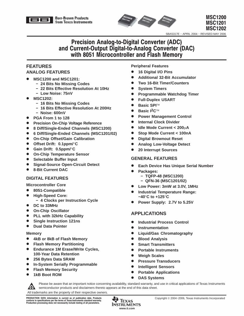
Each Device Has Unique Serial Number Packages:
− TQFP-48 (MSC1200)− QFN-36 (MSC1201/02)
Low Power: 3mW at 3.0V, 1MHz Industrial Temperature Range:
−40°C to +125°C Power Supply: 2.7V to 5.25V
APPLICATIONS
Industrial Process Control Instrumentation Liquid/Gas Chromatography Blood Analysis Smart Transmitters Portable Instruments Weigh Scales Pressure Transducers Intelligent Sensors Portable Applications DAS Systems
All trademarks are the property of their respective owners.
www.ti.com
Copyright 2004−2006, Texas Instruments Incorporated
Please be aware that an important notice concerning availability, standard warranty, and use in critical applications of Texas Instrumentssemiconductor products and disclaimers thereto appears at the end of this data sheet.
%&'() ' *! * + , *! * ! * '- (! ", " * !,
#$#$#$$SBAS317E − APRIL 2004 − REVISED MAY 2006
www.ti.com
2
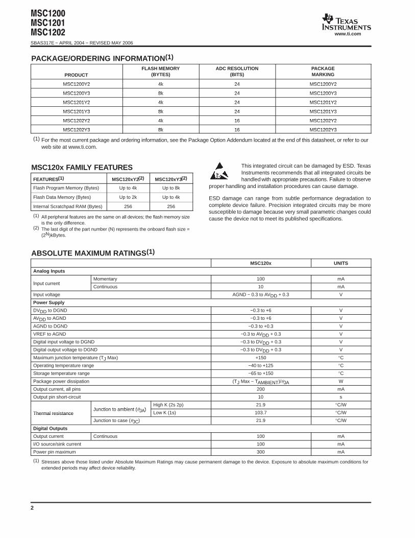
PACKAGE/ORDERING INFORMATION (1)
PRODUCTFLASH MEMORY
(BYTES)ADC RESOLUTION
(BITS)PACKAGEMARKING
MSC1200Y2 4k 24 MSC1200Y2MSC1200Y2 4k 24 MSC1200Y2
MSC1200Y3 8k 24 MSC1200Y3MSC1200Y3 8k 24 MSC1200Y3
MSC1201Y2 4k 24 MSC1201Y2MSC1201Y2 4k 24 MSC1201Y2
MSC1201Y3 8k 24 MSC1201Y3MSC1201Y3 8k 24 MSC1201Y3
MSC1202Y2 4k 16 MSC1202Y2MSC1202Y2 4k 16 MSC1202Y2
MSC1202Y3 8k 16 MSC1202Y3MSC1202Y3 8k 16 MSC1202Y3
(1) For the most current package and ordering information, see the Package Option Addendum located at the end of this datasheet, or refer to ourweb site at www.ti.com.
MSC120x FAMILY FEATURESFEATURES(1) MSC120xY2(2) MSC120xY3(2)
Flash Program Memory (Bytes) Up to 4k Up to 8k
Flash Data Memory (Bytes) Up to 2k Up to 4k
Internal Scratchpad RAM (Bytes) 256 256
(1) All peripheral features are the same on all devices; the flash memory sizeis the only difference.
(2) The last digit of the part number (N) represents the onboard flash size =(2N)kBytes.
This integrated circuit can be damaged by ESD. TexasInstruments recommends that all integrated circuits behandled with appropriate precautions. Failure to observe
proper handling and installation procedures can cause damage.
ESD damage can range from subtle performance degradation tocomplete device failure. Precision integrated circuits may be moresusceptible to damage because very small parametric changes couldcause the device not to meet its published specifications.
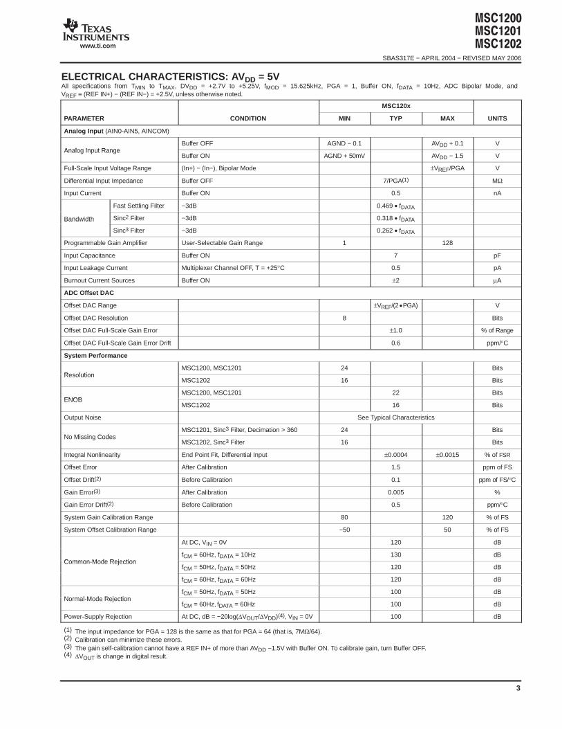
ABSOLUTE MAXIMUM RATINGS (1)
MSC120x UNITS
Analog Inputs
Input currentMomentary 100 mA
Input currentContinuous 10 mA
Input voltage AGND − 0.3 to AVDD + 0.3 V
Power Supply
DVDD to DGND −0.3 to +6 V
AVDD to AGND −0.3 to +6 V
AGND to DGND −0.3 to +0.3 V
VREF to AGND −0.3 to AVDD + 0.3 V
Digital input voltage to DGND −0.3 to DVDD + 0.3 V
Digital output voltage to DGND −0.3 to DVDD + 0.3 V
Maximum junction temperature (TJ Max) +150 °C
Operating temperature range −40 to +125 °C
Storage temperature range −65 to +150 °C
Package power dissipation (TJ Max − TAMBIENT)/JA W
Output current, all pins 200 mA
Output pin short-circuit 10 s
Junction to ambient (JA)High K (2s 2p) 21.9 °C/W
Thermal resistanceJunction to ambient (JA)
Low K (1s) 103.7 °C/WThermal resistance
Junction to case (JC) 21.9 °C/W
Digital Outputs
Output current Continuous 100 mA
I/O source/sink current 100 mA
Power pin maximum 300 mA
(1) Stresses above those listed under Absolute Maximum Ratings may cause permanent damage to the device. Exposure to absolute maximum conditions forextended periods may affect device reliability.
#$#$#$$
SBAS317E − APRIL 2004 − REVISED MAY 2006
www.ti.com
3
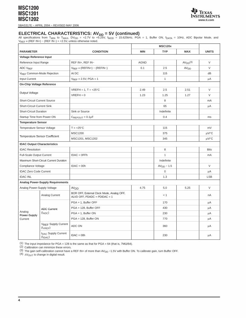
ELECTRICAL CHARACTERISTICS: AV DD = 5V All specifications from TMIN to TMAX, DVDD = +2.7V to +5.25V, fMOD = 15.625kHz, PGA = 1, Buffer ON, fDATA = 10Hz, ADC Bipolar Mode, andVREF ≡ (REF IN+) − (REF IN−) = +2.5V, unless otherwise noted.
MSC120x
PARAMETER CONDITION MIN TYP MAX UNITS
Analog Input (AIN0-AIN5, AINCOM)
Analog Input RangeBuffer OFF AGND − 0.1 AVDD + 0.1 V
Analog Input RangeBuffer ON AGND + 50mV AVDD − 1.5 V
Full-Scale Input Voltage Range (In+) − (In−), Bipolar Mode ±VREF/PGA V
Differential Input Impedance Buffer OFF 7/PGA(1) MΩ
Input Current Buffer ON 0.5 nA
Fast Settling Filter −3dB 0.469 • fDATA
Bandwidth Sinc2 Filter −3dB 0.318 • fDATABandwidth
Sinc3 Filter −3dB 0.262 • fDATA
Programmable Gain Amplifier User-Selectable Gain Range 1 128
Input Capacitance Buffer ON 7 pF
Input Leakage Current Multiplexer Channel OFF, T = +25°C 0.5 pA
Burnout Current Sources Buffer ON ±2 µA
ADC Offset DAC
Offset DAC Range ±VREF/(2 •PGA) V
Offset DAC Resolution 8 Bits
Offset DAC Full-Scale Gain Error ±1.0 % of Range
Offset DAC Full-Scale Gain Error Drift 0.6 ppm/°C
System Performance
ResolutionMSC1200, MSC1201 24 Bits
ResolutionMSC1202 16 Bits
ENOBMSC1200, MSC1201 22 Bits
ENOBMSC1202 16 Bits
Output Noise See Typical Characteristics
No Missing CodesMSC1201, Sinc3 Filter, Decimation > 360 24 Bits
No Missing CodesMSC1202, Sinc3 Filter 16 Bits
Integral Nonlinearity End Point Fit, Differential Input ±0.0004 ±0.0015 % of FSR
Offset Error After Calibration 1.5 ppm of FS
Offset Drift(2) Before Calibration 0.1 ppm of FS/°C
Gain Error(3) After Calibration 0.005 %
Gain Error Drift(2) Before Calibration 0.5 ppm/°C
System Gain Calibration Range 80 120 % of FS
System Offset Calibration Range −50 50 % of FS
At DC, VIN = 0V 120 dB
Common-Mode RejectionfCM = 60Hz, fDATA = 10Hz 130 dB
Common-Mode RejectionfCM = 50Hz, fDATA = 50Hz 120 dB
fCM = 60Hz, fDATA = 60Hz 120 dB
Normal-Mode RejectionfCM = 50Hz, fDATA = 50Hz 100 dB
Normal-Mode RejectionfCM = 60Hz, fDATA = 60Hz 100 dB
Power-Supply Rejection At DC, dB = −20log(∆VOUT/∆VDD)(4), VIN = 0V 100 dB
(1) The input impedance for PGA = 128 is the same as that for PGA = 64 (that is, 7MΩ/64).(2) Calibration can minimize these errors.(3) The gain self-calibration cannot have a REF IN+ of more than AVDD −1.5V with Buffer ON. To calibrate gain, turn Buffer OFF.(4) ∆VOUT is change in digital result.
#$#$#$$SBAS317E − APRIL 2004 − REVISED MAY 2006
www.ti.com
4
ELECTRICAL CHARACTERISTICS: AV DD = 5V (continued)All specifications from TMIN to TMAX, DVDD = +2.7V to +5.25V, fMOD = 15.625kHz, PGA = 1, Buffer ON, fDATA = 10Hz, ADC Bipolar Mode, andVREF ≡ (REF IN+) − (REF IN−) = +2.5V, unless otherwise noted.
MSC120x
PARAMETER UNITSMAXTYPMINCONDITION
Voltage Reference Input
Reference Input Range REF IN+, REF IN− AGND AVDD(3) V
ADC VREF VREF ≡ (REFIN+) − (REFIN−) 0.1 2.5 AVDD V
VREF Common-Mode Rejection At DC 115 dB
Input Current VREF = 2.5V, PGA = 1 1 µA
On-Chip Voltage Reference
Output VoltageVREFH = 1, T = +25°C 2.49 2.5 2.51 V
Output VoltageVREFH = 0 1.23 1.25 1.27 V
Short-Circuit Current Source 8 mA
Short-Circuit Current Sink 65 µA
Short-Circuit Duration Sink or Source Indefinite
Startup Time from Power ON CREFOUT = 0.1µF 0.4 ms
Temperature Sensor
Temperature Sensor Voltage T = +25°C 115 mV
Temperature Sensor CoefficientMSC1200 375 µV/°C
Temperature Sensor CoefficientMSC1201, MSC1202 345 µV/°C
IDAC Output Characteristics
IDAC Resolution 8 Bits
Full-Scale Output Current IDAC = 0FFh 1 mA
Maximum Short-Circuit Current Duration Indefinite
Compliance Voltage IDAC = 00h AVDD − 1.5 V
IDAC Zero Code Current 0 µA
IDAC INL 1.3 LSB
Analog Power-Supply Requirements
Analog Power-Supply Voltage AVDD 4.75 5.0 5.25 V
Analog CurrentBOR OFF, External Clock Mode, Analog OFF,ALVD OFF, PDADC = PDIDAC = 1
< 1 nA
PGA = 1, Buffer OFF 170 µA
AnalogADC Current PGA = 128, Buffer OFF 430 µA
AnalogPower-Supply
ADC Current(IADC) PGA = 1, Buffer ON 230 µA
Power-SupplyCurrent
ADC
PGA = 128, Buffer ON 770 µACurrent
VREF Supply Current(IVREF)
ADC ON 360 µA
IDAC Supply Current(IIDAC)
IDAC = 00h 230 µA
(1) The input impedance for PGA = 128 is the same as that for PGA = 64 (that is, 7MΩ/64).(2) Calibration can minimize these errors.(3) The gain self-calibration cannot have a REF IN+ of more than AVDD −1.5V with Buffer ON. To calibrate gain, turn Buffer OFF.(4) ∆VOUT is change in digital result.

#$#$#$$
SBAS317E − APRIL 2004 − REVISED MAY 2006
www.ti.com
5
ELECTRICAL CHARACTERISTICS: AV DD = 3V All specifications from TMIN to TMAX, DVDD = +2.7V to +5.25V, fMOD = 15.625kHz, PGA = 1, Buffer ON, fDATA = 10Hz, ADC Bipolar Mode, andVREF ≡ (REF IN+) − (REF IN−) = +1.25V, unless otherwise noted.
MSC120x
PARAMETER CONDITIONS MIN TYP MAX UNITS
Analog Input (AIN0-AIN5, AINCOM)
Analog Input RangeBuffer OFF AGND − 0.1 AVDD + 0.1 V
Analog Input RangeBuffer ON AGND + 50mV AVDD − 1.5 V
Full-Scale Input Voltage Range (In+) − (In−), Bipolar Mode ±VREF/PGA V
Differential Input Impedance Buffer OFF 7/PGA(1) MΩ
Input Current Buffer ON 0.5 nA
Fast Settling Filter −3dB 0.469 • fDATA
Bandwidth Sinc2 Filter −3dB 0.318 • fDATABandwidth
Sinc3 Filter −3dB 0.262 • fDATA
Programmable Gain Amplifier User-Selectable Gain Range 1 128
Input Capacitance Buffer ON 7 pF
Input Leakage Current Multiplexer Channel Off, T = +25°C 0.5 pA
Burnout Current Sources Buffer ON ±2 µA
ADC Offset DAC
Offset DAC Range ±VREF/(2•PGA) V
Offset DAC Resolution 8 Bits
Offset DAC Full-Scale Gain Error ±1.5 % of Range
Offset DAC Full-Scale Gain Error Drift 0.6 ppm/°C
System Performance
ResolutionMSC1200, MSC1201 24 Bits
ResolutionMSC1202 16 Bits
ENOBMSC1200, MSC1201 22 Bits
ENOBMSC1202 16 Bits
Output Noise See Typical Characteristics
No Missing Codes
MSC1200, MSC1201, Sinc3 Filter,Decimation > 360
24 BitsNo Missing Codes
MSC1202, Sinc3 Filter 16 Bits
Integral Nonlinearity End Point Fit, Differential Input ±0.0004 ±0.0015 % of FSR
Offset Error After Calibration 1.3 ppm of FS
Offset Drift(2) Before Calibration 0.1 ppm of FS/°C
Gain Error(3) After Calibration 0.005 %
Gain Error Drift(2) Before Calibration 0.5 ppm/°C
System Gain Calibration Range 80 120 % of FS
System Offset Calibration Range −50 50 % of FS
At DC, VIN = 0V 130 dB
Common-Mode RejectionfCM = 60Hz, fDATA = 10Hz 130 dB
Common-Mode RejectionfCM = 50Hz, fDATA = 50Hz 120 dB
fCM = 60Hz, fDATA = 60Hz 120 dB
Normal-Mode RejectionfSIG = 50Hz, fDATA = 50Hz 100 dB
Normal-Mode RejectionfSIG = 60Hz, fDATA = 60Hz 100 dB
Power-Supply Rejection At DC, dB = −20log(∆VOUT/∆VDD)(4), VIN = 0V 88 dB
(1) The input impedance for PGA = 128 is the same as that for PGA = 64 (that is, 7MΩ/64).(2) Calibration can minimize these errors.(3) The gain self-calibration cannot have a REF IN+ of more than AVDD −1.5V with Buffer ON. To calibrate gain, turn Buffer OFF.(4) ∆VOUT is change in digital result.
#$#$#$$SBAS317E − APRIL 2004 − REVISED MAY 2006
www.ti.com
6
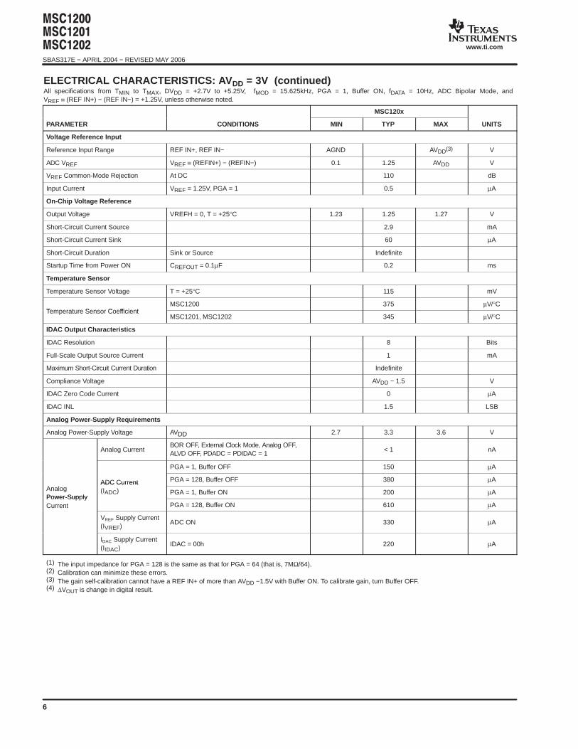
ELECTRICAL CHARACTERISTICS: AV DD = 3V (continued)All specifications from TMIN to TMAX, DVDD = +2.7V to +5.25V, fMOD = 15.625kHz, PGA = 1, Buffer ON, fDATA = 10Hz, ADC Bipolar Mode, andVREF ≡ (REF IN+) − (REF IN−) = +1.25V, unless otherwise noted.
MSC120x
PARAMETER UNITSMAXTYPMINCONDITIONS
Voltage Reference Input
Reference Input Range REF IN+, REF IN− AGND AVDD(3) V
ADC VREF VREF ≡ (REFIN+) − (REFIN−) 0.1 1.25 AVDD V
VREF Common-Mode Rejection At DC 110 dB
Input Current VREF = 1.25V, PGA = 1 0.5 µA
On-Chip Voltage Reference
Output Voltage VREFH = 0, T = +25°C 1.23 1.25 1.27 V
Short-Circuit Current Source 2.9 mA
Short-Circuit Current Sink 60 µA
Short-Circuit Duration Sink or Source Indefinite
Startup Time from Power ON CREFOUT = 0.1µF 0.2 ms
Temperature Sensor
Temperature Sensor Voltage T = +25°C 115 mV
Temperature Sensor CoefficientMSC1200 375 µV/°C
Temperature Sensor CoefficientMSC1201, MSC1202 345 µV/°C
IDAC Output Characteristics
IDAC Resolution 8 Bits
Full-Scale Output Source Current 1 mA
Maximum Short-Circuit Current Duration Indefinite
Compliance Voltage AVDD − 1.5 V
IDAC Zero Code Current 0 µA
IDAC INL 1.5 LSB
Analog Power-Supply Requirements
Analog Power-Supply Voltage AVDD 2.7 3.3 3.6 V
Analog CurrentBOR OFF, External Clock Mode, Analog OFF,ALVD OFF, PDADC = PDIDAC = 1
< 1 nA
PGA = 1, Buffer OFF 150 µA
AnalogADC Current PGA = 128, Buffer OFF 380 µA
AnalogPower-Supply
ADC Current(IADC) PGA = 1, Buffer ON 200 µA
Power-SupplyCurrent
ADC
PGA = 128, Buffer ON 610 µACurrent
VREF Supply Current(IVREF)
ADC ON 330 µA
IDAC Supply Current(IIDAC)
IDAC = 00h 220 µA
(1) The input impedance for PGA = 128 is the same as that for PGA = 64 (that is, 7MΩ/64).(2) Calibration can minimize these errors.(3) The gain self-calibration cannot have a REF IN+ of more than AVDD −1.5V with Buffer ON. To calibrate gain, turn Buffer OFF.(4) ∆VOUT is change in digital result.
#$#$#$$
SBAS317E − APRIL 2004 − REVISED MAY 2006
www.ti.com
7
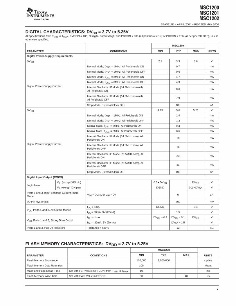
DIGITAL CHARACTERISTICS: DV DD = 2.7V to 5.25VAll specifications from TMIN to TMAX, FMCON = 10h, all digital outputs high, and PDCON = 00h (all peripherals ON) or PDCON = FFh (all peripherals OFF), unlessotherwise specified.
MSC120x
PARAMETER CONDITIONS MIN TYP MAX UNITS
Digital Power-Supply Requirements
DVDD 2.7 3.3 3.6 V
Normal Mode, fOSC = 1MHz, All Peripherals ON 0.7 mA
Normal Mode, fOSC = 1MHz, All Peripherals OFF 0.6 mA
Normal Mode, fOSC = 8MHz, All Peripherals ON 4.7 mA
Digital Power-Supply Current
Normal Mode, fOSC = 8MHz, All Peripherals OFF 4.3 mA
Digital Power-Supply Current Internal Oscillator LF Mode (14.8MHz nominal),All Peripherals ON
8.6 mA
Internal Oscillator LF Mode (14.8MHz nominal),All Peripherals OFF
7.9 mA
Stop Mode, External Clock OFF 100 nA
DVDD 4.75 5.0 5.25 V
Normal Mode, fOSC = 1MHz, All Peripherals ON 1.4 mA
Normal Mode, fOSC = 1MHz, All Peripherals OFF 1.3 mA
Normal Mode, fOSC = 8MHz, All Peripherals ON 9.3 mA
Normal Mode, fOSC = 8MHz, All Peripherals OFF 8.6 mA
Digital Power-Supply Current
Internal Oscillator LF Mode (14.8MHz nom), AllPeripherals ON
18 mA
Digital Power-Supply Current Internal Oscillator LF Mode (14.8MHz nom), AllPeripherals OFF
16 mA
Internal Oscillator HF Mode (29.5MHz nom), AllPeripherals ON
33 mA
Internal Oscillator HF Mode (29.5MHz nom), AllPeripherals OFF
31 mA
Stop Mode, External Clock OFF 100 nA
Digital Input/Output (CMOS)
Logic LevelVIH (except XIN pin) 0.6 • DVDD DVDD V
Logic LevelVIL (except XIN pin) DGND 0.2 • DVDD V
Ports 1 and 3, Input Leakage Current, InputMode
VIH = DVDD or VIH = 0V 0 µA
I/O Pin Hysteresis 700 mV
VOL, Ports 1 and 3, All Output ModesIOL = 1mA DGND 0.4 V
VOL, Ports 1 and 3, All Output ModesIOL = 30mA, 3V (20mA) 1.5 V
VOH, Ports 1 and 3, Strong Drive OutputIOH = 1mA DVDD − 0.4 DVDD − 0.1 DVDD V
VOH, Ports 1 and 3, Strong Drive OutputIOH = 30mA, 3V (20mA) DVDD − 1.5 V
Ports 1 and 3, Pull-Up Resistors Tolerance = ±25% 13 kΩ
FLASH MEMORY CHARACTERISTICS: DV DD = 2.7V to 5.25VMSC120x
PARAMETER CONDITIONS MIN TYP MAX UNITS
Flash Memory Endurance 100,000 1,000,000 cycles
Flash Memory Data Retention 100 Years
Mass and Page Erase Time Set with FER Value in FTCON, from TMIN to TMAX 10 ms
Flash Memory Write Time Set with FWR Value in FTCON 30 40 µs
#$#$#$$SBAS317E − APRIL 2004 − REVISED MAY 2006
www.ti.com
8
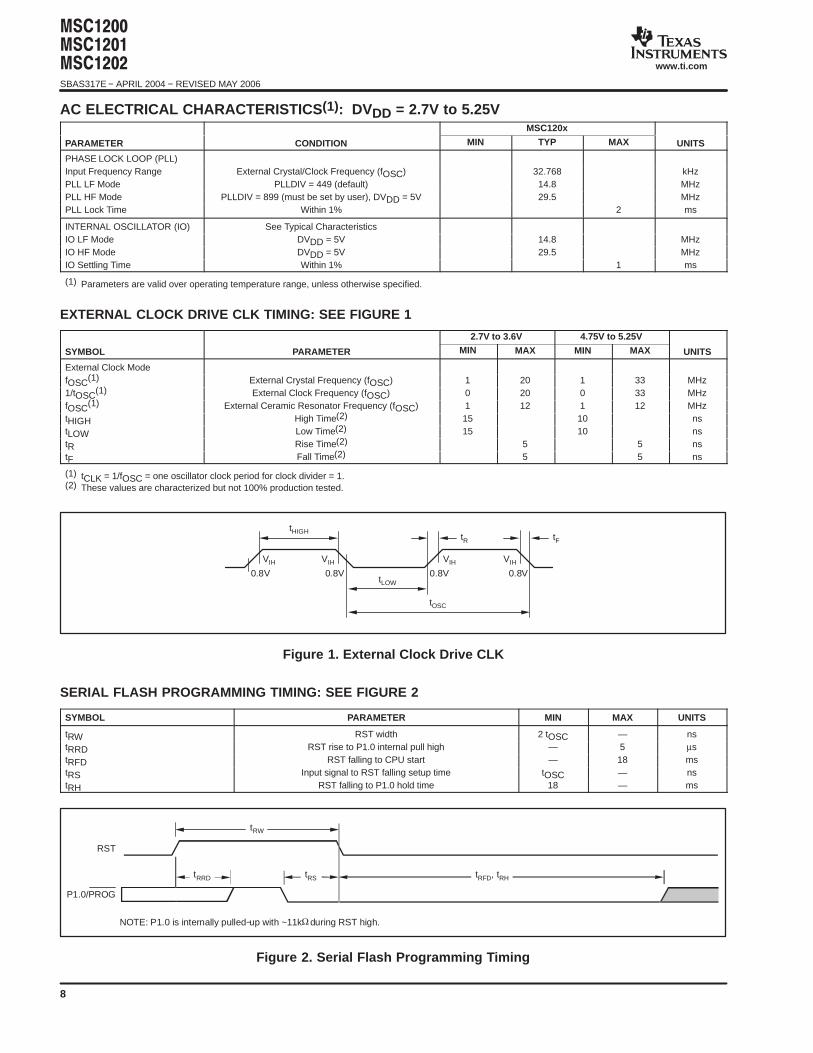
AC ELECTRICAL CHARACTERISTICS (1): DVDD = 2.7V to 5.25VMSC120x
PARAMETER CONDITION MIN TYP MAX UNITS
PHASE LOCK LOOP (PLL)Input Frequency Range External Crystal/Clock Frequency (fOSC) 32.768 kHzPLL LF Mode PLLDIV = 449 (default) 14.8 MHzPLL HF Mode PLLDIV = 899 (must be set by user), DVDD = 5V 29.5 MHzPLL Lock Time Within 1% 2 ms
INTERNAL OSCILLATOR (IO) See Typical CharacteristicsIO LF Mode DVDD = 5V 14.8 MHzIO HF Mode DVDD = 5V 29.5 MHzIO Settling Time Within 1% 1 ms
(1) Parameters are valid over operating temperature range, unless otherwise specified.
EXTERNAL CLOCK DRIVE CLK TIMING: SEE FIGURE 1
2.7V to 3.6V 4.75V to 5.25V
SYMBOL PARAMETER MIN MAX MIN MAX UNITS
External Clock ModefOSC(1) External Crystal Frequency (fOSC) 1 20 1 33 MHz1/tOSC(1) External Clock Frequency (fOSC) 0 20 0 33 MHzfOSC(1) External Ceramic Resonator Frequency (fOSC) 1 12 1 12 MHztHIGH High Time(2) 15 10 nstLOW Low Time(2) 15 10 nstR Rise Time(2) 5 5 nstF Fall Time(2) 5 5 ns
(1) tCLK = 1/fOSC = one oscillator clock period for clock divider = 1.(2) These values are characterized but not 100% production tested.
tRtHIGH
VIH VIH
0.8V 0.8V
VIH VIH
0.8V 0.8VtLOW
tOSC
tF
Figure 1. External Clock Drive CLK
SERIAL FLASH PROGRAMMING TIMING: SEE FIGURE 2
SYMBOL PARAMETER MIN MAX UNITS
tRW RST width 2 tOSC — nstRRD RST rise to P1.0 internal pull high — 5 µstRFD RST falling to CPU start — 18 mstRS Input signal to RST falling setup time tOSC — nstRH RST falling to P1.0 hold time 18 — ms
NOTE: P1.0 is internally pulled−up with ~11kΩ during RST high.
P1.0/PROG
RST
tRFD, tRHtRStRRD
tRW
Figure 2. Serial Flash Programming Timing
#$#$#$$
SBAS317E − APRIL 2004 − REVISED MAY 2006
www.ti.com
9
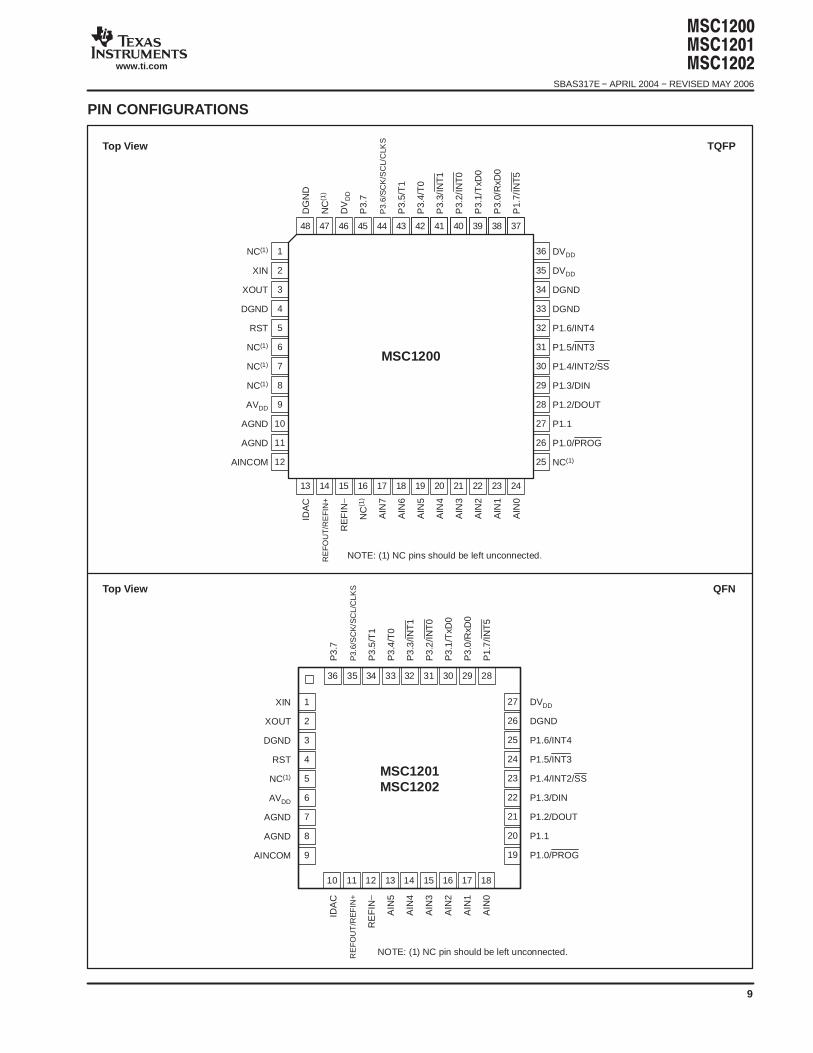
PIN CONFIGURATIONS
Top View TQFP
Top View QFN
36
35
34
33
32
31
30
29
28
27
26
25
DVDD
DVDD
DGND
DGND
P1.6/INT4
P1.5/INT3
P1.4/INT2/SS
P1.3/DIN
P1.2/DOUT
P1.1
P1.0/PROG
NC(1)
DG
ND
NC
(1)
DV
DD
P3.
7
P3.
6/S
CK
/SC
L/C
LKS
P3.
5/T
1
P3.
4/T
0
P3.
3/IN
T1
P3.
2/IN
T0
P3.
1/T
xD0
P3.
0/R
xD0
P1.
7/IN
T5
IDA
C
RE
FO
UT
/RE
FIN
+
RE
FIN
−
NC
(1)
AIN
7
AIN
6
AIN
5
AIN
4
AIN
3
AIN
2
AIN
1
AIN
0
1
2
3
4
5
6
7
8
9
10
11
12
NC(1)
XIN
XOUT
DGND
RST
NC(1)
NC(1)
NC(1)
AVDD
AGND
AGND
AINCOM
48 47 46 45 44 43 42 41 40 39 38
13 14 15 16 17 18 19 20 21 22 23
37
24
MSC1200
NOTE: (1) NC pins should be left unconnected.
P3
.7
P3.
6/S
CK
/SC
L/C
LKS
P3
.5/T
1
P3
.4/T
0
P3
.3/IN
T1
P3
.2/IN
T0
P3
.1/T
xD0
P3
.0/R
xD0
P1
.7/IN
T5
XIN
XOUT
DGND
RST
NC(1)
AVDD
AGND
AGND
AINCOM
IDA
C
RE
FO
UT
/RE
FIN
+
RE
FIN
−
AIN
5
AIN
4
AIN
3
AIN
2
AIN
1
AIN
0
DVDD
DGND
P1.6/INT4
P1.5/INT3
P1.4/INT2/SS
P1.3/DIN
P1.2/DOUT
P1.1
P1.0/PROG
NOTE: (1) NC pin should be left unconnected.
1
2
3
4
5
6
7
8
9
27
26
25
24
23
22
21
20
19
10 11 12 13 14 15 16 17 18
36 35 34 33 32 31 30 29 28
MSC1201MSC1202
#$#$#$$SBAS317E − APRIL 2004 − REVISED MAY 2006
www.ti.com
10
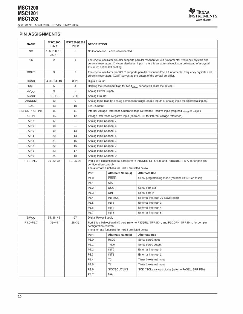
PIN ASSIGNMENTS
NAMEMSC1200
PIN #MSC1201/1202
PIN # DESCRIPTION
NC 1, 6, 7, 8, 16,25, 47
5 No Connection. Leave unconnected.
XIN 2 1 The crystal oscillator pin XIN supports parallel resonant AT-cut fundamental frequency crystals andceramic resonators. XIN can also be an input if there is an external clock source instead of a crystal.XIN must not be left floating.
XOUT 3 2 The crystal oscillator pin XOUT supports parallel resonant AT-cut fundamental frequency crystals andceramic resonators. XOUT serves as the output of the crystal amplifier.
DGND 4, 33, 34, 48 3, 26 Digital Ground
RST 5 4 Holding the reset input high for two tOSC periods will reset the device.
AVDD 9 6 Analog Power Supply
AGND 10, 11 7, 8 Analog Ground
AINCOM 12 9 Analog Input (can be analog common for single-ended inputs or analog input for differential inputs)
IDAC 13 10 IDAC Output
REFOUT/REF IN+ 14 11 Internal Voltage Reference Output/Voltage Reference Positive Input (required CREF = 0.1µF)
REF IN− 15 12 Voltage Reference Negative Input (tie to AGND for internal voltage reference)
AIN7 17 — Analog Input Channel 7
AIN6 18 — Analog Input Channel 6
AIN5 19 13 Analog Input Channel 5
AIN4 20 14 Analog Input Channel 4
AIN3 21 15 Analog Input Channel 3
AIN2 22 16 Analog Input Channel 2
AIN1 23 17 Analog Input Channel 1
AIN0 24 18 Analog Input Channel 0
P1.0−P1.7 26−32, 37 19−25, 28 Port 1 is a bidirectional I/O port (refer to P1DDRL, SFR AEh, and P1DDRH, SFR AFh, for port pinconfiguration control).The alternate functions for Port 1 are listed below.
Port Alternate Name(s) Alternate Use
P1.0 PROG Serial programming mode (must be DGND on reset)
P1.1 N/A
P1.2 DOUT Serial data out
P1.3 DIN Serial data in
P1.4 INT2/SS External interrupt 2 / Slave Select
P1.5 INT3 External interrupt 3
P1.6 INT4 External interrupt 4
P1.7 INT5 External interrupt 5
DVDD 35, 36, 46 27 Digital Power Supply
P3.0−P3.7 38−45 29−36 Port 3 is a bidirectional I/O port (refer to P3DDRL, SFR B3h, and P3DDRH, SFR B4h, for port pinconfiguration control).The alternate functions for Port 3 are listed below.
Port Alternate Name(s) Alternate Use
P3.0 RxD0 Serial port 0 input
P3.1 TxD0 Serial port 0 output
P3.2 INT0 External interrupt 0
P3.3 INT1 External interrupt 1
P3.4 T0 Timer 0 external input
P3.5 T1 Timer 1 external input
P3.6 SCK/SCL/CLKS SCK / SCL / various clocks (refer to PASEL, SFR F2h)
P3.7 N/A
#$#$#$$
SBAS317E − APRIL 2004 − REVISED MAY 2006
www.ti.com
11
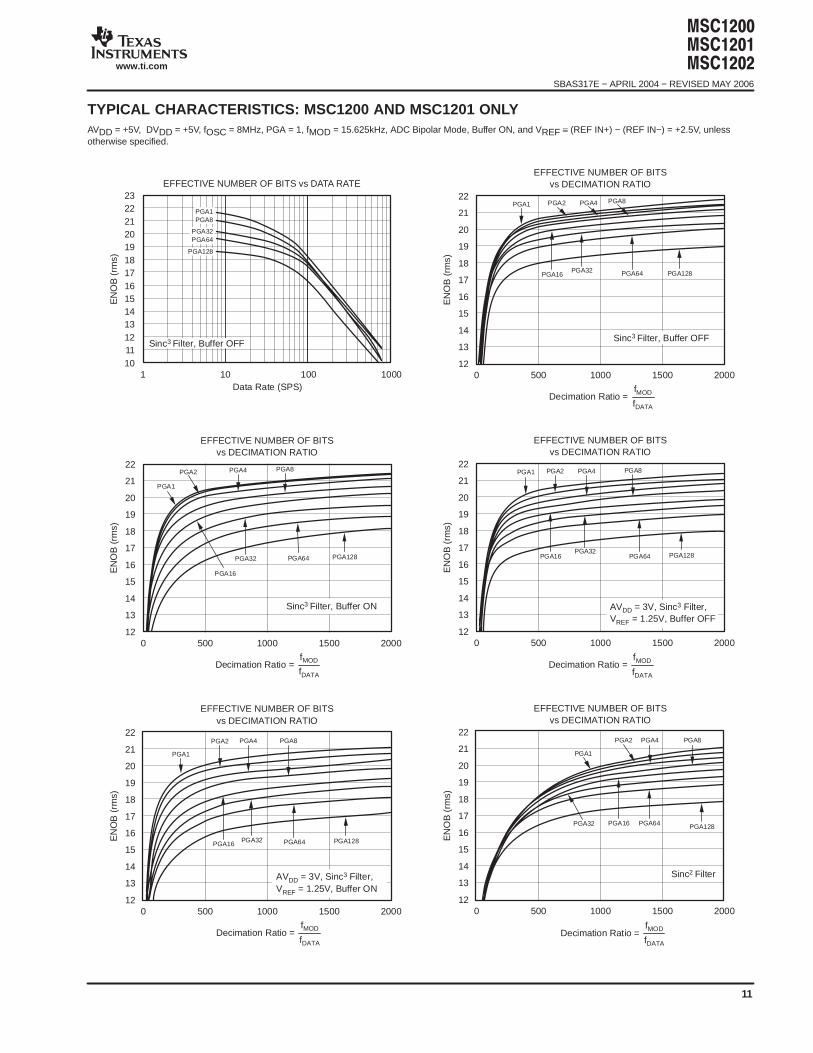
TYPICAL CHARACTERISTICS: MSC1200 AND MSC1201 ONLYAVDD = +5V, DVDD = +5V, fOSC = 8MHz, PGA = 1, fMOD = 15.625kHz, ADC Bipolar Mode, Buffer ON, and VREF ≡ (REF IN+) − (REF IN−) = +2.5V, unlessotherwise specified.
EFFECTIVE NUMBER OF BITS vs DATA RATE2322212019181716151413121110
EN
OB
(rm
s)
Data Rate (SPS)1 10 100 1000
Sinc3 Filter, Buffer OFF
PGA1PGA8
PGA32PGA64
PGA128
22
21
20
19
18
17
16
15
14
13
12
EFFECTIVE NUMBER OF BITSvs DECIMATION RATIO
Decimation Ratio =fMOD
fDATA
0 500 1000 1500 2000
PGA4
EN
OB
(rm
s)
PGA1 PGA2
PGA16
PGA8
PGA32 PGA64 PGA128
Sinc3 Filter, Buffer OFF
22
21
20
19
18
17
16
15
14
13
12
EFFECTIVE NUMBER OF BITSvs DECIMATION RATIO
0 500 1000 1500 2000
EN
OB
(rm
s)
PGA4 PGA8
PGA1
PGA2
PGA16
PGA32 PGA64 PGA128
Decimation Ratio =fMOD
fDATA
Sinc3 Filter, Buffer ON
22
21
20
19
18
17
16
15
14
13
12
EFFECTIVE NUMBER OF BITSvs DECIMATION RATIO
0 500 1000 1500 2000
EN
OB
(rm
s)
PGA4 PGA8PGA1 PGA2
PGA16PGA32
PGA64 PGA128
Decimation Ratio =fMOD
fDATA
AVDD = 3V, Sinc3 Filter,VREF = 1.25V, Buffer OFF
22
21
20
19
18
17
16
15
14
13
12
EFFECTIVE NUMBER OF BITSvs DECIMATION RATIO
0 500 1000 1500 2000
EN
OB
(rm
s)
PGA4 PGA8
PGA1
PGA2
PGA16 PGA32 PGA64 PGA128
AVDD = 3V, Sinc3 Filter,VREF = 1.25V, Buffer ON
Decimation Ratio =fMOD
fDATA
22
21
20
19
18
17
16
15
14
13
12
EFFECTIVE NUMBER OF BITSvs DECIMATION RATIO
0 500 1000 1500 2000
EN
OB
(rm
s)
PGA4 PGA8
PGA1
PGA2
PGA32 PGA128PGA16 PGA64
Decimation Ratio =fMOD
fDATA
Sinc2 Filter
#$#$#$$SBAS317E − APRIL 2004 − REVISED MAY 2006
www.ti.com
12
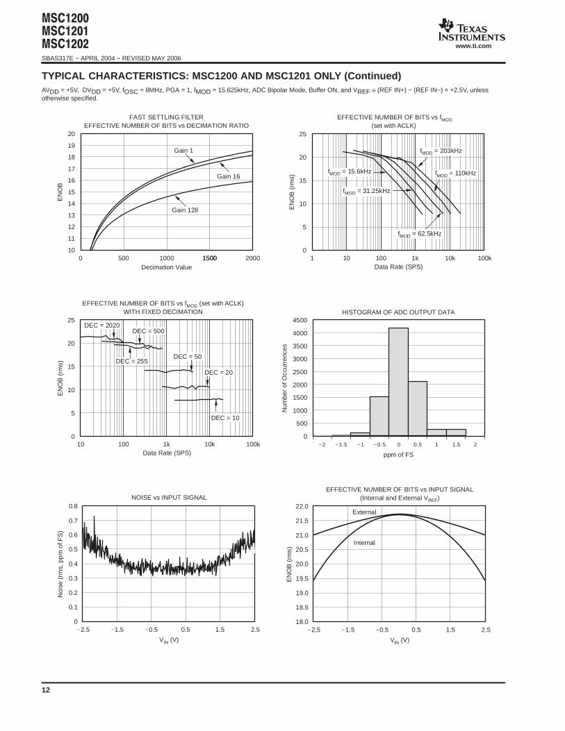
TYPICAL CHARACTERISTICS: MSC1200 AND MSC1201 ONLY (Continued)AVDD = +5V, DVDD = +5V, fOSC = 8MHz, PGA = 1, fMOD = 15.625kHz, ADC Bipolar Mode, Buffer ON, and VREF ≡ (REF IN+) − (REF IN−) = +2.5V, unlessotherwise specified.
20
19
18
17
16
15
14
13
12
11
10
FAST SETTLING FILTEREFFECTIVE NUMBER OF BITS vs DECIMATION RATIO
0 500 1000
Gain 1
Gain 16
Gain 128
1500 2000
EN
OB
1500Decimation Value
EFFECTIVE NUMBER OF BITS vs fMOD(set with ACLK)
25
20
15
10
5
0
EN
OB
(rm
s)
Data Rate (SPS)1 10 100 1k 10k 100k
fMOD = 15.6kHz
fMOD = 62.5kHz
fMOD = 203kHz
fMOD = 110kHz
fMOD = 31.25kHz
EFFECTIVE NUMBER OF BITS vs fMOD (set with ACLK)WITH FIXED DECIMATION
25
20
15
10
5
0
EN
OB
(rm
s)
Data Rate (SPS)10 100 1k 10k 100k
DEC = 2020
DEC = 255
DEC = 500
DEC = 50
DEC = 20
DEC = 10
4500
4000
3500
3000
2500
2000
1500
1000
500
0
HISTOGRAM OF ADC OUTPUT DATA
ppm of FS
−2
Num
ber
ofO
ccur
renc
es
−1.5 −1 −0.5 0 0.5 1 1.5 2
0.8
0.7
0.6
0.5
0.4
0.3
0.2
0.1
0
NOISE vs INPUT SIGNAL
VIN (V)
− 2.5 −1.5 0.5−0.5 1.5 2.5
Noi
se(r
ms,
ppm
ofF
S)
22.0
21.5
21.0
20.5
20.0
19.5
19.0
18.5
18.0
EFFECTIVE NUMBER OF BITS vs INPUT SIGNAL(Internal and External VREF)
VIN (V)
−2.5 −1.5 0.5−0.5 1.5 2.5
EN
OB
(rm
s)
External
Internal
#$#$#$$
SBAS317E − APRIL 2004 − REVISED MAY 2006
www.ti.com
13
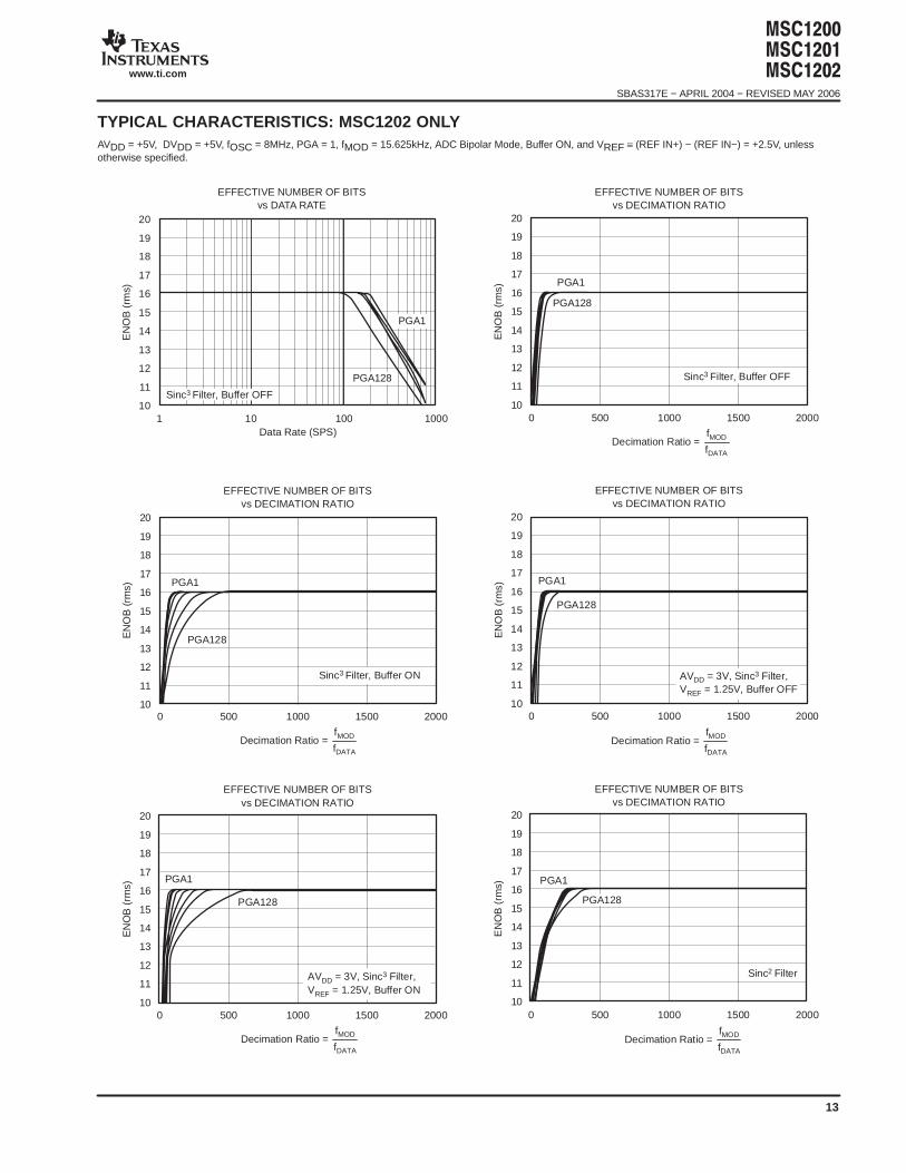
TYPICAL CHARACTERISTICS: MSC1202 ONLYAVDD = +5V, DVDD = +5V, fOSC = 8MHz, PGA = 1, fMOD = 15.625kHz, ADC Bipolar Mode, Buffer ON, and VREF ≡ (REF IN+) − (REF IN−) = +2.5V, unlessotherwise specified.
EFFECTIVE NUMBER OF BITSvs DATA RATE
20
19
18
17
16
15
14
13
12
11
10
EN
OB
(rm
s)
Data Rate (SPS)1 10 100 1000
Sinc3 Filter, Buffer OFF
PGA1
PGA128
20
19
18
17
16
15
14
13
12
11
10
EFFECTIVE NUMBER OF BITSvs DECIMATION RATIO
Decimation Ratio =fMOD
fDATA
0 500 1000 1500 2000
EN
OB
(rm
s)
PGA1
PGA128
Sinc3 Filter, Buffer OFF
20
19
18
17
16
15
14
13
12
11
10
EFFECTIVE NUMBER OF BITSvs DECIMATION RATIO
0 500 1000 1500 2000
EN
OB
(rm
s) PGA1
PGA128
Decimation Ratio =fMOD
fDATA
Sinc3 Filter, Buffer ON
20
19
18
17
16
15
14
13
12
11
10
PGA1
PGA128
EFFECTIVE NUMBER OF BITSvs DECIMATION RATIO
0 500 1000 1500 2000
EN
OB
(rm
s)
Decimation Ratio =fMOD
fDATA
AVDD = 3V, Sinc3 Filter,VREF = 1.25V, Buffer OFF
20
19
18
17
16
15
14
13
12
11
10
EFFECTIVE NUMBER OF BITSvs DECIMATION RATIO
0 500 1000 1500 2000
EN
OB
(rm
s)
PGA1
PGA128
AVDD = 3V, Sinc3 Filter,VREF = 1.25V, Buffer ON
Decimation Ratio =fMOD
fDATA
20
19
18
17
16
15
14
13
12
11
10
EFFECTIVE NUMBER OF BITSvs DECIMATION RATIO
0 500 1000 1500 2000
EN
OB
(rm
s) PGA1
Decimation Ratio =fMOD
fDATA
Sinc2 Filter
PGA128
#$#$#$$SBAS317E − APRIL 2004 − REVISED MAY 2006
www.ti.com
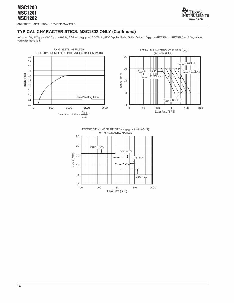
14
TYPICAL CHARACTERISTICS: MSC1202 ONLY (Continued)AVDD = +5V, DVDD = +5V, fOSC = 8MHz, PGA = 1, fMOD = 15.625kHz, ADC Bipolar Mode, Buffer ON, and VREF ≡ (REF IN+) − (REF IN−) = +2.5V, unlessotherwise specified.
20
19
18
17
16
15
14
13
12
11
10
FAST SETTLING FILTEREFFECTIVE NUMBER OF BITS vs DECIMATION RATIO
0 500 1000 1500 2000
EN
OB
(rm
s)
1500
Decimation Ratio =fMOD
fDATA
Fast Settling Filter
EFFECTIVE NUMBER OF BITS vs fMOD(set with ACLK)
20
16
12
8
4
EN
OB
(rm
s)
Data Rate (SPS)1 10 100 1k 10k 100k
fMOD = 15.6kHz
fMOD = 62.5kHz
fMOD = 203kHz
fMOD = 110kHz
fMOD = 31.25kHz
EFFECTIVE NUMBER OF BITS vs fMOD (set with ACLK)WITH FIXED DECIMATION
25
20
15
10
5
0
EN
OB
(rm
s)
Data Rate (SPS)10 100 1k 10k 100k
DEC = 50DEC > 100
DEC = 20
DEC = 10
#$#$#$$
SBAS317E − APRIL 2004 − REVISED MAY 2006
www.ti.com
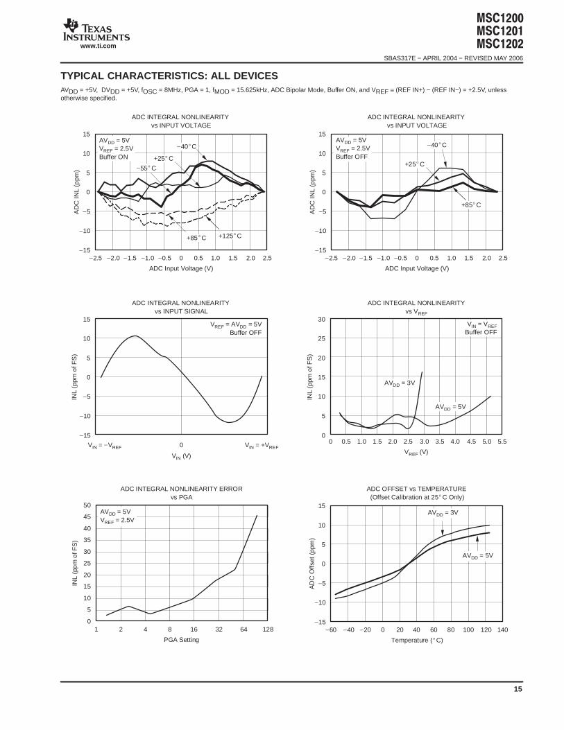
15
TYPICAL CHARACTERISTICS: ALL DEVICESAVDD = +5V, DVDD = +5V, fOSC = 8MHz, PGA = 1, fMOD = 15.625kHz, ADC Bipolar Mode, Buffer ON, and VREF ≡ (REF IN+) − (REF IN−) = +2.5V, unlessotherwise specified.
15
10
5
0
−5
−10
−15
ADC INTEGRAL NONLINEARITYvs INPUT VOLTAGE
ADC Input Voltage (V)
−2.5 −1.0 −0.5 1.00.5 2.0 2.5−1.5−2.0 0 1.5
AD
CIN
L(p
pm)
+125C+85C
+25C−55C
−40CAVDD = 5VVREF = 2.5VBuffer ON
15
10
5
0
−5
−10
−15
ADC INTEGRAL NONLINEARITYvs INPUT VOLTAGE
ADC Input Voltage (V)
−2.5 −1.0 −0.5 1.00.5 2.0 2.5−1.5−2.0 0 1.5
AD
CIN
L(p
pm)
+85C
+25C
−40CAVDD = 5VVREF = 2.5VBuffer OFF
15
10
5
0
−5
−10
−15
ADC INTEGRAL NONLINEARITYvs INPUT SIGNAL
VIN (V)
VIN = −VREF 0 VIN = +VREF
INL
(ppm
ofF
S)
VREF = AVDD = 5VBuffer OFF
30
25
20
15
10
5
0
ADC INTEGRAL NONLINEARITYvs VREF
VREF (V)
0 0.5 1.0 1.5 2.0 2.5 3.0 3.5 4.0 4.5 5.0 5.5
INL
(ppm
ofF
S)
VIN = VREFBuffer OFF
AVDD = 3V
AVDD = 5V
ADC INTEGRAL NONLINEARITY ERRORvs PGA
PGA Setting
INL
(pp
mo
fFS
)
1 42 168 1286432
50
45
40
35
30
25
20
15
10
5
0
AVDD = 5VVREF = 2.5V
15
10
5
0
−5
−10
−15
ADC OFFSET vs TEMPERATURE(Offset Calibration at 25C Only)
Temperature (C)
−60 0 20 8060 120 140−20−40 40 100
AD
CO
ffset
(ppm
)
AVDD = 5V
AVDD = 3V
#$#$#$$SBAS317E − APRIL 2004 − REVISED MAY 2006
www.ti.com
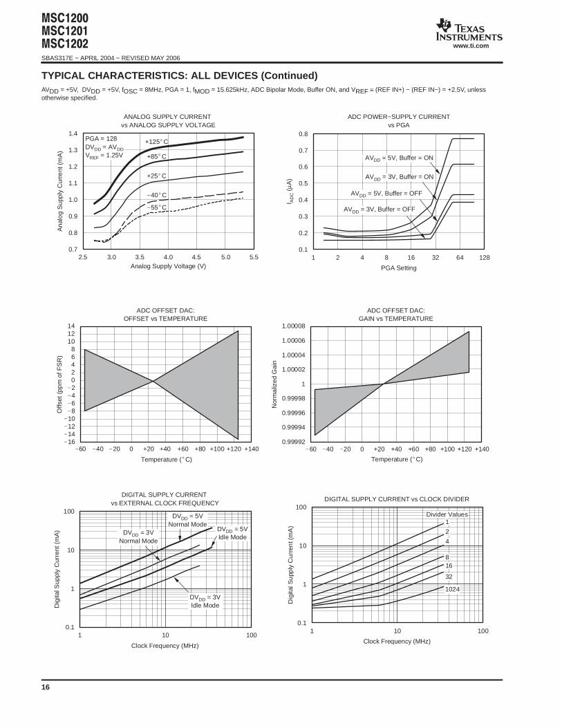
16
TYPICAL CHARACTERISTICS: ALL DEVICES (Continued)AVDD = +5V, DVDD = +5V, fOSC = 8MHz, PGA = 1, fMOD = 15.625kHz, ADC Bipolar Mode, Buffer ON, and VREF ≡ (REF IN+) − (REF IN−) = +2.5V, unlessotherwise specified.
1.4
1.3
1.2
1.1
1.0
0.9
0.8
0.7
ANALOG SUPPLY CURRENTvs ANALOG SUPPLY VOLTAGE
Analog Supply Voltage (V)2.5 3.5 4.5 5.53.0 4.0 5.0
An
alo
gS
upp
lyC
urr
ent
(mA
)
−55C
−40C
+25C
+85C
+125CPGA = 128DVDD = AVDDVREF = 1.25V
0.8
0.7
0.6
0.5
0.4
0.3
0.2
0.1
ADC POWER−SUPPLY CURRENTvs PGA
PGA Setting
1 82 4 3216 12864
I AD
C(µ
A)
AVDD = 5V, Buffer = ON
AVDD = 5V, Buffer = OFF
AVDD = 3V, Buffer = ON
AVDD = 3V, Buffer = OFF
141210
86420
−2−4−6−8
−10−12−14−16
ADC OFFSET DAC:OFFSET vs TEMPERATURE
Offs
et(p
pm
ofF
SR
)
Temperature (C)
−60 −40 −20 0 +20 +40 +60 +80 +100 +120 +140
1.00008
1.00006
1.00004
1.00002
1
0.99998
0.99996
0.99994
0.99992
ADC OFFSET DAC:GAIN vs TEMPERATURE
Nor
ma
lized
Gai
n
Temperature (C)
−60 −40 −20 +140+20 +40 +60 +80 +100 +1200
DIGITAL SUPPLY CURRENTvs EXTERNAL CLOCK FREQUENCY
Clock Frequency (MHz)
Dig
italS
uppl
yC
urre
nt(m
A)
1 10 100
100
10
1
0.1
DVDD = 5VNormal Mode
DVDD = 3VNormal Mode
DVDD = 3VIdle Mode
DVDD = 5VIdle Mode
DIGITAL SUPPLY CURRENT vs CLOCK DIVIDER
Clock Frequency (MHz)
Dig
italS
upp
lyC
urr
ent(
mA
)
1 10 100
100
10
1
0.1
1024
Divider Values
2
1
4
816
32
#$#$#$$
SBAS317E − APRIL 2004 − REVISED MAY 2006
www.ti.com
17
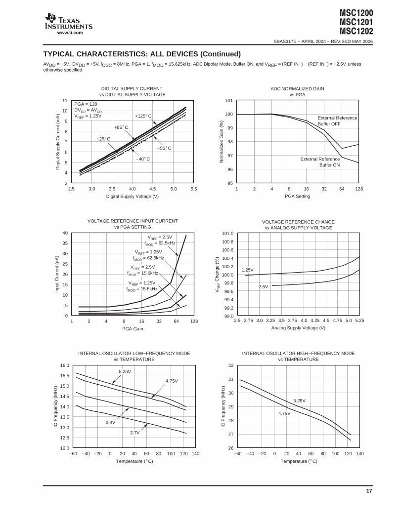
TYPICAL CHARACTERISTICS: ALL DEVICES (Continued)AVDD = +5V, DVDD = +5V, fOSC = 8MHz, PGA = 1, fMOD = 15.625kHz, ADC Bipolar Mode, Buffer ON, and VREF ≡ (REF IN+) − (REF IN−) = +2.5V, unlessotherwise specified.
11
10
9
8
7
6
5
4
3
DIGITAL SUPPLY CURRENTvs DIGITAL SUPPLY VOLTAGE
Digital Supply Voltage (V)
2.5 3.5 4.5 5.53.0 4.0 5.0
Dig
italS
upp
lyC
urre
nt(m
A)
−55C
−40C
+25C
+85C
+125C
PGA = 128DVDD = AVDDVREF = 1.25V
ADC NORMALIZED GAINvs PGA
PGA Setting
Nor
mal
ize
dG
ain
(%)
1 42 168 1286432
101
100
99
98
97
96
95
External ReferenceBuffer ON
External ReferenceBuffer OFF
40
35
30
25
20
15
10
5
0
VOLTAGE REFERENCE INPUT CURRENTvs PGA SETTING
PGA Gain
1 1282 4 8 16 32 64
Inpu
tCur
rent
(µA
)
VREF = 2.5VfMOD = 62.5kHz
VREF = 1.25VfMOD = 62.5kHz
VREF = 2.5VfMOD = 15.6kHz
VREF = 1.25VfMOD = 15.6kHz
101.0
100.8
100.6
100.4
100.2
100.0
99.8
99.6
99.4
99.2
99.0
VOLTAGE REFERENCE CHANGEvs ANALOG SUPPLY VOLTAGE
Analog Supply Voltage (V)
2.5 2.75 3.0 3.25 3.5 3.75 4.0 4.25 4.5 4.75 5.0 5.25
VR
EF
Cha
nge
(%)
2.5V
1.25V
16.0
15.5
15.0
14.5
14.0
13.5
13.0
12.5
12.0
INTERNAL OSCILLATOR LOW−FREQUENCY MODEvs TEMPERATURE
Temperature (C)
−60 0 20 8060 120 140−20−40 40 100
IOF
req
uen
cy(M
Hz)
5.25V
2.7V
3.3V
4.75V
32
31
30
29
28
27
26
INTERNAL OSCILLATOR HIGH−FREQUENCY MODEvs TEMPERATURE
Temperature (C)
−60 0 20 8060 120 140−20−40 40 100
IOF
req
uen
cy(M
Hz)
5.25V
4.75V
#$#$#$$SBAS317E − APRIL 2004 − REVISED MAY 2006
www.ti.com
18
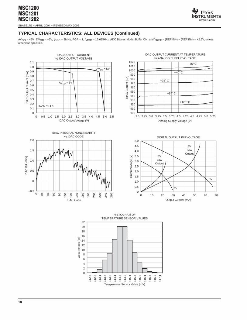
TYPICAL CHARACTERISTICS: ALL DEVICES (Continued)AVDD = +5V, DVDD = +5V, fOSC = 8MHz, PGA = 1, fMOD = 15.625kHz, ADC Bipolar Mode, Buffer ON, and VREF ≡ (REF IN+) − (REF IN−) = +2.5V, unlessotherwise specified.
1.1
1.0
0.9
0.8
0.7
0.6
0.5
0.4
0.3
0.2
0.1
0
IDAC OUTPUT CURRENTvs IDAC OUTPUT VOLTAGE
IDAC Output Votage (V)0 0.5 1.0 1.5 2.0 2.5 5.55.04.54.03.53.0
IDA
CO
utp
utC
urre
nt(m
A)
AVDD = 5V
IDAC = FFh
AVDD = 3V
1020
1010
1000
990
980
970
960
950
940
930
920
910
900
IDAC OUTPUT CURRENT AT TEMPERATUREvs ANALOG SUPPLY VOLTAGE
Analog Supply Voltage (V)
2.5 3.53.0 4.0 4.5 5.0 5.252.75 3.25 3.75 4.25 4.75
IDA
CC
urre
nt(µ
A)
+85C
+125C
+25C
−40C
−55C
2.0
1.5
1.0
0.5
0
−0.5
IDAC INTEGRAL NONLINEARITYvs IDAC CODE
IDAC Code
0 20 40 60 80
100
120
140
160
180
200
220
240
260
IDA
CIN
L(B
its)
DIGITAL OUTPUT PIN VOLTAGE
Output Current (mA)
Out
putV
olta
ge(V
)
0 2010 4030 706050
5.0
4.5
4.0
3.5
3.0
2.5
2.0
1.5
1.0
0.5
0
3VLow
Output
5VLow
Output
5V
3V
22
20
18
16
14
12
10
8
6
4
2
0
HISTOGRAM OFTEMPERATURE SENSOR VALUES
Temperature Sensor Value (mV)
112.
4
112.
7
113.
1
113.
4
113.
7
114.
1
114.
4
114.
7
115.
1
115.
4
115.
7
116.
1
116.
4
116.
7
117.
1
Occ
urre
nce
s(%
)
#$#$#$$
SBAS317E − APRIL 2004 − REVISED MAY 2006
www.ti.com
19
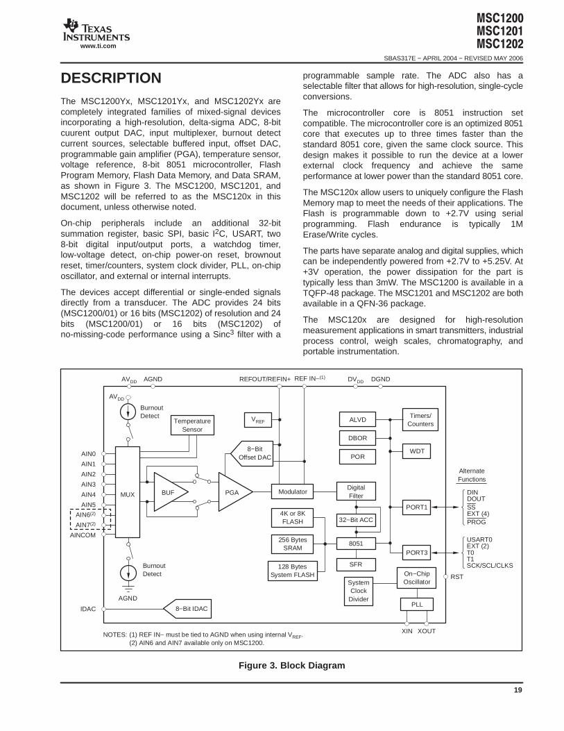
DESCRIPTIONThe MSC1200Yx, MSC1201Yx, and MSC1202Yx arecompletely integrated families of mixed-signal devicesincorporating a high-resolution, delta-sigma ADC, 8-bitcuurent output DAC, input multiplexer, burnout detectcurrent sources, selectable buffered input, offset DAC,programmable gain amplifier (PGA), temperature sensor,voltage reference, 8-bit 8051 microcontroller, FlashProgram Memory, Flash Data Memory, and Data SRAM,as shown in Figure 3. The MSC1200, MSC1201, andMSC1202 will be referred to as the MSC120x in thisdocument, unless otherwise noted.
On-chip peripherals include an additional 32-bitsummation register, basic SPI, basic I2C, USART, two8-bit digital input/output ports, a watchdog timer,low-voltage detect, on-chip power-on reset, brownoutreset, timer/counters, system clock divider, PLL, on-chiposcillator, and external or internal interrupts.
The devices accept differential or single-ended signalsdirectly from a transducer. The ADC provides 24 bits(MSC1200/01) or 16 bits (MSC1202) of resolution and 24bits (MSC1200/01) or 16 bits (MSC1202) ofno-missing-code performance using a Sinc3 filter with a
programmable sample rate. The ADC also has aselectable filter that allows for high-resolution, single-cycleconversions.
The microcontroller core is 8051 instruction setcompatible. The microcontroller core is an optimized 8051core that executes up to three times faster than thestandard 8051 core, given the same clock source. Thisdesign makes it possible to run the device at a lowerexternal clock frequency and achieve the sameperformance at lower power than the standard 8051 core.
The MSC120x allow users to uniquely configure the FlashMemory map to meet the needs of their applications. TheFlash is programmable down to +2.7V using serialprogramming. Flash endurance is typically 1MErase/Write cycles.
The parts have separate analog and digital supplies, whichcan be independently powered from +2.7V to +5.25V. At+3V operation, the power dissipation for the part istypically less than 3mW. The MSC1200 is available in aTQFP-48 package. The MSC1201 and MSC1202 are bothavailable in a QFN-36 package.
The MSC120x are designed for high-resolutionmeasurement applications in smart transmitters, industrialprocess control, weigh scales, chromatography, andportable instrumentation.
MUX
AVDD
BUF PGA
VREF
Modulator
4K or 8KFLASH
256 BytesSRAM
128 BytesSystem FLASH
DigitalFilter
32−Bit ACC
8051
SFR
ALVD
DBOR
POR
SystemClock
Divider
PORT1
WDT
AlternateFunctions
Timers/Counters
PLL
PORT3
DINDOUTSSEXT (4)PROG
USART0EXT (2)T0T1SCK/SCL/CLKS
On−ChipOscillator
8−BitOffset DAC
8−Bit IDAC
BurnoutDetect
AIN0
AIN1
AIN2
AIN3
AIN4
AIN5
AIN6(2)
AIN7(2)
AINCOM
IDAC
AGND REFOUT/REFIN+ DVDD DGND
XIN XOUT
TemperatureSensor
BurnoutDetect
RST
AGND
AVDD
REF IN−(1)
(1) REF IN− must be tied to AGND when using internal VREF.(2) AIN6 and AIN7 available only on MSC1200.
NOTES:
Figure 3. Block Diagram
#$#$#$$SBAS317E − APRIL 2004 − REVISED MAY 2006
www.ti.com
20
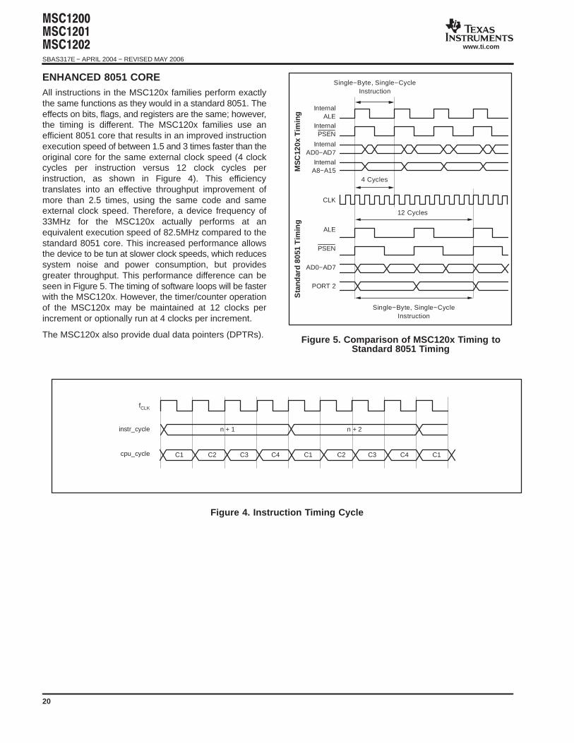
ENHANCED 8051 COREAll instructions in the MSC120x families perform exactlythe same functions as they would in a standard 8051. Theeffects on bits, flags, and registers are the same; however,the timing is different. The MSC120x families use anefficient 8051 core that results in an improved instructionexecution speed of between 1.5 and 3 times faster than theoriginal core for the same external clock speed (4 clockcycles per instruction versus 12 clock cycles perinstruction, as shown in Figure 4). This efficiencytranslates into an effective throughput improvement ofmore than 2.5 times, using the same code and sameexternal clock speed. Therefore, a device frequency of33MHz for the MSC120x actually performs at anequivalent execution speed of 82.5MHz compared to thestandard 8051 core. This increased performance allowsthe device to be tun at slower clock speeds, which reducessystem noise and power consumption, but providesgreater throughput. This performance difference can beseen in Figure 5. The timing of software loops will be fasterwith the MSC120x. However, the timer/counter operationof the MSC120x may be maintained at 12 clocks perincrement or optionally run at 4 clocks per increment.
The MSC120x also provide dual data pointers (DPTRs).
InternalALE
InternalPSEN
InternalAD0−AD7
InternalA8−A15
ALE
PSEN
AD0−AD7
PORT 2
CLK
Sta
ndar
d80
51T
imin
gM
SC
120x
Tim
ing
Single−Byte, Single−CycleInstruction
Single−Byte, Single−CycleInstruction
12 Cycles
4 Cycles
Figure 5. Comparison of MSC120x Timing toStandard 8051 Timing
Figure 4. Instruction Timing Cycle
fCLK
instr_cycle
cpu_cycle C1 C2 C3 C4 C1 C2 C3 C4 C1
n + 1 n + 2
#$#$#$$
SBAS317E − APRIL 2004 − REVISED MAY 2006
www.ti.com
21
Furthermore, improvements were made to peripheralfeatures that off-load processing from the core, and theuser, to further improve efficiency. These iprovementsallow for 32-bit addition, subtraction and shifting to beaccomplished in a few instruction cycles, compared tohundreds of instruction cycles executed through softwareimplementation. For instance, 32-bit accumulation can bedone through the summation register to significantlyreduce the processing overhead for multiple-byte datafrom the ADC or other sources.
Family Device Compatibility
The hardware functionality and pin configuration acrossthe MSC120x families are fully compatible. To the user, theonly difference between family members is the memoryconfiguration. This design makes migration betweenfamily members simple. Code written for the MSC1200Y2,MSC1201Y2, or MSC1202Y2 can be executed directly on anMSC1200Y3, MSC1201Y3, or MSC1202Y3, respectively.(However, the ADC registers for the MSC1202 are mapped
differently than the MSC1200 or MSC1201.) This gives theuser the ability to add or subtract software functions and tomigrate between family members. Thus, the MSC120xcan become a standard device used across severalapplication platforms.
Family Development Tools
The MSC120x are fully compatible with the standard 8051instruction set. This compatibility means that users candevelop software for the MSC120x with their existing 8051development tools. Additionally, a complete, integrateddevelopment environment is provided with each demoboard, and third-party developers also provide support.
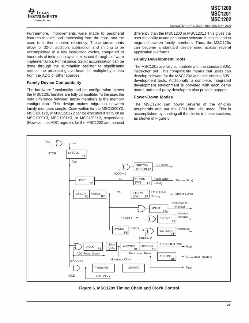
Power-Down Modes
The MSC120x can power several of the on-chipperipherals and put the CPU into Idle mode. This isaccomplished by shutting off the clocks to those sections,as shown in Figure 6.
(see Figure 9)
USECFB
MSECH
HMSECFE
MSINTFA
ACLKF6
divideby 64
MSECLFD FC
ms
µs
100ms
Flash Write
Timing
Flash Erase
Timing
WDTCON
SECINTF9
FF
ADCON0DC
FTCON[3:0]
FTCON[7:4]
EF
EF
secondsinterrupt
watchdog
fDATA
fSAMP
millisecondsinterrupt
ADC Output RateADCON3 ADCON2
DF DE
Decimation Ratio
SPICON/I2CCON 9A
C7
SCL/SCK
fCLK
(30µs to 40µs)
(5ms to 11ms)
PDCON.0
PDCON.1
Modulator Clock
PDCON.2
PDCON.3
IDLE CPU Clock
Timers 0/1
SYSCLK
ADC Power Down
USART0 fMOD
fSYS
STOP
fOSC
Figure 6. MSC120x Timing Chain and Clock Control
#$#$#$$SBAS317E − APRIL 2004 − REVISED MAY 2006
www.ti.com
22
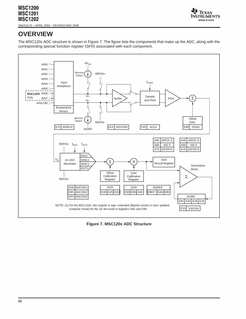
OVERVIEWThe MSC120x ADC structure is shown in Figure 7. The figure lists the components that make up the ADC, along with thecorresponding special function register (SFR) associated with each component.
Σ
Σ X
InputMultiplexer
MSC1200Only
TemperatureSensor
Buffer PGASample
and Hold
ADMUXD7h
REFIN+
REFIN−
REFIN+ fMOD
REFIN−
ADCON1DDh
ADCON2DEh
ADCON3DFh
AIPOL.5A4h
AIE.5A6h
OCR GCR ADRES
SUMR
D3h D2h D1h D6h D5h D4h DBh(1) DAh D9h
E5h E4h E3h E2h
OffsetCalibrationRegister
ADCON0DCh ACLKF6h
SSCONE1h
ODACE6h
OffsetDAC
∆Σ ADCModulator
FAST
SINC2SINC3
AUTO
ADCResult Register
Σ
SummationBlock
VIN
AIN0
AIN1
AIN2
AIN3
AIN4
AIN5
AIN6
AIN7
AINCOM
fSAMP
fDATA
GainCalibrationRegister
BurnoutDetect
AVDD
In+
AGND
In−
BurnoutDetect
NOTE: (1) For the MSC1202, this register is sign−extended (Bipolar mode) or zero−padded(Unipolar mode) for the 16−bit result in registers DAh and D9h.
AIPOL.6A4h
AIE.6A6h
AISTAT.5A7h AISTAT.6A7h
Figure 7. MSC120x ADC Structure
#$#$#$$
SBAS317E − APRIL 2004 − REVISED MAY 2006
www.ti.com
23
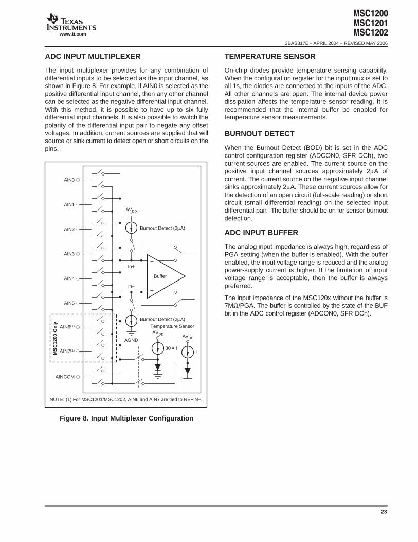
ADC INPUT MULTIPLEXER
The input multiplexer provides for any combination ofdifferential inputs to be selected as the input channel, asshown in Figure 8. For example, if AIN0 is selected as thepositive differential input channel, then any other channelcan be selected as the negative differential input channel.With this method, it is possible to have up to six fullydifferential input channels. It is also possible to switch thepolarity of the differential input pair to negate any offsetvoltages. In addition, current sources are supplied that willsource or sink current to detect open or short circuits on thepins.
AIN3
AIN4
AIN5
AIN0
AIN1
AIN2
AINCOM
NOTE: (1) For MSC1201/MSC1202, AIN6 and AIN7 are tied to REFIN−.
MS
C12
00O
nly
Burnout Detect (2µA)
Burnout Detect (2µA)
AGND
Buffer
Temperature Sensor
I80 • I
AVDD
AVDD AVDD
In+
In−
AIN6(1)
AIN7(1)
Figure 8. Input Multiplexer Configuration
TEMPERATURE SENSOR
On-chip diodes provide temperature sensing capability.When the configuration register for the input mux is set toall 1s, the diodes are connected to the inputs of the ADC.All other channels are open. The internal device powerdissipation affects the temperature sensor reading. It isrecommended that the internal buffer be enabled fortemperature sensor measurements.
BURNOUT DETECT
When the Burnout Detect (BOD) bit is set in the ADCcontrol configuration register (ADCON0, SFR DCh), twocurrent sources are enabled. The current source on thepositive input channel sources approximately 2µA ofcurrent. The current source on the negative input channelsinks approximately 2µA. These current sources allow forthe detection of an open circuit (full-scale reading) or shortcircuit (small differential reading) on the selected inputdifferential pair. The buffer should be on for sensor burnoutdetection.
ADC INPUT BUFFER
The analog input impedance is always high, regardless ofPGA setting (when the buffer is enabled). With the bufferenabled, the input voltage range is reduced and the analogpower-supply current is higher. If the limitation of inputvoltage range is acceptable, then the buffer is alwayspreferred.
The input impedance of the MSC120x without the buffer is7MΩ/PGA. The buffer is controlled by the state of the BUFbit in the ADC control register (ADCON0, SFR DCh).
#$#$#$$SBAS317E − APRIL 2004 − REVISED MAY 2006
www.ti.com
24
ADC ANALOG INPUT
When the buffer is not selected, the input impedance of theanalog input changes with ACLK clock frequency (ACLK,SFR F6h) and gain (PGA). The relationship is:
Impedance () 1fSAMP CS
AIN Impedance () 1MHzACLK Frequency
7M
PGA
where ACLK frequency (fACLK) fCLK
ACLK 1
and fMOD fACLK
64.
NOTE: The input impedance for PGA = 128 is the same asthat for PGA = 64 (that is, 7MΩ/64).
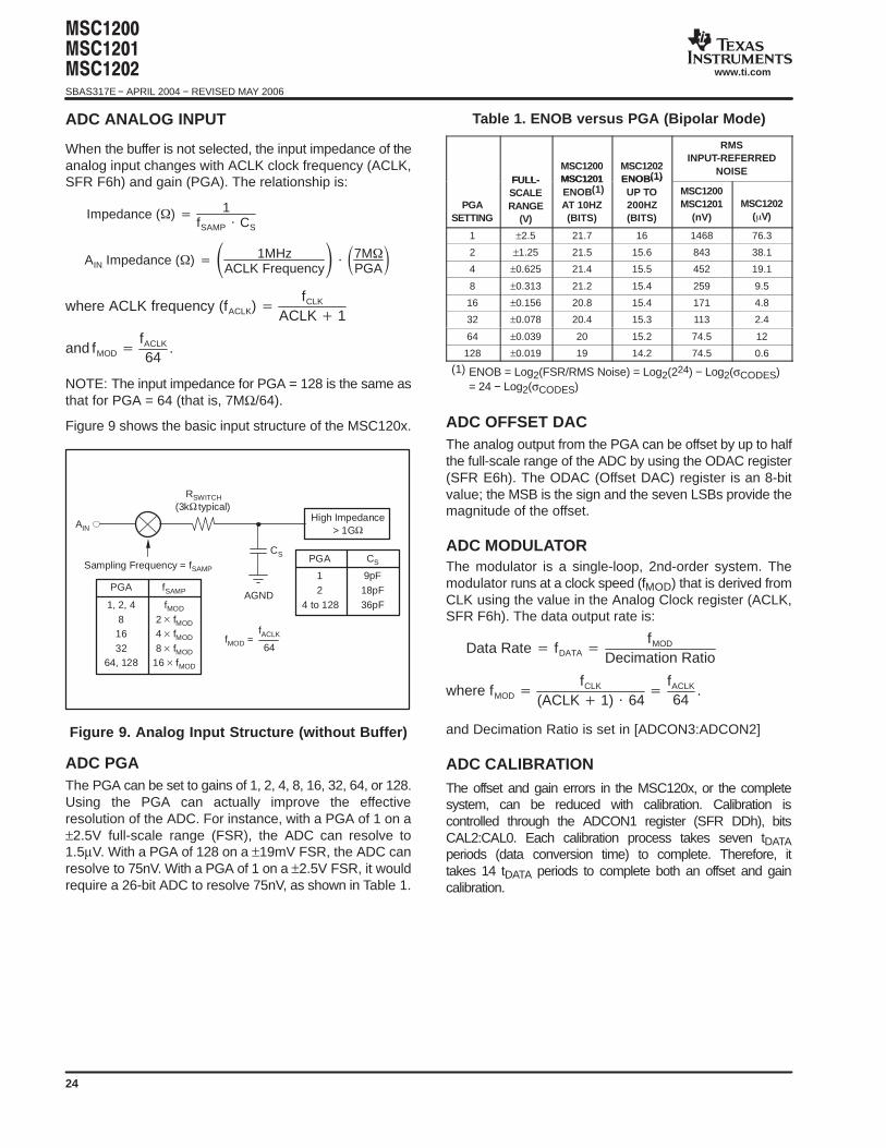
Figure 9 shows the basic input structure of the MSC120x.
RSWITCH(3kΩ typical)
Sampling Frequency = fSAMP
High Impedance> 1GΩ
CS
AGND
AIN
PGA fSAMP
1, 2, 4 fMOD
8 2 × fMOD
16 4 × fMOD
32 8 × fMOD
64, 128 16 × fMOD
PGA CS
1 9pF2 18pF
4 to 128 36pF
fMOD =fACLK
64
Figure 9. Analog Input Structure (without Buffer)
ADC PGAThe PGA can be set to gains of 1, 2, 4, 8, 16, 32, 64, or 128.Using the PGA can actually improve the effectiveresolution of the ADC. For instance, with a PGA of 1 on a±2.5V full-scale range (FSR), the ADC can resolve to1.5µV. With a PGA of 128 on a ±19mV FSR, the ADC canresolve to 75nV. With a PGA of 1 on a ±2.5V FSR, it wouldrequire a 26-bit ADC to resolve 75nV, as shown in Table 1.
Table 1. ENOB versus PGA (Bipolar Mode)
FULL-MSC1200MSC1201
MSC1202ENOB(1)
RMSINPUT-REFERRED
NOISE
PGASETTING
FULL-SCALERANGE
(V)
MSC1201 ENOB(1)
AT 10HZ(BITS)
ENOB(1)
UP TO200HZ(BITS)
MSC1200MSC1201
(nV)MSC1202
(V)
1 ±2.5 21.7 16 1468 76.3
2 ±1.25 21.5 15.6 843 38.1
4 ±0.625 21.4 15.5 452 19.1
8 ±0.313 21.2 15.4 259 9.5
16 ±0.156 20.8 15.4 171 4.8
32 ±0.078 20.4 15.3 113 2.4
64 ±0.039 20 15.2 74.5 12
128 ±0.019 19 14.2 74.5 0.6
(1) ENOB = Log2(FSR/RMS Noise) = Log2(224) − Log2(σCODES)= 24 − Log2(σCODES)
ADC OFFSET DACThe analog output from the PGA can be offset by up to halfthe full-scale range of the ADC by using the ODAC register(SFR E6h). The ODAC (Offset DAC) register is an 8-bitvalue; the MSB is the sign and the seven LSBs provide themagnitude of the offset.
ADC MODULATORThe modulator is a single-loop, 2nd-order system. Themodulator runs at a clock speed (fMOD) that is derived fromCLK using the value in the Analog Clock register (ACLK,SFR F6h). The data output rate is:
Data Rate fDATA fMOD
Decimation Ratio
where fMOD fCLK
(ACLK 1) 64
fACLK
64.
and Decimation Ratio is set in [ADCON3:ADCON2]
ADC CALIBRATIONThe offset and gain errors in the MSC120x, or the completesystem, can be reduced with calibration. Calibration iscontrolled through the ADCON1 register (SFR DDh), bitsCAL2:CAL0. Each calibration process takes seven tDATAperiods (data conversion time) to complete. Therefore, ittakes 14 tDATA periods to complete both an offset and gaincalibration.
#$#$#$$
SBAS317E − APRIL 2004 − REVISED MAY 2006
www.ti.com
25
For system calibration, the appropriate signal must beapplied to the inputs. It then computes an offset that willnullify offset in the system. The system gain calibrationrequires a positive full-scale differential input signal. It thencomputes a gain value to nullify gain errors in the system.Each of these calibrations will take seven tDATA periods tocomplete.
Calibration should be performed after power on. It shouldalso be done after a change in temperature, decimationratio, buffer, power supply, voltage reference, or PGA. Theoffset DAC will affect offset calibration; therefore, the valueof the offset should be zero before performing a calibration.
At the completion of calibration, the ADC Interrupt bit goeshigh, which indicates the calibration is finished and validdata is available.
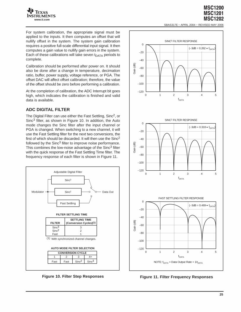
ADC DIGITAL FILTERThe Digital Filter can use either the Fast Settling, Sinc2, orSinc3 filter, as shown in Figure 10. In addition, the Automode changes the Sinc filter after the input channel orPGA is changed. When switching to a new channel, it willuse the Fast Settling filter for the next two conversions, thefirst of which should be discarded. It will then use the Sinc2
followed by the Sinc3 filter to improve noise performance.This combines the low-noise advantage of the Sinc3 filterwith the quick response of the Fast Settling Time filter. Thefrequency response of each filter is shown in Figure 11.
1
Fast
FILTERSETTLING TIME
(Conversion Cycles) (1)
Sinc3
Sinc2
Fast
321
(1) With synchronized channel changes.
CONVERSION CYCLE
AUTO MODE FILTER SELECTION
FILTER SETTLING TIME
Adjustable Digital Filter
Data OutModulator
Fast Settling
Sinc2
Sinc3
2
Fast
3
Sinc2
4+
Sinc3
Figure 10. Filter Step Responses
SINC3 FILTER RESPONSE
fDATA
0
−20
−40
−60
−80
−100
−1200 1 2 3 4 5
0 1 2 3 4 5
0 1 2 3 4 5
Gai
n(d
B)
SINC2 FILTER RESPONSE
fDATA
0
−20
−40
−60
−80
−100
−120
Gai
n(d
B)
FAST SETTLING FILTER RESPONSE
fDATA
0
−20
−40
−60
−80
−100
−120
NOTE: fDATA = Data Output Rate = 1/tDATA
Gai
n(d
B)
(−3dB = 0.318 • fDATA)
(−3dB = 0.469 • fDATA)
(−3dB = 0.262 • fDATA)
Figure 11. Filter Frequency Responses
#$#$#$$SBAS317E − APRIL 2004 − REVISED MAY 2006
www.ti.com
26
VOLTAGE REFERENCE
The MSC120x can use either an internal or externalvoltage reference. The voltage reference selection iscontrolled via ADC Control Register 0 (ADCON0, SFRDCh). The default power-up configuration for the voltagereference is 2.5V internal.
The internal voltage reference can be selected as either1.25V or 2.5V. The analog power supply (AVDD) must bewithin the specified range for the selected internal voltagereference. The valid ranges are: VREF = 2.5 internal(AVDD = 3.3V to 5.25V) and VREF = 1.25 internal(AVDD = 2.7V to 5.25V). If the internal VREF is selected,then AGND must be connected to REFIN−. TheREFOUT/REFIN+ pin should also have a 0.1µF capacitorconnected to AGND as close as possible to the pin. If theinternal VREF is not used, then VREF should be disabled inADCON0.
If the external voltage reference is selected, it can be usedas either a single-ended input or differential input, forratiometric measures. When using an external reference,it is important to note that the input current will increase forVREF with higher PGA settings and with a higher modulatorfrequency. The external voltage reference can be usedover the input range specified in the ElectricalCharacteristics section.
IDAC
The 8-bit IDAC in the MSC120x provides a current sourcethat can be used for ratiometric measurements. The IDACoperates from its own voltage reference and is notdependent on the ADC voltage reference. The full-scaleoutput current of the IDAC is approximately 1mA (withinthe compliance voltage range). The equation for the IDACoutput current is:
IDACOUT A IDAC 3.9A (at 25C)
The IDAC output voltage cannot exceed the compliancevoltage of AVDD − 1.5V.
RESET
The MSC120x can be reset from the following sources:
Power-on reset
External reset
Software reset
Watchdog timer reset
Brownout reset
An external reset is accomplished by taking the RST pinhigh for two tOSC periods, followed by taking the RST pinlow. A software reset is accomplished through the SystemReset register (SRTST, 0F7h). A watchdog timer reset isenabled and controlled through Hardware ConfigurationRegister 0 (HCR0) and the Watchdog Timer register(WDTCON, 0FFh). A brownout reset is enabled throughHardware Configuration Register 1 (HCR1). Power-onreset and external reset complete after 217 clock cycles,using the internal oscillator in low-frequency mode.Brownout reset, watchdog timer reset, and software resetcomplete after 215 clock cycles, using the active clocksource.
All sources of reset cause the digital pins to be pulled highfrom the initiation of the reset procedure. For an externalreset, taking the RST pin high stops device operation(crystal oscillation, internal oscillator, or PLL circuitoperation) and causes all digital pins to be pulled high fromthat point. Taking the RST pin low initiates the resetprocedure.
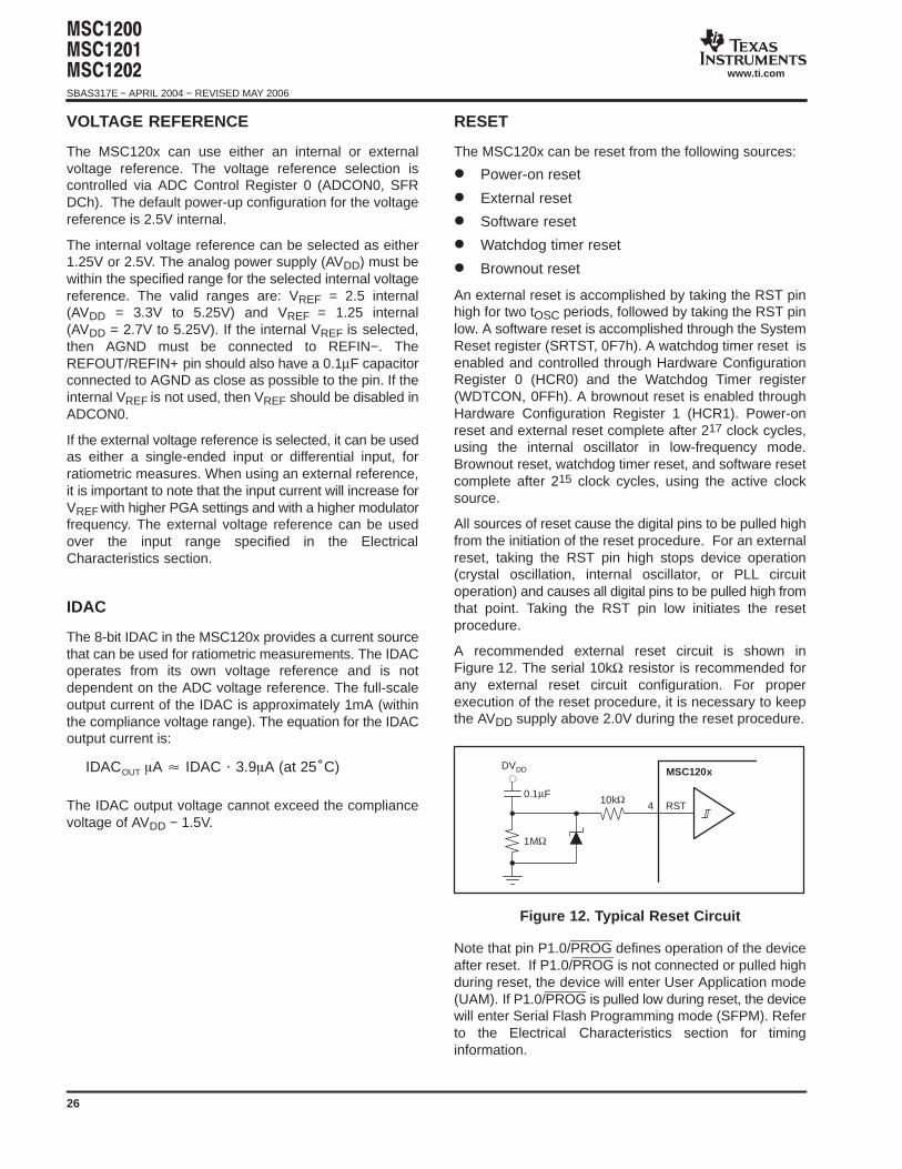
A recommended external reset circuit is shown inFigure 12. The serial 10kΩ resistor is recommended forany external reset circuit configuration. For properexecution of the reset procedure, it is necessary to keepthe AVDD supply above 2.0V during the reset procedure.
10kΩ4 RST
MSC120x
0.1µF
1MΩ
DVDD
Figure 12. Typical Reset Circuit
Note that pin P1.0/PROG defines operation of the deviceafter reset. If P1.0/PROG is not connected or pulled highduring reset, the device will enter User Application mode(UAM). If P1.0/PROG is pulled low during reset, the devicewill enter Serial Flash Programming mode (SFPM). Referto the Electrical Characteristics section for timinginformation.
#$#$#$$
SBAS317E − APRIL 2004 − REVISED MAY 2006
www.ti.com
27
POWER ON RESET
The on-chip Power On Reset (POR) circuitry releases thedevice from reset when DVDD ≈ 2.0V. The power supplyramp rate does not affect the POR. If the power supply fallsbelow 1.0V for longer than 200ms, the POR will execute.If the power supply falls below 1.0V for less than 200ms,unexpected operation may occur. If these conditions arenot met, the POR will not execute. For example, a negativespike on the DVDD supply that does not remain below 1.0Vfor at least 200ms, will not initiate a POR.
If the Digital Brownout Reset circuit is on, the POR circuithas no effect.
DIGITAL BROWNOUT RESET
The Digital Brownout Reset (DBOR) is enabled throughHCR1. If the conditions for proper POR are not met, theDBOR can be used to ensure proper device operation. TheDBOR will hold the state of the device when the powersupply drops below the threshold level programmed inHCR1, and then generate a reset when the supply risesabove the threshold level. Note that as the device isreleased from reset and program execution begins, thedevice current consumption may increase, which canresult in a power supply voltage drop, which may initiateanother brownout condition. Also, the DBOR comparisonis done against an analog reference; therefore, AVDD mustbe within its valid operating range for DBOR to function.
The DBOR level should be chosen to match closely withthe application. That is, with a high external clockfrequency, the DBOR level should match the minimumoperating voltage range for the device or improperoperation may still occur.
ANALOG LOW-VOLTAGE DETECT
The MSC120x contain an analog low-voltage detectcircuit. When the analog supply drops below the valueprogrammed in LVDCON (SFR E7h), an interrupt isgenerated, and/or the flag is set.
IDLE MODE
Idle mode is entered by setting the IDLE bit in the PowerControl register (PCON, 087h). In Idle mode, the CPU,Timer0, Timer1, and USART are stopped, but all otherperipherals and digital pins remain active. The device canbe returned to active mode via an active internal or externalinterrupt. This mode is typically used for reducing powerconsumption between ADC samples.
By configuring the device prior to entering Idle mode,further power reductions can be achieved (while in Idlemode). These power reductions include powering downperipherals not in use in the PDCON register (0F1h), andreducing the system clock frequency by using the SystemClock Divider register (SYSCLK, 0C7h).
STOP MODE
Stop mode is entered by setting the STOP bit in the PowerControl register (PCON, 087h). In Stop mode, all internalclocks are halted. This mode has the lowest powerconsumption. The device can be returned to active modeonly via an external reset or power-on reset (not abrownout reset).
By configuring the device prior to entering Stop mode,further power reductions can be achieved (while in Stopmode). These power reductions include halting theexternal clock into the device, configuring all digital I/Opins as open drain with low output drive, disabling the ADCbuffer, disabling the internal VREF, and setting PDCON to0FFh to power down all peripherals.
In Stop mode, all digital pins retain their values.
POWER CONSUMPTION CONSIDERATIONS
The following suggestions will reduce currentconsumption in the MSC120x devices:
1. Use the lowest supply voltage that will work in theapplication for both AVDD and DVDD.
2. Use the lowest clock frequency that will work in theapplication.
3. Use Idle mode and the system clock dividerwhenever possible. Note that the system clockdivider also affects the ADC clock.
4. Avoid using 8051-compatible I/O mode on the I/Oports. The internal pull-up resistors will draw currentwhen the outputs are low.
5. Use the delay line for Flash Memory control bysetting the FRCM bit in the FMCON register (SFREEh).
6. Power down the internal oscillator in External Clockmode by setting the PDICLK bit in the PDCONregister (SFR F1h).
7. Power down peripherals when they are not needed.Refer to SFR PDCON, LVDCON, ADCON0, andIDAC.
#$#$#$$SBAS317E − APRIL 2004 − REVISED MAY 2006
www.ti.com
28
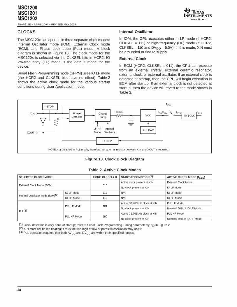
CLOCKS
The MSC120x can operate in three separate clock modes:Internal Oscillator mode (IOM), External Clock mode(ECM), and Phase Lock Loop (PLL) mode. A blockdiagram is shown in Figure 13. The clock mode for theMSC120x is selected via the CLKSEL bits in HCR2. IOlow-frequency (LF) mode is the default mode for thedevice.
Serial Flash Programming mode (SFPM) uses IO LF mode(the HCR2 and CLKSEL bits have no effect). Table 2shows the active clock mode for the various startupconditions during User Application mode.
Internal Oscillator
In IOM, the CPU executes either in LF mode (if HCR2,CLKSEL = 111) or high-frequency (HF) mode (if HCR2,CLKSEL = 110 and DVDD = 5.0V). In this mode, XIN mustbe grounded or tied to supply.
External Clock
In ECM (HCR2, CLKSEL = 011), the CPU can executefrom an external crystal, external ceramic resonator,external clock, or external oscillator. If an external clock isdetected at startup, then the CPU will begin execution inECM after startup. If an external clock is not detected atstartup, then the device will revert to the mode shown inTable 2.
100kΩ
InternalOscillator
LF/HFMode
STOP
PhaseDetector
XIN
XOUT
ChargePump
VCO
PLL DAC
PLLDIV
SYSCLK
tOSC
(1)
NOTE: (1) Disabled in PLL mode; therefore, an external resistor between XIN and XOUT is required.
tPLL/tIOM tSYS tCLK
Figure 13. Clock Block Diagram
Table 2. Active Clock Modes
SELECTED CLOCK MODE HCR2, CLKSEL2:0 STARTUP CONDITION(1) ACTIVE CLOCK MODE (f SYS)
External Clock Mode (ECM) 010Active clock present at XIN External Clock Mode
External Clock Mode (ECM) 010No clock present at XIN IO LF Mode
Internal Oscillator Mode (IOM)(2)IO LF Mode 111 N/A IO LF Mode
Internal Oscillator Mode (IOM)(2)IO HF Mode 110 N/A IO HF Mode
PLL LF Mode 101Active 32.768kHz clock at XIN PLL LF Mode
PLL(3)
PLL LF Mode 101No clock present at XIN Nominal 50% of IO LF Mode
PLL(3)
PLL HF Mode 100Active 32.768kHz clock at XIN PLL HF Mode
PLL HF Mode 100No clock present at XIN Nominal 50% of IO HF Mode
(1) Clock detection is only done at startup; refer to Serial Flash Programming Timing parameter tRFD in Figure 2.(2) XIN must not be left floating; it must be tied high or low or parasitic oscillation may occur.(3) PLL operation requires that both AVDD and DVDD are within their specified ranges.
#$#$#$$
SBAS317E − APRIL 2004 − REVISED MAY 2006
www.ti.com
29
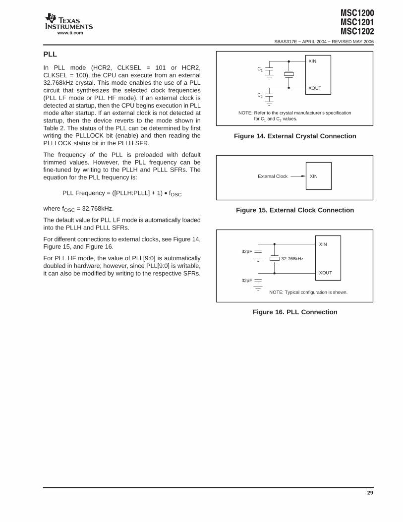
PLL
In PLL mode (HCR2, CLKSEL = 101 or HCR2,CLKSEL = 100), the CPU can execute from an external32.768kHz crystal. This mode enables the use of a PLLcircuit that synthesizes the selected clock frequencies(PLL LF mode or PLL HF mode). If an external clock isdetected at startup, then the CPU begins execution in PLLmode after startup. If an external clock is not detected atstartup, then the device reverts to the mode shown inTable 2. The status of the PLL can be determined by firstwriting the PLLLOCK bit (enable) and then reading thePLLLOCK status bit in the PLLH SFR.
The frequency of the PLL is preloaded with defaulttrimmed values. However, the PLL frequency can befine-tuned by writing to the PLLH and PLLL SFRs. Theequation for the PLL frequency is:
PLL Frequency = ([PLLH:PLLL] + 1) • fOSC
where fOSC = 32.768kHz.
The default value for PLL LF mode is automatically loadedinto the PLLH and PLLL SFRs.
For different connections to external clocks, see Figure 14,Figure 15, and Figure 16.
For PLL HF mode, the value of PLL[9:0] is automaticallydoubled in hardware; however, since PLL[9:0] is writable,it can also be modified by writing to the respective SFRs.
XIN
XOUT
C1
C2
Refer to the crystal manufacturer’s specificationfor C1 and C2 values.
NOTE:
Figure 14. External Crystal Connection
XINExternal Clock
Figure 15. External Clock Connection
XOUT
XIN
32pF
32pF
32.768kHz
NOTE: Typical configuration is shown.
Figure 16. PLL Connection
#$#$#$$SBAS317E − APRIL 2004 − REVISED MAY 2006
www.ti.com
30
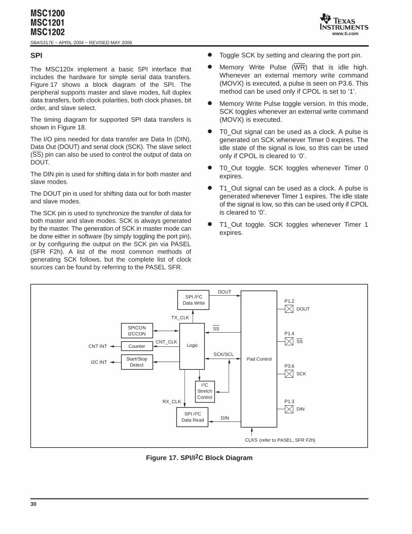
SPI
The MSC120x implement a basic SPI interface thatincludes the hardware for simple serial data transfers.Figure 17 shows a block diagram of the SPI. Theperipheral supports master and slave modes, full duplexdata transfers, both clock polarities, both clock phases, bitorder, and slave select.
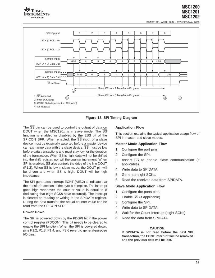
The timing diagram for supported SPI data transfers isshown in Figure 18.
The I/O pins needed for data transfer are Data In (DIN),Data Out (DOUT) and serial clock (SCK). The slave select(SS) pin can also be used to control the output of data onDOUT.
The DIN pin is used for shifting data in for both master andslave modes.
The DOUT pin is used for shifting data out for both masterand slave modes.
The SCK pin is used to synchronize the transfer of data forboth master and slave modes. SCK is always generatedby the master. The generation of SCK in master mode canbe done either in software (by simply toggling the port pin),or by configuring the output on the SCK pin via PASEL(SFR F2h). A list of the most common methods ofgenerating SCK follows, but the complete list of clocksources can be found by referring to the PASEL SFR.
Toggle SCK by setting and clearing the port pin.
Memory Write Pulse (WR) that is idle high.Whenever an external memory write command(MOVX) is executed, a pulse is seen on P3.6. Thismethod can be used only if CPOL is set to ‘1’.
Memory Write Pulse toggle version. In this mode,SCK toggles whenever an external write command(MOVX) is executed.
T0_Out signal can be used as a clock. A pulse isgenerated on SCK whenever Timer 0 expires. Theidle state of the signal is low, so this can be usedonly if CPOL is cleared to ‘0’.
T0_Out toggle. SCK toggles whenever Timer 0expires.
T1_Out signal can be used as a clock. A pulse isgenerated whenever Timer 1 expires. The idle stateof the signal is low, so this can be used only if CPOLis cleared to ‘0’.
T1_Out toggle. SCK toggles whenever Timer 1expires.
SPI /I2CData Write
SPICONI2CCON
I2CStretchControl
Counter
Start/StopDetect
SPI /I2CData Read
Pad Control
DOUT
P1.2
P1.4
P3.6
P1.3
Logic
DOUT
TX_CLK
RX_CLK
SS
SCK/SCL
CNT_CLKCNT INT
I2C INT
DIN
CLKS (refer to PASEL, SFR F2h)
SS
SCK
DIN
Figure 17. SPI/I 2C Block Diagram
#$#$#$$
SBAS317E − APRIL 2004 − REVISED MAY 2006
www.ti.com
31
1) SS Asserted2) First SCK Edge3) CNTIF Set (dependent on CPHA bit)4) SS Negated
SCK Cycle #
MSB 6 5 4 3 2 1 LSB
MSB 6 5 4 3 2 1 LSB
Slave CPHA = 0 Transfer in Progress
2
431
1 2 3 4 5 6 7 8
Slave CPHA = 1 Transfer in Progress
Sample Input
(CPHA = 0) Data Out
(CPHA = 1) Data Out
Sample Input
SS to Slave
SCK (CPOL = 0)
SCK (CPOL = 1)
Figure 18. SPI Timing Diagram
The SS pin can be used to control the output of data onDOUT when the MSC120x is in slave mode. The SSfunction is enabled or disabled by the ESS bit of theSPICON SFR. When enabled, the SS input of a slavedevice must be externally asserted before a master devicecan exchange data with the slave device. SS must be lowbefore data transactions and must stay low for the durationof the transaction. When SS is high, data will not be shiftedinto the shift register, nor will the counter increment. WhenSPI is enabled, SS also controls the drive of the line DOUT(P1.2). When SS is low in slave mode, the DOUT pin willbe driven and when SS is high, DOUT will be highimpedance.
The SPI generates interrupt ECNT (AIE.2) to indicate thatthe transfer/reception of the byte is complete. The interruptgoes high whenever the counter value is equal to 8(indicating that eight SCKs have occurred). The interruptis cleared on reading or writing to the SPIDATA register.During the data transfer, the actual counter value can beread from the SPICON SFR.
Power Down
The SPI is powered down by the PDSPI bit in the powercontrol register (PDCON). This bit needs to be cleared toenable the SPI function. When the SPI is powered down,pins P1.2, P1.3, P1.4, and P3.6 revert to general-purposeI/O pins.
Application Flow
This section explains the typical application usage flow ofSPI in master and slave modes.
Master Mode Application Flow
1. Configure the port pins.
2. Configure the SPI.
3. Assert SS to enable slave communication (ifapplicable).
4. Write data to SPIDATA.
5. Generate eight SCKs.
6. Read the received data from SPIDATA.
Slave Mode Application Flow
1. Configure the ports pins.
2. Enable SS (if applicable).
3. Configure the SPI.
4. Write data to SPIDATA.
5. Wait for the Count Interrupt (eight SCKs).
6. Read the data from SPIDATA.
CAUTION:If SPIDATA is not read before the next SPItransaction, the ECNT interrupt will be removedand the previous data will be lost.
#$#$#$$SBAS317E − APRIL 2004 − REVISED MAY 2006
www.ti.com
32
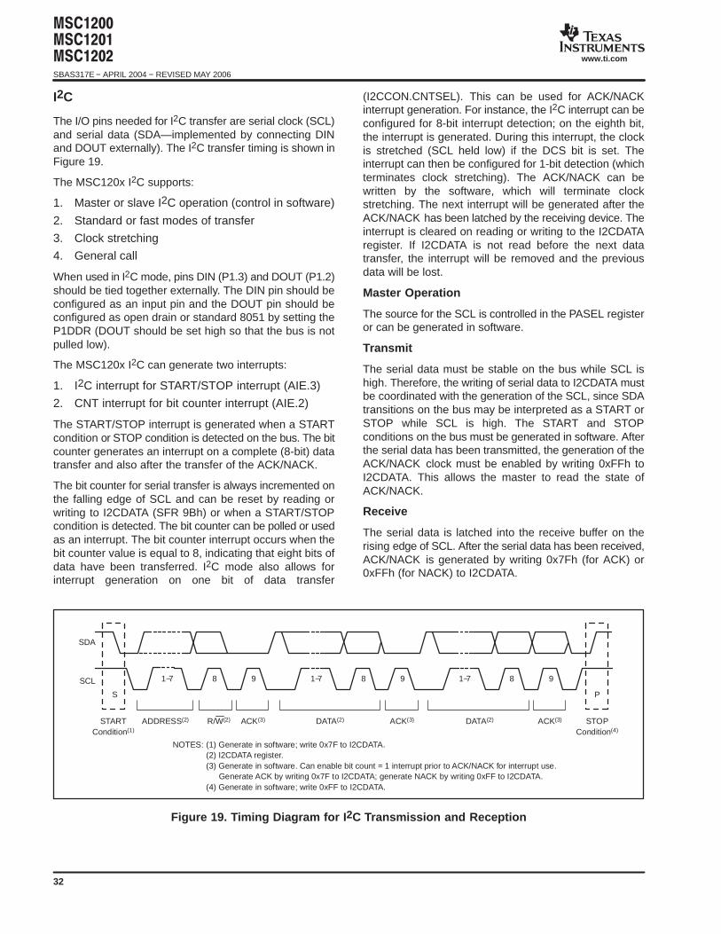
I2C
The I/O pins needed for I2C transfer are serial clock (SCL)and serial data (SDA—implemented by connecting DINand DOUT externally). The I2C transfer timing is shown inFigure 19.
The MSC120x I2C supports:
1. Master or slave I2C operation (control in software)
2. Standard or fast modes of transfer
3. Clock stretching
4. General call
When used in I2C mode, pins DIN (P1.3) and DOUT (P1.2)should be tied together externally. The DIN pin should beconfigured as an input pin and the DOUT pin should beconfigured as open drain or standard 8051 by setting theP1DDR (DOUT should be set high so that the bus is notpulled low).
The MSC120x I2C can generate two interrupts:
1. I2C interrupt for START/STOP interrupt (AIE.3)
2. CNT interrupt for bit counter interrupt (AIE.2)
The START/STOP interrupt is generated when a STARTcondition or STOP condition is detected on the bus. The bitcounter generates an interrupt on a complete (8-bit) datatransfer and also after the transfer of the ACK/NACK.
The bit counter for serial transfer is always incremented onthe falling edge of SCL and can be reset by reading orwriting to I2CDATA (SFR 9Bh) or when a START/STOPcondition is detected. The bit counter can be polled or usedas an interrupt. The bit counter interrupt occurs when thebit counter value is equal to 8, indicating that eight bits ofdata have been transferred. I2C mode also allows forinterrupt generation on one bit of data transfer
(I2CCON.CNTSEL). This can be used for ACK/NACKinterrupt generation. For instance, the I2C interrupt can beconfigured for 8-bit interrupt detection; on the eighth bit,the interrupt is generated. During this interrupt, the clockis stretched (SCL held low) if the DCS bit is set. Theinterrupt can then be configured for 1-bit detection (whichterminates clock stretching). The ACK/NACK can bewritten by the software, which will terminate clockstretching. The next interrupt will be generated after theACK/NACK has been latched by the receiving device. Theinterrupt is cleared on reading or writing to the I2CDATAregister. If I2CDATA is not read before the next datatransfer, the interrupt will be removed and the previousdata will be lost.
Master Operation
The source for the SCL is controlled in the PASEL registeror can be generated in software.
Transmit
The serial data must be stable on the bus while SCL ishigh. Therefore, the writing of serial data to I2CDATA mustbe coordinated with the generation of the SCL, since SDAtransitions on the bus may be interpreted as a START orSTOP while SCL is high. The START and STOPconditions on the bus must be generated in software. Afterthe serial data has been transmitted, the generation of theACK/NACK clock must be enabled by writing 0xFFh toI2CDATA. This allows the master to read the state ofACK/NACK.
Receive
The serial data is latched into the receive buffer on therising edge of SCL. After the serial data has been received,ACK/NACK is generated by writing 0x7Fh (for ACK) or0xFFh (for NACK) to I2CDATA.
SDA
SCL 1−7 8
PS
STOPCondition(4)
STARTCondition(1)
ACK(3)ACK(3)ACK(3)R/W(2) DATA(2)DATA(2)ADDRESS(2)
9 1−7 8 9 1−7 8 9
(1) Generate in software; write 0x7F to I2CDATA.(2) I2CDATA register.(3) Generate in software. Can enable bit count = 1 interrupt prior to ACK/NACK for interrupt use.
Generate ACK by writing 0x7F to I2CDATA; generate NACK by writing 0xFF to I2CDATA.(4) Generate in software; write 0xFF to I2CDATA.
NOTES:
Figure 19. Timing Diagram for I 2C Transmission and Reception
#$#$#$$
SBAS317E − APRIL 2004 − REVISED MAY 2006
www.ti.com
33
Slave Operation
Slave operation is supported, but address recognition,R/W determination, and ACK/NACK must be done undersoftware control. The Disable Clock Stretch (DCS) bit canbe set to disable clock stretching. When the DCS bit is set,the device will no longer stretch the clock and will notgenerate interrupts. This bit can be used to disable clockstretch interrupts when there is no address match. This bitis automatically cleared when a start or repeated startcondition occurs.
Transmit
Once address recognition, R/W determination, andACK/NACK are complete, the serial data to be transferredcan be written to I2CDATA. The data is automaticallyshifted out based on the master SCL. After datatransmission, CNTIF is generated and SCL is stretched bythe MSC120x until the I2CDATA register is written with a0xFFh. The ACK/NACK from the master can then be read.
Receive
Once address recognition, R/W determination, andACK/NACK are complete, I2CDATA must be written with0xFFh to enable data reception. Upon completion of thedata shift, the MSC120x generates the CNT interrupt andstretches SCL. Received data can then be read fromI2CDATA. After the serial data has been received,ACK/NACK is generated by writing 0x7Fh (for ACK) or0xFFh (for NACK) to I2CDATA. The write to I2CDATAclears the CNT interrupt and clock stretch.
MEMORY MAP
The MSC120x contain on-chip SFR, Flash Memory,Configuration Memory, Scratchpad SRAM Memory, andBoot ROM. The SFR registers are primarily used forcontrol and status. The standard 8051 features andadditional peripheral features of the MSC120x arecontrolled through the SFR. Reading from an undefinedSFR returns zero. Writing to undefined SFR registers is notrecommended and will have indeterminate effects.
Flash Memory is used for both Program Memory and DataMemory; however, program execution can only occur fromProgram Memory. Program/Data Memory partition size isselectable. The partition size is set through HCR0 (in theConfiguration Memory), which is programmed serially.Both Program and Data Flash Memory are erasable andwritable (programmable) in UAM. Erase and write timingof Flash Memory is controlled in the Flash Memory TimingControl register (FTCON, SFR 0EFh). As an added
precaution, a lock feature can be activated through HCR0,which disables erase/write operation to 4kB of ProgramFlash Memory or the entire Program Flash Memory inUAM.
FLASH MEMORY
The page size for Flash memory is 64 bytes. Therespective page must be erased before it can be written to,regardless of whether it is mapped to Program memory orData memory space. The MSC120x use a memoryaddressing scheme that separates Program Memory(FLASH/ROM) from Data Memory (FLASH/RAM).Addressing of program and data segments can overlapsince they are accessed by different instructions.
The MSC120x have three hardware configurationregisters (HCR0, HCR1, and HCR2) that areprogrammable only during Flash Memory Programmingmode.
The MSC120x allow the user to partition the Flash Memorybetween Program Memory and Data Memory. Forinstance, the MSC120xY3 contain 8kB of Flash Memoryon-chip. Through the hardware configuration registers, theuser can define the partition between Program Memory(PM) and Data Memory (DM), as shown in Table 3,Table 4, and Figure 20. The MSC120x families offer twomemory configurations.
Table 3. Flash Memory Partitioning
HCR0 MSC120xY2 MSC120xY3
DFSEL PM DM PM DM
00 2kB 2kB 4kB 4kB
01 2kB 2kB 6kB 2kB
10 3kB 1kB 7kB 1kB
11(default)
4kB 0kB 8kB 0kB
Table 4. Flash Memory Partitioning Addresses
HCR0 MSC120xY2 MSC120xY3
DFSEL PM DM PM DM
00 0000−07FF 0400−0BFF 0000−0FFF 0400−13FF
01 0000−07FF 0400−0BFF 0000−17FF 0400−0BFF
10 0000−0BFF 0400−07FF 0000−1BFF 0400−07FF
11(default)
0000−0FFF 0000 0000−1FFF 0000
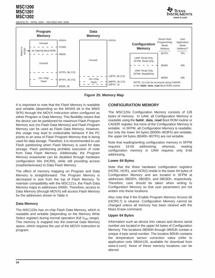
#$#$#$$SBAS317E − APRIL 2004 − REVISED MAY 2006
www.ti.com
34
UnusedUnused
Serial FlashProgramming
ModeAddress
UserApplication
ModeAddress(1)
Unused
1K Internal Boot ROM
Sel
ect
inH
CR
0
0000h, 0k
NOTE: (1) Can be accessed using CADDRor the faddr_data_read Boot ROM routine.
1FFFh, 8k (Y3)
0FFFh, 4k (Y2)
FC00h
F800h
FFFFh FFFFh
ProgramMemory
03FFh, 1k
13FFh, 5k (Y3)
0BFFh, 3k (Y2)
DataMemory
On−ChipFlash
On−ChipFlash
UAM: Read OnlySFPM: Read Only
UAM: Read OnlySFPM: Read/Write
807Fh
8000h
8040h
7Fh
00h
40h
ConfigurationMemory
Figure 20. Memory Map
It is important to note that the Flash Memory is readableand writable (depending on the MXWS bit in the MWSSFR) through the MOVX instruction when configured aseither Program or Data Memory. This flexibility means thatthe device can be partitioned for maximum Flash ProgramMemory size (no Flash Data Memory) and Flash ProgramMemory can be used as Flash Data Memory. However,this usage may lead to undesirable behavior if the PCpoints to an area of Flash Program Memory that is beingused for data storage. Therefore, it is recommended to useFlash partitioning when Flash Memory is used for datastorage. Flash partitioning prohibits execution of codefrom Data Flash Memory. Additionally, the ProgramMemory erase/write can be disabled through hardwareconfiguration bits (HCR0), while still providing access(read/write/erase) to Data Flash Memory.
The effect of memory mapping on Program and DataMemory is straightforward. The Program Memory isdecreased in size from the top of Flash Memory. Tomaintain compatibility with the MSC121x, the Flash DataMemory maps to addresses 0400h. Therefore, access toData Memory (through MOVX) will access Flash Memoryfor the addresses shown in Table 4.
Data Memory
The MSC120x has on-chip Flash Data Memory, which isreadable and writable (depending on the Memory WriteSelect register) during normal operation (full VDD range).This memory is mapped into the external Data Memoryspace, which requires the use of the MOVX instruction toprogram.
CONFIGURATION MEMORY
The MSC120x Configuration Memory consists of 128bytes of memory. In UAM, all Configuration Memory isreadable using the faddr_data_read Boot ROM routine orCADDR register, but none of the Configuration Memory iswritable. In SFPM, all Configuration Memory is readable,but only the lower 64 bytes (8000h−803Fh) are writable;the upper 64 bytes (8040h−807Fh) are not writable.
Note that reading/writing configuration memory in SFPMrequires 16-bit addressing; whereas, readingconfiguration memory in UAM requires only 8-bitaddressing.
Lower 64 Bytes
Note that the three hardware configuration registers(HCR0, HCR1, and HCR2) reside in the lower 64 bytes ofConfiguration Memory and are located in SFPM ataddresses 0803Fh, 0803Eh, and 0803Dh, respectively.Therefore, care should be taken when writing toConfiguration Memory so that user parameters are notwritten into these locations.
Also note that if the Enable Program Memory Access bit(HCR0.7) is cleared, Configuration Memory cannot bechanged unless all memory has been cleared with theMass Erase command.
Upper 64 Bytes
Information such as device trim values and device serialnumber are located in the upper 64 bytes of ConfigurationMemory. The locations 08050h through 08053h contain aunique 4-byte serial number. The location 8054h containsthe temperature sensor correction value (refer toapplication note SBAA126, available for download fromwww.ti.com). None of these memory locations can bealtered.
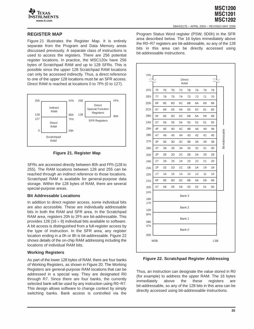
#$#$#$$
SBAS317E − APRIL 2004 − REVISED MAY 2006
www.ti.com
35
REGISTER MAPFigure 21 illustrates the Register Map. It is entirelyseparate from the Program and Data Memory areasdiscussed previously. A separate class of instructions isused to access the registers. There are 256 potentialregister locations. In practice, the MSC120x have 256bytes of Scratchpad RAM and up to 128 SFRs. This ispossible since the upper 128 Scratchpad RAM locationscan only be accessed indirectly. Thus, a direct referenceto one of the upper 128 locations must be an SFR access.Direct RAM is reached at locations 0 to 7Fh (0 to 127).
FFh 255
128
FFh
80h80h
7Fh
00h
IndirectRAM
DirectRAM
ScratchpadRAM
SFR Registers
DirectSpecial Function
Registers
255
128
127
0
Figure 21. Register Map
SFRs are accessed directly between 80h and FFh (128 to255). The RAM locations between 128 and 255 can bereached through an indirect reference to those locations.Scratchpad RAM is available for general-purpose datastorage. Within the 128 bytes of RAM, there are severalspecial-purpose areas.
Bit Addressable Locations
In addition to direct register access, some individual bitsare also accessible. These are individually addressablebits in both the RAM and SFR area. In the ScratchpadRAM area, registers 20h to 2Fh are bit-addressable. Thisprovides 128 (16 × 8) individual bits available to software.A bit access is distinguished from a full-register access bythe type of instruction. In the SFR area, any registerlocation ending in a 0h or 8h is bit-addressable. Figure 22shows details of the on-chip RAM addressing including thelocations of individual RAM bits.
Working Registers
As part of the lower 128 bytes of RAM, there are four banksof Working Registers, as shown in Figure 20. The WorkingRegisters are general-purpose RAM locations that can beaddressed in a special way. They are designated R0through R7. Since there are four banks, the currentlyselected bank will be used by any instruction using R0−R7.This design allows software to change context by simplyswitching banks. Bank access is controlled via the
Program Status Word register (PSW; 0D0h) in the SFRarea described below. The 16 bytes immediately abovethe R0−R7 registers are bit-addressable, so any of the 128bits in this area can be directly accessed usingbit-addressable instructions.
7Fh
2Fh 7F
77
6F
67
5F
57
4F
47
3F
37
2F
27
1F
17
0F
07
7E
76
6E
66
5E
56
4E
46
3E
36
2E
26
1E
16
0E
06
7D
75
6D
65
5D
55
4D
45
3D
35
2D
25
1D
15
0D
05
7C
74
6C
64
5C
54
4C
44
3C
34
2C
24
1C
14
0C
04
7B
73
6B
63
5B
53
4B
43
3B
33
2B
23
1B
13
0B
03
7A
72
6A
62
5A
52
4A
42
3A
32
2A
22
1A
12
0A
02
79
71
69
61
59
51
49
41
39
31
29
21
19
11
09
01
78
70
68
60
58
50
48
40
38
30
28
20
18
10
08
00
2Dh
2Eh
2Ch
2Bh
2Ah
29h
28h
27h
26h
25h
24h
23h
22h
21h
20h
1Fh
18h17h
10h
0Fh
08h07h
00h
DirectRAM
Bank 3
Bit-
Add
ress
able
Bank 2
Bank 1
Bank 0
MSB LSB
Figure 22. Scratchpad Register Addressing
Thus, an instruction can designate the value stored in R0(for example) to address the upper RAM. The 16 bytesimmediately above the these registers arebit-addressable, so any of the 128 bits in this area can bedirectly accessed using bit-addressable instructions.
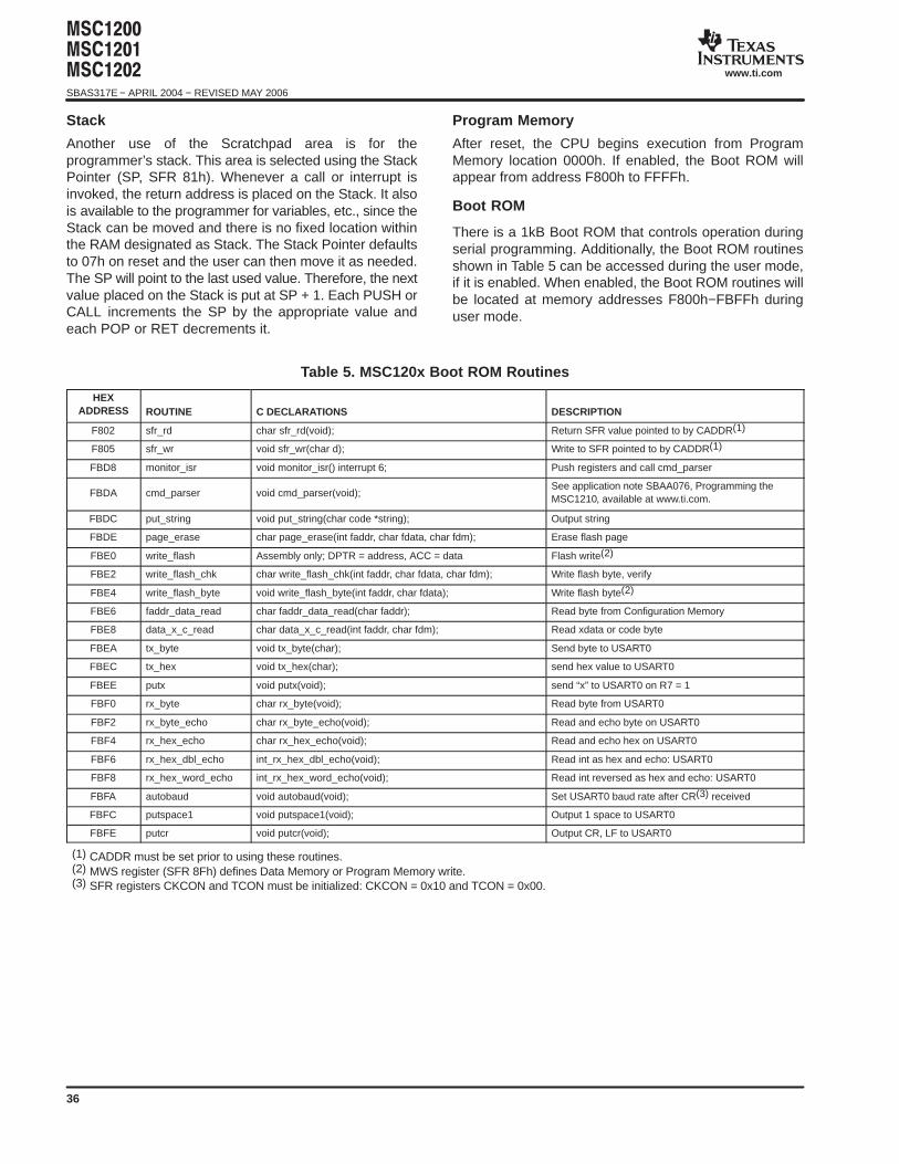
#$#$#$$SBAS317E − APRIL 2004 − REVISED MAY 2006
www.ti.com
36
Stack
Another use of the Scratchpad area is for theprogrammer’s stack. This area is selected using the StackPointer (SP, SFR 81h). Whenever a call or interrupt isinvoked, the return address is placed on the Stack. It alsois available to the programmer for variables, etc., since theStack can be moved and there is no fixed location withinthe RAM designated as Stack. The Stack Pointer defaultsto 07h on reset and the user can then move it as needed.The SP will point to the last used value. Therefore, the nextvalue placed on the Stack is put at SP + 1. Each PUSH orCALL increments the SP by the appropriate value andeach POP or RET decrements it.
Program Memory
After reset, the CPU begins execution from ProgramMemory location 0000h. If enabled, the Boot ROM willappear from address F800h to FFFFh.
Boot ROM
There is a 1kB Boot ROM that controls operation duringserial programming. Additionally, the Boot ROM routinesshown in Table 5 can be accessed during the user mode,if it is enabled. When enabled, the Boot ROM routines willbe located at memory addresses F800h−FBFFh duringuser mode.
Table 5. MSC120x Boot ROM Routines
HEXADDRESS ROUTINE C DECLARATIONS DESCRIPTION
F802 sfr_rd char sfr_rd(void); Return SFR value pointed to by CADDR(1)
F805 sfr_wr void sfr_wr(char d); Write to SFR pointed to by CADDR(1)
FBD8 monitor_isr void monitor_isr() interrupt 6; Push registers and call cmd_parser
FBDA cmd_parser void cmd_parser(void);See application note SBAA076, Programming theMSC1210, available at www.ti.com.
FBDC put_string void put_string(char code *string); Output string
FBDE page_erase char page_erase(int faddr, char fdata, char fdm); Erase flash page
FBE0 write_flash Assembly only; DPTR = address, ACC = data Flash write(2)
FBE2 write_flash_chk char write_flash_chk(int faddr, char fdata, char fdm); Write flash byte, verify
FBE4 write_flash_byte void write_flash_byte(int faddr, char fdata); Write flash byte(2)
FBE6 faddr_data_read char faddr_data_read(char faddr); Read byte from Configuration Memory
FBE8 data_x_c_read char data_x_c_read(int faddr, char fdm); Read xdata or code byte
FBEA tx_byte void tx_byte(char); Send byte to USART0
FBEC tx_hex void tx_hex(char); send hex value to USART0
FBEE putx void putx(void); send “x” to USART0 on R7 = 1
FBF0 rx_byte char rx_byte(void); Read byte from USART0
FBF2 rx_byte_echo char rx_byte_echo(void); Read and echo byte on USART0
FBF4 rx_hex_echo char rx_hex_echo(void); Read and echo hex on USART0
FBF6 rx_hex_dbl_echo int_rx_hex_dbl_echo(void); Read int as hex and echo: USART0
FBF8 rx_hex_word_echo int_rx_hex_word_echo(void); Read int reversed as hex and echo: USART0
FBFA autobaud void autobaud(void); Set USART0 baud rate after CR(3) received
FBFC putspace1 void putspace1(void); Output 1 space to USART0
FBFE putcr void putcr(void); Output CR, LF to USART0
(1) CADDR must be set prior to using these routines.(2) MWS register (SFR 8Fh) defines Data Memory or Program Memory write.(3) SFR registers CKCON and TCON must be initialized: CKCON = 0x10 and TCON = 0x00.
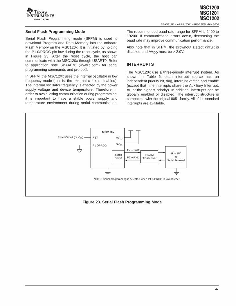
#$#$#$$
SBAS317E − APRIL 2004 − REVISED MAY 2006
www.ti.com
37
Serial Flash Programming Mode
Serial Flash Programming mode (SFPM) is used todownload Program and Data Memory into the onboardFlash Memory on the MSC120x. It is initiated by holdingthe P1.0/PROG pin low during the reset cycle, as shownin Figure 23. After the reset cycle, the host cancommunicate with the MSC120x through USART0. Referto application note SBAA076 (www.ti.com) for serialprogramming commands and protocol.
In SFPM, the MSC120x uses the internal oscillator in lowfrequency mode (that is, the external clock is disabled).The internal oscillator frequency is affected by the powersupply voltage and device temperature. Therefore, inorder to avoid losing communication during programming,it is important to have a stable power supply andtemperature environment during serial communication.
The recommended baud rate range for SFPM is 2400 to19200. If communication errors occur, decreasing thebaud rate may improve communication performance.
Also note that in SFPM, the Brownout Detect circuit isdisabled and AVDD must be > 2.0V.
INTERRUPTS
The MSC120x use a three-priority interrupt system. Asshown in Table 6, each interrupt source has anindependent priority bit, flag, interrupt vector, and enable(except that nine interrupts share the Auxiliary Interrupt,AI, at the highest priority). In addition, interrupts can beglobally enabled or disabled. The interrupt structure iscompatible with the original 8051 family. All of the standardinterrupts are available.
MSC120x
P1.0/PROG
P3.0 RXD
P3.1 TXD
SerialPort 0
RST
DVDD
Reset Circuit (or VDD)
RS232Transceiver
Host PCor
Serial Terminal
AVDD
NOTE: Serial programming is selected when P1.0/PROG is low at reset.
Figure 23. Serial Flash Programming Mode
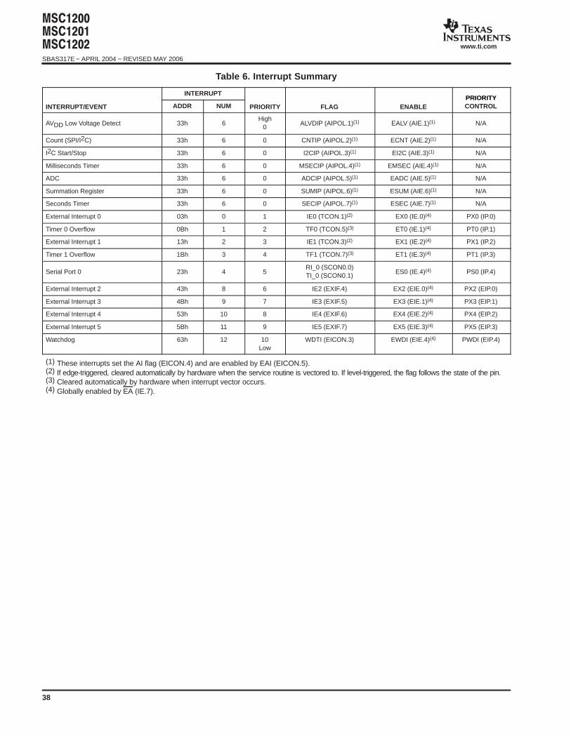
#$#$#$$SBAS317E − APRIL 2004 − REVISED MAY 2006
www.ti.com
38
Table 6. Interrupt Summary
INTERRUPTPRIORITY
INTERRUPT/EVENT ADDR NUM PRIORITY FLAG ENABLEPRIORITYCONTROL
AVDD Low Voltage Detect 33h 6High
0ALVDIP (AIPOL.1)(1) EALV (AIE.1)(1) N/A
Count (SPI/I2C) 33h 6 0 CNTIP (AIPOL.2)(1) ECNT (AIE.2)(1) N/A
I2C Start/Stop 33h 6 0 I2CIP (AIPOL.3)(1) EI2C (AIE.3)(1) N/A
Milliseconds Timer 33h 6 0 MSECIP (AIPOL.4)(1) EMSEC (AIE.4)(1) N/A
ADC 33h 6 0 ADCIP (AIPOL.5)(1) EADC (AIE.5)(1) N/A
Summation Register 33h 6 0 SUMIP (AIPOL.6)(1) ESUM (AIE.6)(1) N/A
Seconds Timer 33h 6 0 SECIP (AIPOL.7)(1) ESEC (AIE.7)(1) N/A
External Interrupt 0 03h 0 1 IE0 (TCON.1)(2) EX0 (IE.0)(4) PX0 (IP.0)
Timer 0 Overflow 0Bh 1 2 TF0 (TCON.5)(3) ET0 (IE.1)(4) PT0 (IP.1)
External Interrupt 1 13h 2 3 IE1 (TCON.3)(2) EX1 (IE.2)(4) PX1 (IP.2)
Timer 1 Overflow 1Bh 3 4 TF1 (TCON.7)(3) ET1 (IE.3)(4) PT1 (IP.3)
Serial Port 0 23h 4 5RI_0 (SCON0.0)TI_0 (SCON0.1)
ES0 (IE.4)(4) PS0 (IP.4)
External Interrupt 2 43h 8 6 IE2 (EXIF.4) EX2 (EIE.0)(4) PX2 (EIP.0)
External Interrupt 3 4Bh 9 7 IE3 (EXIF.5) EX3 (EIE.1)(4) PX3 (EIP.1)
External Interrupt 4 53h 10 8 IE4 (EXIF.6) EX4 (EIE.2)(4) PX4 (EIP.2)
External Interrupt 5 5Bh 11 9 IE5 (EXIF.7) EX5 (EIE.3)(4) PX5 (EIP.3)
Watchdog 63h 12 10Low
WDTI (EICON.3) EWDI (EIE.4)(4) PWDI (EIP.4)
(1) These interrupts set the AI flag (EICON.4) and are enabled by EAI (EICON.5).(2) If edge-triggered, cleared automatically by hardware when the service routine is vectored to. If level-triggered, the flag follows the state of the pin.(3) Cleared automatically by hardware when interrupt vector occurs.(4) Globally enabled by EA (IE.7).
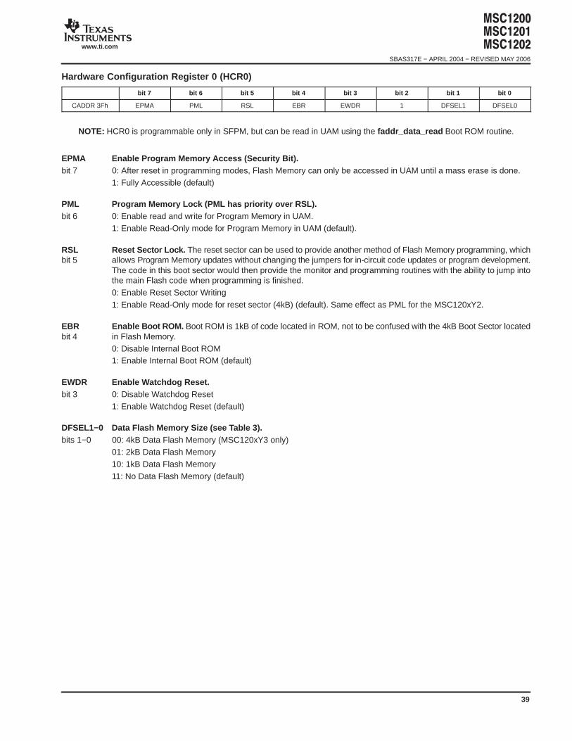
#$#$#$$
SBAS317E − APRIL 2004 − REVISED MAY 2006
www.ti.com
39
Hardware Configuration Register 0 (HCR0)
bit 7 bit 6 bit 5 bit 4 bit 3 bit 2 bit 1 bit 0
CADDR 3Fh EPMA PML RSL EBR EWDR 1 DFSEL1 DFSEL0
NOTE: HCR0 is programmable only in SFPM, but can be read in UAM using the faddr_data_read Boot ROM routine.
EPMA Enable Program Memory Access (Security Bit).bit 7 0: After reset in programming modes, Flash Memory can only be accessed in UAM until a mass erase is done.
1: Fully Accessible (default)
PML Program Memory Lock (PML has priority over RSL).bit 6 0: Enable read and write for Program Memory in UAM.
1: Enable Read-Only mode for Program Memory in UAM (default).
RSL Reset Sector Lock. The reset sector can be used to provide another method of Flash Memory programming, whichbit 5 allows Program Memory updates without changing the jumpers for in-circuit code updates or program development.
The code in this boot sector would then provide the monitor and programming routines with the ability to jump intothe main Flash code when programming is finished.0: Enable Reset Sector Writing1: Enable Read-Only mode for reset sector (4kB) (default). Same effect as PML for the MSC120xY2.
EBR Enable Boot ROM. Boot ROM is 1kB of code located in ROM, not to be confused with the 4kB Boot Sector locatedbit 4 in Flash Memory.
0: Disable Internal Boot ROM1: Enable Internal Boot ROM (default)
EWDR Enable Watchdog Reset.bit 3 0: Disable Watchdog Reset
1: Enable Watchdog Reset (default)
DFSEL1−0 Data Flash Memory Size (see Table 3).bits 1−0 00: 4kB Data Flash Memory (MSC120xY3 only)
01: 2kB Data Flash Memory10: 1kB Data Flash Memory11: No Data Flash Memory (default)
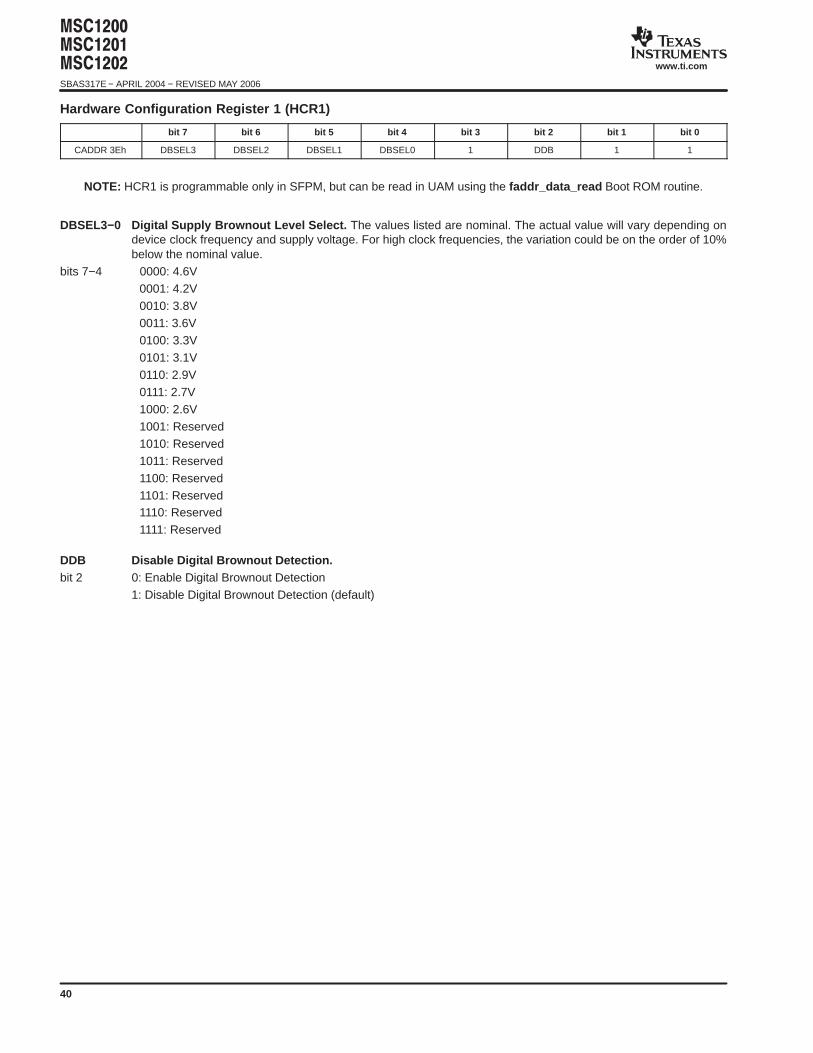
#$#$#$$SBAS317E − APRIL 2004 − REVISED MAY 2006
www.ti.com
40
Hardware Configuration Register 1 (HCR1)
bit 7 bit 6 bit 5 bit 4 bit 3 bit 2 bit 1 bit 0
CADDR 3Eh DBSEL3 DBSEL2 DBSEL1 DBSEL0 1 DDB 1 1
NOTE: HCR1 is programmable only in SFPM, but can be read in UAM using the faddr_data_read Boot ROM routine.
DBSEL3−0 Digital Supply Brownout Level Select. The values listed are nominal. The actual value will vary depending ondevice clock frequency and supply voltage. For high clock frequencies, the variation could be on the order of 10%below the nominal value.
bits 7−4 0000: 4.6V0001: 4.2V0010: 3.8V0011: 3.6V0100: 3.3V0101: 3.1V0110: 2.9V0111: 2.7V1000: 2.6V1001: Reserved1010: Reserved1011: Reserved1100: Reserved1101: Reserved1110: Reserved1111: Reserved
DDB Disable Digital Brownout Detection.bit 2 0: Enable Digital Brownout Detection
1: Disable Digital Brownout Detection (default)
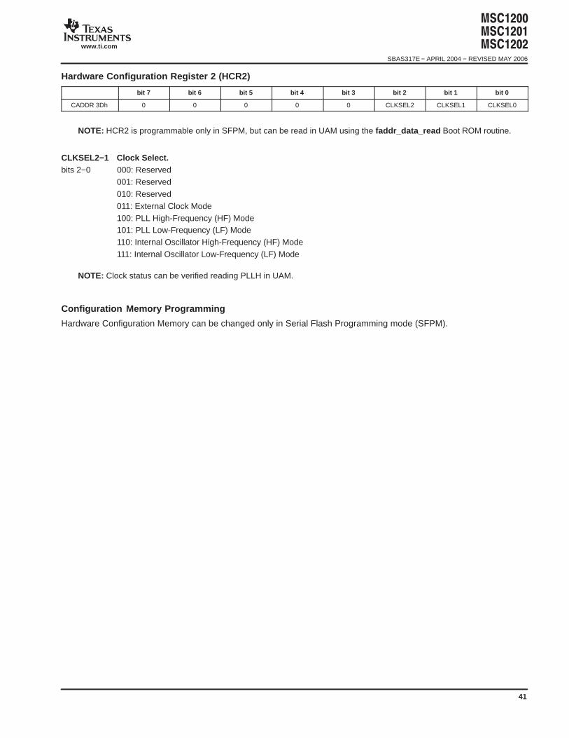
#$#$#$$
SBAS317E − APRIL 2004 − REVISED MAY 2006
www.ti.com
41
Hardware Configuration Register 2 (HCR2)
bit 7 bit 6 bit 5 bit 4 bit 3 bit 2 bit 1 bit 0
CADDR 3Dh 0 0 0 0 0 CLKSEL2 CLKSEL1 CLKSEL0
NOTE: HCR2 is programmable only in SFPM, but can be read in UAM using the faddr_data_read Boot ROM routine.
CLKSEL2−1 Clock Select.bits 2−0 000: Reserved
001: Reserved010: Reserved011: External Clock Mode100: PLL High-Frequency (HF) Mode101: PLL Low-Frequency (LF) Mode110: Internal Oscillator High-Frequency (HF) Mode111: Internal Oscillator Low-Frequency (LF) Mode
NOTE: Clock status can be verified reading PLLH in UAM.
Configuration Memory Programming
Hardware Configuration Memory can be changed only in Serial Flash Programming mode (SFPM).
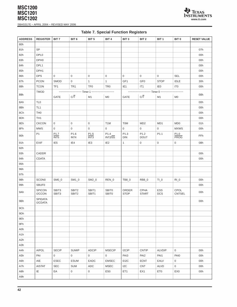
#$#$#$$SBAS317E − APRIL 2004 − REVISED MAY 2006
www.ti.com
42
Table 7. Special Function Registers
ADDRESS REGISTER BIT 7 BIT 6 BIT 5 BIT 4 BIT 3 BIT 2 BIT 1 BIT 0 RESET VALUE
80h
81h SP 07h
82h DPL0 00h
83h DPH0 00h
84h DPL1 00h
85h DPH1 00h
86h DPS 0 0 0 0 0 0 0 SEL 00h
87h PCON SMOD 0 1 1 GF1 GF0 STOP IDLE 30h
88h TCON TF1 TR1 TF0 TR0 IE1 IT1 IE0 IT0 00h
89hTMOD −−−−−−−−−−−−−−− Timer 1 −−−−−−−−−−−−−−− −−−−−−−−−−−−−−− Timer 0 −−−−−−−−−−−−−−−
00h89hTMOD
GATE C/T M1 M0 GATE C/T M1 M000h
8Ah TL0 00h
8Bh TL1 00h
8Ch TH0 00h
8Dh TH1 00h
8Eh CKCON 0 0 0 T1M T0M MD2 MD1 MD0 01h
8Fh MWS 0 0 0 0 0 0 0 MXWS 00h
90hP1 P1.7
INT5P1.6INT4
P1.5INT3
P1.4INT2/SS
P1.3DIN
P1.2DOUT
P1.1 P1.0PROG
FFh
91h EXIF IE5 IE4 IE3 IE2 1 0 0 0 08h
92h
93h CADDR 00h
94h CDATA 00h
95h
96h
97h
98h SCON0 SM0_0 SM1_0 SM2_0 REN_0 TB8_0 RB8_0 TI_0 RI_0 00h
99h SBUF0 00h
9AhSPICONI2CCON
SBIT3SBIT3
SBIT2SBIT2
SBIT1SBIT1
SBIT0SBIT0
ORDERSTOP
CPHASTART
ESSDCS
CPOLCNTSEL
00h
9BhSPIDATAI2CDATA
00h
9Ch
9Dh
9Eh
9Fh
A0h
A1h
A2h
A3h
A4h AIPOL SECIP SUMIP ADCIP MSECIP I2CIP CNTIP ALVDIP 0 00h
A5h PAI 0 0 0 0 PAI3 PAI2 PAI1 PAI0 00h
A6h AIE ESEC ESUM EADC EMSEC EI2C ECNT EALV 0 00h
A7h AISTAT SEC SUM ADC MSEC I2C CNT ALVD 0 00h
A8h IE EA 0 0 ES0 ET1 EX1 ET0 EX0 00h
A9h
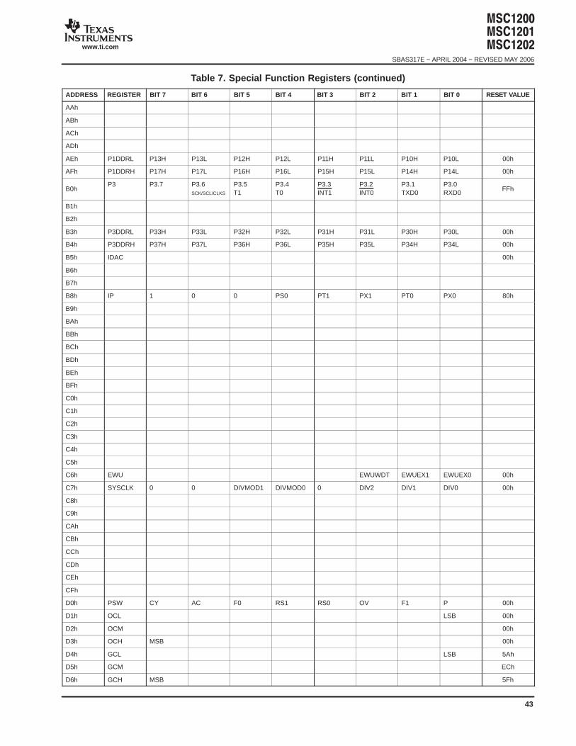
#$#$#$$
SBAS317E − APRIL 2004 − REVISED MAY 2006
www.ti.com
43
Table 7. Special Function Registers (continued)
ADDRESS RESET VALUEBIT 0BIT 1BIT 2BIT 3BIT 4BIT 5BIT 6BIT 7REGISTER
AAh
ABh
ACh
ADh
AEh P1DDRL P13H P13L P12H P12L P11H P11L P10H P10L 00h
AFh P1DDRH P17H P17L P16H P16L P15H P15L P14H P14L 00h
B0hP3 P3.7 P3.6
SCK/SCL/CLKS
P3.5T1
P3.4T0
P3.3INT1
P3.2INT0
P3.1TXD0
P3.0RXD0
FFh
B1h
B2h
B3h P3DDRL P33H P33L P32H P32L P31H P31L P30H P30L 00h
B4h P3DDRH P37H P37L P36H P36L P35H P35L P34H P34L 00h
B5h IDAC 00h
B6h
B7h
B8h IP 1 0 0 PS0 PT1 PX1 PT0 PX0 80h
B9h
BAh
BBh
BCh
BDh
BEh
BFh
C0h
C1h
C2h
C3h
C4h
C5h
C6h EWU EWUWDT EWUEX1 EWUEX0 00h
C7h SYSCLK 0 0 DIVMOD1 DIVMOD0 0 DIV2 DIV1 DIV0 00h
C8h
C9h
CAh
CBh
CCh
CDh
CEh
CFh
D0h PSW CY AC F0 RS1 RS0 OV F1 P 00h
D1h OCL LSB 00h
D2h OCM 00h
D3h OCH MSB 00h
D4h GCL LSB 5Ah
D5h GCM ECh
D6h GCH MSB 5Fh
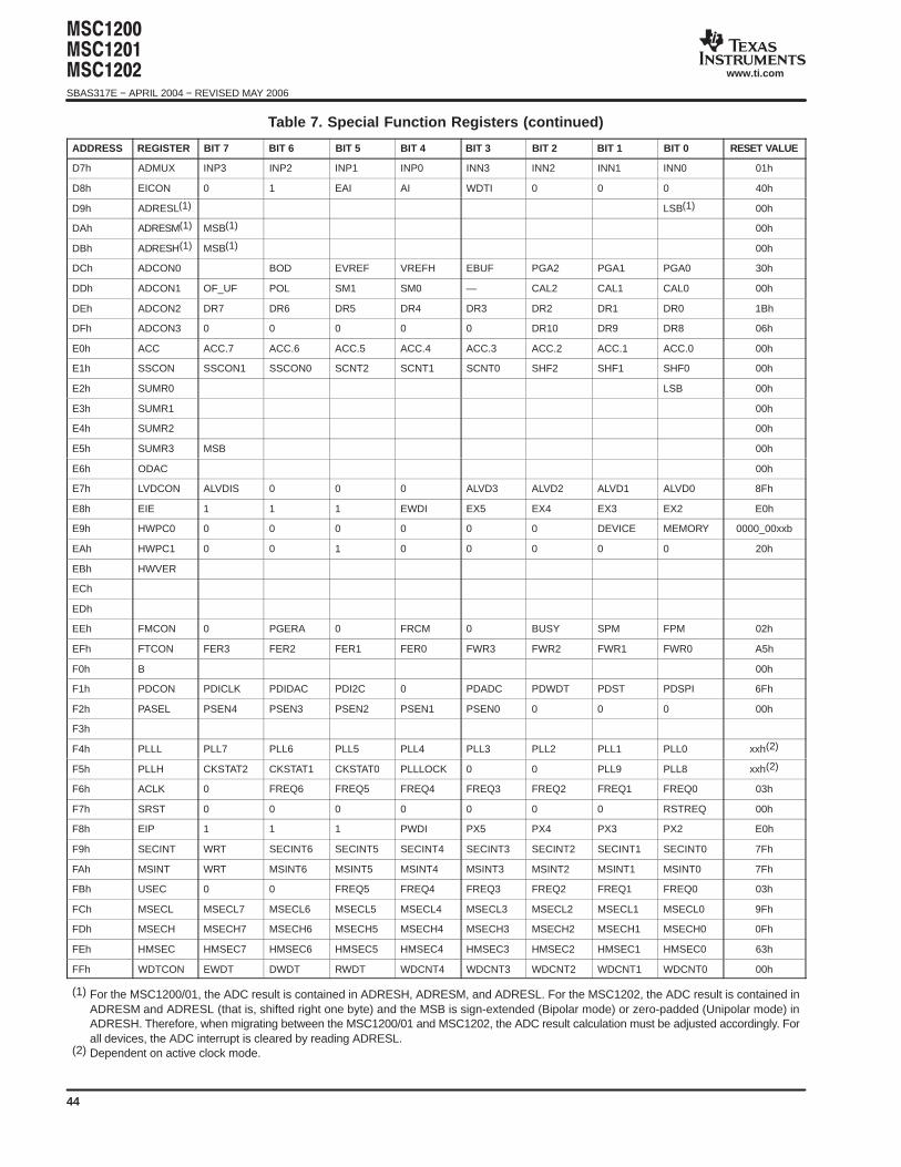
#$#$#$$SBAS317E − APRIL 2004 − REVISED MAY 2006
www.ti.com
44
Table 7. Special Function Registers (continued)
ADDRESS RESET VALUEBIT 0BIT 1BIT 2BIT 3BIT 4BIT 5BIT 6BIT 7REGISTER
D7h ADMUX INP3 INP2 INP1 INP0 INN3 INN2 INN1 INN0 01h
D8h EICON 0 1 EAI AI WDTI 0 0 0 40h
D9h ADRESL(1) LSB(1) 00h
DAh ADRESM(1) MSB(1) 00h
DBh ADRESH(1) MSB(1) 00h
DCh ADCON0 BOD EVREF VREFH EBUF PGA2 PGA1 PGA0 30h
DDh ADCON1 OF_UF POL SM1 SM0 — CAL2 CAL1 CAL0 00h
DEh ADCON2 DR7 DR6 DR5 DR4 DR3 DR2 DR1 DR0 1Bh
DFh ADCON3 0 0 0 0 0 DR10 DR9 DR8 06h
E0h ACC ACC.7 ACC.6 ACC.5 ACC.4 ACC.3 ACC.2 ACC.1 ACC.0 00h
E1h SSCON SSCON1 SSCON0 SCNT2 SCNT1 SCNT0 SHF2 SHF1 SHF0 00h
E2h SUMR0 LSB 00h
E3h SUMR1 00h
E4h SUMR2 00h
E5h SUMR3 MSB 00h
E6h ODAC 00h
E7h LVDCON ALVDIS 0 0 0 ALVD3 ALVD2 ALVD1 ALVD0 8Fh
E8h EIE 1 1 1 EWDI EX5 EX4 EX3 EX2 E0h
E9h HWPC0 0 0 0 0 0 0 DEVICE MEMORY 0000_00xxb
EAh HWPC1 0 0 1 0 0 0 0 0 20h
EBh HWVER
ECh
EDh
EEh FMCON 0 PGERA 0 FRCM 0 BUSY SPM FPM 02h
EFh FTCON FER3 FER2 FER1 FER0 FWR3 FWR2 FWR1 FWR0 A5h
F0h B 00h
F1h PDCON PDICLK PDIDAC PDI2C 0 PDADC PDWDT PDST PDSPI 6Fh
F2h PASEL PSEN4 PSEN3 PSEN2 PSEN1 PSEN0 0 0 0 00h
F3h
F4h PLLL PLL7 PLL6 PLL5 PLL4 PLL3 PLL2 PLL1 PLL0 xxh(2)
F5h PLLH CKSTAT2 CKSTAT1 CKSTAT0 PLLLOCK 0 0 PLL9 PLL8 xxh(2)
F6h ACLK 0 FREQ6 FREQ5 FREQ4 FREQ3 FREQ2 FREQ1 FREQ0 03h
F7h SRST 0 0 0 0 0 0 0 RSTREQ 00h
F8h EIP 1 1 1 PWDI PX5 PX4 PX3 PX2 E0h
F9h SECINT WRT SECINT6 SECINT5 SECINT4 SECINT3 SECINT2 SECINT1 SECINT0 7Fh
FAh MSINT WRT MSINT6 MSINT5 MSINT4 MSINT3 MSINT2 MSINT1 MSINT0 7Fh
FBh USEC 0 0 FREQ5 FREQ4 FREQ3 FREQ2 FREQ1 FREQ0 03h
FCh MSECL MSECL7 MSECL6 MSECL5 MSECL4 MSECL3 MSECL2 MSECL1 MSECL0 9Fh
FDh MSECH MSECH7 MSECH6 MSECH5 MSECH4 MSECH3 MSECH2 MSECH1 MSECH0 0Fh
FEh HMSEC HMSEC7 HMSEC6 HMSEC5 HMSEC4 HMSEC3 HMSEC2 HMSEC1 HMSEC0 63h
FFh WDTCON EWDT DWDT RWDT WDCNT4 WDCNT3 WDCNT2 WDCNT1 WDCNT0 00h
(1) For the MSC1200/01, the ADC result is contained in ADRESH, ADRESM, and ADRESL. For the MSC1202, the ADC result is contained inADRESM and ADRESL (that is, shifted right one byte) and the MSB is sign-extended (Bipolar mode) or zero-padded (Unipolar mode) inADRESH. Therefore, when migrating between the MSC1200/01 and MSC1202, the ADC result calculation must be adjusted accordingly. Forall devices, the ADC interrupt is cleared by reading ADRESL.
(2) Dependent on active clock mode.
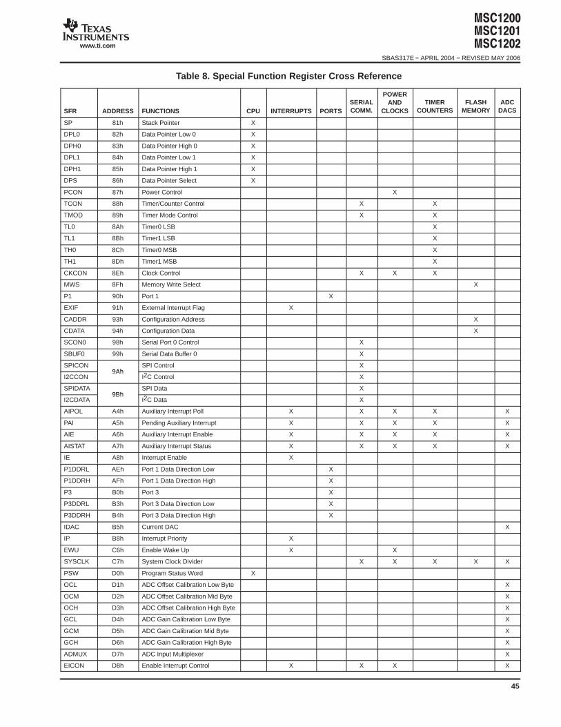
#$#$#$$
SBAS317E − APRIL 2004 − REVISED MAY 2006
www.ti.com
45
Table 8. Special Function Register Cross Reference
SFR ADDRESS FUNCTIONS CPU INTERRUPTS PORTSSERIALCOMM.
POWERAND
CLOCKSTIMER
COUNTERSFLASH
MEMORYADC
DACS
SP 81h Stack Pointer X
DPL0 82h Data Pointer Low 0 X
DPH0 83h Data Pointer High 0 X
DPL1 84h Data Pointer Low 1 X
DPH1 85h Data Pointer High 1 X
DPS 86h Data Pointer Select X
PCON 87h Power Control X
TCON 88h Timer/Counter Control X X
TMOD 89h Timer Mode Control X X
TL0 8Ah Timer0 LSB X
TL1 8Bh Timer1 LSB X
TH0 8Ch Timer0 MSB X
TH1 8Dh Timer1 MSB X
CKCON 8Eh Clock Control X X X
MWS 8Fh Memory Write Select X
P1 90h Port 1 X
EXIF 91h External Interrupt Flag X
CADDR 93h Configuration Address X
CDATA 94h Configuration Data X
SCON0 98h Serial Port 0 Control X
SBUF0 99h Serial Data Buffer 0 X
SPICON9Ah
SPI Control X
I2CCON9Ah
I2C Control X
SPIDATA9Bh
SPI Data X
I2CDATA9Bh
I2C Data X
AIPOL A4h Auxiliary Interrupt Poll X X X X X
PAI A5h Pending Auxiliary Interrupt X X X X X
AIE A6h Auxiliary Interrupt Enable X X X X X
AISTAT A7h Auxiliary Interrupt Status X X X X X
IE A8h Interrupt Enable X
P1DDRL AEh Port 1 Data Direction Low X
P1DDRH AFh Port 1 Data Direction High X
P3 B0h Port 3 X
P3DDRL B3h Port 3 Data Direction Low X
P3DDRH B4h Port 3 Data Direction High X
IDAC B5h Current DAC X
IP B8h Interrupt Priority X
EWU C6h Enable Wake Up X X
SYSCLK C7h System Clock Divider X X X X X
PSW D0h Program Status Word X
OCL D1h ADC Offset Calibration Low Byte X
OCM D2h ADC Offset Calibration Mid Byte X
OCH D3h ADC Offset Calibration High Byte X
GCL D4h ADC Gain Calibration Low Byte X
GCM D5h ADC Gain Calibration Mid Byte X
GCH D6h ADC Gain Calibration High Byte X
ADMUX D7h ADC Input Multiplexer X
EICON D8h Enable Interrupt Control X X X X
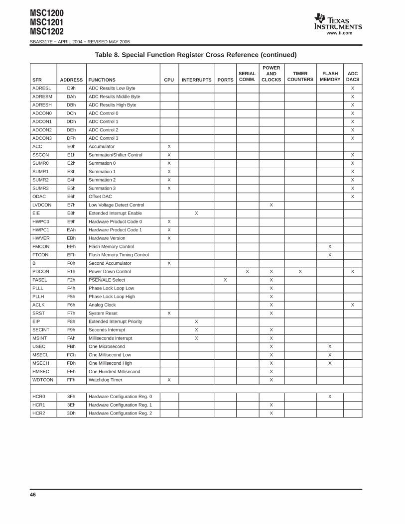
#$#$#$$SBAS317E − APRIL 2004 − REVISED MAY 2006
www.ti.com
46
Table 8. Special Function Register Cross Reference (continued)
SFRADC
DACSFLASH
MEMORYTIMER
COUNTERS
POWERAND
CLOCKSSERIALCOMM.PORTSINTERRUPTSCPUFUNCTIONSADDRESS
ADRESL D9h ADC Results Low Byte X
ADRESM DAh ADC Results Middle Byte X
ADRESH DBh ADC Results High Byte X
ADCON0 DCh ADC Control 0 X
ADCON1 DDh ADC Control 1 X
ADCON2 DEh ADC Control 2 X
ADCON3 DFh ADC Control 3 X
ACC E0h Accumulator X
SSCON E1h Summation/Shifter Control X X
SUMR0 E2h Summation 0 X X
SUMR1 E3h Summation 1 X X
SUMR2 E4h Summation 2 X X
SUMR3 E5h Summation 3 X X
ODAC E6h Offset DAC X
LVDCON E7h Low Voltage Detect Control X
EIE E8h Extended Interrupt Enable X
HWPC0 E9h Hardware Product Code 0 X
HWPC1 EAh Hardware Product Code 1 X
HWVER EBh Hardware Version X
FMCON EEh Flash Memory Control X
FTCON EFh Flash Memory Timing Control X
B F0h Second Accumulator X
PDCON F1h Power Down Control X X X X
PASEL F2h PSEN/ALE Select X X
PLLL F4h Phase Lock Loop Low X
PLLH F5h Phase Lock Loop High X
ACLK F6h Analog Clock X X
SRST F7h System Reset X X
EIP F8h Extended Interrupt Priority X
SECINT F9h Seconds Interrupt X X
MSINT FAh Milliseconds Interrupt X X
USEC FBh One Microsecond X X
MSECL FCh One Millisecond Low X X
MSECH FDh One Millisecond High X X
HMSEC FEh One Hundred Millisecond X
WDTCON FFh Watchdog Timer X X
HCR0 3Fh Hardware Configuration Reg. 0 X
HCR1 3Eh Hardware Configuration Reg. 1 X
HCR2 3Dh Hardware Configuration Reg. 2 X
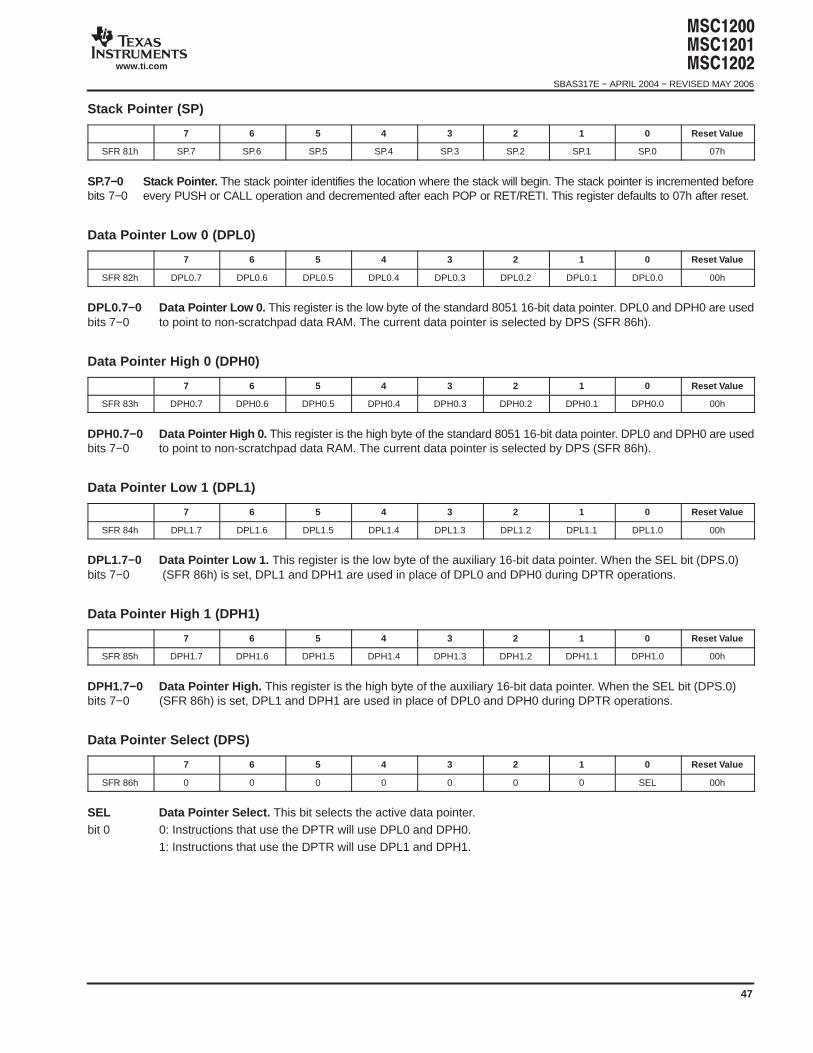
#$#$#$$
SBAS317E − APRIL 2004 − REVISED MAY 2006
www.ti.com
47
Stack Pointer (SP)
7 6 5 4 3 2 1 0 Reset Value
SFR 81h SP.7 SP.6 SP.5 SP.4 SP.3 SP.2 SP.1 SP.0 07h
SP.7−0 Stack Pointer. The stack pointer identifies the location where the stack will begin. The stack pointer is incremented beforebits 7−0 every PUSH or CALL operation and decremented after each POP or RET/RETI. This register defaults to 07h after reset.
Data Pointer Low 0 (DPL0)
7 6 5 4 3 2 1 0 Reset Value
SFR 82h DPL0.7 DPL0.6 DPL0.5 DPL0.4 DPL0.3 DPL0.2 DPL0.1 DPL0.0 00h
DPL0.7−0 Data Pointer Low 0. This register is the low byte of the standard 8051 16-bit data pointer. DPL0 and DPH0 are usedbits 7−0 to point to non-scratchpad data RAM. The current data pointer is selected by DPS (SFR 86h).
Data Pointer High 0 (DPH0)
7 6 5 4 3 2 1 0 Reset Value
SFR 83h DPH0.7 DPH0.6 DPH0.5 DPH0.4 DPH0.3 DPH0.2 DPH0.1 DPH0.0 00h
DPH0.7−0 Data Pointer High 0. This register is the high byte of the standard 8051 16-bit data pointer. DPL0 and DPH0 are usedbits 7−0 to point to non-scratchpad data RAM. The current data pointer is selected by DPS (SFR 86h).
Data Pointer Low 1 (DPL1)
7 6 5 4 3 2 1 0 Reset Value
SFR 84h DPL1.7 DPL1.6 DPL1.5 DPL1.4 DPL1.3 DPL1.2 DPL1.1 DPL1.0 00h
DPL1.7−0 Data Pointer Low 1. This register is the low byte of the auxiliary 16-bit data pointer. When the SEL bit (DPS.0)bits 7−0 (SFR 86h) is set, DPL1 and DPH1 are used in place of DPL0 and DPH0 during DPTR operations.
Data Pointer High 1 (DPH1)
7 6 5 4 3 2 1 0 Reset Value
SFR 85h DPH1.7 DPH1.6 DPH1.5 DPH1.4 DPH1.3 DPH1.2 DPH1.1 DPH1.0 00h
DPH1.7−0 Data Pointer High. This register is the high byte of the auxiliary 16-bit data pointer. When the SEL bit (DPS.0)bits 7−0 (SFR 86h) is set, DPL1 and DPH1 are used in place of DPL0 and DPH0 during DPTR operations.
Data Pointer Select (DPS)
7 6 5 4 3 2 1 0 Reset Value
SFR 86h 0 0 0 0 0 0 0 SEL 00h
SEL Data Pointer Select. This bit selects the active data pointer.bit 0 0: Instructions that use the DPTR will use DPL0 and DPH0.
1: Instructions that use the DPTR will use DPL1 and DPH1.
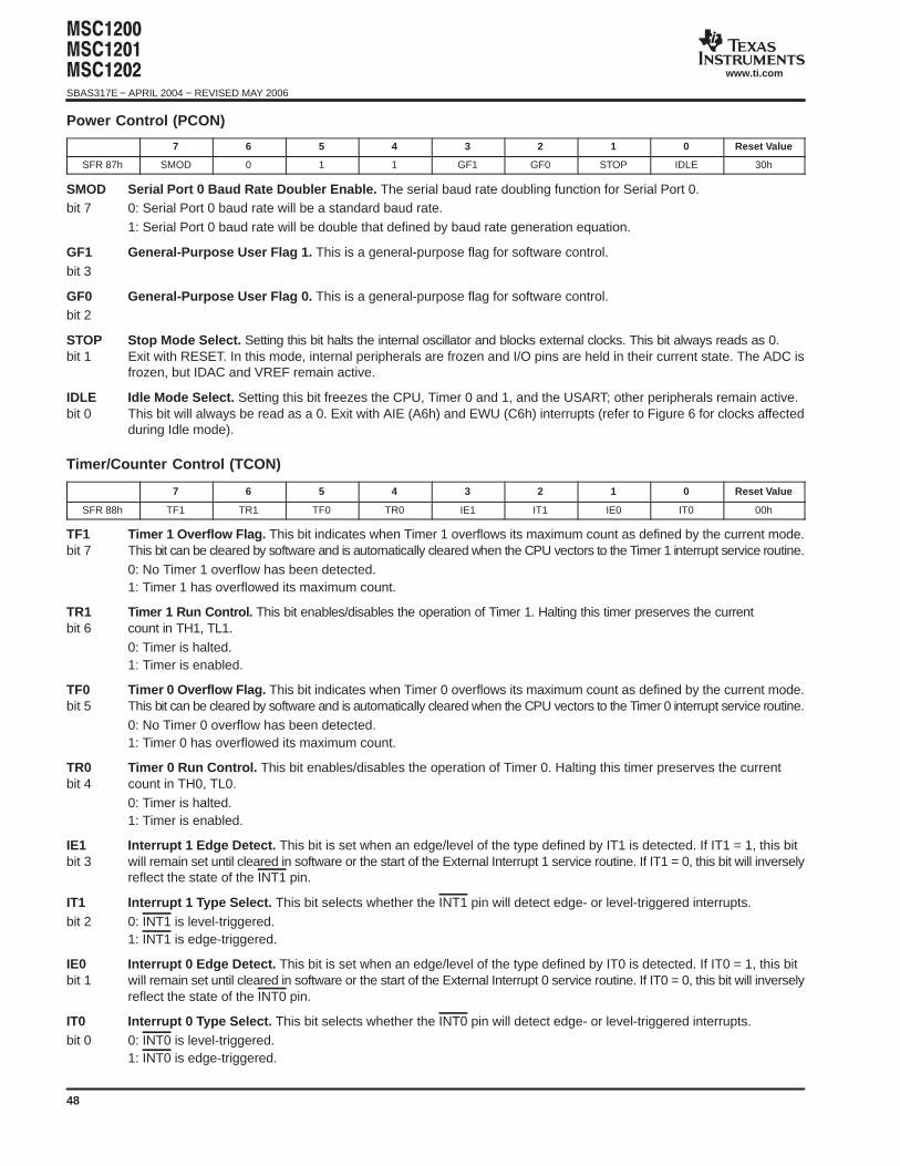
#$#$#$$SBAS317E − APRIL 2004 − REVISED MAY 2006
www.ti.com
48
Power Control (PCON)
7 6 5 4 3 2 1 0 Reset Value
SFR 87h SMOD 0 1 1 GF1 GF0 STOP IDLE 30h
SMOD Serial Port 0 Baud Rate Doubler Enable. The serial baud rate doubling function for Serial Port 0.bit 7 0: Serial Port 0 baud rate will be a standard baud rate.
1: Serial Port 0 baud rate will be double that defined by baud rate generation equation.
GF1 General-Purpose User Flag 1. This is a general-purpose flag for software control.bit 3
GF0 General-Purpose User Flag 0. This is a general-purpose flag for software control.bit 2
STOP Stop Mode Select. Setting this bit halts the internal oscillator and blocks external clocks. This bit always reads as 0.bit 1 Exit with RESET. In this mode, internal peripherals are frozen and I/O pins are held in their current state. The ADC is
frozen, but IDAC and VREF remain active.
IDLE Idle Mode Select. Setting this bit freezes the CPU, Timer 0 and 1, and the USART; other peripherals remain active.bit 0 This bit will always be read as a 0. Exit with AIE (A6h) and EWU (C6h) interrupts (refer to Figure 6 for clocks affected
during Idle mode).
Timer/Counter Control (TCON)
7 6 5 4 3 2 1 0 Reset Value
SFR 88h TF1 TR1 TF0 TR0 IE1 IT1 IE0 IT0 00h
TF1 Timer 1 Overflow Flag. This bit indicates when Timer 1 overflows its maximum count as defined by the current mode.bit 7 This bit can be cleared by software and is automatically cleared when the CPU vectors to the Timer 1 interrupt service routine.
0: No Timer 1 overflow has been detected.1: Timer 1 has overflowed its maximum count.
TR1 Timer 1 Run Control. This bit enables/disables the operation of Timer 1. Halting this timer preserves the currentbit 6 count in TH1, TL1.
0: Timer is halted.1: Timer is enabled.
TF0 Timer 0 Overflow Flag. This bit indicates when Timer 0 overflows its maximum count as defined by the current mode.bit 5 This bit can be cleared by software and is automatically cleared when the CPU vectors to the Timer 0 interrupt service routine.
0: No Timer 0 overflow has been detected.1: Timer 0 has overflowed its maximum count.
TR0 Timer 0 Run Control. This bit enables/disables the operation of Timer 0. Halting this timer preserves the currentbit 4 count in TH0, TL0.
0: Timer is halted.1: Timer is enabled.
IE1 Interrupt 1 Edge Detect. This bit is set when an edge/level of the type defined by IT1 is detected. If IT1 = 1, this bitbit 3 will remain set until cleared in software or the start of the External Interrupt 1 service routine. If IT1 = 0, this bit will inversely
reflect the state of the INT1 pin.
IT1 Interrupt 1 Type Select. This bit selects whether the INT1 pin will detect edge- or level-triggered interrupts.bit 2 0: INT1 is level-triggered.
1: INT1 is edge-triggered.
IE0 Interrupt 0 Edge Detect. This bit is set when an edge/level of the type defined by IT0 is detected. If IT0 = 1, this bitbit 1 will remain set until cleared in software or the start of the External Interrupt 0 service routine. If IT0 = 0, this bit will inversely
reflect the state of the INT0 pin.
IT0 Interrupt 0 Type Select. This bit selects whether the INT0 pin will detect edge- or level-triggered interrupts.bit 0 0: INT0 is level-triggered.
1: INT0 is edge-triggered.
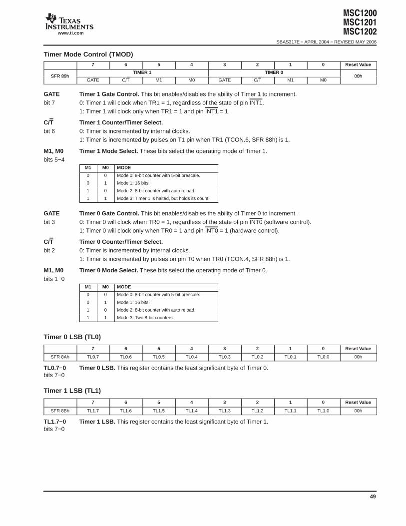
#$#$#$$
SBAS317E − APRIL 2004 − REVISED MAY 2006
www.ti.com
49
Timer Mode Control (TMOD)7 6 5 4 3 2 1 0 Reset Value
SFR 89hTIMER 1 TIMER 0
00hSFR 89hGATE C/T M1 M0 GATE C/T M1 M0
00h
GATE Timer 1 Gate Control. This bit enables/disables the ability of Timer 1 to increment.bit 7 0: Timer 1 will clock when TR1 = 1, regardless of the state of pin INT1.
1: Timer 1 will clock only when TR1 = 1 and pin INT1 = 1.
C/T Timer 1 Counter/Timer Select.bit 6 0: Timer is incremented by internal clocks.
1: Timer is incremented by pulses on T1 pin when TR1 (TCON.6, SFR 88h) is 1.
M1, M0 Timer 1 Mode Select. These bits select the operating mode of Timer 1.bits 5−4
M1 M0 MODE
0 0 Mode 0: 8-bit counter with 5-bit prescale.
0 1 Mode 1: 16 bits.
1 0 Mode 2: 8-bit counter with auto reload.
1 1 Mode 3: Timer 1 is halted, but holds its count.
GATE Timer 0 Gate Control. This bit enables/disables the ability of Timer 0 to increment.bit 3 0: Timer 0 will clock when TR0 = 1, regardless of the state of pin INT0 (software control).
1: Timer 0 will clock only when TR0 = 1 and pin INT0 = 1 (hardware control).
C/T Timer 0 Counter/Timer Select.bit 2 0: Timer is incremented by internal clocks.
1: Timer is incremented by pulses on pin T0 when TR0 (TCON.4, SFR 88h) is 1.
M1, M0 Timer 0 Mode Select. These bits select the operating mode of Timer 0.bits 1−0
M1 M0 MODE
0 0 Mode 0: 8-bit counter with 5-bit prescale.
0 1 Mode 1: 16 bits.
1 0 Mode 2: 8-bit counter with auto reload.
1 1 Mode 3: Two 8-bit counters.
Timer 0 LSB (TL0)
7 6 5 4 3 2 1 0 Reset Value
SFR 8Ah TL0.7 TL0.6 TL0.5 TL0.4 TL0.3 TL0.2 TL0.1 TL0.0 00h
TL0.7−0 Timer 0 LSB. This register contains the least significant byte of Timer 0.bits 7−0
Timer 1 LSB (TL1)
7 6 5 4 3 2 1 0 Reset Value
SFR 8Bh TL1.7 TL1.6 TL1.5 TL1.4 TL1.3 TL1.2 TL1.1 TL1.0 00h
TL1.7−0 Timer 1 LSB. This register contains the least significant byte of Timer 1.bits 7−0
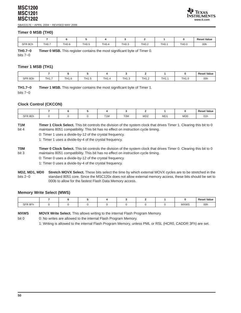
#$#$#$$SBAS317E − APRIL 2004 − REVISED MAY 2006
www.ti.com
50
Timer 0 MSB (TH0)
7 6 5 4 3 2 1 0 Reset Value
SFR 8Ch TH0.7 TH0.6 TH0.5 TH0.4 TH0.3 TH0.2 TH0.1 TH0.0 00h
TH0.7−0 Timer 0 MSB. This register contains the most significant byte of Timer 0.bits 7−0
Timer 1 MSB (TH1)
7 6 5 4 3 2 1 0 Reset Value
SFR 8Dh TH1.7 TH1.6 TH1.5 TH1.4 TH1.3 TH1.2 TH1.1 TH1.0 00h
TH1.7−0 Timer 1 MSB. This register contains the most significant byte of Timer 1.bits 7−0
Clock Control (CKCON)
7 6 5 4 3 2 1 0 Reset Value
SFR 8Eh 0 0 0 T1M T0M MD2 MD1 MD0 01h
T1M Timer 1 Clock Select. This bit controls the division of the system clock that drives Timer 1. Clearing this bit to 0bit 4 maintains 8051 compatibility. This bit has no effect on instruction cycle timing.
0: Timer 1 uses a divide-by-12 of the crystal frequency.1: Timer 1 uses a divide-by-4 of the crystal frequency.
T0M Timer 0 Clock Select. This bit controls the division of the system clock that drives Timer 0. Clearing this bit to 0bit 3 maintains 8051 compatibility. This bit has no effect on instruction cycle timing.
0: Timer 0 uses a divide-by-12 of the crystal frequency.1: Timer 0 uses a divide-by-4 of the crystal frequency.
MD2, MD1, MD0 Stretch MOVX Select. These bits select the time by which external MOVX cycles are to be stretched in thebits 2−0 standard 8051 core. Since the MSC120x does not allow external memory access, these bits should be set to
000b to allow for the fastest Flash Data Memory access.
Memory Write Select (MWS)
7 6 5 4 3 2 1 0 Reset Value
SFR 8Fh 0 0 0 0 0 0 0 MXWS 00h
MXWS MOVX Write Select. This allows writing to the internal Flash Program Memory.bit 0 0: No writes are allowed to the internal Flash Program Memory.
1: Writing is allowed to the internal Flash Program Memory, unless PML or RSL (HCR0, CADDR 3Fh) are set.
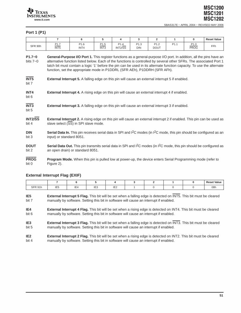
#$#$#$$
SBAS317E − APRIL 2004 − REVISED MAY 2006
www.ti.com
51
Port 1 (P1)
7 6 5 4 3 2 1 0 Reset Value
SFR 90hP1.7INT5
P1.6INT4
P1.5INT3
P1.4INT2/SS
P1.3DIN
P1.2DOUT
P1.1 P1.0PROG
FFh
P1.7−0 General-Purpose I/O Port 1. This register functions as a general-purpose I/O port. In addition, all the pins have anbits 7−0 alternative function listed below. Each of the functions is controlled by several other SFRs. The associated Port 1
latch bit must contain a logic ‘1’ before the pin can be used in its alternate function capacity. To use the alternatefunction, set the appropriate mode in P1DDRL (SFR AEh), P1DDRH (SFR AFh).
INT5 External Interrupt 5. A falling edge on this pin will cause an external interrupt 5 if enabled.bit 7
INT4 External Interrupt 4. A rising edge on this pin will cause an external interrupt 4 if enabled.bit 6
INT3 External Interrupt 3. A falling edge on this pin will cause an external interrupt 3 if enabled.bit 5
INT2/SS External Interrupt 2. A rising edge on this pin will cause an external interrupt 2 if enabled. This pin can be used asbit 4 slave select (SS) in SPI slave mode.
DIN Serial Data In. This pin receives serial data in SPI and I2C modes (in I2C mode, this pin should be configured as anbit 3 input) or standard 8051.
DOUT Serial Data Out. This pin transmits serial data in SPI and I2C modes (in I2C mode, this pin should be configured asbit 2 an open drain) or standard 8051.
PROG Program Mode. When this pin is pulled low at power-up, the device enters Serial Programming mode (refer tobit 0 Figure 2).
External Interrupt Flag (EXIF)
7 6 5 4 3 2 1 0 Reset Value
SFR 91h IE5 IE4 IE3 IE2 1 0 0 0 08h
IE5 External Interrupt 5 Flag. This bit will be set when a falling edge is detected on INT5. This bit must be clearedbit 7 manually by software. Setting this bit in software will cause an interrupt if enabled.
IE4 External Interrupt 4 Flag. This bit will be set when a rising edge is detected on INT4. This bit must be clearedbit 6 manually by software. Setting this bit in software will cause an interrupt if enabled.
IE3 External Interrupt 3 Flag. This bit will be set when a falling edge is detected on INT3. This bit must be clearedbit 5 manually by software. Setting this bit in software will cause an interrupt if enabled.
IE2 External Interrupt 2 Flag. This bit will be set when a rising edge is detected on INT2. This bit must be clearedbit 4 manually by software. Setting this bit in software will cause an interrupt if enabled.
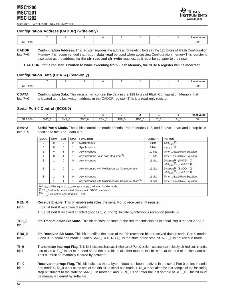
#$#$#$$SBAS317E − APRIL 2004 − REVISED MAY 2006
www.ti.com
52
Configuration Address (CADDR) (write-only)
7 6 5 4 3 2 1 0 Reset Value
SFR 93h 00h
CADDR Configuration Address. This register supplies the address for reading bytes in the 128 bytes of Flash Configurationbits 7−0 Memory. It is recommended that faddr_data_read be used when accessing Configuration memory.This register is
also used as the address for the sfr_read and sfr_write routines, so it must be set prior to their use.
CAUTION: If this register is written to while executing from Flash Memory, the CDATA register will be incorrect.
Configuration Data (CDATA) (read-only)
7 6 5 4 3 2 1 0 Reset Value
SFR 94h 00h
CDATA Configuration Data. This register will contain the data in the 128 bytes of Flash Configuration Memory thatbits 7−0 is located at the last written address in the CADDR register. This is a read-only register.
Serial Port 0 Control (SCON0)
7 6 5 4 3 2 1 0 Reset Value
SFR 98h SM0_0 SM1_0 SM2_0 REN_0 TB8_0 RB8_0 TI_0 RI_0 00h
SM0−2 Serial Port 0 Mode. These bits control the mode of serial Port 0. Modes 1, 2, and 3 have 1 start and 1 stop bit inbits 7−5 addition to the 8 or 9 data bits.
MODE SM0 SM1 SM2 FUNCTION LENGTH PERIOD
0 0 0 0 Synchronous 8 bits 12 pCLK(1)
0 0 0 1 Synchronous 8 bits 4 pCLK(1)
1 0 1 0 Asynchronous 10 bits Timer 1 Baud Rate Equation
1 0 1 1 Asynchronous−Valid Stop Required(2) 10 bits Timer 1 Baud Rate Equation
2 1 0 0 Asynchronous 11 bits 64 pCLK(1) (SMOD = 0)32 pCLK(1) (SMOD = 1)
2 1 0 1 Asynchronous with Multiprocessor Communication 11 bits 64 pCLK(1) (SMOD = 0)32 pCLK(1) (SMOD = 1)
3 1 1 0 Asynchronous 11 bits Timer 1 Baud Rate Equation
3 1 1 1 Asynchronous with Multiprocessor Communication(3) 11 bits Timer 1 Baud Rate Equation
(1) pCLK will be equal to tCLK, except that pCLK will stop for Idle mode.(2) RI_0 will only be activated when a valid STOP is received.(3) RI_0 will not be activated if bit 9 = 0.
REN_0 Receive Enable. This bit enables/disables the serial Port 0 received shift register.bit 4 0: Serial Port 0 reception disabled.
1: Serial Port 0 received enabled (modes 1, 2, and 3). Initiate synchronous reception (mode 0).
TB8_0 9th Transmission Bit State. This bit defines the state of the 9th transmission bit in serial Port 0 modes 2 and 3.bit 3
RB8_0 9th Received Bit State. This bit identifies the state of the 9th reception bit of received data in serial Port 0 modesbit 2 2 and 3. In serial port mode 1, when SM2_0 = 0, RB8_0 is the state of the stop bit. RB8_0 is not used in mode 0.
TI_0 Transmitter Interrupt Flag. This bit indicates that data in the serial Port 0 buffer has been completely shifted out. In serialbit 1 port mode 0, TI_0 is set at the end of the 8th data bit. In all other modes, this bit is set at the end of the last data bit.
This bit must be manually cleared by software.
RI_0 Receiver Interrupt Flag. This bit indicates that a byte of data has been received in the serial Port 0 buffer. In serialbit 0 port mode 0, RI_0 is set at the end of the 8th bit. In serial port mode 1, RI_0 is set after the last sample of the incoming
stop bit subject to the state of SM2_0. In modes 2 and 3, RI_0 is set after the last sample of RB8_0. This bit mustbe manually cleared by software.
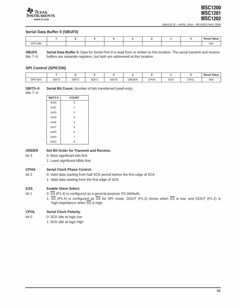
#$#$#$$
SBAS317E − APRIL 2004 − REVISED MAY 2006
www.ti.com
53
Serial Data Buffer 0 (SBUF0)
7 6 5 4 3 2 1 0 Reset Value
SFR 99h 00h
SBUF0 Serial Data Buffer 0. Data for Serial Port 0 is read from or written to this location. The serial transmit and receivebits 7−0 buffers are separate registers, but both are addressed at this location.
SPI Control (SPICON)
7 6 5 4 3 2 1 0 Reset Value
SFR 9Ah SBIT3 SBIT2 SBIT1 SBIT0 ORDER CPHA ESS CPOL 00h
SBIT3−0 Serial Bit Count. Number of bits transferred (read-only).bits 7−4
SBIT3:0 COUNT
0x00 0
0x01 1
0x03 2
0x02 3
0x06 4
0x07 5
0x05 6
0x04 7
0x0C 8
ORDER Set Bit Order for Transmit and Receive.bit 3 0: Most significant bits first
1: Least significant bBits first
CPHA Serial Clock Phase Control.bit 2 0: Valid data starting from half SCK period before the first edge of SCK
1: Valid data starting from the first edge of SCK
ESS Enable Slave Select.bit 1 0: SS (P1.4) is configured as a general-purpose I/O (default).
1: SS (P1.4) is configured as SS for SPI mode. DOUT (P1.2) drives when SS is low, and DOUT (P1.2) ishigh-impedance when SS is high.
CPOL Serial Clock Polarity.bit 0 0: SCK idle at logic low
1: SCK idle at logic high
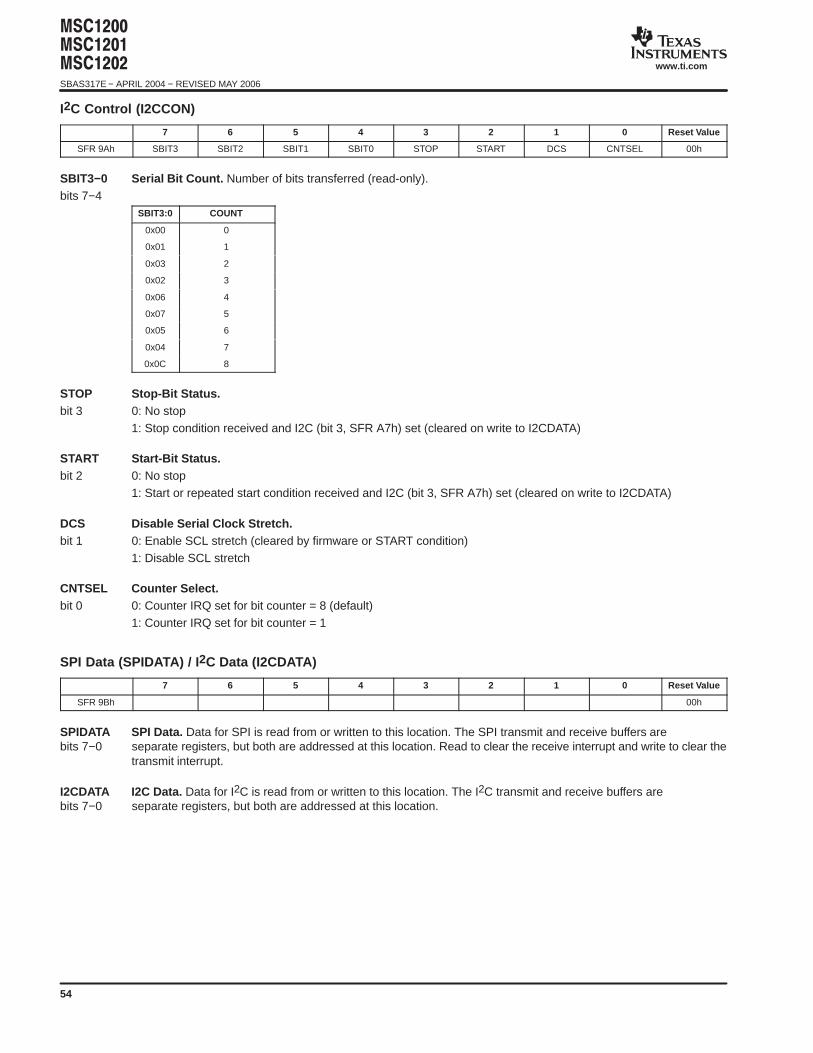
#$#$#$$SBAS317E − APRIL 2004 − REVISED MAY 2006
www.ti.com
54
I2C Control (I2CCON)
7 6 5 4 3 2 1 0 Reset Value
SFR 9Ah SBIT3 SBIT2 SBIT1 SBIT0 STOP START DCS CNTSEL 00h
SBIT3−0 Serial Bit Count. Number of bits transferred (read-only).bits 7−4
SBIT3:0 COUNT
0x00 0
0x01 1
0x03 2
0x02 3
0x06 4
0x07 5
0x05 6
0x04 7
0x0C 8
STOP Stop-Bit Status.bit 3 0: No stop
1: Stop condition received and I2C (bit 3, SFR A7h) set (cleared on write to I2CDATA)
START Start-Bit Status.bit 2 0: No stop
1: Start or repeated start condition received and I2C (bit 3, SFR A7h) set (cleared on write to I2CDATA)
DCS Disable Serial Clock Stretch.bit 1 0: Enable SCL stretch (cleared by firmware or START condition)
1: Disable SCL stretch
CNTSEL Counter Select.bit 0 0: Counter IRQ set for bit counter = 8 (default)
1: Counter IRQ set for bit counter = 1
SPI Data (SPIDATA) / I 2C Data (I2CDATA)
7 6 5 4 3 2 1 0 Reset Value
SFR 9Bh 00h
SPIDATA SPI Data. Data for SPI is read from or written to this location. The SPI transmit and receive buffers arebits 7−0 separate registers, but both are addressed at this location. Read to clear the receive interrupt and write to clear the
transmit interrupt.
I2CDATA I2C Data. Data for I2C is read from or written to this location. The I2C transmit and receive buffers arebits 7−0 separate registers, but both are addressed at this location.
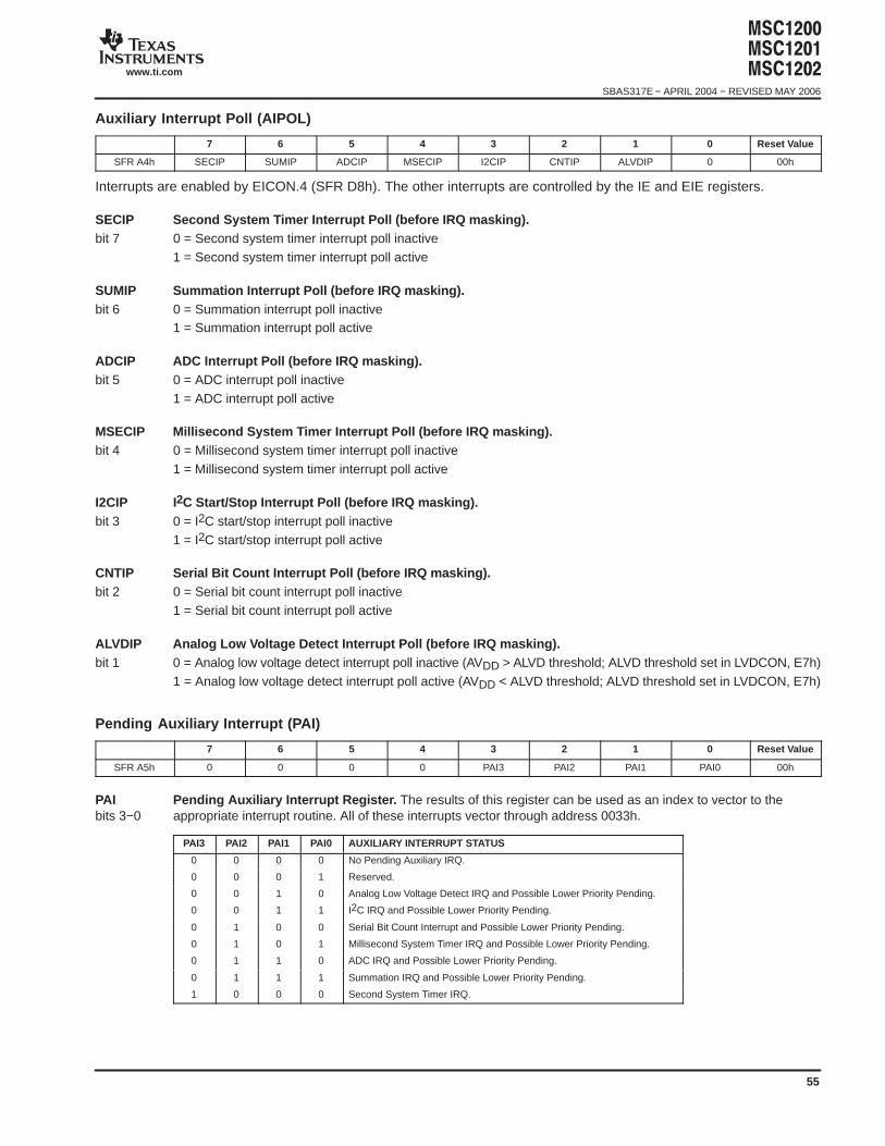
#$#$#$$
SBAS317E − APRIL 2004 − REVISED MAY 2006
www.ti.com
55
Auxiliary Interrupt Poll (AIPOL)
7 6 5 4 3 2 1 0 Reset Value
SFR A4h SECIP SUMIP ADCIP MSECIP I2CIP CNTIP ALVDIP 0 00h
Interrupts are enabled by EICON.4 (SFR D8h). The other interrupts are controlled by the IE and EIE registers.
SECIP Second System Timer Interrupt Poll (before IRQ masking).bit 7 0 = Second system timer interrupt poll inactive
1 = Second system timer interrupt poll active
SUMIP Summation Interrupt Poll (before IRQ masking).bit 6 0 = Summation interrupt poll inactive
1 = Summation interrupt poll active
ADCIP ADC Interrupt Poll (before IRQ masking).bit 5 0 = ADC interrupt poll inactive
1 = ADC interrupt poll active
MSECIP Millisecond System Timer Interrupt Poll (before IRQ masking).bit 4 0 = Millisecond system timer interrupt poll inactive
1 = Millisecond system timer interrupt poll active
I2CIP I2C Start/Stop Interrupt Poll (before IRQ masking).bit 3 0 = I2C start/stop interrupt poll inactive
1 = I2C start/stop interrupt poll active
CNTIP Serial Bit Count Interrupt Poll (before IRQ masking).bit 2 0 = Serial bit count interrupt poll inactive
1 = Serial bit count interrupt poll active
ALVDIP Analog Low Voltage Detect Interrupt Poll (before IRQ masking).bit 1 0 = Analog low voltage detect interrupt poll inactive (AVDD > ALVD threshold; ALVD threshold set in LVDCON, E7h)
1 = Analog low voltage detect interrupt poll active (AVDD < ALVD threshold; ALVD threshold set in LVDCON, E7h)
Pending Auxiliary Interrupt (PAI)
7 6 5 4 3 2 1 0 Reset Value
SFR A5h 0 0 0 0 PAI3 PAI2 PAI1 PAI0 00h
PAI Pending Auxiliary Interrupt Register. The results of this register can be used as an index to vector to thebits 3−0 appropriate interrupt routine. All of these interrupts vector through address 0033h.
PAI3 PAI2 PAI1 PAI0 AUXILIARY INTERRUPT STATUS
0 0 0 0 No Pending Auxiliary IRQ.
0 0 0 1 Reserved.
0 0 1 0 Analog Low Voltage Detect IRQ and Possible Lower Priority Pending.
0 0 1 1 I2C IRQ and Possible Lower Priority Pending.
0 1 0 0 Serial Bit Count Interrupt and Possible Lower Priority Pending.
0 1 0 1 Millisecond System Timer IRQ and Possible Lower Priority Pending.
0 1 1 0 ADC IRQ and Possible Lower Priority Pending.
0 1 1 1 Summation IRQ and Possible Lower Priority Pending.
1 0 0 0 Second System Timer IRQ.
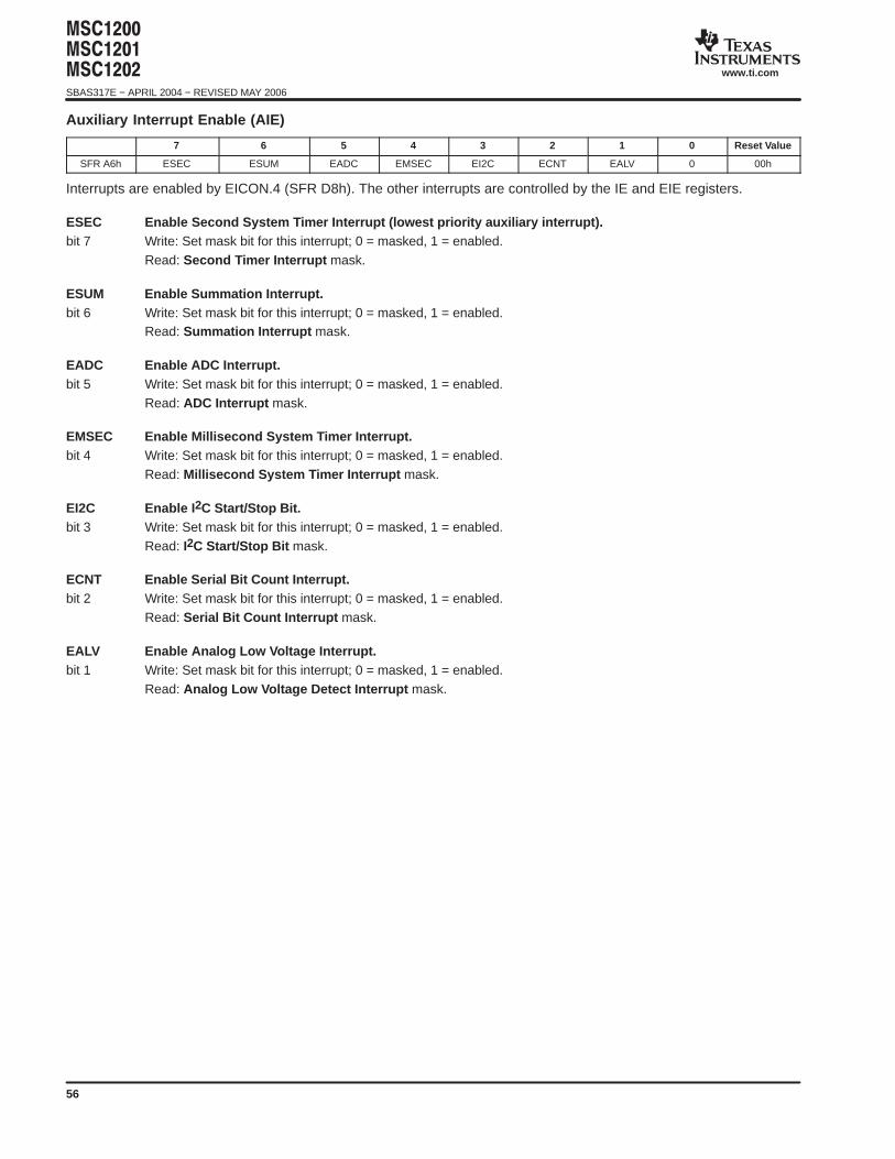
#$#$#$$SBAS317E − APRIL 2004 − REVISED MAY 2006
www.ti.com
56
Auxiliary Interrupt Enable (AIE)
7 6 5 4 3 2 1 0 Reset Value
SFR A6h ESEC ESUM EADC EMSEC EI2C ECNT EALV 0 00h
Interrupts are enabled by EICON.4 (SFR D8h). The other interrupts are controlled by the IE and EIE registers.
ESEC Enable Second System T imer Interrupt (lowest priority auxiliary interrupt).bit 7 Write: Set mask bit for this interrupt; 0 = masked, 1 = enabled.
Read: Second T imer Interrupt mask.
ESUM Enable Summation Interrupt.bit 6 Write: Set mask bit for this interrupt; 0 = masked, 1 = enabled.
Read: Summation Interrupt mask.
EADC Enable ADC Interrupt.bit 5 Write: Set mask bit for this interrupt; 0 = masked, 1 = enabled.
Read: ADC Interrupt mask.
EMSEC Enable Millisecond System Timer Interrupt.bit 4 Write: Set mask bit for this interrupt; 0 = masked, 1 = enabled.
Read: Millisecond System T imer Interrupt mask.
EI2C Enable I 2C Start/Stop Bit.bit 3 Write: Set mask bit for this interrupt; 0 = masked, 1 = enabled.
Read: I2C Start/Stop Bit mask.
ECNT Enable Serial Bit Count Interrupt.bit 2 Write: Set mask bit for this interrupt; 0 = masked, 1 = enabled.
Read: Serial Bit Count Interrupt mask.
EALV Enable Analog Low Voltage Interrupt.bit 1 Write: Set mask bit for this interrupt; 0 = masked, 1 = enabled.
Read: Analog Low Voltage Detect Interrupt mask.
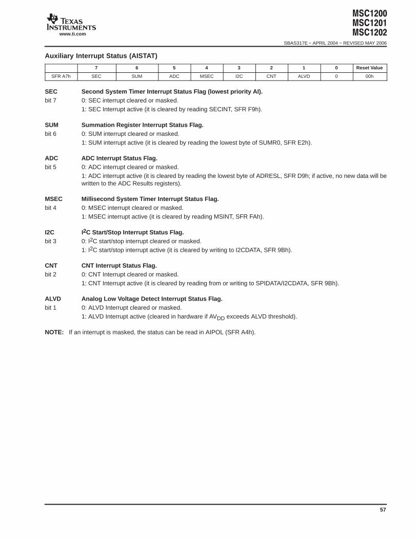
#$#$#$$
SBAS317E − APRIL 2004 − REVISED MAY 2006
www.ti.com
57
Auxiliary Interrupt Status (AISTAT)
7 6 5 4 3 2 1 0 Reset Value
SFR A7h SEC SUM ADC MSEC I2C CNT ALVD 0 00h
SEC Second System Timer Interrupt Status Flag (lowest priority AI).bit 7 0: SEC interrupt cleared or masked.
1: SEC Interrupt active (it is cleared by reading SECINT, SFR F9h).
SUM Summation Register Interrupt Status Flag.bit 6 0: SUM interrupt cleared or masked.
1: SUM interrupt active (it is cleared by reading the lowest byte of SUMR0, SFR E2h).
ADC ADC Interrupt Status Flag.bit 5 0: ADC interrupt cleared or masked.
1: ADC interrupt active (it is cleared by reading the lowest byte of ADRESL, SFR D9h; if active, no new data will bewritten to the ADC Results registers).
MSEC Millisecond System Timer Interrupt Status Flag.bit 4 0: MSEC interrupt cleared or masked.
1: MSEC interrupt active (it is cleared by reading MSINT, SFR FAh).
I2C I2C Start/Stop Interrupt Status Flag.bit 3 0: I2C start/stop interrupt cleared or masked.
1: I2C start/stop interrupt active (it is cleared by writing to I2CDATA, SFR 9Bh).
CNT CNT Interrupt Status Flag.bit 2 0: CNT Interrupt cleared or masked.
1: CNT Interrupt active (it is cleared by reading from or writing to SPIDATA/I2CDATA, SFR 9Bh).
ALVD Analog Low Voltage Detect Interrupt Status Flag.bit 1 0: ALVD Interrupt cleared or masked.
1: ALVD Interrupt active (cleared in hardware if AVDD exceeds ALVD threshold).
NOTE: If an interrupt is masked, the status can be read in AIPOL (SFR A4h).
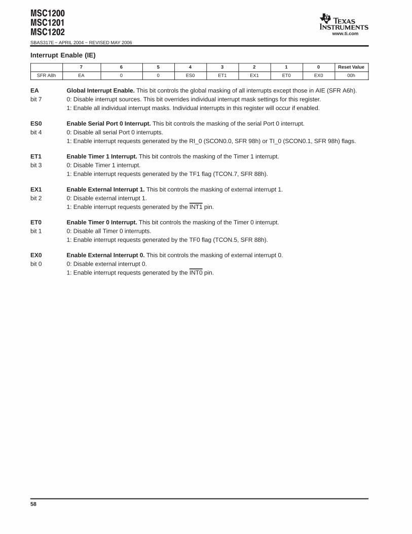
#$#$#$$SBAS317E − APRIL 2004 − REVISED MAY 2006
www.ti.com
58
Interrupt Enable (IE)
7 6 5 4 3 2 1 0 Reset Value
SFR A8h EA 0 0 ES0 ET1 EX1 ET0 EX0 00h
EA Global Interrupt Enable. This bit controls the global masking of all interrupts except those in AIE (SFR A6h).bit 7 0: Disable interrupt sources. This bit overrides individual interrupt mask settings for this register.
1: Enable all individual interrupt masks. Individual interrupts in this register will occur if enabled.
ES0 Enable Serial Port 0 Interrupt. This bit controls the masking of the serial Port 0 interrupt.bit 4 0: Disable all serial Port 0 interrupts.
1: Enable interrupt requests generated by the RI_0 (SCON0.0, SFR 98h) or TI_0 (SCON0.1, SFR 98h) flags.
ET1 Enable T imer 1 Interrupt. This bit controls the masking of the Timer 1 interrupt.bit 3 0: Disable Timer 1 interrupt.
1: Enable interrupt requests generated by the TF1 flag (TCON.7, SFR 88h).
EX1 Enable External Interrupt 1. This bit controls the masking of external interrupt 1.bit 2 0: Disable external interrupt 1.
1: Enable interrupt requests generated by the INT1 pin.
ET0 Enable T imer 0 Interrupt. This bit controls the masking of the Timer 0 interrupt.bit 1 0: Disable all Timer 0 interrupts.
1: Enable interrupt requests generated by the TF0 flag (TCON.5, SFR 88h).
EX0 Enable External Interrupt 0. This bit controls the masking of external interrupt 0.bit 0 0: Disable external interrupt 0.
1: Enable interrupt requests generated by the INT0 pin.
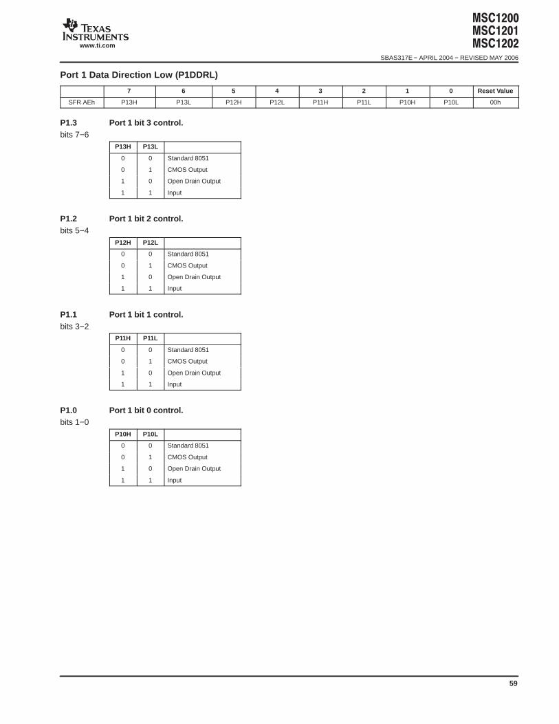
#$#$#$$
SBAS317E − APRIL 2004 − REVISED MAY 2006
www.ti.com
59
Port 1 Data Direction Low (P1DDRL)
7 6 5 4 3 2 1 0 Reset Value
SFR AEh P13H P13L P12H P12L P11H P11L P10H P10L 00h
P1.3 Port 1 bit 3 control.bits 7−6
P13H P13L
0 0 Standard 8051
0 1 CMOS Output
1 0 Open Drain Output
1 1 Input
P1.2 Port 1 bit 2 control.bits 5−4
P12H P12L
0 0 Standard 8051
0 1 CMOS Output
1 0 Open Drain Output
1 1 Input
P1.1 Port 1 bit 1 control.bits 3−2
P11H P11L
0 0 Standard 8051
0 1 CMOS Output
1 0 Open Drain Output
1 1 Input
P1.0 Port 1 bit 0 control.bits 1−0
P10H P10L
0 0 Standard 8051
0 1 CMOS Output
1 0 Open Drain Output
1 1 Input
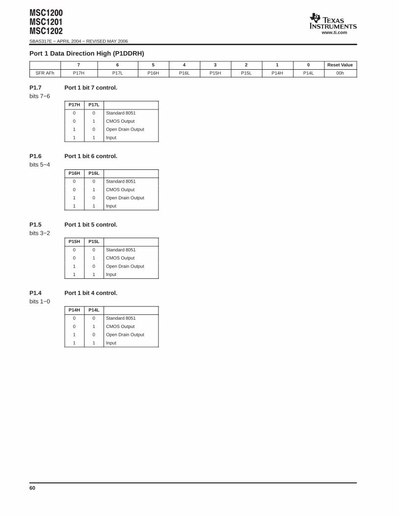
#$#$#$$SBAS317E − APRIL 2004 − REVISED MAY 2006
www.ti.com
60
Port 1 Data Direction High (P1DDRH)
7 6 5 4 3 2 1 0 Reset Value
SFR AFh P17H P17L P16H P16L P15H P15L P14H P14L 00h
P1.7 Port 1 bit 7 control.bits 7−6
P17H P17L
0 0 Standard 8051
0 1 CMOS Output
1 0 Open Drain Output
1 1 Input
P1.6 Port 1 bit 6 control.bits 5−4
P16H P16L
0 0 Standard 8051
0 1 CMOS Output
1 0 Open Drain Output
1 1 Input
P1.5 Port 1 bit 5 control.bits 3−2
P15H P15L
0 0 Standard 8051
0 1 CMOS Output
1 0 Open Drain Output
1 1 Input
P1.4 Port 1 bit 4 control.bits 1−0
P14H P14L
0 0 Standard 8051
0 1 CMOS Output
1 0 Open Drain Output
1 1 Input
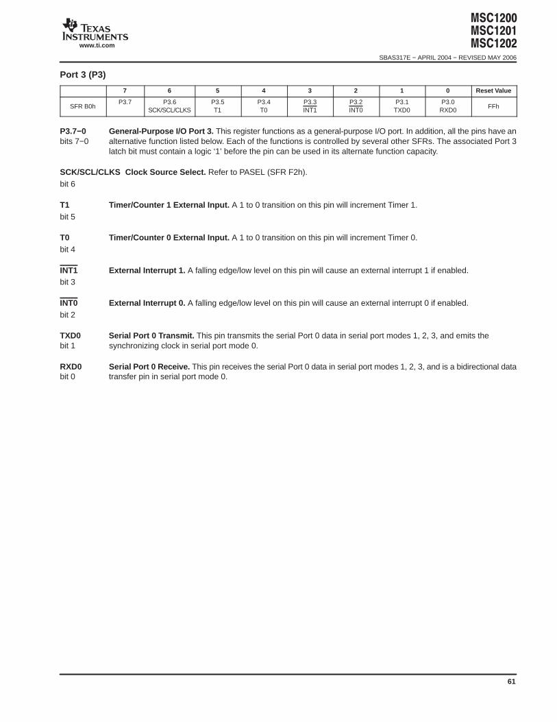
#$#$#$$
SBAS317E − APRIL 2004 − REVISED MAY 2006
www.ti.com
61
Port 3 (P3)
7 6 5 4 3 2 1 0 Reset Value
SFR B0hP3.7 P3.6
SCK/SCL/CLKSP3.5T1
P3.4T0
P3.3INT1
P3.2INT0
P3.1TXD0
P3.0RXD0
FFh
P3.7−0 General-Purpose I/O Port 3. This register functions as a general-purpose I/O port. In addition, all the pins have anbits 7−0 alternative function listed below. Each of the functions is controlled by several other SFRs. The associated Port 3
latch bit must contain a logic ‘1’ before the pin can be used in its alternate function capacity.
SCK/SCL/CLKS Clock So urce Select. Refer to PASEL (SFR F2h).bit 6
T1 Timer/Counter 1 External Input. A 1 to 0 transition on this pin will increment Timer 1.bit 5
T0 Timer/Counter 0 External Input. A 1 to 0 transition on this pin will increment Timer 0.bit 4
INT1 External Interrupt 1. A falling edge/low level on this pin will cause an external interrupt 1 if enabled.bit 3
INT0 External Interrupt 0. A falling edge/low level on this pin will cause an external interrupt 0 if enabled.bit 2
TXD0 Serial Port 0 Transmit. This pin transmits the serial Port 0 data in serial port modes 1, 2, 3, and emits thebit 1 synchronizing clock in serial port mode 0.
RXD0 Serial Port 0 Receive. This pin receives the serial Port 0 data in serial port modes 1, 2, 3, and is a bidirectional databit 0 transfer pin in serial port mode 0.
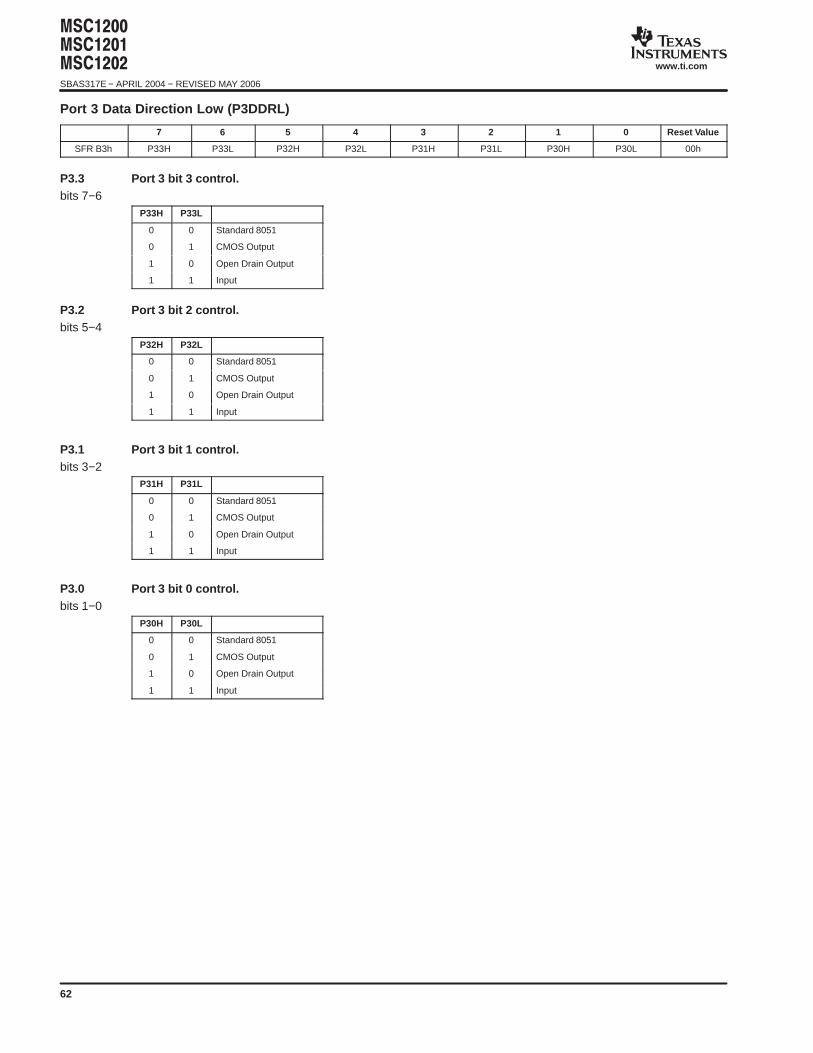
#$#$#$$SBAS317E − APRIL 2004 − REVISED MAY 2006
www.ti.com
62
Port 3 Data Direction Low (P3DDRL)
7 6 5 4 3 2 1 0 Reset Value
SFR B3h P33H P33L P32H P32L P31H P31L P30H P30L 00h
P3.3 Port 3 bit 3 control.bits 7−6
P33H P33L
0 0 Standard 8051
0 1 CMOS Output
1 0 Open Drain Output
1 1 Input
P3.2 Port 3 bit 2 control.bits 5−4
P32H P32L
0 0 Standard 8051
0 1 CMOS Output
1 0 Open Drain Output
1 1 Input
P3.1 Port 3 bit 1 control.bits 3−2
P31H P31L
0 0 Standard 8051
0 1 CMOS Output
1 0 Open Drain Output
1 1 Input
P3.0 Port 3 bit 0 control.bits 1−0
P30H P30L
0 0 Standard 8051
0 1 CMOS Output
1 0 Open Drain Output
1 1 Input
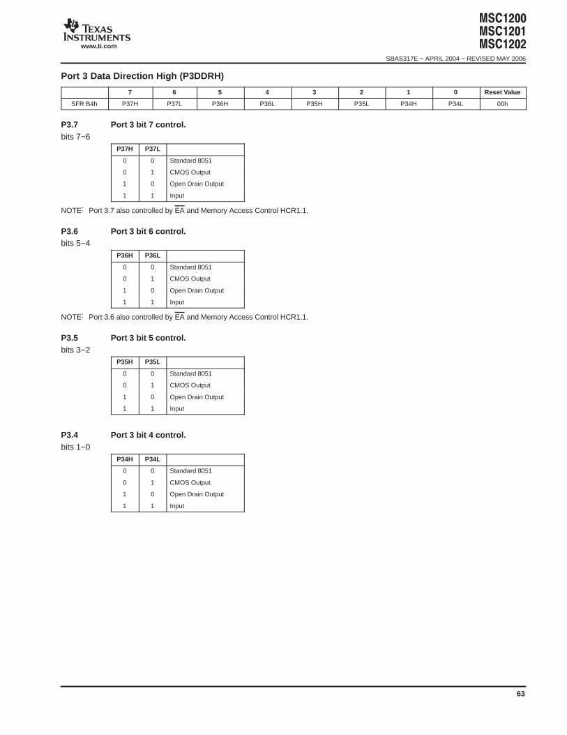
#$#$#$$
SBAS317E − APRIL 2004 − REVISED MAY 2006
www.ti.com
63
Port 3 Data Direction High (P3DDRH)
7 6 5 4 3 2 1 0 Reset Value
SFR B4h P37H P37L P36H P36L P35H P35L P34H P34L 00h
P3.7 Port 3 bit 7 control.bits 7−6
P37H P37L
0 0 Standard 8051
0 1 CMOS Output
1 0 Open Drain Output
1 1 Input
NOTE: Port 3.7 also controlled by EA and Memory Access Control HCR1.1.
P3.6 Port 3 bit 6 control.bits 5−4
P36H P36L
0 0 Standard 8051
0 1 CMOS Output
1 0 Open Drain Output
1 1 Input
NOTE: Port 3.6 also controlled by EA and Memory Access Control HCR1.1.
P3.5 Port 3 bit 5 control.bits 3−2
P35H P35L
0 0 Standard 8051
0 1 CMOS Output
1 0 Open Drain Output
1 1 Input
P3.4 Port 3 bit 4 control.bits 1−0
P34H P34L
0 0 Standard 8051
0 1 CMOS Output
1 0 Open Drain Output
1 1 Input
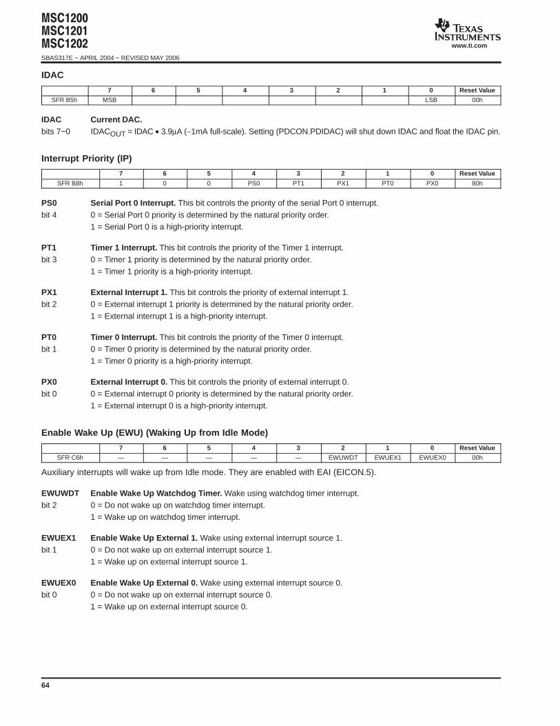
#$#$#$$SBAS317E − APRIL 2004 − REVISED MAY 2006
www.ti.com
64
IDAC
7 6 5 4 3 2 1 0 Reset Value
SFR B5h MSB LSB 00h
IDAC Current DAC.bits 7−0 IDACOUT = IDAC • 3.9µA (∼1mA full-scale). Setting (PDCON.PDIDAC) will shut down IDAC and float the IDAC pin.
Interrupt Priority (IP)
7 6 5 4 3 2 1 0 Reset Value
SFR B8h 1 0 0 PS0 PT1 PX1 PT0 PX0 80h
PS0 Serial Port 0 Interrupt. This bit controls the priority of the serial Port 0 interrupt.bit 4 0 = Serial Port 0 priority is determined by the natural priority order.
1 = Serial Port 0 is a high-priority interrupt.
PT1 Timer 1 Interrupt. This bit controls the priority of the Timer 1 interrupt.bit 3 0 = Timer 1 priority is determined by the natural priority order.
1 = Timer 1 priority is a high-priority interrupt.
PX1 External Interrupt 1. This bit controls the priority of external interrupt 1.bit 2 0 = External interrupt 1 priority is determined by the natural priority order.
1 = External interrupt 1 is a high-priority interrupt.
PT0 Timer 0 Interrupt. This bit controls the priority of the Timer 0 interrupt.bit 1 0 = Timer 0 priority is determined by the natural priority order.
1 = Timer 0 priority is a high-priority interrupt.
PX0 External Interrupt 0. This bit controls the priority of external interrupt 0.bit 0 0 = External interrupt 0 priority is determined by the natural priority order.
1 = External interrupt 0 is a high-priority interrupt.
Enable Wake Up (EWU) (Waking Up from Idle Mode)
7 6 5 4 3 2 1 0 Reset Value
SFR C6h — — — — — EWUWDT EWUEX1 EWUEX0 00h
Auxiliary interrupts will wake up from Idle mode. They are enabled with EAI (EICON.5).
EWUWDT Enable Wake Up Watchdog Timer. Wake using watchdog timer interrupt.bit 2 0 = Do not wake up on watchdog timer interrupt.
1 = Wake up on watchdog timer interrupt.
EWUEX1 Enable Wake Up External 1. Wake using external interrupt source 1.bit 1 0 = Do not wake up on external interrupt source 1.
1 = Wake up on external interrupt source 1.
EWUEX0 Enable Wake Up External 0. Wake using external interrupt source 0.bit 0 0 = Do not wake up on external interrupt source 0.
1 = Wake up on external interrupt source 0.
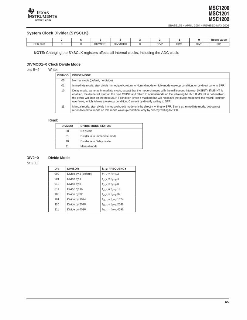
#$#$#$$
SBAS317E − APRIL 2004 − REVISED MAY 2006
www.ti.com
65
System Clock Divider (SYSCLK)
7 6 5 4 3 2 1 0 Reset Value
SFR C7h 0 0 DIVMOD1 DIVMOD0 0 DIV2 DIV1 DIV0 00h
NOTE: Changing the SYSCLK registers affects all internal clocks, including the ADC clock.
DIVMOD1−0 Clock Divide Modebits 5−4 Write:
DIVMOD DIVIDE MODE
00 Normal mode (default, no divide).
01 Immediate mode: start divide immediately; return to Normal mode on Idle mode wakeup condition, or by direct write to SFR.
10 Delay mode: same as Immediate mode, except that the mode changes with the millisecond interrupt (MSINT). If MSINT isenabled, the divide will start on the next MSINT and return to normal mode on the following MSINT. If MSINT is not enabled,the divide will start on the next MSINT condition (even if masked) but will not leave the divide mode until the MSINT counteroverflows, which follows a wakeup condition. Can exit by directly writing to SFR.
11 Manual mode: start divide immediately; exit mode only by directly writing to SFR. Same as immediate mode, but cannotreturn to Normal mode on Idle mode wakeup condition; only by directly writing to SFR.
Read:
DIVMOD DIVIDE MODE STATUS
00 No divide
01 Divider is in Immediate mode
10 Divider is in Delay mode
11 Manual mode
DIV2−0 Divide Modebit 2−0
DIV DIVISOR fCLK FREQUENCY
000 Divide by 2 (default) fCLK = fSYS/2
001 Divide by 4 fCLK = fSYS/4
010 Divide by 8 fCLK = fSYS/8
011 Divide by 16 fCLK = fSYS/16
100 Divide by 32 fCLK = fSYS/32
101 Divide by 1024 fCLK = fSYS/1024
110 Divide by 2048 fCLK = fSYS/2048
111 Divide by 4096 fCLK = fSYS/4096
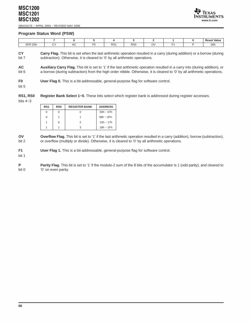
#$#$#$$SBAS317E − APRIL 2004 − REVISED MAY 2006
www.ti.com
66
Program Status Word (PSW)
7 6 5 4 3 2 1 0 Reset Value
SFR D0h CY AC F0 RS1 RS0 OV F1 P 00h
CY Carry Flag. This bit is set when the last arithmetic operation resulted in a carry (during addition) or a borrow (duringbit 7 subtraction). Otherwise, it is cleared to ‘0’ by all arithmetic operations.
AC Auxiliary Carry Flag. This bit is set to ‘1’ if the last arithmetic operation resulted in a carry into (during addition), orbit 6 a borrow (during subtraction) from the high order nibble. Otherwise, it is cleared to ‘0’ by all arithmetic operations.
F0 User Flag 0. This is a bit-addressable, general-purpose flag for software control.bit 5
RS1, RS0 Register Bank Select 1−0. These bits select which register bank is addressed during register accesses.bits 4−3
RS1 RS0 REGISTER BANK ADDRESS
0 0 0 00h − 07h
0 1 1 08h − 0Fh
1 0 2 10h − 17h
1 1 3 18h − 1Fh
OV Overflow Flag. This bit is set to ‘1’ if the last arithmetic operation resulted in a carry (addition), borrow (subtraction),bit 2 or overflow (multiply or divide). Otherwise, it is cleared to ‘0’ by all arithmetic operations.
F1 User Flag 1. This is a bit-addressable, general-purpose flag for software control.bit 1
P Parity Flag. This bit is set to ‘1’ if the modulo-2 sum of the 8 bits of the accumulator is 1 (odd parity), and cleared tobit 0 ‘0’ on even parity.
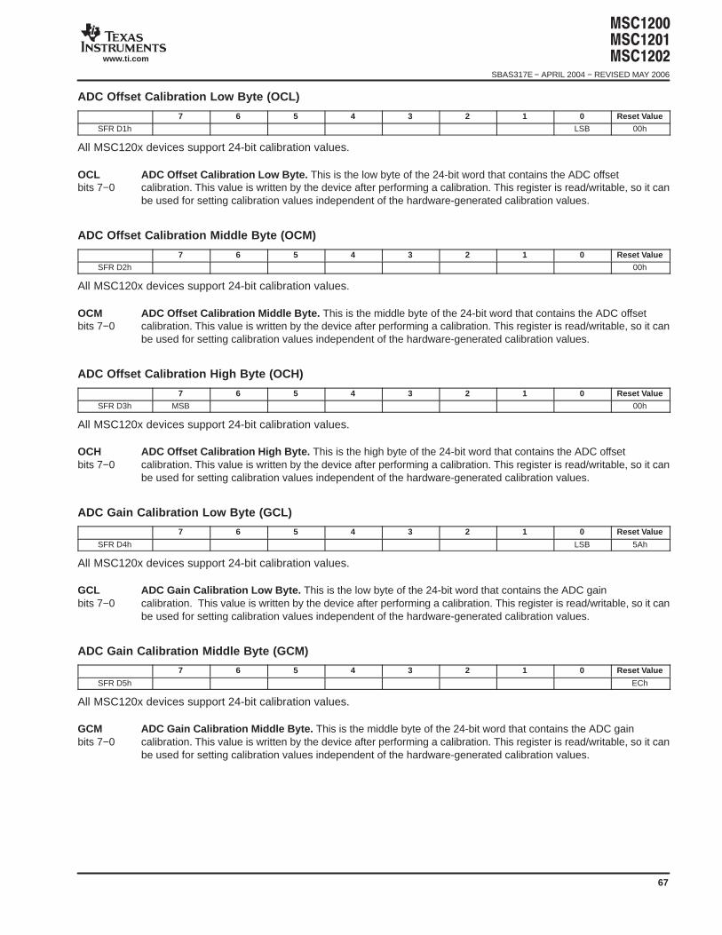
#$#$#$$
SBAS317E − APRIL 2004 − REVISED MAY 2006
www.ti.com
67
ADC Offset Calibration Low Byte (OCL)
7 6 5 4 3 2 1 0 Reset Value
SFR D1h LSB 00h
All MSC120x devices support 24-bit calibration values.
OCL ADC Offset Calibration Low Byte. This is the low byte of the 24-bit word that contains the ADC offsetbits 7−0 calibration. This value is written by the device after performing a calibration. This register is read/writable, so it can
be used for setting calibration values independent of the hardware-generated calibration values.
ADC Offset Calibration Middle Byte (OCM)
7 6 5 4 3 2 1 0 Reset Value
SFR D2h 00h
All MSC120x devices support 24-bit calibration values.
OCM ADC Offset Calibration Middle Byte. This is the middle byte of the 24-bit word that contains the ADC offsetbits 7−0 calibration. This value is written by the device after performing a calibration. This register is read/writable, so it can
be used for setting calibration values independent of the hardware-generated calibration values.
ADC Offset Calibration High Byte (OCH)
7 6 5 4 3 2 1 0 Reset Value
SFR D3h MSB 00h
All MSC120x devices support 24-bit calibration values.
OCH ADC Offset Calibration High Byte. This is the high byte of the 24-bit word that contains the ADC offsetbits 7−0 calibration. This value is written by the device after performing a calibration. This register is read/writable, so it can
be used for setting calibration values independent of the hardware-generated calibration values.
ADC Gain Calibration Low Byte (GCL)
7 6 5 4 3 2 1 0 Reset Value
SFR D4h LSB 5Ah
All MSC120x devices support 24-bit calibration values.
GCL ADC Gain Calibration Low Byte. This is the low byte of the 24-bit word that contains the ADC gainbits 7−0 calibration. This value is written by the device after performing a calibration. This register is read/writable, so it can
be used for setting calibration values independent of the hardware-generated calibration values.
ADC Gain Calibration Middle Byte (GCM)
7 6 5 4 3 2 1 0 Reset Value
SFR D5h ECh
All MSC120x devices support 24-bit calibration values.
GCM ADC Gain Calibration Middle Byte. This is the middle byte of the 24-bit word that contains the ADC gainbits 7−0 calibration. This value is written by the device after performing a calibration. This register is read/writable, so it can
be used for setting calibration values independent of the hardware-generated calibration values.
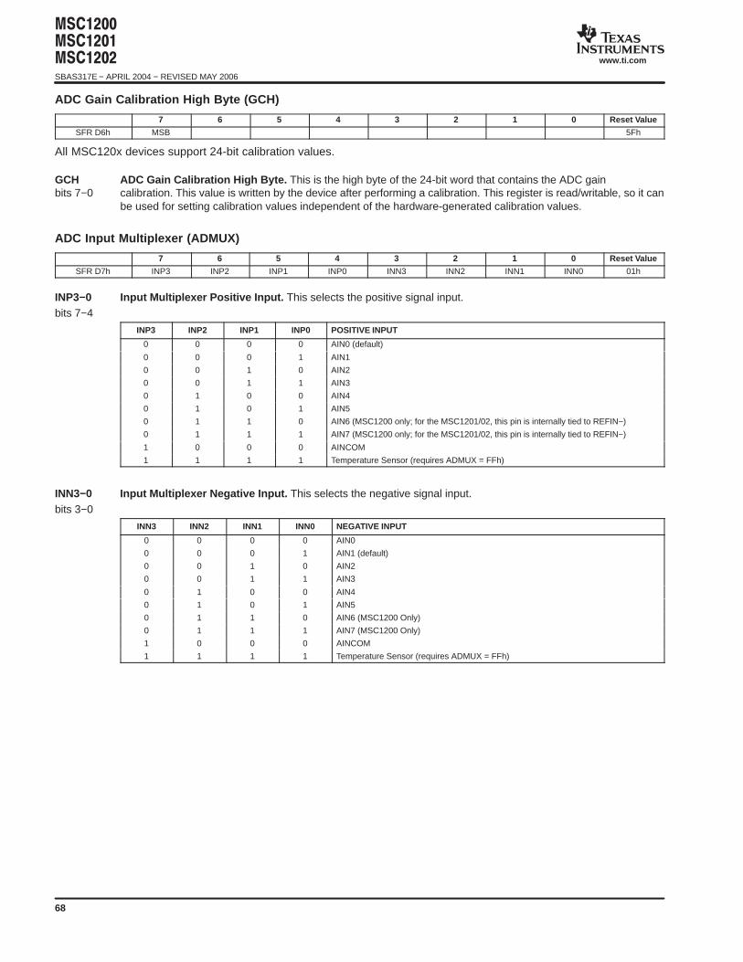
#$#$#$$SBAS317E − APRIL 2004 − REVISED MAY 2006
www.ti.com
68
ADC Gain Calibration High Byte (GCH)
7 6 5 4 3 2 1 0 Reset Value
SFR D6h MSB 5Fh
All MSC120x devices support 24-bit calibration values.
GCH ADC Gain Calibration High Byte. This is the high byte of the 24-bit word that contains the ADC gainbits 7−0 calibration. This value is written by the device after performing a calibration. This register is read/writable, so it can
be used for setting calibration values independent of the hardware-generated calibration values.
ADC Input Multiplexer (ADMUX)
7 6 5 4 3 2 1 0 Reset Value
SFR D7h INP3 INP2 INP1 INP0 INN3 INN2 INN1 INN0 01h
INP3−0 Input Multiplexer Positive Input. This selects the positive signal input.bits 7−4
INP3 INP2 INP1 INP0 POSITIVE INPUT
0 0 0 0 AIN0 (default)
0 0 0 1 AIN1
0 0 1 0 AIN2
0 0 1 1 AIN3
0 1 0 0 AIN4
0 1 0 1 AIN5
0 1 1 0 AIN6 (MSC1200 only; for the MSC1201/02, this pin is internally tied to REFIN−)
0 1 1 1 AIN7 (MSC1200 only; for the MSC1201/02, this pin is internally tied to REFIN−)
1 0 0 0 AINCOM
1 1 1 1 Temperature Sensor (requires ADMUX = FFh)
INN3−0 Input Multiplexer Negative Input. This selects the negative signal input.bits 3−0
INN3 INN2 INN1 INN0 NEGATIVE INPUT
0 0 0 0 AIN0
0 0 0 1 AIN1 (default)
0 0 1 0 AIN2
0 0 1 1 AIN3
0 1 0 0 AIN4
0 1 0 1 AIN5
0 1 1 0 AIN6 (MSC1200 Only)
0 1 1 1 AIN7 (MSC1200 Only)
1 0 0 0 AINCOM
1 1 1 1 Temperature Sensor (requires ADMUX = FFh)
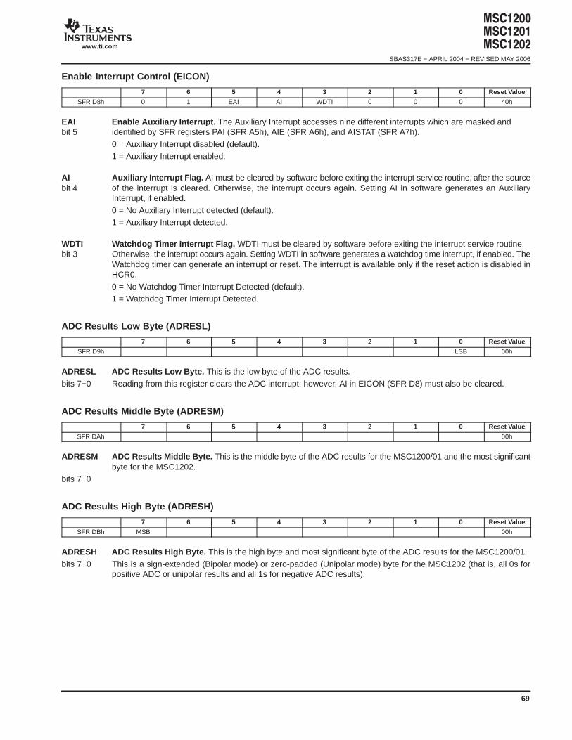
#$#$#$$
SBAS317E − APRIL 2004 − REVISED MAY 2006
www.ti.com
69
Enable Interrupt Control (EICON)
7 6 5 4 3 2 1 0 Reset Value
SFR D8h 0 1 EAI AI WDTI 0 0 0 40h
EAI Enable Auxiliary Interrupt. The Auxiliary Interrupt accesses nine different interrupts which are masked andbit 5 identified by SFR registers PAI (SFR A5h), AIE (SFR A6h), and AISTAT (SFR A7h).
0 = Auxiliary Interrupt disabled (default).1 = Auxiliary Interrupt enabled.
AI Auxiliary Interrupt Flag. AI must be cleared by software before exiting the interrupt service routine, after the sourcebit 4 of the interrupt is cleared. Otherwise, the interrupt occurs again. Setting AI in software generates an Auxiliary
Interrupt, if enabled.0 = No Auxiliary Interrupt detected (default).1 = Auxiliary Interrupt detected.
WDTI Watchdog T imer Interrupt Flag. WDTI must be cleared by software before exiting the interrupt service routine.bit 3 Otherwise, the interrupt occurs again. Setting WDTI in software generates a watchdog time interrupt, if enabled. The
Watchdog timer can generate an interrupt or reset. The interrupt is available only if the reset action is disabled inHCR0.0 = No Watchdog Timer Interrupt Detected (default).1 = Watchdog Timer Interrupt Detected.
ADC Results Low Byte (ADRESL)
7 6 5 4 3 2 1 0 Reset Value
SFR D9h LSB 00h
ADRESL ADC Results Low Byte. This is the low byte of the ADC results.bits 7−0 Reading from this register clears the ADC interrupt; however, AI in EICON (SFR D8) must also be cleared.
ADC Results Middle Byte (ADRESM)
7 6 5 4 3 2 1 0 Reset Value
SFR DAh 00h
ADRESM ADC Results Middle Byte. This is the middle byte of the ADC results for the MSC1200/01 and the most significantbyte for the MSC1202.
bits 7−0
ADC Results High Byte (ADRESH)
7 6 5 4 3 2 1 0 Reset Value
SFR DBh MSB 00h
ADRESH ADC Results High Byte. This is the high byte and most significant byte of the ADC results for the MSC1200/01.bits 7−0 This is a sign-extended (Bipolar mode) or zero-padded (Unipolar mode) byte for the MSC1202 (that is, all 0s for
positive ADC or unipolar results and all 1s for negative ADC results).
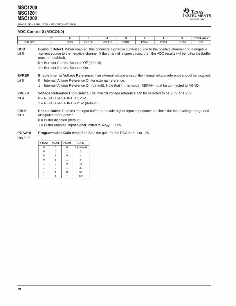
#$#$#$$SBAS317E − APRIL 2004 − REVISED MAY 2006
www.ti.com
70
ADC Control 0 (ADCON0)
7 6 5 4 3 2 1 0 Reset Value
SFR DCh — BOD EVREF VREFH EBUF PGA2 PGA1 PGA0 30h
BOD Burnout Detect. When enabled, this connects a positive current source to the positive channel and a negativebit 6 current source to the negative channel. If the channel is open circuit, then the ADC results will be full-scale (buffer
must be enabled).0 = Burnout Current Sources Off (default).1 = Burnout Current Sources On.
EVREF Enable Internal V oltage Reference. If an external voltage is used, the internal voltage reference should be disabled.bit 5 0 = Internal Voltage Reference Off for external reference.
1 = Internal Voltage Reference On (default). Note that in this mode, REFIN− must be connected to AGND.
VREFH Voltage Reference High Select. The internal voltage reference can be selected to be 2.5V or 1.25V.bit 4 0 = REFOUT/REF IN+ is 1.25V.
1 = REFOUT/REF IN+ is 2.5V (default).
EBUF Enable Buffer. Enables the input buffer to provide higher input impedance but limits the input voltage range andbit 3 dissipates more power.
0 = Buffer disabled (default).1 = Buffer enabled. Input signal limited to AVDD − 1.5V.
PGA2−0 Programmable Gain Amplifier. Sets the gain for the PGA from 1 to 128.bits 2−0
PGA2 PGA1 PGA0 GAIN
0 0 0 1 (default)
0 0 1 2
0 1 0 4
0 1 1 8
1 0 0 16
1 0 1 32
1 1 0 64
1 1 1 128
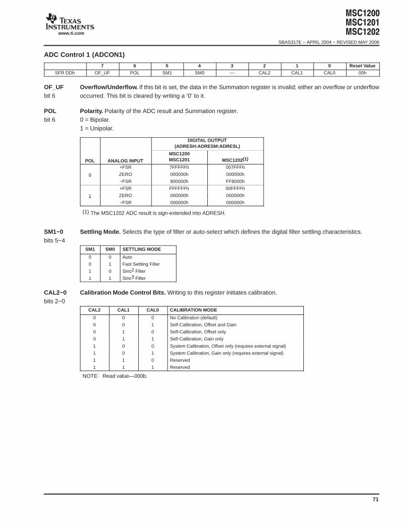
#$#$#$$
SBAS317E − APRIL 2004 − REVISED MAY 2006
www.ti.com
71
ADC Control 1 (ADCON1)
7 6 5 4 3 2 1 0 Reset Value
SFR DDh OF_UF POL SM1 SM0 — CAL2 CAL1 CAL0 00h
OF_UF Overflow/Underflow. If this bit is set, the data in the Summation register is invalid; either an overflow or underflowbit 6 occurred. This bit is cleared by writing a ‘0’ to it.
POL Polarity. Polarity of the ADC result and Summation register.bit 6 0 = Bipolar.
1 = Unipolar.
DIGITAL OUTPUT(ADRESH:ADRESM:ADRESL)
POL ANALOG INPUT
MSC1200MSC1201 MSC1202(1)
+FSR 7FFFFFh 007FFFh
0 ZERO 000000h 000000h0−FSR 800000h FF8000h
+FSR FFFFFFh 00FFFFh
1 ZERO 000000h 000000h1−FSR 000000h 000000h
(1) The MSC1202 ADC result is sign-extended into ADRESH.
SM1−0 Settling Mode. Selects the type of filter or auto-select which defines the digital filter settling characteristics.bits 5−4
SM1 SM0 SETTLING MODE
0 0 Auto
0 1 Fast Settling Filter
1 0 Sinc2 Filter
1 1 Sinc3 Filter
CAL2−0 Calibration Mode Control Bits. Writing to this register initiates calibration.bits 2−0
CAL2 CAL1 CAL0 CALIBRATION MODE
0 0 0 No Calibration (default)
0 0 1 Self-Calibration, Offset and Gain
0 1 0 Self-Calibration, Offset only
0 1 1 Self-Calibration, Gain only
1 0 0 System Calibration, Offset only (requires external signal)
1 0 1 System Calibration, Gain only (requires external signal)
1 1 0 Reserved
1 1 1 Reserved
NOTE: Read value—000b.
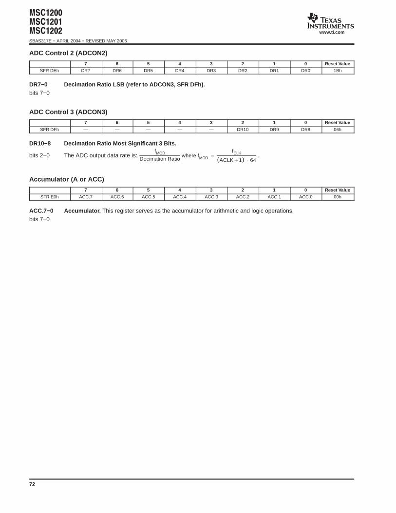
#$#$#$$SBAS317E − APRIL 2004 − REVISED MAY 2006
www.ti.com
72
ADC Control 2 (ADCON2)
7 6 5 4 3 2 1 0 Reset Value
SFR DEh DR7 DR6 DR5 DR4 DR3 DR2 DR1 DR0 1Bh
DR7−0 Decimation Ratio LSB (refer to ADCON3, SFR DFh).bits 7−0
ADC Control 3 (ADCON3)
7 6 5 4 3 2 1 0 Reset Value
SFR DFh — — — — — DR10 DR9 DR8 06h
DR10−8 Decimation Ratio Most Significant 3 Bits.
bits 2−0 The ADC output data rate is: fMOD
Decimation Ratiowhere fMOD
fCLK
ACLK1 64 .
Accumulator (A or ACC)
7 6 5 4 3 2 1 0 Reset Value
SFR E0h ACC.7 ACC.6 ACC.5 ACC.4 ACC.3 ACC.2 ACC.1 ACC.0 00h
ACC.7−0 Accumulator. This register serves as the accumulator for arithmetic and logic operations.bits 7−0
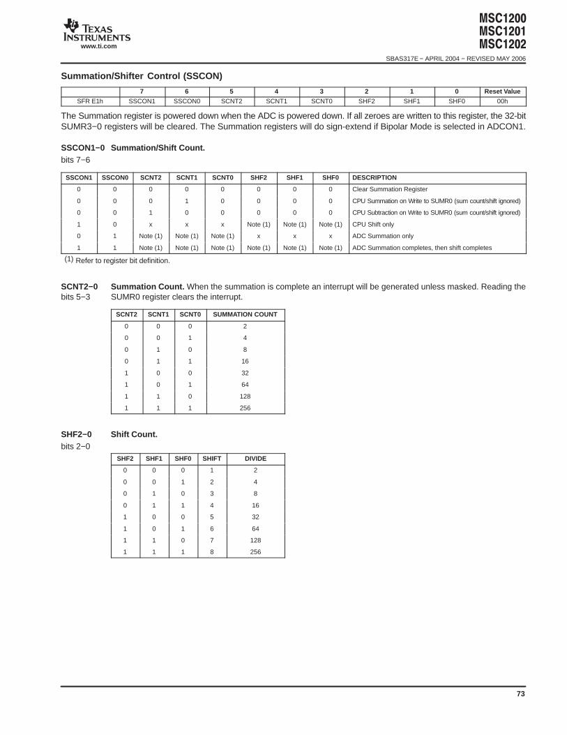
#$#$#$$
SBAS317E − APRIL 2004 − REVISED MAY 2006
www.ti.com
73
Summation/Shifter Control (SSCON)
7 6 5 4 3 2 1 0 Reset Value
SFR E1h SSCON1 SSCON0 SCNT2 SCNT1 SCNT0 SHF2 SHF1 SHF0 00h
The Summation register is powered down when the ADC is powered down. If all zeroes are written to this register, the 32-bitSUMR3−0 registers will be cleared. The Summation registers will do sign-extend if Bipolar Mode is selected in ADCON1.
SSCON1−0 Summation/Shift Count.bits 7−6
SSCON1 SSCON0 SCNT2 SCNT1 SCNT0 SHF2 SHF1 SHF0 DESCRIPTION
0 0 0 0 0 0 0 0 Clear Summation Register
0 0 0 1 0 0 0 0 CPU Summation on Write to SUMR0 (sum count/shift ignored)
0 0 1 0 0 0 0 0 CPU Subtraction on Write to SUMR0 (sum count/shift ignored)
1 0 x x x Note (1) Note (1) Note (1) CPU Shift only
0 1 Note (1) Note (1) Note (1) x x x ADC Summation only
1 1 Note (1) Note (1) Note (1) Note (1) Note (1) Note (1) ADC Summation completes, then shift completes
(1) Refer to register bit definition.
SCNT2−0 Summation Count. When the summation is complete an interrupt will be generated unless masked. Reading thebits 5−3 SUMR0 register clears the interrupt.
SCNT2 SCNT1 SCNT0 SUMMATION COUNT
0 0 0 2
0 0 1 4
0 1 0 8
0 1 1 16
1 0 0 32
1 0 1 64
1 1 0 128
1 1 1 256
SHF2−0 Shift Count.bits 2−0
SHF2 SHF1 SHF0 SHIFT DIVIDE
0 0 0 1 2
0 0 1 2 4
0 1 0 3 8
0 1 1 4 16
1 0 0 5 32
1 0 1 6 64
1 1 0 7 128
1 1 1 8 256
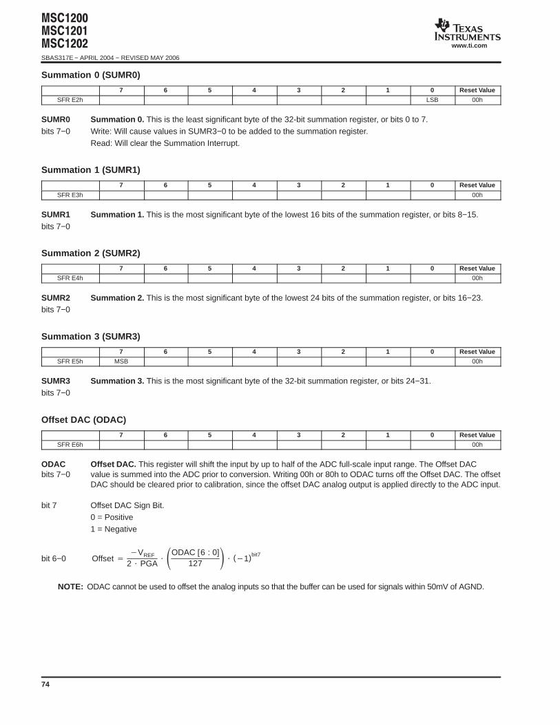
#$#$#$$SBAS317E − APRIL 2004 − REVISED MAY 2006
www.ti.com
74
Summation 0 (SUMR0)
7 6 5 4 3 2 1 0 Reset Value
SFR E2h LSB 00h
SUMR0 Summation 0. This is the least significant byte of the 32-bit summation register, or bits 0 to 7.bits 7−0 Write: Will cause values in SUMR3−0 to be added to the summation register.
Read: Will clear the Summation Interrupt.
Summation 1 (SUMR1)
7 6 5 4 3 2 1 0 Reset Value
SFR E3h 00h
SUMR1 Summation 1. This is the most significant byte of the lowest 16 bits of the summation register, or bits 8−15.bits 7−0
Summation 2 (SUMR2)
7 6 5 4 3 2 1 0 Reset Value
SFR E4h 00h
SUMR2 Summation 2. This is the most significant byte of the lowest 24 bits of the summation register, or bits 16−23.bits 7−0
Summation 3 (SUMR3)
7 6 5 4 3 2 1 0 Reset Value
SFR E5h MSB 00h
SUMR3 Summation 3. This is the most significant byte of the 32-bit summation register, or bits 24−31.bits 7−0
Offset DAC (ODAC)
7 6 5 4 3 2 1 0 Reset Value
SFR E6h 00h
ODAC Offset DAC. This register will shift the input by up to half of the ADC full-scale input range. The Offset DACbits 7−0 value is summed into the ADC prior to conversion. Writing 00h or 80h to ODAC turns off the Offset DAC. The offset
DAC should be cleared prior to calibration, since the offset DAC analog output is applied directly to the ADC input.
bit 7 Offset DAC Sign Bit.0 = Positive1 = Negative
bit 6−0 Offset VREF
2 PGA ODAC [6 : 0]
127 (1)bit7
NOTE: ODAC cannot be used to offset the analog inputs so that the buffer can be used for signals within 50mV of AGND.
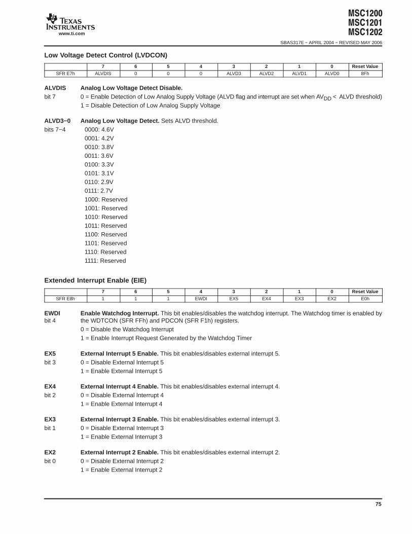
#$#$#$$
SBAS317E − APRIL 2004 − REVISED MAY 2006
www.ti.com
75
Low Voltage Detect Control (LVDCON)
7 6 5 4 3 2 1 0 Reset Value
SFR E7h ALVDIS 0 0 0 ALVD3 ALVD2 ALVD1 ALVD0 8Fh
ALVDIS Analog Low Voltage Detect Disable.bit 7 0 = Enable Detection of Low Analog Supply Voltage (ALVD flag and interrupt are set when AVDD < ALVD threshold)
1 = Disable Detection of Low Analog Supply Voltage
ALVD3−0 Analog Low Voltage Detect. Sets ALVD threshold.bits 7−4 0000: 4.6V
0001: 4.2V0010: 3.8V0011: 3.6V0100: 3.3V0101: 3.1V0110: 2.9V0111: 2.7V1000: Reserved1001: Reserved1010: Reserved1011: Reserved1100: Reserved1101: Reserved1110: Reserved1111: Reserved
Extended Interrupt Enable (EIE)
7 6 5 4 3 2 1 0 Reset Value
SFR E8h 1 1 1 EWDI EX5 EX4 EX3 EX2 E0h
EWDI Enable Watchdog Interrupt. This bit enables/disables the watchdog interrupt. The Watchdog timer is enabled bybit 4 the WDTCON (SFR FFh) and PDCON (SFR F1h) registers.
0 = Disable the Watchdog Interrupt1 = Enable Interrupt Request Generated by the Watchdog Timer
EX5 External Interrupt 5 Enable. This bit enables/disables external interrupt 5.bit 3 0 = Disable External Interrupt 5
1 = Enable External Interrupt 5
EX4 External Interrupt 4 Enable. This bit enables/disables external interrupt 4.bit 2 0 = Disable External Interrupt 4
1 = Enable External Interrupt 4
EX3 External Interrupt 3 Enable. This bit enables/disables external interrupt 3.bit 1 0 = Disable External Interrupt 3
1 = Enable External Interrupt 3
EX2 External Interrupt 2 Enable. This bit enables/disables external interrupt 2.bit 0 0 = Disable External Interrupt 2
1 = Enable External Interrupt 2
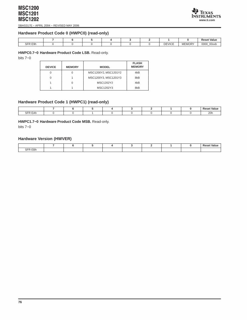
#$#$#$$SBAS317E − APRIL 2004 − REVISED MAY 2006
www.ti.com
76
Hardware Product Code 0 (HWPC0) (read-only)
7 6 5 4 3 2 1 0 Reset Value
SFR E9h 0 0 0 0 0 0 DEVICE MEMORY 0000_00xxb
HWPC0.7−0 Hardware Product Code LSB. Read-only.bits 7−0
DEVICE MEMORY MODELFLASH
MEMORY
0 0 MSC1200Y2, MSC1201Y2 4kB
0 1 MSC1200Y3, MSC1201Y3 8kB
1 0 MSC1202Y2 4kB
1 1 MSC1202Y3 8kB
Hardware Product Code 1 (HWPC1) (read-only)
7 6 5 4 3 2 1 0 Reset Value
SFR EAh 0 0 1 0 0 0 0 0 20h
HWPC1.7−0 Hardware Product Code MSB. Read-only.bits 7−0
Hardware Version (HWVER)
7 6 5 4 3 2 1 0 Reset Value
SFR EBh
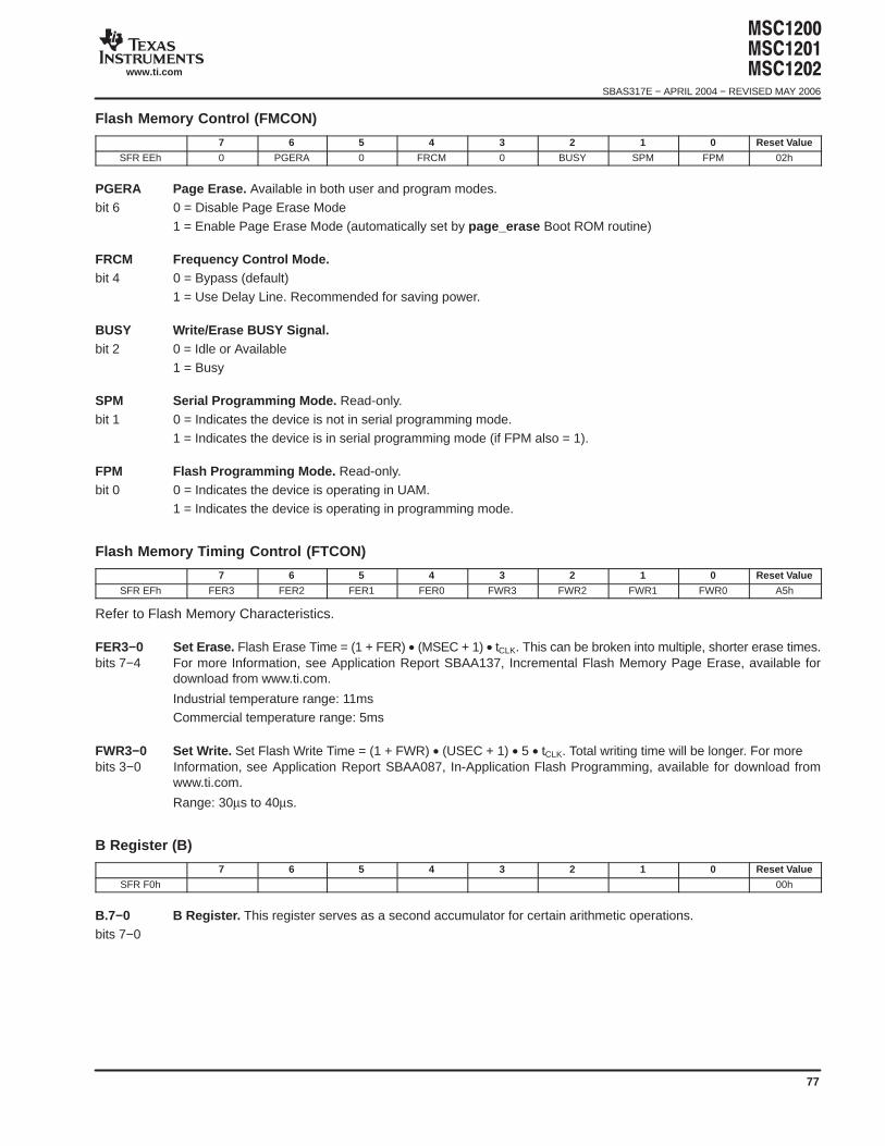
#$#$#$$
SBAS317E − APRIL 2004 − REVISED MAY 2006
www.ti.com
77
Flash Memory Control (FMCON)
7 6 5 4 3 2 1 0 Reset Value
SFR EEh 0 PGERA 0 FRCM 0 BUSY SPM FPM 02h
PGERA Page Erase. Available in both user and program modes.bit 6 0 = Disable Page Erase Mode
1 = Enable Page Erase Mode (automatically set by page_erase Boot ROM routine)
FRCM Frequency Control Mode.bit 4 0 = Bypass (default)
1 = Use Delay Line. Recommended for saving power.
BUSY Write/Erase BUSY Signal.bit 2 0 = Idle or Available
1 = Busy
SPM Serial Programming Mode. Read-only.bit 1 0 = Indicates the device is not in serial programming mode.
1 = Indicates the device is in serial programming mode (if FPM also = 1).
FPM Flash Programming Mode. Read-only.bit 0 0 = Indicates the device is operating in UAM.
1 = Indicates the device is operating in programming mode.
Flash Memory Timing Control (FTCON)
7 6 5 4 3 2 1 0 Reset Value
SFR EFh FER3 FER2 FER1 FER0 FWR3 FWR2 FWR1 FWR0 A5h
Refer to Flash Memory Characteristics.
FER3−0 Set Erase. Flash Erase Time = (1 + FER) • (MSEC + 1) • tCLK. This can be broken into multiple, shorter erase times.bits 7−4 For more Information, see Application Report SBAA137, Incremental Flash Memory Page Erase, available for
download from www.ti.com.
Industrial temperature range: 11msCommercial temperature range: 5ms
FWR3−0 Set Write. Set Flash Write Time = (1 + FWR) • (USEC + 1) • 5 • tCLK. Total writing time will be longer. For morebits 3−0 Information, see Application Report SBAA087, In-Application Flash Programming, available for download from
www.ti.com.
Range: 30µs to 40µs.
B Register (B)
7 6 5 4 3 2 1 0 Reset Value
SFR F0h 00h
B.7−0 B Register. This register serves as a second accumulator for certain arithmetic operations.bits 7−0
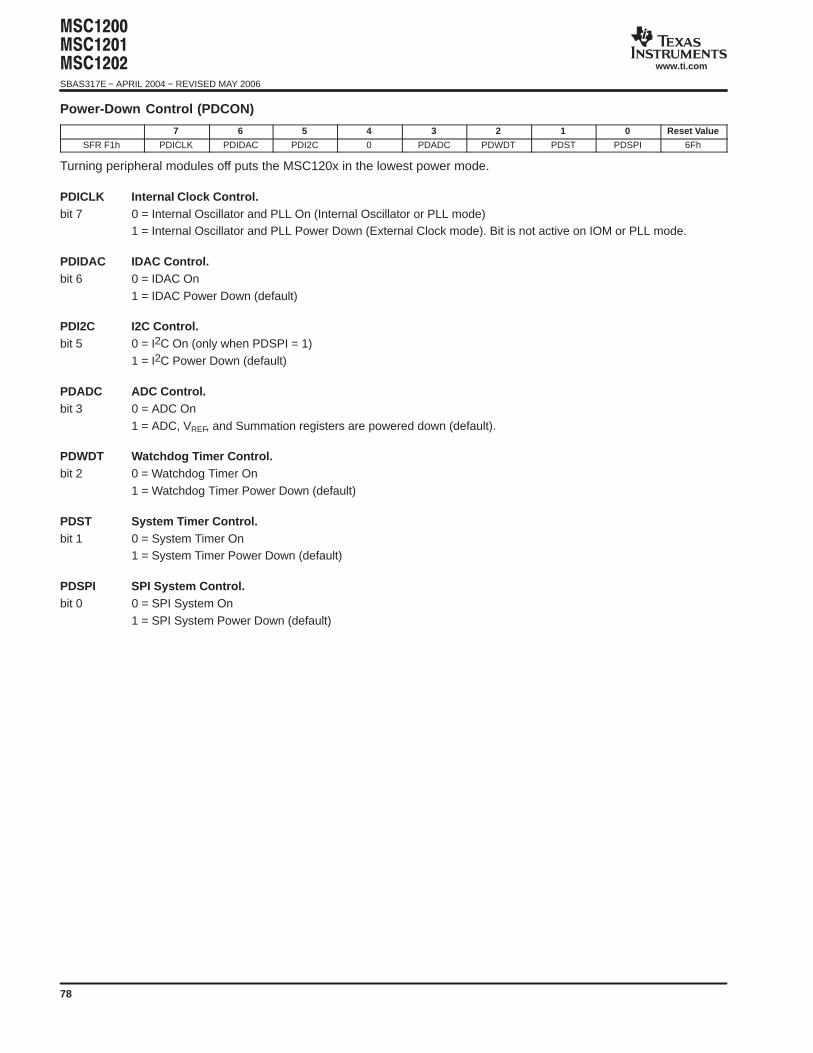
#$#$#$$SBAS317E − APRIL 2004 − REVISED MAY 2006
www.ti.com
78
Power-Down Control (PDCON)
7 6 5 4 3 2 1 0 Reset Value
SFR F1h PDICLK PDIDAC PDI2C 0 PDADC PDWDT PDST PDSPI 6Fh
Turning peripheral modules off puts the MSC120x in the lowest power mode.
PDICLK Internal Clock Control.bit 7 0 = Internal Oscillator and PLL On (Internal Oscillator or PLL mode)
1 = Internal Oscillator and PLL Power Down (External Clock mode). Bit is not active on IOM or PLL mode.
PDIDAC IDAC Control.bit 6 0 = IDAC On
1 = IDAC Power Down (default)
PDI2C I2C Control.bit 5 0 = I2C On (only when PDSPI = 1)
1 = I2C Power Down (default)
PDADC ADC Control.bit 3 0 = ADC On
1 = ADC, VREF, and Summation registers are powered down (default).
PDWDT Watchdog Timer Control.bit 2 0 = Watchdog Timer On
1 = Watchdog Timer Power Down (default)
PDST System Timer Control.bit 1 0 = System Timer On
1 = System Timer Power Down (default)
PDSPI SPI System Control.bit 0 0 = SPI System On
1 = SPI System Power Down (default)
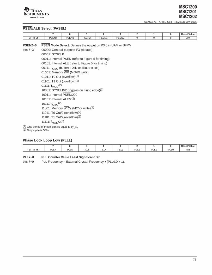
#$#$#$$
SBAS317E − APRIL 2004 − REVISED MAY 2006
www.ti.com
79
PSEN/ALE Select (PASEL)
7 6 5 4 3 2 1 0 Reset Value
SFR F2h PSEN4 PSEN3 PSEN2 PSEN1 PSEN0 0 0 0 00h
PSEN2−0 PSEN Mode Select. Defines the output on P3.6 in UAM or SFPM.bits 7−3 00000: General-purpose I/O (default)
00001: SYSCLK00011: Internal PSEN (refer to Figure 5 for timing)00101: Internal ALE (refer to Figure 5 for timing)00111: fOSC (buffered XIN oscillator clock)01001: Memory WR (MOVX write)01011: T0 Out (overflow)(1)
01101: T1 Out (overflow)(1)
01111: fMOD(2)
10001: SYSCLK/2 (toggles on rising edge)(2)
10011: Internal PSEN/2(2)
10101: Internal ALE/2(2)
10111: fOSC(2)
11001: Memory WR/2 (MOVX write)(2)
11011: T0 Out/2 (overflow)(2)
11101: T1 Out/2 (overflow)(2)
11111: fMOD/2(2)
(1) One period of these signals equal to tCLK.(2) Duty cycle is 50%.
Phase Lock Loop Low (PLLL)
7 6 5 4 3 2 1 0 Reset Value
SFR F4h PLL7 PLL6 PLL5 PLL4 PLL3 PLL2 PLL1 PLL0 xxh
PLL7−0 PLL Counter V alue Least Significant Bit.bits 7−0 PLL Frequency = External Crystal Frequency • (PLL9:0 + 1).
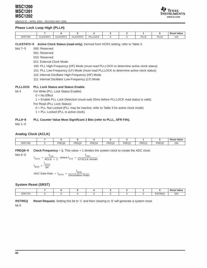
#$#$#$$SBAS317E − APRIL 2004 − REVISED MAY 2006
www.ti.com
80
Phase Lock Loop High (PLLH)
7 6 5 4 3 2 1 0 Reset Value
SFR F5h CLKSTAT2 CLKSTAT1 CLKSTAT0 PLLLOCK 0 0 PLL9 PLL8 xxh
CLKSTAT2−0 Active Clock Status (read-only). Derived from HCR2 setting; refer to Table 3.bits 7−5 000: Reserved
001: Reserved010: Reserved011: External Clock Mode100: PLL High-Frequency (HF) Mode (must read PLLLOCK to determine active clock status)101: PLL Low-Frequency (LF) Mode (must read PLLLOCK to determine active clock status)110: Internal Oscillator High-Frequency (HF) Mode111: Internal Oscillator Low-Frequency (LF) Mode
PLLLOCK PLL Lock Status and Status Enable.bit 4 For Write (PLL Lock Status Enable):
0 = No Effect1 = Enable PLL Lock Detection (must wait 20ms before PLLLOCK read status is valid).
For Read (PLL Lock Status):0 = PLL Not Locked (PLL may be inactive; refer to Table 3 for active clock mode)1 = PLL Locked (PLL is active clock).
PLL9−8 PLL Counter Value Most Significant 2 Bits (refer to PLLL, SFR F4h).bits 1−0
Analog Clock (ACLK)
7 6 5 4 3 2 1 0 Reset Value
SFR F6h 0 FREQ6 FREQ5 FREQ4 FREQ3 FREQ2 FREQ1 FREQ0 03h
FREQ6−0 Clock Frequency − 1. This value + 1 divides the system clock to create the ADC clock.bits 6−0
fACLK fCLK
ACLK 1, where fCLK
fOSC
SYSCLK divider
.
fMOD fACLK
64
ADC Data Rate fDATA fMOD
Decimation Ratio
System Reset (SRST)
7 6 5 4 3 2 1 0 Reset Value
SFR F7h 0 0 0 0 0 0 0 RSTREQ 00h
RSTREQ Reset Request. Setting this bit to ‘1’ and then clearing to ‘0’ will generate a system reset.bit 0
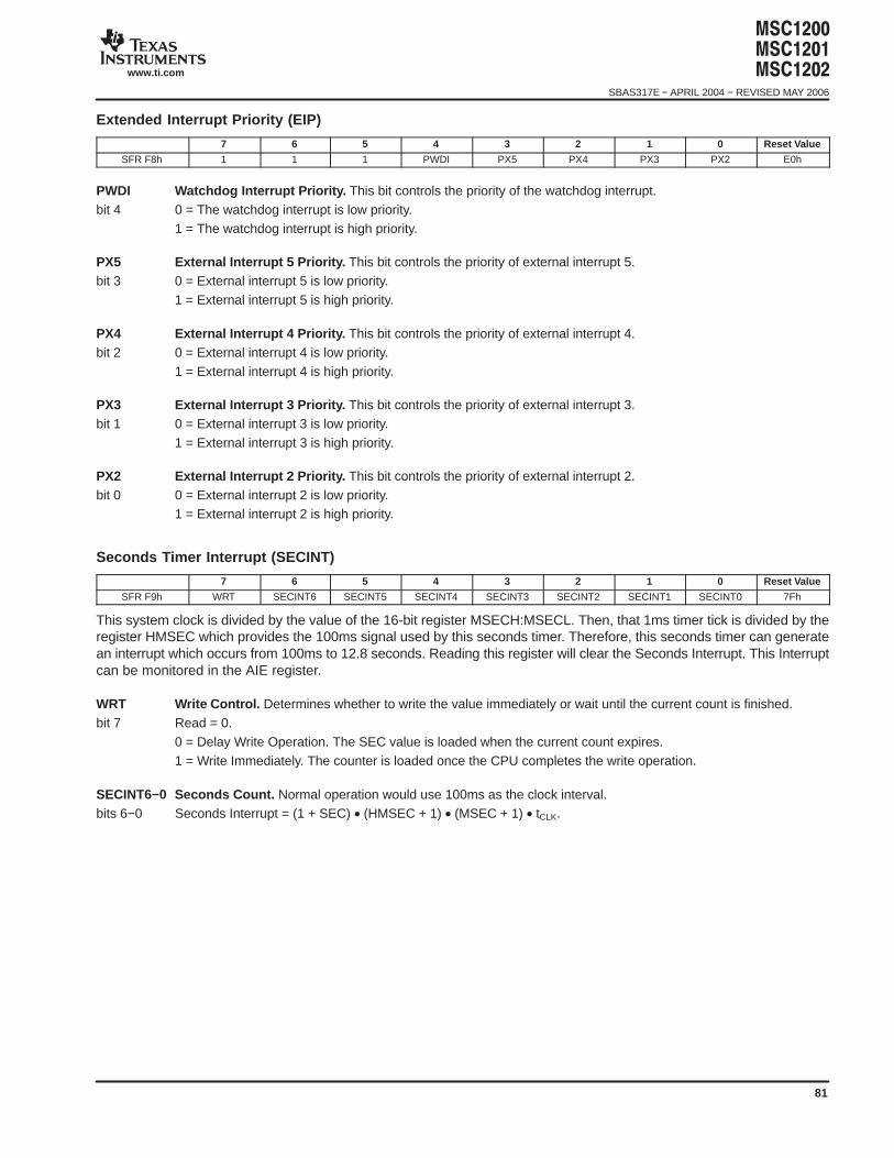
#$#$#$$
SBAS317E − APRIL 2004 − REVISED MAY 2006
www.ti.com
81
Extended Interrupt Priority (EIP)
7 6 5 4 3 2 1 0 Reset Value
SFR F8h 1 1 1 PWDI PX5 PX4 PX3 PX2 E0h
PWDI Watchdog Interrupt Priority. This bit controls the priority of the watchdog interrupt.bit 4 0 = The watchdog interrupt is low priority.
1 = The watchdog interrupt is high priority.
PX5 External Interrupt 5 Priority. This bit controls the priority of external interrupt 5.bit 3 0 = External interrupt 5 is low priority.
1 = External interrupt 5 is high priority.
PX4 External Interrupt 4 Priority. This bit controls the priority of external interrupt 4.bit 2 0 = External interrupt 4 is low priority.
1 = External interrupt 4 is high priority.
PX3 External Interrupt 3 Priority. This bit controls the priority of external interrupt 3.bit 1 0 = External interrupt 3 is low priority.
1 = External interrupt 3 is high priority.
PX2 External Interrupt 2 Priority. This bit controls the priority of external interrupt 2.bit 0 0 = External interrupt 2 is low priority.
1 = External interrupt 2 is high priority.
Seconds Timer Interrupt (SECINT)
7 6 5 4 3 2 1 0 Reset Value
SFR F9h WRT SECINT6 SECINT5 SECINT4 SECINT3 SECINT2 SECINT1 SECINT0 7Fh
This system clock is divided by the value of the 16-bit register MSECH:MSECL. Then, that 1ms timer tick is divided by theregister HMSEC which provides the 100ms signal used by this seconds timer. Therefore, this seconds timer can generatean interrupt which occurs from 100ms to 12.8 seconds. Reading this register will clear the Seconds Interrupt. This Interruptcan be monitored in the AIE register.
WRT Write Control. Determines whether to write the value immediately or wait until the current count is finished.bit 7 Read = 0.
0 = Delay Write Operation. The SEC value is loaded when the current count expires.1 = Write Immediately. The counter is loaded once the CPU completes the write operation.
SECINT6−0 Seconds Count. Normal operation would use 100ms as the clock interval.bits 6−0 Seconds Interrupt = (1 + SEC) • (HMSEC + 1) • (MSEC + 1) • tCLK.
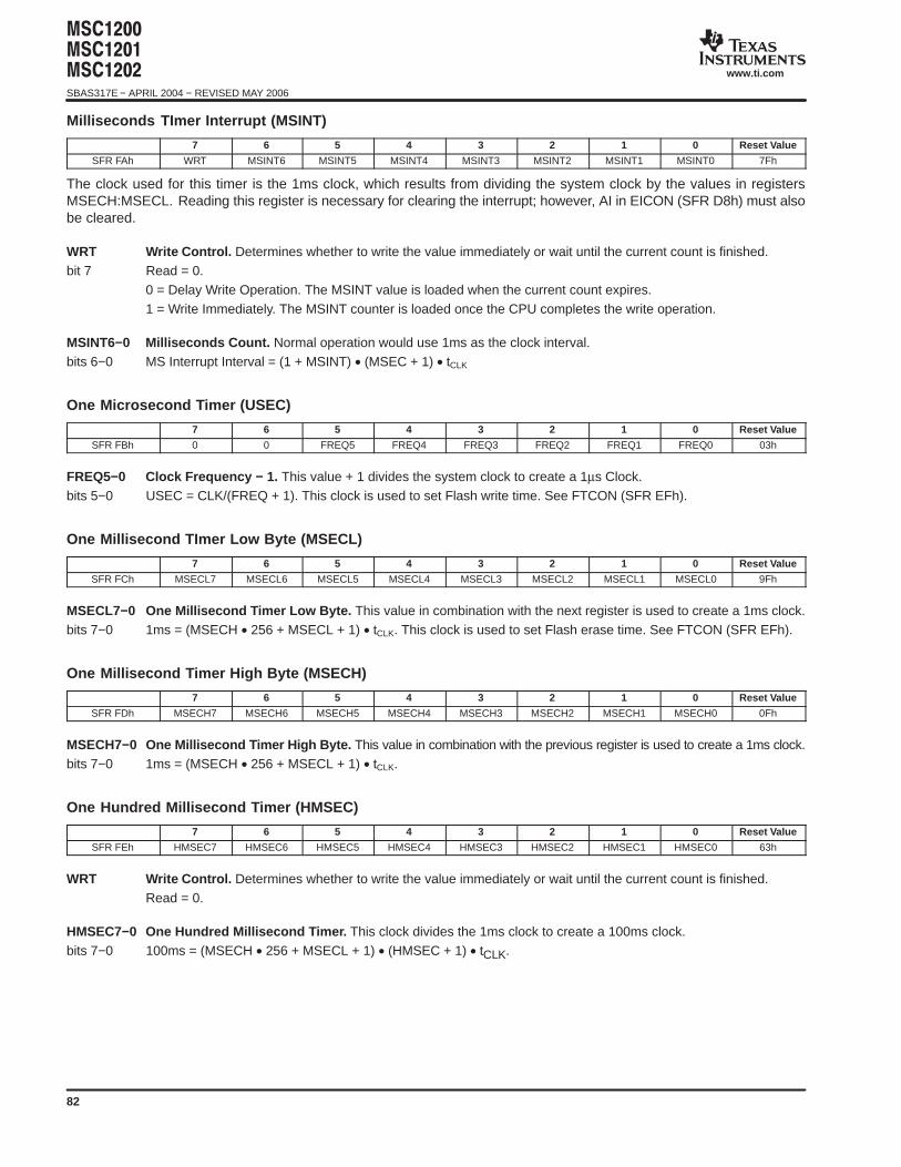
#$#$#$$SBAS317E − APRIL 2004 − REVISED MAY 2006
www.ti.com
82
Milliseconds TImer Interrupt (MSINT)
7 6 5 4 3 2 1 0 Reset Value
SFR FAh WRT MSINT6 MSINT5 MSINT4 MSINT3 MSINT2 MSINT1 MSINT0 7Fh
The clock used for this timer is the 1ms clock, which results from dividing the system clock by the values in registersMSECH:MSECL. Reading this register is necessary for clearing the interrupt; however, AI in EICON (SFR D8h) must alsobe cleared.
WRT Write Control. Determines whether to write the value immediately or wait until the current count is finished.bit 7 Read = 0.
0 = Delay Write Operation. The MSINT value is loaded when the current count expires.1 = Write Immediately. The MSINT counter is loaded once the CPU completes the write operation.
MSINT6−0 Milliseconds Count. Normal operation would use 1ms as the clock interval.bits 6−0 MS Interrupt Interval = (1 + MSINT) • (MSEC + 1) • tCLK
One Microsecond Timer (USEC)
7 6 5 4 3 2 1 0 Reset Value
SFR FBh 0 0 FREQ5 FREQ4 FREQ3 FREQ2 FREQ1 FREQ0 03h
FREQ5−0 Clock Frequency − 1. This value + 1 divides the system clock to create a 1µs Clock.bits 5−0 USEC = CLK/(FREQ + 1). This clock is used to set Flash write time. See FTCON (SFR EFh).
One Millisecond TImer Low Byte (MSECL)
7 6 5 4 3 2 1 0 Reset Value
SFR FCh MSECL7 MSECL6 MSECL5 MSECL4 MSECL3 MSECL2 MSECL1 MSECL0 9Fh
MSECL7−0 One Millisecond Timer Low Byte. This value in combination with the next register is used to create a 1ms clock.bits 7−0 1ms = (MSECH • 256 + MSECL + 1) • tCLK. This clock is used to set Flash erase time. See FTCON (SFR EFh).
One Millisecond Timer High Byte (MSECH)
7 6 5 4 3 2 1 0 Reset Value
SFR FDh MSECH7 MSECH6 MSECH5 MSECH4 MSECH3 MSECH2 MSECH1 MSECH0 0Fh
MSECH7−0 One Millisecond T imer High Byte. This value in combination with the previous register is used to create a 1ms clock.bits 7−0 1ms = (MSECH • 256 + MSECL + 1) • tCLK.
One Hundred Millisecond Timer (HMSEC)
7 6 5 4 3 2 1 0 Reset Value
SFR FEh HMSEC7 HMSEC6 HMSEC5 HMSEC4 HMSEC3 HMSEC2 HMSEC1 HMSEC0 63h
WRT Write Control. Determines whether to write the value immediately or wait until the current count is finished.Read = 0.
HMSEC7−0 One Hundred Millisecond Timer. This clock divides the 1ms clock to create a 100ms clock.bits 7−0 100ms = (MSECH • 256 + MSECL + 1) • (HMSEC + 1) • tCLK.
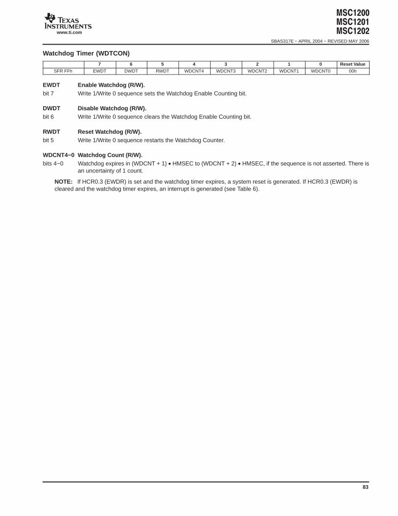
#$#$#$$
SBAS317E − APRIL 2004 − REVISED MAY 2006
www.ti.com
83
Watchdog Timer (WDTCON)
7 6 5 4 3 2 1 0 Reset Value
SFR FFh EWDT DWDT RWDT WDCNT4 WDCNT3 WDCNT2 WDCNT1 WDCNT0 00h
EWDT Enable Watchdog (R/W).bit 7 Write 1/Write 0 sequence sets the Watchdog Enable Counting bit.
DWDT Disable Watchdog (R/W).bit 6 Write 1/Write 0 sequence clears the Watchdog Enable Counting bit.
RWDT Reset Watchdog (R/W).bit 5 Write 1/Write 0 sequence restarts the Watchdog Counter.
WDCNT4−0 Watchdog Count (R/W).bits 4−0 Watchdog expires in (WDCNT + 1) • HMSEC to (WDCNT + 2) • HMSEC, if the sequence is not asserted. There is
an uncertainty of 1 count.
NOTE: If HCR0.3 (EWDR) is set and the watchdog timer expires, a system reset is generated. If HCR0.3 (EWDR) iscleared and the watchdog timer expires, an interrupt is generated (see Table 6).
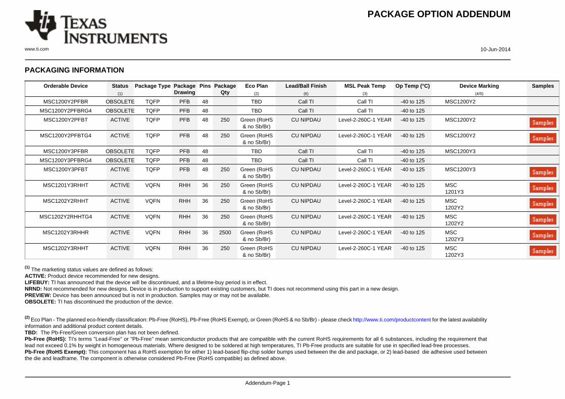
PACKAGE OPTION ADDENDUM
www.ti.com 10-Jun-2014
Addendum-Page 1
PACKAGING INFORMATION
Orderable Device Status(1)
Package Type PackageDrawing
Pins PackageQty
Eco Plan(2)
Lead/Ball Finish(6)
MSL Peak Temp(3)
Op Temp (°C) Device Marking(4/5)
Samples
MSC1200Y2PFBR OBSOLETE TQFP PFB 48 TBD Call TI Call TI -40 to 125 MSC1200Y2
MSC1200Y2PFBRG4 OBSOLETE TQFP PFB 48 TBD Call TI Call TI -40 to 125
MSC1200Y2PFBT ACTIVE TQFP PFB 48 250 Green (RoHS& no Sb/Br)
CU NIPDAU Level-2-260C-1 YEAR -40 to 125 MSC1200Y2
MSC1200Y2PFBTG4 ACTIVE TQFP PFB 48 250 Green (RoHS& no Sb/Br)
CU NIPDAU Level-2-260C-1 YEAR -40 to 125 MSC1200Y2
MSC1200Y3PFBR OBSOLETE TQFP PFB 48 TBD Call TI Call TI -40 to 125 MSC1200Y3
MSC1200Y3PFBRG4 OBSOLETE TQFP PFB 48 TBD Call TI Call TI -40 to 125
MSC1200Y3PFBT ACTIVE TQFP PFB 48 250 Green (RoHS& no Sb/Br)
CU NIPDAU Level-2-260C-1 YEAR -40 to 125 MSC1200Y3
MSC1201Y3RHHT ACTIVE VQFN RHH 36 250 Green (RoHS& no Sb/Br)
CU NIPDAU Level-2-260C-1 YEAR -40 to 125 MSC1201Y3
MSC1202Y2RHHT ACTIVE VQFN RHH 36 250 Green (RoHS& no Sb/Br)
CU NIPDAU Level-2-260C-1 YEAR -40 to 125 MSC1202Y2
MSC1202Y2RHHTG4 ACTIVE VQFN RHH 36 250 Green (RoHS& no Sb/Br)
CU NIPDAU Level-2-260C-1 YEAR -40 to 125 MSC1202Y2
MSC1202Y3RHHR ACTIVE VQFN RHH 36 2500 Green (RoHS& no Sb/Br)
CU NIPDAU Level-2-260C-1 YEAR -40 to 125 MSC1202Y3
MSC1202Y3RHHT ACTIVE VQFN RHH 36 250 Green (RoHS& no Sb/Br)
CU NIPDAU Level-2-260C-1 YEAR -40 to 125 MSC1202Y3
(1) The marketing status values are defined as follows:ACTIVE: Product device recommended for new designs.LIFEBUY: TI has announced that the device will be discontinued, and a lifetime-buy period is in effect.NRND: Not recommended for new designs. Device is in production to support existing customers, but TI does not recommend using this part in a new design.PREVIEW: Device has been announced but is not in production. Samples may or may not be available.OBSOLETE: TI has discontinued the production of the device.
(2) Eco Plan - The planned eco-friendly classification: Pb-Free (RoHS), Pb-Free (RoHS Exempt), or Green (RoHS & no Sb/Br) - please check http://www.ti.com/productcontent for the latest availabilityinformation and additional product content details.TBD: The Pb-Free/Green conversion plan has not been defined.Pb-Free (RoHS): TI's terms "Lead-Free" or "Pb-Free" mean semiconductor products that are compatible with the current RoHS requirements for all 6 substances, including the requirement thatlead not exceed 0.1% by weight in homogeneous materials. Where designed to be soldered at high temperatures, TI Pb-Free products are suitable for use in specified lead-free processes.Pb-Free (RoHS Exempt): This component has a RoHS exemption for either 1) lead-based flip-chip solder bumps used between the die and package, or 2) lead-based die adhesive used betweenthe die and leadframe. The component is otherwise considered Pb-Free (RoHS compatible) as defined above.
PACKAGE OPTION ADDENDUM
www.ti.com 10-Jun-2014
Addendum-Page 2
Green (RoHS & no Sb/Br): TI defines "Green" to mean Pb-Free (RoHS compatible), and free of Bromine (Br) and Antimony (Sb) based flame retardants (Br or Sb do not exceed 0.1% by weightin homogeneous material)
(3) MSL, Peak Temp. - The Moisture Sensitivity Level rating according to the JEDEC industry standard classifications, and peak solder temperature.
(4) There may be additional marking, which relates to the logo, the lot trace code information, or the environmental category on the device.
(5) Multiple Device Markings will be inside parentheses. Only one Device Marking contained in parentheses and separated by a "~" will appear on a device. If a line is indented then it is a continuationof the previous line and the two combined represent the entire Device Marking for that device.
(6) Lead/Ball Finish - Orderable Devices may have multiple material finish options. Finish options are separated by a vertical ruled line. Lead/Ball Finish values may wrap to two lines if the finishvalue exceeds the maximum column width.
Important Information and Disclaimer:The information provided on this page represents TI's knowledge and belief as of the date that it is provided. TI bases its knowledge and belief on informationprovided by third parties, and makes no representation or warranty as to the accuracy of such information. Efforts are underway to better integrate information from third parties. TI has taken andcontinues to take reasonable steps to provide representative and accurate information but may not have conducted destructive testing or chemical analysis on incoming materials and chemicals.TI and TI suppliers consider certain information to be proprietary, and thus CAS numbers and other limited information may not be available for release.
In no event shall TI's liability arising out of such information exceed the total purchase price of the TI part(s) at issue in this document sold by TI to Customer on an annual basis.
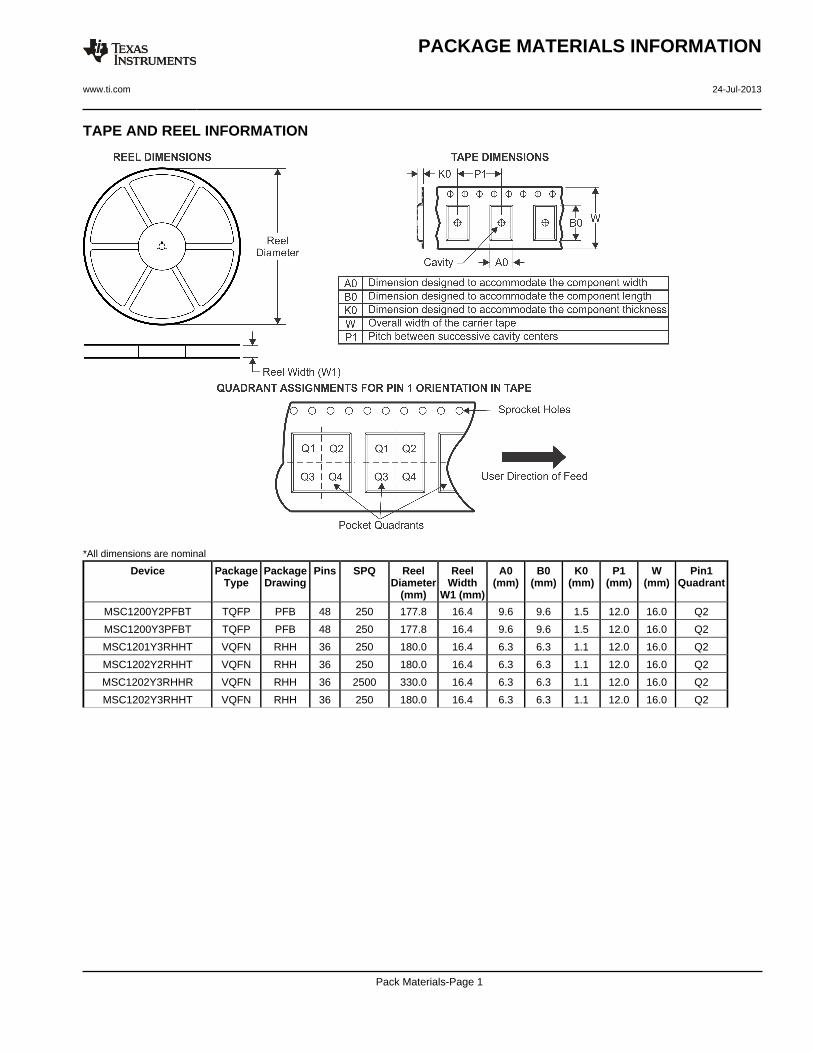
TAPE AND REEL INFORMATION
*All dimensions are nominal
Device PackageType
PackageDrawing
Pins SPQ ReelDiameter
(mm)
ReelWidth
W1 (mm)
A0(mm)
B0(mm)
K0(mm)
P1(mm)
W(mm)
Pin1Quadrant
MSC1200Y2PFBT TQFP PFB 48 250 177.8 16.4 9.6 9.6 1.5 12.0 16.0 Q2
MSC1200Y3PFBT TQFP PFB 48 250 177.8 16.4 9.6 9.6 1.5 12.0 16.0 Q2
MSC1201Y3RHHT VQFN RHH 36 250 180.0 16.4 6.3 6.3 1.1 12.0 16.0 Q2
MSC1202Y2RHHT VQFN RHH 36 250 180.0 16.4 6.3 6.3 1.1 12.0 16.0 Q2
MSC1202Y3RHHR VQFN RHH 36 2500 330.0 16.4 6.3 6.3 1.1 12.0 16.0 Q2
MSC1202Y3RHHT VQFN RHH 36 250 180.0 16.4 6.3 6.3 1.1 12.0 16.0 Q2
PACKAGE MATERIALS INFORMATION
www.ti.com 24-Jul-2013
Pack Materials-Page 1
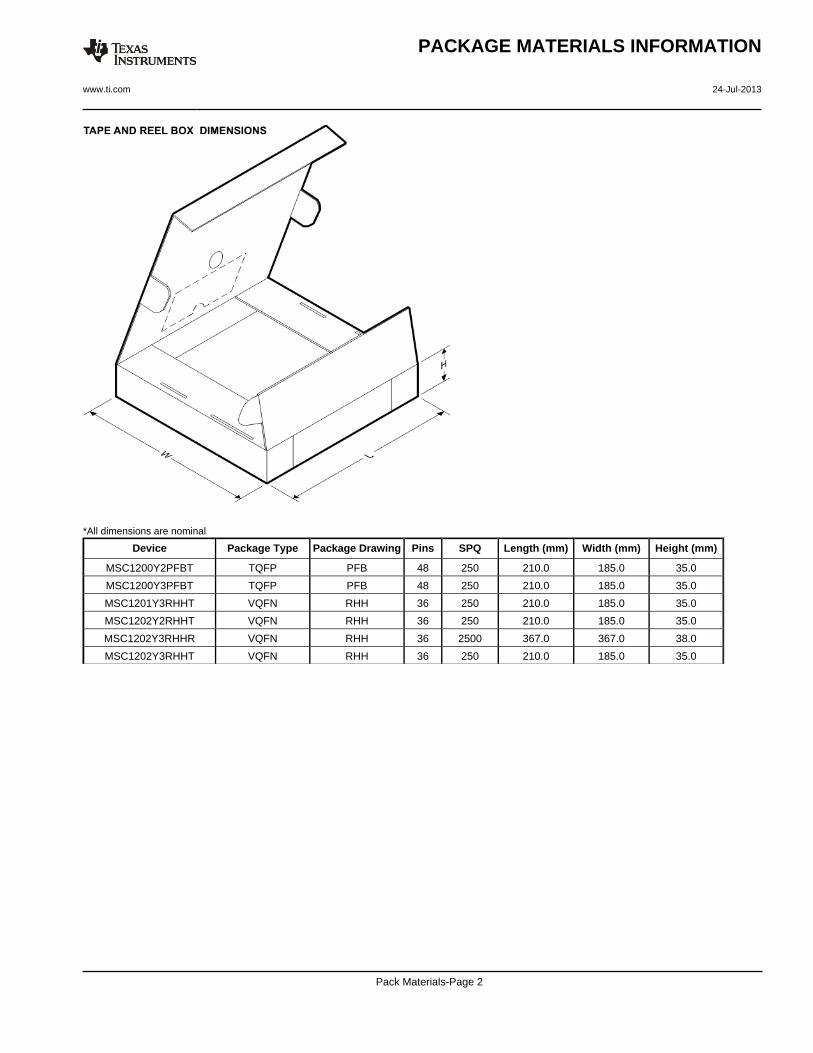
*All dimensions are nominal
Device Package Type Package Drawing Pins SPQ Length (mm) Width (mm) Height (mm)
MSC1200Y2PFBT TQFP PFB 48 250 210.0 185.0 35.0
MSC1200Y3PFBT TQFP PFB 48 250 210.0 185.0 35.0
MSC1201Y3RHHT VQFN RHH 36 250 210.0 185.0 35.0
MSC1202Y2RHHT VQFN RHH 36 250 210.0 185.0 35.0
MSC1202Y3RHHR VQFN RHH 36 2500 367.0 367.0 38.0
MSC1202Y3RHHT VQFN RHH 36 250 210.0 185.0 35.0
PACKAGE MATERIALS INFORMATION
www.ti.com 24-Jul-2013
Pack Materials-Page 2
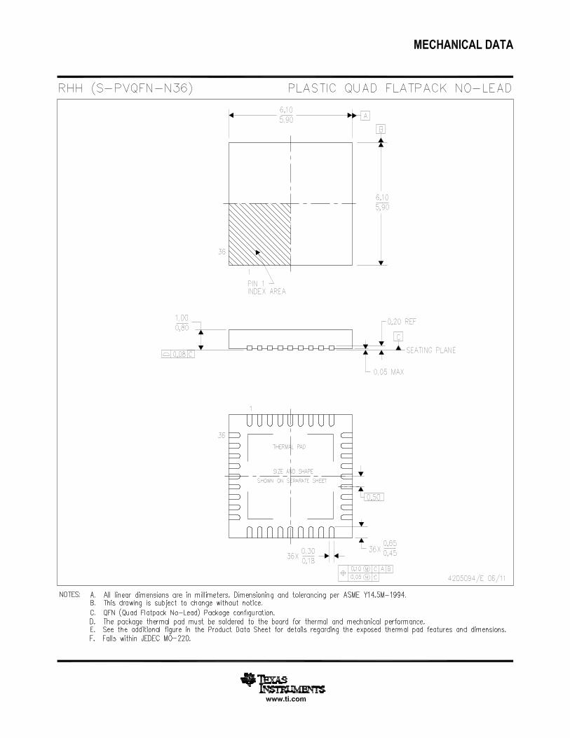
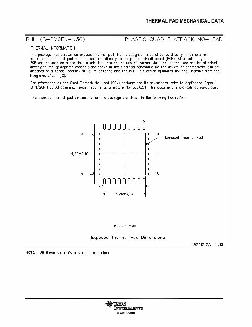
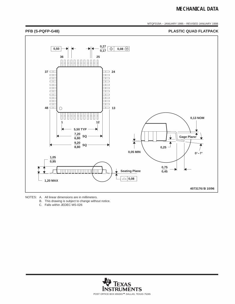
MECHANICAL DATA
MTQF019A – JANUARY 1995 – REVISED JANUARY 1998
POST OFFICE BOX 655303 • DALLAS, TEXAS 75265
PFB (S-PQFP-G48) PLASTIC QUAD FLATPACK
4073176/B 10/96
Gage Plane
0,13 NOM
0,25
0,450,75
Seating Plane
0,05 MIN
0,170,27
24
25
13
12
SQ
36
37
7,206,80
48
1
5,50 TYP
SQ8,809,20
1,050,95
1,20 MAX0,08
0,50 M0,08
0°–7°
NOTES: A. All linear dimensions are in millimeters.B. This drawing is subject to change without notice.C. Falls within JEDEC MS-026
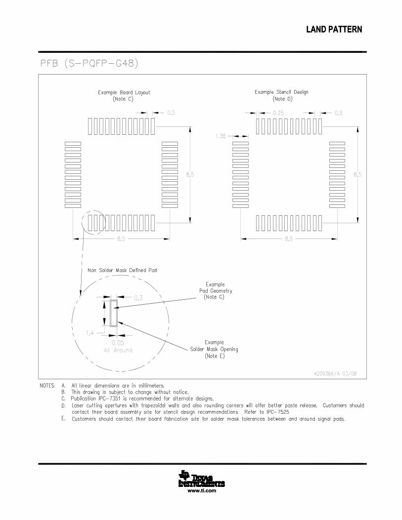

IMPORTANT NOTICETexas Instruments Incorporated and its subsidiaries (TI) reserve the right to make corrections, enhancements, improvements and otherchanges to its semiconductor products and services per JESD46, latest issue, and to discontinue any product or service per JESD48, latestissue. Buyers should obtain the latest relevant information before placing orders and should verify that such information is current andcomplete. All semiconductor products (also referred to herein as “components”) are sold subject to TI’s terms and conditions of salesupplied at the time of order acknowledgment.TI warrants performance of its components to the specifications applicable at the time of sale, in accordance with the warranty in TI’s termsand conditions of sale of semiconductor products. Testing and other quality control techniques are used to the extent TI deems necessaryto support this warranty. Except where mandated by applicable law, testing of all parameters of each component is not necessarilyperformed.TI assumes no liability for applications assistance or the design of Buyers’ products. Buyers are responsible for their products andapplications using TI components. To minimize the risks associated with Buyers’ products and applications, Buyers should provideadequate design and operating safeguards.TI does not warrant or represent that any license, either express or implied, is granted under any patent right, copyright, mask work right, orother intellectual property right relating to any combination, machine, or process in which TI components or services are used. Informationpublished by TI regarding third-party products or services does not constitute a license to use such products or services or a warranty orendorsement thereof. Use of such information may require a license from a third party under the patents or other intellectual property of thethird party, or a license from TI under the patents or other intellectual property of TI.Reproduction of significant portions of TI information in TI data books or data sheets is permissible only if reproduction is without alterationand is accompanied by all associated warranties, conditions, limitations, and notices. TI is not responsible or liable for such altereddocumentation. Information of third parties may be subject to additional restrictions.Resale of TI components or services with statements different from or beyond the parameters stated by TI for that component or servicevoids all express and any implied warranties for the associated TI component or service and is an unfair and deceptive business practice.TI is not responsible or liable for any such statements.Buyer acknowledges and agrees that it is solely responsible for compliance with all legal, regulatory and safety-related requirementsconcerning its products, and any use of TI components in its applications, notwithstanding any applications-related information or supportthat may be provided by TI. Buyer represents and agrees that it has all the necessary expertise to create and implement safeguards whichanticipate dangerous consequences of failures, monitor failures and their consequences, lessen the likelihood of failures that might causeharm and take appropriate remedial actions. Buyer will fully indemnify TI and its representatives against any damages arising out of the useof any TI components in safety-critical applications.In some cases, TI components may be promoted specifically to facilitate safety-related applications. With such components, TI’s goal is tohelp enable customers to design and create their own end-product solutions that meet applicable functional safety standards andrequirements. Nonetheless, such components are subject to these terms.No TI components are authorized for use in FDA Class III (or similar life-critical medical equipment) unless authorized officers of the partieshave executed a special agreement specifically governing such use.Only those TI components which TI has specifically designated as military grade or “enhanced plastic” are designed and intended for use inmilitary/aerospace applications or environments. Buyer acknowledges and agrees that any military or aerospace use of TI componentswhich have not been so designated is solely at the Buyer's risk, and that Buyer is solely responsible for compliance with all legal andregulatory requirements in connection with such use.TI has specifically designated certain components as meeting ISO/TS16949 requirements, mainly for automotive use. In any case of use ofnon-designated products, TI will not be responsible for any failure to meet ISO/TS16949.Products ApplicationsAudio www.ti.com/audio Automotive and Transportation www.ti.com/automotiveAmplifiers amplifier.ti.com Communications and Telecom www.ti.com/communicationsData Converters dataconverter.ti.com Computers and Peripherals www.ti.com/computersDLP® Products www.dlp.com Consumer Electronics www.ti.com/consumer-appsDSP dsp.ti.com Energy and Lighting www.ti.com/energyClocks and Timers www.ti.com/clocks Industrial www.ti.com/industrialInterface interface.ti.com Medical www.ti.com/medicalLogic logic.ti.com Security www.ti.com/securityPower Mgmt power.ti.com Space, Avionics and Defense www.ti.com/space-avionics-defenseMicrocontrollers microcontroller.ti.com Video and Imaging www.ti.com/videoRFID www.ti-rfid.comOMAP Applications Processors www.ti.com/omap TI E2E Community e2e.ti.comWireless Connectivity www.ti.com/wirelessconnectivity
Mailing Address: Texas Instruments, Post Office Box 655303, Dallas, Texas 75265Copyright © 2014, Texas Instruments Incorporated