principles of power measurement - boonton
TRANSCRIPT

Principles of Power Measurement
A Primer on RF & Microwave Power Measurement


Principles of Power Measurement
A Primer on RF & Microwave Power Measurement
As we constantly strive to improve our products, the information in this document gives only a general indication of the product capacity, performance and suitability, none of which shall form part of any contract. We reserve the right to make design changes without notice. This material has been complied from a number of sources and Wireless Telecom Group accepts no responsibility for errors or omissions.
Parent company Wireless Telecom Group © Wireless Telecom Group, 2011. All trademarks are acknowledged .
www.WirelessTelecomGroup.com


iii
About UsWireless Telecom Group is a global designer and manufacturer of radio frequency (“RF”) and micro-
wave-based products for wireless and advanced communications industries. We market our prod-
ucts and services worldwide under the Boonton Electronics (“Boonton”), Microlab/FXR (“Microlab”)
and Noisecom brands. Our Brands and products have maintained a reputation for their accuracy and
performance as they support our customers’ technological advancements within communications.
We offer our customers a complementary suite of high performance instruments and components
meeting a variety of standards including peak power meters, signal analyzers, noise sources, power
splitters, combiners, diplexers, noise modules and precision noise generators. We serve commercial
and government markets within the satellite, cable, radar, avionics, medical, and computing applica-
tions. We are headquartered in Parsippany, New Jersey, in the New York City metropolitan area and we
maintain a global network of Sales offices dedicated to providing excellent product support.
Wireless Telecom Group, Inc. continuously targets opportunities that allow us to capitalize on our
synergies and our talents. Our technological capabilities along with our customer service strategies
remain essential competencies for our success.

iv
Section 1 RF and Microwave Power Measurement Fundamentals 1
Chapter 1: Power Measurement Basics 3
1.1 What is Power? 3
1.2 Why Measure Power? 5
1.3 Power Measurement History 7
Chapter 2: Power Measurement Technologies 11
2.1 Thermal RF Power Sensors 11
2.2 Detector (diode) RF Power Sensors 14
2.3 Receiver-based Amplitude Measurement 18
2.4 Monolithic Amplitude Measurement 19
2.5 Direct RF Sampling Amplitude Measurement 19
2.6 What is an RF Power Meter? 20
Chapter 3: CW, Average and Peak Power 23
3.1 CW Power Meter Limitations 23
3.2 The “Peak Power” Solution 24
3.3 It’s all about Bandwidth 25
3.4 Understanding the Importance of Dynamic Range 27
Section 2 Making Power Measurements 31
Chapter 4: Equipment Selection 33
4.1 Choosing the Right Power Meter 33
4.2 Choosing an RF Power Sensor 35
4.3 Selecting a Measurement Mode 37
4.4 Power Meters versus Spectrum Analyzers 40
4.5 Oscilloscopes and Detectors 48
Chapter 5: Calibration Issues 52
5.1 Factory Open-loop Calibration 52
5.2 Single, Double, and Multipoint Linearity Calibration 53
5.3 Field Linearity Calibration Methods 56
5.4 Frequency Response Correction 59
Principles of Power Measurement
Table of Contents
A Primer on RF & Microwave Power Measurement

vTable of Contents
Chapter 6: RF Power Analysis 62
6.1 Continuous Measurements 63
6.2 Triggered and Pulse Analysis 64
6.3 Statistical Power Analysis 68
Chapter 7: Power Measurement Applications 75
7.1 Low Duty-Cycle Pulse Measurements 75
7.2 Statistical Analysis of Modern Communication Signals 80
7.3 Using Power Meters for EMC Testing 87
Chapter 8: Performance Tips 91
8.1 Reducing Measurement Noise 91
8.2 Optimizing ATE Performance 94
8.3 Communication Amplifier Testing 104
Chapter 9: Measurement Accuracy 110
9.1 Introduction to Uncertainty 110
9.2 Power Measurement Uncertainty Contributions 112
9.3 Sample Uncertainty Calculations 116
Section 3 Power Measurement Reference 125
Chapter 10: Reference Tables 126
10.1 Amplitude Measurement Conversions 126
10.2 Return Loss / Reflection Coefficient / VSWR Conversions 127
10.3 Wireless and Radar/Microwave Bands 129
10.4 Sensor Cable Length Effects 129
Chapter 11: Boonton Solutions 131
11.1 4240 Series RF Power Meter 131
11.2 4530 Series RF Power Meter 132
11.3 4540 Series RF Power Meter 133
11.4 4500B RF Peak Power Analyzer 134
11.5 Boonton CW and Peak RF Power Sensors 135
11.6 Most Popular Peak Sensors 138

1
Section 1
RF & Microwave Power Measurement Fundamentals
RF Power Measurement is a broad topic that has been of importance to designers and operators since the earliest days of wire line and wireless communication and infor-mation transmission. With today’s complex modulation schemes, increased popular-ity of wireless transmission and pulsed communication modes, the need to accurately and efficiently measure RF power has become crucial to obtaining optimum perfor-mance from communication systems and components.

2Section 1: RF & Microwave Power Measurement Fundamentals
What is Power? A discussion of the physical definition of power, and the electrical con-cepts of volts, amps, and watts. This leads to how the measurement of AC and RF power is complicated by complex impedance and phase shift.
Why do we want to measure Power? There are many reasons to measure RF power, span-ning a wide range of industries and technologies. This subsection discusses the common uses of power measurement instruments, and the rationale.
A brief history of RF power measurements. Power measurement has evolved consider-ably since the earliest days of wireless. Some of this history can be traced to well-known radio pioneers, and much of the innovation took place among companies still involved in the measurement industry. A considerable amount of history took place in the northern New Jersey region that is still home to Boonton Electronics.
Power Measurement Technologies. A discussion of the key methods in use today for measuring RF power, including Thermal, Diode, Receiver-based, Direct RF Sampling, and Monolithic (IC) solutions.
CW versus Peak Power. Power measurement has come a long way since early methods, which only produced meaningful measurements for unmodulated signals. This section focuses on the limitations of various types of power meters when measuring modulated signals, and how modern solutions have improved the situation.
Bandwidth and Dynamic Range Issues. Not every signal aligns neatly with the capabili-ties of power measurement instruments. By understanding the bandwidth and dynamic range characteristics of your signal, it becomes easier to select the best measurement tech-nology.

3
Chapter 1: Power Measurement Basics
1.1 What is Power?In physics terms, power is the transfer rate of energy per unit time. Just as energy has many different forms (kinetic, potential, heat, electrical, chemical), so does power. One mechanical definition of energy is force multiplied by distance – the force moving an object multiplied by the distance it is moved.
Energy = Force x Distance
To get the power, or transfer rate of that energy, we divide that energy by the length of time to perform the move. Since distance per unit time is velocity, mechanical power is often computed as force times velocity.
Power = Force x Distance / Time = Force x Velocity
In electrical terms, force equates to voltage, also known as Electromotive Force (EMF). This describes how much “pressure” the electrons are under to move. The velocity is analogous to electrical current, which is the charge (number of electrons) per unit time.
Power(electrical) = EMF x Current
EMF is typically measured in volts, and current is typically measured in amperes, or amps. One ampere is one coulomb (a unit of charge, equal to 6.2 x 10¹⁸ electrons) per second. Multiplying current and voltage together yields the power in watts.
Watts = Volts x Amps
In the case of steady voltage or steady current flow, computing the average power is simple – just multiply average volts by average amps. However, if both values fluctuate, as will be the case with alternating current, or AC, the average power can only be computed by performing a mathematical average of the instantaneous power over one or more full sig-nal periods.
Limiting our discussion only to sinusoidal, AC waveforms, we can see that the power will fluctuate in synchronization with the voltage and current. For resistive loads, the current and voltage will be in-phase. That is both will be positive at the same time, and both nega-tive. Analyzing graphically, one can see that either case produces positive power, since multiplying two negative numbers yields a positive result. See Fig. 1.1.1

4Chapter 1: Power Measurement Basics
If there is a phase shift between current and voltage, there will be times that the voltage and current are of opposite polarities, resulting in a negative power flow. This has the ef-fect of reducing the average power, even though the magnitude of the voltage and current has not changed.
For this reason, it is not generally sufficient to simply measure the voltage or current to characterize a signal’s power. A direct power measurement is best, in which the signal is applied to a precision termination (load), which keeps the voltage and current very close to in-phase. If this is done properly, a voltage measurement across the load can be performed to yield a meaningful power value, or the dissipated power can be computed directly by measuring the heating effect of the signal upon the load. This is discussed in great detail in the next section.
50 ohm Complex Load: 45 deg phase shift
-1.50
-1.25
-1.00
-0.75
-0.50
-0.25
0.00
0.25
0.50
0.75
1.00
1.25
1.50
0 360 720 1080 1440
Phase (degrees)
Volt
s
-0.06
-0.04
-0.02
0.00
0.02
0.04
0.06
Am
ps, W
atts
Voltage
Current
InstantaneousPower
AveragePower
50 ohm Resistive Load: 0 deg phase shift
-1.50
-1.25
-1.00
-0.75
-0.50
-0.25
0.00
0.25
0.50
0.75
1.00
1.25
1.50
0 360 720 1080 1440
Phase (degrees)
Vol
ts
-0.06
-0.04
-0.02
0.00
0.02
0.04
0.06
Am
ps, W
atts
Voltage
Current
InstantaneousPower
AveragePower
Figure 1.1.1 instantaneous and average power when voltage and current are in-phase with a resistive load (Top)
and when voltage and current are phase shifted due to complex load impedence (Bottom)

5
1.2 Why Measure Power?The first question is why measure power at all, rather than voltage? While it is true that very accurate and traceable voltage measurements can be performed at DC, this becomes more difficult with AC. At audio and low RF frequencies (below about 10 MHz), it can be practical to individually measure the current and voltage of a signal. As frequency increas-es, this becomes more difficult, and a power measurement is a simpler and more accurate method of measuring a signal’s amplitude.
As RF signals approach microwave frequencies, the propagation wavelength in conductors becomes much smaller, and signal reflections, standing waves, and impedance mismatch can all become very significant error sources. A properly designed power detector can minimize these effects and allow accurate, repeatable amplitude measurements. For these reasons, POWER has been adopted as the primary amplitude measurement quantity of any RF or microwave signal.
There are many reasons it may be necessary to measure RF power. The most common needs are for proof-of-design, regulatory, safety, system efficiency, and component protec-tion purposes, but there are thousands of unique applications for which RF power measure-ment is required or helpful.
In the communication and wireless industries, there are usually a number of regulatory specifications that must be met by any transmitting device, and maximum transmitted power is almost always near the top of the list. The FCC and other regulatory agencies re-sponsible for wireless transmissions place strict limits on how much power may be radiated in specific bands to ensure that devices do not cause unacceptable interference to others. Although the real need is usually to limit the actual radiated energy, the more common and practical regulatory requirement is to specify the maximum power which may be delivered to the transmitting antenna.
Transmission interference

6Chapter 1: Power Measurement Basics
In addition to the regulatory issues, transmitter power needs to be limited in many communication systems to allow optimum use of wireless spectral and geographi-cal space. If two transmitting devices are operating in the same frequency band and physical proximity, receivers can have a more difficult time discriminating the sig-nals if one signal is much too large relative to the other. Even in commercial broad-cast, the transmitting power of each broadcast site is licensed and must be constantly monitored to ensure that operators do not interfere with other stations occupying the same or nearby frequencies in neighboring cities.
Controlling transmission power is particularly necessary in modern cellular networks, where operators constantly strive to maximize system capacity and throughput. Many modern wireless protocols use some form of multiplexing, in which multiple mobile transmitters (for example, cellular handsets) must simultaneously transmit data to a common base sta-tion. In these situations, it is necessary to carefully monitor and control the transmitted power of each device so that their signals arrive at the base station with approximately equal amplitudes. If one device on a channel has too much power, it will “step on” the transmission of other devices sharing that channel, and make it impossible for the base station to decode those signals.
Another power control issue in cellular systems is due to the close proximity of base sta-tions in congested areas. If a device is transmitting with too much power, it will not only interfere with signals in its own cell, but can possibly interfere with the transmissions of devices in neighboring cells. Mobile devices for these systems typically implement both open-loop and closed-loop, real-time power control of their transmitters. Without accurate power control of every single device within range of a base station, cellular network capac-ity can be severely degraded.
Too much power has other dangers as well. For higher power systems, too much RF power can present biological hazards to personnel and animals. Safety limits are often placed on transmitted power to protect users and bystanders from the dangers of high-power RF radiation. A good example of the potential dangers of RF energy is a common microwave oven, which can severely burn human flesh just as easily as it can heat a meal. Radio and RADAR transmitters operate at still higher power levels, and present their own special haz-ards. It is hypothesized that even low-power RF transmitting devices such as cell phones may have potential to cause lasting biological effects. In all of these cases, there will be times when the actual power present must be monitored to ensure compliance with safety standards or guidelines.

7
Measuring power is important for circuit designers as well. Any electronic device can be overloaded or damaged by too high a signal. Too much steady-state power can cause heating effects and destroy passive and active components alike. Too much instantaneous (“peak”) power can overstress semiconductor devices, or cause dielectric breakdown or arcing in passive components, connectors, and cables.
But even at power levels well below the damage threshold of the circuit components, ex-cessive power can cause overload of system, clipping, distortion, data loss or a number of other adverse effects. Similarly, insufficient power can cause a signal to fall below the noise floor of a transmission system, again resulting in signal degradation or loss.
1.3 Power Measurement HistorySince the late 1800s, when Nikola Tesla first demonstrated wireless transmission, there has been a need to measure the output of RF circuits. A major focus of Telsa’s work was wire-less transmission of electrical power, so he was often working in the megawatt range, and a relative indication of power was the discharge length of the “RF lightning” he produced. For obvious reasons, there was little incentive to attempt any sort of “contact” measure-ment!
Around 1888, an Austrian physicist named Ernst Lecher developed his “wires” technique as a method for measuring the frequency of an RF or microwave oscillator. The apparatus, of-ten known as Lecher Wires, consisted of two parallel rods or wires, held a constant distance apart, with a sliding short circuit between them. The wires formed an RF transmission line, and by moving the shorting bar, Lecher could create standing waves in the line, resulting in a series of the peaks and nulls. By measuring the physical distance between two peaks or two nulls, the signal’s wavelength in the transmission line, and thus its frequency could be calculated.
Initially, Lecher used a simple incandescent light bulb across the lines as power detector to locate the peaks and nulls. The apparent brightness of the bulb at the peaks also gave him a rough indication of the oscillator’s output amplitude. One of the problems with using a bulb, however, was that the low (and variable) impedance of its filament changed the line’s characteristics, and could affect the resonant frequency and output amplitude of the oscillator.
This was addressed by substituting a high-impedance, gas-discharge glow tube for the incandescent bulb. The glass tube was laid directly across the wires, and the field from a medium-voltage RF signal was adequate to excite a glow discharge in the gas tube. This didn’t change the tank impedance as much, while keeping it easy to visually determine the peak and null locations as the tube was slid up and down the wires. Later, a neon bulb was used, but the higher striking voltage of neon made the nulls difficult to locate precisely.

8Chapter 1: Power Measurement Basics
In 1933, H.V. Noble, a Westinghouse engineer, refined some of Tesla’s research, and was able to transmit several hundred watts at 100 MHz a distance of ten meters or so. This wireless RF power transmission was demonstrated at the Chicago World’s Fair at the West-inghouse exhibit. His frequencies were low enough that the transmitted and received signal voltages could be directly measured by conventional electronic devices of the day – vacuum tube and cat’s whisker detectors. At higher frequencies, however, these simple methods did not work as well – the tubes and cat’s whiskers of the day simply lost rectifica-tion efficiency and repeatability.
Historical photo of Tesla lightning
Earnst Lecher’s apparatus for measuring RF amplitude

9
The Varian brothers used another indicator technique in the late 1930s during their de-velopment of the Klystron. They drilled a small hole in the side of the resonant cavity and put a fluorescent screen next to it. A glow would indicate that the device was oscillating, and the brightness gave a very rough power indication as adjustments were made. In fact some small transmitters manufactured into the 1960s had a small incandescent or neon lamp in the final tank circuit for tuning. The tank was tuned for maximum lamp brightness. These techniques all fall more under the category of RF indicators than actual measure-ment instruments.
The water-flow calorimeter, a common device for other uses, was adapted for higher power RF measurements to measure the heating effect of RF energy, and found its way into use anywhere you could install a “dummy load.” By monitoring flow of water and temperature rise as it cooled the load, it was simple to measure long-term average power dissipated by the load.
The thermocouple is one of the oldest ways of directly measuring low RF power levels. This is done by measuring its heating effect upon a load, and is still in common use today for the measurement of “true-RMS” power. Thermocouple RF ammeters have been in use since before 1930 but were restricted to the lower frequencies. It was not until the 1970s that thermocouples were developed that allowed their use as sensors in the VHF and Microwave range.
In later years, thermocouples and semiconductor diodes improved both in sensitivity and high-frequency ability. By the mid 1940s, the fragile, galena-based “cat-whisker” de-tectors were being replaced by stable, durable packaged diodes that could be calibrated against known standards, and used for more general-purpose RF power measurement.
Diode-based power measurement was further improved in the 50s and 60s, and Boonton Electronics made some notable contributions to the industry, initially in RF voltage mea-surement. The Model 91B was introduced in 1958 and could measure from below one mil-livolt to several volts. With a suitable termination, this yielded a calibrated dynamic range of about -50 dBm to +22 dBm over a frequency range of 200 kHz to 500 MHz.
RF voltmeters and power meters continued to evolve throughout the 70s with the applica-tion of digital and microprocessor technology, but these were all “average-only” instru-ments and few had any ability to quantify peak measurements. When a pulsed signal had to be characterized, the accepted technique was to use an oscilloscope and crystal detector to view the waveform in a qualitative fashion, and perform an average power measure-ment on the composite signal using either a CW power meter or a higher power measure-ment such as a calorimeter.
10Chapter 1: Power Measurement Basics
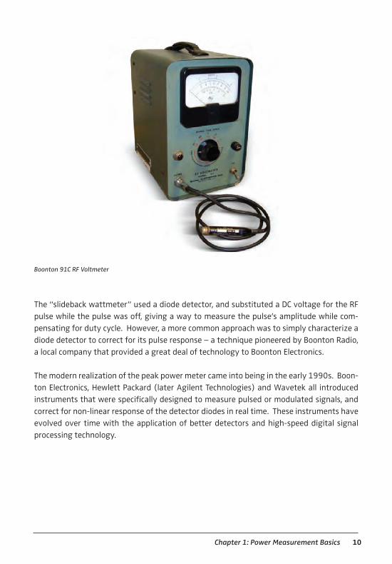
The “slideback wattmeter” used a diode detector, and substituted a DC voltage for the RF pulse while the pulse was off, giving a way to measure the pulse’s amplitude while com-pensating for duty cycle. However, a more common approach was to simply characterize a diode detector to correct for its pulse response – a technique pioneered by Boonton Radio, a local company that provided a great deal of technology to Boonton Electronics.
The modern realization of the peak power meter came into being in the early 1990s. Boon-ton Electronics, Hewlett Packard (later Agilent Technologies) and Wavetek all introduced instruments that were specifically designed to measure pulsed or modulated signals, and correct for non-linear response of the detector diodes in real time. These instruments have evolved over time with the application of better detectors and high-speed digital signal processing technology.
Boonton 91C RF Voltmeter

11
Chapter 2: Key Power Measurement Technologies There are a several different technologies available for the measurement of RF power. These generally fall into four categories:
Thermal The heating effect of RF power upon a sensing element is measured.Detector The RF signal is rectified or “detected” to yield a DC voltage proportional
to the signal’s amplitude.Receiver A “tuner” type circuit is used to receive the signal, then measure its
amplitude component.RF Sampling The RF signal is treated as a baseband AC signal, and is directly digitized. Both thermal and detector type measurements are typically “direct sensing,” in which the amplitude of the RF signal applied to a load element is measured by converting the RF to an easily-measured DC quantity. This RF-to-DC conversion is typically performed close to the signal source by connecting a small converter probe known as an RF power sensor to the device under test.
The receiver and RF sampling methods are usually indirect – the signal is brought into an instrument via a cable connection, processed through a multi-stage circuit to yield ampli-tude information, then scaled to power.
Following is a discussion of each of these technologies.
2.1 Thermal RF Power SensorsThermal sensors use the incoming RF energy to produce a temperature rise in a terminat-ing load. The temperature rise of the load is measured either directly or indirectly, and the corresponding input power is computed. The simplest is the early “light bulb” power detector used by Ernst Lecher in the late 1800s.
Thermistors
OR
Thermocouple
OR
Diode
Amplifier
Digitizer
Processing
DisplayRF Signal
Terminating
Power Detector
Power Meter Base Module
Cell Phone Radio
Base Station
Transmitter
RF Source
Proportional DC
Signal
Power Meter System
Direct Power Measurement Block Diagram

12Chapter 2: Key Power Measurement Technologies
Thermistor (Bolometer) sensors use a thermal element, known as a thermistor, as both the RF load and the temperature measurement device. The thermistor’s resistance changes with temperature, making it simple to measure its temperature by detecting in-circuit re-sistance.
The most common implementation places the thermistor element in one corner of a wheat-stone bridge, and uses a DC substitution technique, in which a controlled DC bias current is applied to the bridge to heat the thermistor until its resistance equals that of the other bridge resistors and the bridge is in balance. An auto-balancing circuit is used to amplify the bridge output and drive the entire bridge with this bias signal, heating the thermis-tor until balance is achieved. The net effect is that the thermistor will be operated at a constant temperature point where its resistance remains at the correct value to properly terminate the incoming RF – typically 50 or 100 ohms.
DC Bias Current
RF Power
Thermistor
R
-
+
RT
R
R
Thermistor Sensor Diagram
Bolometer
Sensor Reference
+Thermal Leak
DC
PowerTs Tr
Heat
Power
Bolometer Diagram

13
The total power dissipated by the thermistor is the sum of the incoming RF power and the power due to the DC bias. The power dissipated due to the RF heating can be computed by subtracting the thermistor’s reference “DC-only”power (measured and stored when no RF is applied) from its total (DC+RF) power. When the bridge is balanced, the thermistor’s dissipation due to the DC bias is easily computed as one-quarter of the total bridge power (bridge current multiplied by bridge voltage). The other three resistors in the bridge are designed to have a negligible temperature coefficient of resistance.
In practical implementations, there are two identical thermistor bridges, but only one is exposed to the RF. The second bridge is used to compensate for ambient temperature changes.
An RF signal is applied to the terminated load of a thermocouple sensor and the rise in temperature is measured. The rise in temperature is due to the Thermocouple Principle. A thermocouple is formed by a metallurgical junction between two dis-similar metals which produces a small voltage in response to a temperature gradi-ent across each metal segment – typically just a few tens of microvolts per degree C. In a practical thermocouple power sensor, a number of thermocouples may be electrically connected in series to form a thermopile. This increases the output voltage so it can be more easily amplified and measured by the meter. The thermopile often forms the RF load as well, and is connected in such a way that the RF energy flows through and heats only one end (the “hot junction”) of each thermocouple. This is done by capacitively coupling the RF while maintaining DC coupling for the output signal.
Hot
JunctionCold
JunctionVh
+
-
Iron Wire
Copper Wire
Weld Area
Iron Wire
Copper Wire
+
-
Hot
Junction
The voltage between wires is
produced by increasing the
temperature at the welded
junction
Diagram illustrating Thermocouple Principle

14Chapter 2: Key Power Measurement Technologies
The output voltage of a thermocouple type power sensor is very linear with input power and has a relatively long time constant due to heat flow delays. This means that they will tend to produce a reading which is proportional to the average of the applied RF power. Because of this, thermocouple sensors are commonly used for measuring the average pow-er of a modulated signal. Their relatively low sensitivity, however, limits their usefulness when the RF power level is less than several microwatts.
2.2 Detector (Diode) RF Power SensorsDiode sensors use high-frequency semiconductor diodes to detect the RF voltage devel-oped across a terminating load resistor. The diodes directly perform an AC to DC conver-sion, and the DC voltage is measured by the power meter and scaled to produce a power readout. In the strictest sense these are not power detectors, but rather voltage detectors, so termination impedance variations can cause more error in the reading due to mismatch than would be seen using thermal sensors. Early devices were simple crystal detectors us-ing galena and a cat-whisker to form a crude diode junction.
In a diode type RF power sensor, one or more diodes perform a rectification (peak detec-tion) function at high levels and act as a nonlinear resistor at lower levels, conducting more current in the forward direction than reverse. This is shown in Figure 2.2.1. Usually a smoothing capacitor is connected to the output of the diode to convert the pulsating DC to a steady DC voltage. Often, two diodes are used so both the positive and negative carrier cycles are detected; this makes the sensor relatively insensitive to even harmonic distor-tion. A diode detector’s DC output voltage is proportional to power at low signal levels and
+
+
+
+
+
+
+
+
+
+
Output Voltage
Copper Wire
Copper Wire
Copper Wire
Copper Wire
Copper Wire
Copper Wire
Iron Wire
Iron Wire
Iron Wire
Iron Wire
Iron Wire
Thermopile
Diagram illustrating a Thermopile

15
proportional to the peak RF voltage at higher levels. To achieve high sensitivities, the load resistance driven by the diode’s output is typically several megohms.
Below about -20 dBm (30mV peak carrier voltage), the RF input is not high enough to cause the diodes to fully conduct in the forward direction. Instead, they behave as non-lin-ear resistors as shown in Figure 2.2.2 below, and produce a DC output that is closely propor-tional to the square of the applied RF voltage. This is referred to as the “square-law” region of the diode sensor. When operated in this region, the average DC output voltage will be proportional to average RF power, even if modulation is present. This means a diode sensor can be used to measure the average power of a modulated signal, provided the instanta-neous (peak) power remains within the square-law region of the diodes at all times.
Above about 0 dBm (300mV peak input voltage), the diodes go into forward conduction on each cycle of the carrier, and the peak RF voltage is held by the smoothing capacitors. In this region, the sensor is behaving as a peak detector (also called an envelope detec-tor), and the DC output voltage will be equal to the peak-to-peak RF input voltage minus two diode drops. This is known as the “peak detecting” region of the diode sensor. When operated in this region, the average DC output voltage will be proportional to the peak RF voltage.
While the dynamic range of diode detectors is very large, operation in these two regions is quite different and the sensor’s response is not linear across its entire dynamic range. The square-law and peak-detecting regions, as well as the “transition region” between them (typically from about –20 dBm to 0 dBm), must be linearized in the power meter. This lin-earization process does not present any difficulties for modern power meters.
Vout
CL
RSource
RO
RO
VSource
CL
RL
RL
RTerm
Figure 2.2.1. A balanced, dual-diode sensor diagram

16Chapter 2: Key Power Measurement Technologies
Although very sensitive and easily linearized with digital techniques, diode sensors are challenged by modulation when the signal’s peak amplitude exceeds the upper boundary of the square-law region. In a case where high-level modulation is present, the RF ampli-tude enters the peak detecting region of the diode detector. In this situation, the detector’s output voltage will rapidly slew towards the highest peaks, then slowly decay once the signal drops. Since the input signal could be at any amplitude during the time the capaci-tor voltage is decaying, it is no longer possible to deduce the actual average power of a modulated signal once the peak RF power gets into this peak-detecting region of the diode.
e (mV)
i (nA)
-40 -20
-100
0
100
200
300
400
500
600
20 40
e(mV)
1235891015203060
-1-2-3-5-8-9-10-15-20-30-50
I(nA)
4.008.0512.120.634.539.545.578.5115204531
-3.82-7.36-10.6-16.5-24.2-26.5-29.0-41.2-51.2-57.0-70.0
R(kΩ)
250.0248.5247.9242.7231.9227.8219.8191.1173.9147.094.1
261.8271.7283.0303.0330.6339.6344.8364.1390.6526.0714.3
Thermistors
Thermocouples
Diode Detectors
DisplayPowerMeter
Net RF Powerabsorbed by sensor
Power Sensor
Substituted DCor low frequencyequivalent
The Principles behind the thermocouple
Hot Junction Cold Junction
V1
V2
V0 = V1 + Vh V2
Vh+
-
Metal 1
Metal 2
- +
- +
+Iron Wire
Copper Wire
Seebeck Voltage
Seebeck Voltage
Junction (heated)
Small voltage between wiresmore voltage produced asjunction temperature increases.
Bolometer
Sensor Reference
+Thermal Leak
DCPower
Ts Tr
HeatPower
+
+
+
+
+
+
+
+
+
+
Output Voltage
Copper Wire
Copper Wire
Copper Wire
Copper Wire
Copper Wire
Copper Wire
Iron Wire
Iron Wire
Iron Wire
Iron Wire
Iron Wire
Thermopile
90
80
70
60
50
40
30
20
10
0
-10
-500 -400 -300 -200 -100 -0 100 200 300 400 500
mV
mA
600
500
400
300
200
100
0
-100
-50 -40 -30 -20 -10 -0 -10 -20 -30 -40 -50
mV
nA
Linear Region
Noise Floor
0.1 nW-70 dBm
0.01 nW-20 dBm
Vo(log)
PIN[watts]
Square Law Region of Diode Sensor
Figure 2.2.2. (Top) I-V curve showing “non-linear resistor” characteristic and (Bottom) Diode I-V characteristic in
low level “square-law” region (RIGHT) and high-level “peak detecting region (LEFT)

17
One solution to this problem is to load the diode detector in such a way that the output voltage decays more quickly, and follows the envelope fluctuations of the modulation. This is normally done by reducing the load resistance and capacitance that follows the diodes (RL and CL in Figure 2.2.1). If the sensor’s output accurately tracks the signal’s envelope without significant time lag or filtering effect, then it is generally possible to properly lin-earize the output in real time and perform any necessary filtering on this linearized signal (see Figure 2.2.3). This allows a sufficiently fast diode sensor to accurately measure both the instantaneous and average power of modulated signals at any power level within the sensor’s dynamic range. This type of sensor is commonly referred to as a Peak Power Sen-sor, and is discussed in greater detail in Section 4.2.
Graph illustrating Square-Law, Linear, and Compression Region of a Detector Circuit
Detector with Insu�cient Bandwidth Wide Bandwidth Detector
Volt
s
Volt
s
Time Time
Figure 2.2.3. A Wide Bandwidth Detector Correctly Tracks a Pulse Envelope

18Chapter 2: Key Power Measurement Technologies
2.3 Receiver-Based Amplitude MeasurementIn some situations, RF power is indirectly measured using a “receiver” process. The equip-ment may vary in type from a receiver to a spectrum analyzer, specialized test set or a VSA.
The measurement technique is similar for all of these and is essentially the same process used in an ordinary AM radio. The input signal is coarsely tuned, and downconverted to an intermediate frequency (IF) by combining the incoming RF with the output of a local oscil-lator (LO) using a mixer. Included in the mixer’s output are sum and difference products of the original signal. The LO frequency is adjusted so that the difference product falls at the desired intermediate frequency. This IF is then fed to one or more tuned stages, which amplify the signal and limit its bandwidth so that only the desired input RF range is mea-sured. The amplified and tuned IF is then either digitized directly or demodulated by some sort of detector. (see Figure 2.3.1)
Some measurement instruments in this category, such as spectrum analyzers, can adjust or sweep the tuning parameters of the receiving circuit, such as the tuned frequency and RF (resolution) bandwidth. This offers considerable benefit and flexibility where information on the signal’s spectral content is needed, but can be a hindrance when trying to perform accurate power measurements.
The primary reason for this is that receiver-based measurements are not truly power mea-surements at all, but rather a measurement of the absolute amplitude of a signal’s volt-age component over a specific frequency range. This narrowband, or tuned measurement method is quite different from a wideband sensor-based power measurement, and the reported result will often not agree with a true power measurement. The differences be-tween power measurements performed by power meters and those performed by spec-trum analyzers is discussed in detail in Section 4.4 of this guide.
Figure 2.3.1. Generic Receiver Block Diagram

19
2.4 Monolithic RF Amplitude Measurement As discussed in Chapter 1 of this guide, part of the “wireless revolution” has been focused on expanding wireless capacity. Part of this capacity increase comes from various types of multiplexing schemes which allow multiple mobile devices to operate on the same up-stream channel simultaneously. Many of these protocols depend upon the wireless devices to monitor and control their transmitted power so no single device’s signal dominates the composite signal seen by the base-station’s receiver. By balancing the received amplitudes of all mobile transmitters, the base station can separate the individual signals.
This requirement has given rise to a family of integrated circuits designed to monitor the amplitude of an RF signal in real time. There are several different types of IC’s that have been introduced over the years including true RMS voltage detectors, demodulating log amps, analog multipliers, and dedicated RSSI chips. Most share a common operating characteristic that they have a “fast” RF input stage and output a DC voltage that is in some way proportional to the amplitude of the input signal.
These integrated solutions are usually low-cost and often have non-linear amplitude and frequency response. They are nearly always uncalibrated and generally tailored to a spe-cific application. Also, most of them perform a voltage measurement function rather than detecting true power, although a proper input circuit can terminate the signal so an equiva-lent power level can be computed. For these reasons, RF detection ICs are limited in their ability to be used for general-purpose RF power measurement.
2.5 Direct RF Sampling Amplitude Measurement In cases where the carrier frequency is low enough, it is possible to treat the signal as a baseband AC voltage, and directly digitize it to yield amplitude information. A high speed digitizer or digital storage oscilloscope (DSO) may be used for this purpose.
Typical RF Detection ICs

20Chapter 2: Key Power Measurement Technologies
For accurate amplitude measurements, the sampling rate should be well above the Nyquist rate – typically four times the carrier frequency for CW, and ten times the carrier frequency for wideband modulated signals. For many modern communication and radar signals with carrier frequencies approaching or into the GHz range, a fast enough sample rate to satisfy this criteria becomes prohibitively expensive. (see Digitizer block diagram)
An alternative to the Nyquist sampling rate dilemma is to undersample the signal, while maintaining a sufficiently high sampling bandwidth to track the carrier. This technique requires a wide-bandwidth sample-and-hold, but does not need the A/D converter to run as quickly. It is a viable alternative to Nyquist sampling if full reconstruction of the RF carrier is not required for single-shot events. However, care must be taken to choose the sample rate carefully relative to the RF carrier frequency in order to avoid aliasing artifacts.
2.6 What is an RF Power Meter? An RF Power Meter is a precision instrument designed specifically for measurement of RF power. It usually measures the actual power dissipated across a terminating load, and therefore is a “single-port” device. Early RF power meters were often called RF microwatt-meters, but that term is outdated and the term wattmeter usually refers to a different class of devices, discussed below. (see RF Wattmeter)
In most cases, an RF power meter performs its task using one of the “direct” RF power measurement techniques discussed above – either thermal or detector-based – with the termination and power detector integrated into a single, wideband module. This module is commonly referred to as a “power sensor” or “power head,” small enough so its input con-nector can be connected directly to an RF signal source without any cabling.
Digitizer Block Diagram

21
RF power sensors are calibrated for amplitude and frequency linearity, and often contain temperature stabilization as well. They are designed to operate at low power levels (gener-ally less than 1 W), but are sometimes extended to medium power levels (as high as 50 W or so) by integrating high-power input attenuators. If an input attenuator is present, the detector and attenuator are generally calibrated as a unit to maximize accuracy. The power sensor may or may not include active electronics following the detector.
The output of the power sensor can be single-ended or differential, and is a DC or baseband representation of the input signal’s envelope. It is typically buffered or amplified, then routed through a cable to the power meter base unit where it may be further conditioned by precision analog stages, linearized and displayed. Older model power meters used an analog meter to display the readings, but modern models will digitize, process, and analyze the signal as needed prior to displaying the results. Because the power sensor and power meter combination measures power directly, there is usually no input switching, RF am-plification, or bandwidth limiting – all common sources of error. Therefore, they generally provide the most accurate method for measuring the total power of an RF signal.
Another common device for measuring RF power is the RF wattmeter This is a two-port device (input and output), in which the RF power passing through the meter is measured.These devices are called “throughline wattmeters.” This is different from a power meter, which has an input connector and terminates the signal. A wattmeter is useful for mea-suring the actual power delivered to a load or antenna, but since the load’s impedance may vary the wattmeter does not give as good an indication of a transmitter’s capability and is more commonly used for in-system power monitoring rather than precision power measurement. Wattmeters usually measure power flowing in one direction (from input to output) and may be used to measure forward or reflected power depending upon their connection. Some have built-in controls to select which component is measured.
Boonton 4240 Power Meter with Sensors connected

22Chapter 2: Key Power Measurement Technologies
Wattmeters are more often used for higher power levels, and in many cases can be totally passive – extracting the power to drive the display or meter from the RF signal itself. A power meter can always be used as a wattmeter by us-ing a three- or four-port RF device such as a directional cou-pler. By choosing the coupler and attenuators appropriately, it is possible to measure signals ranging from milliwatts to megawatts. Using a two-channel power meter (with two power sensors) permits simultaneous measurement of for-ward and reflected power. Most of these will perform ra-tiometric measurements between channels, which allows return loss to be directly displayed. Some models will even display the computed VSWR. This makes power meters very useful for spotting problems with either the source (trans-mitter or power amplifier) or load (antenna) in a transmit-ting system.
RF Wattmeter
RF Out
Power Sensor
Power Meter
Base Unit
RF Amplifier
DUT
DUTDC Out
Power SensorRF Amplifier
Power Meter
Base Unit
PowerMeter
WattMeter
“TERMINATED” POWER MEASUREMENT
“THROUGH” POWER MEASUREMENT
RL
DC Out
Connection Diagram of “Through” vs. “Terminated” Power Measurement

23
Chapter 3: CW, Average, and Peak Power
Classical RF power measurements are performed on steady-state CW signals. Any sort of power detector can be linearized and corrected to yield a reasonably accurate and predict-able reading with a CW signal. However, when modulation is present, additional challenges arise. The average power of a modulated carrier with varying amplitude can be measured accurately by a CW type power meter only if the meter is using a thermal sensor or a diode sensor operating in its low-power, square-law region.
3.1 CW Power Meter Limitations Traditional “CW” power meters are designed for the measurement of unmodulated or CW signals, however they may be used with modulated signals under certain conditions, which extends their usefulness to many applications. From a power meter’s view, any constant-envelope signal is CW, so FM or PM signals can always be measured accurately. However, once any sort of amplitude modulation occurs, there are a number of issues that arise.
Power meters using thermal or square-law diode sensors can provide the true average power of an envelope modulated signal, which is sufficient for most RF engineers. However, both of these sensor types are burdened by a rather limited dynamic range, which makes it difficult to measure complex signals. When a diode detector is used above its square-law region with modulated signals, a CW power meter yields a non-linear and unpredictable response.
One solution is to integrate several “true power” detectors (typically, square-law dual-di-ode detectors) into a single sensor package, and operate each at a different signal level. This is done by using an integrated power splitter and scaled attenuators so that each detector operates in its “sweet spot” over a portion of the sensor’s total dynamic range. As long as these ranges overlap, the power meter is able to splice these detector outputs together to yield an accurate, average power measurement over a relatively wide dynamic range. Problems with this technique can include: mismatch issues, varying frequency re-sponse of each detector, measurement and detector range switching artifacts.
When the peak power of a pulse-modulated waveform is required, the pulse power is deter-mined traditionally by adjusting the average power reading for the duty cycle of the modu-lating pulse. In addition to dynamic range limitations, this method becomes inaccurate if the pulse shape is not ideal and useless for complex modulation. These issues are discussed in greater detail in Chapter 7.

24Chapter 3: CW, Average, and Peak Power
3.2 The “Peak Power” SolutionAlthough they can accurately measure CW power within the square-law region, CW diode sensors cannot track rapid power changes (amplitude modulation), and will yield errone-ous readings if power peaks occur that are above the square-law region. By optimizing the sensor for response time (at the tradeoff of some low-level sensitivity), it is possible for the diode detector to track amplitude changes due to modulation. Peak sensors use a low-impedance load across the smoothing capacitors to discharge them very quickly when the RF amplitude drops. This, in combination with a very small smoothing capacitance, permits peak power sensors to achieve video bandwidths of several tens of megahertz and risetimes in the ten nanosecond range.
It should be noted that the term video bandwidth is used to describe the frequency range of the power envelope fluctuations or the AM component of the modulation only. If a signal has other modulation components that do not affect the envelope (FM or phase modulation), the frequency components of those modulating signals does not have any direct effect on the video bandwidth unless it causes additional AM modulation as an in-termodulation product. A pure FM or phase modulated signal contains very little AM, and may be considered a CW signal for the purposes of power measurement. Power sensors are sensitive to the amplitude of an RF signal and not to the frequency or phase.
Although the output of the sensor tracks the signal envelope, the transfer function is non-linear – it is proportional to RF voltage at higher levels and proportional to the square of RF voltage at lower levels. By sampling the sensor output and performing linearity correction on each sample before any signal integration or averaging occurs, it is possible to calculate average and peak power of a modulated signal even if the input signal does not stay within the square-law region of the diode. Additionally, a large number of power samples can be analyzed to yield statistics about the signal’s power distribution, and assembled into an oscilloscope-like power-vs-time trace. (see Figure 3.2.1)
Boonton 4542 RF Power Meter

25
High-speed digital signal acquisition and processing techniques have made it possible to measure peak power as well as average power accurately with total dynamic range and modulation bandwidth as the only limiting conditions. Knowledge of the modulation method or modulating signal is not required. A peak power meter is accurate with CW signals, pulsed signals such as RADAR, and modern digitally modulated communication signals.
The term “peak” power indicates more than one might assume. Not only is the peak power of a modulated signal available, but so is the instantaneous power at any instant in time as well as the average power over any defined interval of time. A “peak” power meter captures all of the amplitude-related information of a signal.
3.3 It’s All About Bandwidth Although a peak power meter may seem like the ideal solution for measuring power of any RF signal, there are still some caveats and tradeoffs. The most important issue is that the sensor’s diode detector must be able to accurately track the envelope fluctuations of the signal at all times. As was discussed in Chapter 2, the response speed of a diode sensor may be adjusted by selection of circuit components that follow the detector diode.
If the detector is too slow, it will not accurately follow the envelope and there will be points in time when the carrier power is unknown. This will manifest itself as mea-surement error, and can be in either direction depending upon the signal and detec-tor characteristics. The rate at which a detector can follow the envelope can be de-scribed by rating the sensor’s risetime with a pulse signal or its small-signal bandwidth with an AM signal.
Figure 3.2.1. 4500B Pulse profile screen shot Figure 3.2.2. 4540 Dual CCDF screen shot

26Chapter 3: CW, Average, and Peak Power
Risetime and bandwidth are always inversely proportional, but their exact relationship is affected to some extent by nonlinear parameters such as slew rate, as well as by high-order filtering of the signal. For this reason, both parameters are often provided for peak power sensors. However, a rule-of-thumb for the relationship of video bandwidth to risetime is:
Video Bandwidth = 0.35 / Risetime or Risetime = 0.35 / Video Bandwidth
The effects of limited video bandwidth are shown in Figure 3.3.1. On the left, the detector is too slow to track the pulse envelope’s rise and fall and measurement error will result. It should be noted that not only will the instantaneous power be wrong, but the average power of the pulse will be incorrect. The sensor on the right has adequate video bandwidth for the pulse to track the envelope accurately, so error is minimized.
Figure 3.3.1 clearly illustrates the effect of insufficient video bandwidth on power mea-surement accuracy, but the same errors can occur during the fast peaks and dips of modern wide-bandwidth communication signals. When bandwidth limiting occurs on a digitally-modulated signal, the first thing that is generally affected will be the very short duration peaks. These will be “rounded off” and the power peak will read low. The lower peak will cause the measured peak-to-average power ratio (PAPR) to be reduced as well as changing the statistical distribution of power levels. (CCDF, CDF or PDF, discussed in Sections 6.3 and 8.3 of this guide)(see Figure 3.2.2)
Although detector design in the sensor is usually the determining factor for video band-width, it is important to remember that other factors will have an effect as well. The entire signal path that follows the detector is equally important – a chain is only as strong as its
Detector with Insu�cient Bandwidth Wide Bandwidth Detector
Volt
s
Volt
s
Time Time
Figure 3.3.1. Effects of Sensor Video Bandwidth on detected pulse signal

27
weakest link. The sensor’s internal post-detection amplifier and cable driver, the sensor cable itself, and the conditioning and conversion circuitry within the power meter can all limit bandwidth. The bandwidths of all of the individual stages combine in inverse-squares fashion to yield an overall “system” video bandwidth.
Power meter manufacturers typically describe the video bandwidth and risetime of a sen-sor as it will perform when mated with a particular power meter, and through a standard-length connecting cable. Section 10.4 of this guide includes a table showing the impact of extended length sensor cables upon video bandwidth. USB power sensors sample or digitize the signal within the sensor so the USB cable length and characteristics of the base unit (if present) do not impact the video bandwidth. These sensors stop working when the cable reaches a certain, maximum length and data can no longer be transmitted at the required rate.
Modern peak power sensors are available with video bandwidths approaching 100 MHz, and typical system response speeds are about 80 MHz or 4.5ns rise times with current, high end peak power analyzers. While this bandwidth is sufficient for the majority of today’s signals, there are still applications which will exceed these figures. Multi-carrier wireless, high data rate satellite signals, and uncompressed video microwave links are some ex-amples – bandwidths can be 200 MHz or more in some instances.
In these cases, a peak power meter is not usually the best option and the signal must be analyzed with other techniques – either using a conventional, average-responding RF power meter, or a swept frequency measurement (spectrum analyzer). Either of these solutions will deliver the signal’s average power, but it will not be possible to capture the instantaneous power information (time-domain and statistical) that a peak power meter would yield. In most cases the RF power meter will offer better accuracy – the tradeoffs between power meters and swept measurement techniques are discussed in more detail in Section 4.4 of this guide.
3.4 The Importance of Dynamic RangeOne of the most often asked questions for power measurement applications is “How low and how high can I measure?” The answer can be as simple as making sure your expected signal power will fall within the rated dynamic range of the sensor, but there may be more to it than that.
For CW signals, the situation is simple. Too much power will overload the sensor – causing either reading errors due to compression, and in severe cases, permanent sensor damage. Too little power will cause errors due to noise and drift as the signal-to-noise ratio ap-proaches unity. A CW diode sensor typically has 80 to 90 dB dynamic range, and can easily accommodate a wide range of signals. (see Figure 3.4.1)

28Chapter 3: CW, Average, and Peak Power
Once modulation is introduced, things become more complicated. Most sensors have an average power rating for continuous signals, but many also have a peak rating for short duration peak events – typically specifying a power level and time limit. In reality, there is a “Safe Operating Area” curve for various duty cycles and pulse widths, but this is not generally published.
There are few modulation-related limitations for thermal sensors – they typically can han-dle peaks that are well in excess of their average power rating and these peaks will average linearly. However, very narrow duty cycle pulse signals can still exceed the sensor’s peak power rating, so care must be taken. It is not uncommon for the average power level to be 30 dB or more below the peak power level for pulsed signals such as RADAR.
The major limitation of thermal sensors then becomes their low sensitivity. The dynamic range is about 50 dB due to average power limits at the top, and noise floor at the bottom. Most signals can be scaled to fit within these constraints. (see Figure 3.4.1)
When an average-responding diode sensor is used to measure modulated signals, addi-tional concerns arise due to the inherent square-law limitations of the diode detector. The square-law region of a diode detector has about 50 dB of usable dynamic range compa-rable range to a thermal sensor, but with much greater sensitivity. However, for accurate
50
40
30
20
10
0
-10
-20
-30
-40
-50
-60
-70100 10 1 0.1 0.01 0.001 0.0001 0.00001
Peak
Pul
se P
ower
(dBm
)
Duty Cycle (%)
Thermal Sensor“Extended” Area
Peak Power SensorDynamic Range
Avg Diode SensorDynamic Range
Figure 3.4.1. Dynamic Range Chart showing range and various types of sensors

29
measurements, the peak of the signal as well as its average must remain within the square- law region, so in practice a diode sensor will offer less useful dynamic range for signals with a high peak-to-average power ratio (PAPR, also sometimes called Crest Factor).
As discussed earlier in this chapter, this limitation is sometimes addressed by integrating multiple square-law detectors with varying attenuation into a single sensor package so that each detector operates in its “sweet spot” over a portion of the sensor’s total dy-namic range. This has the effect of “stacking” the dynamic range of each detector to yield a wider-range composite sensor. Careful attention must be paid to matching and range overlap, but this type of sensor can offer dynamic range approaching 80 dB for communica-tion signals. For pulse signals, which often have a much higher PAPR, this dynamic range is significantly reduced and the built-in detector overlap can actually leave non-linear “holes” in the response curve. (see Figure 3.4.2)
50
40
30
20
10
0
-10
-20
-30
-40
-50
-60
-70100 10 1 0.1 0.01 0.001 0.0001 0.00001
Peak
Pow
er (d
Bm)
Duty Cycle (%)
Two-path Square Law Diode Sensor
Neither path includes signals in this region
LOWER PATH:6db attenuation
UPPER PATH:46db attenuation
Figure 3.4.2. Dynamic range chart showing range and various types of sensors. Dynamic range of each path in a
two-path sensor is reduced for pulse signals, leaving gaps when the duty cycle is narrower than 20%. This is equiv-
alent to a 7dB peak-to-average ratio, and is adequate for many communication signals, but few pulsed signals.

30Chapter 3: CW, Average, and Peak Power
Peak sensors are not burdened by square-law limitations since their detectors track the signal envelope fast enough to allow real-time linearization of the diode’s transfer function followed by averaging. Although their peak power burnout rating is typically much higher than the average (thermal) rating, peak sensor operation must be maintained within the calibrated portion of the curve, usually limited by the average rating. And on the lower end, peak sensors trade off sensitivity to yield fast response times, so net dynamic range generally is 45 to 75 dB for peak power sensors.

31
Section 2
Making Power MeasurementsModern communication and radar signals have become complex and require ad-vanced instruments, including RF Power Meters, to measure them.. This section will discuss power measurement equipment and applications, and how to best match your measurement needs to available techniques and instruments.

32Section 2: Making Power Measurements
Equipment Selection. Choosing the Right Power Meter, Choosing an RF Power Sensor, Pow-er Meters versus Spectrum Analyzers, Oscilloscopes and Detectors
Calibration Issues. Factory Open-loop Calibration, Field Linearity Calibration Methods, Sin-gle, Double, and Multipoint Linearity Calibration, Frequency Response Correction
RF Power Analysis. Continuous Measurements, Triggered and Pulse Analysis, Statistical Power Analysis
Power Measurement Applications. Low Duty-Cycle Pulse Measurements, Measuring Mod-ern Communication Signals, Using Power Meters for EMC Testing
Performance Tips. Reducing Measurement Noise, Optimizing ATE Performance, Amplifier Testing
Measurement Accuracy. Introduction to Uncertainty, Power Measurement Uncertainty Contributions, Sample Uncertainty Calculations

33
Chapter 4: Equipment Selection
RF power measurement can be very straightforward for simple signals, but things get com-plicated quickly as frequency, amplitude and modulation issues affect the accuracy of mea-surements. This chapter discusses the most common measurement options, and how to align your application with available equipment.
4.1 Choosing the Right Power Meter Okay – so you need to measure power. The first question is what does your signal look like? A little information on what you expect to measure is paramount to selecting the correct equipment.
• Frequencyrange–minimumandmaximumcarrier?• Videobandwidth–narrowbandorwideband?• Risetimerequirement–Howfastdoesyourpulserise?• Dynamicrange–whatistheminimumandmaximumexpectedpowerlevel?• Modulation–CW,pulse,analogordigitalmodulation?• Connection–connectortype,coaxialorwaveguide?• Impedance–50ohm,orsomethingelse?
Next, consider what signal measurements might be required.• Poweronly,orisspectralinformationalsoneeded?• Averageonly(pulsepowercomputedbyduty-cyclemethodifneeded)?• Limitedpeakinformation(peak-to-averagepowerratio)?• Time-domainmeasurements(pulseprofiling)?• Statisticalpoweranalysis?
Boonton 4500B RF Peak Power Analyzer

34Chapter 4: Equipment Selection
For simple CW signals, there is a wide choice of solutions. A CW power meter is usually the most economical choice, and can measure average power easily and accurately. If the sig-nal is modulated, a CW power meter may still be a good choice, provided a suitable power sensor is chosen. The first step in sensor selection is to find sensors which are compatible with the primary characteristics of the signal to be measured – the expected minimum and maximum power levels, carrier frequency, and source impedance. See the next section of this guide on power sensor selection.
The chief limitation of a power meter is that it yields only amplitude information. In cases where spectral information is also required, other solutions may be more appropriate. Vec-tor signal analyzers, spectrum analyzers and measurement receivers are all instruments which perform amplitude measurement while yielding information about the spectral dis-tribution of the signal.
None of these are true power meters, since they are generally measuring narrowband volt-age amplitude rather than broadband power amplitude (heating effect). However, in cer-tain applications narrowband measurement may be preferable. Additionally, these types of instruments often perform a swept measurement across a frequency band, and that sweep may miss occasional signal events that generate power peaks at specific frequen-cies. This happens when the analyzer’s swept filter is not aligned with the center frequency of the peak power event at the precise instant it occurs. The tradeoffs between power meters and spectrum analyzers are discussed in detail later in this chapter.
The average power of a modulated signal can be measured by a CW or average-responding power meter with suitable sensor, but if the user needs any sort of peak information or if the signal has a particularly high peak-to-average power ratio, a peak power meter is often a better choice. Peak power meters have various capabilities which must be aligned with the signal and application to achieve accurate power measurements. Of chief importance is video bandwidth, discussed in Chapter 3 of this guide. The sensor and power meter must both have sufficient video bandwidth for the signal, or modulation-induced power errors will occur.
Peak power meters nearly always measure the average power and peak power simultane-ously, and usually provide the ratio between the two. Most have the ability to perform trig-gered waveform acquisition, and can do pulse profiling in some form. The most advanced models offer detailed waveform analysis, sub-nanosecond time resolution, and statistical power information.
Whether or not peak power information is necessary for modulated measurements is usu-ally an application issue. For simple go/no-go tests in which a device is being compared to a “known good” reading, an average power measurement is often sufficient. It will indi-

35
cate that the device being tested has an RF power at about the level expected, so is likely functional. However, when trying to quantify performance parameters, it often becomes necessary to measure peak power parameters, or perform signal or pulse profiling.
For pulse signals such as RADAR, average power meters have been the traditional choice. If the pulse is very close to rectangular, its duty cycle is accurately known, and there is minimal signal bleed and noise during the “pulse off” interval, a simple duty-cycle correc-tion can be performed to yield the pulse power. In many cases, however, these constraints cannot be guaranteed, and it is necessary to monitor the waveform’s shape (typically with an oscilloscope and crystal detector) to assure that everything is as it should be.
In these cases, a peak power meter often is a more economical solution. Most can measure and display pulse waveforms with a high degree of accuracy, providing average power, pulse power and showing the pulse shape. More advanced instruments can measure a host of pulse parameters such as risetime, width, overshoot, and droop. Section 7.1 of this guide includes a discussion of the advantages using peak power meters for pulse measurements.
The need for peak measurements has expanded in recent years as digital modulation tech-niques have filled the wireless arena. These signals have high peak-to-average ratios, with the highest peaks occurring relatively infrequently. This makes amplifier headroom an im-portant parameter, since clipping the peaks will result in data loss. But since those peaks getting clipped off don’t occur often, the impact of that clipping on the average power of the signal can be quite small. This results in compression or clipping being rather difficult to detect with only an average power measurement.
A peak power meter will still measure the average power accurately, but since it also con-tinuously measures the instantaneous power, compression or clipping of the infrequent peaks will quickly be apparent as a reduction in the peak power and the peak-to-average ratio. Statistical methods can help to further quantify the impact of peak compression on the signal, and can help to predict the system’s bit error rate. Statistical amplifier testing is discussed in detail in Section 8.3 of this guide.
4.2 Choosing an RF Power Sensor The absolute or relative power of CW signals can be accurately measured using CW di-ode sensors, average-responding (stacked or multipath) diode sensors, thermal sensors, or peak power sensors. Which device you choose depends mainly on the power level and modulation characteristics of the signal, as well as what measurement values you need to determine. Sensor technologies were discussed in detail in Chapter 2 of this guide.
The first question is how your sensor must connect to the source being measured. Below 18 GHz, nearly all power sensors use a coaxial, type-N connectors. SMA is also used for some
36Chapter 4: Equipment Selection
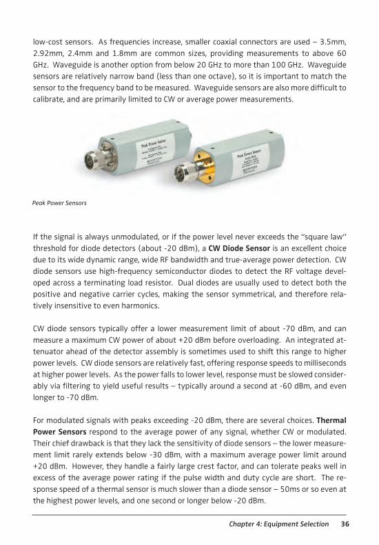
low-cost sensors. As frequencies increase, smaller coaxial connectors are used – 3.5mm, 2.92mm, 2.4mm and 1.8mm are common sizes, providing measurements to above 60 GHz. Waveguide is another option from below 20 GHz to more than 100 GHz. Waveguide sensors are relatively narrow band (less than one octave), so it is important to match the sensor to the frequency band to be measured. Waveguide sensors are also more difficult to calibrate, and are primarily limited to CW or average power measurements.
If the signal is always unmodulated, or if the power level never exceeds the “square law” threshold for diode detectors (about -20 dBm), a CW Diode Sensor is an excellent choice due to its wide dynamic range, wide RF bandwidth and true-average power detection. CW diode sensors use high-frequency semiconductor diodes to detect the RF voltage devel-oped across a terminating load resistor. Dual diodes are usually used to detect both the positive and negative carrier cycles, making the sensor symmetrical, and therefore rela-tively insensitive to even harmonics.
CW diode sensors typically offer a lower measurement limit of about -70 dBm, and can measure a maximum CW power of about +20 dBm before overloading. An integrated at-tenuator ahead of the detector assembly is sometimes used to shift this range to higher power levels. CW diode sensors are relatively fast, offering response speeds to milliseconds at higher power levels. As the power falls to lower level, response must be slowed consider-ably via filtering to yield useful results – typically around a second at -60 dBm, and even longer to -70 dBm.
For modulated signals with peaks exceeding -20 dBm, there are several choices. Thermal Power Sensors respond to the average power of any signal, whether CW or modulated. Their chief drawback is that they lack the sensitivity of diode sensors – the lower measure-ment limit rarely extends below -30 dBm, with a maximum average power limit around +20 dBm. However, they handle a fairly large crest factor, and can tolerate peaks well in excess of the average power rating if the pulse width and duty cycle are short. The re-sponse speed of a thermal sensor is much slower than a diode sensor – 50ms or so even at the highest power levels, and one second or longer below -20 dBm.
Peak Power Sensors

37
There are also Multipath Diode Sensors that integrate multiple diode detectors and at-tenuating power splitters into a single, calibrated unit. These operate several pairs of de-tectors (usually two or three), and select the output of whichever pair is operating in its square-law region. This has the effect of extending the true-average response of the diode sensor to much higher power levels – and yields a device which offers nearly the dynamic range of a CW diode sensor with close to a thermal sensor’s averaging ability. Drawbacks include cost, slow response and noise at certain power levels, and complications due to frequency and temperature correction differences between the detector pairs. Modern software techniques can minimize these last two issues.
Another solution for modulated signals is the Peak Power Sensor. These offer dynamic range between that of thermal sensors and CW diode sensors, but have extremely fast response speeds (microseconds or less). As long as this response speed (called “video bandwidth” and discussed in detail in Chapter 3 of this guide) is adequate, peak power sen-sor’s detector can faithfully follow the signal’s envelope modulation. This allows the sen-sor’s output to be accurately linearized and averaged by a high-speed sampler with suit-able software processing. Since peak sensors continuously yield the instantaneous power level of the signal’s envelope, a peak power meter can deliver more than just the average power. Burst (“time gated”) power, full waveform reconstruction, pulse profile and timing, peak power, and statistical power analysis are some of the more common measurements provided.
4.3 Selecting a Measurement ModeSome power meters can only handle specific types of sensors, while others offer consider-able flexibility. Sensors must be used with specific measurement modes in power meters that align with their capabilities:
• CW or Continuous Mode: this is the basic “continuous or free-run” mode used for CW power sensors. It returns average power of a CW signal, and will also return the aver- age power of a modulated signal with a thermal sensor or with a diode sensor operated within its square-law region. (see Figure 4.3.1 - Top)
• Modulated Mode: this is a more advanced “continuous or free-run” mode. It is similar to CW mode, but also returns limited peak information (peak, min, pk-avg ratio and dynamic range) when a peak power sensor is used. Also may be called “free-run” mode in peak power meters. (see Figure 4.3.1 - Top)
• Triggered or Pulse Mode: This mode is limited to peak power sensors. Typically itincludes full pulse profiling and time-domain measurements. A signal waveform is sometimes displayed, and the user can often select specific time intervals on the wave- form to measure. (see Figure 4.3.1 - Middle)

38Chapter 4: Equipment Selection
• Statistical Mode: This mode is limited to peak power sensors, and returns information about the signal’s statistical power distribution. Sometimes these measurements are performed as part of Modulated mode (for continuous statistical information), or as part of Pulse Mode (yielding synchronous or gated statistical information). (see Figure 4.3.1 - Bottom)
Measurement modes are discussed in more detail in Chapter 6 of this guide, but the follow-ing guidelines may be helpful for selecting the best power sensor and measurement mode for your signal.
Continuous (Modulated) Mode
Pulse (Trigger) Mode
Statistical Mode (CCDF)
Figure 4.3.1. Measurement Modes
39
Choose a CW Diode Sensor in CW Mode for these types of measurements:
• Thesignalhasalowpowerlevel,belowabout-40dBm.
• ThesignalisCW–asimple,unmodulatedRFcarrier.
• Youneedtomeasuretheaveragepowerofamodulatedsignalwhosepeaksdonot exceed the square-law threshold of a diode sensor (about -20 dBm).
Choose a Thermal Sensor in CW Mode for these types of measurements:
• Thesignal isCWormodulated,andhasanaveragepower levelthat isaboveabout -20 dBm.
• The signal contains a close-to-ideal pulse waveformwith a narrow duty cycle and peaks that would overload the square-law range of a CW diode or multipath sensor.
Choose a Peak Power Sensor in Modulated Mode for these types of measurements:
• Thesignalhasamoderatepowerlevel,aboveabout-40dBm.
• Thissignaliscontinuouslymodulatedwithavideo(AMorenvelope)bandwidthless than about 80 MHz.
• Signalmodulationmaybeperiodic,butonlynon-synchronousmeasurementsare needed (overall average and peak power).
• “Noise-like”digitallymodulatedsignalssuchasCDMAorOFDMwhenonlyaverage and peak power measurements are needed. (If peak probability information is required, consider Statistical Mode.)
Choose a Peak Power Sensor in Pulse Mode for these types of measurements:
• Periodic or pulse waveforms with pulse power above about -40 dBm. Pulses can be any shape.
• Bursted signals in which power measurement must be synchronized with the modulation.
• Anysortoftime-domainpowerprofileortime-gatedmeasurementisneeded.

40Chapter 4: Equipment Selection
Choose a Peak Power Sensor in Statistical Mode for these types of measurements:
• Thesignalhasamoderatepowerlevel,aboveabout-40dBm.
• “Noise-like” digitally modulated signals, such as CDMA (and all its extensions) or OFDM when probability information is helpful in analyzing the signal.
• Any modulated signal with random, infrequent peaks, when you need to know peak probability.
4.4 Measuring Complex Modulated RF Signal: Power Meters versus Spectrum Analyzers InstrumentsA number of RF and microwave power measuring instruments have been developed to measure a variety of signals for wireless communication, including cellular/mobile, and commercial and Government/military RADAR applications. For simplicity, these are divided into two categories: “tuned” and “broadband” measurement instruments.
A broadband or un-tuned power measurement uses a simple combination of a power de-tector and a display or recording instrument, while a tuned measurement is typically per-formed by a super-heterodyne, receiver-type circuit consisting of an input amplifier and/or attenuator, local oscillator, mixer, IF filters and amplifiers, and finally, a power detector or digitizing system. The basic receiver blocks can be combined to create instruments like Spectrum Analyzers, Microwave Receivers, Vector Signal Analyzers (VSAs), or Cellular Radio Test Sets.
For speed and accuracy over a wide bandwidth, the power detector/recording instrument (power sensor/meter) combination provides either the average, or modulated carrier pow-er of the RF signal at the input to the Sensor. Recent advances in sensor technology com-bined with improved computational capabilities using digital signal processing techniques allow the Power Sensor/Meter combination to quickly and accurately measure parameters including average power, peak and peak-to-average (PAR) power ratio, and time-domain profiles of complex digital modulation formats used in wireless communication systems. Although the Power Sensor/Meter instrument has no frequency selectivity, some new in-struments can provide time-slotted measurements and a large color display offering great detail for viewing the signal.
There are three typical detection circuits for modern power sensors, including thermistors, thermocouples, and diode detectors. Each type has specific advantages and limitations, and is discussed in detail in Chapter 2 of this guide.

41
For fast rise time and wide video BW peak measurements, the RF/microwave diode de-tector is often the best choice. The diode detector also excels where high sensitivity and wide dynamic range is required. Thermistor (bolometer) and thermocouple detectors can provide accurate, true average power measurements of both CW and wideband signals for calibration applications. (see Figure 4.4.1)
Unlike Power Meters, super-heterodyne type instruments, such as Spectrum Analyzers, of-fer frequency selectivity with limited bandwidth. These instruments are designed to per-form relatively narrow band power measurements while placing emphasis on the spectral power distribution. Recent progress in high speed digitizing and digital signal processing has improved the accuracy and functionality of these instruments for the measurement of digitally modulated signals. Some of the latest analyzers provide time-domain and statis-tical power analysis as well. (see Figure 4.4.2 and 4.4.3)
Uncertainty & Error SourcesThere are many sources of error and uncertainty when measuring the power of any RF signal, but these issues are further complicated by the wide bandwidth and dynamic range of complex modulated RF/Microwave signals. For CW signals, RF power meters are the accepted standards for accurate power measurement, but the choice is not so clear when modulation is added. In this case, there is a temptation to use a spectrum analyzer due to its ability to characterize the signal’s power distribution over frequency, but in addition to considerably higher cost, there are tradeoffs involved that can often reduce the measure-ment accuracy.
This section will explain why a Peak Power Meter is often the most cost effective choice for wideband, digitally modulated signals, offering unmatched speed and accuracy.
Accuracy is important for every test engineer, but there are many sources of error and uncertainty that contribute to inaccurate power measurements. It is essential when mak-ing measurements that errors and uncertainties are understood and either corrected, or accounted for to improve measurement accuracy.
In the RF Peak Power Meter, items contributing to errors include signal source mismatch, power reference and detector nonlinearity, calibration factor uncertainty, and instrumenta-tion noise and drift. Source mismatch errors are caused by impedance variation between the RF output of the signal source and the input of the power sensor. For most measure-ments, mismatch is the single largest source of error and maintaining the best possible match between the source and sensor will improve accuracy.
Sensor linearity is the next largest source of error for diode based Sensors used for most wide bandwidth and high dynamic range measurement requirements. Two diodes in a full-

42Chapter 4: Equipment Selection
wave rectifying arrangement are used to improve sensor linearity as shown in Figure 4.4.1. For signals below –20 dBm down to the sensor noise floor, the diode circuit has a linear response and requires minimal linearity correction. For signals above –20 dBm the sensor must use linearity correction techniques to compensate for diode nonlinearity.
Linearity correction tables for each RF power sensor are usually programmed into the sen-sor during factory calibration. These tables allow the instrument to display the correct power reading for all input levels, even though the sensor’s response may not be perfectly linear with applied power.
Vout
CL
RSource
RO
RO
VSource
CL
RL
RL
RTerm
Figure 4.4.1. Dual Diode RF Power Sensor Configuration
CRT
LocalOscillator
Mixer IF AmpLow Pass
Filter
EnvelopeDetectorRF Attenuator
RF Signal IF Filter
Ramp Generator for Sweep
X
Y
Figure 4.4.2. Typical front-end of a Superheterodyne Spectrum Analyzer

43
To correct for small sensor and meter response changes at the time of measurement, most high quality power meters include a built-in, traceable calibration source or precision power reference. Power sensor calibration methods are discussed in detail in Chapter 5 of this guide. The combination of factory and field calibration processes can generally provide the best correction for all types of sensor nonlinearities over the entire dynamic range of the instrument to minimize errors.
Figure 4.4.2 is a diagram of a basic analog spectrum analyzer. Like the power meter, this includes a power detector and measurement circuitry, but many additional components are necessary in a spectrum analyzer to provide the frequency-selective functionality. These additional components – attenuators, oscillators, mixers, filters and amplifiers all contrib-ute to the uncertainty of the power measurement performed by the instrument. Modern spectrum analyzers can significantly reduce errors by performing some of these functions digitally, discussed in detail below.
The incoming RF signal is typically applied to a wideband variable input attenuator to re-duce its amplitude to an acceptable level for the mixer stage that follows. Variable, or step attenuators rarely achieve excellent RF matching over a wide frequency range, so mis-match error will be the first uncertainty seen by the incoming signal. The step attenuator is characterized and calibrated for attenuation versus frequency at each attenuator setting, but there can still be a fair amount of uncertainty in this process.
Additional uncertainty is caused when switching between attenuator settings, since each setting presents a different input impedance to the user’s signal source. This results in a mismatch loss that is different for each attenuator setting. These mismatch loss varia-tions are calibrated out only if the complex source impedance of the signal being measured is the same as that of the calibration signal used for attenuator characterization. If the impedances are not identical, the actual mismatch loss at each attenuation setting will be different from the stored calibration value, and the power reading will change each time the attenuator range is changed.
Power meters do not have a narrow dynamic range mixer and do not require a step attenu-ator input. The RF signal source is applied to the power detector (and its built-in precision termination) either directly, or through a single, fixed attenuator. In addition to being able to maintain a very good match over a wide frequency range by removing the attenuator switching circuitry, the power sensor presents a fixed rather than variable termination to the RF source. While this does not eliminate mismatch loss, the loss remains constant over the full dynamic range of the signal, greatly improving power measurement linearity.
Power meters have additional accuracy benefits over spectrum analyzers because they do not have a heterodyne stage – the local oscillator, mixer and filter. All of these components

44Chapter 4: Equipment Selection
contribute to power measurement uncertainty. The mixer is a nonlinear device, and like a diode detector, its transfer function must be carefully characterized for frequency, am-plitude and temperature. A typical mixer has poor RF matching, but because it is isolated from the RF source by the input attenuator, the mixer’s poor match is only “seen” by the source at the analyzer’s most sensitive setting. The LO, IF and detector stages must be similarly characterized.
For the classic spectrum analyzer, the input attenuator, multiple frequency bands, local oscillators (LO), mixers, intermediate frequency (IF) amplifiers and filters (including the “RBW” filter) are all analog components, and contribute to uncertainty. Modern instru-ments implement some stages digitally reducing the uncertainly.
Depending upon the exact design, newer digital versions as illustrated in Figure 4.4.3 have similar attenuator and filter issues, but eliminate some LO and mixer issues. The digital process adds other sources of error including ADC quantization error, and sample and hold circuit jitter, but careful design can minimize or at least compensate for these effects.
The analyzer’s RBW filter may be adequate for a single frequency, continuous wave (CW) power measurement, but for digitally modulated wide band signals, portions of the chan-nel’s spectrum, as well as portions of the adjacent channel’s signal may or may not be excluded by the filter, reducing power measurement accuracy.
The level of measurement uncertainty is greater for a spectrum analyzer than a peak power meter because of additional measurement stages, but for many users this accuracy trad-eoff is offset by the additional functionality offered by the analyzer’s frequency selectivity.
ADC FFTInput
Attn SamplerLow Pass
FilterMicro-Processor
Display
f s
Figure 4.4.3. Digital FFT type Spectrum Analzyer

45
Benefits & Limitations of the Power MeterToday’s RF peak power meter is both fast and accurate, while providing true power mea-surements of the signal in the time domain. Whether pulsed RF or complex digitally modu-lated waveforms, the peak power meter is designed to accurately measure peak and aver-age power levels.
Complex modulated signals like code division multiple access (CDMA) are noise-like with random power peaks and require a statistical approach for proper measurement. Built-in digital signal processing capabilities allow the peak power meter to quickly perform statis-tical analysis on these complex signals.
The digital signal processing circuitry in Boonton peak power analyzers can continuously acquire and process power readings at sustained sample rates up to 25 MSa/sec and trig-gered burst rates of 50 MSa/sec. These measurements are quickly displayed in a statisti-cally meaningful probability density function (PDF), cumulative distribution function (CDF) or a complementary CDF (CCDF). These functions show the number of power measurement events at various levels (Figure 4.4.4.). The CDF and CCDF illustrate the fraction of time transmitter crest factor is above (or below) a desired level. This can show in time when the amplifier output is being clipped and compressed. This is useful during the design stage of the amplifier system for size and power requirements, or to take corrective action during operation of the amplifier to maintain optimum transmitter output power. Section 6.3 of this guide contains an in-depth discussion of statistical power analysis.
y+20 -
-30 -
-70 -
Wmax -
Wavg -
Powerdbm
0 pr1 50 100
PROBABILITY (%)
CCDF
Figure 4.4.4. Statistical occurrence of different power levels
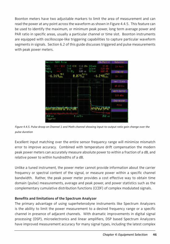
46Chapter 4: Equipment Selection
Boonton meters have two adjustable markers to limit the area of measurement and can read the power at any point across the waveform as shown in Figure 4.4.5. This feature can be used to identify the maximum, or minimum peak power, long term average power and PAR ratio in specific areas, usually a particular channel or time slot. Boonton instruments are equipped with oscilloscope-like triggering capabilities to capture particular waveform segments in signals. Section 6.2 of this guide discusses triggered and pulse measurements with peak power meters.
Excellent input matching over the entire sensor frequency range will minimize mismatch error to improve accuracy. Combined with temperature drift compensation the modern peak power meters can accurately measure absolute power to within a fraction of a dB, and relative power to within hundredths of a dB.
Unlike a tuned instrument, the power meter cannot provide information about the carrier frequency or spectral content of the signal, or measure power within a specific channel bandwidth. Rather, the peak power meter provides a cost effective way to obtain time domain (pulse) measurements, average and peak power, and power statistics such as the complementary cumulative distribution functions (CCDF) of complex modulated signals.
Benefits and limitations of the Spectrum AnalyzerThe primary advantage of using superheterodyne instruments like Spectrum Analyzers is the ability to limit the power measurement to a desired frequency range or a specific channel in presence of adjacent channels. With dramatic improvements in digital signal processing (DSP), microelectronics and linear amplifiers, DSP based Spectrum Analyzers have improved measurement accuracy for many signal types, including the latest complex
Figure 4.4.5. Pulse droop on Channel 1 and Math channel showing input-to-output ratio gain change over the
pulse duration

47
digital modulation formats. These units can display the waveform’s amplitude versus fre-quency in the band of interest, but the capability comes at a high cost, typically two to four times that of a high performance peak power meter.
However, the frequency tuning capability in a spectrum analyzer can be a hindrance when attempting to measure the power of a wideband signal. Figure 4.4.6 illustrates spectrum analyzer limitations using RBW filter settings narrower than the bandwidth of the signal, where power is added from the adjacent channel that will give an inaccurate reading. Be-cause the measurement is band limited, some noise power is excluded from the area of measurement to reduce accuracy.
In example (1) a CW signal can be ac-curately characterized with a swept or stationary center frequency and constant RBW setting.
In example (2), the RBW is too nar-row for the signal, so the center fre-quency must be swept and the power integrated to measure the total pow-er of the signal’s entire spectrum. This sweep results in a measurement time much greater than performing the same measurement with a peak power meter.
Example (3) shows a difficult mea-surement. The RBW cannot be made wide enough to encompass all three channels, but it is not narrow enough to totally exclude the adjacent chan-nels. Here, it will be necessary to use a very narrow RBW setting (and very slow sweep) to perform the mea-surement.
Figure 4.4.6. The accuracy of measurement is
dependent on the Spectrum Analyzer’s resolu-
tion bandwidth (RBW) filter
POWER
ƒ
POWER
ƒ
POWER
ƒ
Resolution BW (5 MHz)
10 MHz WiMax Signal
1.25 MHz WiMax Signal
5 MHz Resolution BW
1
2
3
CW
Resolution BW (5 MHz)

48Chapter 4: Equipment Selection
Magnitude accuracy is also reduced by sweeping the signal at high speed to capture fast transitioning signals. As a frequency domain instrument, it lacks the wide instantaneous dynamic range necessary to provide meaningful statistical data for a PDF, CDF, or a CCDF, vital information required for today’s complex digitally modulated communication signals.
SummaryDepending on the application, both broadband and tuned instruments are needed to mea-sure the power of complex RF and microwave signals.
For pulsed power applications like RADAR, the peak power meter is the clear choice for fast, accurate time domain measurements. Fast rise time, low duty cycle signals require a wide dynamic range to measure large peak to average power level differences.
For communication signals such as the noise-like modulation of a CDMA signal the peak power meter is an attractive proposition because of its wide dynamic range, wide video bandwidth, and statistical analysis capability.
When frequency or spectral information is not required, the RF Peak Power Meter provides the best combination of speed and accuracy over a wide range of frequencies, and at a price well below many Spectrum Analyzers. In contrast, the spectrum analyzer provides frequency content and selectivity that cannot be offered by power meters.
4.5 Oscilloscopes and Detectors Before modern peak power meters were available, a system that included a crystal de-tector, oscilloscope, average power meter, pulse generator and assorted couplers was as-sembled to capture pulse waveforms from high power amplifiers used for RADAR signals. Figure 4.5.1 is the block diagram of diode (crystal) detector system.
The CW input signal is connected to the pulse amplifier (DUT) input and pulse gated via the connected generator for a pulsed radar output signal. The signal is passed through a direc-tional coupler to either a dummy load, or actual antenna, and the crystal detector system. The test signal is then split between an average power meter, and a crystal (envelope) de-tector connected to the oscilloscope. The CW power meter will provide an absolute average power measurement, while the scope will provide the pulse envelope shape. The duty cycle is calculated by dividing the pulse repetition interval by the power envelope pulse width. The Pulse power is then calculated by dividing the average power value with the duty cycle measurement (see Figure 4.5.2).

49
This calculation assumes constant power during the pulse-on interval, a perfectly rectangu-lar pulse envelope, and a constant duty cycle. Errors frequently creep into the pulse power calculatino due to common pulse waveform anomalies like overshoot and ringing, or slow edge transitions. Figure 4.5.3 contains several examples of distorted pulse shapes.
pulse amplifier coupler load
pulse
generator
diodedetector
splitterpowermeter
oscilloscopepulse gate
Pulsed RF out
DUT
CW RF in
CW powersensor
Calibrated power value
Figure 4.5.1. Typical high power pulse power measurement system using conventional methods
Power EnvelopePulseRepetition
Interval(PRI)
PulseWidth(PW)
MeasuredAveragePower(pavg)
Duty Cycle = PW / PRIPulsed Power = Pavg / Duty Cycle
Figure 4.5.2. Relationships between Average Power, Pulse Power and Duty Cycle

50Chapter 4: Equipment Selection
Rise Time
Pulse
Power
Droop
Droop
Overshoot and
Undershoot
Figure 4.5.3. Distorted Pulse Waveforms
A modern peak power sensor and a crystal detector circuit are illustrated in Figure 4.5.4. The top figure is a typical single-ended detector circuit with uncertainty factors that in-clude an uncalibrated detector with limited dynamic range and a fairly high noise floor. The half wave rectified input cannot accurately measure asymmetretrical waveforms, and is af-fected by harmonic content. Matching to the RF source becomes difficult due to the parallel effect of the output load impedance. This load is necessary to achieve fast pulse response, and can either be the oscilloscope’s internal 50-ohm termination, or an external resistor. A portion of this impedance appears in parallel with the detector’s input termination, which affects the input VSWR. The effect is very small at low input levels, and becomes prou-nounced at high RF power inputs. Although the single ended detector can be calibrated using simple algorithms to improve the measurement, the dual diode differential sensor has several important advantages.
RF in
50 ohm diode
scope
diodedetector
RF in
50 ohmdual diodes
peak-detect
Half waveRectified
differentialpeak-detect
Full waveRectified
Figure 4.5.4. Typical Oscilloscope and Power Meter Detector Configurations

51
The differential system with two balanced diodes measures the fully rectified waveform.This improves linearity and measurement response time and cancels most waveform asym-metry for true signal envelope detection. The differential configuration reduces common mode noise, lowering the sensor noise floor while increasing dynamic range. Full-wave de-tection also significantly improves accuracy when measuring signals with high even har-monic content. Further improvements are made by accurately calibrating the sensor at several power levels spanning the sensors linear range (a diode detector’s square law re-gion). Modern instruments correct for non-linearity outside of that range, offering calibrat-ed measurements up to the detector’s power limit (see section 3.4 on Sensor Measurement Range). A modern two channel peak power meter offers the additional benefit of allowing simultaneous forward and reflected power measurements illustrated in the figure below.
In Figure 4.5.5, Channel 1 is the Radar output or reference signal and channel two is the return, or reflected power from the antenna. This value can be used to measure antenna efficiency (return loss, S11). The extra dynamic range provided by a calibrated dual diode sensor allows the user to measure forward and reflected power on the same instrument. In contrast, a traditional detector feeding an oscilloscope in conjunction with the average power meter limits dynamic range and requires splitting of the input signal to perform a single measurement.
The two channel peak power meter provides a simpler, more convenient method to mea-sure radar antenna return loss.
Radar ReceiverDirectionalCoupler
Reflected Signal RadarTransceiverAntenna
Radar Transmitter
Boonton 4500B
dc
dc Radar Signal
Figure 4.5.5. Power Meter Radar Antenna Return Loss Measurement

52Chapter 5: Calibration Issues
Chapter 5: Calibration Issues
Measurements are meaningless if they are not accurate, and even with the correct equip-ment, performing accurate power measurements requires a valid calibration. Power me-ters are faced with the task of delivering a precise power reading under varying conditions. The instrument and power sensor must both be calibrated so that the resulting power reading closely agrees with the actual RF input power, regardless of various instrumenta-tion and external variables.
This chapter discusses the linearity and frequency calibrations that are an integral part of the power measurement process. Most power meters also include temperature compensa-tion or correction – this is typically handled as part of the linearity correction process, and therefore is not discussed separately.
5.1 Factory Open-Loop CalibrationThe simplest calibration method dates back to early days of measurement, and involves applying known signal levels and physically marking the location of the indicator needle on the face of meter movement at each power step, then scribing a few marks between if needed. This creates a primitive “look-up table” which compensates for the gain and lin-earity (shape) of the transfer function of the combined sensor and power meter.
As time went on, the meter face markings became fixed, and adjustments were performed internally via a series of analog potentiometers, which could adjust gain and shaping for each of the power meter’s ranges. Nonlinear networks of diodes and resistors would allow moderately accurate correction for the curvature of the transfer function. In later years, discrete digital circuitry replaced these nonlinear networks for the “shaping” function. Again, this required that the sensor and meter be calibrated together as a unit.
Since most modern power meters are equipped to handle removable sensors, it now makes sense to calibrate the meter and sensor separately so that either can be interchanged with-out invalidating the calibration. To calibrate the power meter, it is connected to one or more precision DC reference voltages that simulate the output of a power sensor, and the meter is adjusted to standardized gain values across its operating range. This process is of-ten called DC calibration, and ensures that a particular sensor will produce the same reading on any calibrated power meter. It may take the form of a physical adjustment of analog po-tentiometers, or as a digital adjustment of gain and shaping coefficients through software.
But because every power sensor is different, a power meter must also know the precise re-lationship between the RF input amplitude and the detected output voltage from the con-nected sensor. This information can range from one or two numbers to multi-dimensional tables of calibration data. Information about the sensor’s transfer function can be charac-

53
terized at the factory, and stored in a nonvolatile EEPROM in the sensor. When the sensor is connected, this sensor calibration data is downloaded by the power meter and used as the basis for computing the proper RF power to display for a given output signal from the sensor. (see Figure 5.1.1)
Some power sensor types, such as thermocouple sensors, are very linear, producing an out-put voltage that is directly proportional to input RF power. CW diode sensors operating within the square-law region (below approximately -20 dBm) also share this characteristic. Linear power detectors like this are very simple to calibrate, and for some measurements all that is necessary is to store the “transfer gain” – just a single value of “microvolts per milliwatt” for moderate accuracy.
As the transfer function becomes nonlinear or increased accuracy is required, more complex equations are necessary to characterize the transfer function. Common techniques include polynomial curve fits of segments or the entire function. If calibration points are close enough together, even a second-order curve fit can produce excellent results.
5.2 Single, Double and Multipoint Linearity CalibrationsFor best possible accuracy in the field, many power meters include the ability to perform fine adjustments on the factory calibration by using a local reference level. There are three basic types of field adjustment:
• Single-point adjustment at zero input – referred to as a “Sensor Zero” or “null adjustment,” and still uses stored data to characterize detector and instrumentation gain and detector linearity (“shaping”). No RF reference is used.
• Twopointadjustmentatzeroinputandamid-orfull-scalepowerreference.Calibrate gain and offset, but still uses stored factory linearity data for transfer function shape.
• Multi-point adjustment at a series of power values. This process uses a series of power steps across the sensor’s full dynamic range to fully characterize the detector’s transfer function, and can replace or enhance the stored factory transfer function.
DUT
Detector Digitizer Linearizer Processor DisplayRF Amplifier
DC Signal
Amplifier
ADCPower Meter
Base UnitLCD
V in
P out
Figure 5.1.1. Signal Flow Block Diagram of sensor to meter to shaping to display

54Chapter 5: Calibration Issues
The zero adjustment is supported by nearly all instruments, and is necessary for perform-ing low-level power measurements. For best accuracy, a zero is typically performed im-mediately before any measurement in the lowest 10 dB or so of a sensor’s dynamic range. This minimizes the contribution of sensor drift and other phenomena which cannot be characterized in the sensor’s factory calibration. The zero adjustment usually just takes a highly-filtered reading over a relatively long time interval (often several seconds or more) and uses this value as an offset value. The stored factory transfer function is simply ad-justed up or down (offset) by the sensor zero.
The two-point adjustment consists of a sensor zero (offset adjustment) plus a gain ad-justment using a fixed power reference. Many power meters include a built-in 1.00 mW (0 dBm) RF reference output for this purpose. By adjusting the gain of the curve, small variations in attenuation due to sensor drift and aging, and connector wear can be com-pensated for. This process is sometimes called a “fixed cal,” and will affect all power values equally – by a fixed percentage in linear power (milliwatts), or by a constant number of dBm in logarithmic units. The stored factory transfer function is still used, but is adjusted for both slope and offset.
A multi-point adjustment further improves upon the adjustability permitted by zero and fixed cal adjustments. This field procedure is known as a “step cal” or “Auto-Cal” in Boon-ton power meters. Instruments that support step calibration replace the fixed 0 dBm pow-er reference with a precision power sweep calibrator that can generate precise, calibrated RF levels over a wide dynamic range. The calibrator is stepped through the sensor’s entire dynamic range, and a series of calibration values are stored for the exact connector/sen-sor/cable/instrument assembly in use, and at the current operating temperature.
Screen shot of “sensor zeroing”

55
Depending upon how many power steps are used for the calibration sweep, the factory transfer function can be adjusted at all points, or simply replaced. In either case, a number of uncertainties can be reduced or eliminated by “closing the loop” in the field, discussed more in the following section. Here are some common characteristics of performing a field step calibration:
• Providesbothgainandoffsetadjustment
• Fine-tunesthetransferfunctionoversensor’sentiredynamicrange
• Providesanimproved“currenttemperature”calibrationbeyondthefactory-character-ized compensation tables
• Compensatesfordetectoraginganddegradation(temporary,smalloverloads,ESDorphysical shock can cause slight changes to detector transfer functions)
• Compensatesforchanginglossesduetoconnectorwear
Sensor AutoCal sweep in progress

56Chapter 5: Calibration Issues
5.3 Field Linearity Calibration Methods All of the field linearity calibration methods discussed so far rely on the application of a known RF power reference to the sensor input to allow the sensor/power combination to yield the most accurate readings possible. However, when looking at the sources of poten-tial inaccuracy and drift, it should be apparent that there are a number of stages between the input RF signal and the digitized detector value, and all of these must be accounted for when the system is calibrated.
Traditionally, power meter base units and sensors are separately calibrated as discussed above in Section 5.1, and then the field calibration (zero, fixed cal, or step cal) is used to calibrate out the small errors that occur when a sensor is mated to a power meter, as dis-cussed in Section 5.2. The basic function of a power sensor is generally to convert RF power to DC voltage, while the function of a power meter is to convert that DC to a meaningful power reading.
The power sensor is factory characterized with one or more linearity tables that describe its transfer function, or in some cases, deviations from a stored “default” transfer function. Depending on the sensor, these tables may have multiple inputs to allow compensation for temperature and frequency, both of which can strongly affect the shape of the curve. But in all cases, the sensor’s calibration tables describe how its DC output (sometimes DC chopped to AC) relates to the RF input.
The power meter’s job is simple: measure the sensor’s DC output, and use the appropriate transfer function to linearize, or “shape” the value in milliwatts or dBm. This requires that the power meter know exactly what voltage the sensor is outputting, and this is where the calibration of the power meter base unit is required. Usually, this calibration is performed by connecting a precision DC source to the meter’s sensor input, and calibrating at one or more voltage points. This way, when the sensor is connected, the entire system will be in a calibrated state.
However, this process is not perfect – there can be small losses due to cables and con-nectors between the sensor and power meter, noise offset, as well as drift in the power meter’s analog stages. This drift and uncertainty is usually referred to as “instrumentation uncertainty” (see Chapter 9 of this guide), and will add to the drift and uncertainty of the detector itself.
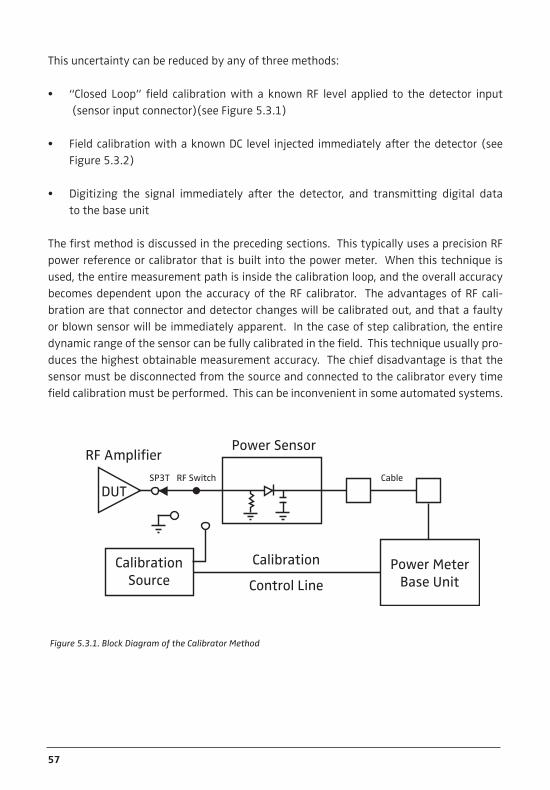
57
This uncertainty can be reduced by any of three methods:
• “Closed Loop”field calibrationwith a knownRF level applied to thedetector input (sensor input connector)(see Figure 5.3.1)
• FieldcalibrationwithaknownDC level injected immediatelyafterthedetector(seeFigure 5.3.2)
• Digitizing the signal immediately after the detector, and transmitting digital data to the base unit
The first method is discussed in the preceding sections. This typically uses a precision RF power reference or calibrator that is built into the power meter. When this technique is used, the entire measurement path is inside the calibration loop, and the overall accuracy becomes dependent upon the accuracy of the RF calibrator. The advantages of RF cali-bration are that connector and detector changes will be calibrated out, and that a faulty or blown sensor will be immediately apparent. In the case of step calibration, the entire dynamic range of the sensor can be fully calibrated in the field. This technique usually pro-duces the highest obtainable measurement accuracy. The chief disadvantage is that the sensor must be disconnected from the source and connected to the calibrator every time field calibration must be performed. This can be inconvenient in some automated systems.
DUT
Power SensorRF Amplifier
Power Meter
Base Unit
SP3T RF Switch Cable
Calibration
Source
Calibration
Control Line
Figure 5.3.1. Block Diagram of the Calibrator Method

58Chapter 5: Calibration Issues
The second method bypasses and disconnects the detector and injects a precision DC level into the signal chain in place of the detector output. This leaves the input connector and detector itself out of the calibration loop. However, since it is easier to generate a stable, precise DC voltage than an equally stable and precise RF power level, some of the uncer-tainty due to not calibrating the entire signal chain is offset by a reduction in uncertainty of the calibration source. The primary advantage of this arrangement is that the sensor can remain connected to the device under test during calibration. And of course, the dis-advantage is that drift or malfunction due to connector or detector aging or damage will go unnoticed. Since factory-generated linearity data must be used for shaping, detector linearity changes cannot be compensated for. This reduces accuracy somewhat compared to a closed-loop RF calibration.
The third method is used by most USB sensors, and reduces the need for field calibration because there are relatively few analog stages between the detector and the digitizer. When a digitizing sensor is factory calibrated, the entire analog signal chain is present, and since this circuitry is within the same housing and the sensor output is digital data, it is pos-sible to more accurately characterize the system at the factory. There are still errors that can crop up – not all USB ports deliver the same power supply voltage to the sensor, many are notorious for injecting large amounts of EMI which can cause false readings, and all the same RF problems exist (connector and detector aging or damage).
It is possible to combine techniques, and perform field linearity calibration on a digitizing sensor. Most allow (or require) at least a zero adjustment and the operating software often allows a fixed calibration using a known RF reference source. As of the publication date of this guide, there are no digitizing sensors that permit full power sweep field calibration, and all rely on stored factory linearity data.
DUT ADC
RF Amplifier Digitizer
Power Meter
Base Unit
Calibration
Control Line
DC Reference
Signal
DC Switch
SP3T
Figure 5.3.2. Block Diagram of DC Method

59
5.4 Frequency Response Correction The task of a power sensor is simple: convert RF to a measureable and known DC level across a broad range of carrier frequencies. However, detectors are not perfect, and there are always minor variations in the sensor’s output as frequency changes. Most sensors are fairly flat at lower frequencies, and begin to experience increasing response deviations as the input frequency goes up. Matching at the input RF connector and within the sensor’s detector assembly begin to play a role, and the output of the detector itself eventually falls off.
The good news is that the variation is generally small (typically no more than a few dB), and if the frequency is known, it is possible to compensate for the frequency response deviations. To accomplish this task, power sensors are factory calibrated at a series of fre-quency points to generate a table of correction values. These values are most commonly referred to as “Effective Efficiency” values (in percent), or “Calibration Factors” (in dB), and are supplied to the user.
In modern sensors, the table is stored in an EEPROM within the sensor, and the power meter can automatically load and apply the appropriate factor based on a user set frequency. If the operating frequency falls between table entries, an interpolation or curve fit is used. In some sensors, the frequency correction data is part of a multi-dimensional table that simultaneously performs linearity, frequency and temperature compensation.
There are two common methods of generating basic Calibration Factors. The first is a di-rect comparison with a “gold standard” power sensor that has a NIST traceable frequency calibration. In this technique, a leveled signal source is first swept or stepped through each desired calibration frequency, and the leveled power reading from the NIST traceable power sensor is recorded at each calibration frequency. That sensor is then replaced by the sensor to be calibrated, and the sweep is repeated. The ratio at each frequency point between the resulting reading and the corresponding reading from the reference sweep is the calibra-tion factor. (see Figure 5.4.1)
Setting frequency automatically computes the correct calfactor from sensor’s table

60Chapter 5: Calibration Issues
The second method uses a terminated average thermistor sensor (reference), precision power splitter, and a signal source. The generator supplies a CW signal at a specific frequen-cy to the precision power splitter and the reference power meter value is used to correct for any level variations from the signal source or splitter. (see Figure 5.4.2)
Power Meter
Base Unit
High Performance
Signal Generator
DUT
Power
Sensor
Power
Sensor
Calibration
StandardPrecision
Leveled
Signal
Figure 5.4.1. Diagram showing leveled source feeding first “standard” sensor, then DUT
PowerMeter
ReferencePower Meter
IEEE-488 Bus
Precision Power Splitter
High PerformanceSignal Generator
Power Sensor
DUT
Figure 5.4.2. Diagram of Power-Splitter based sensor frequency calibration setup

61
The center point of the splitter is a constant voltage point and the SWR at the splitter output port is dominated by that side arm of the splitter. Low splitter SWR minimizes mismatch error in the transfer of calibrations. In addition, the stability of the thermistor mount means that the combination can be accurately calibrated and will perform well with wide variations in generator characteristics. It also supplies transfer calibration factor ac-curacies of 1.2% to 2.5% (RSS) across the frequency range of the system.
The mistake that many customers make when attempting to perform their own transfer calibration comes from their belief that the output level of a signal generator is accurate and its VSWR is very good. The leveling accuracy of most generators is ±1 dB and VSWR rarely better than 1.35:1 over a broad frequency range. RF sweepers are even worse, of-ten having leveling inaccuracies of up to ±3 dB. That is why Calibration Factors cannot be checked by using just the output of a generator. They must be checked by one of the methods described above. Assembling and maintaining a traceable, automated sensor calibration station based on the power-splitter method is now within the reach of many calibration labs thanks to systems manufactured by Tegam.

62Chapter 6: RF Power Analysis
Chapter 6: RF Power Analysis
RF power measurement can be divided into several broad categories:
• Continuous Power Measurement. The measurement process is continuous or free-running, there are no pauses in acquisition and results are delivered as they are mea-sured. In almost all cases, the primary measurement is simply the average power. Other parameters such as peak power may also be measured.
• Triggered Pulse or Burst Acquisition. Typically the measurement process is discon-tinuous, and synchronized with the signal in some way. Once initiated, acquisition runs for a period of time then stops, and the result is delivered. The measurement result is generally a power-versus-time representation of the signal, and may include advanced time and power analysis.
• Statistical Power Analysis. A relatively new method of analyzing power in which a large population of power samples is acquired and analyzed to determine the frequen-cy of occurrence of a particular power level or range. The samples may be acquired continuously (free-run), or synchronized with the signal in some way (triggered or gated).
Following is a detailed discussion of each of these power measurement modes. All power meters support at least one of these methods, and more advanced peak power meters sup-port them all. Which mode is most appropriate will depend primarily on the signal being measured, but is also affected by what parameters of that signal are important to know.
Typical Modulated Mode displays

63
6.1 Continuous Power Measurement This is the most common power measurement method, and its operation can be likened to a digital multimeter. In the most basic continuous mode, the sensor is connected to a CW or modulated signal, and the power meter will simply display the average power of that signal. The display can either be numeric, with selectable resolution or graphical – most often displayed as a bargraph or meter scale. Units are most often dBm or watts.
CW and average diode sensors, thermal sensors and other types of low-bandwidth true-average power sensors all operate in continuous mode, often called “CW Mode” for these sensor types, since operation is tailored towards CW signals. Modulated signals may also be accommodated, but care must be taken to stay within the square-law region if a CW diode sensor is used. Modern instruments perform continuous mode measurements with a low-noise, low-bandwidth, high-resolution analog channel to process and digitize the sen-sor output, and all the shaping and corrections are performed by a microprocessor to yield an accurate power value.
Peak power sensors may also be used in continuous mode, sometimes referred to as “Mod-ulated Mode” since the peak sensor allows more flexibility and capability with modulated signals. The circuitry is somewhat different – a high-bandwidth amplifier and high-speed digitizer follow the detector, and the digitized samples are linearized and then averaged together to yield the average power. Additional parameters such as peak and minimum power can be made available with suitable processing. But the basic operating mode is the same – the power is continuously measured and displayed.
Continuous mode instruments generally measure power at a relatively slow rate – usually from about 10 Hz to a few kHz, and then apply a time integration filter to reduce noise further at low signal levels. This filter can also be useful for reducing the displayed power fluctuations caused by modulation. For periodic signals, it is beneficial to set the averag-ing time to be equal to an integer number of modulation cycles. Chapter 8 of this guide discusses the effects and benefits of signal filtering.
In addition to a numeric power display, continuous mode measurements may also be pre-sented in a graphical format showing power versus time, subject to the limitations of the measurement rate. Most useful is a “strip chart” type display, in which the power is shown as a scrolling line. In some instruments, this display can span from seconds to hours, which can be very useful for observing a drifting signal, especially when used in conjunction with appropriate signal filtering.
Another common feature of continuous mode measurements is ratiometric measurement. Most power meters allow the user to store a “reference level” from which a power ratio is computed and displayed. Most often the display is in dBr, with 0.00 dBr representing a

64Chapter 6: RF Power Analysis
power equal to the reference level. For dual-channel power meters, it is usually possible to display the ratio between the two channels as well. This can be useful for computing gain or attenuation. When used with a directional coupler, the ratio between the channels is equal to the return loss of the signal passing through the coupler.
The primary display may be the actual sensor signal amplitude, offset amplitude, or a mathematical function (ratio, sum or difference) of the sensor signal and the signal from a second sensor or stored reference.
6.2 Triggered and Pulse Analysis For periodic or pulsed signals, it is often necessary to analyze the power for a portion of the waveform, or a certain region of a pulse or pulse burst. The following is a brief review of power measurement fundamentals:
Unmodulated Carrier Power. The average power of an unmodulated carrier consisting of a continuous, constant amplitude sinewave signal is also termed CW power. For a known valueofloadimpedanceZLOAD, and applied voltage VRMS, the average power is:
P = VRMS² / ZLOAD watts
Power meters designed to measure CW power can use thermoelectric detectors which re-spond to the heating effect of the signal or diode detectors which respond to the RMS volt-age of the signal. With careful calibration, accurate measurements can be obtained over a wide range of input power levels.
Modulated Carrier Power. The average power of a modulated carrier which has varying amplitude can be measured accurately by an average or CW type power meter with a ther-moelectric detector, but the lack of sensitivity will limit the range. Diode detectors can be used at low power levels that are within the square-law response region (no peaks higher than about -20 dBm). At higher power levels the diode responds proportionally to voltage rather than power, and significant error in the average power reading will result.
Pulse Power. Pulse power refers to power measured during the on time of pulsed RF sig-nals (see Figure 6.2.1). Traditionally, these signals have been measured in two steps: (1) average-responding sensors (thermoelectric or square-law diode types) measure the aver-age signal power, (2) the average reading is then divided by the duty cycle to obtain pulse power, PPULSE :
PPULSE = PAVERAGE / Duty Cycle where Duty Cycle = Pulse Width / Pulse Period

65
Pulse power computed in this way provides useful results when applied to ideal, periodic, rectangular pulse waveforms, but is inaccurate for pulse shapes that include distortions, such as overshoot or droop, or if pulse period and width are not perfectly uniform. (see Figure 6.2.1)
Peak Power. Peak power meters perform power measurements in a manner which over-comes the limitations of the pulse power method and provides both peak power and aver-age power readings for all types of modulated carriers. Fast responding diode detectors track the RF envelope to produce a wideband video signal which is sampled at a high band-width and data rate by the peak power meter. The sampled detector points are accurately converted to instantaneous power in watts on an individual basis using stored calibration information.
Once the samples have been converted to linear power, the mean value of all or a subset may be computed to yield the true average power without restriction to the diode detec-tor’s square-law region. A time-domain reconstruction of the signal’s envelope can be cre-ated by assembling the samples in sequence into a display buffer. For repetitive signals, this process can make use of equivalent time or interleaved sampling techniques to yield time resolutions greatly exceeding the sample rate when synchronized by an internal or ex-
v(t)
t
v(t)
t
(a)
(b)
Figure 6.2.1. Ideal (a) and distorted (b) pulsed RF signals

66Chapter 6: RF Power Analysis
ternal trigger signal. Repetitive signals also permit synchronous filtering (trace, or “video” filtering) of the resulting waveform – discussed in more detail below.
Peak power meters often refer to this measurement mode as “Triggered” or “Pulse Mode”. Operation is similar to a modern digital storage oscilloscope – power samples are stored in a circular memory buffer until a trigger signal is received. The samples, with the desired re-lationship to the trigger signal, are then selected and processed to obtain a power-versus-time trace.
The trigger signal can either be a separately applied “external” pulse, or can be generated by the RF signal’s amplitude crossing a defined threshold in either direction. The trigger source, level and polarity are programmable, and oscilloscope-like settings such as trigger delay time and trigger holdoff are often available.
Early peak power meters did not have memory – they used a variable delay generator, and sampled the input signal at some defined period after the trigger to yield “power at a time offset”. To reconstruct the waveform, the delay time was incremented in small steps in each succeeding trigger, and the resulting array of power points assembled in order on a display. This technique permitted wide measurement bandwidth using the slow A/D con-verters of that time period.
Modern peak power meters acquire the signal at very high conversion rates – typically many MHz – and large acquisition buffers permit display of both pre- and post-trigger por-tions of the waveform. For each triggered sweep, data acquisition into the circular buffer is restarted, and it runs at high speed until a trigger edge has been detected and all post-trigger samples acquired. At this point, acquisition stops, using the buffer is processed and displayed before another trace is restarted.
Rising edge of a Peak Power Envelope

67
Triggering. Like a DSO, there are a number of trigger options. Auto-trigger modes will force a trigger when no edges are detected, but will synchronize with the signal once the edges appear. A “peak-to-peak” trigger mode can be chosen to automatically set the trig-ger level based on the input signal. The most advanced peak power meters have complex trigger generators which can do trigger arming and qualification on counted signal events or time delays. Some also have programmable “fence” and exclusion intervals to assist triggering on burst type signals.
Display timebases range down to the few ns/div range, limited generally by the video bandwidth and time resolution of the instrument. Time resolutions of 200ps or better are available on the fastest peak power meters, and are critical to accurate waveform recon-struction and pulse measurement. (see Figure 6.2.2)
Programmable time markers (cursors) are often available, and may be positioned on any portion of the displayed trace to mark regions of interest for detailed power analysis. Cur-sor measurements generally include the power at each marker, as well as a series of param-eters for the interval defined between the two markers – usually at least the average and peak power. This is very useful for examining the power during a RADAR pulse or digital communication burst when only the central region of the pulse is of interest. By adjusting trigger delay and other parameters, it is possible to measure the power of specific timeslots of TDMA signals such as GSM and EDGE.
Trigger holdoff allows burst synchronization even if there is more than one edge in the burst which may satisfy the trigger level. Simply set the holdoff time to slightly shorter than the burst’s repetition interval to guarantee that triggering occurs at the same point in the burst each sweep.
Figure 6.2.2. Screen shot of under-sampled rising edge on left and well-defined, over-sampled edge on right

68Chapter 6: RF Power Analysis
For periodic waveforms, automatic measurement of waveform parameters is available in pulse mode. Once a stable, periodic signal is detected, the instrument automatically lo-cates the waveform transitions, and calculates a number of pulse parameters such as pulse frequency, width, duty-cycle, rise and fall times, top and bottom powers, pulse on power, overshoot, and average power a full cycle.
Trace averaging is available, and generally required for performing low-level measurements due to the wideband noise of peak power sensors. Unlike Continuous Mode, in which the measurement bandwidth is simply reduced by averaging more samples, Pulse Mode uses synchronous averaging, or “Video Averaging”. This averages each acquisition sample with other samples at exactly the same time offset relative to the trigger, effectively averaging each trace with the previous traces while maintaining time alignment. Video averaging works best for periodic waveforms. A detailed description of this process and its benefits is discussed in Chapter 8 of this guide.
Pulse mode of advanced peak power meters often include the same sorts of features found in advanced digital oscilloscopes including deep memory, waveform zoom, trace storage and recall, and mathematical functions between traces.
6.3 Statistical Power Analysis For pulsed and periodic waveforms, the signal’s power envelope can be reconstructed and analyzed in the time domain to provide a considerable amount of useful information. However for continuously-modulated signals or periodic signals with noise-like modulation within bursts or packets, it becomes difficult or impossible to trigger from the signal itself, or to extract useful information in the time domain. Simple, continuous-mode processing can yield the average and sometimes peak power, but often there is more information to be gained by alternate acquisition and processing methods.
Figure 6.2.3. Screen shots showing cursor measurements and statistical distributions
69
Many modern communication signals fall into this category due to their noise-like, digi-tally modulated data formats; CDMA, OFDM and various forms of QAM are some examples. For these signals, statistical power analysis often makes more sense than time-domain analysis. When statistical analysis is performed, power samples are acquired and analyzed by how frequently each power value occurs rather than precisely when it occurs. A large sample population is acquired either asynchronously or synchronously, and then sorted by power into “bins” to yield a histogram. The more samples in the population, the finer the histogram resolution.
Statistical Power Analysis is best for signals with the following characteristics:
• Moderatesignallevelaboveabout-40dBm.
• Digitally modulated signals, especially “noise like” formats such as CDMA (and its extensions) or OFDM when probability information is helpful in analyzing the signal.
• Anysignalwithrandom,infrequentpeaks,whenyouneedtoknowpeakprobability.
Statistical Presentations. There are several common presentations for viewing statistical power measurements: Histogram, PDF, CDF and CCDF are a few viewing options for each.
• Apower histogram is the simplest – the samples are sorted into equal-width bins of any convenient size. The bin divisions are most often logarithmic in power, with each bin ranging an equal number of dBm. Bin depths (maximum count values) can be up to or exceeding 32 bits (4 billion counts).
• ThePDF,orProbability Density Function is essentially a continuous function that is similar to an infinite-resolution (zero bin width) histogram. The PDF cannot directly re-turn absolute signal measurements, but its shape yields a qualitative indication of the power distribution. A multi-level signal such as QAM will show up as a distinct “hump” at each power level, and may be useful for visualizing system linearity.
• The CDF, orCumulative Distribution Function is the integral of the PDF. Its value is monotonic and increases from 0.0 to 1.0, and represents the probability that the power is at or below that point. Textbook representations will have the independent variable (in this case power) on the X axis and probability on the Y axis. A CDF value of 0.0 will be found at the minimum power point, and a CDF value of 1.0 will be at the maximum (absolute peak) power.

70Chapter 6: RF Power Analysis
• TheCCDF,orComplementary Cumulative Distribution Function (sometimes shown as “1-CDF”) is simply the arithmetic inverse of the CDF, representing the probability that the power is at or above that point. A CCDF value of 0.0 will be found at the maxi-mum power point, and a CCDF value of 1.0 will be at the minimum power. The CCDF presentation is more often used for power analysis because peak power is generally of more interest than the minimum power, and it is more convenient to expand about the origin.
Frequent Events
IncreasingProbability
Infrequent Events
Increasing Crest Factor
Normalized CCDF plot showing probability on the Y axis versus normalized power on the X axis (dual channel overlay)
CDF
Increasing Occurrence0% 100%
Amplitude
15.8 dBm
Amplitude
Decreasing Occurrence0% 100%-3.6 dBm
3 dBm
12.2 dBm
CCDF
Figure 7.2.3. Common statistical diagrams including a PDF, CDF and CCDF

71
The CCDF is most often presented graphically using a log-log format, with log power (dBm) on the X axis and log probability on the Y axis. For analyzing communication signals, it may be helpful to normalize the power to the average power, so the X axis represents the number of dB above or below the average power level (now scaled in relative dB, or dBr). This is useful because it is sometimes only the shape of the CCDF that is important, and not its absolute power value. In this case, a power value of 0 dBr is the average power, and a CCDF value of 0.0 represents the peak-to-average power ratio.
Some power meters invert the X and Y axes to maintain the power measurement conven-tion of displaying amplitude on the Y axis. This can be particularly useful when presenting a histogram or PDF along with a corresponding time-domain trace. Both orientations present the same information.
4500B gated histogram with power on the Y axis. Pulse waveform in upper windows showing time gate cursors,
and gated PDF (high resolution histogram) in lower window. For this view, it is more meaningful to present power
on the Y axis using the same scaling in both windows.
Figure 6.3.1. Tabular CCDF view
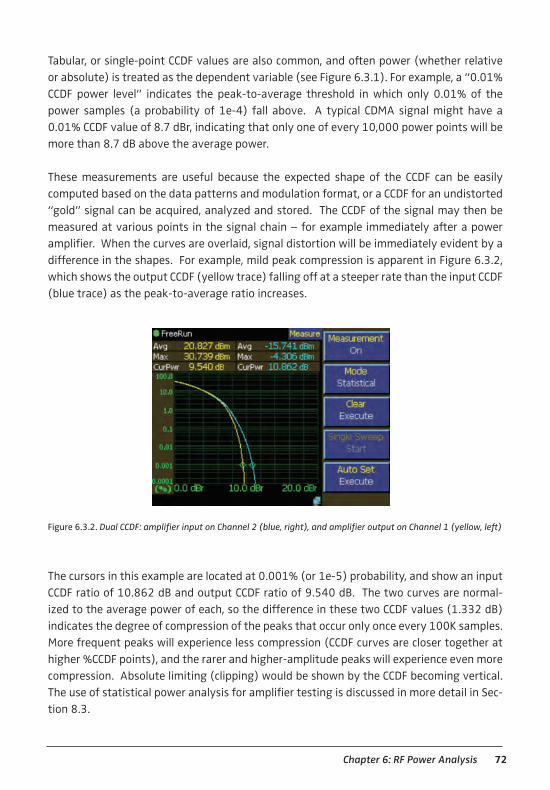
72Chapter 6: RF Power Analysis
Tabular, or single-point CCDF values are also common, and often power (whether relative or absolute) is treated as the dependent variable (see Figure 6.3.1). For example, a “0.01% CCDF power level” indicates the peak-to-average threshold in which only 0.01% of the power samples (a probability of 1e-4) fall above. A typical CDMA signal might have a 0.01% CCDF value of 8.7 dBr, indicating that only one of every 10,000 power points will be more than 8.7 dB above the average power.
These measurements are useful because the expected shape of the CCDF can be easily computed based on the data patterns and modulation format, or a CCDF for an undistorted “gold” signal can be acquired, analyzed and stored. The CCDF of the signal may then be measured at various points in the signal chain – for example immediately after a power amplifier. When the curves are overlaid, signal distortion will be immediately evident by a difference in the shapes. For example, mild peak compression is apparent in Figure 6.3.2, which shows the output CCDF (yellow trace) falling off at a steeper rate than the input CCDF (blue trace) as the peak-to-average ratio increases.
The cursors in this example are located at 0.001% (or 1e-5) probability, and show an input CCDF ratio of 10.862 dB and output CCDF ratio of 9.540 dB. The two curves are normal-ized to the average power of each, so the difference in these two CCDF values (1.332 dB) indicates the degree of compression of the peaks that occur only once every 100K samples. More frequent peaks will experience less compression (CCDF curves are closer together at higher %CCDF points), and the rarer and higher-amplitude peaks will experience even more compression. Absolute limiting (clipping) would be shown by the CCDF becoming vertical. The use of statistical power analysis for amplifier testing is discussed in more detail in Sec-tion 8.3.
Figure 6.3.2. Dual CCDF: amplifier input on Channel 2 (blue, right), and amplifier output on Channel 1 (yellow, left)

73
Gated statistics. Many modern signals are transmitted in bursts or timeslots, but also use noise-like digital modulation formats that will benefit from statistical analysis. For these protocols, it is beneficial to acquire the statistical population synchronously – that is trig-gered or gated externally or by the signal so that the acquired samples only represent par-ticular intervals in time. GSM-EDGE is one example – it is most useful to acquire data only during the payload portion of the timeslot. WiFi and other signals have similar require-ments – often a burst begins with some sort of training sequence that will skew the dis-tribution in undesirable ways if samples from that interval are included in the population. (see Figure 6.3.3)
High-end peak power analyzers offer the ability to operate in two modes simultaneously. The instrument is set up for a basic, pulse mode acquisition so that a triggered waveform is visible. All triggering features of the power meter may be used. Cursors are then po-sitioned on the waveform to indicate the interval over which to perform statistical analy-sis. Only power samples occurring within this interval are included in the population. All samples outside the interval, such as the burst “off” time, rising and falling edges, and data references such as pilots and training sequences are discarded, and will not skew the distribution.
Statistical Acquisition Size. One weakness of statistical power analysis is that the power bins used to acquire data are not of infinite depth. The faster the data points are acquired, the sooner the bins will fill up, and eventually the maximum count limit is reached and ac-quisition can no longer proceed. At this point, a decision must be made on how to handle the situation. (see Figure 6.3.4)
Figure 6.3.3. 4500B screen shot of Gated CCDF showing the pulse waveform of a WLAN frame, and time gates in
the upper window, and the signal’s CCDF curve in the lower window. The time gates in this example have been po-
sitioned to include only the payload portion of a data frame, and exclude the interval that the pulse is off, as well
as its initial training sequence.

74Chapter 6: RF Power Analysis
The simplest option is to consider the acquisition “complete” and stop adding new samples to the population. Depending whether statistical measurements will be immediately re-quired, it may be more appropriate to clear the population and restart acquisition of a new population. The down side of this “flush and restart” technique is that there is a short pe-riod at the start of each acquisition when the population is small and the statistical resolu-tion will be extremely coarse. If a CCDF measurement at a very small probability is needed, there may not be enough samples for a statistically valid return value.
To remedy this, a portion of the distribution may be discarded, or “decimated”. All power bins are scaled by an equal value, for example 0.5. This is computationally simple, and fast to perform – the binary count values in each bin are right shifted by one bit. Once all the count bins have been halved, acquisition can continue. The elegance of this technique is that the shape of the statistical distribution is not affected except at the very rarest power values, where binary roundoff error or truncation becomes significant.
The effect can be considered a CCDF “filter,” in which the distribution is most heavily weighted by recent events, and older events eventually are decimated off the bottom. The time it takes this to happen is proportional to the count at which decimation occurs, and inversely proportional to the sample rate.
Many signals can yield meaningful CCDF results with several to a few tens of megasamples, so it is possible to make use of this decimation process for less than a “full” bin. Peak pow-er meters may include the option to terminate, restart or decimate statistical acquisition after a user-defined population size (“Terminal Count”) or time interval (“Terminal Time”) has been reached. (see Figure 6.3.4)
Figure 6.3.4. Terminal count options

75
Chapter 7: Power Measurement Applications
This chapter discusses several common power measurement applications:
• LowDutyCycleMeasurements – a discussion of why the conventional AveragePower / DutyCycle method for computing pulse power is inaccurate for narrow duty cycle waveforms, and the advantages of using peak power measurement techniques. (see Figure 7.1.4)
• MeasuringModernCommunicationSignals – considers the special needs when mea-suring digitally-modulated signals of modern wireless networks. The modulation for-mats used often require special techniques to yield accurate and meaningful results.
• Using Power Meters for EMC Testing – EMC testing is receiving a great deal of atten-tion. RF emissions are, and have always been important, but increasing emphasis is now being placed on equipment’s immunity from various types of interference. As the signals used for EMC testing have become more complex, traditional methods of in-strumenting the test environment and test results have given way to new techniques requiring the use of peak power measurements.
7.1 Low Duty-Cycle Pulse Measurements Why the average power measurement is not adequate! A prime concern for specialized tube amplifiers like TWTA’s, magnetrons, and klystrons is the amplitude, quality and sta-bility of the device’s output power. These devices are designed for high power RADAR, particle accelerators, and Magnetic Resonance Imaging devices (MRI). They must provide consistent pulsed linear power to either a large antenna with low return loss, or to large powerful magnets that create similar power transfer issues. These amplifiers require ac-curate peak power measurement for safety and optimum performance. A common charac-teristic of these applications is the use of a low duty cycle pulse for measuring a small size at a far distance for radar applications, or accurately controlling atom size particle position for physics research.
Before peak power meters were available, the pulse power was computed indirectly from an average power measurement performed with an average-responding power meter. The pulse power was calculated by dividing the average power (PAVG) by the duty cycle. The duty cycle is often a known characteristic and is calculated by dividing the pulse width of the power envelope by the pulse repetition interval. (see Figure A 7.1.1)

76Chapter 7: Power Measurement Applications
Rise Time
Pulse
Power
Droop
Droop
Overshoot and
Undershoot
Figure 7.1.2. Common pulse waveform distortions that can affect the accuracy of pulse power computations
Power Envelope
RF Carrier
Figure 7.1.3. Envelope of a wide duty cycle pulse waveform is simple to measure with most average-responding
power meters
PulseWidth(PW)
MeasuredAveragePower(Pavg)
Power envelopePulse
RepetitionInterval
(PRI)
Duty Cycle = PW / PRIPulsed Power = Pavg / Duty Cycle
Figure 7.1.1. Pulse Power Computation
This computation assumes constant peak power and does not take into consideration fac-tors such as overshoot and ringing. This is why it is called pulse power and not peak pulse power (see Figure 7.1.2). The pulse must be repetitive, rectangular, and of constant duty cycle to make an accurate calculation. For more information on this topic see Section 4.5.

77
One advantage of using an average power meter is the ability to measure over a wider dynamic range than a peak power meter, but this assumes the signal envelope is a perfect rectangle. This advantage disappears for narrow duty cycle signals. (see Figure 7.1.3)
In a RADAR or MRI system, the RF or microwave carrier is sent in short bursts over long periods to provide a signal to measure over long range and small object size. Simple range finding radars use pulse modulation, while some doppler radars use a continuous wave tone. Pulse modulation requires the carrier to be switched on and off in synchronization with an external pulse signal and is not modulated like a communication signal. The enve-lope of the pulse waveform is extracted from the demodulated carrier in the receiver (see Figure 7.1.3).
A CW signal has the same average and peak power value and can be measured provided the value is within the sensors dynamic range. A narrow duty-cycle pulsed signal can have a significantly lower average value outside of the sensors dynamic range which the peak value falls within that range.
To perform an accurate measurement of pulse power using the duty cycle method, it is necessary to accurately measure the signal’s average power. This requires maintaining the average power well above the sensor’s noise floor. At the same time, the power sensor must be able to handle the highest power peaks while the pulse is on, or the sensor will produce erroneous readings or burn out.
Most average power sensors can accommodate peaks that are 10 dB to 20 dB above their maximum average power ratings, so pulse waveforms with relatively wide duty cycles can be measured without challenge (see Figure 7.1.3). But for signals with duty cycles narrow-er than about 1%, the dynamic range of the average-responding power sensor is eroded by the need to maintain both the peak power and the average power within the sensor’s operating, and measureable range.
Duty Cycle = 0.001%
100ms
1us
Figure 7.1.4. Narrow Duty Cycle pulse envelope
78Chapter 7: Power Measurement Applications
Simply stated: As the duty cycle of a power envelope is decreased, typically below 1%, the average power reading is further away from the actual peak power delivered and requires larger dynamic range sensors. (see Figure 7.1.4)
The following example, calculation shows duty cycle and dynamic range computations for a periodic waveform with a one microsecond pulse repeating at a 10 Hz rate.
Duty cycle calculation: (1.0e-6 / 0.1) = 0.00001, or 0.001%
Conversion to dB = 10 x Log10(0.00001) = -50 dB
Therefore, measuring the pulse power of this signal requires a power meter with at least 50 dB of dynamic range. For a typical thermal sensor with 22 dB peak headroom (+42 dBm), this means the signal’s average power must remain at least 50 dB below its peak rating, or -8 dBm. These types of sensors have a noise floor of about -25 dBm, so the signal can vary by no more than 17 dB before its peak burns out the sensor or its average falls below the noise floor. For accurate measurements, the signal should remain 6 to 10 dB above the noise floor, further degrading the dynamic range.
A peak power sensor with its wide dynamic range is often a better solution for measuring this type of signal for several reasons.
1. The pulse shape is not always rectangular and will contribute errors when calculated using an average power sensor measurement in the pulse power calculation.
2. The dynamic range of an average power sensor is reduced in proportion to the duty cycle because the noise is integrated into the measurement with a long PRI and a short pulse width.
3. A fully calibrated good quality peak sensor has a dynamic range of 70 dB and capable of measuring a 50 dB peak to average ratio without affecting the measurement.
Figure 7.1.5 shows a comparison of Duty Cycle vs. Peak Pulse Power for three common power sensor types. The sensors used for this comparison are an average-responding ther-mocouple sensor, an average-responding diode sensor (operating in the diode’s square-law region below -20 dBm), and a peak power diode sensor. The maximum and minimum power values for each sensor represent their total dynamic range capability.

79
Note for the two average-responding sensors, that the usable dynamic range becomes narrower as the duty cycle decreases. However, this is not the case for the peak sensor. Although it can handle short peaks up to 10 dB above its +20 dBm average power rating, its measureable pulse power rating does not rise with narrowing duty cycle due to the +20 dBm upper limit of its calibrated measurement range. But on the lower side, the noise floor does not increase as the duty cycle narrows because the peak sensor is able to trigger and measure only during the “on” portion of the pulse, and discard measurements at all other points in time.
This means that the usable dynamic range of a peak power sensor remains constant with duty cycle, unlike average responding sensors. The pulse waveform in our example above can be measured while the signal varies over a 60 dB dynamic range, and still remain sub-stantially above the sensor’s noise floor to produce stable and accurate measurements.
The shading of Figure 7.1.5 provides additional insight into how the available dynamic range of average-responding sensors is reduced when measuring narrow duty pulses. This is shown in Figure 7.1.6.
Note that both thermal and average diode sensors run out of dynamic range for duty cycles narrower than about 0.003%. The operating area of the thermal sensor can be extended in some applications by taking advantage of the fact that its peak handling capability is con-siderably higher than its average power rating. This is dangerous, however, as the source
Thermal, Average Diode, and Peak Power Comparison50
40
30
20
10
0
-10
-20
-30
-40
-50
-60
-70
100 10 1 0.1 0.01 0.001 0.0001 0.00001
Peak
Pul
se P
ower
(dBm
)
Duty Cycle (%)
Thermal Detector Power Limit
Thermal Detector Noise Floor
Uncalibrated Diode Detector
Power Limit
Uncalibrated Diode Detector
Noise Floor
Peak Sensor Noise Floor
Peak Sensor Power Limit
Figure 7.1.5. Thermal, Average Diode, and Peak Power comparison

80Chapter 7: Power Measurement Applications
may be able to generate considerably more power than the sensor can safely handle. The user must depend upon the signal’s duty cycle remaining narrow enough to limit the av-erage power to a safe value. If the signal’s duty cycle increases, the average power will increase accordingly.
The peak power sensor does not suffer from duty-cycle limitations, and its operating dy-namic range is wide no matter what the waveform’s duty cycle. The true peak power of the signal is measured directly, and even single pulse events may be easily measured.
7.2 Statistical Analysis of Modern Communication Signals The latest wireless communication formats like DVB, DAB, WiMax, WLAN, and LTE cellular use OFDM modulation schemes with multiple carriers to transmit digital information. OFDM is a multi-carrier modulation scheme with a high crest factor to transmit large amounts of data. The introduction of digital transmission technology has made it necessary to deal with power peaks up to 20 dB above the average value. RF power components must be suitably specified to handle the expected voltage peaks and avoid break down, or flash over. The crest factor, i.e. the ratio of the peak value to the average or RMS value, must be determined to correctly specify these components. The peak power of several intercon-nected transmitters can reach more than one hundred times the thermal or average power level. The selection of the RF power components for the transmission system (antenna combiners, coaxial lines and antennas) cannot be based solely on the thermal or average power. Short voltage spikes that occur rarely are critical when determining the required size and power handling capability of the RF components.
50
40
30
20
10
0
-10
-20
-30
-40
-50
-60
-70100 10 1 0.1 0.01 0.001 0.0001 0.00001
Peak
Pul
se P
ower
(dBm
)
Duty Cycle (%)
Thermal Sensor“Extended” Area
Peak Power SensorDynamic Range
Avg Diode SensorDynamic Range
Figure 7.1.6. Dynamic range of Thermal, Average Diode and Peak Power sensors versus duty cycle

81
Crest factor measurements over 12 dB (PPEP/PAVG) are difficult to make with repeatable re-sults. To properly accommodate for these high crest factors a single peak measurement is not adequate and statistical analysis should be used. Low amplitude communication signals with high crest factor, although important when considering BER, are of greater concern for their contribution to system damage. The high voltage associated with large power peaks can produce flashover, or a standing arc in the transmitter system and de-stroy components. Statistics are an important tool for measuring these rare events when concerned with property and personal damage. Because the instantaneous power values are sorted by magnitude rather than their time of occurrence, they are counted and not averaged. This process can run for a very long time, limited only by available memory, or can run indefinitely if decimation is applied. It is invaluable for characterizing events, such as the maximum peak power of an OFDM signal that might occur once a day. Capturing pulse data using statistics provides additional insights not easily observed when capturing amplitude vs. time measurements.
Figure 7.2.1 shows a real world CCDF (complementary cumulative distribution function) of an HDTV, OFDM modulated signal. Trace A shows a 100% AM modulated sine wave, which has “squared off” CCDF showing a peak-to-average ratio of 3 dB at both low and high prob-abilities. This is due to the highly predictable periodic waveform. The OFDM signal shown in Trace B has a peak-to-average ratio of about 15dB, and follows a Rayleigh distribution pattern. Trace C shows white, Gaussian noise for reference, which has a theoretically infi-nite peak-to-average ratio, here shown to be about 17 dB for at a probability level of 10-12.
0 2 4 6 8 10 12 14 16 18 20
100
10-2
10-4
10-6
10-8
10-10
10-12
10-14
A B C
k in dB above average
prob
abili
ty p
A = CCDF of sine-wave B = OFDM envelope C = white noise
Figure 7.2.1. CCDF of a sinusoidal signal (carrier approach), an OFDM envelope signal and for white noise

82Chapter 7: Power Measurement Applications
For the AM modulated signal, it is clear that very few samples must be acquired to measure the signal’s peak power, while the digital OFDM signal has a high peak-to-average ratio with peaks that occur very infrequently. For these types of signals, the power meter must acquire many samples over a period of time to accurately characterize the power distribu-tion of the signal.
The following section will explain the statistical distributions and how they can be used on a modern peak power meter. Figure 7.2.2 is an illustration of the PDF, or probability den-sity function of a 16 QAM modulated digital signal. Levels, 1, 2, and 3 represent the three distinct power levels of a 16 QAM signal.
Level 3
Level 2
Level 1
16 QAM Power Histogram
Amplitude
# of occurrences
16 QAM Constellation Diagram
Power Level Three
Power Level Two
Power Level One
CD
0000 0100 1000 1100
CD
0011 0111 1011 1111
0001
0010 1110
1101
AB AB00 01
0110 101010 11
0101 1001
-2V
-1V 01
10
+2V+1V-1V-2V-3V
+2V
+3V
+1V
+3V 11
00W
Figure 7.2.2.

83
For communication purposes it is often desirable to view the maximum power value in a CCDF, or complementary cumulative distribution function. This is accomplished by inte-grating the PDF to create a CDF, or cumulative distribution function as illustrated in Figure 7.2.3. The final CCDF, complementary cumulative distribution function is calculated by sub-tracting the CDF from one. (1 - CDF = CCDF). This distribution has the highest peak values (which have the lowest probability of occurrence) displayed at the upper left corner of the graph.
The CCDF presentations illustrated in Figure 7.2.4 show probability on the X axis and ab-solute power in dBm on the Y axis. Note that the X axis is using linear scaling, so there is rising “tail” displayed at the highest power levels which occur increasingly infrequently.
CDF
Increasing Occurrence0% 100%
Amplitude
15.8 dBm
Amplitude
Decreasing Occurrence0% 100%-3.6 dBm
3 dBm
12.2 dBm
CCDF
Figure 7.2.3. PDF, CDF, and CCDF diagram
Figure 7.2.4. Two CCDFs of a WLAN signal showing the benefits of gating (right) versus free-running (left) acquisi-
tions. The gated CCDF excludes the low-power “off” and low-crest-factor preamble section.

84Chapter 7: Power Measurement Applications
In the first example, the continuous, free-running acquisition process will gather samples during both the active and inactive (off) signal intervals, distorting the CCDF. Note that the power quickly falls off above about 62% probability, indicating the signal is spending more than 1/3 of its time at low or “off” power levels. In a time-slotted or bursted signal such as WLAN, this is expected, since the transmitter is turned off between signal packets.
To provide a more meaningful CCDF on time-synchronous signals, advanced peak power meters such the Boonton 4500B included a time-gated statistical mode, which allows sta-tistical acquisition only during selected portions of a waveform. This ability permits exclu-sion of off time, and preamble, and results in a CCDF which accurately reflects the power distribution during the more random “payload” portion of the frame. The second example in Figure 7.2.4 shows the same WLAN burst in the time domain in the upper trace window with time-gate cursors being used to define the region of interest for CCDF analysis. The CCDF in the lower trace window is computed only for the WLAN payload, and is no longer skewed by low-crest-factor preamble and the off interval between bursts.
Note that the X axis in both examples uses linear scaling of probability, which results in a rising “tail” as the CCDF curve approaches zero probability (the absolute peak power). This tail is the region of the most interest to RF engineers, and using logarithmic scaling for the CCDF straightens out the “tail” as it approaches the axis. This is often a more useful display format, as it expands the very low probability events of interest. These are the regions where signal compression can begin to affect the bit error rate of digitally modulated com-munication signals. The two screen shots below in Figure 7.2.5 use log scaling of the X axis.
Figure 7.2.5. Time gating the payload portion of the signal improves peak power statistical measurement accu-
racy by excluding the off interval between frames via a synchronous trigger and time gate cursors. The left-hand
display shows the CCDF for the preamble, which has a lower peak-to-average ratio (3dB), and has a relatively flat
CCDF. The right-hand display shows the CCDF for only the payload, which has a much higher peak-to-average ratio
(9.5dB), resulting in much greater stress on the signal chain.

85
Limiting the time gates to the preamble area illustrates the low peak power values, and constant power envelope. This is in contrast to the data section of the signal and provides a qualitative view of inaccuracy. Statistics are important when measuring modern commu-nication signals because of their high peak-to-average ratio or crest factor. The crest factor is an important signal parameter and can be calculated and displayed in a CCDF. Power domain statistics are ideal for noise-like signals like LTE and WLAN. Their non-periodic characteristics are difficult to evaluate in the frequency domain using a spectrum analyzer, or in the time domain using an oscilloscope.
The CCDF is often presented in a normalized, log-log display format, with power values shown in dB relative to the signal’s average power. This is helpful for comparing the CCDF at different points in the signal chain, as a particular signal should have a well-defined CCDF regardless of its absolute power level. And while measurement instrumentation of-ten displays signal amplitude on the Y axis, the textbook CCDF is typically shown with log probability on the Y axis and normalized power on the X axis. This rotated, normalized presentation is now becoming more common in power meters as well.
The next example in Figure 7.2.6 shows the CCDF of a WCDMA signal displayed on a Boon-ton 4542 peak power meter. The CCDF is displayed using the rotated and normalized pre-sentation format – with log probability on the Y axis and crest factor (normalized peak power) on the X axis. The left end of the Y axis is 0 dBr, which corresponds to the signal’s long-term average power. The theoretical maximum peak occurs at 0% probability, which is undefined on the log presentation. The trace intersects the X axis (0.0001%, or 10-6
probability) at a crest factor of about 15dBr. This means that only one sample out of every one million would be expected to exceed the average power by more than 15dB. As the probability is decreased further, it should be apparent that the crest factor will continue to increase by a small amount, but from the slope of the CCDF near the bottom of the screen, it appears that several more decades would add no more than 1dB.
The Boonton 4540 series peak power meters include a dual CCDF feature that allows com-parison of the input and output power distributions of an RF device such as a power ampli-fier. This comparison in Figure 7.2.7 shows the crest factor deviation between the input (Ch2, blue, on the right) and output (Ch1, yellow, on the left) of a signal amplifier. Because the signal being amplified is an actual communication signal, it contains all the frequencies and power levels of interest and operates the amplifier over its entire dynamic range. The CCDF is more useful than a simple, crest-factor measurement as it quantifies the amount of compression at various probability levels.
This allows designers to evaluate their amplifier performance using its intended signal type rather than a CW tone to estimate the performance using a figure of merit like the 1dB compression point. If the amplifier has been built into a receiver and a baseline BER value

86Chapter 7: Power Measurement Applications
for an operating system is known, the BER and CCDF can be correlated on the physical layer before the receiver is assembled for production. Section 8.3 of this guide contains an in-depth discussion of the use of dual-channel statistical power measurement for RF amplifier testing.
Figure 7.2.6. Rotated and Normalized CCDF display with Log-Log scaling
Frequent Events
IncreasingProbability
Infrequent Events
Increasing Crest Factor
Figure 7.2.7. Dual CCDF “input/output” display shows the output has a reduced crest factor, indicating signal
compression
Frequent Events
IncreasingProbability
Infrequent Events
Increasing Crest Factor

87
7.3 Using Power Meters for EMC Testing The complexity of modern digital equipment has caused EMI/EMC susceptibility testing to become increasingly important. Many EMC standards have been created including MIL-STD-461, IEC 61000, ISO 11451 Automotive, EN 50, and FCC part 15 that provide specific guidelines for EMC and EMI test methodologies. Early standards required a CW carrier, or single tone with constant modulation as the disturbance test signal. In January of 2010, the IEC committee approved the 61000-4-4-am1 (ed. 2) amendment allowing the use of burst testing on devices. Amendment 1 defines an impulse (spike frequency) of 100kHz and Edition 2 requires burst testing with either the traditional 5kHz spike or the new 100kHz spike frequency. The burst test emulates real world RF interference emitted by base station communication amplifiers and ground based RADAR antennas. This section will illustrate how a peak power sensor can replace a single diode detector in a field probe to measure pulse power, improve repeatability and increase dynamic range of the power measurement.
Historical Background. Prior to the late 19th century, the primary sources of electromag-netic disturbance were lightening strikes and sun spots, but the growing popularity of elec-trical and radio equipment in the early 20th century generated the first artificial forms of interference from electrical powered equipment and competing radio transmitter towers around the world. This competition led to the creation of international regulatory agencies, like the FCC. This trend continued in the 1940s with the adoption of high power industrial switch devices that caused coal mine explosions, automobile and airplane fuel station fires, and electrical grid outages. During the 1950s and 60s, ISM (industrial, scientific, & medi-cal) unlicensed frequency bands were allocated by the FCC which permitted the generation of relatively high-power RF signals. Because emission in these bands was uncontrolled, a variety of interference issues were created due to sideband harmonic and broadband emissions. The impact of this interference resulted in the need to create new standards and laws to regulate these emissions. With the advent of digital circuitry in the 1970s, faster switching speeds had increased emissions and lower circuit voltage requirements increased susceptibility. The 1980s brought an increasing use of mobile communications and broadcast media channels creating pressure on the available spectrum space. Regula-tory requirements for smaller band allocations demanded increasingly sophisticated EMC design methods. Although digital signals are often less susceptible to interference than analog systems, their operation at lower power levels gives up some of this immunity. These issues have created the need for increasingly complex EMC/EMI testing.
Electromagnetic Compatibility (EMC) is a branch of electrical science that studies the un-intentional generation, propagation and reception of electromagnetic energy from elec-tromagnetic interference, EMI. An Emission is intentional or unwanted electromagnetic energy produced by a source, which may couple into other devices. Susceptibility or immu-nity is the inability or ability of a piece of electronic equipment, referred to as the victim, to
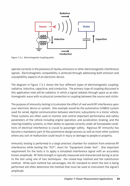
88Chapter 7: Power Measurement Applications
operate correctly in the presence of nearby emissions or other electromagnetic interference signals. Electromagnetic compatibility is achieved through addressing both emission and susceptibility aspects of an electronic device.
The diagram in Figure 7.3.1 shows the four different types of electromagnetic coupling: radiative, inductive, capacitive, and conductive. The primary type of coupling discussed in this application note will be radiative, in which a signal radiates through space as an elec-tromagnetic wave with no physical connection or coupling between the source and victim.
The purpose of immunity testing is to emulate the effect of real world RF interference upon your electronic device or system. One example would be the automotive CANBUS system used for wired, digital communication between electronic subsystems in a motor vehicle. These systems are often used to monitor and control important performance and safety parameters of the vehicle including engine operation, and acceleration, braking, and the steering/stability systems, so their ability to operate correctly under all foreseeable condi-tions of electrical interference is crucial to passenger safety. Rigorous RF immunity has become a mandatory part of the automotive design process as well as most other systems where any sort of malfunction could result in injury or damage to people or property.
Immunity testing is performed in a large anechoic chamber for isolation from external RF interference while testing the “EUT”, short for “Equipment Under Test”. One important requirement for the tests is to apply a simulated interference signal with an accurately known amplitude. RF field strength is typically measured and characterized during or prior to the test using one of two techniques: the closed-loop method and the substitution method. While each method has advantages, the IEC standard to which the test is being performed will often determine the method that must be used to instrument the signal’s amplitude.
Figure 7.3.1. Electromagnetic Coupling paths
IncreasingProbability
Increasing Crest Factor
Source Victim
Radiative
Inductive Capacitive
Conductive
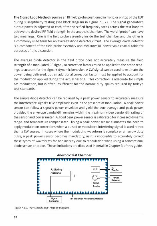
89
The Closed Loop Method requires an RF field probe positioned in front, or on top of the EUT during susceptibility testing (see block diagram in Figure 7.3.2). The signal generator’s output power is adjusted at each of the specified frequency steps across the test band to achieve the desired RF field strength in the anechoic chamber. The word “probe” can have two meanings. One is the field probe assembly inside the test chamber and the other is a commonly used term for an average diode detector circuit. The average diode detector is a component of the field probe assembly and measures RF power via a coaxial cable for purposes of this discussion.
The average diode detector in the field probe does not accurately measure the field strength of a modulated RF signal, so correction factors must be applied to the probe read-ings to account for the signal’s dynamic behavior. A CW signal can be used to estimate the power being delivered, but an additional correction factor must be applied to account for the modulation applied during the actual testing. This correction is adequate for simple AM modulation, but is often insufficient for the narrow duty spikes required by today’s test standards.
The simple diode detector can be replaced by a peak power sensor to accurately measure the interference signal’s true amplitude even in the presence of modulation. A peak power sensor can follow a signal’s power envelope and yield the true average and peak power, provided the envelope bandwidth remains within the maximum video bandwidth rating of the sensor and power meter. A good peak power sensor is calibrated for increased dynamic range, and temperature compensated. Using a peak power sensor eliminates the need to apply modulation corrections when a pulsed or modulated interfering signal is used rather than a CW source. In cases where the modulating waveform is complex or a narrow duty pulse, a peak power sensor becomes mandatory, as it is impossible to accurately correct these types of waveforms for nonlinearity due to modulation when using a conventional diode sensor or probe. These limitations are discussed in detail in Chapter 3 of this guide.
Radiating Antenna
Field Probe
PowerDetector
SignalGenerator
Anechoic Test Chamber
Closed Loop Method
EUTEUTTest Set
RF Radiation Absorbing Material
Figure 7.3.2. The “Closed Loop” Method Diagram

90Chapter 7: Power Measurement Applications
The Substitution Method uses an RF field probe to characterize and calibrate the RF field strength in the anechoic chamber before the EUT is placed inside (see block diagram in Fig-ure 7.3.3). The field strength is adjusted for each frequency step across the band and the EUT is positioned in the test environment. This method does not require field monitoring during the test and is referenced by some EMC test standards. While not required, a probe is often used during the test run just to monitor the RF field. This direct feedback assures good system performance.
Both the closed loop and substitution methods use a high power signal generator con-nected to a radiating antenna for repeatable RF signal transmission while testing the EUT. The closed loop method requires the field probe during testing, while the substitution method only states it can be used to improve measurement quality. In either case, it can be beneficial to use calibrated peak power sensor rather than the average diode detector in most field strength probes. This eliminates multiple calibrations, modulation correction factors, and the temperature compensation associated with the average diode detector, and provides both peak and average information about the interfering field’s characteris-tics. Without knowing these values, it is impossible to be certain that the EUT is operating in the intended interference environment.
Figure 7.3.3. The Substitution Method Diagram
Substitution Test Method
Radiating Antenna
Field Probe
PowerDetector
SignalGenerator
Anechoic Test Chamber
Radiating Antenna
SignalGenerator
Anechoic Test Chamber
EUTEUTTest Set
RF Radiation Absorbing Material
RF Radiation Absorbing Material
Substitution Test Method
Radiating Antenna
Field Probe
PowerDetector
SignalGenerator
Anechoic Test Chamber
Radiating Antenna
SignalGenerator
Anechoic Test Chamber
EUTEUTTest Set
RF Radiation Absorbing Material
RF Radiation Absorbing Material

91
Chapter 8: Performance Tips
A straightforward power measurement under “good” conditions is generally not a chal-lenge – simply hook up a power meter and read the results. However many application-related issues can make the process more challenging. This chapter discusses several topics on improving the performance of your power measurement:
• Reducingmeasurementnoise – a discussion of power measurement noise, and com-mon reduction techniques of simple filtering and synchronous averaging.
• OptimizingATEPerformance – a review of computer controlled testing, and how the entire system may be automated for increased throughput. Describes the common “sequential” ATE approach in which the controller steps through a sequence of steps many times to perform a multi-point measurement. Following this is a discussion of a modern alternative using preprogrammed source sweep control and buffered acquisi-tion in the power meter to significantly reduce test duration.
• AmplifierTestingStatisticalTechniques – explores a new approach for RF amplifier linearity testing using statistical analysis of a modulated power sweep rather than the traditional method of applying a series of CW tones to measure IP1 and IM3. The new method promises both increased test speed and enhanced compression characteriza-tion for estimating in-system performance of an amplifier.
8.1 Reducing Measurement Noise It is often necessary to perform power measurements across a wide dynamic range, and sensors may become challenged by signal power levels at both extremes. As discussed in Chapter 3, the top of the range usually has hard limits – both the average and peak power must remain within a safe (for the sensor) and calibrated range to be measured accurately. The lower end of the range, however, is more difficult to define.
All measurements must be made in the presence of noise – it is a part of every electrical measurement, including RF power. Unless the amplitude of the signal to be measured is considerably greater than the noise amplitude, that noise will add to the measured signal, and can result in considerable measurement uncertainty, as discussed in Chapter 9.
One convenient aspect of noise is that it is random. The finer details of noise are well un-derstood by Boonton Electronics’ sister brand, Noisecom, who specializes in components and instruments designed to generate or analyze various types of electrical noise. Because of this randomness, and its Gaussian distribution, it is possible to reduce the effect of noise while maintaining the characteristics of the signal one wishes to measure.

92Chapter 8: Performance Tips
As generated, power measurement noise is fairly wideband, and has a roughly “white” characteristic, in which the noise has constant power per Hertz. If the bandwidth is halved, so is the average noise power. When the noise bandwidth is greater than the bandwidth of the signal to be measured, it is possible to filter the noise bandwidth reducing the total amount of noise.
CW signals represent an extreme case. The bandwidth of a CW signal is effectively 0 Hz, so it is possible to filter the signal and noise together to sub-1 Hz bandwidth without af-fecting the accuracy of the measurement. Most power meters provide an averaging filter that averages a number of readings over a defined time interval to yield a filtered result. Increasing the averaging time setting will reduce the measurement noise at the expense of settling time to signal level changes.
Unfortunately, there are other types of noise present besides Gaussian noise, which cause increased filtering to reach a point of diminishing returns. A one-second filter time is gen-erally appropriate for -60 dBm with a CW diode sensor, but increasing the filter to ten seconds will not reduce noise by a factor of ten and permit the same accuracy at -70 dBm.
Most CW and average power meters include an “auto-filter” setting, in which the instru-ment chooses the filter time constant based on the measured power level. This can cause extended settling times when the power level is changed, so a good recommendation is that if you know your expected power level, set the filter manually for best performance.
1Hz 1KHz 10KHz 100kHz 1MHz 10MHz 100MHz
-50
-40
-30
-20
-10
0dbm
20200
+10Noise
Pow
er
WLAN Signal
(20 MHz)
GSM Signal
(200 KHz)
CW Signal
(1 Hz)
ƒHz
POWERdBm
20dB S/N
Ratio
Graph of average noise power versus noise bandwidth, showing how BW may be reduced to improve S/N

93
The averaging filter of most CW and average power meters, as well as peak power meters operating in continuous, free-run, or “modulated” mode is most often a sliding sample, or “window” filter, in which power readings are performed at a relatively fast rate, and then averaged together as needed. The filtered power reading at any given time is simply the average of the last “n” samples, where “n” is the filter time divided by the internal acquisition rate. Unweighted averages are the most common results, but other types of weightings are sometimes used to help accommodate fluctuating signals such as pulse waveforms. By continuously adding new samples and discarding old ones, the filter output can be recomputed and updated at the acquisition rate.
When measuring a wideband signal with a peak power meter, filtering out the noise can become more difficult. In peak power meters, it is often necessary to maintain measure-ment bandwidths of tens of MHz or more. Clearly, it is not possible to apply filters with mil-lisecond or second time constants without also filtering out desirable signal characteristics.
Take advantage of the redundancy of repetitive signals. Any periodic waveform can be synchronously filtered by averaging together multiple periods of the waveform. As long as the individual periods or waveform events can be made to align closely in time, it is pos-sible to average together even hundreds or thousands of individual cycles or sweeps, and produce a filtered waveform with significantly less visible noise and no degradation of the waveform’s amplitude and profile.
Effect of trace averaging for reducing noise on periodic pulse waveform. These screen shots both show one low-
level (-39dBm) pulse of a periodic waveform. The left trace has no averaging, and its min-to-max ratio is about 2.4
dB, representing the effective peak-to-peak measurement noise. Increasing averaging to 1024 in the right trace
reduces peak-to-peak noise during the pulse to less than 0.2dB, as well as bringing the noise floor down from about
-53dBm to below -70dBm.

94Chapter 8: Performance Tips
Synchronous waveform averaging is often called “trace averaging” or simply “averaging” in peak power meters operating in triggered or “pulse” mode. Sometimes the term “video averaging” is used, since it is familiar to spectrum analyzer users, but this can be confusing in power meters.
The source of this confusion is that some peak power meters offer an additional method for reducing noise – they are able to reduce the video bandwidth of the sensor or power meter input circuitry. This technique will not introduce errors as long as the video bandwidth of the measurement remains above the video bandwidth of the signal. In most cases, this bandwidth reduction offers only a modest reduction in noise, but it may make the differ-ence between a signal that can and can’t be measured, and it can be used in conjunction with filtering or averaging.
One other technique that can improve noise in peak power meters is simply to sample faster. If the power meter is already sampling at or above Nyquist rate, this method will not yield significant improvement. But if it is undersampling and has excess bandwidth, a faster sample rate will tend to filter the noise without impacting the signal.
8.2 Optimizing ATE Performance Like most of the instruments available today, modern Peak Power Meters usually include high-speed connectivity such as GPIB, LAN and/or USB interfaces to allow their operation to be controlled remotely by a PC or system controller, and therefore to be integrated into automated test equipment (ATE) systems. This functionality extends the instruments’ capabilities far beyond manual front panel operation since other devices can be combined with the power meter to provide a centralized location not only to control them but to col-lect and display data from multiple instruments as well. The intent here is to provide an overview of the additional functionality that can be obtained from an automated measure-ment application of power meters and an overview of some of the PC tools that facilitate instrument programming.
The ‘glue’ that ties instruments to a PC consists of a PC I/O interface such as the VISA I/O library. VISA is short for “VXIplug&play Systems Alliance”, and that group is now part of the IVI Foundation. With VISA, the physical interface used on the PC can be its built-in se-rial, Ethernet LAN or USB interface, a PCI-based GPIB interface card, a USB-to-GPIB interface cable or a combination of these I/O interfaces. The VISA library includes all the low-level drivers and functions required to use any of these interfaces for instrument control. This allows a portable, and bus-independent programming model which frees the developer from needing to implement a low-level communication channel for each instrument and bus in the system.

95
The last item the developer must select is a development environment to create the auto-mated software. The .NET IDE (integrated development environment) allows the choice of Visual Basic, C Sharp, or C++ for code development of automation software. There are also iconic programming environments such as Agilent VEE or National Instruments LabView, which allow users to create measurement automation applications without extensive pro-gramming experience. These, along with add-on libraries, utilities, and example programs can make it easier for the non-programmer engineer to develop automation software for his application.
Instrument-to-Host Communication. Most instruments today adhere to the SCPI (Stan-dard Commands for Programmable Instruments) software standard which defines a com-mon interface language for communication between instruments and computers. SCPI commands consist of ASCII text messages in a defined syntax and can be implemented in any PC host programming environment. The net result of conforming to this standard is that instruments with similar functions accept the same commands to execute those functions minimizing or eliminating software changes as instruments are replaced in test systems.
By definition all SCPI commands are sent as ASCII text strings, however measurement data returned by an instrument can be transferred either as ASCII text (default case) or in a binary format which is a more compact method of data transfer. The binary data transfer mode is configured by the host and is the most efficient manner of moving data when both the host and instrument use the IEEE floating point format for three reasons:
• ProcessingtimefortheBinary-to-ASCIIconversionontheinstrumentsideiseliminated
• ProcessingtimefortheASCII-to-binaryconversiononthehostsideiseliminated
• Thenumberofbytespervalueisreducedduetomoreefficientpackingandtheelimi-nation of delimiters
The default ASCII data transfer mode is the simplest to implement since all the formatting is performed transparently by the VISA library. It is also simplest for troubleshooting, since the bus transactions may be easily monitored and logged using readily available tools and utilities. But when reduced I/O traffic or data transfer speed become issues, the binary transfer mode can improve system efficiency with a little more effort at programming time.

96Chapter 8: Performance Tips
Measurement Automation. There are several compelling reasons to take the effort to automate the testing process:
• Itprovidesconsistencyofresultsbyeliminatingpossibleerrorsfromfrontpanelman-ual operation
• Timingofsystemeventsandmeasurementscanbemadetotallyconsistent
• Highermeasurement throughputprovideseither reduced test timeor theability tocollect more data in the same amount of time
• Automationfacilitateslargevolumeproductiontestingwheretesttimeandaccuracyare paramount
• CollectingresultsfrommultipledevicesforprocessinganddisplayonthePCallowsfornew ways of information display beyond the capability of each stand alone device
• Instrumentscanacquiredataatafasterratethantheirdisplayupdateratewhichcanbe bypassed via PC control to take advantage of this acquisition rate
• Itissimplertorecordandarchivemeasurementresultsforqualityassuranceorregula-tory purposes
Historically, RF power measurement in ATE systems has been performed via a query-re-sponse protocol. ASCII command and data transfer were used in both directions, either via the SCPI or proprietary protocols. However recent advances in power measurement, coupled with increased user requirements have now made it necessary to examine newer solutions for increased system throughput. Modern power meters, especially peak power meters, can have very high bandwidths and measurement rates, and their performance can far exceed the capability of a manual or query-response process to record and view the results.
In a typical ATE system with several instruments connected to the PC host, there is a pos-sibility that the overall speed and efficiency of the measurement process will degrade due to the amount of I/O traffic while communicating with the devices in the system. That is especially true when ATE systems attempt to mimic the manual testing method of ‘mea-sure then record’. That technique is still valid for most automated applications and will still be faster and more consistent when controlled by a PC, but it is only as fast permitted by the entire sequential measurement cycle. An automated, sequential measurement cycle typically contains the following steps for each measurement that must be performed:

97
One Loop of Sequencial Measurement Cycle
Step 1 Configure signal source Controller configures the signal source for next step in sweep: set power, frequency, attenuation, etc.
Step 2 Configure power meter Controller configures the power meter for any expected changes in the source sig-nal: set frequency, range, filtering, etc.
Step 3 Delay for signal settling Controller waits for a pre-programmed or adaptive time delay to allow the source to settle before starting measurement acquisition.
Step 4 Initiate new measurement Controller commands power meter to flush last reading and begin acquiring fresh measurement data.
Step 5 Acquire measurement data Power meter acquires measurement data and stops when complete. This step may or may not run concurrently with the next (data processing) step.
Step 6 Process measurement data Power meter processes the acquired data to yield a single measurement result. May run concurrently with previous step (measurement acquisition).
Step 7 Notification of “measurement ready” state Power meter notifies host that a new reading is ready via either a one-way notifica-tion or bidirectional polling process.
Step 8 Return measurement result Controller reads back the new measurement from instrument and saves the result.
Step 9 Next measurement in sequence Repeat steps 1 - 8 for each point to be measured.

98Chapter 8: Performance Tips
Step 7, “Signal measurement ready” may consist of either a polling activity, in which the host continuously polls the power meter to obtain the current measurement status, or via a notification process, such as a power-meter-to-host “interrupt”, which notifies the host when a measurement is ready. The IEEE-488 has a “Service ReQuest” (SRQ) signal line dedicated to this purpose, and many newer remote control protocols support or emulate this functionality. Once the host has received confirmation that a new result is ready, it can read and record the result as needed. The software design process of an ATE system needs to be aware and take advantage of this built-in functionality of current instruments to optimize their operation in a remotely controlled application.
In many systems, some steps of the measurement sequence can be combined to reduce the amount of bus traffic. For example, steps 4 through 8 are often replaced by a single query-response cycle, in which the power meter is told to “start a fresh measurement, stop when done, process, and return the result”. Once the command has been given, the controller simply waits for the power meter to return a finished result. The SCPI language allows for this sort of control via the READ query. This eliminates the need for a polling or interrupt-driven scheme for obtaining measurement status at the expense of tying up the remote control bus while the host is waiting for the power meter to respond.
The Modern Approach. Instruments today have enough intelligence built in to allow por-tions of this cycle to proceed without controller intervention. For example, a signal genera-tor can usually be programmed to perform a pre-configured power or frequency sweep with a single command. Likewise, a power meter may be commanded to acquire and buf-fer a series of readings, and return all of these values at once as a delimited list or binary data block. Sending a large number of values via a single bus transaction is considerably more efficient than sending them one at a time. In some cases, even the device under test may perform under “self control”, sometimes via a built-in test or diagnostic mode. One example of this is in cellular handset test, in which the handset be commanded to sequence through a programmed series of transmit power steps to test its power control subsystem.

99
Entire Buffered Sweep Measurement Cycle
Step 1 Configure and arm power meter Controller configures the power meter to acquire and buffer a sequence of mea-surements to match the expected sweep.
Step 2 Configure and initiate signal source sweep Controller configures the signal source to perform a full sweep: set start and end power, frequency, attenuation, sweep rate/duration, etc, then initiates the sweep (see Figure 8.2.1).
Step 3 Acquire sweep measurement data into power meter buffer Power meter acquires measurement data for entire sweep and stops when com-plete.
Step 4 Notification of “sweep ready” state Power meter notifies host that sweep is ready via either a one-way notification or bidirectional polling process.
Step 5 Return measurement sweep result Controller reads back all buffered readings from sweep and saves the result.
If suitable source control and measurement buffering is available, the entire measurement process can consist of a single sequence of host transactions to initiate the process, and final host step to read back all of the results. All other steps are managed and timed within the source and power meter, and can proceed without controller intervention. The chal-lenge of this approach is the difficulty in synchronizing the acquired measurement data with the sweep progress of the source signal. Without direct communication between the source and power meter, it can be difficult to determine what power step the source is on.Power Ramp
Time (0 to 10 seconds)
15
10
5
0
-5
-10
-15
dBm dBm
Figure 8.2.1. Power Ramp / Time-based power sweep

100Chapter 8: Performance Tips
The simplest method of synchronizing the two is to use time. The source is programmed to perform a linear sweep over a known time interval or at a known sweep rate, and the power meter is programmed to acquire data over exactly this same time interval. If both pro-cesses are begun in synchronization, and the source sweep rate and power meter recording rate are both accurately known, then it is not difficult to surmise the source sweep state based on the position of a reading in the array of returned measurements. This method works well with continuous and CW sweeps.
Another synchronization method is to use triggered acquisition, such as a hardware connec-tion between the signal source and power meter. Many signal generators have a synchro-nization output that is set to a logic state to indicate when each step in a pre-programmed sweep is occurring. Usually this signal is not asserted until the source is stable, which helps to address the need to program a signal settling delay. In this case, this synchronization pulse from the signal generator can then be used directly as a trigger command to the power meter, instructing it to record a reading each time it receives the pulse. Attention must be paid to timing and polarity – the source sweep must be programmed to occur at a rate appropriate for the power meter to complete a measurement at each desired point (see Figure 8.2.2).
Power Steps
Time (20 trigger events)
1510
50
-5-10-15-20-25
dBm
Figure 8.2.2. Power Sweep and power meter measurement of a single pulse within the sweep
101
Sometimes it may be helpful to control the source sweep externally. In this case, an ex-ternal pulse generator or custom hardware generates sync pulses which are sent to both the source and the power meter. Each time a pulse is received, the source will step and the power meter will acquire a new reading. The necessary time delays for settling and acquisi-tion can usually be programmed into the power meter, although it is also possible to use the pulse generator such a way as to step the source on the rising edge of the sync pulse, and acquire a fresh measurement on its falling edge.
Another option on peak power meters is to use the signal source itself for synchroniza-tion. When the signal to be measured is a periodic or pulsed waveform, the power meter’s internal trigger system may be used. The power meter is configured to initiate a sweep on the leading edge of each pulse. With suitable trigger delay settings to allow pre-trigger acquisition, the entire pulse can be acquired and processed, and its average power stored as a reading. Control of the source can provide both the “start sweep” synchronization, and the “acquire a new reading” signal (see Figure 8.2.3).
For instance, a GSM handset may be programmed to transmit a power sweep that tests each level of its internal power-control attenuator. The attenuator may have 128 levels, and the attenuation value is incremented for each GSM frame, with the handset transmit-ting for once timeslot in the frame. In GSM, a timeslot is 577 microseconds, and a frame of eight timeslots is 4.615 milliseconds, so the phone will transmit a pulsed signal with a 217 Hz period.
The power meter is instructed to trigger on the signal’s rising edge for each timeslot, and perform and record an interval average power measurement over the active portion of the timeslot (typically the middle 550 microseconds of the pulse). A trigger holdoff setting of about 4.5 ms should be used to ensure the power meter does not retrigger before the next timeslot begins, and the trigger level will need to be set low enough that even the lowest pulse amplitude will trigger a sweep.
To initiate the sweep, the power meter is configured and armed, and the source command-ed to begin a sweep of 128 frames. This sweep will take 128 Frames / 217 Hz = 590 milliseconds to complete, and at the end of the sweep, the controller simply queries the power meter to retrieve the measurement buffer containing all 128 readings. If carefully optimized, the entire process should take less than one second.
All this is possible due to the inclusion of fast “buffered measurement modes” in modern power meters. In these modes, the instrument acquires a series of measurements into its memory buffer with little or no processing. If needed, the data may be post-processed after the acquisition cycle is completed. This buffered acquisition mode is setup and ex-ecuted under PC control. These results can be collected in a free run mode or by a trigger

102Chapter 8: Performance Tips
event. Data rates in the range up to 1000 readings per second are typical for the free run mode, but the triggered mode rate may be less due to the latency time to re-arm for the next trigger event. Buffer sizes of 1 million readings or more per channel are typical. For buffers that are implemented as FIFO’s (First In First Out), this data collection technique can continue beyond the time it takes to fill the buffer since FIFO’s can be read out and sent to the host while still being filled. For example, reading the buffer when it is half filled in most cases allows continuous measurement acquisition as read and write pointers are updated as the FIFO is accessed. This is true as long as the time to read a fraction of the buffer (which frees that area of the buffer) is less than the time to fill the entire buffer. If necessary, binary data transfer can be used to reduce data transfer times.
For the CW (continuous wave) mode up to 1 million readings (typical) can be stored at pre-programmed rates as high as 1000 readings per second for a specified number of read-ings (and therefore a known time duration). The data can then be transferred to the host PC after all the readings have been stored in the buffer. This allows the user to trade off between time resolution, measurement duration, and data set size. This mode is best for continuous modulation formats where the power is stepped at periodic time intervals. In this mode the power meter is free-running and readings are stored in the buffer at specific time intervals.
For the power ramp case, the test condition is to linearly increase the power from -10 dBm to +10 dBm over a ten second duration with a measurement rate of 20 readings per second for a total of 200 readings which get stored every 0.5 seconds. The results are read by the host PC every time 20 readings are stored in the buffer. The acquisition stops after the 200 readings have been collected. The read rate of the buffered results by the PC is much faster
Figure 8.2.3. Command sequence to set up and read the measurement buffer over the entire power sweep of 128
pulse levels
103
than the rate the readings are stored in the buffer which means that this mode could be used for long term monitoring of the power sweep over multiple power sweep cycles with either a wait time to reset the power level or directly sweep up and down continuously. In other words, the number of readings to acquire can be as large as the maximum size of the buffer and the power meter will continuously update the read and write locations of the buffer during the measurement process.
For the pulsed signal types, triggered pulse measurements can also be buffered to record power sweeps for discontinuous formats such as GSM or TDMA. Each pulse trigger stores a reading in the buffer which is usually the average power between two on screen cursors. Modern power meters have powerful triggering features that allow synchronization with most types of pulse and burst modulation formats including an external trigger event. Buffered measurements in the pulse mode can also be used with a continuous power sweep for the case where a trigger event is used to indicate when the power change has properly settled in the device under test. Another case where a continuous power sweep can be used is for devices that accept continuous power as an input and provides pulsed output power. For these cases absolute timing of the synchronization pulses is not critical – they only need to be repeatable. GSM timing generally has pulse repetition periods longer than 3 milliseconds should not present a problem, but signals with pulse periods less than about 3 to 4 milliseconds may skip pulses due to the trigger re-arm time which can range from 1 to 15 milliseconds or more, depending upon timebase and trigger settings.
For the above cases the data can be graphed either as output power vs. input power or power vs. time where time is obtained from the reading rate or the trigger rate. If the trig-ger is an external event then the horizontal axis of the graph can represent any parameter step change that the trigger represents such as temperature steps or distance increments.
Another application well suited for an ATE system is testing of high gain amplifiers par-ticularly pulsed output amplifiers. A typical ATE system for this application would consist of a two channel peak power meter, a signal generator (or sweeper) and possibly a pulse generator to acquire and display pulsed input power, output power and gain for a given fre-quency range. In this configuration, the PC controls the frequency and power level from the signal generator and collects power readings to display power or gain vs. frequency. The frequency axis is constructed either by trigger events that step the frequency output of the sweeper or by measuring a frequency to voltage output of the sweeper at each power reading during the frequency sweep. This ATE configuration is very close to the function-ality of a scalar analyzer. If the trigger event that yields the frequency can be associated with other events such as time, angular or linear position, temperature, or other then the measured power can be graphed or correlated to that event.

104Chapter 8: Performance Tips
As an example of high speed power meter data acquisition Figure 8.2.4 represents a 200 point timed power sweep from -10 dBm to +10 dBm for an amplifier showing a nominal gain of 15 dB and going into compression above +12 dBm.
8.3 Communication Amplifier Testing Digital communication amplifiers for LTE and WiMAX signals require a broad frequency band and wide dynamic range to accommodate complex modulation schemes. Traditional figures of merit like the 1 dB compression point and the third order intercept for testing lin-earity will not be sufficient to account for peak-to-average ratios in excess of 15 dB. Peak power meters like Boonton’s 4500 series provide amplifier communication designers with an alternative method for testing amplifier linearity. This section will explain the value of statistics for measuring the peak to average ratio of these complex digital signals.
The 1 dB compression point of an amplifier is defined as the output power at which the de-vice’s gain drops by 1 dB from its small-signal value. This is typically known as P1dB or CP1. To measure the compression point, a single CW tone (carrier) from an RF signal generator is supplied to the input of the amplifier, and ratio of the output to input power is measured to yield the amplifier’s small-signal gain. The input amplitude is then gradually increased until that measured ratio decreases by 1 dB, representing 1 dB gain compression. This figure is commonly used as a reference point for the beginning of amplifier non-linearity, and is approximately equal to the maximum useable peak output power for the amplifier.
Figure 8.3.1 illustrates two historical methods for evaluating amplifier linearity with a CW input signal. The 1 dB compression point and the third-order intercept are two figures of merit that provide designers with assumptions about amplifier performance. In the past, using a CW signal to measure the behavior of a narrow band amplifier was common, but for modern broad band devices this is an unnecessary limitation.
20
18
16
14
12
10
8
6
4
2
0
-10 -5 0 5 10
Input Power (dBm)
Out
put P
ower
(dBm
)
Figure8.2.4. Typical Amplifier Gain sweep

105
Multiple tones can be substituted for the CW test signal, or a modulated or noise signal with frequency components across the amplifier’s entire operating band can be used. For communication amplifiers that typically amplify signals with a large peak-to-average pow-er ratio (crest factor), the average input power must be reduced sufficiently so that the expected peaks rarely or never saturate the device. Depending upon the amplifier’s target application, designers typically estimate an amplifier’s maximum average output power will be 6 to 12dB lower than its 1dB compression point. This estimate will allow digital signals with a high crest factor to saturate the amplifier only occasionally to maintain an acceptable BER.
The 3rd order intercept point is an additional figure of merit using the third order har-monic product of two mixed tones. This is commonly referred to as IP3, short for the third order intercept. The third order harmonic product of two mixed tones is referred to as IM3, or the third order inter-modulation product. This is the beginning of a line having a 3:1 slope that intersects with the 1:1 slope of input vs. output power at IP3, or the third order intercept point. These values are shown in Figure 8.3.1.
The 1 dB compression point and IP3 are two figures of merit used to estimate the spurious free dynamic range (SFDR) of the amplifier. The SFDR is calculated by selecting a point 1/3 the Y-axis distance below the third order intercept value with respect to the thermal noise limit of a 50 ohm resistor, which is -174 dBm/Hz. The signal’s useful dynamic range, or UDR is equal to the SFDR minus the measurable noise floor of the amplifier (NF). The UDR is calculated by selecting a point 1/3 the distance in dB from P3 to the amplifier noise floor assuring that IM3 products will be below that noise floor. The noise floor can be estimated or measured using noise figure. These assumptions may artificially limit system dynamic range (see Figure 8.3.2).
Input Pwr
OutputPwr
Single Tone
Input Pwr
OutputPwr
Two Tones
1dBCP IM3
3dB/dB
1dB/dB
1P3
1dB comp pt.
Figure 8.3.1. The 1 dB compression point and third-order intercept figures of merit

106Chapter 8: Performance Tips
Amplifier compression test system. A simple test to measure the 1 dB compression point is shown in Figure 8.3.3 below, and requires the following equipment: a CW Signal source, dual-channel power meter, two suitable power sensors, a directional coupler, test amplifier, power supply, and all the necessary cable connections. For higher power systems, some form of additional signal attenuation may be required to maintain signal levels within the range that can be measured by the power sensors.
IP3
PowerOut
NF
UD
R
SFDR
Power In
1/3
2/31dB
3dB
10dB
PIM3
P3
thir
d ha
rmon
ic
P1dB
Thermal Noise
Figure 8.3.2. IP3 and IM3 figure of merit, and SFDR of an amplifer
Signal Source
Power Meter
ReferenceSensor
MeasurementSensor
BiasSupply
Coupler
TP1 TP2
DUT
14.7 dBm
15Y
Figure 8.3.3. Amplifier Compression Test System Block Diagram

107
Part 1: Measure the 1 dB compression point of the DUT
The 1 dB compression point of an amplifier can also be measured using a peak power meter in average mode as illustrated in Figure 8.3.4. Measure the input, and output of the ampli-fier simultaneously at low-to-medium output power, and compute the small-signal gain. The left screen shot shows the input power on Channel 1, and output power on Channel 2. The gain is the ratio of Channel 2 to Channel 1, and is shown in the lower right of the bot-tom window. At this operating level (2 dBm output power), the measured gain is 20.026 dB.
The right side of figure 8.3.4 showsthe input power has been increased until the auto-matically computed gain value in the lower window has fallen by 1 dB from its small-signal value on the left side. The output power at this point is measured to be 15 dBm, which would be the P1dB figure-of-merit for this amplifier.
Using statistics to measure the peak to average ratio. Unlike simple, average power measurements using CW tones, statistical analysis can be used to compare the peak to average ratio of the signal in percent with respect to the total signal time. The peak power values are sorted, or binned according to their magnitude. They can be divided by the aver-age power and displayed in log-log plot in dBr as crest factor. A common communications display is the CCDF, or complementary cumulative distribution function. The CCDF in Figure 8.3.5 shows how long a particular crest factor is being transmitted as a percentage of total signal time. 0 dBr is equal to the average power and 0% time is equal to maximum crest factor. In this example, a crest factor probability of 0.0001% occurs at 15 dBr with respect to the average.
Figure 8.3.4. Two-Channel measurements showing amplifier gain (Channel 2 to Channel 1 ratio) dropping by 1dB

108Chapter 8: Performance Tips
Demonstration signal. The time-domain screen capture shown Figure 8.3.6, below is a noise-like wireless digital communication signal that is difficult to measure using a spec-trum analyzer or oscilloscope. The power meter is an effective tool for measuring the crest factor of these signals using statistical analysis, however a time-domain display does not provide much information about peak power events that occur very infrequently. Statisti-cal analysis is a much more useful technique which makes it possible to characterize the probability of occurrence of rare peak (high crest factor) events. Since amplifiers and other devices are most stressed by these peaks, that is where signal compression or clipping will be most likely to result in a loss of data. A meaningful statistical measurement requires a large number of samples and Boonton power meters can collect millions of peak power measurements in seconds.
Figure 8.3.5 CCDF of a modulated communication signal
Frequent Events
IncreasingProbability
Infrequent Events
Increasing Crest Factor
Figure 8.3.6. A noise-like CDMA communication signal displayed in the time domain

109
Using CCDF distributions to compare amplifier input and output. The screen shot in Fig-ure 8.3.7 contains two CCDF distributions. The transmitter signal in blue is the reference, or input channel and the yellow signal is the output of the DUT. This allows direct compari-son of input vs output using the normalized CCDF of the peak to average ratios. This view allows comparison of the signal over the entire dynamic range of the amplifier using the particular modulation format and frequencies of interest.
The graph button on a Boonton 4540 allows the user to toggle between the 1 dB compres-sion point, and the dual CCDF display. The difference between a narrow band figure of merit and the statistical display is illustrated by the peak to average ratio deviation, well before the 1 dB compression point is reached. The crest factor is not measured using the 1 dB, or 3rd order intercept point figures of merit. This is clearly shown in Figure 8.3.8.
The statistical methods used in this discussion can infer BER qualities before the entire receiver circuit has been assembled. This can save valuable design, and compliance testing time.
Figure 8.3.7. Dual CCDF of typical CDMA signal
Frequent Events
IncreasingProbability
Infrequent Events
Increasing Crest Factor
Figure 8.3.8. Difference between conventional (peak and average) and CCDF statistical analysis
Toggle betweenscreens using the
graph button

110Chapter 9: Measurement Accuracy
Chapter 9: Measurement Accuracy
RF power meters have long been accepted as accurate measurement standards, but just how accurate are the power measurements they yield? Calculating the accuracy of aver-age and peak RF power measurements requires more than just a glance at a specification sheet. While many users ask “how accurate is the meter,” the metrologist more properly asks “what is the uncertainty of this particular measurement?” Uncertainty is a quantifi-able measurement of exactly where measurement errors are, or more importantly, may be present.
This chapter will examine the various sources of measurement uncertainty, describe how these uncertainties are combined to yield a single uncertainty value, and show two sample uncertainty calculations for typical power measurement scenarios.
9.1 Introduction to Uncertainty RF power measurement accuracy depends on a variety of factors derived from the measur-ing instrument, device under test (often abbreviated “DUT”), characteristics of the signal being measured, instrument settings, and environmental factors. Calibration, signal fre-quency, level and modulation, source and load mismatch, and noise all play an important role in the determining total uncertainty.
Each of these factors adds its own contribution to the uncertainty – some large and some negligible. These “uncertainty terms” can be combined mathematically to yield a single uncertainty value for a particular power measurement. However, many of the values can vary considerably from one measurement application to the next, even with identical equipment, so there is never a single “data sheet value” for power measurement accuracy.
Uncertainty Values. When combining uncertainty values, it is important that all numbers be in the same units. Uncertainty is typically given as a fraction or percentage, with 0.0% indicating that term does not contribute any error to the reading. Sometimes, uncertainty values are provided as a logarithmic value, often in the form of “± x.xx dB”. The following formulas may be used to convert between percent uncertainty and dB tolerance:
U% = (10(UdB
/10) -1) × 100 and UdB = 10 × Log10(1 + (U% / 100))
Worst Case Uncertainty. Uncertainty values for each term are usually specified as “worst-case” values – that is the measurement uncertainty due to that particular item will never be greater than the specification. In some cases, “typical” values are also given, and can be used to better understand the characteristic of that term.

111
The “combined worst-case uncertainty” approach is a very conservative method for calcu-lating accuracy where the worst-case values of each individual uncertainty term are added together. The formula for worst-case measurement uncertainty is:
UWorstCase = U1 + U2 + U3 + U4 + ... UN
But typically most of the uncertainty terms are independent of one another, so the prob-ability of them all existing at worst-case conditions simultaneously is extremely small. For this reason, a more realistic approach known as the “root-sum-of-squares” (RSS) tech-nique is generally used to combine the terms to yield a single, expected uncertainty val-ue. To compute combined uncertainty with the RSS technique, each uncertainty term is squared, the squares are added together, and the square root of the resulting summation is calculated.
URSS = √ ( U12 + U2
2 + U32 + U4
2 + ... UN2 )
Uncertainty Distributions. A problem with the basic RSS method is that it does not ac-count for the fact that the distribution of errors for each term may have different shapes within the worst-case uncertainty bounds. Certain types of errors will vary with a normal, or Gaussian distribution, with most existing within a narrow range, and fewer errors for larger error values. The worst-case limits will typically be set several standard-deviations away, and often some method of guaranteeing conformance will exist. Other errors may vary linearly within a set of bounds, yielding a rectangular distribution, with equal prob-ability of any error within the limit bounds, large or small. Other distribution shapes such as “U-shaped” are possible as well – often resulting from normal distributions that are “cut off” or forced within a range by some adjustment process.
To account for these varying probabilities of these error distributions, the worst-case un-certainty values for each term may be scaled, or normalized by an appropriate constant to adjust for that term’s probability distribution or shape. Once the worst-case values are normalized in this way, the RSS process can yield more meaningful result.
The distribution shape is a statistical description of how the actual error values are likely to vary from the ideal value. Three main types of distributions are normal (Gaussian), rectan-gular, and U-shaped. The “K” multipliers for each type of distribution are:
Distribution Multiplier K
Normal √ (1/4) = 0.500
Rectangular √ (1/3) = 0.577
U-shaped √ (1/2) = 0.707
112Chapter 9: Measurement Accuracy
The formula for calculating RSS measurement uncertainty from worst-case values and dis-tribution shape scale factors is:
URSS = √ [ (U1K1)2 + (U2K2)2 + (U3K3)2 + (U4K4)2 + ... (UNKN)2 ]
where U1 through UN represent each of the worst-case uncertainty terms, and K1 through KN represent the normalizing multipliers for each term based on its distribution shape.
This calculation yields what is commonly referred to as the combined standard uncertainty, or UC, with a level of confidence of approximately 68 %. To gain higher levels of confidence the Expanded Uncertainty is often employed. Using a statistical coverage factor of two will provide an expanded uncertainty with a confidence level of approximately 95%:
UEXPANDED = 2 × UC
This is generally accepted method within the RF power measurement industry.
9.2 Power Measurement Uncertainty Contributions As outlined above, there are a number of factors that contribute to uncertainty in RF peak power measurements. This section will define the major factors. It should be noted that there is no standard set of defined uncertainty terms, and different instrument manufac-turers may group or name the terms differently. The following list describes the terms that are used for computing uncertainty for power measurements performed with Boonton Peak and CW power meters and sensors.
Instrument Uncertainty. This term represents the amplification and digitization uncer-tainty in the power meter, as well as internal component temperature drift. Cable and connector loss between the sensor and power meter may also be included. In most cases, this is very small, since absolute errors in the circuitry are calibrated out by field calibration processes such as sensor zero and fixed calibration, or sensor step calibration (“AutoCal”), leaving only relative linearity errors. Instrument Uncertainty is typically a datasheet value.
Calibrator Level Uncertainty. This term is the uncertainty in the calibrator’s output level for a given setting for calibrators that are maintained in calibrated condition. The value of is term is typically a single datasheet value for fixed-output (0 dBm) power references, and will vary with level for variable-output calibrators.
The value to use for calibration level uncertainty depends upon the sensor calibration tech-nique used. If AutoCal was performed, the calibrator’s uncertainty at the measurement power level should be used. For sensors calibrated with the “FixedCal” method, the calibra-tor is only used as a single-level source, and you should use the calibrator’s uncertainty

113
value at the FixedCal level, 0 dBm for most sensors. This may make FixedCal seem more accurate than AutoCal at some levels, but this is usually more than offset by the reduction in shaping error afforded by the AutoCal technique.
For sensors that are not field calibrated, the calibrator uncertainty term may be neglected.
Calibrator Mismatch Uncertainty. This term is the mismatch error caused by impedance differences between the calibrator output and the sensor’s termination. It is calculated from the reflection coefficients of the calibrator (rCAL) and sensor (rSNSR) at the calibration frequency with the following equation:
Calibrator Mismatch Uncertainty = ±2 × rCAL × rSNSR × 100 %
The calibrator reflection coefficient is typically a specification for the calibrator or RF power reference output, and may be provided as a VSWR. If so, the corresponding reflection coef-ficient may be looked up in the reference table in Section 10.2 of this guide, or computed with the following formula:
Reflection Coefficient (rCAL) = (VSWR -1) / (VSWR +1)
The sensor reflection coefficient, rSNSR is frequency dependent, and is usually provided as a sensor datasheet value. If it is listed as a VSWR value, the equation above may be used to convert.
Source Mismatch Uncertainty. This term is the mismatch error caused by impedance dif-ferences between the measurement source’s output and the sensor’s termination. For many measurements, this is the single largest error term, and care should be used to ensure the best possible match between source and sensor. Both the sensor and DUT contribute to this term, as does the mating of the two connectors. The source mismatch uncertainty value is calculated from the reflection coefficients of the source (rSRCE) and sensor (rSNSR) at the measurement frequency with the following equation:
Source Mismatch Uncertainty = ±2 × rSRCE × rSNSR × 100 %
The source reflection coefficient is a characteristic of the RF source under test, and will usu-ally vary with frequency, and sometimes level. It must be supplied, measured or estimated.
The sensor reflection coefficient, rSNSR is frequency dependent, and is usually provided as a sensor datasheet value.
114Chapter 9: Measurement Accuracy
Both the source and sensor reflection coefficients may be computed from their correspond-ing VSWR values using the formula above if required.
Sensor Shaping Error. This term is sometimes called “linearity error” and is the residual non-linearity in the measurement after the sensor’s output has been linearized and scaled to a power value by the calibration and shaping processes.
Calibration is typically performed at discrete level steps and is extended to all levels via a curve-fitting technique. The sensor shaping error is close to zero at these calibration points, and increases in between due to imperfections in the curve-fitting algorithm.
An additionally component of sensor shaping error is due to the fact that the sensor’s transfer function may not be identical at all frequencies. The published shaping error in-cludes terms to account for these deviations.
If your measurement frequency is close to your field calibration frequency and you are measuring at a level close to one of the field linearity calibration points, it is probably ac-ceptable to use a value lower than the published uncertainty in your calculations.
Sensor Temperature Coefficient. This term is the error that occurs when the sensor’s tem-perature has changed significantly from the temperature at which the sensor calibration was performed. It is usually specified in dB/degree C or similar units, and may be a single value or level dependent. In this case, the term’s value must be computed based on the dif-ference between the current measurement temperature and the calibration temperature, and then scaled to a percent uncertainty.
Note that when the measurement is performed at the exact same temperature as field calibration, this term will cancel to zero.
Sensor Noise. This term is the uncertainty contribution by the intrinsic noise that is a part of all power measurements. It is not necessarily generated within the sensor itself, but rather is noise from the entire measurement chain. For convenience, however, the measurement noise is usually specified as input referred noise, and is the amount of power (usually in dBm or nanowatts) which appears to be present at the sensor input.
Sensor noise is an apparent power quantity, and may be reduced by filtering or averaging as discussed in Section 8.1 of this guide. The noise usually approximates bandlimited white Gaussian noise, and therefore its amplitude (and uncertainty contribution) may be reduced by narrowing the measurement bandwidth.

115
Sensor datasheets often give the effective noise at a certain level of filtering. For con-tinuous-mode measurements, the degree of filtering may be specified as an integration time or reading averaging factor. For Pulse-mode measurements, a video averaging figure is often used. Regardless of the method, it is important to understand the relationships between the acquisition mode, sample rate, and filtering to ensure that the correct noise power value is used.
The uncertainty due to sensor noise depends upon the ratio of the noise to the signal power being measured:
Noise Uncertainty = ± Sensor Noise (in watts) / Signal Power (in watts) × 100 %
The noise rating of a particular power sensor may be found on the sensor datasheet. It may be necessary to adjust the sensor noise for more or less filtering or averaging, depending upon the application. As a general rule (within a decade of the datasheet point), noise is in-versely proportional to the filter time or averaging used. Noise error is usually insignificant when measuring at high levels (25 dB or more above the sensor’s minimum power rating).
Sensor Zero Drift. This term is the reading uncertainty due to long-term change in the zero-power reading that is not a random, noise component. Increasing filter or averaging will not reduce zero drift. For low-level measurements, this can be controlled by zeroing the meter just before performing the measurement.
The uncertainty due to zero drift depends upon the ratio of the drift to the signal power being measured:
Zero Drift Uncertainty = ± Sensor Zero Drift (in watts) / Signal Power (in watts) × 100 %
Likesensornoise,Zerodrifterrorisusuallyinsignificantwhenmeasuringat25dBormoreabove the sensor’s minimum power rating. The drift specification sometimes indicates a timeintervalsuchasonehour.IfthetimesinceperformingasensorZeroorAutoCalisveryshort, the zero drift is greatly reduced.
Sensor Frequency Calibration Factors. Sensor frequency calibration factors, or “calfac-tors” are used to correct for sensor frequency response deviations. These calfactors are characterized during factory calibration of each sensor by measuring its output at a series of test frequencies spanning its full operating range, and storing the ratio of the actual applied power to the measured power at each frequency. During measurement operation, the power reading is multiplied by the calfactor for the current measurement frequency to correct the reading for a flat response.

116Chapter 9: Measurement Accuracy
Calfactors are also called “efficiency factors,” and can be provided as either a percent or a dB correction value. They are usually factory generated, but like any calibration, include a number of uncertainties. These uncertainties occur due to both standards uncertainty, and measurement uncertainty in the calibration process, and will be different for each fre-quency calibrated. Both worst case and RSS uncertainties are provided for the frequency range covered by each sensor, and are listed on the sensor datasheet and in the Boonton Electronics Power Sensor Manual.
If the measurement frequency is between sensor calfactor entries, the most conservative approach is to use the higher of the two corresponding uncertainty figures. It is also be possible to estimate the figure by linear interpolation.
If the measurement frequency is identical to the field calibration frequency, a calfactor uncertainty value of zero may be used, since any absolute error in the calfactor cancels out during field calibration. At frequencies that are close to the calibration frequency, the calfactor uncertainty is only partially cancelled out during calibration, so it is generally ac-ceptable to take the uncertainty for the next closest frequency, and scale it down.
9.3 Sample Uncertainty Calculations The following examples shows calculations for two measurement scenarios using the Boon-ton Model 4540 RF Power Meter. The first is a CW example using the 51075 CW sensor, a general-purpose, 18 GHz CW Dual-Diode power sensor. The second example shows the same instrument performing a measurement with a 57518 power sensor, a typical choice for mid-bandwidth modulated signals such as CDMA. Additional information on these Boonton products may be found in Chapter 11 of this guide.
The figures used in these examples are meant to show the general technique, and do not apply to every application. Some common sense assumptions have been made to illustrate the fact that uncertainty calculation is not an exact science, and requires some understand-ing of your specific measurement conditions. These are in spirit with the RSS method, which is itself a method for estimation.
Typical Example #1: Boonton 4540 RF Power Meter with 51075 CW Power Sensor
Measurement Conditions
Source Frequency 10.3 GHz
Source Power -55 dBm (3.16 nW)
Source VSWR 1.50 (reflection coefficient = 0.20) at 10.3 GHz
AutoCal Source Internal 50 MHz Calibrator
AutoCal Temperature 25°C
Current Temperature 25°C

117
In this example, assume that an AutoCal was performed on the sensor immediately before the measurement. This will reduce certain uncertainty terms, as discussed below.
Step 1: The Instrument Uncertainty figure for the 4540 Series is ± 0.20 %. Since a portion of this figure includes temperature drift, the instrument uncertainty is ± 0.10 %, or half the published figure.
UInstrument = ± 0.10%
Step 2: The Calibrator Level Uncertainty for the power meter’s internal, 50 MHz calibrator may be read from the calibrator’s specification. It is ± 0.105 dB, or ± 2.45 % at a level of -55 dBm.
UCal Level = ± 2.45%
Step 3: The Calibrator Mismatch Uncertainty is calculated using the formula in the previous section, using the internal 50 MHz calibrator’s published figure for rCAL and calculating the value rSNSR from the VSWR specification on the 51075 sensor datasheet.
rCAL = 0.024 (internal calibrator’s reflection coefficient at 50 MHz)
rSNSR = (1.15 - 1) / (1.15 + 1) = 0.070 (calculate reflection coefficient of 51075, max VSWR = 1.15 at 50 MHz)
UCalMismatch = ± 2 × rCAL × rSNSR × 100 % = ± 2 × 0.024 × 0.070 × 100 % = ± 0.34%
Step 4: The Source Mismatch Uncertainty is calculated using the formula in the previous section, using the DUT’s specification for rSRCE and calculating the value rSNSR from the VSWR specification on the 51075 sensor datasheet.
rSRCE = 0.2 (DUT source reflection coefficient at 10.3 GHz)
rSNSR = (1.40 - 1) / (1.40 + 1) = 0.167 (calculate reflection coefficient of 51075, max VSWR = 1.40 at 10.3 GHz)
USourceMismatch = ± 2 × rSRCE × rSNSR × 100 % = ± 2 × 0.20 × 0.167 × 100 % = ± 6.68%

118Chapter 9: Measurement Accuracy
Step 5: The uncertainty caused by Sensor Shaping Error for a 51075 CW sensor that has been calibrated using the AutoCal method can be assumed to be 1.0%, as per the discus-sion in the previous section.
UShapingError = ± 1.0%
Step 6: The Sensor Temperature Drift Error depends on how far the temperature has drifted from the sensor calibration temperature, and the temperature coefficient of the sensor. In this example, an AutoCal has just been performed on the sensor, and the temperature has not drifted at all, so we can assume a value of zero for sensor temperature drift uncertainty.
USnsrTempDrift = ± 0.0%
Step 7: This is a relatively low-level measurement, so the noise contribution of the sensor must be included in the uncertainty calculations. We’ll assume default filtering. The signal level is -55 dBm, or 3.16 nW. The RMS noise specification for the 51075 sensor is 30 pW, from the sensor’s datasheet. Noise uncertainty is the ratio of these two figures expressed as a percentage.
UNoise Error = ± Sensor Noise (in watts) / Signal Power (in watts) = ± (30.0e -12 / 3.16e -9) × 100 % = ± 0.95%
Step 8:TheSensorZeroDriftcalculationisverysimilartothenoisecalculation.Forsensorzero drift, the datasheet specification for the 51075 sensor is 100 pW, so we’ll take the liberty of cutting this in half to 50 pW, since we just performed an AutoCal, and it’s likely that the sensor hasn’t drifted much.
UZero Drift = ± Sensor Zero Drift (in watts) / Signal Power (in watts) = ± (50.0e -12 / 3.16e -9) × 100 % = ± 1.58%
Step 9: The Sensor Calfactor Uncertainty is calculated from the uncertainty values in the Boonton Electronics Power Sensor Manual. There is no entry for 10.3 GHz, so we’ll have to look at the two closest entries. At 10 GHz, the calfactor uncertainty is 4.0 %, and at 11 GHz it is 4.3 %. These two values are fairly close, so we’ll perform a linear interpolation to estimate the uncertainty at 10.3 GHz:
UCalFactor = [ ( F - F1 ) × (( CF2 - CF1 ) / ( F2 - F1 )) ] + CF1 = [ ( 10.3 - 10.0 ) × (( 4.3 - 4.0 ) / ( 11.0 - 10.0 )) ] + 4.0 = 4.09%

119
Step 10: Now that each of the individual uncertainty terms has been determined, we can combine them to calculate the worst-case and RSS uncertainty values: U (± %), (U×K)2 ( %2 )
In this example, the two largest contributions to total uncertainty are the source mismatch and the sensor CalFactor. Also note that the expanded uncertainty is approximately one-half the value of the worst-case uncertainty. This is not surprising, since the majority of the uncertainty comes from just two sources. If the measurement frequency was lower, these two terms would be reduced, and the expanded uncertainty would probably be less than half the worst-case. Conversely, if one term dominated (for example if a very low level measurement was being performed, and the noise uncertainty was 30%), the expanded uncertainty value would be expected to approach the worst-case value. The expanded uncertainty is 0.45 dB.
Uncertainty Term UWorstCase
(± %)
“K”
Distribution Multiplier
(U×K)2
( %2 )
RSS
1. instrument 0.10 0.500 0.0025
2. calibrator level 2.45 0.577 1.9984
3. calibrator mismatch 0.34 0.707 0.0578
4. source mismatch 6.68 0.707 22.305
5. sensor shaping error 1.00 0.577 0.3333
6. sensor temperature drift 0.00 0.577 0.0000
7. sensor noise 0.95 0.500 0.2256
8. sensor zero drift 1.58 0.577 0.8311
9. sensor calibration factor 4.09 0.500 4.1820
Total Worst Case Uncertainty ± 17.19 %
Total sum of squares 29.936 %2
Combined Standard
RSS Uncertainty UC
±5.47%
Expanded RSS Uncertainty
U (coverage factor k = 2)
±10.94%
(±0.45 dB)

120Chapter 9: Measurement Accuracy
Typical Example #2: Boonton 4540 RF Power Meter with 57518 Peak Power Sensor
In this example, we will assume that an AutoCal was performed on the sensor earlier in the day, so time and temperature drift may play a role in the uncertainty.
Step 1: The Instrument Uncertainty figure for the 4540 Series is ± 0.20 %. Since it has been a while since AutoCal, we’ll use the published figure.
UInstrument = ± 0.20%
Step 2: The Calibrator Level Uncertainty for the Model 2530 External 1 GHz calibrator may be calculated from the calibrator’s specification. The 0 dBm uncertainty is 0.065 dB, or 1.51 %. To this figure, we must add 0.03 dB or 0.69 % per 5 dB step from 0 dBm. 13 dBm is 2.6 5 dB steps (13/5) away from 0 dBm. Any fraction must always be rounded to the next highest whole number, so we’re 3 steps away.
UCalLevel = ± (1.51 % + (3 × 0.69 %)) = ± 3.11%
Step 3: The Calibrator Mismatch Uncertainty is calculated using the formula in the previous section, using the 1 GHz calibrator’s published figure for rCAL and calculating the value rSNSR from the VSWR specification on the 57518 sensor datasheet.
rCAL = 0.091 (internal 1 GHz calibrator’s reflection coefficient)
rSNSR = (1.15 - 1) / (1.15 + 1) = 0.070 (calculate reflection coefficient of 57518, max VSWR = 1.15 at 1 GHz)
UCalMismatch = ± 2 × rCAL × rSNSR × 100 % = ± 2 × 0.091 × 0.070 × 100 % = ± 1.27%
Measurement Conditions
Source Frequency 900 MHz
Source Power 13 dBm (20 mW)
Source VSWR 1.12 (reflection coefficient = 0.057) at 900 MHz
AutoCal Source Boonton Model 2530 1 GHz Calibrator
AutoCal Temperature 38°C
Current Temperature 49°C

121
Step 4: The Source Mismatch Uncertainty is calculated using the formula in the previous section, using the DUT’s specification for rSRCE and calculating the value rSNSR from the VSWR specification on the 57518 sensor datasheet.
rSRCE = 0.057 (DUT source reflection coefficient at 900 MHz)
rSNSR = (1.15 - 1) / (1.15 + 1) = 0.070 (calculate reflection coefficient of 57518, max VSWR = 1.15 at 0.9 GHz)
USourceMismatch = ± 2 × rSRCE × rSNSR × 100 % = ± 2 × 0.057 × 0.070 × 100 % = ± 0.80%
Step 5: The uncertainty caused by Sensor Shaping Error for a 57518 peak sensor is 4 % at all levels, from the sensor’s datasheet. But since we’re measuring at 900 MHz, which is very close to the 1 GHz AutoCal frequency, we’ll assume that the frequency-dependent portion of the shaping error becomes very small, and we’ll estimate that 2 % remains.
UShapingError = ± 2.0%
Step 6: The Sensor Temperature Drift Error depends on how far the temperature has drifted from the sensor calibration temperature, and the temperature coefficient of the sensor. In our case, we are using a temperature compensated sensor, and the temperature has drifted by 11 degrees C (49° C – 38° C) from the AutoCal temperature. We will use the equation in the previous section to calculate sensor temperature drift uncertainty.
USnsrTempDrift = ± (0.93 % + 0.069 % /°C) = ± (0.93 + (0.069 / 11.0)) % = ± 1.69%
Step 7: This is a high-level measurement, and the noise contribution of the sensor is negli-gible, but we’ll calculate it anyway. Use the meter in modulated mode with default filtering. The signal level is 13 dBm, or 20 mW. The “noise and drift” specification for the 57518 sensor is 50 nW, from the sensor’s datasheet. Noise uncertainty is the ratio of these two figures, expressed as a percentage.
UNoise&Drift = ± Sensor Noise (in watts) / Signal Power (in watts) = ± (50.0e - 9 / 20.0e - 3) × 100 % = ± 0.0003%

122Chapter 9: Measurement Accuracy
Step 8:AseparateSensorZeroDriftcalculationdoesnotneedtobeperformedforpeaksensors, since “noise and drift” are combined into one specification, so we’ll just skip this step.
Step 9: The Sensor Calfactor Uncertainty needs to be interpolated from the uncertainty values in the Boonton Electronics Power Sensor Manual. At 1 GHz, the sensor’s calfactor uncertainty is 2.23 %, and at 0.5 GHz it is 1.99 %. Note, however, that we are performing our AutoCal at a frequency of 1 GHz, which is very close to the measurement frequency. This means that the calfactor uncertainty cancels to zero at 1 GHz, as discussed in the previous section. We’ll use linear interpolation between 0.5 GHz and 1 GHz to estimate a value. 900 MHz is only 20 % (one fifth) of the way from 1 GHz down to 500 MHz, so the uncertainty figure at 0.5 GHz can be scaled by one fifth.
UCalFactor = 1.99% × (900 - 1000) / (500 - 1000) = 1.99% × 0.2 = ± 0.40%
Step 10: Now that each of the individual uncertainty terms has been determined, we can combine them to calculate the worst-case and RSS uncertainty values:
Uncertainty Term UWorstCase
(± %)
“K”
Distribution Multiplier
(U×K)2
( %2 )
RSS
1. instrument 0.20 0.500 0.0025
2. calibrator level 3.11 0.577 3.2201
3. calibrator mismatch 1.27 0.707 0.8062
4. source mismatch 0.80 0.707 0.3199
5. sensor shaping error 2.00 0.577 1.3333
6. sensor temperature drift 1.69 0.577 0.9509
7. sensor noise & drift 0.00 0.500 0.0000
8. sensor calibration factor 0.40 0.500 0.0400
Total Worst Case Uncertainty ± 18.43 %
Total sum of squares 6.6729 %2
Combined Standard
RSS Uncertainty UC
±2.58%
Expanded RSS Uncertainty
U (coverage factor k = 2)
±5.17%
(±0.22 dB)

123
From this example, different error terms dominate. Since the measurement is close to the calibration frequency, and matching is rather good, the shaping and level errors are the largest. Expanded uncertainty of 5.17% translates to an uncertainty of about 0.22 dB in the reading.
It should be noted that measurement uncertainty calculation is a very complex process, and the techniques shown here are somewhat simplified to allow easier calculation. For more complete information, the following publications may be consulted:
1. “ISO Guide to the Expression of Uncertainty in Measurement” ©1995, International Organization for Standardization, Geneva, Switzerland ISBN 92-67-10188-9
2. “U.S. Guide to the Expression of Uncertainty in Measurement” © 1996, National Conference of Standards Laboratories, Boulder, CO 80301 ANSI/NCSL Z540-2-1996

124Chapter 9: Measurement Accuracy

125
Section 3
Power Measurement ReferenceThis section is a collection of reference material useful to RF and microwave engineers. The first chapter includes amplitude measurement conversions, return-loss, reflection coefficient, VSWR conversions and forward and re-verse power tables. The second chapter includes a list of peak and average power meters, including available sensors.

126Chapter 10: Reference Tables
Chapter 10: Reference Tables
10.1 Amplitude Measurement ConversionsThis is a chart of conversions for commonly used RF amplitude measurement units. dBm, watts, volts, etc, including conversion equations.
dBm dBW Watts Volts
into 50Ω
Amps
into 50Ω
dBV
into 50Ω
dBmV
into 50Ω
90.00 60.00 1.00 MW 7.07 kV 141 A 76.99 136.99
80.00 50.00 100 kW 2.24 kV 44.7 A 66.99 126.99
70.00 40.00 10.00 kW 707 V 14.1 A 56.99 116.99
60.00 30.00 1.00 kW 224 V 4.47 A 46.99 106.99
50.00 20.00 100 W 70.7 V 1.41 A 36.99 96.99
40.00 10.00 10.0 W 22.4 V 447 mA 26.99 86.99
30.00 0.00 1.00 W 7.07 V 141 mA 16.99 76.99
29.00 -1.00 794 mW 6.30 V 126 mA 15.99 75.99
28.00 -2.00 631 mW 5.62 V 112 mA 14.99 74.99
27.00 -3.00 501 mW 5.01 V 100 mA 13.99 73.99
26.00 -4.00 398 mW 4.46 V 89.2 mA 12.99 72.99
25.00 -5.00 316 mW 3.98 V 79.5 mA 11.99 71.99
24.00 -6.00 251 mW 3.54 V 70.9 mA 10.99 70.99
23.00 -7.00 200 mW 3.16 V 63.2 mA 9.99 69.99
22.00 -8.00 158 mW 2.82 V 56.3 mA 8.99 68.99
21.00 -9.00 126 mW 2.51 V 50.2 mA 7.99 67.99
20.00 -10.00 100 mW 2.24 V 44.7 mA 6.99 66.99
19.00 -11.00 79.4 mW 1.99 V 39.9 mA 5.99 65.99
18.00 -12.00 63.1 mW 1.78 V 35.5 mA 4.99 64.99
17.00 -13.00 50.1 mW 1.58 V 31.7 mA 3.99 63.99
16.00 -14.00 39.8 mW 1.41 V 28.2 mA 2.99 62.99
15.00 -15.00 31.6 mW 1.26 V 25.1 mA 1.99 61.99
14.00 -16.00 25.1 mW 1.12 V 22.4 mA 0.99 60.99
13.00 -17.00 20.0 mW 999 mV 20.0 mA -0.01 59.99
12.00 -18.00 15.8 mW 890 mV 17.8 mA -1.01 58.99
11.00 -19.00 12.6 mW 793 mV 15.9 mA -2.01 57.99
10.00 -20.00 10.0 mW 707 mV 14.1 mA -3.01 56.99
9.00 -21.00 7.94 mW 630 mV 12.6 mA -4.01 55.99
8.00 -22.00 6.31 mW 562 mV 11.2 mA -5.01 54.99
7.00 -23.00 5.01 mW 501 mV 10.0 mA -6.01 53.99
6.00 -24.00 3.98 mW 446 mV 8.92 mA -7.01 52.99

127
10.2 Return Loss / Reflection Coefficient / VSWR Conversions / Fwd-Rev Power
dBm dBW Watts Volts
into 50Ω
Amps
into 50Ω
dBV
into 50Ω
dBmV
into 50Ω
5.00 -25.00 3.16 mW 398 mV 7.95 mA -8.01 51.99
4.00 -26.00 2.51 mW 354 mV 7.09 mA -9.01 50.99
3.00 -27.00 2.00 mW 316 mV 6.32 mA -10.01 49.99
2.00 -28.00 1.58 mW 282 mV 5.63 mA -11.01 48.99
1.00 -29.00 1.26 mW 251 mV 5.02 mA -12.01 47.99
0.00 -30.00 1.00 mW 224 mV 4.47 mA -13.01 46.99
-10.00 -40.00 100 µW 70.7 mV 1.41 mA -23.01 36.99
-20.00 -50.00 10.0 µW 22.4 mV 447 µA -33.01 26.99
-30.00 -60.00 1.00 µW 7.07 mV 141 µA -43.01 16.99
-40.00 -70.00 100 nW 2.24 mV 44.7 µA -53.01 6.99
-50.00 -80.00 10.0 nW 707 µV 14.1 µA -63.01 -3.01
-60.00 -90.00 1.00 nW 224 µV 4.47 µA -73.01 -13.01
-70.00 -100.00 100 pW 70.7 µV 1.41 µA -83.01 -23.01
-80.00 -110.00 10.0 pW 22.4 µV 447 nA -93.01 -33.01
-90.00 -120.00 1.00 pW 7.07 µV 141 nA -103.01 -43.01
Return Loss
(dB)
VSWR Reflection Coefficient Thru Power
(%)
Reflected Power
(%)
0.0 INF 1.000 0.00 100.00
1.0 17.391 0.891 20.57 79.43
2.0 8.724 0.794 36.90 63.10
3.0 5.848 0.708 49.88 50.12
4.0 4.419 0.631 60.19 39.81
5.0 3.570 0.562 68.38 31.62
6.0 3.010 0.501 74.88 25.12
7.0 2.615 0.447 80.05 19.95
8.0 2.323 0.398 84.15 15.85
9.0 2.100 0.355 87.41 12.59
10.0 1.925 0.316 90.00 10.00
11.0 1.785 0.282 92.06 7.94
12.0 1.671 0.251 93.69 6.31
13.0 1.577 0.224 94.99 5.01
14.0 1.499 0.200 96.02 3.98
15.0 1.433 0.178 96.84 3.16
16.0 1.377 0.158 97.49 2.51

128Chapter 10: Reference Tables
Return Loss
(dB)
VSWR Reflection Coefficient Thru Power
(%)
Reflected Power
(%)
17.0 1.329 0.141 98.00 2.00
18.0 1.288 0.126 98.42 1.58
19.0 1.253 0.112 98.74 1.26
20.0 1.222 0.100 99.00 1.00
21.0 1.196 0.089 99.21 0.79
22.0 1.173 0.079 99.37 0.63
23.0 1.152 0.071 99.50 0.50
24.0 1.135 0.063 99.60 0.40
25.0 1.119 0.056 99.68 0.32
26.0 1.106 0.050 99.75 0.25
27.0 1.094 0.045 99.80 0.20
28.0 1.083 0.040 99.84 0.16
29.0 1.074 0.035 99.87 0.13
30.00 1.065 0.032 99.90 0.10
31.00 1.058 0.028 99.92 0.08
32.00 1.052 0.025 99.94 0.06
33.00 1.046 0.022 99.95 0.05
34.00 1.041 0.020 99.96 0.04
35.00 1.036 0.018 99.97 0.03
36.00 1.032 0.016 99.97 0.03
37.00 1.029 0.014 99.98 0.02
38.00 1.025 0.013 99.98 0.02
39.00 1.023 0.011 99.99 0.01
40.00 1.020 0.010 99.99 0.01

129
10.3 Wireless and Radar/Microwave Bands
The “WR” number is the inside width of the waveguide in hundredths of an inch (mils / 10). The waveguide’s
inside height is typically half this dimension.
Example: WR-15 waveguide inside measurement is 0.150W x 0.075H
10.4 Sensor Cable Length EffectsWhen wide bandwidth peak power sensors are used with long sensor cables, the band-width and risetime is impacted due to cable loss at high frequencies. Ordinarily, the cable rolls off the highest frequencies quite severely as its length is increased. The input circuit of the power meter may be compensated for longer cables to reduce this effect.
This compensation is optional for certain Boonton peak power meter models, and is strong-ly recommended if extended-length cables are used. Using a standard length cable with a compensated channel will result in significant overshoot and increased peak-to-average display.
Frequency Band Waveguide
3 - 30 MHz HF N/A
30 - 300 MHz VHF N/A
300 - 1000 MHz UHF WR-2300, WR-2100, WR-1500, WR-1150
1 - 2 GHz L WR-1000, WR-770, WR-650, WR-430
2 - 4 GHz S WR-430, WR-340, WR-284, WR-229
4 - 8 GHz C WR-229, WR-187, WR-159, WR-137
8 - 12 GHz X WR-112, WR-90
12 - 18 GHz Ku WR-62
18 - 26.5 GHz K WR-51, WR-42
26.5 - 40 GHz Ka WR-28
30 - 50 GHz Q WR-22
40 - 60 GHz U WR-19
50 - 75 GHz V WR-15
60 - 90 GHz E WR-12
75 - 110 GHz W WR-10
90 - 140 GHz F WR-8
110 - 170 GHz D WR-6
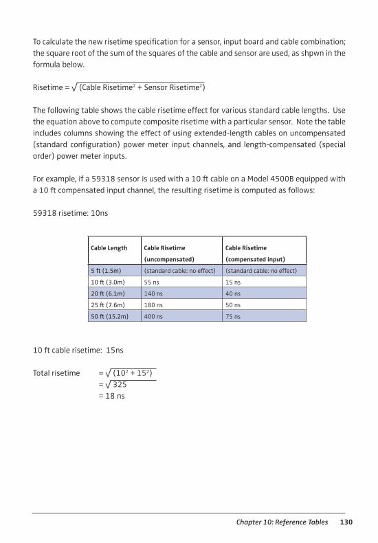
130Chapter 10: Reference Tables
To calculate the new risetime specification for a sensor, input board and cable combination; the square root of the sum of the squares of the cable and sensor are used, as shpwn in the formula below.
Risetime = √ (Cable Risetime2 + Sensor Risetime2)
The following table shows the cable risetime effect for various standard cable lengths. Use the equation above to compute composite risetime with a particular sensor. Note the table includes columns showing the effect of using extended-length cables on uncompensated (standard configuration) power meter input channels, and length-compensated (special order) power meter inputs.
For example, if a 59318 sensor is used with a 10 ft cable on a Model 4500B equipped with a 10 ft compensated input channel, the resulting risetime is computed as follows:
59318 risetime: 10ns
10 ft cable risetime: 15ns
Total risetime = √ (102 + 152) = √ 325 = 18 ns
Cable Length Cable Risetime
(uncompensated)
Cable Risetime
(compensated input)
5 ft (1.5m) (standard cable: no effect) (standard cable: no effect)
10 ft (3.0m) 55 ns 15 ns
20 ft (6.1m) 140 ns 40 ns
25 ft (7.6m) 180 ns 50 ns
50 ft (15.2m) 400 ns 75 ns
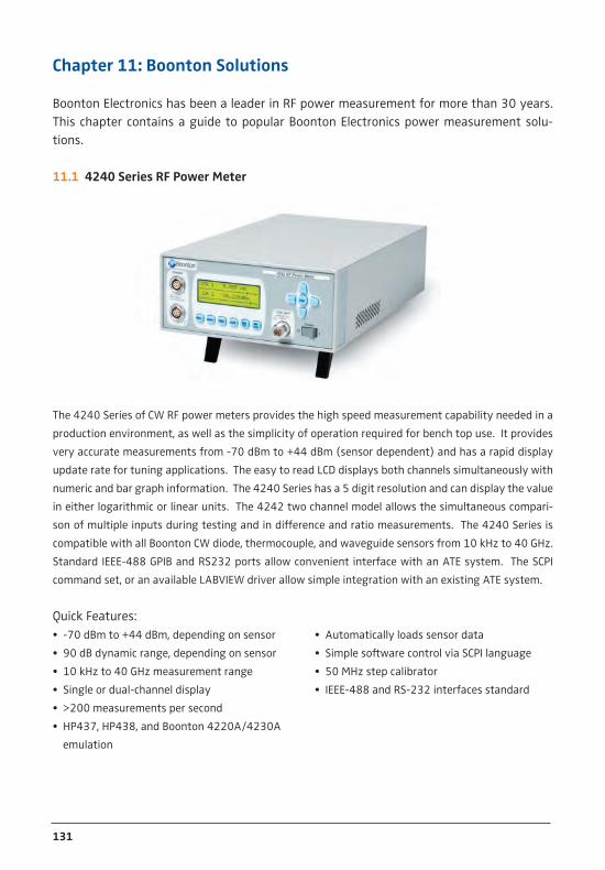
131
Chapter 11: Boonton Solutions
Boonton Electronics has been a leader in RF power measurement for more than 30 years. This chapter contains a guide to popular Boonton Electronics power measurement solu-tions.
11.1 4240 Series RF Power Meter
The 4240 Series of CW RF power meters provides the high speed measurement capability needed in a
production environment, as well as the simplicity of operation required for bench top use. It provides
very accurate measurements from -70 dBm to +44 dBm (sensor dependent) and has a rapid display
update rate for tuning applications. The easy to read LCD displays both channels simultaneously with
numeric and bar graph information. The 4240 Series has a 5 digit resolution and can display the value
in either logarithmic or linear units. The 4242 two channel model allows the simultaneous compari-
son of multiple inputs during testing and in difference and ratio measurements. The 4240 Series is
compatible with all Boonton CW diode, thermocouple, and waveguide sensors from 10 kHz to 40 GHz.
Standard IEEE-488 GPIB and RS232 ports allow convenient interface with an ATE system. The SCPI
command set, or an available LABVIEW driver allow simple integration with an existing ATE system.
Quick Features: •-70dBmto+44dBm,dependingonsensor
•90dBdynamicrange,dependingonsensor
•10kHzto40GHzmeasurementrange
•Singleordual-channeldisplay
•>200measurementspersecond
•HP437,HP438,andBoonton4220A/4230A
emulation
•Automaticallyloadssensordata
•SimplesoftwarecontrolviaSCPIlanguage
•50MHzstepcalibrator
•IEEE-488andRS-232interfacesstandard

132Chapter 11: Boonton Solutions
11.2 4530 Series RF Power Meter
The 4530 Series RF Peak Power Meter can make Peak, CW Power and RF Voltage measurements at high
speed from 10 Hz to 40 GHz (sensor dependent). Boonton’s 4530 Series RF power meters combine the
accuracy of a laboratory-grade instrument with the speed required for production test. They employ
proprietary measurement techniques that accurately measure digitally-modulated signals. Whether
you’re measuring CW power or the peak power of WCDMA or HDTV signals, Boonton’s single-channel
Model 4531 and dual-channel Model 4532 are the logical choice for high volume production test. The
4530 provides seamless CW power measurement over its broad dynamic range without the interrup-
tions and nonlinearities caused by range changes required by lesser power meters. Our thermal and
peak-power sensors never need range switching and even our CW diode sensors with 90 dB dynamic
range use only two widely overlapping ranges. The 4530 displays periodic and pulse waveforms in
graphical format, and a host of automatic measurements characterize the time and power profiles of
the pulse. As with all measurement modes, the graph display includes complete pan and zoom ability,
and can present the data in CDF, CCDF or distribution (histogram bar) formats.
Quick Features: •FrequencyRange:10kHzto40GHz
•DynamicRange:PeakPower>60dBandCWPower90dB
•Synchronous/AsynchronousTriggering
•Effectivesamplingratesupto50MSamples/sec
•Dual-channelstatisticalmeasurements(CDF/PDF)
•Modulationbandwidthto20MHz
•GPIBandRS232standardinterfacewithSCPI/RS232commands
•LABVIEWDriversavailable

133
11.3 4540 Series RF Power Meter
The Boonton model 4540 Series RF Power Meter is the instrument of choice for capturing, display-
ing and analyzing RF power in both the time and statistical domains. Applications include pulsed RF
signals such as radar, TDMA and GSM, pseudorandom or noise-like signals such as CDMA, WLAN and
WiMAX. The 4540 Series is a single or dual channel RF Power Meter that can measure modulated or CW
signals using peak and average Boonton Power sensors. The 4540 Series offers Pulse, Modulated/CW,
and Statistical operating modes, making it well suited for all requirements of R&D, manufacturing and
control operations. Single channel versions (4541) and dual channel versions (4542) are available.
The 4540 Series RF Power Meter offers an impressive detailed representation of measured signals.
This instrument is equipped with an “Auto set” feature. This feature analyzes incoming signals and
presets the instrument’s timing and trigger settings in a way that allows for immediate measure-
ments.
Quick Features: •Threeoperatingmodes:Pulse,Statistical,andModulated/CW
•HighBandwidthWideDynamicRangeSensors
•IntuitiveUserInterface
•4”colorLCDdisplay
•200pstimeresolution
•7nsrisetime
•Videobandwidthupto70MHz
•17defaultpresetsplusstoragefor25userdefinedpresets
•StatisticalanalysisincludingCCDF
•Textviewofupto14outof28parametersperchannelsimultaneously
(power / voltage, time, statistics, channel math)
•Effectivesamplingrateofupto5GSamples/secondforrepetitivesignals
•GPIB,USBandLANinterfaces

134Chapter 11: Boonton Solutions
11.4 4500B RF Peak Power Analyzer
The 4500B Peak Power Analyzer has brought the performance of peak power analyzers to a new peak
and is changing the way the industry views and analyzes RF data. The Boonton Model 4500B is the
instrument of choice for capturing, displaying, analyzing and characterizing RF power in both the time
and statistical domains. Applications include pulsed RF such as RADAR, TDMA and GSM, pseudoran-
dom or noise-like signals such as CDMA and WLAN and modulated time slotted signals such as GSM-
EDGE and TD-SCDMA. Peak power sensors are available which feature <7 nsec rise time (typical video
bandwidth up to 65 MHz) and dynamic range of 70 dB (pulse mode) or 80 dB (modulated mode).
These sensors have been optimized for use with the 4500B and are ideal for measuring RADAR, 3G
and future 4G wireless systems which use complex modulation such as OFDM. The 4500B features
optional probability density functions (PDF) and cumulative distribution functions (CDF, CCDF) to accu-
rately characterize noise-like RF such as CDMA, HDTV and WLAN. These statistical functions build and
analyze a very large population of power samples continuously at a rate of up to 25 MHz or triggered
up to 50 MHz on two channels simultaneously. These functions are fast, accurate and allow the mea-
surement of very infrequent power peaks for a user-defined population size or acquisition interval.
Quick Features: •8.4”TFTcolorLCDdisplay
•Displaysupto4measurementchannels,2memorychannelsand1mathchannelsimultaneously
•100pstimebaseresolution,10GSa/Seceffectivesamplerate
•Videobandwidthgreaterthan70MHz,typicalrisetimesto5ns(sensordependent)
•Automaticpeak-to-peak,delay-by-timeanddelay-by-eventstriggering
•Flexibletriggeringandgreaterthan80dBdynamicrange(sensordependent)
•GPIB,USBandLAN
•Textviewof15timeandpowermeasurementsperchannel
•Envelope,persistenceandrollmodedisplays
•GatedCCDFandPDFwithlogdisplay(optional)atacquisitionratesupto50MSa/s
•Continuousstatisticalanalysisofpower(optional)atacquisitionratesupto25MSa/s
•Familiaruserinterface
•PeakPowerSensorsavailablewithhighvideobandwidth,fastrisetime,andwidedynamicrange

135
11.5 Boonton CW and Peak Power SensorsCW Sensor table:
Model Frequency Range Dynamic Range1 Overload Rating Maximum SWR
Impedance Connector Pulse / Continuous Frequency SWR @ 0 dBm
Wide Dynamic Range Dual Diode Sensors
51075A
50 ohm
N (M)
500 kHz to
18 GHz
-70 to +20 dBm 1 W for 1 µs
300 mW
500 kHz to 2 GHz
2 GHz to 6 GHz
6 GHz to 18 GHz
1.15
1.20
1.40
51077A
50 ohm
N (M)
500 kHz to
18 GHz
-60 to +30 dBm 10 W for 1 µs
3 W
500 kHz to 2 GHz
2 GHz to 6 GHz
6 kHz to 18 GHz
1.15
1.20
1.40
51079A
50 ohm
N (M)
500 kHz to
18 GHz
-50 to +40 dBm 100 W for 1 µs
25 W
500 kHz to 2 GHz
2 GHz to 6 GHz
6 GHz to 18 GHz
1.15
1.20
1.40
51071A
50 ohm
K (M)
10 MHz to
26.5 GHz
-70 to +20 dBm 1 W for 1 µs
300 mW
10 MHz to 2 GHz
2 GHz to 4 GHz
4 GHz to 18 GHz
18 GHz to 26.5 GHz
1.15
1.20
1.45
1.50
51072A
50 ohm
K (M)
30 MHz to
40 GHz
-70 to +20 dBm 1 W for 1 µs
300 mW
30 MHz to 4 GHz
4 GHz to 38 GHz
38 GHz to 40 GHz
1.25
1.65
2.00
Thermoscouple Sensors
51100(9E)
50 ohm
N (M)
10 MHz to
18 GHz
-20 to +20 dBm 15 W for 1 µs
300 mW
10 MHz to 30 MHz
30 MHz to 16 GHz
16 GHz to 18 GHz
1.25
1.18
1.28
51200
50 ohm
N (M)
10 MHz to
18 GHz
0 to +37 dBm 150 W for 1 µs
10 W
10 MHz to 2 GHz
2 GHz to 12.4 GHz
12.4 kHz to 18 GHz
1.10
1.18
1.28
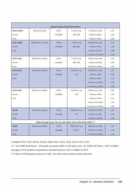
136Chapter 11: Boonton Solutions
Special Purpose Dual Diode Sensors
51011 (EMC)
50 ohm
N (M)
10 kHz to 8 GHz -60 to
+20 dBm
1 W for 1 µs
200 mW
10 kHz to 2 GHz
2 GHz to 4 GHz
4 GHz to 8 GHz
1.12
1.20
1.40
51011 (4B)
50 ohm
N (M)
100 kHz to 12.4 GHz -60 to
+20 dBm
1 W for 1 µs
300 mW
100 kHz to 2 GHz
2 GHz to 4 GHz
4 GHz to 11 GHz
11 GHz to 12.4 GHz
1.12
1.20
1.40
1.60
51013 (4E)
50 ohm
N (M)
100 kHz to 18 GHz -60 to
+20 dBm
1 W for 1 µs
300 mW
100 kHz to 4 GHz
4 GHz to 10 GHz
10 GHz to 18 GHz
1.30
1.50
1.70
51015 (5E)
50 ohm
N (M)
100 kHz to 18 GHz -50 to
+30 dBm
10 W for 1 µs
2 W
100 kHz to 1 GHz
1 GHz to 2 GHz
2 GHz to 4 GHz
4 GHz to 12.4 GHz
12.4 GHz to 18 GHz
1.07
1.10
1.12
1.18
1.28
51033 (6E)
50 ohm
N (M)
100 kHz to 18 GHz -40 to
+33 dBm
10 W for 1 µs
2 W
100 kHz to 1 GHz
1 GHz to 2 GHz
2 GHz to 4 GHz
4 GHz to 12.4 GHz
12.4 GHz to 18 GHz
1.07
1.10
1.12
1.18
1.28
51078
50 ohm
N (M)
100 kHz to 18 GHz -20 to
+37 dBm
100 W for 1 µs
7 W
100 kHz to 4 GHz
4 GHz to 12 GHz
12 GHz to 18 GHz
1.15
1.25
1.40
Diode Average Sensor (for use with 4530, 5230, 4230, 4240, 4540 **)
51085
50 ohm
N (M)
500 kHz to 18 GHz -30 to
+20 dBm
100 W for 1 µs
5 W (*)
500 kHz to 4 GHz
4 GHz to 12.4 GHz
12.4 GHz to 18 GHz
1.15
1.20
1.25
1 Models 4731, 4732, 4231A, 4232A, 4300, 4531, 4532, 5231, 5232, 5731, 5732
(*) For 51085 Peak Power - 1kW peak, 5μs pulse width, 0.25% duty cycle. For 51085 CW Power - 5W (+37dBm)
average to 25°C ambient temperature, derated linearly to 2W (+33dBm) at 85°C.
(**) Note: 4540 frequency starts at 1 MHZ. For other meters please contact Boonton.

137
Peak Sensor Table
Model Frequency Range Dynamic Rating Overload Rating Sensor Response Maximum SWR
I m p e d a n c e
Connector
(Low Bandwidth) Peak Power Range
CW Power Range
Int. Trigger Range
Pulse / Continuous Fast Risetime
(Bandwidth)
Slow Risetime
(Bandwidth)
Frequency SWR @ 0 dBm
For use with models 4500B and 4540
57006
50 ohm
N (M)
0.5 to 6 GHz
(0.05 to 6 GHz)
-50 to +20 dBm
-60 to +20 dBm
-40 to +20 dBm
1 W for 1 µs
200 mW
< 7 ns
(70 MHz
typical)
<10 µs
(350 kHz)
0.05 to 6 GHz 1.25
59318
50 ohm
N (M)
0.5 to 18 GHz
(0.05 to 18 GHz)
-24 to +20 dBm
-34 to +20 dBm
-10 to +20 dBm
1 W for 1 µs
200 mW
< 10 ns
(50 MHz
typical)
<10 µs
(350 kHz)
0.05 to 2 GHz
2 to 16 GHz
16 to 18 GHz
1.15
1.28
1.34
59340
50 ohm
K (M)
0.5 to 40 GHz
(0.05 to 40 GHz)
-24 to +20 dBm
-34 to +20 dBm
-10 to +20 dBm
1 W for 1 µs
200 mW
< 10 ns
(50 MHz
typical)
<10 µs
(350 kHz)
0.05 to 4 GHz
4 to 38 GHz
38 to 40 GHz
1.25
1.65
2.00
For use with models 4400, 4500, 4400A and 4500A Analyzers. Model 4530 with 1 GHz Calibrator Model 2530
56318
50 ohm
N (M)
0.5 to 18 GHz -24 to +20 dBm
-34 to +20 dBm
-10 to +20 dBm
1 W for 1 µs
200 mW
< 15 ns
(35 MHz
typical)
<200 ns
(1.75 MHz)
0.05 to 2 GHz
2 to 16 GHz
16 - 18 GHz
1.15
1.28
1.34
56326
50 ohm
K (M)
0.5 to 26.5 GHz -24 to +20 dBm
-34 to +20 dBm
-10 to +20 dBm
1 W for 1 µs
200 mW
< 15 ns
(35 MHz)
<200 ns
(1.75 MHz)
0.05 to 2 GHz
2 to 4 GHz
4 to 18 GHz
18 to 26.5 GHz
1.15
1.20
1.45
1.50
56518
50 ohm
N (M)
0.5 to 18 GHz -40 to +20 dBm
-50 to +20 dBm
-27 to +20 dBm
1 W for 1 µs
200 mW
< 100 ns
(6 MHz)
<300 ns
(1.16 MHz)
0.05 to 2 GHz
2 to 6 GHz
6 to 16 GHz
16 to 18 GHz
1.15
1.20
1.28
1.34
For use with models 4400, 4500, 4400A and 4500A Analyzers. Model 4530
57518
50 ohm
N (M)
0.1 to 18 GHz
(0.05 to 18 GHz)
-40 to +20 dBm
-50 to +20 dBm
-27 to +20 dBm
1 W for 1 µs
200 mW
< 100 ns
(6 MHz)
< 10 µs
(350 kHz)
0.05 - 2 GHz
2 - 16 GHz
16 - 18 GHz
1.15
1.28
1.34
57540
50 ohm
K (M)
0.1 to 40 GHz
(0.05 to 40 GHz)
-40 to +20 dBm
-50 to +20 dBm
-27 to +20 dBm
1 W for 1 µs
200 mW
< 100 ns
(6 MHz)
< 10 µs
(350 kHz)
0.05 to 4 GHz
4 to 38 GHz
38 to 40 GHz
1.25
1.65
2.00
For use with models 4500, 4400 and 4530
56218
50 ohm
N (M)
30 MHz to 18 GHz -24 to +20 dBm
-34 to +20 dBm
-10 to +20 dBm
1 W for 1 µs
200 mW
< 150 ns
(3 MHz)
< 500 ns
(700 kHz)
0.03 to 2 GHz
2 to 6 GHz
6 to 18 GHz
1.15
1.20
1.25
138Chapter 11: Boonton Solutions
For use with models 4500 and 4400
56526
50 ohm
K (M)
500 MHz to
26.5 GHz
-40 to +20 dBm
-50 to +20 dBm
-27 to +20 dBm
1 W for 1 µs
200 mW
< 100 ns
(6 MHz)
< 300 ns
(1.16 MHz)
0.03 to 2 GHz
2 to 4 GHz
4 to 18 GHz
18 to 26.5 GHz
1.15
1.20
1.45
1.50
11.6 Most Popular Peak SensorsBoonton has several popular peak power sensors and the following three are the most popular & widely used:
59340 Peak Power Sensor:
Boonton offers a very fast 59340 Peak Power Sensor for frequencies up to 40 GHz. Wireless technolo-
gy is becoming increasingly demanding for test and measurement equipment. Highly dynamic signals,
often with noise-like signal characteristics, fast switching carriers, and pulsed signals need to be ana-
lyzed accurately. Developers and engineers want reliable measurement tools to analyze such intricate
waveforms. The Boonton 59340 is the latest and fastest Peak Power Sensor operating up to 40 GHz.
Highlighted features: •OptimizedforBoonton’shighendPeakPowerMeterseries4500Band4540.
•Dynamicinputpowerrangesfrom-24dBmto+20dBminPeakmodeand
-34 dBm to +20 dBm in CW mode
•Frequenciesupto40GHz
•Risetimeoflessthan10ns
•Bandwidthupto50MHz

139
57006 Peak Power Sensor:
Boonton offers another popular and very fast Peak Power Sensor, the 57006, for frequencies up to 6
GHz. This peak power sensor is optimized for Boonton Power Meter series 4500B and 4540. It pro-
vides dynamic input power ranges from -50 dBm to +20 dBm in Peak mode and -60 dBm to +20 dBm
in CW mode. Measuring RF carrier frequencies up to 6 GHz, it has a fast 7 ns risetime response and a
video bandwidth of 70 MHz. This sensor is also ideal for statistical measurement with high dynamic
signal content due to its high speed. Frequency range is dependent upon which bandwidth the sensor
is set to. It ranges from 0.5 GHz to 6 GHz in high bandwidth mode and from 50 MHz to 6 GHz in low
bandwidth mode.
Highlighted features: •Frequenciesupto6GHz
•LowFreqRadarApplication
•CommunicationsApplications
•Bandwidthupto65MHz
•Highdynamicrange(-60to+20dBm)
•7nsrisetime(5nstypical)
•WorkwithBoonton4500Band4540Series
59318 Peak Power Sensor:
59318 Peak Power Sensor is for frequencies up to 18 GHz. This peak power sensor is also optimized for
Boonton Power Meter series 4500B and 4540. It provides dynamic input power ranges from -24 dBm
to +20 dBm in Peak mode and -34 dBm to +20 dBm in CW mode. With frequencies of up to 18 GHz,
it has a rise time of less than 10 ns and a bandwidth of up to 50 MHz. Frequency range is dependent
upon which bandwidth the sensor is set to. Usually it ranges from 0.5 GHz to 18 GHz in high band-
width mode and from 50 MHz to 18 GHz in low bandwidth mode.
Highlighted features: •Frequenciesupto18GHz
•HighFrequencyCommunicationRadarandAmplifierTesting
•10nsrisetime(8nstypical)
•44dBdynamicrangeinPeakMode
•Bandwidthupto50MHz
•WorkwithBoonton4500Band4540Series


141
25 Eastmans Rd Parsippany, NJ United States Tel: +1 973 386 9696 Fax: +1 973 386 9191 www.boonton.com
Follow us on:
WTGinnovation
Wireless Telecom Group
blog.wtcom.com
WTGinnovation
B/REFGUIDE/1111/EN Note: Specifications, terms and conditions are subject to change without prior notice.
© Copyright 2011 All rights reserved.
Scan this Code to Download a Digital Copy