product datasheet aat1239-1 switchregtm - … switchregtm 40v step-up converter for 4 to 10 white...
TRANSCRIPT

AAT1239-1
40V Step-Up Converter for 4 to 10 White LEDsSwitchRegTM
PRODUCT DATASHEET
1239-1.2008.10.1.2 1w w w . a n a l o g i c t e c h . c o m
General DescriptionThe AAT1239-1 is a high frequency, high efficiency con-stant current boost converter capable of driving up to ten (10) series-connected white LEDs or 40V. It is an ideal power solutions for backlight applications with up to ten white LEDs in series. The input voltage is 2.7V to 5.5V for single-cell lithium-ion/polymer (Li-ion) based portable devices.
The LED current is digitally controlled across a 6x oper-ating range using AnalogicTech’s Simple Serial Control™ (S2Cwire™) interface. Programmability across 26 dis-crete current steps provides high resolution, low noise, flicker-free, constant LED outputs. In programming AAT1239 operation, LED brightness increases based on the data applied at the EN/SET pin. The SEL logic pin changes the feedback voltage between two program-mable ranges.
The AAT1239-1 features a high current limit and fast, stable transitions for stepped or pulsed current applica-tions. The high switching frequency (up to 2MHz) pro-vides fast response and allows the use of ultra-small external components, including chip inductors and capacitors. Fully integrated control circuitry simplifies design and reduces total solution size. The AAT1239-1 offers a true load disconnect feature which isolates the load from the power source while in the OFF or disabled state. This eliminates leakage current, making the devic-es ideally suited for battery-powered applications.
The AAT1239-1 is available in the Pb-free, thermally-enhanced 12-pin TSOPJW package.
Features• Input Voltage Range: 2.7V to 5.5V• Maximum Continuous Output 40V @ 30mA• Drives up to 10 LEDs in Series▪ Constant LED Current with 3.5% Accuracy Over
Temperature and Input Voltage Range• Digital Control with S2Cwire Single Wire Interface▪ 26 Discrete Steps▪ No PWM Control Required▪ No Additional Circuitry
• Up to 85% Efficiency• Up to 2MHz Switching Frequency Allows Small External
Chip Inductor and Capacitors• Hysteretic Control▪ No External Compensation Components▪ Excellent Load Transient Response▪ High Efficiency at Light Loads
• Integrated Soft Start with No External Capacitor• True Load Disconnect Guarantees <1.0μA Shutdown
Current• Selectable Feedback Voltage Ranges for High Resolution
Control of Load Current• Short-Circuit, Over-Voltage, and Over-Temperature
Protection• 12-Pin TSOPJW Package• -40°C to +85°C Temperature Range
Applications• Color Display Backlight• Digital Still Cameras (DSCs)• Digital Photo Frames• PDAs and Notebook PCs • White LED Drivers
Typical Application
LIN
EN/SET
PGND
PVIN
L12.2μH
C12.2μF
C22.2μFM673Li-Ion:
VIN = 2.7V to 4.2VAAT1239-1
DS1SS16L or equivalent
R1 (RBALLAST) 30
ILED
20mA .1
SW
FB
SEL
VIN
AGND
R312k
R2374k
OVP
Enable/Set
Feedback Voltage Select
White LEDsOSRAM LW M678
or equivalent

AAT1239-1
40V Step-Up Converter for 4 to 10 White LEDsSwitchRegTM
PRODUCT DATASHEET
2 1239-1.2008.10.1.2w w w . a n a l o g i c t e c h . c o m
AAT1239-1
40V Step-Up Converter for 4 to 10 White LEDsSwitchRegTM
PRODUCT DATASHEET
2 1239-1.2008.10.1.2w w w . a n a l o g i c t e c h . c o m
Pin Descriptions
Pin # Symbol Function1 PVIN Input power pin; connected to the source of the P-channel MOSFET. Connect to the input capacitor(s).2 EN/SET IC enable pin and S2Cwire input control to set output current.
3 SEL FB voltage range select. A logic LOW sets the FB voltage range from 0.4V to 0.1V; a logic HIGH sets the FB voltage range from 0.6V to 0.3V.
4 VIN Input voltage for the converter. Connect directly to the PVIN pin.5 N/C No connection.
6, 7 SW Boost converter switching node. Connect the power inductor between this pin and LIN.8 PGND Power ground for the boost converter.9 AGND Ground pin.10 FB Feedback pin. Connect a resistor to ground to set the maximum LED current.11 OVP Feedback pin for over-voltage protection sense.12 LIN Switched power input. Connect the power inductor between this pin and SW.
Pin Configuration
TSOPJW-12(Top View)
1
2
3
4
5
6
12
11
10
9
8
7
PVIN
EN/SET
SEL
VIN
N/C
SW
LIN
OVP
FB
AGND
PGND
SW

AAT1239-1
40V Step-Up Converter for 4 to 10 White LEDsSwitchRegTM
PRODUCT DATASHEET
1239-1.2008.10.1.2 3w w w . a n a l o g i c t e c h . c o m
AAT1239-1
40V Step-Up Converter for 4 to 10 White LEDsSwitchRegTM
PRODUCT DATASHEET
1239-1.2008.10.1.2 3w w w . a n a l o g i c t e c h . c o m
Part Number Descriptions
Part NumberSEL Polarity
HIGH LOW S2C Feedback Voltage ProgrammingAAT1239ITP-1 0.6V ≥ VFB ≥ 0.3V 0.4V ≥ VFB ≥ 0.1V See Table 2
Absolute Maximum Ratings1 TA = 25°C unless otherwise noted.
Symbol Description Value UnitsPVIN, VIN Input Voltage -0.3 to 6.0 V
SW Switching Node 45 VLIN, EN/SET, SEL, FB Maximum Rating VIN + 0.3 V
TJ Operating Temperature Range -40 to 150 °CTS Storage Temperature Range -65 to 150 °C
TLEAD Maximum Soldering Temperature (at leads, 10 sec) 300 °C
Thermal Information
Symbol Description Value UnitsθJA Thermal Resistance 160 °C/WPD Maximum Power Dissipation 625 mW
1. Stresses above those listed in Absolute Maximum Ratings may cause permanent damage to the device. Functional operation at conditions other than the operating conditions specified is not implied. Only one Absolute Maximum Rating should be applied at any one time.
AAT1239-1
40V Step-Up Converter for 4 to 10 White LEDsSwitchRegTM
PRODUCT DATASHEET
4 1239-1.2008.10.1.2w w w . a n a l o g i c t e c h . c o m
AAT1239-1
40V Step-Up Converter for 4 to 10 White LEDsSwitchRegTM
PRODUCT DATASHEET
4 1239-1.2008.10.1.2w w w . a n a l o g i c t e c h . c o m
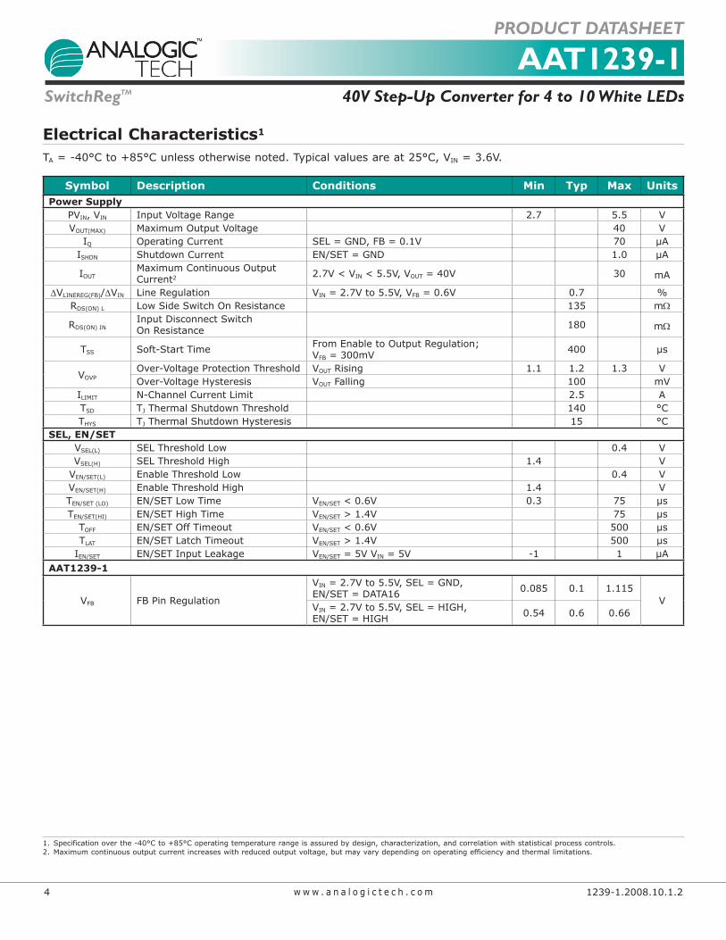
Electrical Characteristics1
TA = -40°C to +85°C unless otherwise noted. Typical values are at 25°C, VIN = 3.6V.
Symbol Description Conditions Min Typ Max UnitsPower Supply
PVIN, VIN Input Voltage Range 2.7 5.5 VVOUT(MAX) Maximum Output Voltage 40 V
IQ Operating Current SEL = GND, FB = 0.1V 70 μAISHDN Shutdown Current EN/SET = GND 1.0 μA
IOUTMaximum Continuous Output Current2 2.7V < VIN < 5.5V, VOUT = 40V 30 mA
ΔVLINEREG(FB)/ΔVIN Line Regulation VIN = 2.7V to 5.5V, VFB = 0.6V 0.7 %RDS(ON) L Low Side Switch On Resistance 135 mΩ
RDS(ON) INInput Disconnect Switch On Resistance 180 mΩ
TSS Soft-Start Time From Enable to Output Regulation; VFB = 300mV 400 μs
VOVPOver-Voltage Protection Threshold VOUT Rising 1.1 1.2 1.3 VOver-Voltage Hysteresis VOUT Falling 100 mV
ILIMIT N-Channel Current Limit 2.5 ATSD TJ Thermal Shutdown Threshold 140 °CTHYS TJ Thermal Shutdown Hysteresis 15 °C
SEL, EN/SETVSEL(L) SEL Threshold Low 0.4 VVSEL(H) SEL Threshold High 1.4 V
VEN/SET(L) Enable Threshold Low 0.4 VVEN/SET(H) Enable Threshold High 1.4 VTEN/SET (LO) EN/SET Low Time VEN/SET < 0.6V 0.3 75 μsTEN/SET(HI) EN/SET High Time VEN/SET > 1.4V 75 μs
TOFF EN/SET Off Timeout VEN/SET < 0.6V 500 μsTLAT EN/SET Latch Timeout VEN/SET > 1.4V 500 μs
IEN/SET EN/SET Input Leakage VEN/SET = 5V VIN = 5V -1 1 μA
AAT1239-1
VFB FB Pin Regulation
VIN = 2.7V to 5.5V, SEL = GND, EN/SET = DATA16 0.085 0.1 1.115
VVIN = 2.7V to 5.5V, SEL = HIGH, EN/SET = HIGH 0.54 0.6 0.66
1. Specification over the -40°C to +85°C operating temperature range is assured by design, characterization, and correlation with statistical process controls.2. Maximum continuous output current increases with reduced output voltage, but may vary depending on operating efficiency and thermal limitations.

AAT1239-1
40V Step-Up Converter for 4 to 10 White LEDsSwitchRegTM
PRODUCT DATASHEET
1239-1.2008.10.1.2 5w w w . a n a l o g i c t e c h . c o m
AAT1239-1
40V Step-Up Converter for 4 to 10 White LEDsSwitchRegTM
PRODUCT DATASHEET
1239-1.2008.10.1.2 5w w w . a n a l o g i c t e c h . c o m
Typical Characteristics
Efficiency vs. LED Current(10 White LEDs; RBALLAST = 30.1ΩΩ)
ILED (mA)
Eff
icie
ncy (
%)
66
68
70
72
74
76
78
80
2 4 6 8 10 12 14 16 18 20
VIN = 5V
VIN = 4.2V VIN = 3.6V
Efficiency vs. LED Current(9 White LEDs; RBALLAST = 30.1ΩΩ)
ILED (mA)
Eff
icie
ncy (
%)
66
68
70
72
74
76
78
2 4 6 8 10 12 14 16 18 20
VIN = 5V
VIN = 4.2V VIN = 3.6V
Shutdown Current vs. Input Voltage(EN = GND)
Input Voltage (V)
Sh
utd
ow
n C
urr
en
t (µ
A)
0.0
0.2
0.4
0.6
0.8
1.0
2.7 3.1 3.5 3.9 4.3 4.7 5.1 5.5
-40°C
85°C
25°C
Line Transient(10 White LEDs; RBALLAST = 30.1ΩΩ)
Time (50µs/div)
Inp
ut
Vo
ltag
e (
top
) (V
)
Ou
tpu
t V
olt
ag
e (
mid
dle
) (V
)
Fe
ed
ba
ck
Vo
ltag
e (b
otto
m) (V
)
32.8
33
33.2
0.58
0.6
0.62
4.2V
3.6V
Accuracy ILED vs. Input Voltage(VFB = 0.6V; RBALLAST = 30.1ΩΩ)
Input Voltage (V)
Accu
racy I
LE
D (
%)
-2.0
-1.5
-1.0
-0.5
0.0
0.5
1.0
1.5
2.0
2.7 3.2 3.7 4.2 4.7 5.2 5.7
-40°C
25°C 85°C
Accuracy ILED vs. Temperature(VFB = 0.6V; RBALLAST = 30.1ΩΩ)
Temperature (°C)
Accu
racy I
LE
D (
%)
-1.5
-1.0
-0.5
0.0
0.5
1.0
1.5
-40 -15 10 35 60 85

AAT1239-1
40V Step-Up Converter for 4 to 10 White LEDsSwitchRegTM
PRODUCT DATASHEET
6 1239-1.2008.10.1.2w w w . a n a l o g i c t e c h . c o m
AAT1239-1
40V Step-Up Converter for 4 to 10 White LEDsSwitchRegTM
PRODUCT DATASHEET
6 1239-1.2008.10.1.2w w w . a n a l o g i c t e c h . c o m
Typical Characteristics
Soft Start(10 White LEDs; VFB = 0.6V)
Time (200µs/div)
Feed
back V
olt
ag
e (
mid
dle
) (V
)
En
ab
leV
olta
ge (to
p) (V
)
Ind
uc
tor C
urre
nt (b
otto
m) (A
)
0
0.2
0.4
0.6
0
1
2
0V
3.3V
Soft Start(10 White LEDs; VFB = 0.3V)
Time (200µs/div)
Feed
back V
olt
ag
e (
mid
dle
) (V
)
En
ab
leV
olta
ge (to
p) (V
)
Ind
uc
tor C
urre
nt (b
otto
m) (A
)
0
0.2
0.4
0
1
2
0V
3.3V
0V
Shutdown(10 White LEDs; VFB = 0.6V)
Time (100µs/div)
En
ab
leV
olt
ag
e (
top
) (V
)
Feed
back V
olt
ag
e (
mid
dle
) (V
) Ind
uc
tor C
urre
nt (b
otto
m) (A
)
0
0.2
0.4
0.6
0.0
0.5
3.3V
0V
Shutdown(10 LEDs; VFB = 0.3V)
Time (50µs/div)
En
ab
leV
olt
ag
e (
top
) (V
)
Feed
back V
olt
ag
e (
mid
dle
) (V
) Ind
uc
tor C
urre
nt (b
otto
m) (A
)
0
0.2
0.4
0
0.5
3.3V
0V
Output Ripple(10 White LEDs; VIN = 3.6V; COUT = 2.2µF; ILED = 13mA)
Time (200ns/div)
VSW
(20V/div)
VOUT
(AC Coupled)
(20mV/div)
IL(500mA/div)
Output Ripple(10 White LEDs; VIN = 3.6V; COUT = 2.2µF; ILED = 20mA)
Time (200ns/div)
VSW
(20V/div)
VOUT
(AC Coupled)
(20mV/div)
IL(500mA/div)

AAT1239-1
40V Step-Up Converter for 4 to 10 White LEDsSwitchRegTM
PRODUCT DATASHEET
1239-1.2008.10.1.2 7w w w . a n a l o g i c t e c h . c o m
AAT1239-1
40V Step-Up Converter for 4 to 10 White LEDsSwitchRegTM
PRODUCT DATASHEET
1239-1.2008.10.1.2 7w w w . a n a l o g i c t e c h . c o m
Typical Characteristics
Transition of LED Current(10 White LEDs; SEL = Low; ILED = 3mA to 13mA)
Time (50µs/div)
Ou
tpu
t V
olt
ag
e (
top
) (V
)
Feed
back V
olta
ge
(bo
ttom
) (V)
28
30
32
34
0.0
0.1
0.2
0.3
0.4
Transition of LED Current(10 White LEDs; SEL = Low; ILED = 13mA to 6mA)
Time (50µs/div)
Ou
tpu
t V
olt
ag
e (
top
) (V
)
Feed
back V
olta
ge
(bo
ttom
) (V)
30
32
34
0.0
0.1
0.2
0.3
0.4
Input Disconnect Switch Resistance
vs. Input Voltage
Input Voltage (V)
RD
S(O
N)I
N (
mΩΩ
)
140
160
180
200
220
240
260
280
300
2.7 3.1 3.5 3.9 4.3 4.7 5.1 5.5
120°C
100°C
85°C25°C
Low Side Switch On Resistance
vs. Input Voltage
Input Voltage (V)
RD
S(O
N)L
(m
ΩΩ)
80
100
120
140
160
180
200
220
240
260
2.7 3.1 3.5 3.9 4.3 4.7 5.1 5.5
120°C
100°C
25°C
85°C
EN/SET Latch Timeout vs. Input Voltage
Input Voltage (V)
EN
/SE
T L
atc
h T
imeo
ut
(µs)
100
150
200
250
300
350
2.7 3.1 3.5 3.9 4.3 4.7 5.1 5.5
85°C
25°C
-40°C
EN/SET Off Timeout vs. Input Voltage
Input Voltage (V)
EN
/SE
T O
ff T
imeo
ut
(µs)
50
100
150
200
250
300
2.7 3.1 3.5 3.9 4.3 4.7 5.1 5.5
25°C85°C
-40°C

AAT1239-1
40V Step-Up Converter for 4 to 10 White LEDsSwitchRegTM
PRODUCT DATASHEET
8 1239-1.2008.10.1.2w w w . a n a l o g i c t e c h . c o m
AAT1239-1
40V Step-Up Converter for 4 to 10 White LEDsSwitchRegTM
PRODUCT DATASHEET
8 1239-1.2008.10.1.2w w w . a n a l o g i c t e c h . c o m
Typical Characteristics
Enable High Threshold (VIH) vs. Input Voltage
Input Voltage (V)
En
ab
le H
igh
Th
resh
old
(V
IH)
(V)
0.6
0.7
0.8
0.9
1.0
1.1
1.2
2.7 3.1 3.5 3.9 4.3 4.7 5.1 5.5
25°C
85°C
-40°C
Enable Low Threshold (VIL) vs. Input Voltage
Input Voltage (V)
En
ab
le L
ow
Th
resh
old
(V
IL)
(V)
0.4
0.5
0.6
0.7
0.8
0.9
1.0
1.1
1.2
2.7 3.1 3.5 3.9 4.3 4.7 5.1 5.5
25°C
85°C
-40°C

AAT1239-1
40V Step-Up Converter for 4 to 10 White LEDsSwitchRegTM
PRODUCT DATASHEET
1239-1.2008.10.1.2 9w w w . a n a l o g i c t e c h . c o m
AAT1239-1
40V Step-Up Converter for 4 to 10 White LEDsSwitchRegTM
PRODUCT DATASHEET
1239-1.2008.10.1.2 9w w w . a n a l o g i c t e c h . c o m
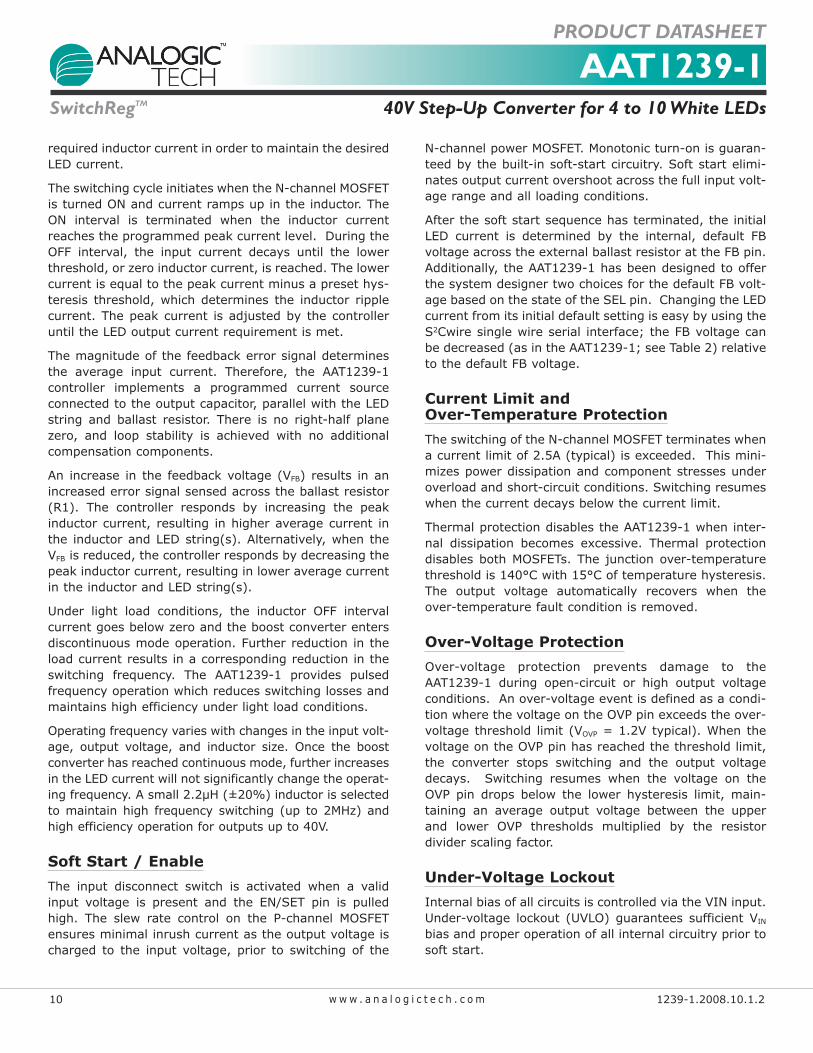
Functional DescriptionThe AAT1239-1 consists of a DC/DC boost controller, an integrated slew rate controlled input disconnect MOSFET switch, and a high voltage MOSFET power switch. A high voltage rectifier, power inductor, output capacitor, and sense resistors are required to implement a DC/DC con-stant current boost converter. The input disconnect switch is activated when a valid input voltage is present and the EN/SET pin is pulled high. The slew rate control on the P-channel MOSFET ensures minimal inrush cur-rent as the output voltage is charged to the input volt-age, prior to the switching of the N-channel power MOSFET. Monotonic turn-on is guaranteed by the inte-grated soft-start circuitry. Soft-start eliminates output voltage overshoot across the full input voltage range and all loading conditions.
The maximum current through the LED string is set by the ballast resistor and the feedback voltage of the IC. The output current may be programmed by adjusting the level of the feedback reference voltage which is pro-grammed through the S2Cwire interface. The SEL pin selects one of two feedback voltage ranges. In the AAT1239-1, the SEL function is inverted in that the FB pin voltage can be programmed from 0.4V to 0.1V with
a logic LOW applied to the SEL pin and 0.6V to 0.3V with a logic HIGH applied to the SEL pin. The feedback volt-age can be set to any one of 16 current levels within each FB range, providing high-resolution control of the LED current, using the single-wire S2Cwire control.
For some applications requiring a short duration of boosting current applying a low-to-high transition on the AAT1239-1’s SEL pin, LED current can be programmed up to 3x. The step size is determined by the programmed voltage at the FB pin where the internal default setting is 1.5x in the AAT1239-1.
Control Loop
The AAT1239-1 provides the benefits of current mode control with a simple hysteretic output current loop pro-viding exceptional stability and fast response with mini-mal design effort. The device maintains exceptional constant current regulation, transient response, and cycle-by-cycle current limit without additional compen-sation components.
The AAT1239-1 modulates the power MOSFET switching current to maintain the programmed FB voltage. This allows the FB voltage loop to directly program the
Functional Block Diagram
Control
ReferenceOutputSelect
FB
SEL
EN/SET
PVIN LIN
SW
AGND PGND
OVPVIN
AAT1239-1
40V Step-Up Converter for 4 to 10 White LEDsSwitchRegTM
PRODUCT DATASHEET
10 1239-1.2008.10.1.2w w w . a n a l o g i c t e c h . c o m
required inductor current in order to maintain the desired LED current.
The switching cycle initiates when the N-channel MOSFET is turned ON and current ramps up in the inductor. The ON interval is terminated when the inductor current reaches the programmed peak current level. During the OFF interval, the input current decays until the lower threshold, or zero inductor current, is reached. The lower current is equal to the peak current minus a preset hys-teresis threshold, which determines the inductor ripple current. The peak current is adjusted by the controller until the LED output current requirement is met.
The magnitude of the feedback error signal determines the average input current. Therefore, the AAT1239-1 controller implements a programmed current source connected to the output capacitor, parallel with the LED string and ballast resistor. There is no right-half plane zero, and loop stability is achieved with no additional compensation components.
An increase in the feedback voltage (VFB) results in an increased error signal sensed across the ballast resistor (R1). The controller responds by increasing the peak inductor current, resulting in higher average current in the inductor and LED string(s). Alternatively, when the VFB is reduced, the controller responds by decreasing the peak inductor current, resulting in lower average current in the inductor and LED string(s).
Under light load conditions, the inductor OFF interval current goes below zero and the boost converter enters discontinuous mode operation. Further reduction in the load current results in a corresponding reduction in the switching frequency. The AAT1239-1 provides pulsed frequency operation which reduces switching losses and maintains high efficiency under light load conditions.
Operating frequency varies with changes in the input volt-age, output voltage, and inductor size. Once the boost converter has reached continuous mode, further increases in the LED current will not significantly change the operat-ing frequency. A small 2.2μH (±20%) inductor is selected to maintain high frequency switching (up to 2MHz) and high efficiency operation for outputs up to 40V.
Soft Start / Enable
The input disconnect switch is activated when a valid input voltage is present and the EN/SET pin is pulled high. The slew rate control on the P-channel MOSFET ensures minimal inrush current as the output voltage is charged to the input voltage, prior to switching of the
N-channel power MOSFET. Monotonic turn-on is guaran-teed by the built-in soft-start circuitry. Soft start elimi-nates output current overshoot across the full input volt-age range and all loading conditions.
After the soft start sequence has terminated, the initial LED current is determined by the internal, default FB voltage across the external ballast resistor at the FB pin. Additionally, the AAT1239-1 has been designed to offer the system designer two choices for the default FB volt-age based on the state of the SEL pin. Changing the LED current from its initial default setting is easy by using the S2Cwire single wire serial interface; the FB voltage can be decreased (as in the AAT1239-1; see Table 2) relative to the default FB voltage.
Current Limit andOver-Temperature Protection
The switching of the N-channel MOSFET terminates when a current limit of 2.5A (typical) is exceeded. This mini-mizes power dissipation and component stresses under overload and short-circuit conditions. Switching resumes when the current decays below the current limit.
Thermal protection disables the AAT1239-1 when inter-nal dissipation becomes excessive. Thermal protection disables both MOSFETs. The junction over-temperature threshold is 140°C with 15°C of temperature hysteresis. The output voltage automatically recovers when the over-temperature fault condition is removed.
Over-Voltage Protection
Over-voltage protection prevents damage to the AAT1239-1 during open-circuit or high output voltage conditions. An over-voltage event is defined as a condi-tion where the voltage on the OVP pin exceeds the over-voltage threshold limit (VOVP = 1.2V typical). When the voltage on the OVP pin has reached the threshold limit, the converter stops switching and the output voltage decays. Switching resumes when the voltage on the OVP pin drops below the lower hysteresis limit, main-taining an average output voltage between the upper and lower OVP thresholds multiplied by the resistor divider scaling factor.
Under-Voltage Lockout
Internal bias of all circuits is controlled via the VIN input. Under-voltage lockout (UVLO) guarantees sufficient VIN bias and proper operation of all internal circuitry prior to soft start.

AAT1239-1
40V Step-Up Converter for 4 to 10 White LEDsSwitchRegTM
PRODUCT DATASHEET
1239-1.2008.10.1.2 11w w w . a n a l o g i c t e c h . c o m
Application Information
Over-Voltage Protection
OVP Protection with Open Circuit FailureThe OVP protection circuit consists of a resistor network tied from the output voltage to the OVP pin (see Figure 1). To protect the device from open circuit failure, the resistor divider can be selected such that the over-volt-age threshold occurs prior to the output reaching 40V (VOUT(MAX)). The value of R3 should be selected from 10kΩ to 20kΩ to minimize losses without degrading noise immunity.
R2 = R3 · - 1VOUT(MAX)
VOVP
⎛ ⎞⎝ ⎠
R2
R3
COUT
VOUT
AAT1239-1
OVP
GND
Figure 1: Over-Voltage Protection Circuit.
Time (4ms/div)
Ov
er
Vo
lta
ge
Pro
tec
tio
n P
in (
top
) (V
)
Ind
uc
tor
Cu
rre
nt
(bo
tto
m)(
A)
Ou
tpu
t Vo
ltag
e (m
idd
le) (V
)
1.142V
1.238V
30
40
0
2
4
Figure 2: Over-Voltage Protection Open Circuit Response (No LED).
Assume R3 = 12kΩ and VOUT(MAX) = 40V. Selecting 1% resistor for high accuracy, this results in R2 = 374kΩ (rounded to the nearest standard value). The minimum OVP threshold can be calculated:
⎛ ⎞ · + 1
⎝ ⎠VOUT(OVP_MIN) = VOVP(MIN)
= 35.4V
R2
R3
To avoid OVP detection and subsequent reduction in the programmed output current (see following section), the maximum operating voltage should not exceed the minimum OVP set point.
VOUT(MAX) < VOUT(OVP_MIN)
In some cases, this may disallow configurations with high LED forward voltage (VFLED) and/or greater than ten series white LEDs. VFLED unit-to-unit tolerance can be as high as +15% of nominal for white LED devices.
OVP Constant Voltage OperationUnder closed loop constant current conditions, the out-put voltage is determined by the operating current, LED forward voltage characteristics (VFLED), quantity of series connected LEDs (N), and the feedback pin voltage (VFB).
VOUT = VFB + N · VFLED
When the rising OVP threshold is exceeded, switching is stopped and the output voltage decays. Switching auto-matically restarts when the output drops below the lower OVP hysteresis voltage (100mV typical) and, as a result, the output voltage increases. The cycle repeats, maintaining an average DC output voltage proportional to the average of the rising and falling OVP levels (mul-tiplied by the resistor divider scaling factor). High oper-ating frequency and small output voltage ripple ensure DC current and negligible flicker in the LED string(s).
The waveform in Figure 3 shows the output voltage and LED current at cold temperature with a ten series white LED string and VOVP = 40V. As shown, the output voltage rises as a result of the increased VFLED which triggers the OVP constant voltage operation. Self heating of the LEDs triggers a smooth transition back to constant cur-rent control.

AAT1239-1
40V Step-Up Converter for 4 to 10 White LEDsSwitchRegTM
PRODUCT DATASHEET
12 1239-1.2008.10.1.2w w w . a n a l o g i c t e c h . c o m
VOUT
(5V/div)
ILED
(200mA/div)
Self-RecoveryCold Temperature Apply
Over-Voltage Protection
Figure 3: Over-Voltage Protection Constant Voltage Operation
(10 White LEDs; ILED = 20mA; R2 = 12kΩ; R3 = 374kΩ).
While OVP is active, the maximum LED current program-ming error (ΔILED) is proportional to voltage error across an individual LED (ΔVFLED).
(N · VFLED(TYP) - VOUT(OVP_MIN) - VFB)
N
ΔVFLED =
To minimize the ΔILED error, the minimum OVP voltage (VOUT(OVP_MIN)) may be increased, yielding a corresponding increase in the maximum OVP voltage (VOUT(OVP_MAX)). Measurements should confirm that the maximum switch-ing node voltage (VSW(MAX)) is less than 45V under worst-case operating conditions.
⎛ ⎞ · + 1 + VF + VRING⎝ ⎠VSW(MAX) = VOVP(MAX)
R3
R2
VF = -Schottky Diode DS1 forward voltage at turn-OFF
VRING = Voltage ring occurring at turn-OFF
LED Selection and Current Setting
The AAT1239-1 is well suited for driving white LEDs with constant current. Applications include main and sub-LCD display backlighting, and color LEDs.
The LED current is controlled by the FB voltage and the ballast resistor. For maximum accuracy, a 1% tolerance resistor is recommended.
The ballast resistor (RBALLAST) value can be calculated as follows:
VFB(MAX)
ILED(MAX)
RBALLAST =
where:
VFB(MAX) = 0.4V when SEL = Low
VFB(MAX) = 0.6V when SEL = High
i.e., for a maximum LED current of 20mA (SEL = High):
VFB
ILED(MAX)
0.6
0.020RBALLAST = = = 30Ω ≈ 30.1Ω
Maximum ILED
Current (mA)RBALLAST (Ω)
SEL = High SEL = Low
30 20.0 13.325 24.3 16.220 30.1 20.015 40.2 26.710 60.4 40.25 121.0 80.6
Table 1: Maximum LED Current and RBALLAST Resistor Values (1% Resistor Tolerance).
Typical white LEDs are driven at maximum continuous currents of 15mA to 20mA. The maximum number of series connected LEDs is determined by the minimum OVP voltage of the boost converter (VOUT(OVP_MIN)), minus the maximum feedback voltage (VFB(MAX)) divided by the maximum LED forward voltage (VFLED(MAX)). VFLED(MAX) can be estimated from the manufacturers’ datasheet at the maximum LED operating current.
⎛ ⎞ · + 1
⎝ ⎠VOUT(OVP_MIN) = VOVP(TYP)
R2
R3
(VOUT(OVP_MIN) - VFB(MAX))
VFLED(MAX)
N =
Figure 4 shows the schematic of using ten LEDs in series. Assume VFLED @ 20mA = 3.5V (typical) from LW M673 (OSRAM) datasheet.
⎛ ⎞ · + 1
⎝ ⎠VOUT(OVP_MIN) = 1.2V = 38.6V374kΩ10.4kΩ
38.6V - 0.6V
3.5VN =
≈ 10.9
Therefore, under these typical operating conditions, ten LEDs can be used in series.

AAT1239-1
40V Step-Up Converter for 4 to 10 White LEDsSwitchRegTM
PRODUCT DATASHEET
1239-1.2008.10.1.2 13w w w . a n a l o g i c t e c h . c o m
LED Brightness Control
The AAT1239-1 uses S2Cwire programming to control LED brightness and does not require PWM (pulse width modulation) or additional control circuitry. This feature greatly reduces the burden on a microcontroller or sys-tem IC to manage LED or display brightness, allowing the user to “set it and forget it.” With its high-speed serial interface (1MHz data rate), the output current of the AAT1239-1 can be changed successively to brighten or dim the LEDs in smooth transitions (i.e., to fade out) or in abrupt steps, giving the user complete program-mability and real-time control of LED brightness.
0
5
10
15
20
25
1 4 7 10 13 16
S2Cwire Data Register
LE
D C
urr
en
t (m
A)
SEL=HIGH
SEL=LOW
Default
Figure 5: Programming AAT1239-1 LED Current with RBALLAST = 30.1Ω.
C12.2μF
2.2μHL1
374KR2
12KR3
R1
30.1
VCC
123
Enable
JP1 10KR4
2.2μFC2
123
Select
JP2
DS1
under 20V application: C2 25V 0805 X7R 2.2μF GRM21BR71E225KA73L
C1 10V 0603 X5R 2.2μF GRM188R60J225KE01D
DS1 SS16L
N/C5
VIN1
SW6PGND 8
EN2
SEL3
SW 7
VP4 GND 9FB 10
OVP 11LIN 12
AAT1239-1 TSOP12JW
U1
LEDD1
LEDD2
LEDD3
LEDD4
LEDD5LED
D9
L1 2.2μH SD3814-2R2 or SD3110-2R2
LEDD6
LEDD7
LEDD8
LEDD10
C2 50V 1206 X7R 2.2μF GRM31CR71H225KA88
other alternatives:more stability at 40V: C2 50V 1206 X7R 4.7μF GRM31CR71H475K
D1-D10 LW M673 White LED
Figure 4: AAT1239-1 White LED Boost Converter Schematic.

AAT1239-1
40V Step-Up Converter for 4 to 10 White LEDsSwitchRegTM
PRODUCT DATASHEET
14 1239-1.2008.10.1.2w w w . a n a l o g i c t e c h . c o m
Alternatively, toggling the SEL logic pin from low to high implements stepped or pulsed LED currents by increas-ing the FB pin voltage. Figure 6 illustrates the SELECT pin scaling factor, defined as the LED current with SEL=HIGH divided by the LED current with SEL=LOW. In the AAT1239-1, the possible scaling factors are 3.0x to 1.5x with the internal default setting of 1.5x.
S2Cwire Data Register
Sele
ct P
in S
calin
g Fa
ctor
(Low
to H
igh)
(Default)
1.0
1.5
2.0
2.5
3.0
3.5
1 4 7 10 13 16
Figure 6: AAT1239-1 SEL Pin Scaling Factor:ILED (SEL = High) Divided by ILED (SEL = Low).
S2Cwire Serial Interface
AnalogicTech’s S2Cwire single wire serial interface is a proprietary high-speed single-wire interface available only from AnalogicTech. The S2Cwire interface records
rising edges of the EN/SET input and decodes them into 16 individual states. Each state corresponds to a refer-ence feedback voltage setting on the FB pin, as shown in Table 2.
S2Cwire Serial Interface Timing
The S2Cwire single wire serial interface data can be clocked-in at speeds up to 1MHz. After data has been submitted, EN/SET is held high to latch the data for a period TLAT. The FB pin voltage is subsequently changed to the level as defined by the state of the SEL logic pin. When EN/SET is set low for a time greater than TOFF, the AAT1239-1 is disabled. When the AAT1239-1 is disabled, the register is reset to its default value. In the AAT1239-1, the FB pin voltage is set to 0.3V if the EN/SET pin is subsequently pulled HIGH.
S2Cwire Feedback Voltage Programming
The FB pin voltage is set to the default level at initial powerup. The AAT1239-1 is programmed through the S2Cwire interface. Table 2 illustrates FB pin voltage pro-gramming for the AAT1239-1. The rising clock edges applied at the EN/SET pin determine the FB pin voltage. If a logic LOW is applied at the SEL pin of the AAT1239-1, the default feedback voltage range becomes 0.4V to 0.1V and 0.6V to 0.3V for a logic HIGH condition at the SEL pin.
1
EN/SET2 n-1 n ≤ 16
Data Reg 0 n-1 0
THI
TLO TLAT TOFF
Figure 7: AAT1239-1 S2Cwire Timing Diagram to Program the Output Voltage.

AAT1239-1
40V Step-Up Converter for 4 to 10 White LEDsSwitchRegTM
PRODUCT DATASHEET
1239-1.2008.10.1.2 15w w w . a n a l o g i c t e c h . c o m
Selecting the Schottky Diode
To ensure minimum forward voltage drop and no recov-ery, high voltage Schottky diodes are considered the best choice for the AAT1239-1 boost converter. The out-put diode is sized to maintain acceptable efficiency and reasonable operating junction temperature under full load operating conditions. Forward voltage (VF) and package thermal resistance (θJA) are the dominant fac-tors to consider in selecting a diode. The diode non-re-petitive peak forward surge current rating (IFSM) should be considered for high pulsed load applications, such as camera flash. IFSM rating drops with increasing conduc-tion period. Manufacturers’ datasheets should be con-sulted to verify reliability under peak loading conditions. The diode’s published current rating may not reflect actual operating conditions and should be used only as a comparative measure between similarly rated devices.
40V rated Schottky diodes are recommended for outputs less than 30V, while 60V rated Schottky diodes are rec-ommended for outputs greater than 35V.
The switching period is divided between ON and OFF time intervals.
= TON + TOFF
1
FS
During the ON time, the N-channel power MOSFET is conducting and storing energy in the boost inductor. During the OFF time, the N-channel power MOSFET is not conducting. Stored energy is transferred from the input battery and boost inductor to the output load through the output diode.
Duty cycle is defined as the ON time divided by the total switching interval.
TON
TON + TOFF
D =
= TON ⋅ FS
Rising Clock Edges/Data
Register
SEL = Low SEL = High
Reference Voltage (V)
LED Current (mA); RBALLAST = 30.1Ω
Reference Voltage (V)
LED Current (mA); RBALLAST = 30.1Ω
1 0.4 (default) 13.29 0.6 (default) 19.932 0.38 12.62 0.58 19.273 0.36 11.96 0.56 18.604 0.34 11.30 0.54 17.945 0.32 10.63 0.52 17.286 0.30 9.97 0.50 16.617 0.28 9.30 0.48 15.958 0.26 8.64 0.46 15.289 0.24 7.97 0.44 14.6210 0.22 7.31 0.42 13.9511 0.20 6.64 0.40 13.2912 0.18 5.98 0.38 12.6213 0.16 5.32 0.36 11.9614 0.14 4.65 0.34 11.3015 0.12 3.99 0.32 10.6316 0.10 3.32 0.30 9.97
Table 2: AAT1239-1 S2Cwire Reference Feedback Voltage Control Settings With RBALLAST = 30.1Ω (Assumes Nominal Values)*.
*All table entries are preliminary and subject to change without notice.

AAT1239-1
40V Step-Up Converter for 4 to 10 White LEDsSwitchRegTM
PRODUCT DATASHEET
16 1239-1.2008.10.1.2w w w . a n a l o g i c t e c h . c o m
The maximum duty cycle can be estimated from the relationship for a continuous mode boost converter. Maximum duty cycle (DMAX) is the duty cycle at minimum input voltage (VIN(MIN)).
VOUT - VIN(MIN)
VOUT
DMAX =
The average diode current is equal to the output current.
IAVG(TOT) = IOUT
The average output current multiplied by the forward diode voltage determines the loss of the output diode.
PLOSS(DIODE) = IAVG(TOT) · VF
= IOUT · VF
For continuous LED currents, the diode junction tem-perature can be estimated.
TJ(DIODE) = TAMB + θJA · PLOSS(DIODE)
Output diode junction temperature should be maintained below 110ºC, but may vary depending on application and/or system guidelines. The diode θJA can be mini-mized with additional PCB area on the cathode. PCB heat-sinking the anode may degrade EMI performance. The reverse leakage current of the rectifier must be con-sidered to maintain low quiescent (input) current and
high efficiency under light load. The rectifier reverse cur-rent increases dramatically at elevated temperatures.
Selecting the Boost Inductor
The AAT1239-1 controller utilizes hysteretic control and the switching frequency varies with output load and input voltage. The value of the inductor determines the maxi-mum switching frequency of the boost converter. Increased output inductance decreases the switching fre-quency and switching loss, but results in higher peak currents and increased output voltage ripple. To maintain 2MHz maximum switching frequency and stable opera-tion, an output inductor sized from 1.5μH to 2.7μH is recommended. For higher efficiency in Li-ion battery applications (VIN from 3.0V to 4.2V) and stable operation, increasing the inductor size up to 10μH is recommended. Figure 15 and 16 show the special enhanced efficiency application.
A better estimate of DMAX is possible once VF is known.
(VOUT + VF - VIN(MIN))
(VOUT + VF)
DMAX =
Where VF is the Schottky diode forward voltage. If not known, it can be estimated at 0.5V.
Manufacturer’s specifications list both the inductor DC current rating, which is a thermal limitation, and peak inductor current rating, which is determined by the satu-ration characteristics. Measurements at full load and high ambient temperature should be completed to ensure that the inductor does not saturate or exhibit excessive temperature rise.
ManufacturerPart
Number
Rated Forward Current
(A)
Non-RepetitivePeak SurgeCurrent (A)
Rated Voltage
(V)
Thermal Resistance (θJA, °C/W)
Size (mm)(LxWxH) Case
Taiwan Semiconductor Co., Ltd.
SS16L1.1
30 60 45 3.8x1.9x1.43 Sub SMASS15L 30 50 45 3.8x1.9x1.43 Sub SMASS14L 30 40 45 3.8x1.9x1.43 Sub SMA
Diodes, Inc B340LA 3 70.0 40 25 5.59x2.92x2.30 SMA
Zetex ZHCS350 0.35 4.2 40 330 1.7x0.9x0.8 SOD523
Table 3: Typical Surface Mount Schottky Rectifiers for Various Output Levels.

AAT1239-1
40V Step-Up Converter for 4 to 10 White LEDsSwitchRegTM
PRODUCT DATASHEET
1239-1.2008.10.1.2 17w w w . a n a l o g i c t e c h . c o m
AAT1239-1
40V Step-Up Converter for 4 to 10 White LEDsSwitchRegTM
PRODUCT DATASHEET
1239-1.2008.10.1.2 17w w w . a n a l o g i c t e c h . c o m
The output inductor (L) is selected to avoid saturation at minimum input voltage, maximum output load condi-tions. Peak current may be estimated using the follow-ing equation, assuming continuous conduction mode. Worst-case peak current occurs at minimum input volt-age (maximum duty cycle) and maximum load. Switching frequency (FS) can be estimated from the curves and assumes a 2.2μH inductor.
IOUT
(1 - DMAX)
DMAX · VIN(MIN)
(2 · FS · L)
IPEAK = +
At light load and low output voltage, the controller reduces the operating frequency to maintain maximum operating efficiency. As a result, further reduction in output load does not reduce the peak current. Minimum peak current can be estimated from 0.5A to 0.75A.
At high load and high output voltages, the switching fre-quency is somewhat diminished, resulting in higher IPEAK. Bench measurements are recommended to confirm actu-al IPEAK and ensure that the inductor does not saturate at maximum LED current and minimum input voltage.
The RMS current flowing through the boost inductor is equal to the DC plus AC ripple components. Under worst-case RMS conditions, the current waveform is critically continuous. The resulting RMS calculation yields worst-case inductor loss. The RMS current value should
be compared against the manufacturer’s temperature rise, or thermal derating, guidelines.
IPEAK IRMS =
3
For a given inductor type, smaller inductor size leads to an increase in DCR winding resistance and, in most cases, increased thermal impedance. Winding resistance degrades boost converter efficiency and increases the inductor’s operating temperature.
PLOSS(INDUCTOR) = IRMS2 · DCR
To ensure high reliability, the inductor case temperature should not exceed 100ºC. In some cases, PCB heatsink-ing applied to the LIN node (non-switching) can improve the inductor’s thermal capability. PCB heatsinking may degrade EMI performance when applied to the SW node (switching) of the AAT1239-1.
Shielded inductors provide decreased EMI and may be required in noise sensitive applications. Unshielded chip inductors provide significant space savings at a reduced cost compared to shielded (wound and gapped) induc-tors. In general, chip-type inductors have increased winding resistance (DCR) when compared to shielded, wound varieties.
Manufacturer Part Number Inductance
(μH) Maximum DC ISAT
Current (mA)DCR(mΩ)
Size (mm)LxWxH Type
Sumidawww.sumida.com
CDRH2D14-2R2 2.2 1500 75 3.2x3.2x1.55 Shielded CDRH2D14-4R7 4.7 1000 135 3.2x3.2x1.55 Shielded
CDRH4D22/HP-4R7 4.7 2200 66 5.0x5.0x2.4 ShieldedCDRH3D18-100NC 10 900 164 4.0x4.0x2.0 Shielded
Cooper Electronicswww.cooperet.com
SD3814-2R2 2.2 1900 77 4.0x4.0x1.0 ShieldedSD3110-2R2 2.2 910 161 3.1x3.1x1.0 ShieldedSD3118-4R7 4.7 1020 162 3.1x3.1x1.8 ShieldedSD3118-100 10 900 295 3.1x3.1x1.8 Shielded
Taiyo Yudenwww.t-yuden.com
NP03SB-2R0M 2 1900 32 4.0x4.0x1.8 ShieldedNR3010T-2R2M 2.2 1100 95 3.0x3.0x1.0 Shielded
NP03SB4R7 4.7 1200 47 4.0x4.0x1.8 ShieldedNP03SB100M 10 800 100 4.0x4.0x1.8 Shielded
Table 4: Recommended Inductors for Various Output Levels (Select IPEAK < ISAT).

AAT1239-1
40V Step-Up Converter for 4 to 10 White LEDsSwitchRegTM
PRODUCT DATASHEET
18 1239-1.2008.10.1.2w w w . a n a l o g i c t e c h . c o m
Inductor Efficiency Considerations
The efficiency for different inductors is shown in Figure 8 for ten white LEDs in series. Smaller inductors yield increased DCR and reduced operating efficiency.
63
66
69
72
75
2 5 8 11 14 17 20
LED Current (mA)
Eff
icie
ncy (
%)
CDRH5D16F-2R2 (29mΩ)
SD3814-2R2 (77mΩ)
Figure 8: AAT1239-1 Efficiency for Different Inductor Types (VIN = 3.6V;
Ten White LEDs in Series).
Selecting the Boost Capacitors
The high output ripple inherent in the boost converter necessitates low impedance output filtering.
Multi-layer ceramic (MLC) capacitors provide small size and adequate capacitance, low parasitic equivalent series resistance (ESR) and equivalent series inductance (ESL), and are well suited for use with the AAT1239-1 boost regulator. MLC capacitors of type X7R or X5R are
recommended to ensure good capacitance stability over the full operating temperature range.
The output capacitor is sized to maintain the output load without significant voltage droop (ΔVOUT) during the power switch ON interval, when the output diode is not conducting. A ceramic output capacitor from 2.2μF to 4.7μF is recommended (see Table 5). Typically, 50V rated capacitors are required for the 40V maximum boost output. Ceramic capacitors sized as small as 0805 or 1206 are available which meet these requirements.
MLC capacitors exhibit significant capacitance reduction with applied voltage. Output ripple measurements should confirm that output voltage droop and operating stability are acceptable. Voltage derating can minimize this fac-tor, but results may vary with package size and among specific manufacturers.
Output capacitor size can be estimated at a switching frequency (FS) of 500kHz (worst case).
IOUT · DMAX
FS · ΔVOUT
COUT =
To maintain stable operation at full load, the output capacitor should be sized to maintain ΔVOUT between 100mV and 200mV.
The boost converter input current flows during both ON and OFF switching intervals. The input ripple current is less than the output ripple and, as a result, less input capacitance is required.
Manufacturer Part Number Value (μF) Voltage Rating Temp Co Case SizeMurata GRM188R60J225KE19 2.2 6.3 X5R 0603Murata GRM188R61A225KE34 2.2 10 X5R 0603Murata GRM21BR71E225KA73L 2.2 25 X7R 0805Murata GRM31CR71H225KA88 2.2 50 X7R 1206Murata GRM31CR71H475K 4.7 50 X7R 1206
Table 5: Recommended Ceramic Capacitors.

AAT1239-1
40V Step-Up Converter for 4 to 10 White LEDsSwitchRegTM
PRODUCT DATASHEET
1239-1.2008.10.1.2 19w w w . a n a l o g i c t e c h . c o m
AAT1239-1
40V Step-Up Converter for 4 to 10 White LEDsSwitchRegTM
PRODUCT DATASHEET
1239-1.2008.10.1.2 19w w w . a n a l o g i c t e c h . c o m
PCB Layout Guidelines
Boost converter performance can be adversely affected by poor layout. Possible impact includes high input and output voltage ripple, poor EMI performance, and reduced operating efficiency. Every attempt should be made to optimize the layout in order to minimize para-sitic PCB effects (stray resistance, capacitance, and inductance) and EMI coupling from the high frequency SW node. A suggested PCB layout for the AAT1239-1 boost converter is shown in Figures 9 and 10. The fol-lowing PCB layout guidelines should be considered:
1. Minimize the distance from Capacitor C1 and C2 negative terminal to the PGND pins. This is espe-cially true with output capacitor C2, which conducts high ripple current from the output diode back to the PGND pins.
2. Minimize the distance between L1 to DS1 and switching pin SW; minimize the size of the PCB area connected to the SW pin.
3. Maintain a ground plane and connect to the IC PGND pin(s) as well as the GND terminals of C1 and C2.
4. Consider additional PCB area on DS1 cathode to maximize heatsinking capability. This may be neces-sary when using a diode with a high VF and/or ther-mal resistance.
5. To avoid problems at startup, add a 10kΩ resistor between the VIN, VP and EN/SET pins (R4). This is critical in applications requiring immunity from input noise during “hot plug” events, e.g. when plugged into an active USB port.
Figure 9: AAT1239-1 Evaluation Figure 10: AAT1239-1 Evaluation Board Top Side Layout (with ten LEDs Board Bottom Side Layout (with ten LEDs and microcontroller). and microcontroller).

AAT1239-1
40V Step-Up Converter for 4 to 10 White LEDsSwitchRegTM
PRODUCT DATASHEET
20 1239-1.2008.10.1.2w w w . a n a l o g i c t e c h . c o m
AAT1239-1
40V Step-Up Converter for 4 to 10 White LEDsSwitchRegTM
PRODUCT DATASHEET
20 1239-1.2008.10.1.2w w w . a n a l o g i c t e c h . c o m
U1AAT1239-1
C14.7μF
VIN1
EN2
LINOVP
12
11
SEL3
VP4
5 N/C6
SW
FBGND
PGNDSW
10
9
8
7
VCCJP11 2 3
DC+DC- L110μH
R312k
R2374k
DS1Schottky
C10μF
C22.2μF
VOUT
30.1Ω
R1
D1WLED
D2WLED
D3WLED
D4WLED
D5WLED
D7WLED
D8WLED
D9WLED
D10WLED
U2PIC12F675VDD
1
GP52
3 GP44
GP3
VSSGP0GP1
GP2
8
7
6
5
JP2 JP3
R4
10k
C30.1μF
R9330Ω
D11Green
R61k
R51k
R71k
VCC
R8330Ω
D12Red
Up
Down
Select
AAT1239-1White LED
Driver
S2CwireMicrocontroller
D6WLED
JP4
S1
S2
S3
Figure 11: AAT1239-1 Evaluation Board Schematic (with ten LEDs and microcontroller).

AAT1239-1
40V Step-Up Converter for 4 to 10 White LEDsSwitchRegTM
PRODUCT DATASHEET
1239-1.2008.10.1.2 21w w w . a n a l o g i c t e c h . c o m
AAT1239-1
40V Step-Up Converter for 4 to 10 White LEDsSwitchRegTM
PRODUCT DATASHEET
1239-1.2008.10.1.2 21w w w . a n a l o g i c t e c h . c o m
Additional Applications
C12.2μF
PVIN
VIN
LIN
SW
PGND
EN/SET
SEL
OVP
FB
AGND
L12.2μH
R312k
R2158k
DS1Schottky
C22.2μF
Up to 17V/30mA max
D1LED
D2LEDD3
LED
D4LED
Li-IonVIN = 2.7V to 5.5V AAT1239-1
R130.1Ω 20mA
Efficiency vs. LED Current(4 White LEDs; RBALLAST = 30.1ΩΩ)
ILED (mA)
Eff
icie
ncy (
%)
74
75
76
77
78
79
80
81
82
83
84
2 4 6 8 10 12 14 16 18 20
VIN = 5V
VIN = 4.2V VIN = 3.6V
Figure 12: Four LEDs In Series Configuration.
C12.2μF
PVIN
VIN
LIN
SW
PGND
EN/SET
SEL
OVP
FB
AGND
L12.2μH
R312k
R2287k
DS1Schottky
C22.2μF
Up to 30V/30mA max
D1LED
D2LEDD3
LED
D4LED
Li-IonVIN = 2.7V to 5.5V AAT1239-1
R130.1Ω 20mA
D5LED
D6LED
D7LED
D8LED
Efficiency vs. LED Current(8 White LEDs; RBALLAST = 30.1ΩΩ)
ILED (mA)
Eff
icie
ncy (
%)
66
68
70
72
74
76
78
80
2 4 6 8 10 12 14 16 18 20
VIN = 5V
VIN = 4.2V VIN = 3.6V
Figure 13: Eight LEDs In Series Configuration.
C12.2μF
PVIN
VIN
LIN
SW
PGND
EN/SET
SEL
OVP
FB
AGND
L12.2μH
R312k
R2324k
DS1Schottky
C22.2μF
Up to 34V/30mA max
D1LED
D2LEDD3
LED
D4LED
Li-IonVIN = 2.7V to 5.5V AAT1239-1
R130.1Ω 20mA
D5LED
D6LED
D7LED
D8LED
D9LED
Efficiency vs. LED Current(9 White LEDs; RBALLAST = 30.1ΩΩ)
ILED (mA)
Eff
icie
ncy (
%)
66
68
70
72
74
76
78
2 4 6 8 10 12 14 16 18 20
VIN = 5V
VIN = 4.2V VIN = 3.6V
Figure 14: Nine LEDs In Series Configuration.

AAT1239-1
40V Step-Up Converter for 4 to 10 White LEDsSwitchRegTM
PRODUCT DATASHEET
22 1239-1.2008.10.1.2w w w . a n a l o g i c t e c h . c o m
AAT1239-1
40V Step-Up Converter for 4 to 10 White LEDsSwitchRegTM
PRODUCT DATASHEET
22 1239-1.2008.10.1.2w w w . a n a l o g i c t e c h . c o m
C1 10V 0805 X5R 4.7μF GRM219R61A475KE19C2 50V 1206 X7R 2.2μF GRM31CR71H225KA88L1 10μH CDRH3D18-100NCDS1 SS16L
C14.7μF
PVIN
VIN
LIN
SW
PGND
EN/SET
SEL
OVP
FB
AGND
L110μH
R312kΩ
R2374kΩ
DS1
C22.2μF
Li-IonVIN = 3.0V to 4.2V AAT1239-1
R130.1Ω 20mA
D10 D9 D8 D7
D6
D5
D4
D3
D2
D1
IOUT (mA)
Effic
ienc
y (%
)
2 4 6 8 10 12 14 16 18 2070.0
72.5
75.0
77.5
80.0
82.5
85.0
87.5
90.0
VIN = 3.0VVIN = 3.6V VIN = 4.2V
Figure 15: Enhanced Efficiency Configuration for Li-ion Battery Ten WLEDs Series-Connected Application.
C1 10V 0805 X5R 4.7μF GRM219R61A475KE19C2 50V 1206 X7R 2.2μF GRM31CR71H225KA88L1 4.7μH CDRH4D22/HP-4R7DS1 SS16L
C14.7μF
PVIN
VIN
LIN
SW
PGND
EN/SET
SEL
OVP
FB
AGND
L14.7μH
R312kΩ
R2374kΩ
DS1
C22.2μF
Li-IonVIN=3.0V to 4.2V AAT1239 -1
R115Ω 40mA
D1
D3
D2
D4
D5
D6
D7
D8
D11
D13
D12
D14
D15
D16
D17
D18
D9
D10
D19
D20
IOUT (mA)
Effic
ienc
y (%
)
5 10 15 20 25 30 35 4065.0
67.5
70.0
72.5
75.0
77.5
80.0
82.5
85.0
VIN = 3.0VVIN = 3.6V VIN = 4.2V
Figure 16: Enhanced Efficiency Configuration for Li-ion Battery, Two Branch,Ten WLEDs Series-Connected Application.

AAT1239-1
40V Step-Up Converter for 4 to 10 White LEDsSwitchRegTM
PRODUCT DATASHEET
1239-1.2008.10.1.2 23w w w . a n a l o g i c t e c h . c o m
AAT1239-1
40V Step-Up Converter for 4 to 10 White LEDsSwitchRegTM
PRODUCT DATASHEET
1239-1.2008.10.1.2 23w w w . a n a l o g i c t e c h . c o m
Advanced Analogic Technologies, Inc.3230 Scott Boulevard, Santa Clara, CA 95054Phone (408) 737-4600Fax (408) 737-4611
© Advanced Analogic Technologies, Inc.AnalogicTech cannot assume responsibility for use of any circuitry other than circuitry entirely embodied in an AnalogicTech product. No circuit patent licenses, copyrights, mask work rights, or other intellectual property rights are implied. AnalogicTech reserves the right to make changes to their products or specifi cations or to discontinue any product or service without notice. Except as provided in AnalogicTech’s terms and conditions of sale, AnalogicTech assumes no liability whatsoever, and AnalogicTech disclaims any express or implied warranty relating to the sale and/or use of AnalogicTech products including liability or warranties relating to fi tness for a particular purpose, merchantability, or infringement of any patent, copyright or other intellectual property right. In order to minimize risks associated with the customer’s applications, adequate design and operating safeguards must be provided by the customer to minimize inherent or procedural hazards. Testing and other quality control techniques are utilized to the extent AnalogicTech deems necessary to support this warranty. Specifi c testing of all parameters of each device is not necessarily performed. AnalogicTech and the AnalogicTech logo are trademarks of Advanced Analogic Technologies Incorporated. All other brand and product names appearing in this document are registered trademarks or trademarks of their respective holders.
Ordering Information
Package Marking1 Part Number (Tape and Reel)2
TSOPJW-12 ZLXYY AAT1239ITP-1-T1
All AnalogicTech products are offered in Pb-free packaging. The term “Pb-free” means semiconductor products that are in compliance with current RoHS standards, including the requirement that lead not exceed 0.1% by weight in homogeneous materials. For more information, please visit our website at http://www.analogictech.com/about/quality.aspx.
Package Information
TSOPJW-12
0.20 + 0.10 - 0.05
0.055 ± 0.045 0.45 ± 0.15
7° NOM
4° ± 4°
3.00 ± 0.10
2.40
± 0
.10
2.85
± 0
.20
0.50 BSC 0.50 BSC 0.50 BSC 0.50 BSC 0.50 BSC
0.15
± 0
.05
0.96
25 ±
0.0
375
1.00
+ 0
.10
- 0
.065
0.04 REF
0.010
2.75 ± 0.25
All dimensions in millimeters.
1. XYY = assembly and date code.2. Sample stock is generally held on part numbers listed in BOLD.