production of carbon nanotubes by pecvd and their...
TRANSCRIPT

Production of Carbon Nanotubes by PECVD and Their Applications to Supercapacitors Burak Caglar
-1-
Production of Carbon Nanotubes by PECVD and
Their Applications to Supercapacitors
Burak Caglar
Prof. Enric Bertran and Dr. Eric Jover, Department of Applied Physics and Optics and Institute Nanoscience
and Nanotechnology, IN2UB, Universitat de Barcelona, C/ Marti i Franques, 1, 08028, Barcelona, Spain
Abstract— Plasma enhanced chemical vapor deposition
(PECVD) is a versatile technique to obtain vertically dense-
aligned carbon nanotubes (CNTs) at lower temperatures than
chemical vapor deposition (CVD). In this work, we used
magnetron sputtering to deposit iron layer as a catalyst on silicon
wafers. After that, radio frequency (rf) assisted PECVD reactor
was used to grow CNTs. They were treated with water plasma
and finally covered by MnO2 as dielectric layer in order to use
CNTs as electrode for supercapacitors. Optimization of
annealing time, reaction time and temperature, water plasma
time and MnO2 deposition time were performed to find
appropriate conditions to improve the characteristics of
supercapacitors. SEM (Scanning Electron Microscopy), TEM
(Transmission Electron Microscopy), AFM (Atomic Force
Microscopy) and Raman spectroscopy were used to characterize
obtained electrodes.
Index Terms—5.Nanostructured Materials: Plasma Enhanced
Chemical Vapor Deposition (PECVD), Carbon Nanotubes
(CNTs), Magnetron Sputtering, Supercapacitor
I. INTRODUCTION
ANOTECHNOLOGY is the construction and use of
functional structures designed from atomic or
molecular scale with at least one characteristic
dimension in nanometer range. Their size allows them
to exhibit novel and significantly improved physical,
chemical, and biological properties because of their size.
When characteristic structural features are intermediate
between isolated atoms and bulk materials in the range of
about one to 100 nanometers, the objects often display
physical attributes substantially different from those displayed
by either atoms or bulk materials [1]. Nanotechnology is
going to change the world and the way we live, creating new
scientific applications that are smaller, faster, stronger, safer
and more reliable [2]. As impressive as nanotechnology
might be, there are also potential disadvantages; potential
mass poisoning over a period of time or incredibly small
particles that may very well cause eventual health problems in
the consumers that use them [3].
(a) (b)
Fig. 1. (a) Schematic diagram showing how a hexagonal sheet of graphite is
„rolled‟ to form a carbon nanotube (b) Illustrations of the atomic structure of
an armchair, a zig-zag and a chiral nanotube [4].
A. Carbon Nanotubes
Carbon nanotubes are built from sp2 carbon units and
consist of honeycomb lattices and are a seamless structure.
They are tubular having a diameter of a few nanometers (b)
but lengths of many microns. MWCNTs are closed graphite
tubules rolled like a graphite sheet. Diameters usually range
between 2 and 25 nm and single-walled carbon nanotubes’
(SWCNT) are made of a single seamlessly rolled graphite
sheet with a typical diameter of about 1.4 nm which is similar
to a buckyball (C60). They have a tendency to form in bundles
which are parallel in contact and consist of tens to hundreds of
nanotubes. Depending on how the graphene walls of the
nanotube are rolled together they can result in an armchair,
zigzag or chiral shapes (fig.1b). These groups are
distinguished by their unit cells which are determined by the
chiral vector given by the equation: Ch= na1 + ma2 where a1
and a2 are unit vectors in the two-dimensional hexagonal
lattice, and n and m are integers as seen in fig.1a. Another
important parameter is the chiral angle, which is the angle
between Ch and a1. When n = m and the chiral angle is 300
degrees it is known as an armchair type. When m or n are zero
and the chiral angle is equal to zero the nanotube is known as
zigzag. Chiral nanotubes are therefore when the chiral angles
are between 0o and 30
o.
N
Armchair
Zig-Zag

Production of Carbon Nanotubes by PECVD and Their Applications to Supercapacitors Burak Caglar
-2-
a. Properties
Carbon nanotubes (CNTs) are unique nanostructures which
are known to have remarkable electronic and mechanical
properties. These characteristics have sparked great interest in
their possible uses for nano-electronic and nano-mechanical
devices. CNTs have elastic modulus of greater than 1 TPa
(that of a diamond is 1.2 TPa) and strength 10–100 times
higher than the strongest steel at a fraction of the weight. They
can conduct electric current carrying capacity 1000 times
higher than copper wires. The nanotubes were found to have
an extremely large breaking strain which decreased with
temperature [4]. In the π-tight-binding model within the zone-
folding scheme, one third of the nanotubes are metallic and
two thirds are semiconducting depending on their indices (n,
m) [5]. On the other hand, carbon nanotubes that arise during
the production process may induce oxidative stress and
prominent pulmonary inflammation [6]. Studies collectively
show that regardless of the process by which CNTs were
synthesized and the types and amounts of metals they
contained, CNTs were capable of producing inflammation,
epithelioid granulomas (microscopic nodules), fibrosis, and
biochemical/toxicological changes in the lungs [7]. The
needle-like fiber shape of CNTs, similar to asbestos fibers,
raises fears that widespread use of carbon nanotubes may lead
to mesothelioma, cancer of the lining of the lungs often caused
by exposure to asbestos [8]. Although further research is
required, results presented today clearly demonstrate that,
under certain conditions, especially those involving chronic
exposure, carbon nanotubes can pose a serious risk to human
health. Therefore, their use has to assess the whole life cycle
of the product and its proper disposal.
b. Applications
The unique properties of both the single-walled and multi-
walled varieties of carbon nanotubes have led to several
studies in modern physics, resulting in applications in a wide
variety of materials and devices [9]. CNTs’ small size with
larger surface area, high sensitivity and fast response to gas
molecules and good reversibility at room temperature enable
them as a gas molecule sensors, high electrical conductivity,
and chemical stability make them good electron emitters,
carbon nanotubes are also being considered for energy storage
and production because of their small dimensions, a smooth
surface topology, and perfect surface specificity [4], they are
also used in scanning probe tips or as a composite on airplane
wings and fuselages.
c. Supercapacitors
Electrochemical double-layer capacitors, also known as
supercapacitors or ultracapacitors, are electrical storage
devices, which have a relatively high energy storage density
simultaneously with a high power density.
Fig. 2. Electrochemical double-layer capacitors [11]
Recent developments in basic technology, materials and
manufacturability have made supercapacitors an imperative
tool for short term energy storage in power electronics.
Supercapacitors consist of two electrodes immersed in or
impregnated with an electrolyte solution with a semi-
permeable membrane serving as a separator that prevents
electrical contact between the two electrodes, but which
allows for ionic diffusion (fig. 2). When an electric potential is
applied to the electrodes, a potential difference is created at
the electrode-electrolyte interface. This electrostatic interface
consists of a double layer between ions in the electrolyte and
the electronic charges on the electrode.
There are several reasons why CNT-based electrodes
perform prosperously in supercapacitors. Nanotubes have high
conductivity, large surface area (1 to >2000 m2/g), good
corrosion resistance, high temperature stability, percolated
pore structure, and can be functionalized to optimize their
properties [10].
Multi-walled (MWCNTs) and single-walled carbon
nanotubes (SWCNTs) have been already proposed as
electrode materials for supercapacitors. Different values of
specific capacitance depend mainly on the kind and purity of
samples. Generally, for highly purified nanotubes, i.e. without
other carbon forms and residual catalyst, specific capacitance
varies from 15 to 80 F/g of nanotubular material. Pure carbon
nanotubes possess a very high surface area from 120 to 400
m2/g due to their highly mesoporous character connected with
entanglement and/or presence of central canal. Generally, the
more graphitized nanotubes the smaller values of capacitance.
On the other hand, presence of defects causes an increase in
the ability of accumulating of charges. It is well known that
charging of electrical double layer proceeds mainly in the
access of solvated ions through micropores of electrode
whereas mesopores play an important transportation role as
well as, adsorption. Hence, enhancement of nanotubes

Production of Carbon Nanotubes by PECVD and Their Applications to Supercapacitors Burak Caglar
-3-
microporosity is of great interest for supercapacitor
application but also for other electrochemical application
(hydrogen storage, support for catalyst). An improvement of
capacitance can be realized by increasing the electrode surface
area of nanotubes or by pseudofaradaic effects obtained by the
addition of special oxides or conducting polymers [12].
Manganese can be present in various valence states, and its
oxides are promising candidates for electrochemical
capacitors (ECs) because of their low cost and being
environmentally friendly [13]. Because of these several
reasons, in this work, it was decided to deposit MnO2 onto the
obtained CNTs in order to improve their behavior.
B. Production Methods
a. CVD (Chemical Vapor Deposition)
The CVD method (fig.3) uses a carbon source in the gas
phase and plasma or a resistively heated coil, to transfer the
energy to the gaseous carbon molecule. The commonly used
carbon sources are CH4, CO2 and C2H2. The process
temperature cracks the molecule into atomic carbon. The
carbon then diffuses toward the substrate, which is heated and
coated with a catalyst (usually a first row transition metal such
as Ni, Fe, or Co) and binds to it [14]. CNTs are formed in this
procedure if the proper parameters are maintained such as the
temperature and the pressure of operation, the volume and
concentration of carbon sources, the size and the pretreatment
of metallic catalyst, and the time of reaction [4].
Control over the diameter as well as the growth rate of the
nanotubes is achieved by CVD method. Use of an appropriate
metal catalyst permits the preferential growth of SWCNTs
rather than MWCNTs. CVD synthesis of nanotubes is
essentially a two-step process, consisting of a catalyst
preparation step followed by the actual synthesis of the
nanotube. The catalyst is generally prepared by sputtering a
transition metal onto a substrate and then using etching by
chemicals such as ammonia or thermal annealing to induce the
nucleation of catalyst particles. Thermal annealing results in
metal cluster formation on the substrate, from which the
nanotubes grow. The temperature for the synthesis of
nanotubes by CVD is generally in the 650-900°C range [14].
Fig. 3. Schematic of CVD [15]
To eliminate impurities formed during the process such as
graphite compounds, amorphous carbon, fullerenes, coal and
metal nanoparticle, purification is needed. This is achieved by
oxidative treatments in the gaseous phase, liquid phase, acid
treatment, micro filtration, thermal treatment and ultrasound
methods [4].
b. Arc Discharge
The arc discharge method (fig.4), initially used for
producing C60 fullerenes, is the most common and perhaps
easiest way to produce CNTs as it is rather simple to
undertake. However, it is a technique that produces a mixture
of components and requires separating nanotubes from the
soot and the catalytic metals present in the crude product [16].
In this method an electric arc discharge is generated
between two graphite electrodes under inert atmosphere of
helium or argon. A very high temperature is obtained which
allows the sublimation of the carbon. For the carbon
nanotubes to be obtained, purification by gasification with
oxygen or carbon dioxide is needed. For single wall nanotubes
to be obtained a metal catalyst is needed. Process parameters
involve small gaps between electrodes (~1 mm), high current
(100 A), plasma between the electrode at about 4000 K and
voltage range (30–35 V) under specified electrode dimensions
[4].
Fig. 4. Arc Discharge [4]
Fig. 5. Laser Ablation [4]
Growing nanotubes
Copper
collector Laser Beam
Furnace
Argon gas Graphite Target

Production of Carbon Nanotubes by PECVD and Their Applications to Supercapacitors Burak Caglar
-4-
c. Laser Ablation
A pulsed or continuous laser (fig.5) is used to vaporize a
graphite target in an oven at 1200oC. The oven is filled with
helium or argon gas in order to keep the pressure at 500Torr
(6,7x10⁴Pa). A hot vapor plume forms, then expands and
cools rapidly.
As the vaporized species cool, small carbon molecules and
atoms quickly condense to form larger clusters, possibly
including fullerenes. The catalysts also begin to condense, but
more slowly at first, and attach to carbon clusters and prevent
their closing into cage structures. Catalysts may even open
cage structures when they attach to them. From these initial
clusters, tubular molecules grow into SWCNTs until the
catalyst particles become too large, or until conditions have
cooled sufficiently that carbon no longer can diffuse through
or over the surface of the catalyst particles [14].
d. PECVD (Plasma Enhanced Chemical Vapor Deposition)
The plasma-enhanced CVD (PECVD) method involves a
glow discharge in a chamber or a reaction furnace through a
high-frequency voltage applied to both the electrodes. Fig. 6
shows a schematic diagram of a typical PECVD apparatus
with a parallel plate electrode structure. A substrate is placed
on the grounded electrode. In order to form a uniform film, the
reaction gas is supplied from the opposite plate. Catalytic
metals such as Fe, Ni, and Co are used on a Si or SiO2
substrate using thermal CVD or sputtering. After the
nanoscopic fine metal particles are formed, the CNTs grow on
the metal particles on the substrate by the glow discharge
generated from a high-frequency power source. A carbon-
containing gas, such as C2H2, CH4, C2H4, C2H6, or CO is
supplied to the chamber during the discharge. The catalyst has
a strong effect on the nanotube diameter, growth rate, wall
thickness, morphology, and microstructure [14].
In ordinary CVD processes, films are formed purely through
thermochemical reactions at the substrate surface from gases
in the ground state. The reaction progresses under nearly
thermodynamic equilibrium. On the other hand, PECVD is a
film formation technique that causes excited species to react
with each other in the gas phase. This makes it possible to
deposit films at lower substrate temperatures than with
thermal CVD, in which a high substrate temperature is
necessary to cross over the activation energy.
In order to generate a discharge for cold plasma, low
pressure is of course required. PECVD is, however, a film
formation process which includes chemical reactions.
Therefore, higher particle density of active species is required
in order to get higher deposition rates. The pressure range in
PECVD lies between 0.1 and 10 Torr. Mean-free path of gas
particles at this pressure range are as short as several hundred
micrometers [17].
Fig. 6. Schematic of PECVD [14]
The growth of CNTs using PECVD is a very complicated
process because it involves many determining factors in
growth conditions. These important factors involve the
catalytic material, the catalytic support material (namely,
catalyst–substrate interactions), the growth temperature
gradient across the catalytic particle and the effect of plasma.
Compared with conventional CVD, plasma-enhanced
chemical vapor deposition (PECVD) is advantageous for the
direct growth of CNTs on the substrates at a relatively low
growth temperature and also large area fabrication of CNTs
due to the presence of an uniform plasma [18].
It is easier to fabricate aligned CNTs, at lower substrate
temperature by using PECVD technique. Various plasma
sources have been used for the growth of CNT such as
microwave, direct current, and inductive coupled radio
frequency. However, these sources are not suited for the large
area deposition, because it is difficult to generate an uniform
plasma for a large area. However, capacitive coupled radio
frequency PECVD (rf-PECVD) method has a possibility for
the large area deposition, because the plasma is very stable
and homogeneous. However, the quality of CNT synthesized
by rf-PECVD method is comparatively poor; for example, it is
covered with large amount of carbon soot, it has a low aspect
ratio and a stacked-cone structure [19].
C. CNTs Growth Mechanism
Quantum molecular dynamics simulations have been
reported to understand the growth process of MWCNTs [20].
Within such calculations, the topmost atoms (dangling bonds)
of the inner and outer edges of a bilayer tube rapidly move
towards each other, forming several bonds to bridge the gap
between the adjacent edges, thus verifying the assumption that
atomic bridges could keep the growing edge of a nanotube
open without the need of ―spot-weld‖ adatoms.
Hot Filament

Production of Carbon Nanotubes by PECVD and Their Applications to Supercapacitors Burak Caglar
-5-
Fig. 7. (a) Spontaneous closure of SWNTs at ~3000K (b) Open-ended growth
of MWNTs stabilized by “lip-lip” interactions at ~3000K [20]
Fig. 8. Close-ended catalytic growth of SWCNTs at ~1500K [20]
(a) (b)
Fig. 9. (a) First step: segregation of carbon at the nano-particle surface when
cooling from 2000K to 1500K (b) Second step: nucleation and growth of a
carbon nanotube germ extruding from a large catalytic nanoparticle [20].
At ~3000K (a typical experimental growth temperature), the
―lip-lip‖ interactions stabilize the open-ended bilayer structure
(fig.7) and inhibit the spontaneous dome closure of the inner
tube as observed in analogous simulations of single-shell
tubes. These calculations also show that this end geometry is
highly active chemically, and easily accommodates incoming
carbon clusters, supporting a model of growth by
chemisorption from the vapor phase [20]. The catalytic growth
of SWNTs (fig.8 & 9) was investigated using first-principles
molecular dynamics simulations. At experimental
temperatures (~1500K), even though the open end of
SWCNTs closes spontaneously into a graphitic dome, the
metal-carbon chemical bonds keep breaking and reforming.
Such phenomenon provides a direct incorporation process for
the necessary additional carbon, and suggests a close-end
mechanism for the catalytic growth. The catalytic action of
metallic atoms is also found to play a key role in the
reconstruction of the nanotube tip after carbon incorporation,
by annihilation of defects. The short range action of the metal
may explain the relatively narrow diameter observed for
SWCNTs [20].
The nucleation and growth of SWCNTs within a root
growth mechanism (where carbon atoms precipitate from
particles larger than the tube diameter) was studied using
quantum molecular dynamics simulations. It was suggested
that carbon atoms can be added at the root of a growing tube
by a diffusion-segregation process occurring at the surface of
the catalytic particle [20].
II. THE GOAL OF THESIS
The main objective of this work is to optimize the
production of Carbon Nanotubes (CNTs) as base material for
supercapacitors using PECVD. Therefore, we will try to
maximize the surface-area characteristics and electrical
properties of obtained CNTs.
In order to achieve this, several milestones should be
reached:
Optimization of the catalyst layer thickness and
annealing time in order to obtain a homogenate and desired
catalyst particle formation.
Optimization of the PECVD operating parameters
(reaction time and temperature) to grow dense and long CNTs.
Optimization of the CNTs purification by means of
water plasma in order to remove amorphous carbon from the
CNTs samples and to open the tips of CNTs increasing their
specific area.
III. EXPERIMENTAL
A. Reactor
This section explains all reaction steps with details.
CNTs production was carried out in PECVD reactor which
was developed by the FEMAN group as a result of the
European Project NANOTUBE. This reactor has 3 homemade
magnetron sputtering heads that permit to deposit materials
onto wafers without taking them out of the system. All
operations are controlled with especially designed LabView
software (version 7.1, National Instruments, USA). To heat
the system during annealing and PECVD, Xantrex (XDC 60-
100, Digital DC power supply, Canada) heater is used. As
vacuum plays an important role in sputtering and PECVD
processes, 3 types of pumps are used in the reactor. From
atmospheric pressure to ~2 x 10³ Pa or lower, rotatory pump
(EV25 QS AL, Laybold Vacuum GmbH, Germany) is used,
from ~2 x 10³ to ~3 x 10
-2 Pa Root pump (WU 251, Leybold
Heraus RUVAC, Germany) and from ~3 x 10⁻²
to ~4 x 10⁻⁴
Pa
Turbamolecular pump is used (Turbovac 361C, Leybold
Vacuum GmbH, Germany).
a. Sample Preparation
In PECVD process, CNTs were grown onto Si wafers.
These wafers are p-type boron doped Silicon (Si) and their
resistivity is between 0.01 to 0.02 Ω cm-1
(4482/R, SI-MAT,

Production of Carbon Nanotubes by PECVD and Their Applications to Supercapacitors Burak Caglar
-6-
Germany). They were prepared in the size of 1.5 cm x 1 cm.
To introduce Si samples into the reactor, graphite holders
were used. Another Si wafer was attached onto graphite with
silver paint to obtain better thermal contact between holder
and sample.
b. Sputtering
Nanometric transition metal particles (Fe, Co, Ni, Pd. . .)
are indispensable to catalyze CNT growth when using
PECVD methods. That has been generally done by physical
vapor deposition (PVD) techniques, magnetron sputtering or
patterned by electron lithography methods. Anyhow, catalyst
deposition is an auxiliary step in PECVD grown CNTs [21].
In sputtering process (fig.10), magnetron was used to create
magnetic field which is parallel to the cathode and plasma was
generated by radio frequency which was the energy source
used between anode and cathode, so it is called rf-magnetron
sputtering. Fe was chosen as catalyst and Ar as precursor gas
(128 sccm, achieving 2 Pa), the process was operated at 50 W
(TIS 0.5/13560, Huttinger, Germany), For the first time
operation of Fe target, there is need to calibrate it. This
calibration was performed by depositing Fe layer during 30
min. onto glass sample and checking its thickness in AFM.
After that, by dividing this thickness to 30 min. deposition rate
of Fe target was calculated for 1 min. and then sputtering time
for process was obtained for desired Fe thickness. For the
optimized conditions, 91 s sputtering were needed to obtain a
resulting 3 nm thickness Fe layer.
c. Annealing
Annealing is a crucial step where prepared Fe layer is
cracked into nanometric Fe-islands (fig.11). These
nanoislands will be the origin of CNT growth and it is
necessary to obtain homogenous island dispersion on wafer. In
our case, Fe layer was heated up to several temperatures
between 650oC and 850
oC and kept during 2 min. H2 gas (Air
Liquide, France) was used at 2 mbar and 100 sccm to keep a
reducing atmosphere and avoid Fe oxidation.
Fig. 10. Sputtering heads
d. Reaction (PECVD)
The special design of the reactor (fig.12) permits to send
directly the wafer from annealing to reaction position. In this
way, contact of Fe layer with air and its potential oxidation
was prevented.
Fig. 11. Fe layer after annealing
Fig. 12. Reactor: From left to right; place to introduce sample inside the
chamber and 4 different heads; 2 for Fe and Si sputtering, 1 for heater and
PECVD reaction and last one is free.

Production of Carbon Nanotubes by PECVD and Their Applications to Supercapacitors Burak Caglar
-7-
Reaction parameters are shown in the table;
TABLE I.
PECVD REACTION PARAMETERS
Precursor Gas* NH3
Flow rate 100 sccm
Carbon Source** C2H2
Flow Rate 50 sccm
Purge pressure 0.8 mbar
Reaction Pressure 1 mbar
Plasma Power 50 W
Reaction Temperature 650 to 850oC
Reaction Time 600 to 1200 s
* (Conc.99.9%, Linde, Germany) ** (Conc.99.6%, Praxair, Spain)
After obtaining an appropriate dispersion of Fe nanoislands
on Si wafer, the process of CNTs growth can start. Fig.13
shows, the PECVD reaction diagram and a micrograph of the
resulting CNTs.
Fig. 13. Reaction diagram and CNTs photo after PECVD
e. Water plasma
Growth of CNTs with PECVD reaction causes the presence
of amorphous carbon on the obtained CNTs and this should be
removed to increase the deposit specific area of CNTs and to
improve their electron transfer capability. Another advantage
of water plasma application is to cut off tips of CNTs where
Fe catalyst particles exist. Opening tips of CNTs would supply
more surface area for applications.
This procedure was operated at 50W, 50Pa H2O plasma and
during 30, 60 and 300 s.
B. Characterization Methods
In this work, several characterization methods were used. In
this section, a brief description was given and role of Atomic
force microscopy (AFM), Transmission and Scanning electron
microscopies (TEM, SEM) and Raman spectroscopy methods
were explained. As well as for checking morphology of CNTs,
these helpful tools were also used for some specific aims.
AFM imaging is performed by scanning a very sharp tip
across the sample surface while the force of interaction
between the tip and the sample is monitored at pN sensitivity.
The sample is mounted on a piezoelectric scanner which
ensures three-dimensional positioning with high resolution,
and the force between tip and surface is monitored by
measuring the cantilever deflection using an optical method
(laser, photodiode) [22].
In this study we used a Park Systems XE series AFM
(South Korea). During studies, non-contact mode was used to
keep safe the cantilever tip and measurements were seen and
interpreted with Ueye (version 2.40.0005) and XEI (version
1.7.3) software. Moreover, AFM was used to calibrate the
catalyst deposition rate.
SEM is a type of electron microscope that images the
sample surface by scanning it with a high-energy beam of
electrons in a raster scan pattern. The electrons interact with
the atoms that make up the sample producing signals that
contain information about the surface topography of sample,
composition and other properties such as electrical
conductivity.
The signal produced by SEM includes secondary electrons,
back-scattered electrons (BSE), characteristic X-rays, light
(cathodoluminescence), specimen current and transmitted
electrons. Secondary electron detectors are common in all
SEMs, but it is rare that a single machine would have
detectors for all possible signals [23].
In this work, SEM was used to check the dispersion and
diameter of the Fe particles after the annealing step and to
characterize the CNTs morphology. The system is HITACHI
S 2300 type SEM (Japan) and it belongs to University of
Barcelona’s Serveis Cientifico-Tecnics (SCT-UB).
TEM is a microscopy technique whereby a beam of
electrons is transmitted through an ultra thin specimen,
Production of Carbon Nanotubes by PECVD and Their Applications to Supercapacitors Burak Caglar
-8-
interacting with the specimen as it passes through. An image
is formed from the interaction of the electrons transmitted
through the specimen; the image is magnified and focused
onto an imaging device, such as a fluorescent screen, on a
layer of photographic film, or to be detected by a sensor such
as a CCD camera.
TEMs are capable of imaging at a significantly higher
resolution than optic microscopes, owing to the small de
Broglie wavelength of electrons. This enables the instrument's
user to examine fine detail—even as small as a single column
of atoms, which is tens of thousands times smaller than the
smallest resolvable object in an optic microscope [24].
Philips CM-30 (The Netherlands) type TEM that was used
for this project belongs to SCT-UB.
Raman spectroscopy relies on inelastic scattering, or Raman
scattering, of monochromatic light, usually from a laser in the
visible, near infrared, or near ultraviolet range. The laser light
interacts with phonons or other excitations in the system,
resulting in the energy of the laser photons being shifted up or
down. The shift in energy gives information about the phonon
modes in the system. Typically, a sample is illuminated with a
laser beam. Light from the illuminated spot is collected with a
lens and sent through a monochromator. Wavelengths close to
the laser line, due to elastic Rayleigh scattering, are filtered
out while the rest of the collected light is dispersed onto a
detector. Finally, an obtained spectrum is interpreted
according to peaks and materials they belong to [25].
HORIBA Jobin Yvon T 64000 (Japan) type Raman
machine that also belongs to SCT-UB, was used to check the
presence of carbon and oxygen in prepared samples by
PECVD and also MnO2 deposition on CNTs which was
performed to enhance the capacitance of supercapacitor.
C. Electrochemical Deposition & Characterization
This part of work was performed in AUTOLAB
(89/336/EEC, Eco Chemie B.V, The Netherlands). Using this
system, CNTs were coated with a MnO2 layer which will
perform as a dielectric layer in the supercapacitor. Based on a
homemade experimental set up, electrochemical
characterization of previously obtained CNTs samples was
carried out. Capacitance behavior of samples was studied with
cyclic voltammetry (CV) and obtained spectra interpreted area
of samples was calculated using CV. To examine capacitance
values of electrodes, charge-discharge experiment results and
related formulas were used. Operational details of both the
electrochemical deposition and the electrochemical
characterization are included in the Mr. Toygan Mutlu’s
master thesis.
IV. RESULTS & DISCUSSION
A. Optimization of Annealing Time
Annealing time is a crucial parameter to obtain low
diameter homogenously dispersed catalyst particles. These
nanoislands of catalyst will strongly influence the
characteristics of the CNTs which will grow on them. To
optimize the annealing time of Fe catalyst particles, other
parameters were held constant; catalyst thickness as 5 nm,
PECVD reaction time as 900 s and reaction temperature as
750oC.
In annealing process, system went up to 750oC at different
times (ramp time) and was kept at this temperature during
120 s (hold time). Annealing time was taken as sum of these 2
values and it was assigned like; 10 min., 14.5 min. and 30 min.
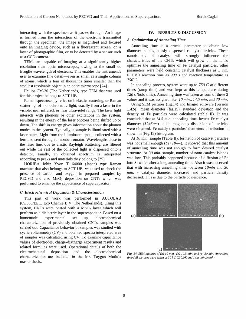
Using SEM pictures (fig.14) and ImageJ software (version
1.42q), mean diameter (fig.15), standard deviation and the
density of Fe particles were calculated (table II). It was
concluded that at 14.5 min. annealing time, lowest Fe catalyst
diameter (32±8nm) and homogenous dispersion of particles
were obtained. Fe catalyst particles’ diameters distribution is
shown in (Fig.15) histogram.
At 10 min. sample (Table II), formation of catalyst particles
was not small enough (51±10nm). It showed that this amount
of annealing time was not enough to form desired catalyst
structure. At 30 min. sample, number of nano catalyst islands
was low. This probably happened because of diffusion of Fe
into Si wafer after a long annealing time. Also it was observed
that with increasing annealing time -between 10min and 30
min. - catalyst diameter increased and particle density
decreased. This is due to the particle coalescence.
(a) (b)
(c) Fig. 14. SEM pictures of (a) 10 min., (b) 14.5 min. and (c) 30 min. Annealing
time (all pictures were taken at 30 kV, X30.0K and 1μm unit length)

Production of Carbon Nanotubes by PECVD and Their Applications to Supercapacitors Burak Caglar
-9-
TABLE II
PROPERTIES OF FE CATALYST PARTICLES
Samples
Fe catalyst diameter
(nm)
Fe catalyst
nanoparticles
(in 12 μm2 area)
10 min. 51±10 1259
14.5 min. 32±8 3415
30 min. 83±20 913
* 12 μm2 is the surface area which was observed by SEM. Comparison of
Fe catalyst density was performed calculating mean number of particles in
this unit area.
Fig. 15. The histogram of Fe catalyst particle diameter
B. Optimization of Catalyst Thickness & PECVD Reaction
Temperature
As well as homogeneity and well dispersion of Fe catalyst,
also its thickness has important role in CNTs growth. Besides
this parameter, another crucial point is temperature
dependence of PECVD reaction even if there is no need to
reach as high temperature as in CVD process. Plasma ambient
makes possible to obtain CNTs at lower temperatures.
In this case, it was decided to optimize both catalyst
thickness and reaction temperature at the same time. For this,
Box-Wilson experimental design was adapted for chosen
parameter values. To perform experiments, 13 conditions were
chosen according to Box-Wilson graph distribution (Fig.16).
Fig. 16. Box-Wilson experimental design samples distribution
The use of this experimental design enables to optimize
simultaneously two operating parameters taking into
consideration also the possible interactions between these two
parameters. The central point of the experimental design was
replicated 5 times in order to evaluate the intrinsic standard
deviation of the process.
In Box-Wilson design; Diameter, length, density and
alignment of CNTs were evaluated as dependent variables
(Table III). The goal was to obtain dense, vertically aligned
long and thin CNTs. In this way, a second degree polynomial
equation including the first level interactions was developed
for each dependent variable:
TttTtTDiameter 5
2
4
2
3210 (1)
Where, T is the PECVD temperature, t is thickness of Fe
catalyst layer and αn are coefficients obtained by statistically
adjusting these polynomial equations.
In Fig.17 we can see how temperature is significantly
negatively correlated (p<0.01) with the density of the obtained
CNTs. Therefore the denser deposits are obtained at lower
temperatures. The first interaction coefficient (AB) is also
significant from a statistical point of view and positively
correlated with the density. After adjusting the eq. 1 we
obtained the following equation:
TttTtTDiameter 01.006.00001.05.811.08.2 22
This model is statistically significant (p<0.05) and explains
85% of the samples variation. For some of the dependent
variables the statistical correlations were not so clear and in
these cases explained sample variation is lower. This is due to
the high internal variation observed for the central point
(between 11 to 28% depending on the parameter) which
increases the complexity of the evaluation.
Fe layer thickness (nm)

Production of Carbon Nanotubes by PECVD and Their Applications to Supercapacitors Burak Caglar
-10-
Table III
SUMMARY OF THE OBTAINED EXPERIMENTAL RESULTS BASED ON SEM IMAGES TREATMENT
# Temperature
(ºC)
Fe layer
thickness
(nm)
CNTs
diameter
(nm)
Fe
diameter†
(nm)
Length
(µm) Density
* Alignment
*
1 680 7.0 72 82 6.8 7 7.5
2 750 5.0 -**
-**
-**
-**
-**
3 820 3.0 133 100 3.6 1 0.0
4 750 5.0 95 69 2.5 5 5.0
5 849 5.0 -**
-**
-**
-**
-**
6 820 7.0 64 -**
0.5 5 0.0
7 651 5.0 72 37 3.9 7 7.5
8 750 5.0 104 90 3.8 6 5.0
9 750 5.0 93 76 5 4 2.5
10 750 2.2 -**
-**
-**
-**
-**
11 680 3.0 59 13 7.4 9 10.0
12 750 5.0 64 80 4.5 6 5.0
13 750 7.8 114 43 3.1 6 5.0
†CNT samples were locally and smoothly scratched using plastic tweezers in order to remove the CNTs and be able to observe the Fe particles lying underneath.
*Semi quantitative values evaluated from SEM images.
**Data not available, no CNTs and Fe particles present.
As an example of the statistical study we present the
obtained results for the density dependent variable.
Fig. 17. Pareto diagram of the standardized effects of the different
parameters A (Fe catalyst layer thickness) and B (PECVD temperature) on
the CNTs density. Blue line corresponds to p=0.05.
Based on these results the optimal operating PECVD
conditions were defined as being 3 nm thickness Fe catalyst
layer and 680ºC PECVD temperature.
Hereafter some images of the obtained samples are
presented in order to illustrate the observed intersample
differences.
In fig.18, picture (a) and (b) showed that at higher catalyst
thickness, CNTs become thicker (114 nm in diameter) and
respectively shorter (3.1 μm). Picture (c) showed that at lower
reaction temperature CNTs are short again. In fig.19, picture
(d) and (e) showed that higher reaction temperature and low
catalyst thickness can be reasons for poor CNTs growth. At
high temperature or low catalyst thickness, Fe particles may
diffuse inside the Si wafer and the surface shows not enough
catalyst for CNTs growth.
(a) (b)
(c) Fig. 18. (a) & (b) 7,9 nm / 750 oC sample, (c) 5 nm / 650 oC sample
Fig.20 shows that, at the same conditions, the reactor can
reproduce CNTs with the same characteristics (vertical
alignment and 3-4 μm length). After the Box-Wilson
experimental design three samples were grown at our selected
optimum conditions. As an example, Fig. 21 shows the
obtained result, long (9.1 μm), thin (14 nm) dense and
vertically aligned CNTs. TEM results showed that obtained
CNTs are multiwall ones and their diameter is ~20 nm. The
number of walls was determined by ImageJ (version 1.42q)
the obtained CNTs are MWCNTs and have typically 27±5
walls.

Production of Carbon Nanotubes by PECVD and Their Applications to Supercapacitors Burak Caglar
-11-
(d)
(e)
Fig. 19. (d) 2,1 nm / 750 oC sample, (e) 3 nm / 820 oC sample
(g)
(f)
Fig. 20. (f) and (g) 5 nm / 750oC samples
(h) (i)
Fig. 21. (h) & (i) 3 nm / 680oC sample
(j) (k)
Fig. 22. (j) & (k) TEM pictures at the optimum PECVD operating conditions
Based on these replicated samples optimum PECVD
operating conditions were confirmed:
Annealing time (14.5 min), catalyst thickness (3nm) and
PECVD temperature (680oC).
C. Optimization of PECVD Reaction Time
PECVD reaction time was studied at 3 different values;
600 s, 900 s and 1200 s (table IV).
This trial has an interesting effect on CNTs morphology. If
reaction time keeps shorter, CNTs will not reach desired
length however, if deposition time is too long, length of CNTs
will decrease. This fact could be explained considering that
after an optimum deposition time no more active catalyst is
available. Therefore, CNTs growth stops but plasma etching
continues shortening CNTs length. Fig.22 shows two TEM
pictures of CNTs grown at the optimum PECVD conditions.
TABLE IV
RESULTS OF PECVD REACTION TIME OPTIMIZATION
Time of
PECVD
(s)
Reaction
Temperature/
Catalyst Thickness
Diameter of
CNTs (nm)
Length of
CNTs
(µm)
600 680oC/3 nm 45±10 4.2±1
900 680oC/3 nm 22±9 16.9±5
1200 680oC/3 nm 30±10 9.8±1.5

Production of Carbon Nanotubes by PECVD and Their Applications to Supercapacitors Burak Caglar
-12-
(a)
(b)
(c)
Fig. 23. SEM pictures of (a)600s, (b)900s and (c)1200s reaction times
SEM results (fig.23) showed that, sample (b) at 900 s
reaction time, has the best CNT length. Sample (a) at 600 s
reaction time, has shortest CNTs and worst density and
thickest CNTs. Sample (c) at 1200 s reaction time, has good
density but not as long CNTs as 900 s. This could be due to
the destructive effect of long PECVD reaction time.
D. Optimization of Water Plasma Time
Natural result of growing CNTs with PECVD reaction is
the presence of amorphous carbon covering the CNTs layer.
This situation decreases the specific area of the material and
masks the characteristic properties of the CNTs. This
amorphous carbon has been removed via a water plasma
oxidation step. Moreover, this step, if intense enough, could
break the tip of the CNTs and in this way the inner part of the
CNTs could also be used. Water plasma was applied at 50 Pa
pressure and 50 W. To optimize it, 3 different plasma times
were studied; 30 s, 60 s and 300s (Table V and fig.24).
TABLE V
RESULTS OF OPTIMIZATION OF WATER PLASMA TIME
Water
Plasma
time (s)
Catalyst
Thickness/Reaction
Temperature
Lenght of
CNTs
(µm)
Diameter of
CNTs (nm)
30 3nm/680oC 8.6±1 37±7
60 3nm/680oC 11.26±1 17±4
300 3nm/680oC 5.5±2 18±4
After water plasma treatments (fig.24), by comparing
sample (c) and sample (d), it was obtained that amorphous
carbon was removed from all samples. On the other hand, all
samples proved that tips of some CNTs were opened however
some of them are still carrying Fe particles. It means that
water plasma was not intense enough to open all of their tips.
Water plasma treatment slightly affected the diameter of
CNTs. This can be proved by comparing these 2 samples with
and without water plasma treatment. Sample (c) and (d) of
fig.24 and TEM results (fig.25) showed that while sample (a)
which is without water plasma treatment, has 24±4 nm
diameter, sample (b) with water plasma treatment, has 19±4
nm diameter. After observation with ImageJ (version 1.42q)
software, the number of walls of CNTs was also decreased at
17±3 (which is 27±5 for sample without water plasma).
Therefore, it could be predicted that in these conditions the
removal of the amorphous carbon from the CNTs layer also
affects the CNTs structure by removing the most external
walls of the CNTs.
(a) (b)
(c) (d)
Fig. 24. Sample (a) 30 s, sample (b) 60 s, sample (c) 300 s water plasma and
sample (d) without water plasma

Production of Carbon Nanotubes by PECVD and Their Applications to Supercapacitors Burak Caglar
-13-
(a) (b)
(c)
Fig. 25. TEM pictures; samples (a) and (b) with water plasma treatment, sample (c)without water plasma treatment
According to Raman application notes of HORIBA Jobin
Yvon Company, which is the trademark of Raman
Spectroscopy, used in this work, the weak peaks between
3100-3650 cm-1
correspond to OH group and medium peaks
between 1680-1820 cm-1
correspond to C=O groups [26].
Oxygen containing groups might be seen after water plasma
because open tips of several CNTs form bonds with oxygen
that comes from the H2O dissociation during the water plasma
process. But in this work, peaks were not enough intense due
to the fewness of open CNTs tips. Also, spectra (c) showed
that when there is no water plasma treatment, peaks
corresponding to carbon-carbon aromatic ring chains
dominate this region even if they are not completely well
defined. In spectra (d) it is obvious that after water plasma
treatment, these peaks became more intense because of
removing amorphous carbon [fig.26].
E. Optimization of MnO2 Deposition Time
This part of the work was performed in Autolab. 3 different
deposition times were tried to find the optimum MnO2
deposition time (3min, 6min and 10 min). Comparing CV
results of different deposition times, 3min. was obtained as
optimum one. At this deposition time, thickness of MnO2
layer was found as being 2.4±0.4nm. Detailed explanation was
given in master thesis of Mr. Toygan Mutlu.
F. Results of Cyclic Voltammetry and Charge/Discharge
In electrochemical characterization, different samples were
studied systematically. These are shown in table VI.
According to these results, if interpretation is done
respectively; dense aligned CNTs have higher active surface
area than relatively less dense one. It is logical that when there
are more CNTs on electrode, the active surface area increases.
The decrease in active surface area observed when CNTs are
treated with water plasma may be due to the material removal
caused by this oxidation step. Depositing MnO2 onto the
CNTs with water plasma treatment lost some of the pores
present in the CNTs layer and resulted in a decrease in active
surface area.
The difference in specific capacitance of dense CNTs and
relatively less dense CNTs is not so different, but the effect of
water plasma treatment in specific capacitance can be easily
seen as nearly 5 times higher than dense CNTs. This is the
result of removing amorphous carbon and therefore the
improvement of the electrical characteristics of the CNTs
layer. Finally, MnO2 deposited CNTs which have dielectric
material between them, showed higher specific capacitance. In
this way, the obtained result (463 F/g) was compared with
bibliography and it is close to other reported values [27].
However, these results could be improved in a short time

Production of Carbon Nanotubes by PECVD and Their Applications to Supercapacitors Burak Caglar
-14-
Fig. 26. Raman Spectrum of (a),(b),(d with water plasma and (c)without water plasma treatment
TABLE VI
SPECIFIC AREA & SPECIFIC CAPACITANCE OF SAMPLES
Samples Immersed Area
(cm2)
Active Surface
Area (cm2)
Active Surface
Area/Immersed
Area
Specific
Capacitance
(mF/cm2)
Si wafer not available not available not available not available
Si wafer
+ CNTs
1.43 1.04±0.02 0.72 0.11
Si wafer + CNTs
(dense-aligned structure)
0.64 3.92±0.1 6.125 0.19
Si wafer + CNTs
+ Water plasma
treatment
0.49 1.04±0.02 2.12 1
Si wafer + CNTs
+ Water plasma treatment
+ MnO2 deposition
0.55 0.36±0.02 0.65 4.5
(463 F/g)

Production of Carbon Nanotubes by PECVD and Their Applications to Supercapacitors Burak Caglar
-15-
because of the new knowledge about the capacitance behavior
of CNTs layers acquired during this master thesis.
V. CONCLUSION
By using specially modified PECVD reactor by
FEMAN group of the Applied Physics and Optics
Department, CNTs were obtained to make electrodes for
supercapacitor applications. These CNTs have diameters as
low as 14 nm and length as long as 13 μm.
Si was chosen as substrate, Fe was the catalyst which
was deposited by rf-magnetron sputtering and water plasma
treatment was carried out after PECVD reaction to remove
amorphous carbon from the CNTs samples.
To obtain best design parameters, optimization was
done for all these steps; annealing time, catalyst thickness,
reaction time and temperature and water plasma time.
According to this work, 3nm Fe catalyst thickness, 14.5 min
annealing time, 680oC temperature for annealing and reaction
and 60 s for water plasma treatment were obtained as
optimum conditions. All these steps were assessed with SEM,
TEM and Raman spectroscopy techniques.
Optimum deposition time of MnO2 was obtained as
3 min. Deposition thickness of MnO2 onto CNTs was
2.4±0.4nm.
These obtained electrodes were characterized with
electrochemical methods like CV and Charge/Discharge to see
their supercapacitor properties.
Finally, these characterization results showed that
MnO2 deposited Si-based MWCNTs electrode achieved 0.36
cm2 active surface area and 463 F/g specific capacitance.
It was proved that PECVD is a strong and robust method to
grow CNTs for electrodes to use them in supercapacitors.
VI. FUTURE ADVICE
In this work, annealing and PECVD reaction
temperatures, due to software configuration, have to be the
same. It means that, when system reaches desired temperature
for annealing, it is kept there several minutes and then reaction
starts at the same temperature. Instead of this, by making
related changes in the software program which controls all
reactions, different annealing and PECVD reaction
temperatures may be tried. Thereby, improved catalyst
formation may be obtained at low annealing temperatures and
also reaction temperature might be increased in order to
improve the kinetics of CNTs growth.
Fe was the used catalyst to obtain CNTs but
according to bibliographic resources, Ni and Co are also used
commonly in PECVD to grow CNTs. Instead of Fe catalyst,
these other metals may be deposited on Si wafer to check if
they are more active than Fe particles or not.
Porous nickel foams are in high demand for
applications in lithium ion batteries and electrochemical
supercapacitors. In the batteries and supercapacitors, nickel
foams are used as high surface area current collectors,
containing highly accessible active material within their
conducting light weight web, which provides structural
strength [28]. Because of this, Si wafer which was used as
both substrate and current collector could be replaced by Ni
foam. Also, Ti or Au with their better conductivity may be
preferred instead of silicon. However, in these cases a
diffusion barrier should be deposited on the substrates in order
to avoid the catalyst diffusion.
For the deposition of MnO2 onto CNTs, thinner
MnO2 layer may be preferred in order to avoid the decrease in
the porous structure of the CNTs layer. In the same way a less
dense CNTs structure may be selected to make the CNTs
interspaces available to MnO2. In some cases, only over and
side walls of CNTs are covered and this prevents the entrance
of electrolyte in every place and obtaining higher specific
capacitance results.
ACKNOWLEDGEMENT
B. Caglar thanks to Prof. Enric Bertran, Dr. Eric Jover
Comas, Dr. Roger Amade Rovira and Dr. Carles Corbella
Roca for their guidance and helps in every step of this work,
Serveis Científico-Tècnics of the Universitat de Barcelona
(SCT-UB) for measurement facilities and colleague Toygan
Mutlu for his collaboration. This work was supported by the
Generalitat de Catalunya (Projects 2005SGR00666 and
2009SGR00185) and the MEC of Spain (Projects DPI2006-
03070 and MAT2009-14674-C02-01).
REFERENCES
[1] http://www.nanoscience.gatech.edu/zlwang/research/nano.html
[2] http://www.nano.gov/html/facts/nanoapplicationsandproducts.html
[3] http://nanogloss.com/nanotechnology/the-potential-disadvantages-of-
nanotechnology/
[4] M. Paradise, T. Goswami, ―Carbon nanotubes – Production and
industrial applications,‖ Materials and Design, 28, 1477–1489, 2007.
[5] V. N. Popov, ―Carbon nanotubes: properties and application,‖
Materials Science and Engineering, R 43, 61–102, 2004.
[6] A. A. Shvedova, E. R. Kisin, D. Porter, P. Schulte, V. E. Kagan, B.
Fadeel, V. Castranova, ―Mechanisms of pulmonary toxicity and
medical applications of carbon nanotubes: Two faces of Janus?‖
Pharmacology & Therapeutics, 121, 192–204, 2009.
[7] R. Hodson, L. Hodson, ―Approaches to Safe Nanotechnology:
Managing the Health and Safety Concerns Associated with
Engineered Nanomaterials,‖ National Institute for Occupational
Safety and Health (DHHS) Publication, 125, 2009.
[8] C. A. Poland, R. Duffin, ―Carbon nanotubes introduced into the
abdominal cavity of mice show asbestos-like pathogenicity in a pilot
study," Nature Nanotechnology, 3, 423, 2008.
[9] Q. Zeng, Z. Li, Y. Zhou, ―Synthesis and Application of Carbon
Nanotubes,‖ Journal of Natural Gas Chemistry, 16, No. 3, 235-246,
2006

Production of Carbon Nanotubes by PECVD and Their Applications to Supercapacitors Burak Caglar
-16-
[10] J. M. Boyea, R. E. Camacho, S. P. Turano, W. J. Ready, ―Carbon
Nanotube-Based Supercapacitors: Technologies and Markets,‖
Nanotechnology Law & Business, 2007.
[11] http://img.alibaba.com/photo/11162094/super_capacitor_Ultra_capac
itor_edlc.jpg
[12] E. Frackowiak, K. Jurewicz, K. Szostak S. Delpeux, F. Beguin,
―Nanotubular materials as electrodes for supercapacitors,‖ Fuel
Processing Technology, 77–78, 213–219, 2002.
[13] G. X. Wang, B. L. Zhang, Y. Zuo-Long, Q. Mei-Zhen, ―Manganese
oxide/MWNTs composite electrodes for supercapacitors,‖ Solid State
Ionics, 176, 1169–1174, 2005.
[14] A. Govindaraj, C. N. R. Rao, ―Synthesis, growth mechanism and
processing of carbon nanotubes,‖ Carbon Nanotechnology, 2006.
[15] http://www.fy.chalmers.se/atom/research/nanotubes/images/thermal.
[16] M. Daenen, ―The Wondrous World of Carbon Nanotubes -a review of
current carbon nanotube technologies-‖ Eindhoven University of
Technology, 2003.
[17] M. Konuma, ―Film deposition by plasma techniques,‖ Springer-
Verlag, 1992.
[18] J. Jiang, T. Feng, X. Cheng, L. Dai, G. Cao, B. Jiang, X. Wang, X.
Liu, S. Zou ―Synthesis and growth mechanism of Fe-catalyzed
carbon nanotubes by plasma-enhanced chemical vapor deposition,‖
Nuclear Instruments and Methods in Physics Research, B244, 327–
332, 2006.
[19] Y. Yabe, Y. Ohtake, T. Ishitobi, Y. Show, T. Izumi, H. Yamauchib,
―Synthesis of well-aligned carbon nanotubes by radio frequency
plasma enhanced CVD method,‖ Diamond and Related Materials,
(13), 1292–1295, 2004.
[20] http://sites.uclouvain.be/pcpm/themes/GROWTH_NT.php
[21] T. M. Minea, S. Point, A. Gohier, A. Granier, C. Godon, F. Alvarez,
―Single chamber PVD/PECVD process for in situ control of the
catalyst activity on carbon nanotubes growth,‖ Surface & Coatings
Technology, 200, 1101–1105, 2005.
[22] P. Hinterdorfer, Y. F. Dufrêne, ―Detection and localization of single
molecular recognition events using atomic force microscopy,‖ Nature
Methods, 3, No.5, 2006.
[23] http://en.wikipedia.org/wiki/Scanning_electron_microscope
[24] http://en.wikipedia.org/wiki/Transmission_electron_microscopy
[25] http://en.wikipedia.org/wiki/Raman_spectroscopy
[26] www.horiba.com/fileadmin/uploads/Scientific/Documents/Raman
/bands.pdf
[27] K. V. Nam, C. W. Leea, X. Q. Yangb, B. W. Choc,W. S. Yoond, K.
B. Kima, ―Electrodeposited manganese oxides on three-dimensional
carbon nanotube substrate: supercapacitive behaviour in aqueous
and organic electrolytes‖ Journal of Power Sources 188, 323–331,
2009.
[28] J. Li, Q. M. Yang, I. Zhitomirskya, ―Nickel foam-based manganese
dioxide–carbon nanotube composite electrodes for electrochemical
supercapacitors,‖ Journal of Power Sources, 185, 1569–1574, 2008.