session 6 - bits workshop · ashok kabadi—intel corporation . ... ball pitch less than 0.4mm ......
TRANSCRIPT

Session 6
2014 BiTS Workshop ~ March 9 – 12, 2014
Wednesday 3/12/14 8:00am
INTERCONNECTOLOGY: IT’S WHAT WE DO
Last Year's BiTS workshop introduced the benefits from the Interconnectology approach of collaboration across the supply chain from device design to test. This session focuses on interconnect designs and advancements. As contactor design has had to evolve to address shrinking pads and decreasing pitches, there's lower contact force. The first presenter then asks whether contact pressure has become more meaningful than contact force. The second presentation details the development of long-life stamped spring probes in response to challenging technology roadmaps, all at a cost that includes maintenance and replacement costs. Next up is a paper on validations sockets (used for post-silicon validation and are quite different from test sockets). This paper brings awareness to these sockets and their challenges to encourage industry collaboration for solving future post-silicon validation interconnect challenges. The session concludes with an exploration of crosstalk sources and discusses solutions and emerging technologies, including costs, to reduce crosstalk. See? It's all about Interconnectology.
Long Life / Stamped Spring Probe Development Samuel Pak, A.J. Park—IWIN Co. Ltd.
Validation Interconnect Socket — Application and Future Challenges
Ashok Kabadi—Intel Corporation
Crosstalk Mitigation in ATE Socket-Device Interface Boards Thomas P. Warwick—R&D Altanova, Inc.
COPYRIGHT NOTICE The paper(s) in this publication comprise the Proceedings of the 2014 BiTS Workshop. The content reflects the opinion of the authors and their respective companies. They are reproduced here as they were presented at the 2014 BiTS Workshop. This version of the papers may differ from the version that was distributed in hardcopy & softcopy form at the 2014 BiTS Workshop. The inclusion of the papers in this publication does not constitute an endorsement by BiTS Workshop, LLC or the workshop’s sponsors.
There is NO copyright protection claimed on the presentation content by BiTS Workshop, LLC. (Occasionally a Tutorial and/or TechTalk may be copyrighted by the author). However, each presentation is the work of the authors and their respective companies: as such, it is strongly encouraged that any use reflect proper acknowledgement to the appropriate source. Any questions regarding the use of any materials presented should be directed to the author(s) or their companies.
The BiTS logo and ‘Burn-in & Test Strategies Workshop’ are trademarks of BiTS Workshop, LLC. All rights reserved.
This Paper
2014 BiTS Workshop ~ March 9 - 12, 2014
Paper #21
Interconnectology: It's What We Do
Session 6
Validation Interconnect Socket – Application and
Future Challenges
2014 BiTS Workshop
March 9 - 12, 2014
Ashok Kabadi
Conference Ready 1/22/2014
Content
• Validation Socket Definition
• Validation Socket Application
• Validation Socket – Key Parameters
• Future Socket Challenges
• Summary
BiTS 2014 Validation Interconnect sockets – Application and Challenges 2

2014 BiTS Workshop ~ March 9 - 12, 2014
Paper #22
Interconnectology: It's What We Do
Session 6
Validation Socket Definition• Socket used on the “Validation Platform” to
validate silicon
• Example of a typical “Validation Platform”:
Socketed devices with Cooling solution
Open Chassis-- accessibility-- probe-ability
Typical Validation PlatformBiTS 2014 Validation Interconnect sockets – Application and Challenges 3
BiTS 2014 Validation Interconnect sockets – Application and Challenges 4
Socket SchematicF
F
Kapton or Equivalent
BGA Package
PCB Pad
Package Pad
PCB
Low Height
Silver/gold-filled Visco-elasticPolymer Column
Example of Validation socket
Typical polymer-based socket

2014 BiTS Workshop ~ March 9 - 12, 2014
Paper #23
Interconnectology: It's What We Do
Session 6
BiTS 2014 Validation Interconnect sockets – Application and Challenges 5
Application of Validation Socket
• Primarily used for internal Silicon and Platform Power-on /Volume Validation
• Highly efficient during stepping (revision) changes
• Support OEMs/ODMs for early power-on and validation
Validation sockets save significant amount of validation time
BiTS 2014 Validation Interconnect sockets – Application and Challenges 6
Types of Validation Socket
BGA Device
BGA Socket
Motherboard
Soldered-down Socket
-- Faster assembly time-- Easier to rework-- Electrically shorter
Pros
-- Difficult to rework socket-- Potential damage to expensivePCB during socket rework-- Damage to solder joint during Heatsink/thermal tool attachment
-- Elaborate socket/heatsinkattachment
Cons
Dual-Compression socket
Dual-CompressionSocket
Top clamping plate
Bottom Plate
F F
Dual-compression socket is preferred socket for validation

2014 BiTS Workshop ~ March 9 - 12, 2014
Paper #24
Interconnectology: It's What We Do
Session 6
Key Validation Socket Parameters
Contact Force
Cycle Life
CostContact Height
Contact Resistance
Socket Contact Selection Parameters
Requirement Value (Typ)
Contact Height < 25 Mils
Contact Resistance
Max. 75Milli-ohms (initial)
Contact Force/pin
Max. 20 grams
Insertion Cycle Life
Min. 150
Cost <$100 Qty=1,000Pin-count≥1,000
Technology Capability
0.3mm pitch
Socket Key Requirements
BiTS 2014 Validation Interconnect sockets – Application and Challenges 7
BiTS 2014 Validation Interconnect sockets – Application and Challenges 8
Validation Socket Design Challenges
1. Ball pitch at 0.4mm and trending to 0.3mm
2. Ultra thin substrates and multiple dice
3. Multiple solderball dimensions on the same package
4. PoP and M-PoP (Multi-PoP)
5. Use of sockets with “Zero Keep-out” on the board
6. High/Low temperature testing and resistance stability
7. Validation socket scope
Significant challenges in socket design, manufacture and implementation
2014 BiTS Workshop ~ March 9 - 12, 2014
Paper #25
Interconnectology: It's What We Do
Session 6
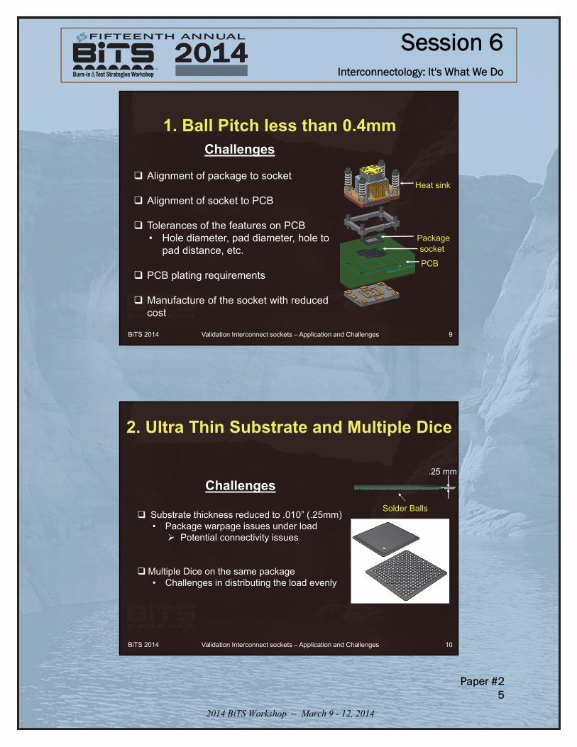
BiTS 2014 Validation Interconnect sockets – Application and Challenges 9
1. Ball Pitch less than 0.4mmChallenges
Alignment of package to socket
Alignment of socket to PCB
Tolerances of the features on PCB• Hole diameter, pad diameter, hole to
pad distance, etc.
PCB plating requirements
Manufacture of the socket with reduced cost
socketPackage
PCB
Heat sink
BiTS 2014 Validation Interconnect sockets – Application and Challenges 10
2. Ultra Thin Substrate and Multiple Dice
Challenges
Substrate thickness reduced to .010” (.25mm)• Package warpage issues under load Potential connectivity issues
Multiple Dice on the same package• Challenges in distributing the load evenly
.25 mm
Solder Balls

2014 BiTS Workshop ~ March 9 - 12, 2014
Paper #26
Interconnectology: It's What We Do
Session 6
BiTS 2014 Validation Interconnect sockets – Application and Challenges 11
3. Multiple Solder Dimensions on the Same Package
Solder ball height variation
Challenges
Mixed Solder Resist Openings (SROs) on the same package
• Ball height along the outer perimeter is taller than the inner one
• Polymer socket contact working range is small (<5mils) – potential reliability issues
BiTS 2014 Validation Interconnect sockets – Application and Challenges 12
4. Sockets for PoP PackagesChallenges
Memory socket on top of SoC socket
Through-Mold-Interconnect (TMI) challenges
Socket contacts that connect to balls on the bottom and top
Pitch scaling down to .35mm for memory packages
Through-Mold-Interconnect
Memory Socket
SoC Socket
MemoryPackage
SoC Package
Motherboard
PoP Package/Socket Schematic
F
F

2014 BiTS Workshop ~ March 9 - 12, 2014
Paper #27
Interconnectology: It's What We Do
Session 6
4. Multi-PoP PackagesChallenges
Multiple sockets on top of the main socket with over 2,000 solder balls
Alignment of memory package sockets on top of the substrate (0.4 mm pitch)
Large force required to make connectivity
Memory SocketSoC Socket
Memory Package
SoC Package
Motherboard
Memory SocketMemory Package
Multiple PoP Package/Socket Schematic
F F
F F
BiTS 2014 Validation Interconnect sockets – Application and Challenges 13
BiTS 2014 Validation Interconnect sockets – Application and Challenges 14
5. Use of Sockets with Zero Keep-outChallenges
Thickness of the board is 0.8mm – subject to warpage and deflection
No alignment and mounting holes in the validation board due to routing constraint
Base Plate
Validation board
ClampSoCSocket
PedestalAlignment pin
Socket Assembly Concept
Standoff
Design Concept:

2014 BiTS Workshop ~ March 9 - 12, 2014
Paper #28
Interconnectology: It's What We Do
Session 6
6. High Temperature Testing
Challenges
Socket reliability at high temperature (>70°C) and thermal cycling (0°C to 100°C)
Polymer properties change with temperature change
The contact resistance becomes unstable at extreme temperatures and during thermal cycling
• Max contact resistance can go up to 250 milliohms (for 0.4mm pitch socket)
• Need to reseat the package into the socket to achieve lower contact resistance
BiTS 2014 Validation Interconnect sockets – Application and Challenges 15
Challenges• More and more devices are soldered down in the final
product -- Need for more validation socket designs
• Number of validation socket designs growing due to increased number of derivative products
• Validation to move to more “real world devices” (Form-Factor-Designs -- FFDs) and away from “artificial boards” (Debug and Validation Platform -- DVP)– Need for more innovative socket designs and hit a price point with
“Zero Keep-out” sockets
BiTS 2014 Validation Interconnect sockets – Application and Challenges 16
7. Validation Socket Scope

2014 BiTS Workshop ~ March 9 - 12, 2014
Paper #29
Interconnectology: It's What We Do
Session 6
Summary Validation sockets play a critical role in reducing
validation time
Validation sockets have significant technology challenges for socketing SoC devices
Need Industry help to meet challenging future validation socket requirements– Low height
– “Zero Keep-out” (X and Y) – Same size as the package
– Low cost
– Low force
– Dense ball pitch up to 0.3mm
– Shorter lead time
BiTS 2014 Validation Interconnect sockets – Application and Challenges 17